Embed Size (px)
Citation preview

Copyright © Cirrus Logi(All Rights Reserwww.cirrus.com
CS5467
+2.5V reference
CS
SDI
SDOSCLK
INT
RESET
REF
+5V GND VD+_EXT
IN OUTVREF
4.096MHz Crystal
VIN2+
VIN2-
IIN2+
IIN2-
IIN1+
IIN1-
VIN1+
VIN1-
E1
E2
E3
MODE
CDB5467U
CDB5467U Engineering Board and GUI Software
FeaturesVoltage and Current Interface
USB Communication with PC
On-board C8051F320 Microcontroller
On-board Voltage Reference
LabWindows®/CVI® GUI Software– Register Setup & Chip Control
– FFT Analysis
– Time Domain Analysis
– Noise Histogram Analysis
"Auto-boot" Demo with Serial EEPROM
General DescriptionThe CDB5467U is an inexpensive tool designed to evaluatethe functionality and performance of the CS5467 analog-to-dig-ital converter (ADC). The evaluation board includes an LT1019voltage reference, a C8051F320 microcontroller with a USB in-terface, and firmware. The microcontroller controls the serialcommunication between the evaluation board and the PC viathe firmware, enabling quick and easy access to all oftheCS5467's registers and functions.
The CDB5467U includes software for data capture, time do-main analysis, histogram analysis, and frequency domainanalysis.
Schematics in PADS™ PowerLogic™ format are available fordownload at www.cirrus.com/IndustrialSoftware.
ORDERING INFORMATIONCDB5467U Evaluation Board
c, Inc. 2007ved) OCT ‘07
DS714DB1
C8051F320
USB
Reset Circuirty
SERIALEERPOM
RESET BUTTON
Vu+_EXT

CDB5467U
TABLE OF CONTENTS1. HARDWARE ............................................................................................................................. 3
1.1 Introduction ........................................................................................................................ 31.2 Evaluation Board Overview ................................................................................................ 31.3 Analog Section ................................................................................................................... 41.4 Digital Section .................................................................................................................... 51.5 Power Supply Section ........................................................................................................ 51.6 Auto-boot Mode ................................................................................................................. 6
2. SOFTWARE .............................................................................................................................. 82.1 Installation .......................................................................................................................... 82.2 Using the Software ............................................................................................................. 82.3 Start-up Window ................................................................................................................ 82.4 Setup Window .................................................................................................................. 122.5 Calibration Windows ........................................................................................................ 142.6 Conversion Window ......................................................................................................... 162.7 Pulse Rate Window .......................................................................................................... 182.8 Data Collection Window ................................................................................................... 192.9 EEPROM Window ............................................................................................................ 262.10 Debug Panel .................................................................................................................. 27
Appendix A. Bill Of Materials ................................................................................................... 28Appendix B. Schematics .......................................................................................................... 30Appendix C. Layer Plots ........................................................................................................... 34
LIST OF FIGURESFigure 1. CDB5463U Assembly Drawing ........................................................................................ 3Figure 2. GUI Start-up Window ....................................................................................................... 8Figure 3. Setup Menu Showing Successful USB Connection ......................................................... 9Figure 4. USB Error Message ......................................................................................................... 9Figure 5. Data from Disc File Selection Window ........................................................................... 10Figure 6. Data from Disc File Selection Window ........................................................................... 11Figure 7. Quit Dialog ..................................................................................................................... 11Figure 8. Setup Window ................................................................................................................ 12Figure 9. Calibration Window ........................................................................................................ 14Figure 10. Conversion Window ..................................................................................................... 16Figure 11. Pulse Rate Output Window .......................................................................................... 18Figure 12. Data Collection Window ............................................................................................... 19Figure 13. Configuration Window .................................................................................................. 20Figure 14. Histogram Analysis ...................................................................................................... 22Figure 15. FFT Analysis ................................................................................................................ 24Figure 16. Time Domain Analysis ................................................................................................. 25Figure 17. EEPROM Window........................................................................................................ 26Figure 18. Debug Panel ................................................................................................................ 27Figure 19. Schematic - Analog Inputs ........................................................................................... 30Figure 20. Schematic - CS5463 & Socket..................................................................................... 31Figure 21. Schematic - Microcontroller & USB Interface............................................................... 32Figure 22. Schematic - Power Supplies ........................................................................................ 33Figure 23. Top Silkscreen ............................................................................................................. 34Figure 24. Top Routing.................................................................................................................. 35Figure 25. Bottom Routing ............................................................................................................ 36Figure 26. Bottom Silkscreen ........................................................................................................ 37
2 DS714DB1

CDB5467U
1. HARDWARE1.1 IntroductionThe CDB5467U evaluation board provides a convenient means of evaluating the CS5467 power mea-surement IC. The CDB5467U evaluation board operates from a single +5V power supply. The evaluationboard interfaces the CS5467 to a PC via a USB cable. To accomplish this, the board comes equippedwith a C8051F320 microcontroller and a USB interface. Additionally, the CDB5467U GUI software pro-vides easy access to the internal registers of the CS5467. The software also provides a means to displaythe performance in the time domain or frequency domain.
1.2 Evaluation Board OverviewThe board is partitioned into two main sections: analog and digital. The analog section consists of theCS5467 and a precision voltage reference. The digital section consists of the C8051F320 microcontroller,EEPROM, the hardware test switches, the reset circuitry, and the USB interface. The board also has auser friendly power supply connection.
Figure 1. CDB5467U Assembly Drawing
4.096 MHz
CDB5467U
54
67
DS714DB1 3

CDB5467U
1.3 Analog SectionThe CDB5467U evaluation board provides screw-type terminals (J21, J23, J27, & J28) to connect inputsignals to the voltage and current channels. The screw terminals are labels as VIN2-, VIN2+, VIN1-,VIN1+, IIN1+, IIN1-, and IIN2+, IIN2-. An R-C network at each channel input provides a simple anti-aliasfilter.
The evaluation board provides three voltage reference options for VREFIN to the CS5467. The three volt-age reference options include: VREFOUT from CS5467, the on-board +2.5V reference, and externalREF+ (screw terminal J14). Table 1 and Table 2 illustrate the options available for VREFIN. With a jumperon J25 in the position labeled VREFOUT, the reference is supplied by the on-chip voltage reference. Witha jumper on J25 in the position labeled VREF, the reference is supplied by an off-chip voltage reference.
Table 2 illustrates the options available for VREF. With a jumper on J12 in position LT1019, the LT1019provides a +2.5V reference (the LT1019 was chosen for its low drift - typically 5 ppm/°C). By setting thejumper on J12 to position REF+, an external voltage reference is supplied via screw terminal J14's REF+input.
The three input signal options for the voltage (VIN1±, VIN2±) and current (IIN1±, IIN2±) channels inputinclude: an external signal (screw terminals J21, J23, J27, and J28), GND, or VREF. Table3 illustrates theoptions available. By installing jumpers on J11 to position VIN2-, J7 to position VIN2+, J17 to positionVIN1-, J22 to position VIN1+, J24 to position IIN1+, J26 to position IIN1-, J20 to position IIN2+, and J19to position IIN2-, the input voltage signal is supplied from the screw terminals J21, J23, J27, and J28. Witha jumper on J11, J7, J17, J22, J24, J26, J20 and J19 in the GND position, the inputs are connected to
Reference Description J25
VREFOUT Selects On-chipReference (25 ppm/°C)
VREF Selects External or LT1019 Reference(J12)
Table 1. Internal Voltage Reference Selection for VREF
Reference Description J12
LT1019Selects On-board LT1019 Reference
(5 ppm/°C)
REF+Selects External
Reference Source (J14)
Table 2. External Voltage Reference Selection for VREF
O O
VREF VREFIN VREFOUT (Default)
O O
VREF VREFIN VREFOUT
O VREFO O VREF
LT1019 REF+
O VREFO O VREF
LT1019 REF+
(Default)
4 DS714DB1

CDB5467U
analog ground (AGND). With a jumper on J11, J7, J17, J22, J24, J26, J20 and J19 in position VREF, theinputs are connected to the reference voltage selected on J12.
1.4 Digital SectionThe digital section contains the microcontroller, USB interface, JTAG header, reset circuitry, and an ex-ternal interface header (J40). The microcontroller interfaces the SPI of CS5467 with the USB connectionto the PC, enabling the GUI software to access all the CS5467 registers and functions. Interface header,J40, is provided to allow the CDB5467U to be connected to an external energy registration device or anexternal microcontroller. To connect the CS5467 to an external microcontroller, R57, R58, R59, R60, R61,and R62 must be removed from the board. The energy output pins E1, E2, and E3 are routed to LEDswhich provide a simple visual check of the energy output pulses. The MODE pin is also routed to a LEDto indicate whether the CS5467 is operating in auto-boot mode. Jumpers J10, J13, J15, and J16 areequipped at the factory with jumpers to enable the LEDs.
INPUT Description J11 J7 J17 J22
VIN2± or VIN1± Selects ExternalSignal
VIN2± or VIN1± Selects ExternalSignal
GND Selects Grounding the Input
VREFIN Selects Reference Source
INPUT Description J24 J26 J20 J19
IIN1± or IIN2± Selects ExternalSignal
IIN1± or IIN2± Selects ExternalSignal
GND Selects Grounding the Input
VREFIN Selects Reference Source
Table 3. Voltage and Current Channel Input Signal Selection
O VIN2-O O VIN2-O O VIN2-
GND VREF VIN2- (Default)
O VIN2+O O VIN2+O O VIN2+
VIN2+ VREF GND (Default)
O VIN1-O O VIN1-O O VIN1-
GND VREF VIN1- (Default)
O VIN1+O O VIN1+O O VIN1+
VIN1+ VREF GND (Default)
O VIN2-O O VIN2-O O VIN2-
GND VREF VIN2-
O VIN2+O O VIN2+O O VIN2+
VIN2+ VREF GND
O VIN1-O O VIN1-O O VIN1-
GND VREF VIN1-
O VIN1+O O VIN1+O O VIN1+
VIN1+ VREF GND
O VIN2-O O VIN2-O O VIN2-
GND VREF VIN2-
O VIN2+O O VIN2+O O VIN2+
VIN2+ VREF GND
O VIN1-O O VIN1-O O VIN1-
GND VREF VIN1-
O VIN1+O O VIN1+O O VIN1+
VIN1+ VREF GND
O VIN2-O O VIN2-O O VIN2-
GND VREF VIN2-
O VIN2+O O VIN2+O O VIN2+
VIN2+ VREF GND
O VIN1-O O VIN1-O O VIN1-
GND VREF VIN1-
O VIN1+O O VIN1+O O VIN1+
VIN1+ VREF GND
O IIN1+O O IIN1+-O O IIN1+
GND VREF IIN1+ (Default)
O IIN1-O O IIN1-O O IIN1-
IIN1- VREF GND (Default)
O IIN2+O O IIN2+O O IIN2+
GND VREF IIN2+ (Default)
O IIN2-O O IIN2-O O IIN2-
IIN2- VREF GND (Default)
O IIN1+O O IIN1+-O O IIN1+
GND VREF IIN1+
O IIN1-O O IIN1-O O IIN1-
IIN1- VREF GND
O IIN2+O O IIN2+O O IIN2+
GND VREF IIN2+
O IIN2-O O IIN2-O O IIN2-
IIN2- VREF GND
O IIN1+O O IIN1+-O O IIN1+
GND VREF IIN1+
O IIN1-O O IIN1-O O IIN1-
IIN1- VREF GND
O IIN2+O O IIN2+O O IIN2+
GND VREF IIN2+
O IIN2-O O IIN2-O O IIN2-
IIN2- VREF GND
O IIN1+O O IIN1+-O O IIN1+
GND VREF IIN1+
O IIN1-O O IIN1-O O IIN1-
IIN1- VREF GND
O IIN2+O O IIN2+O O IIN2+
GND VREF IIN2+
O IIN2-O O IIN2-O O IIN2-
IIN2- VREF GND
DS714DB1 5

CDB5467U
1.5 Power Supply SectionTable 4 illustrates the power supply connections to the evaluation board. The +5V binding post (J3) sup-plies the positive analog (VA+) for the CS5467 and the +2.5V reference. The VD+_EXT binding post (J5)supplies the digital section of the CS5467 (VD+) and level shifters. Jumper J8 allows the VD+ supply tobe sourced from the VD+_EXT binding post (J5), the +5V binding post (J3), or the regulated 3.3V supplyderived from the microcontroller. The Vu+_EXT (J6) binding post supplies the positive supply for the 8051microcontroller (8051_REGIN). Jumper J9 allows the 8051_REGIN supply to be sourced from either theVu+_EXT binding post (J6), +5V binding post (J3) or VD+_EXT binding post (J5).
Power Supplies Power Post Connections VD+ 8051-REGINAnalog (VA+) Digital (VD+) 8051 (Vu+) +5V GND VD+EXT VU+EXT J8 J9
+5 +5 +5 +5 0
NC
NC
+5
NC
+5
NC
+5
NC
+5 +3.3 +5 +5 0
NC
NC
+5
+3.3
NC
+5
Table 4. Power Supply Connections
O VD+O O VD+O O VD+
VD+_EXT +5 +3.3 (Default)
O 8051O O 8051O O 8051
Vu+_EXT +5 VD+ (Default)
O VD+O O VD+O O VD+
VD+_EXT +5 +3.3
O 8051O O 8051O O 8051
Vu+_EXT +5 VD+
O VD+O O VD+O O VD+
VD+_EXT +5 +3.3
O 8051O O 8051O O 8051
Vu+_EXT +5 VD+
O VD+O O VD+O O VD+
VD+_EXT +5 +3.3
O 8051O O 8051O O 8051
Vu+_EXT +5 VD+
O VD+O O VD+O O VD+
VD+_EXT +5 +3.3
O 8051O O 8051O O 8051
Vu+_EXT +5 VD+
O VD+O O VD+O O VD+
VD+_EXT +5 +3.3
O 8051O O 8051O O 8051
Vu+_EXT +5 VD+
O VD+O O VD+O O VD+
VD+_EXT +5 +3.3
O 8051O O 8051O O 8051
Vu+_EXT +5 VD+
O VD+O O VD+O O VD+
VD+_EXT +5 +3.3
O 8051O O 8051O O 8051
Vu+_EXT +5 VD+
O VD+O O VD+O O VD+
VD+_EXT +5 +3.3
O 8051O O 8051O O 8051
Vu+_EXT +5 VD+
O VD+O O VD+O O VD+
VD+_EXT +5 +3.3
O 8051O O 8051O O 8051
Vu+_EXT +5 VD+
6 DS714DB1

CDB5467U
1.6 Auto-boot ModeWith a jumper connection on J18 (AUTO-BOOT ENABLE), the CS5467 operates in auto-boot mode andthe CDB5467U board operates as a stand-alone system without attaching it up to a PC. When in auto-boot mode, a hardware reset (press on S1) will cause the CS5467 to boot up using the serial data fromthe serial EEPROM on the board (U10). When the CS5467 is in auto-boot mode, the SPI connectionsbetween the microcontroller and the CS5467 are removed and the GUI software can not access theCS5467 registers and functions.
The EEPROM must be programmed prior to the auto-boot sequence. When the CDB5467U EvaluationBoard is sent from the factory, the EEPROM is programmed with the following CS5467 command/datasequence:
1. Move to EEPROM page 1:
0x7E 0x00 0x00 0x012. Write Modes register, turn high-pass filters on:
0x60 0x00 0x01 0xE03. Move to EEPROM page 0:
0x7E 0x00 0x00 0x004. Set bit 2 (LSD) in the Mask register:
0x74 0x00 0x00 0x045. Start continuous conversion:
0xE86. Write STOP bit in Control register, to terminate auto-boot sequence:
0x78 0x00 0x01 0x00
This sequence programs the CS5467 for continuous conversion mode. If voltage and current signals areapplied to the inputs, the CS5467 will issue pulses on the E1 pin. See the CS5467 data sheet for moredetails on auto-boot.
DS714DB1 7

CDB5467U
2. SOFTWAREThe evaluation board comes with software and an USB cable to link the evaluation board to the PC. Theevaluation software was developed with LabWindows®/CVI®, a software development package from na-tional Instruments. The evaluation software is available for download on the Cirrus Logic web site at http://www.cirrus.com/industrialsoftware and was designed to run under Windows® 2000 orWindows XP®.
2.1 InstallationTo install the software, go to the Cirrus Logic web site at http://www.cirrus.com/industrialsoftware and re-fer to application note AN278.
2.2 Using the SoftwareBefore launching the software, check all jumper settings on the CDB5467U evaluation board as describedin Section 1, and connect the board to an open USB port on the PC using the provided cable. Once theboard is powered on, the software program can be launched.
2.3 Start-up WindowWhen the software is launched, the start-up window will appear. This window contains information con-cerning the software's title, revision number, copyright date, etc. See Figure 2.
Figure 2. GUI Start-up Window
At the top of the screen is a menu bar which displays user options. The menu bar has three items: Menu,Setup, and Quit. Initially Menu is disabled. After establishing a link to a data source, the Menu item willbecome available.
8 DS714DB1

CDB5467U
2.3.1 Setup MenuSetup allows user to establish a USB communication connection with CDB5467U board or select a pre-viously saved data file for further analysis.
If the USB item in the Setup menu is selected, the evaluation software will poll the CDB5467U, verifyingthe serial communication link is ready. At this point, the USB menu item is checked indicating that the PChas successfully communicated with CDB5467U evaluation board, and device and micro-code versioninformation are read from the board and displayed on the screen. See Figure 3. Due to improvements tothe software or new features being added, the version displayed may be different than the image shownhere.
Figure 3. Setup Menu Showing Successful USB Connection
If the evaluation software is unable to establish a communication link with the CDB5467U board, a mes-sage will appear, indicating that the initial communication has failed. See Figure 4.
Figure 4. USB Error Message
Check to verify that the USB cable is connected properly and the power supply is on and connected prop-erly to the CDB5467U. Reset the board (press the RESET button on the board) and try to setup the USBconnection again.
DS714DB1 9

CDB5467U
If the Data from Disk item in the Setup menu is selected, a file selection window will appear as shown inFigure 5. User can select a pre-saved data file for further analysis using time domain, FFT, and histogramplots in Data Collection Window of the software.
Figure 5. Data from Disc File Selection Window
2.3.2 Menu MenuExcluding the Start-Up window, the Menu menu provides 7 options: Setup Window, Calibration Window,Conversion Window, Pulse Rate Window, Data Collection Window, EEPROM Window, and Debug Win-dow. Each window provides a means to evaluate the different functions and performance of the CS5467.Each option has an associated function key (<F1>, <F2>, etc.). See Figure 6.
Figure 6. Menu Pull-down Options
10 DS714DB1
CDB5467U
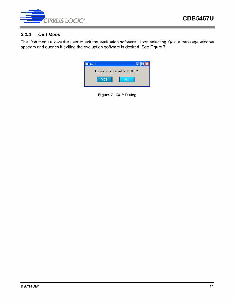
2.3.3 Quit MenuThe Quit menu allows the user to exit the evaluation software. Upon selecting Quit, a message windowappears and queries if exiting the evaluation software is desired. See Figure 7.
Figure 7. Quit Dialog
DS714DB1 11

CDB5467U
2.4 Setup WindowThe evaluation software provides access to the CS5467's internal registers through the Setup window.See Figure 8. The user can enter the Setup window by pulling down the Menu menu and selecting SetupWindow, or by pressing <F2> on the keyboard.
In the Setup window, all of the CS5467's registers are displayed in hexadecimal notation and are decodedto provide easier readability. Refer to the CS5467 data sheet for information on register functionality anddefinitions. See Figure 8.
Figure 8. Setup Window
12 DS714DB1

CDB5467U
2.4.1 Refresh Screen ButtonThe Refresh Screen button will update the contents of the screen by reading all the register values fromthe CS5467. It is a good idea to press the Refresh Screen button when entering the Setup window, orafter modifying any registers, to reflect the current status of the CS5467.
2.4.2 Reset DUT ButtonThe Reset DUT button will hardware reset the CS5467. The CS5467 will perform a reset as discussed inthe CS5467 data sheet. After the hardware reset to the CS5467 device, the screen contents will be auto-matically refreshed with the updated status of the CS5467.
2.4.3 CS5467 Crystal FrequencyThe CS5467 accepts a wide range of crystal input frequencies, and can therefore run at many differentsample rates. The crystal frequency being used on the CS5467 should be entered in this box to provideaccurate frequency calculation in the FFT window. This will also help the software decide which functionsthe evaluation system can perform reliably.
2.4.4 Configuration RegisterIn the Configuration Register box, the contents of the Config register can be modified by typing a hexa-decimal value in the HEX: field, or by changing any of the values below the HEX: field to the desired set-tings. Although the CDB5467U software allows the user to modify any of the bits in the Config register,changing certain bits may cause the software and board to behave erratically. For the evaluation systemto function properly, the IMODE, IINV field should be set to the default Active Low. This applies only tothe CDB5467U evaluation system, and not to the CS5467 chip itself.
2.4.5 Control RegisterThe Control Register section is used to make changes to and display the contents of the Ctrl register. TheCtrl register contains various bits used to activate or terminate various features of the CS5467. Refer tothe CS5467 data sheet for descriptions of the bits. The user is able to turn each bit on or off individually.The value of the Ctrl register is displayed in Hexadecimal format. Most of the Ctrl register bits are reservedor unused. Only the usable bits are displayed in the Setup Window.
2.4.6 Mask Register / Status RegisterThe Mask Register / Status Register box displays the values for these registers in hexadecimal and de-codes them to indicate each bit's function. The Mask register can be modified by typing a value in theHEX: field, or by checking the appropriate check boxes for the bits that are to be masked. The Status reg-ister cannot be directly modified. It can only be reset by pressing the Clear Status Register button. TheHEX: field for this register and the lamps are indicators only. A lamp which is on means that the corre-sponding bit in the Status register is set (except the Invalid Command bit, which is inverted). The valuepresent in the Mask register may be changed by the software during certain operations to provide correctfunctionality of the CDB5467U board.
2.4.7 Temperature, Voltage SAG, Current Fault RegistersThese boxes display the values of the corresponding registers in both hexadecimal and decimal format.Each register can be modified by typing a value in the corresponding offset, level, duration, or gain valuefield (decimal) or HEX: field (hexadecimal).
DS714DB1 13

CDB5467U
2.4.8 Cycle Count / Pulse Output RegistersThese fields display the values of corresponding register in both hexadecimal and decimal format. Eachregister can be modified by typing a value in the corresponding Decimal Value or HEX: field.
2.4.9 Voltage Sag / Current Fault / Ichanlevel / Emin (Irmsmin) / VFrms / Tsettle / LoadMIN / Epsilon / Temperature Rigisters
These boxes display the values of the corresponding register in both hexadecimal and decimal format.Each register can be modified by typing a value in the corresponding Decimal Value or HEX: field.
2.5 Calibration WindowsThe Calibration window is used to display and write to the CS5467 offset and gain calibration registers.The user is also able to initiate the CS5467's calibration sequences that are used to set the calibrationvalues. Both AC and DC calibrations can be run for offset and gain, for either the voltage channel or thecurrent channel, or both simultaneously. The user should refer to the CS5467 data sheet for more detailson calibration.
The Refresh Screen button will update the contents of the screen by reading all the register values fromthe part. It is a good idea to press the Refresh Screen button when entering the Calibration window, orafter modifying any registers to reflect the current status of the CS5467.
Figure 9. Calibration Window
14 DS714DB1

CDB5467U
2.5.1 Offset / Gain RegisterIn the offset and gain register boxes, the offset and gain registers for all channels are displayed in hexa-decimal and decimal. These registers can be modified directly by typing the desired value in the hexadec-imal display boxes. There are three types of offset registers: DC offset, AC offset and power offset. TheAC offset registers only affect the RMS register values. The power offset registers only affect the activepower register values. The DC/AC/power offset register is a two's complement number whose value rang-es from -1 to +1. The gain register value ranges from 0 to 4.
2.5.2 Performing CalibrationsAC/DC offset and gain calibrations can be performed on both the voltage and current channels of theCS5467. It is generally a good idea to software-reset the CS5467 before running calibrations, becausethe initial values in the calibration registers will affect the results of the calibration. A software reset willreset these registers back to the default values of zero offset and unity gain. AC/DC offset calibrationshould be performed before gain calibration to ensure accurate results.
2.5.2.1 Offset Calibrations1. Ground the channel(s) you want to calibrate directly at the channel header(s), J11 and J7 for voltage chan-
nel 2, J17 and J22 for voltage channel 1, J24 and J26 for current channel 1, and J20 and J19 for currentchannel 2. The channel(s) could also be grounded directly at the screw-type terminals.
2. Press the corresponding AC or DC offset calibrate button (Cal V, Cal I, or Calibrate All Channels) beside orbelow the offset register boxes.
3. The offset register value(s) will automatically update when the calibration is completed.
2.5.2.2 Gain Calibrations1. Attach an AC or DC calibration signal to the screw-type terminals, and make sure the corresponding chan-
nel headers (J11, J7, J17, J22, J24, J26, J20 and J19) are set to the input position.
2. Press the corresponding AC or DC gain calibrate button (Cal V, Cal I, or Calibrate All Channels) beside orbelow the gain register boxes.
3. The gain register value(s) will automatically update when the calibration is completed.
The Calibration window also contains the Power Offset Register1 / 2 display and adjustment. The usercan read and write the values in the power offset registers (P1off / P2off).
DS714DB1 15

CDB5467U
2.6 Conversion WindowThe Conversion Window allows the user to see the results of single and continuous conversions, performdata averaging, and utilize the power-saving modes of the CS5467. See Figure 10. The Conversion Win-dow can be accessed from the Menu pull-down and selecting Conversion Window, or by pressing <F4>.
Figure 10. Conversion Window
2.6.1 Single Conversion ButtonPressing this button will cause a single conversion to be performed. After a single conversion is complete,the Result column will be updated with the values present in each data register.
2.6.2 Continuous Conversion ButtonPressing this button will cause continuous conversions to be performed until the user presses the Stopbutton. After each conversion is complete, the Result column will be updated with the values present ineach data register. The Mean and Standard Deviation columns will be updated every N cycles, where Nis the number in the Samples to Average field. If the Samples to Average is set to a large number, it maytake many collection cycles after pressing the Stop button before the data actually stops being collected.
16 DS714DB1

CDB5467U
2.6.3 Standby / Sleep Mode ButtonsWhen these buttons are pressed, the CS5467 will enter either standby or sleep power saving modes. Toreturn to normal mode, press the Power Up button.
2.6.4 Power Up ButtonThis button is used to send the Power Up/Halt command to the CS5467. The part will return to normaloperating mode and halt any conversions that are being done at this time.
2.6.5 Set Line FrequencyIf the AFC bit in the Mode register is set, the Epsilon register will be calculated automatically by theCS5467 and the Line Frequency display field will be updated automatically in continuous conversionmode. If the AFC bit in the Mode register is not set and the line frequency is other than the default value(50Hz), to ensure the accuracy of the quadrature power (Q1, Q2) and the reactive power (Q1avg, andQ2avg), the line frequency must be set manually here to make Epsilon be the ratio of line frequency tothe output word rate (OWR). Refer to the CS5467 datasheet for more details.
2.6.6 Temperature Settings WindowThe Temperature Settings Window is used to adjust the temperature offset register (Toffset) and temper-ature gain register (Tgain) to convert the temperature register (T) from a Celsius scale (°C) to a Fahrenheitscale (°F) or vice versa and to improve temperature measurement accuracy. Refer to the CS5467 datasheet for the details of the on-chip temperature sensor.
2.6.7 Write Data to File WindowThis window provides a means to write the conversion result data to a .txt text file for later analysis orprint out. The file path and name will be shown in Filename field. The Open File button is used to open anew or existing .txt text file for data writing. Each time the Write Data button is pressed, the result data iswritten into the file and the Number of Lines Written field value will be increased by 1.
2.6.8 Temperature MeasurementIn the CS5467, voltage 2 and temperature are multiplexed on one ADC channel. To initiate a temperaturemeasurement, write 1 to the Tmeas register while in continuous conversion mode. When the Tmeas reg-ister returns to 0, the Temperature field should be updated with the data in the T (Temperature) register.
DS714DB1 17
CDB5467U
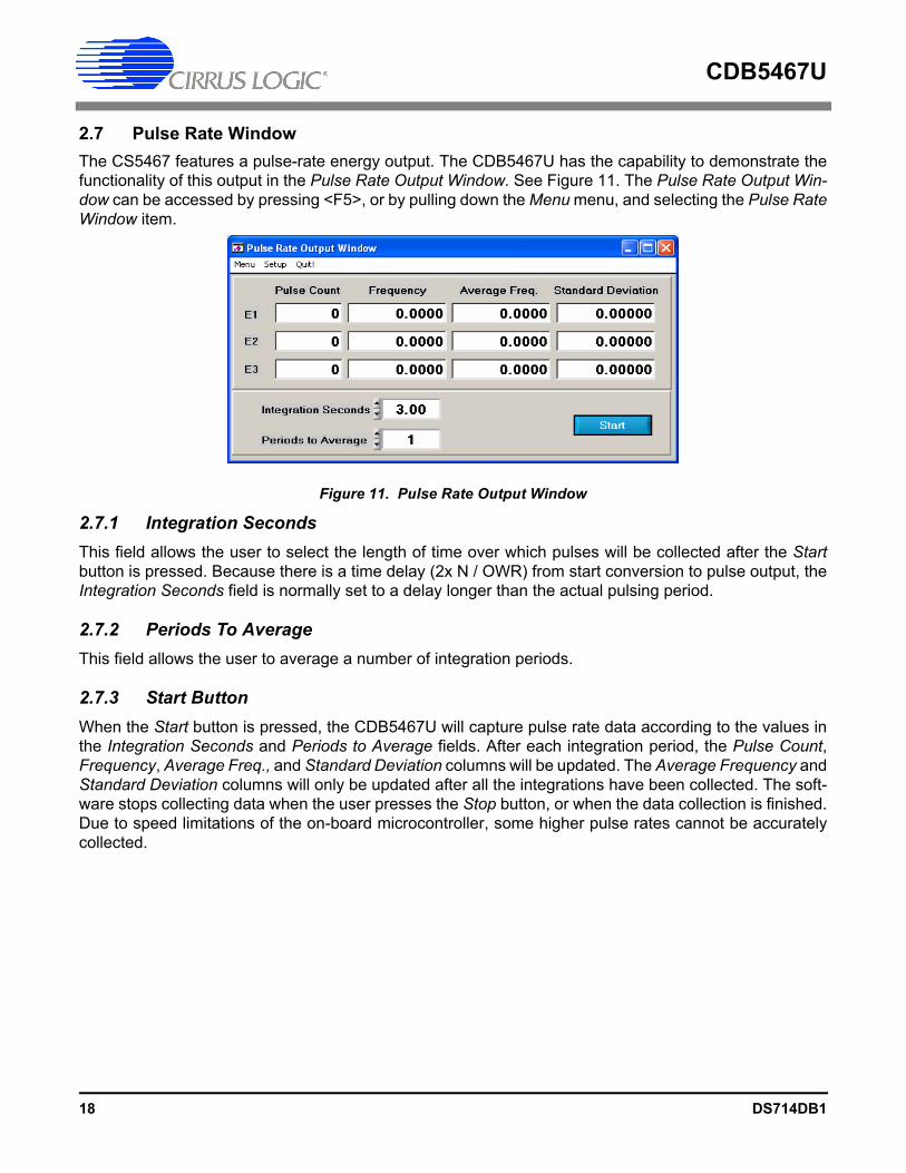
2.7 Pulse Rate WindowThe CS5467 features a pulse-rate energy output. The CDB5467U has the capability to demonstrate thefunctionality of this output in the Pulse Rate Output Window. See Figure 11. The Pulse Rate Output Win-dow can be accessed by pressing <F5>, or by pulling down the Menu menu, and selecting the Pulse RateWindow item.
Figure 11. Pulse Rate Output Window
2.7.1 Integration SecondsThis field allows the user to select the length of time over which pulses will be collected after the Startbutton is pressed. Because there is a time delay (2x N / OWR) from start conversion to pulse output, theIntegration Seconds field is normally set to a delay longer than the actual pulsing period.
2.7.2 Periods To AverageThis field allows the user to average a number of integration periods.
2.7.3 Start ButtonWhen the Start button is pressed, the CDB5467U will capture pulse rate data according to the values inthe Integration Seconds and Periods to Average fields. After each integration period, the Pulse Count,Frequency, Average Freq., and Standard Deviation columns will be updated. The Average Frequency andStandard Deviation columns will only be updated after all the integrations have been collected. The soft-ware stops collecting data when the user presses the Stop button, or when the data collection is finished.Due to speed limitations of the on-board microcontroller, some higher pulse rates cannot be accuratelycollected.
18 DS714DB1

CDB5467U
2.8 Data Collection WindowThe Data Collection Window (Figure 12) allows the user to collect sample sets of data from the CS5467and analyze them using time domain, FFT, and histogram plots. The Data collection Window can be ac-cessed by pulling down the Menu menu, and selecting the Data Collection Window item, or by pressing<F6>.
Figure 12. Data Collection Window
2.8.1 Time Domain / FFT/ Histogram SelectorThis menu selects the type of data processing to perform on the collected data and display in the plot area.Refer to the Analyzing Data section for more information.
2.8.2 Config ButtonThis button will bring up the Configuration window, in which the user can modify the data collection spec-ifications. Refer to the Configuration Window section in this document for more information.
2.8.3 Collect ButtonThis button will collect data from the part, to be analyzed in the plot area. See the Collecting Data Setssection for more information.
DS714DB1 19

CDB5467U
2.8.4 Output ButtonThis button will bring up a window in which the user can output the data to a file for later use, print out aplot, or print out the entire screen. When saving data, only the data channel being displayed on the plotwill be saved to a file.
2.8.5 Zoom ButtonThis button allows the user to zoom in on the plot by selecting two points in the plot area. Press the Re-store button to return to the normal data plot, or press the Zoom button again to zoom in even further.
2.8.6 Channel Select ButtonAfter data collection, the two buttons labeled as “No Data” will be replaced with Current and Voltage but-tons, allowing the user to choose the appropriate channel for display. In the time domain mode, an addi-tional Overlay button will be present which allows the user to display all the channels on the same plot.
2.8.7 Configuration WindowThe Configuration window allows the user to set up the data collection and analysis parameters.
Figure 13. Configuration Window
2.8.7.1 Number of Samples
This field allows the user to select the number of samples to collect, between 16 and 32768.
2.8.7.2 Average
When performing FFT analyses, this field determines the number of FFTs to average. FFTs will be col-lected and averaged when the Collect button is pressed.
20 DS714DB1

CDB5467U
2.8.7.3 FFT Window
This box allows the user to select the type of windowing algorithm for FFT processing. Windowing algo-rithms include the Blackman, Blackman-Harris, Hanning, 5-term Hodie, and 7-term Hodie. The 5-termHodie and 7-term Hodie are windowing algorithms developed at Crystal Semiconductor.
2.8.7.4 Histogram Bin Width
This field determines the "bin width" when plotting histograms of the collected data. Each vertical bar inthe histogram plot will contain the number of output codes entered in this field. Increasing this numbermay allow the user to view histograms with larger input ranges.
2.8.7.5 Data to Collect
These two check boxes allow the user to select the data types that will be collected and returned to thePC for processing.
2.8.7.6 Cycle Count
The value in the Cycle Count field will be written to the Cycle Count register in the CS5467. The CycleCount register determines the length of one computation cycle. The Cycle Count value should be selectedappropriately according to the Data to Collect setting. For example, if the Data to Collect is instantaneouscurrent, voltage, or power it is better to set Cycle Count to 1.
2.8.7.7 Accept Button
When this button is pressed, the current settings will be saved, and the user will return to the Data Col-lection Window.
2.8.8 Collecting Data SetsTo collect a sample data set:
1. In the Data Collection Window, press the Config button to bring up the Configuration window and view thecurrent settings.
2. Select the appropriate settings from the available options (see the Configuration Window section) and pressthe Accept button.
3. The Data Collection Window should still be visible. Press the Collect button to begin collecting data.
4. Once the data has been collected, it can be analyzed, printed, or saved to disk.
2.8.9 Retrieving Saved Data From a FileThe CDB5467U software allows the user to save data to a file, and retrieve it later when needed. To loada previously saved file:
1. Pull down the Setup menu and select the Disk menu item. A file menu will appear.
2. Find the data file in the list and select it. Press the Select button to return.
3. Go to the Data Collection Window, and press the Collect button.
4. The data from the file should appear on the screen. The data will be ready for different types of analysis.
5. To select a different file, repeat the procedure.
DS714DB1 21
CDB5467U
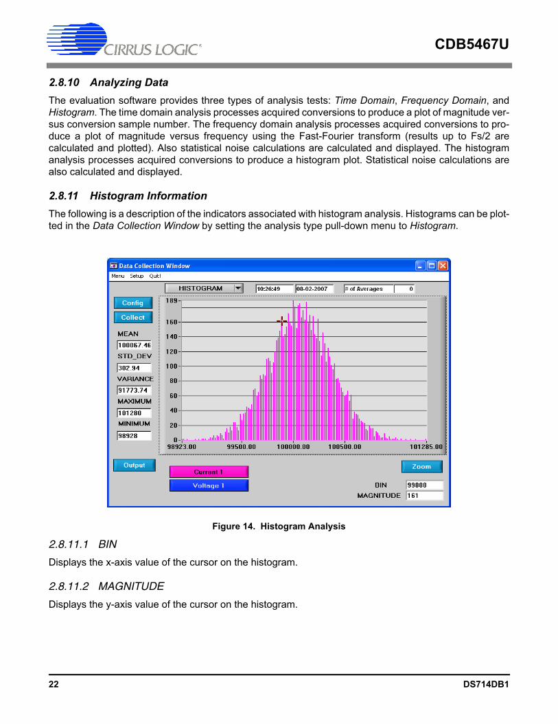
2.8.10 Analyzing DataThe evaluation software provides three types of analysis tests: Time Domain, Frequency Domain, andHistogram. The time domain analysis processes acquired conversions to produce a plot of magnitude ver-sus conversion sample number. The frequency domain analysis processes acquired conversions to pro-duce a plot of magnitude versus frequency using the Fast-Fourier transform (results up to Fs/2 arecalculated and plotted). Also statistical noise calculations are calculated and displayed. The histogramanalysis processes acquired conversions to produce a histogram plot. Statistical noise calculations arealso calculated and displayed.
2.8.11 Histogram InformationThe following is a description of the indicators associated with histogram analysis. Histograms can be plot-ted in the Data Collection Window by setting the analysis type pull-down menu to Histogram.
Figure 14. Histogram Analysis
2.8.11.1 BIN
Displays the x-axis value of the cursor on the histogram.
2.8.11.2 MAGNITUDE
Displays the y-axis value of the cursor on the histogram.
22 DS714DB1

CDB5467U
2.8.11.3 MEAN
Indicates the mean of the data sample set. The mean is calculated using the following formula:
2.8.11.4 STD_DEV
Indicates the standard deviation of the collected data set. The standard deviation is calculated using thefollowing formula:
2.8.11.5 VARIANCE
Indicates for the variance of the current data set. The variance is calculated using the following formula:
2.8.11.6 MAXIMUM
Indicates the maximum value of the collected data set.
2.8.11.7 MINIMUM
Indicates the minimum value of the collected data set.
MeanXi
i 0=
n 1–
∑n
----------------=
STDDEV
Xi MEAN–( )2
i 0=
n 1–
∑n
------------------------------------------------=
VARIANCE
Xi MEAN–( )2
i 0=
n 1–
∑n
------------------------------------------------=
DS714DB1 23

CDB5467U
2.8.12 Frequency Domain InformationThe following describe the indicators associated with FFT (Fast Fourier Transform) analysis. FFT datacan be plotted in the Data Collection Window by setting the analysis type selector to FFT (Figure 15).
Figure 15. FFT Analysis
2.8.12.1 FREQUENCY
Displays the x-axis value of the cursor on the FFT display.
2.8.12.2 MAGNITUDE
Displays the y-axis value of the cursor on the FFT display.
2.8.12.3 S/PN
Indicates the signal-to-peak noise ratio (decibels).
2.8.12.4 SINAD
Indicates for the signal-plus-noise-plus-distortion to noise-plus-distortion ratio (decibels).
2.8.12.5 S/D
Indicates for the signal-to-distortion ratio, 4 harmonics are used in the calculations (decibels).
24 DS714DB1

CDB5467U
2.8.12.6 SNR
Indicates for the signal-to-noise ratio, first 4 harmonics are not included (decibels).
2.8.12.7 FS-Pdb
Indicates for the full-scale to signal Ratio (decibels).
2.8.12.8 Time Domain Information
The following controls and indicators are associated with time domain analysis. Time domain data can beplotted in the Data Collection Window by setting the analysis type selector to Time Domain (Figure 16).
Figure 16. Time Domain Analysis
2.8.12.9 COUNT
Displays current x-position of the cursor on the time domain display.
2.8.12.10 MAGNITUDE
Displays current y-position of the cursor on the time domain display.
2.8.12.11 MAXIMUM
Indicates for the maximum value of the collected data set.
DS714DB1 25
CDB5467U
2.8.12.12 MINIMUM
Indicates for the minimum value of the collected data set.
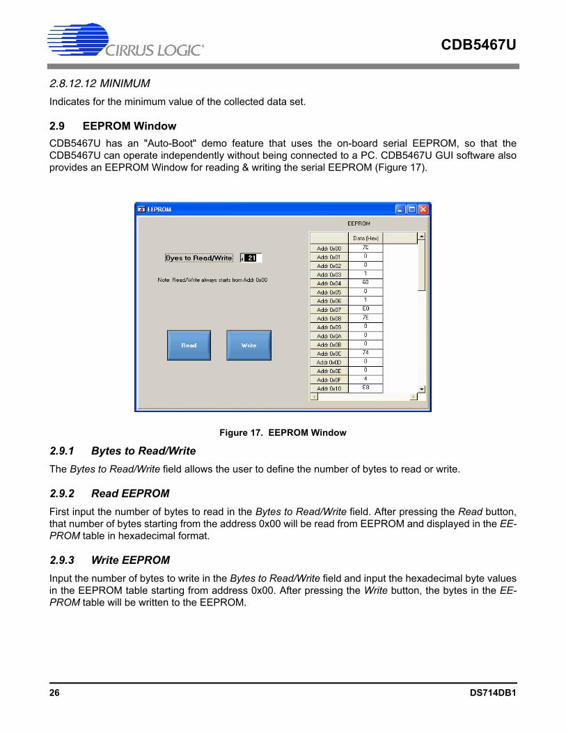
2.9 EEPROM WindowCDB5467U has an "Auto-Boot" demo feature that uses the on-board serial EEPROM, so that theCDB5467U can operate independently without being connected to a PC. CDB5467U GUI software alsoprovides an EEPROM Window for reading & writing the serial EEPROM (Figure 17).
Figure 17. EEPROM Window
2.9.1 Bytes to Read/WriteThe Bytes to Read/Write field allows the user to define the number of bytes to read or write.
2.9.2 Read EEPROMFirst input the number of bytes to read in the Bytes to Read/Write field. After pressing the Read button,that number of bytes starting from the address 0x00 will be read from EEPROM and displayed in the EE-PROM table in hexadecimal format.
2.9.3 Write EEPROMInput the number of bytes to write in the Bytes to Read/Write field and input the hexadecimal byte valuesin the EEPROM table starting from address 0x00. After pressing the Write button, the bytes in the EE-PROM table will be written to the EEPROM.
26 DS714DB1

CDB5467U
2.10 Debug PanelThe Debug panel provides the user a way to access CS5467 registers and send commands to CS5467directly (Figure 18). Refer to 5.15 in CS5467 data sheet for more details.
Figure 18. Debug Panel
DS714DB1 27

CDB5467U
APPENDIX A. BILL OF MATERIALS
CIR
RU
S LO
GIC
CD
B54
67U
-Z N
Pb R
ev_A
.bom
BIL
L O
F M
ATE
RIA
L (P
age
1 of
2)
Des
crip
tion
Qty
Ref
eren
ce D
esig
nato
rM
FGM
FG P
/NN
otes
CA
P 0
.1uF
±10
% 5
0V N
Pb
X7R
120
66
C1
C18
C19
C21
C29
C30
KE
ME
TC
1206
C10
4K5R
AC
CA
P 2
2pF
±5%
50V
C0G
NP
b 08
051
C2
KE
ME
TC
0805
C22
0J5G
AC
CA
P 0
.1uF
±10
% 1
6V X
7R N
Pb
0603
5C
3 C
4 C
26 C
32 C
33K
EM
ET
C06
03C
104K
4RA
CC
AP
47u
F ±2
0% 1
0V E
LEC
NP
b C
AS
E C
2C
5 C
8P
AN
AS
ON
ICE
EE
1AA
470W
RC
AP
0.1
uF ±
5% 5
0V X
7R N
Pb
0805
7C
6 C
7 C
10 C
11 C
12 C
15 C
25K
EM
ET
C08
05C
104J
5RA
CC
AP
220
pF ±
10%
50V
X7R
NP
b 08
058
C9
C17
C20
C24
C27
C34
C35
C36
KE
ME
TC
0805
C22
1K5R
AC
CA
P 0
.018
uF ±
10%
50V
X7R
NP
b 12
064
C13
C23
C37
C38
KE
ME
TC
1206
C18
3K5R
AC
CA
P 1
0uF
±20%
16V
ELE
C N
Pb
CA
SE
A3
C14
C22
C39
PA
NA
SO
NIC
EE
E1C
S10
0SR
CA
P 1
uF ±
10%
25V
X7R
NP
b 12
061
C16
KE
ME
TC
1206
C10
5K3R
AC
CA
P 4
7uF
±20%
16V
NP
b E
LEC
CA
SE
C2
C28
C31
PA
NA
SO
NIC
EE
E1C
A47
0WR
DIO
DE
AR
RA
Y 5
V (T
VS
) ES
D N
Pb
SO
T143
1D
1LI
TTE
LFU
SE
SP
0503
BA
HTG
LED
SU
P R
ED
1.7
V 1
mA
1.6
MC
D N
Pb
SM
D6
D2
D3
D4
D5
D6
D7
CH
ICA
GO
MIN
IATU
RE
CM
D28
-21S
RC
/TR
8/T1
HD
R 5
x2 M
L .1
"CTR
S G
LD N
Pb
1J1
SA
MTE
CTS
W-1
05-0
7-G
-DC
ON
RA
US
B B
LK N
Pb
TH1
J2A
MP
2923
04-1
CO
N B
PO
ST
2" S
ILV
NY
LON
INS
RE
D N
Pb
3J3
J5
J6JO
HN
SO
N
CO
MP
ON
EN
TS11
1-01
02-0
01R
EQ
UIR
ES
WIR
E, 1
.5L
X 0
.25T
X
0.25
T TY
PE
E 2
4/19
BLU
SQ
UIR
ES
E
LEC
. IN
C.
CO
N B
PO
ST
2" S
ILV
NY
LON
INS
BLK
NP
b1
J4JO
HN
SO
N
CO
MP
ON
EN
TS11
1-01
03-0
01R
EQ
UIR
ES
WIR
E, 1
.5L
X 0
.25T
X
0.25
T TY
PE
E 2
4/19
BLU
SQ
UIR
ES
E
LEC
. IN
C.
HD
R 3
x2 M
L .1
"CTR
062
S G
LD N
Pb
10J7
J8
J9 J
11 J
17 J
19 J
20 J
22 J
24 J
26S
AM
TEC
TSW
-103
-07-
G-D
HD
R 2
x1 M
L .1
" 062
BD
ST
GLD
NP
b TH
5J1
0 J1
3 J1
5 J1
6 J1
8S
AM
TEC
TSW
-102
-07-
G-S
HD
R 2
x2 M
L .1
"CTR
.062
BD
S G
LD N
Pb
1J1
2S
AM
TEC
TSW
-102
-07-
G-D
CO
N T
ER
M B
LOC
K 2
PO
S 5
mm
NP
b B
LU T
H1
J14
ON
-SH
OR
E
TEC
HN
OLO
GY
ED
100
/2D
S
CO
N T
ER
M B
LCK
4 P
OS
5m
m N
Pb
BLU
TH
4J2
1 J2
3 J2
7 J2
8O
ST
ED
100
/4D
SH
DR
3x1
ML
.1" 0
62 S
T G
LD N
Pb
TH1
J25
SA
MTE
CTS
W-1
03-0
7-G
-SH
DR
2x1
ML
.1" 0
62B
D S
T G
LD N
Pb
TH0
J29
J30
SA
MTE
CTS
W-1
02-0
7-G
-SN
O P
OP
HD
R 1
1x2
ML
.1"C
TR 0
62 S
GLD
NP
b1
J40
SA
MTE
CTS
W-1
11-0
7-G
-DW
IRE
JU
MP
ER
2P
0.1
" BR
AS
S N
Pb
TH6
JP1
JP2
JP3
JP4
JP5
JP6
CO
MP
ON
EN
TS
CO
RP
OR
ATI
ON
TP-1
01-1
0
SP
CR
STA
ND
OFF
4-4
0 TH
R .8
75L
AL
NP
b4
MH
1 M
H2
MH
3 M
H4
KE
YS
TON
E18
09R
EQ
UIR
ES
4-4
0- P
AN
HE
AD
S
CR
EW
RE
S 4
70 O
HM
1/3
W ±
1% N
Pb
1210
FIL
M8
R1
R9
R10
R27
R30
R31
R32
R33
DA
LEC
RC
W12
1047
0RFK
EA
RE
S 2
k O
HM
1/8
W ±
1% N
Pb
0805
FIL
M12
R2
R3
R6
R7
R8
R14
R15
R16
R17
R29
R36
R38
DA
LEC
RC
W08
052K
00FK
EA
RE
S 1
0 O
HM
1/8
W ±
1% N
Pb
0805
FIL
M1
R4
DA
LEC
RC
W08
0510
R0F
KE
AR
ES
1k
OH
M 1
/8W
±1%
NP
b 08
05 F
ILM
5R
5 R
11 R
12 R
13 R
18D
ALE
CR
CW
0805
1K00
FKE
AR
ES
49.
9 O
HM
1/8
W ±
1% N
Pb
0805
FIL
M1
R21
DA
LEC
RC
W08
0549
R9F
KE
A
28 DS714DB1

CDB5467U
C
IRR
US
LOG
ICC
DB
5467
U-Z
NPb
Rev
_A.b
omB
ILL
OF
MA
TER
IAL
(Pag
e 2
of 2
)
Des
crip
tion
Qty
Ref
eren
ce D
esig
nato
rM
FGM
FG P
/NN
otes
RE
S 1
k O
HM
1/3
W ±
5% N
Pb
1210
FIL
M4
R23
R24
R26
R28
DA
LEC
RC
W12
101K
00JN
EA
RE
S 3
01 O
HM
1/3
W ±
1% N
Pb
1210
FIL
M1
R25
DA
LEC
RC
W12
1030
1RFK
EA
RE
S 0
OH
M 1
/18W
±1%
NP
b 08
05 F
ILM
12R
51 R
52 R
53 R
54 R
55 R
56 R
57 R
58 R
59 R
60
R61
R62
DA
LEC
RC
W08
0500
00Z0
EA
RE
S 1
2k O
HM
1/4
W ±
5% N
Pb
1206
FIL
M1
R35
DA
LEC
RC
W12
0612
K0J
NE
AR
ES
15k
OH
M 1
/4W
±1%
120
6 N
Pb
FILM
1R
37D
ALE
CR
CW
1206
15K
0FK
EA
RE
S 0
OH
M 1
/4W
NP
b 12
06 F
ILM
1R
64D
ALE
CR
CW
1206
0000
Z0E
AS
WT
SP
ST
130G
0/1
5m
m T
AC
T E
SD
NP
b1
S1
C&
KP
TS64
5TL5
0IN
STA
LL A
FTE
R W
AS
H P
RO
CE
SS
CO
N T
ES
T P
T .1
"CTR
TIN
PLA
T N
Pb
BLK
20TP
1 TP
2 TP
3 TP
4 TP
5 TP
6 TP
9 TP
10 T
P11
TP
12 T
P13
TP
20 T
P21
TP
22 T
P23
TP
24 T
P25
TP
26 T
P27
TP
30
KE
YS
TON
E50
01
CO
N T
ES
T P
T .1
"CTR
TIN
PLA
T N
Pb
BLK
0TP
7 TP
8K
EY
STO
NE
5001
NO
PO
PIC
PG
M 1
28B
IT S
ER
EP
RO
M N
Pb
SO
T23-
51
U1
MIC
RO
CH
IP24
LC00
-I/O
TIC
DIG
LO
W V
BU
F/LD
RV
5V
NP
b S
OIC
201
U2
FAIR
CH
ILD
S
EM
ICO
ND
UC
TOR
74LC
X76
0WM
X
IC P
GM
US
B 1
6kB
FLA
S M
CU
NP
b LQ
FP32
1U
3S
ILIC
ON
LA
BO
RA
TOR
IES
INC
C80
51F3
20-G
QP
RO
GR
AM
AT
TES
T
IC L
NR
PR
EC
V R
EF
2.5V
NP
b S
O8
1U
4LI
NE
AR
TE
CH
LT10
19C
S8-
2.5#
PB
FIC
LO
G U
HS
TIN
Y D
UA
L B
UF
NP
b S
C70
-61
U5
FAIR
CH
ILD
S
EM
ICO
ND
UC
TOR
NC
7WZ0
7P6X
IC C
RU
S 4
CH
PW
R M
EA
SU
RE
NP
b S
SO
P28
1U
6C
IRR
US
LO
GIC
CS
5467
-ISZ/
C1
IC L
OG
INV
5P
UH
S T
INY
NP
b S
OT2
31
U8
FAIR
CH
ILD
S
EM
ICO
ND
UC
TOR
NC
7SZ0
4M5X
IC L
OG
UH
S T
INY
AN
A S
WT
6P N
Pb
SC
702
U9
U11
FAIR
CH
ILD
S
EM
ICO
ND
UC
TOR
NC
7SB
3157
P6X
IC P
GM
EE
PR
OM
512
x8 S
PI N
Pb
SO
IC8
1U
10A
TME
LA
T250
40A
N-1
0SU
-2.7
WIR
E B
PO
ST
1.5X
.25
24/1
9 G
A B
LU N
Pb
4X
J3 X
J4 X
J5 X
J6S
QU
IRE
SL- 1.
5X.2
5TX
.25T
_TY
PE
_E_
SC
RE
W 4
-40X
5/16
" PH
MA
CH
SS
NP
b4
XM
H1
XM
H2
XM
H3
XM
H4
BU
ILD
ING
FA
STE
NE
RS
PM
SS
S 4
40 0
031
PH
PIN
CH
CO
NTA
CT
SO
CK
ET
FOR
SS
OP
280
XU
6E
NP
LAS
OTS
-28(
34)-
0.65
-01
NO
PO
PX
TL 4
.096
0MH
Z H
C49
S 5
0ppm
50p
F N
Pb
1Y
1C
AL
CR
YS
TAL
CC
L-6S
-4.0
960C
14F-
RD
IOD
E T
R 6
.8V
600
W N
Pb
AX
L3
Z1 Z
2 Z3
LITT
LE F
US
EP
6KE
6.8
SC
HE
M C
DB
5467
U-Z
NP
bR
EF
CIR
RU
S L
OG
IC60
0-00
213-
Z2P
CB
CD
B54
64U
_67U
1C
IRR
US
LO
GIC
240-
0021
3-Z1
AS
SY
DW
G P
WA
CD
B54
64U
_67U
RE
FC
IRR
US
LO
GIC
603-
0021
3-01
LBL
SU
BA
SS
Y P
RO
DU
CT
ID A
ND
RE
V1
CIR
RU
S L
OG
IC42
2-00
013-
01TS
T P
RO
C C
DB
5467
UR
EF
CIR
RU
S L
OG
IC60
2-00
213-
02C
ON
SH
UN
T 2P
.1"C
TR B
LK N
Pb
16M
OLE
X15
-29-
1025
RE
S 0
OH
M 1
/18W
±1%
080
5 FI
LM0
R34
DA
LEN
P-C
RC
W08
0500
0ZD
O N
OT
PO
PU
LATE
LBL
SU
BA
SS
Y P
RO
DU
CT
NU
MB
ER
1C
IRR
US
LO
GIC
422-
0003
7-01
LAB
EL
FOR
PR
OD
UC
T N
UM
BE
RIN
SU
LATO
R .3
12 x
.145
HC
49U
/US
NP
b1
XY
1E
CS
700-
9001
DS714DB1 29

CDB5467U
APPENDIX B. SCHEMATICS
Figu
re 1
9. S
chem
atic
- A
nalo
g In
puts
30 DS714DB1

CDB5467U
Figu
re 2
0. S
chem
atic
- C
S546
7 &
Soc
ket
DS714DB1 31

CDB5467U
Figu
re 2
1. S
chem
atic
- M
icro
cont
rolle
r & U
SB In
terf
ace
32 DS714DB1

CDB5467U
Figu
re 2
2. S
chem
atic
- Po
wer
Sup
plie
s
DS714DB1 33

CDB5467U
APPENDIX C. LAYER PLOTS
Figu
re 2
3. T
op S
ilksc
reen
34 DS714DB1

CDB5467U
Figu
re 2
5. B
otto
m R
outin
g
36 DS714DB1

CDB5467U
REVISION HISTORY Revision Date Changes
DB1 OCT 2007 Initial Release.
Contacting Cirrus Logic SupportFor all product questions and inquiries contact a Cirrus Logic Sales Representative. To find the one nearest to yougo to www.cirrus.com
IMPORTANT NOTICECirrus Logic, Inc. and its subsidiaries ("Cirrus") believe that the information contained in this document is accurate and reliable. However, the information is subjectto change without notice and is provided "AS IS" without warranty of any kind (express or implied). Customers are advised to obtain the latest version of relevantinformation to verify, before placing orders, that information being relied on is current and complete. All products are sold subject to the terms and conditions of salesupplied at the time of order acknowledgment, including those pertaining to warranty, indemnification, and limitation of liability. No responsibility is assumed by Cirrusfor the use of this information, including use of this information as the basis for manufacture or sale of any items, or for infringement of patents or other rights of thirdparties. This document is the property of Cirrus and by furnishing this information, Cirrus grants no license, express or implied under any patents, mask work rights,copyrights, trademarks, trade secrets or other intellectual property rights. Cirrus owns the copyrights associated with the information contained herein and givesconsent for copies to be made of the information only for use within your organization with respect to Cirrus integrated circuits or other products of Cirrus. This con-sent does not extend to other copying such as copying for general distribution, advertising or promotional purposes, or for creating any work for resale. CERTAIN APPLICATIONS USING SEMICONDUCTOR PRODUCTS MAY INVOLVE POTENTIAL RISKS OF DEATH, PERSONAL INJURY, OR SEVERE PROP-ERTY OR ENVIRONMENTAL DAMAGE ("CRITICAL APPLICATIONS"). CIRRUS PRODUCTS ARE NOT DESIGNED, AUTHORIZED OR WARRANTED FORUSE IN AIRCRAFT SYSTEMS, MILITARY APPLICATIONS, PRODUCTS SURGICALLY IMPLANTED INTO THE BODY, AUTOMOTIVE SAFETY OR SECURITYDEVICES, LIFE SUPPORT PRODUCTS OR OTHER CRITICAL APPLICATIONS. INCLUSION OF CIRRUS PRODUCTS IN SUCH APPLICATIONS IS UNDER-STOOD TO BE FULLY AT THE CUSTOMER'S RISK AND CIRRUS DISCLAIMS AND MAKES NO WARRANTY, EXPRESS, STATUTORY OR IMPLIED, INCLUD-ING THE IMPLIED WARRANTIES OF MERCHANTABILITY AND FITNESS FOR PARTICULAR PURPOSE, WITH REGARD TO ANY CIRRUS PRODUCT THATIS USED IN SUCH A MANNER. IF THE CUSTOMER OR CUSTOMER'S CUSTOMER USES OR PERMITS THE USE OF CIRRUS PRODUCTS IN CRITICALAPPLICATIONS, CUSTOMER AGREES, BY SUCH USE, TO FULLY INDEMNIFY CIRRUS, ITS OFFICERS, DIRECTORS, EMPLOYEES, DISTRIBUTORS ANDOTHER AGENTS FROM ANY AND ALL LIABILITY, INCLUDING ATTORNEYS' FEES AND COSTS, THAT MAY RESULT FROM OR ARISE IN CONNECTIONWITH THESE USES.Cirrus Logic, Cirrus, and the Cirrus Logic logo designs are trademarks of Cirrus Logic, Inc. All other brand and product names in this document may be trademarksor service marks of their respective owners.LabWindows and CVI are registered trademarks of National Instruments, Inc.Windows, Windows 2000, and Windows XP are trademarks or registered trademarks of Microsoft Corporation.PADS and PowerLogic are trademarks of Mentor Graphics Corporation.
38 DS714DB1

![Development of a RISC Microcontroller · Web view( Modification of the GUI interface\ace to include the ATmega16 and ATmega32 chips. b REFERENCES [1] ; AVR Studio 4, ATmega8 Assembler](https://img.pdfslide.us/doc/110x75/5ae495cf7f8b9a5d648f8651/development-of-a-risc-microcontroller-view-modification-of-the-gui-interfaceace.jpg)