Embed Size (px)
Citation preview
1
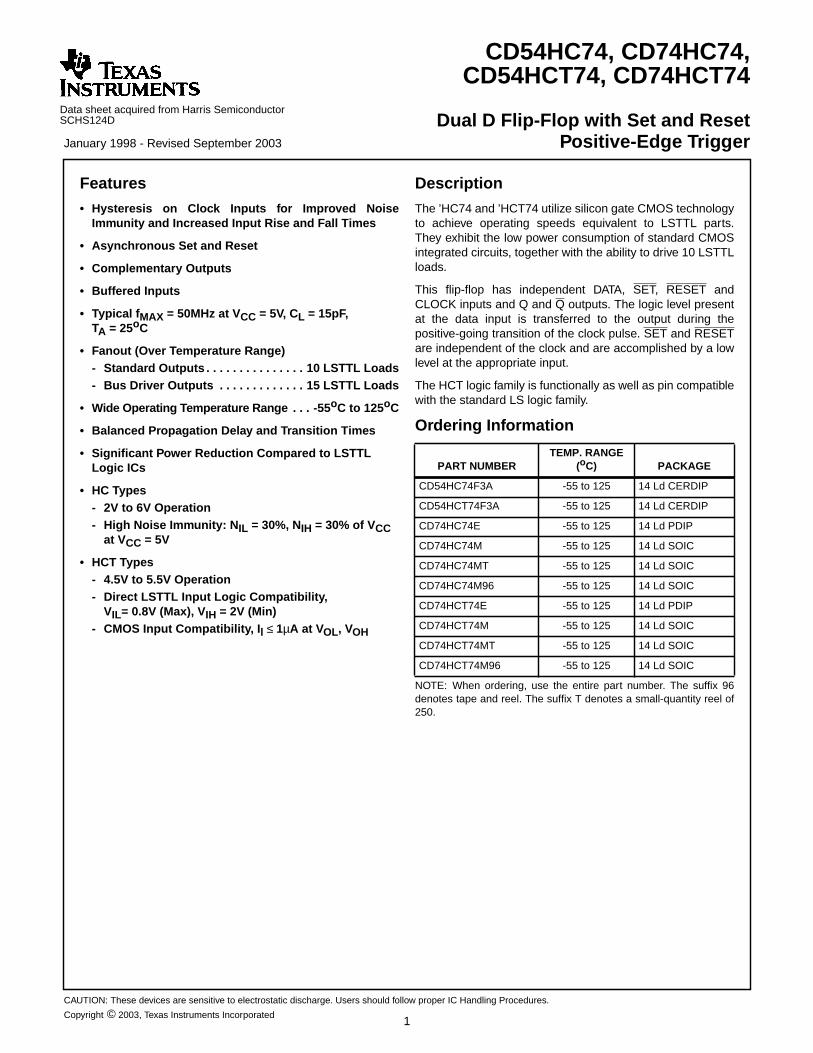
Data sheet acquired from Harris SemiconductorSCHS124D
Features
• Hysteresis on Clock Inputs for Improved NoiseImmunity and Increased Input Rise and Fall Times
• Asynchronous Set and Reset
• Complementary Outputs
• Buffered Inputs
• Typical fMAX = 50MHz at VCC = 5V, CL = 15pF,TA = 25oC
• Fanout (Over Temperature Range)- Standard Outputs . . . . . . . . . . . . . . . 10 LSTTL Loads- Bus Driver Outputs . . . . . . . . . . . . . 15 LSTTL Loads
• Wide Operating Temperature Range . . . -55oC to 125oC
• Balanced Propagation Delay and Transition Times
• Significant Power Reduction Compared to LSTTLLogic ICs
• HC Types- 2V to 6V Operation- High Noise Immunity: NIL = 30%, NIH = 30% of VCC
at VCC = 5V
• HCT Types- 4.5V to 5.5V Operation- Direct LSTTL Input Logic Compatibility,
VIL= 0.8V (Max), VIH = 2V (Min)- CMOS Input Compatibility, Il ≤ 1µA at VOL, VOH
Description
The ’HC74 and ’HCT74 utilize silicon gate CMOS technologyto achieve operating speeds equivalent to LSTTL parts.They exhibit the low power consumption of standard CMOSintegrated circuits, together with the ability to drive 10 LSTTLloads.
This flip-flop has independent DATA, SET, RESET andCLOCK inputs and Q and Q outputs. The logic level presentat the data input is transferred to the output during thepositive-going transition of the clock pulse. SET and RESETare independent of the clock and are accomplished by a lowlevel at the appropriate input.
The HCT logic family is functionally as well as pin compatiblewith the standard LS logic family.
Ordering Information
PART NUMBERTEMP. RANGE
(oC) PACKAGE
CD54HC74F3A -55 to 125 14 Ld CERDIP
CD54HCT74F3A -55 to 125 14 Ld CERDIP
CD74HC74E -55 to 125 14 Ld PDIP
CD74HC74M -55 to 125 14 Ld SOIC
CD74HC74MT -55 to 125 14 Ld SOIC
CD74HC74M96 -55 to 125 14 Ld SOIC
CD74HCT74E -55 to 125 14 Ld PDIP
CD74HCT74M -55 to 125 14 Ld SOIC
CD74HCT74MT -55 to 125 14 Ld SOIC
CD74HCT74M96 -55 to 125 14 Ld SOIC
NOTE: When ordering, use the entire part number. The suffix 96denotes tape and reel. The suffix T denotes a small-quantity reel of250.
CAUTION: These devices are sensitive to electrostatic discharge. Users should follow proper IC Handling Procedures.
Copyright © 2003, Texas Instruments Incorporated
CD54HC74, CD74HC74,CD54HCT74, CD74HCT74
Dual D Flip-Flop with Set and ResetPositive-Edge Trigger
[ /Title(CD54HC74,CD74HC74,CD74HCT74)/Subject(Dual DFlip-Flopwith Set
January 1998 - Revised September 2003
2
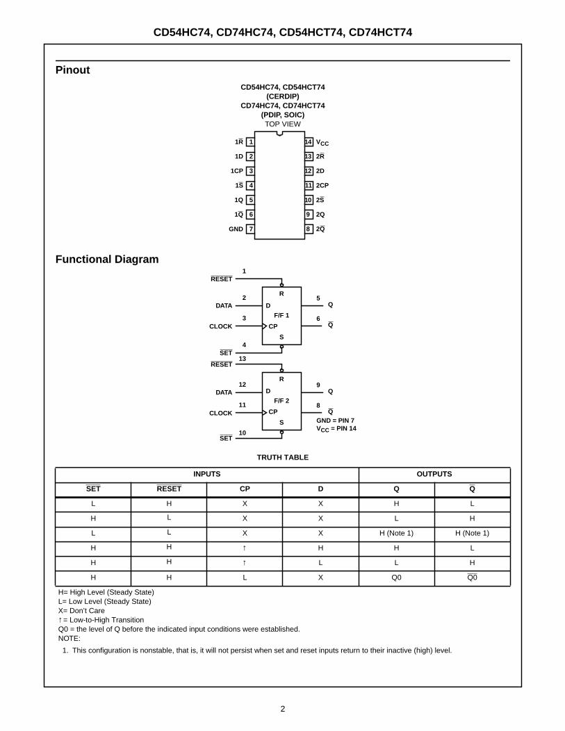
PinoutCD54HC74, CD54HCT74
(CERDIP)CD74HC74, CD74HCT74
(PDIP, SOIC)TOP VIEW
Functional Diagram
TRUTH TABLE
INPUTS OUTPUTS
SET RESET CP D Q Q
L H X X H L
H L X X L H
L L X X H (Note 1) H (Note 1)
H H ↑ H H L
H H ↑ L L H
H H L X Q0 Q0
H= High Level (Steady State)L= Low Level (Steady State)X= Don’t Care↑= Low-to-High TransitionQ0 = the level of Q before the indicated input conditions were established.NOTE:
1. This configuration is nonstable, that is, it will not persist when set and reset inputs return to their inactive (high) level.
1R
1D
1CP
1S
1Q
1Q
GND
VCC
2R
2D
2CP
2S
2Q
2Q
1
2
3
4
5
6
7
14
13
12
11
10
9
8
RESET
DATA
RESET
SET
1
2
3
13
5
6Q
Q
10
CLOCK
4SET
DATA12
11
9
8Q
Q
CLOCK
D
CP
R
F/F 2
S GND = PIN 7VCC = PIN 14
D
CP
R
F/F 1
S
CD54HC74, CD74HC74, CD54HCT74, CD74HCT74
3
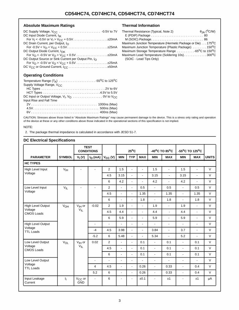
Absolute Maximum Ratings Thermal InformationDC Supply Voltage, VCC . . . . . . . . . . . . . . . . . . . . . . . . -0.5V to 7VDC Input Diode Current, IIK
For VI < -0.5V or VI > VCC + 0.5V . . . . . . . . . . . . . . . . . . . . . .±20mADC Drain Current, per Output, IO
For -0.5V < VO < VCC + 0.5V . . . . . . . . . . . . . . . . . . . . . . . . . .±25mADC Output Diode Current, IOK
For VO < -0.5V or VO > VCC + 0.5V . . . . . . . . . . . . . . . . . . . .±20mADC Output Source or Sink Current per Output Pin, IO
For VO > -0.5V or VO < VCC + 0.5V . . . . . . . . . . . . . . . . . . . .±25mADC VCC or Ground Current, ICC . . . . . . . . . . . . . . . . . . . . . . . . .±50mA
Operating ConditionsTemperature Range (TA) . . . . . . . . . . . . . . . . . . . . . -55oC to 125oCSupply Voltage Range, VCC
HC Types . . . . . . . . . . . . . . . . . . . . . . . . . . . . . . . . . . . . .2V to 6VHCT Types . . . . . . . . . . . . . . . . . . . . . . . . . . . . . . . . .4.5V to 5.5V
DC Input or Output Voltage, VI, VO . . . . . . . . . . . . . . . . . 0V to VCCInput Rise and Fall Time
2V . . . . . . . . . . . . . . . . . . . . . . . . . . . . . . . . . . . . . . 1000ns (Max)4.5V. . . . . . . . . . . . . . . . . . . . . . . . . . . . . . . . . . . . . . 500ns (Max)6V . . . . . . . . . . . . . . . . . . . . . . . . . . . . . . . . . . . . . . . 400ns (Max)
Thermal Resistance (Typical, Note 2) θJA (oC/W)E (PDIP) Package . . . . . . . . . . . . . . . . . . . . . . . . . . . . . . 80M (SOIC) Package. . . . . . . . . . . . . . . . . . . . . . . . . . . . . . 86
Maximum Junction Temperature (Hermetic Package or Die) . . . 175oCMaximum Junction Temperature (Plastic Package) . . . . . . . . 150oCMaximum Storage Temperature Range . . . . . . . . . .-65oC to 150oCMaximum Lead Temperature (Soldering 10s) . . . . . . . . . . . . . 300oC
(SOIC - Lead Tips Only)
CAUTION: Stresses above those listed in “Absolute Maximum Ratings” may cause permanent damage to the device. This is a stress only rating and operationof the device at these or any other conditions above those indicated in the operational sections of this specification is not implied.
NOTE:
2. The package thermal impedance is calculated in accordance with JESD 51-7.
DC Electrical Specifications
PARAMETER SYMBOL
TESTCONDITIONS
VCC (V)
25oC -40oC TO 85oC -55oC TO 125oC
UNITSVI (V) IO (mA) MIN TYP MAX MIN MAX MIN MAX
HC TYPES
High Level InputVoltage
VIH - - 2 1.5 - - 1.5 - 1.5 - V
4.5 3.15 - - 3.15 - 3.15 - V
6 4.2 - - 4.2 - 4.2 - V
Low Level InputVoltage
VIL - - 2 - - 0.5 - 0.5 - 0.5 V
4.5 - - 1.35 - 1.35 - 1.35 V
6 - - 1.8 - 1.8 - 1.8 V
High Level OutputVoltageCMOS Loads
VOH VIH orVIL
-0.02 2 1.9 - - 1.9 - 1.9 - V
4.5 4.4 - - 4.4 - 4.4 - V
6 5.9 - - 5.9 - 5.9 - V
High Level OutputVoltageTTL Loads
- - - - - - - - - V
-4 4.5 3.98 - - 3.84 - 3.7 - V
-5.2 6 5.48 - - 5.34 - 5.2 - V
Low Level OutputVoltageCMOS Loads
VOL VIH orVIL
0.02 2 - - 0.1 - 0.1 - 0.1 V
4.5 - - 0.1 - 0.1 - 0.1 V
6 - - 0.1 - 0.1 - 0.1 V
Low Level OutputVoltageTTL Loads
- - - - - - - - - V
4 4.5 - - 0.26 - 0.33 - 0.4 V
5.2 6 - - 0.26 - 0.33 - 0.4 V
Input LeakageCurrent
II VCC orGND
- 6 - - ±0.1 - ±1 - ±1 µA
CD54HC74, CD74HC74, CD54HCT74, CD74HCT74
4
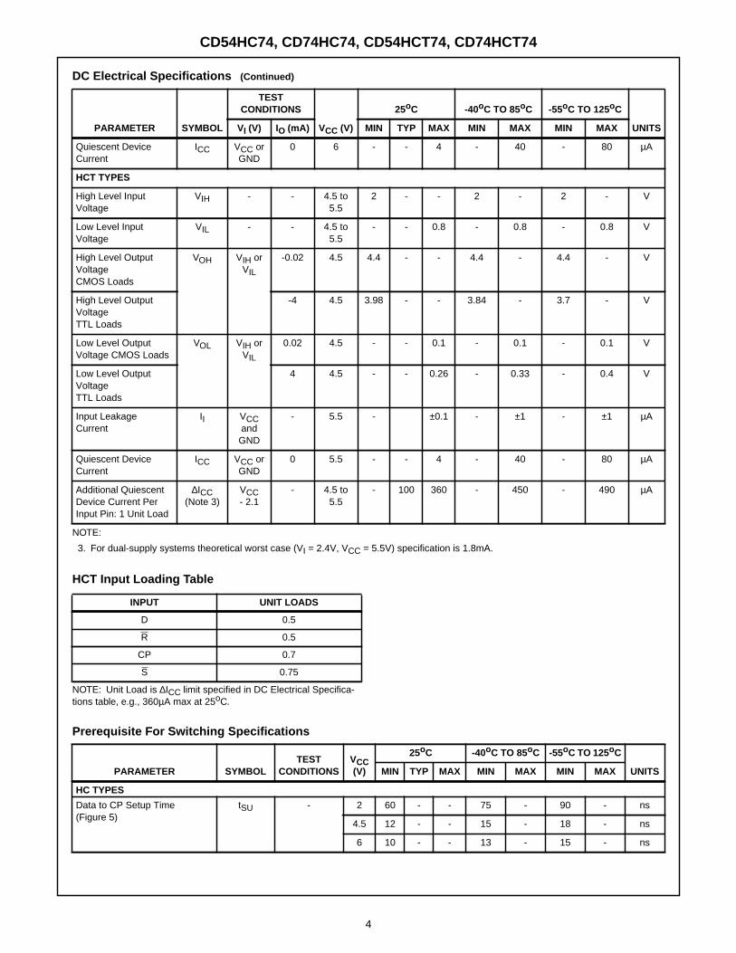
Quiescent DeviceCurrent
ICC VCC orGND
0 6 - - 4 - 40 - 80 µA
HCT TYPES
High Level InputVoltage
VIH - - 4.5 to5.5
2 - - 2 - 2 - V
Low Level InputVoltage
VIL - - 4.5 to5.5
- - 0.8 - 0.8 - 0.8 V
High Level OutputVoltageCMOS Loads
VOH VIH orVIL
-0.02 4.5 4.4 - - 4.4 - 4.4 - V
High Level OutputVoltageTTL Loads
-4 4.5 3.98 - - 3.84 - 3.7 - V
Low Level OutputVoltage CMOS Loads
VOL VIH orVIL
0.02 4.5 - - 0.1 - 0.1 - 0.1 V
Low Level OutputVoltageTTL Loads
4 4.5 - - 0.26 - 0.33 - 0.4 V
Input LeakageCurrent
II VCCandGND
- 5.5 - ±0.1 - ±1 - ±1 µA
Quiescent DeviceCurrent
ICC VCC orGND
0 5.5 - - 4 - 40 - 80 µA
Additional QuiescentDevice Current PerInput Pin: 1 Unit Load
∆ICC(Note 3)
VCC- 2.1
- 4.5 to5.5
- 100 360 - 450 - 490 µA
NOTE:
3. For dual-supply systems theoretical worst case (VI = 2.4V, VCC = 5.5V) specification is 1.8mA.
DC Electrical Specifications (Continued)
PARAMETER SYMBOL
TESTCONDITIONS
VCC (V)
25oC -40oC TO 85oC -55oC TO 125oC
UNITSVI (V) IO (mA) MIN TYP MAX MIN MAX MIN MAX
HCT Input Loading Table
INPUT UNIT LOADS
D 0.5
R 0.5
CP 0.7
S 0.75
NOTE: Unit Load is ∆ICC limit specified in DC Electrical Specifica-tions table, e.g., 360µA max at 25oC.
Prerequisite For Switching Specifications
PARAMETER SYMBOLTEST
CONDITIONSVCC(V)
25oC -40oC TO 85oC -55oC TO 125oC
UNITSMIN TYP MAX MIN MAX MIN MAX
HC TYPES
Data to CP Setup Time(Figure 5)
tSU - 2 60 - - 75 - 90 - ns
4.5 12 - - 15 - 18 - ns
6 10 - - 13 - 15 - ns
CD54HC74, CD74HC74, CD54HCT74, CD74HCT74
5
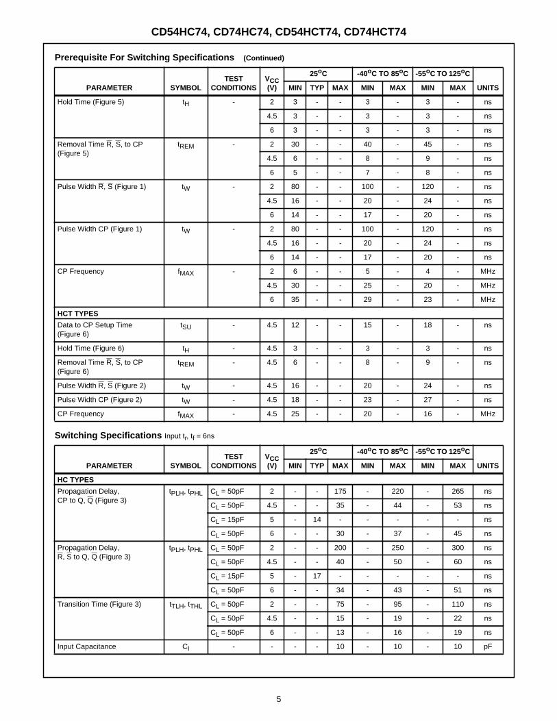
Hold Time (Figure 5) tH - 2 3 - - 3 - 3 - ns
4.5 3 - - 3 - 3 - ns
6 3 - - 3 - 3 - ns
Removal Time R, S, to CP(Figure 5)
tREM - 2 30 - - 40 - 45 - ns
4.5 6 - - 8 - 9 - ns
6 5 - - 7 - 8 - ns
Pulse Width R, S (Figure 1) tW - 2 80 - - 100 - 120 - ns
4.5 16 - - 20 - 24 - ns
6 14 - - 17 - 20 - ns
Pulse Width CP (Figure 1) tW - 2 80 - - 100 - 120 - ns
4.5 16 - - 20 - 24 - ns
6 14 - - 17 - 20 - ns
CP Frequency fMAX - 2 6 - - 5 - 4 - MHz
4.5 30 - - 25 - 20 - MHz
6 35 - - 29 - 23 - MHz
HCT TYPES
Data to CP Setup Time(Figure 6)
tSU - 4.5 12 - - 15 - 18 - ns
Hold Time (Figure 6) tH - 4.5 3 - - 3 - 3 - ns
Removal Time R, S, to CP(Figure 6)
tREM - 4.5 6 - - 8 - 9 - ns
Pulse Width R, S (Figure 2) tW - 4.5 16 - - 20 - 24 - ns
Pulse Width CP (Figure 2) tW - 4.5 18 - - 23 - 27 - ns
CP Frequency fMAX - 4.5 25 - - 20 - 16 - MHz
Switching Specifications Input tr, tf = 6ns
PARAMETER SYMBOLTEST
CONDITIONSVCC(V)
25oC -40oC TO 85oC -55oC TO 125oC
UNITSMIN TYP MAX MIN MAX MIN MAX
HC TYPES
Propagation Delay,CP to Q, Q (Figure 3)
tPLH, tPHL CL = 50pF 2 - - 175 - 220 - 265 ns
CL = 50pF 4.5 - - 35 - 44 - 53 ns
CL = 15pF 5 - 14 - - - - - ns
CL = 50pF 6 - - 30 - 37 - 45 ns
Propagation Delay,R, S to Q, Q (Figure 3)
tPLH, tPHL CL = 50pF 2 - - 200 - 250 - 300 ns
CL = 50pF 4.5 - - 40 - 50 - 60 ns
CL = 15pF 5 - 17 - - - - - ns
CL = 50pF 6 - - 34 - 43 - 51 ns
Transition Time (Figure 3) tTLH, tTHL CL = 50pF 2 - - 75 - 95 - 110 ns
CL = 50pF 4.5 - - 15 - 19 - 22 ns
CL = 50pF 6 - - 13 - 16 - 19 ns
Input Capacitance CI - - - - 10 - 10 - 10 pF
Prerequisite For Switching Specifications (Continued)
PARAMETER SYMBOLTEST
CONDITIONSVCC(V)
25oC -40oC TO 85oC -55oC TO 125oC
UNITSMIN TYP MAX MIN MAX MIN MAX
CD54HC74, CD74HC74, CD54HCT74, CD74HCT74
6
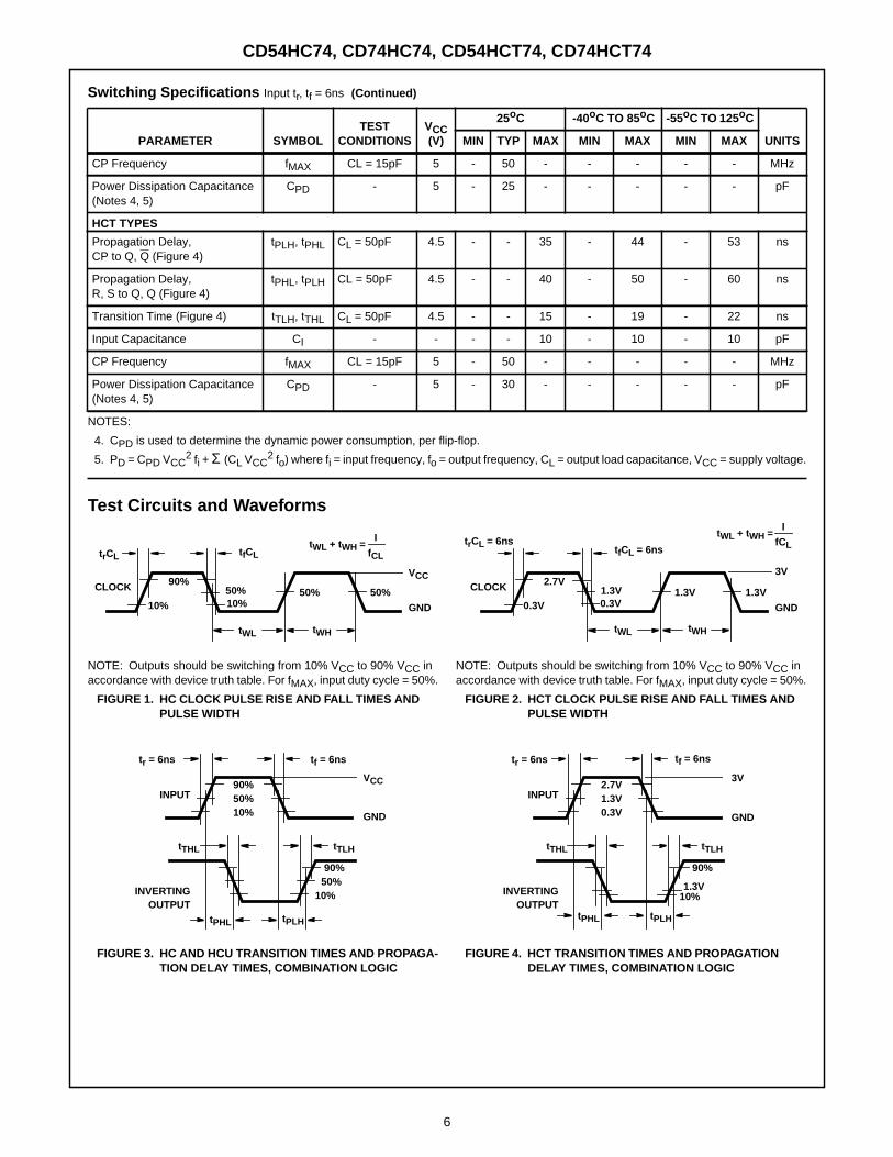
CP Frequency fMAX CL = 15pF 5 - 50 - - - - - MHz
Power Dissipation Capacitance(Notes 4, 5)
CPD - 5 - 25 - - - - - pF
HCT TYPES
Propagation Delay,CP to Q, Q (Figure 4)
tPLH, tPHL CL = 50pF 4.5 - - 35 - 44 - 53 ns
Propagation Delay,R, S to Q, Q (Figure 4)
tPHL, tPLH CL = 50pF 4.5 - - 40 - 50 - 60 ns
Transition Time (Figure 4) tTLH, tTHL CL = 50pF 4.5 - - 15 - 19 - 22 ns
Input Capacitance CI - - - - 10 - 10 - 10 pF
CP Frequency fMAX CL = 15pF 5 - 50 - - - - - MHz
Power Dissipation Capacitance(Notes 4, 5)
CPD - 5 - 30 - - - - - pF
NOTES:
4. CPD is used to determine the dynamic power consumption, per flip-flop.
5. PD = CPD VCC2 fi + Σ (CL VCC
2 fo) where fi = input frequency, fo = output frequency, CL = output load capacitance, VCC = supply voltage.
Switching Specifications Input tr, tf = 6ns (Continued)
PARAMETER SYMBOLTEST
CONDITIONSVCC(V)
25oC -40oC TO 85oC -55oC TO 125oC
UNITSMIN TYP MAX MIN MAX MIN MAX
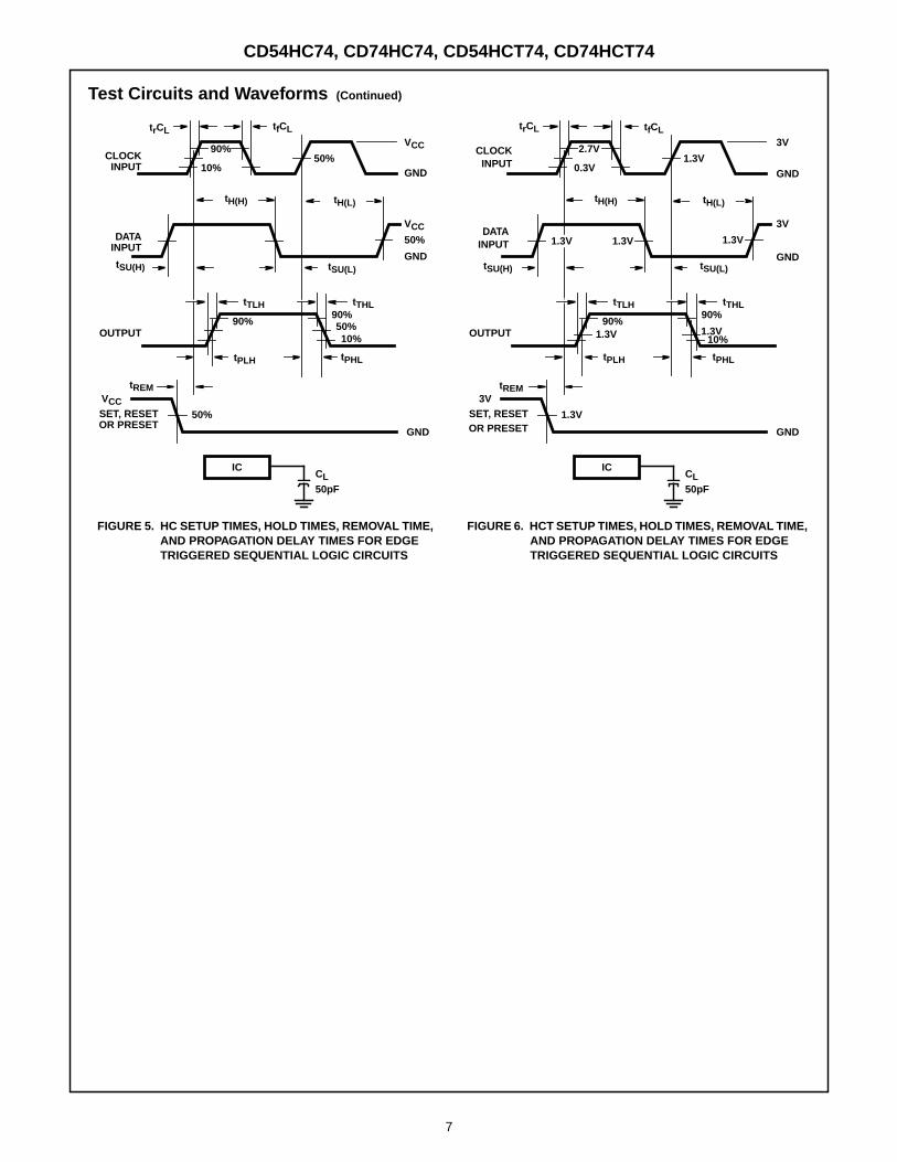
Test Circuits and Waveforms
NOTE: Outputs should be switching from 10% VCC to 90% VCC inaccordance with device truth table. For fMAX, input duty cycle = 50%.
FIGURE 1. HC CLOCK PULSE RISE AND FALL TIMES ANDPULSE WIDTH
NOTE: Outputs should be switching from 10% VCC to 90% VCC inaccordance with device truth table. For fMAX, input duty cycle = 50%.
FIGURE 2. HCT CLOCK PULSE RISE AND FALL TIMES ANDPULSE WIDTH
FIGURE 3. HC AND HCU TRANSITION TIMES AND PROPAGA-TION DELAY TIMES, COMBINATION LOGIC
FIGURE 4. HCT TRANSITION TIMES AND PROPAGATIONDELAY TIMES, COMBINATION LOGIC
CLOCK 90%50%
10% GND
VCC
trCL tfCL
50% 50%
tWL tWH
10%
tWL + tWH =fCL
I
CLOCK 2.7V1.3V
0.3V GND
3V
trCL = 6nstfCL = 6ns
1.3V 1.3V
tWL tWH
0.3V
tWL + tWH =fCL
I
tPHL tPLH
tTHL tTLH
90%50%10%
50%10%INVERTING
OUTPUT
INPUT
GND
VCC
tr = 6ns tf = 6ns
90%
tPHL tPLH
tTHL tTLH
2.7V1.3V0.3V
1.3V10%INVERTING
OUTPUT
INPUT
GND
3V
tr = 6ns tf = 6ns
90%
CD54HC74, CD74HC74, CD54HCT74, CD74HCT74
7
FIGURE 5. HC SETUP TIMES, HOLD TIMES, REMOVAL TIME,AND PROPAGATION DELAY TIMES FOR EDGETRIGGERED SEQUENTIAL LOGIC CIRCUITS
FIGURE 6. HCT SETUP TIMES, HOLD TIMES, REMOVAL TIME,AND PROPAGATION DELAY TIMES FOR EDGETRIGGERED SEQUENTIAL LOGIC CIRCUITS
Test Circuits and Waveforms (Continued)
trCL tfCL
GND
VCC
GND
VCC50%
90%
10%
GND
CLOCKINPUT
DATAINPUT
OUTPUT
SET, RESETOR PRESET
VCC50%
50%
90%
10%50%
90%
tREM
tPLH
tSU(H)
tTLH tTHL
tH(L)
tPHL
ICCL50pF
tSU(L)
tH(H)
trCL tfCL
GND
3V
GND
3V
1.3V2.7V
0.3V
GND
CLOCKINPUT
DATAINPUT
OUTPUT
SET, RESETOR PRESET
3V
1.3V
1.3V1.3V
90%
10%1.3V
90%
tREM
tPLH
tSU(H)
tTLH tTHL
tH(L)
tPHL
ICCL50pF
tSU(L)
1.3V
tH(H)
1.3V
CD54HC74, CD74HC74, CD54HCT74, CD74HCT74
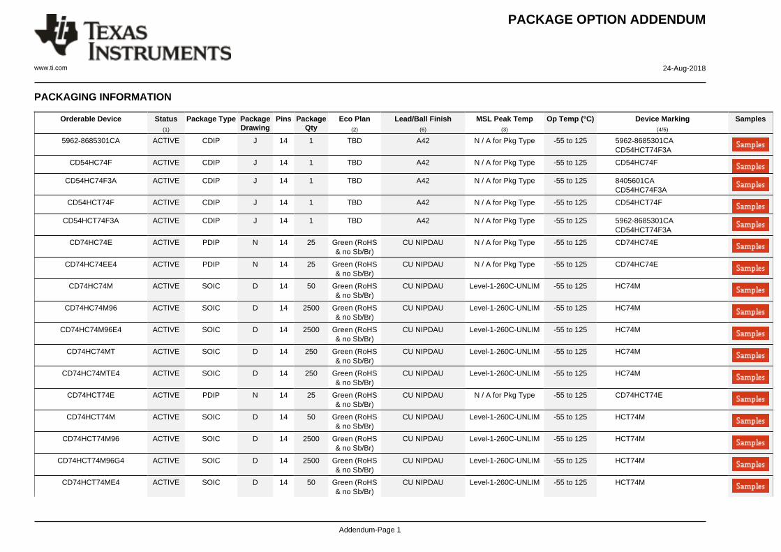
PACKAGE OPTION ADDENDUM
www.ti.com 24-Aug-2018
Addendum-Page 1
PACKAGING INFORMATION
Orderable Device Status(1)
Package Type PackageDrawing
Pins PackageQty
Eco Plan(2)
Lead/Ball Finish(6)
MSL Peak Temp(3)
Op Temp (°C) Device Marking(4/5)
Samples
5962-8685301CA ACTIVE CDIP J 14 1 TBD A42 N / A for Pkg Type -55 to 125 5962-8685301CACD54HCT74F3A
CD54HC74F ACTIVE CDIP J 14 1 TBD A42 N / A for Pkg Type -55 to 125 CD54HC74F
CD54HC74F3A ACTIVE CDIP J 14 1 TBD A42 N / A for Pkg Type -55 to 125 8405601CACD54HC74F3A
CD54HCT74F ACTIVE CDIP J 14 1 TBD A42 N / A for Pkg Type -55 to 125 CD54HCT74F
CD54HCT74F3A ACTIVE CDIP J 14 1 TBD A42 N / A for Pkg Type -55 to 125 5962-8685301CACD54HCT74F3A
CD74HC74E ACTIVE PDIP N 14 25 Green (RoHS& no Sb/Br)
CU NIPDAU N / A for Pkg Type -55 to 125 CD74HC74E
CD74HC74EE4 ACTIVE PDIP N 14 25 Green (RoHS& no Sb/Br)
CU NIPDAU N / A for Pkg Type -55 to 125 CD74HC74E
CD74HC74M ACTIVE SOIC D 14 50 Green (RoHS& no Sb/Br)
CU NIPDAU Level-1-260C-UNLIM -55 to 125 HC74M
CD74HC74M96 ACTIVE SOIC D 14 2500 Green (RoHS& no Sb/Br)
CU NIPDAU Level-1-260C-UNLIM -55 to 125 HC74M
CD74HC74M96E4 ACTIVE SOIC D 14 2500 Green (RoHS& no Sb/Br)
CU NIPDAU Level-1-260C-UNLIM -55 to 125 HC74M
CD74HC74MT ACTIVE SOIC D 14 250 Green (RoHS& no Sb/Br)
CU NIPDAU Level-1-260C-UNLIM -55 to 125 HC74M
CD74HC74MTE4 ACTIVE SOIC D 14 250 Green (RoHS& no Sb/Br)
CU NIPDAU Level-1-260C-UNLIM -55 to 125 HC74M
CD74HCT74E ACTIVE PDIP N 14 25 Green (RoHS& no Sb/Br)
CU NIPDAU N / A for Pkg Type -55 to 125 CD74HCT74E
CD74HCT74M ACTIVE SOIC D 14 50 Green (RoHS& no Sb/Br)
CU NIPDAU Level-1-260C-UNLIM -55 to 125 HCT74M
CD74HCT74M96 ACTIVE SOIC D 14 2500 Green (RoHS& no Sb/Br)
CU NIPDAU Level-1-260C-UNLIM -55 to 125 HCT74M
CD74HCT74M96G4 ACTIVE SOIC D 14 2500 Green (RoHS& no Sb/Br)
CU NIPDAU Level-1-260C-UNLIM -55 to 125 HCT74M
CD74HCT74ME4 ACTIVE SOIC D 14 50 Green (RoHS& no Sb/Br)
CU NIPDAU Level-1-260C-UNLIM -55 to 125 HCT74M
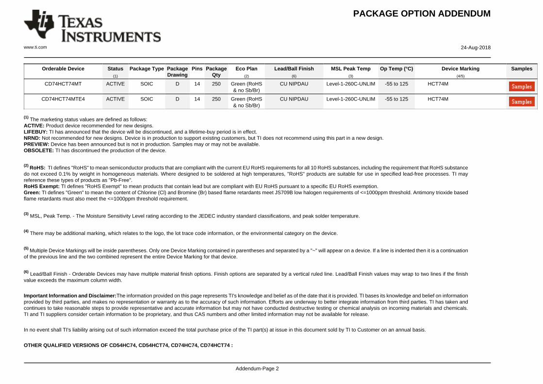
PACKAGE OPTION ADDENDUM
www.ti.com 24-Aug-2018
Addendum-Page 2
Orderable Device Status(1)
Package Type PackageDrawing
Pins PackageQty
Eco Plan(2)
Lead/Ball Finish(6)
MSL Peak Temp(3)
Op Temp (°C) Device Marking(4/5)
Samples
CD74HCT74MT ACTIVE SOIC D 14 250 Green (RoHS& no Sb/Br)
CU NIPDAU Level-1-260C-UNLIM -55 to 125 HCT74M
CD74HCT74MTE4 ACTIVE SOIC D 14 250 Green (RoHS& no Sb/Br)
CU NIPDAU Level-1-260C-UNLIM -55 to 125 HCT74M
(1) The marketing status values are defined as follows:ACTIVE: Product device recommended for new designs.LIFEBUY: TI has announced that the device will be discontinued, and a lifetime-buy period is in effect.NRND: Not recommended for new designs. Device is in production to support existing customers, but TI does not recommend using this part in a new design.PREVIEW: Device has been announced but is not in production. Samples may or may not be available.OBSOLETE: TI has discontinued the production of the device.
(2) RoHS: TI defines "RoHS" to mean semiconductor products that are compliant with the current EU RoHS requirements for all 10 RoHS substances, including the requirement that RoHS substancedo not exceed 0.1% by weight in homogeneous materials. Where designed to be soldered at high temperatures, "RoHS" products are suitable for use in specified lead-free processes. TI mayreference these types of products as "Pb-Free".RoHS Exempt: TI defines "RoHS Exempt" to mean products that contain lead but are compliant with EU RoHS pursuant to a specific EU RoHS exemption.Green: TI defines "Green" to mean the content of Chlorine (Cl) and Bromine (Br) based flame retardants meet JS709B low halogen requirements of <=1000ppm threshold. Antimony trioxide basedflame retardants must also meet the <=1000ppm threshold requirement.
(3) MSL, Peak Temp. - The Moisture Sensitivity Level rating according to the JEDEC industry standard classifications, and peak solder temperature.
(4) There may be additional marking, which relates to the logo, the lot trace code information, or the environmental category on the device.
(5) Multiple Device Markings will be inside parentheses. Only one Device Marking contained in parentheses and separated by a "~" will appear on a device. If a line is indented then it is a continuationof the previous line and the two combined represent the entire Device Marking for that device.
(6) Lead/Ball Finish - Orderable Devices may have multiple material finish options. Finish options are separated by a vertical ruled line. Lead/Ball Finish values may wrap to two lines if the finishvalue exceeds the maximum column width.
Important Information and Disclaimer:The information provided on this page represents TI's knowledge and belief as of the date that it is provided. TI bases its knowledge and belief on informationprovided by third parties, and makes no representation or warranty as to the accuracy of such information. Efforts are underway to better integrate information from third parties. TI has taken andcontinues to take reasonable steps to provide representative and accurate information but may not have conducted destructive testing or chemical analysis on incoming materials and chemicals.TI and TI suppliers consider certain information to be proprietary, and thus CAS numbers and other limited information may not be available for release.
In no event shall TI's liability arising out of such information exceed the total purchase price of the TI part(s) at issue in this document sold by TI to Customer on an annual basis.
OTHER QUALIFIED VERSIONS OF CD54HC74, CD54HCT74, CD74HC74, CD74HCT74 :
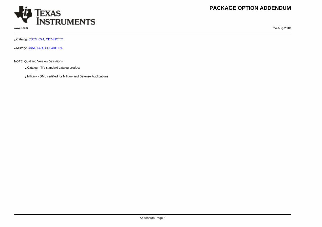
PACKAGE OPTION ADDENDUM
www.ti.com 24-Aug-2018
Addendum-Page 3
• Catalog: CD74HC74, CD74HCT74
• Military: CD54HC74, CD54HCT74
NOTE: Qualified Version Definitions:
• Catalog - TI's standard catalog product
• Military - QML certified for Military and Defense Applications
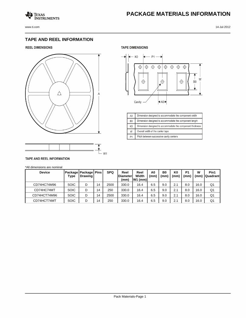
TAPE AND REEL INFORMATION
*All dimensions are nominal
Device PackageType
PackageDrawing
Pins SPQ ReelDiameter
(mm)
ReelWidth
W1 (mm)
A0(mm)
B0(mm)
K0(mm)
P1(mm)
W(mm)
Pin1Quadrant
CD74HC74M96 SOIC D 14 2500 330.0 16.4 6.5 9.0 2.1 8.0 16.0 Q1
CD74HC74MT SOIC D 14 250 330.0 16.4 6.5 9.0 2.1 8.0 16.0 Q1
CD74HCT74M96 SOIC D 14 2500 330.0 16.4 6.5 9.0 2.1 8.0 16.0 Q1
CD74HCT74MT SOIC D 14 250 330.0 16.4 6.5 9.0 2.1 8.0 16.0 Q1
PACKAGE MATERIALS INFORMATION
www.ti.com 14-Jul-2012
Pack Materials-Page 1
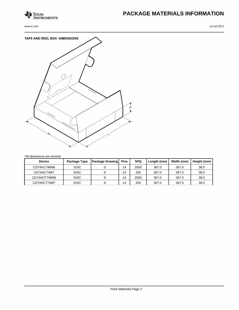
*All dimensions are nominal
Device Package Type Package Drawing Pins SPQ Length (mm) Width (mm) Height (mm)
CD74HC74M96 SOIC D 14 2500 367.0 367.0 38.0
CD74HC74MT SOIC D 14 250 367.0 367.0 38.0
CD74HCT74M96 SOIC D 14 2500 367.0 367.0 38.0
CD74HCT74MT SOIC D 14 250 367.0 367.0 38.0
PACKAGE MATERIALS INFORMATION
www.ti.com 14-Jul-2012
Pack Materials-Page 2
www.ti.com
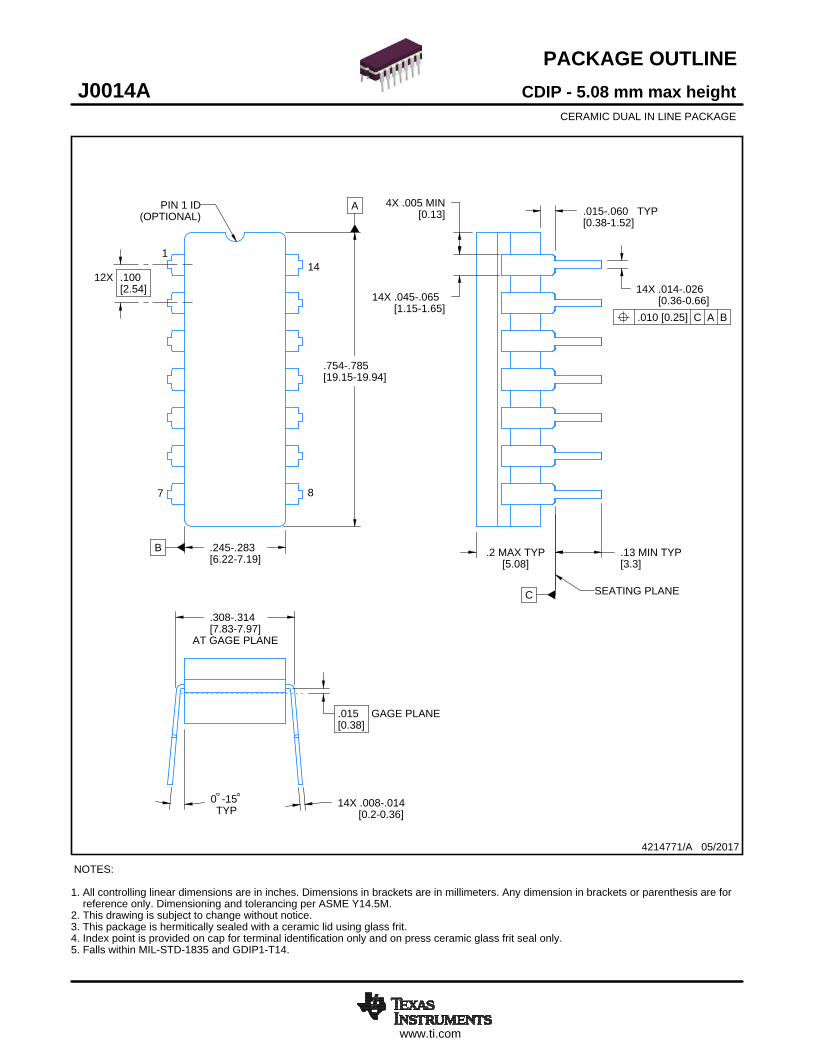
PACKAGE OUTLINE
C
14X .008-.014 [0.2-0.36]TYP
-150
AT GAGE PLANE
-.314.308-7.977.83[ ]
14X -.026.014-0.660.36[ ]14X -.065.045
-1.651.15[ ]
.2 MAX TYP[5.08]
.13 MIN TYP[3.3]
TYP-.060.015-1.520.38[ ]
4X .005 MIN[0.13]
12X .100[2.54]
.015 GAGE PLANE[0.38]
A
-.785.754-19.9419.15[ ]
B -.283.245-7.196.22[ ]
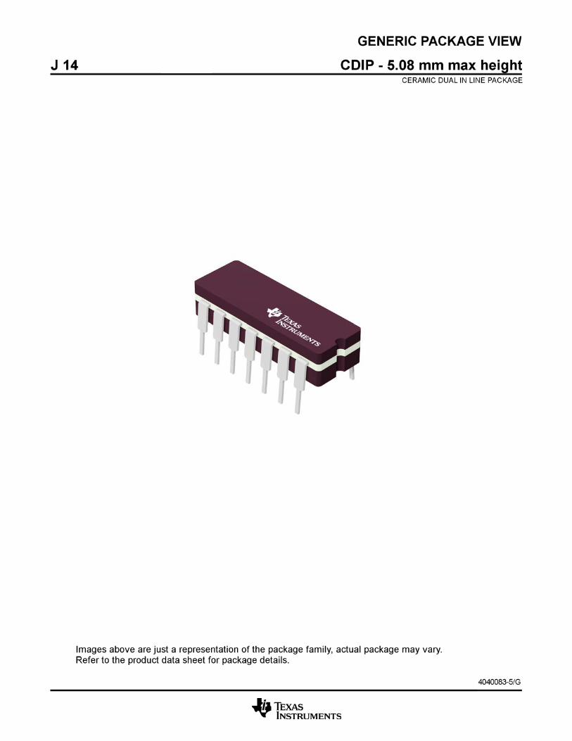
CDIP - 5.08 mm max heightJ0014ACERAMIC DUAL IN LINE PACKAGE
4214771/A 05/2017
NOTES: 1. All controlling linear dimensions are in inches. Dimensions in brackets are in millimeters. Any dimension in brackets or parenthesis are for reference only. Dimensioning and tolerancing per ASME Y14.5M.2. This drawing is subject to change without notice. 3. This package is hermitically sealed with a ceramic lid using glass frit.4. Index point is provided on cap for terminal identification only and on press ceramic glass frit seal only.5. Falls within MIL-STD-1835 and GDIP1-T14.
7 8
141
PIN 1 ID(OPTIONAL)
SCALE 0.900
SEATING PLANE
.010 [0.25] C A B
www.ti.com
EXAMPLE BOARD LAYOUT
ALL AROUND[0.05]
MAX.002
.002 MAX[0.05]ALL AROUND
SOLDER MASKOPENING
METAL
(.063)[1.6]
(R.002 ) TYP[0.05]
14X ( .039)[1]
( .063)[1.6]
12X (.100 )[2.54]
(.300 ) TYP[7.62]
CDIP - 5.08 mm max heightJ0014ACERAMIC DUAL IN LINE PACKAGE
4214771/A 05/2017
LAND PATTERN EXAMPLENON-SOLDER MASK DEFINED
SCALE: 5X
SEE DETAIL A SEE DETAIL B
SYMM
SYMM
1
7 8
14
DETAIL ASCALE: 15X
SOLDER MASKOPENING
METAL
DETAIL B13X, SCALE: 15X
IMPORTANT NOTICE
Texas Instruments Incorporated (TI) reserves the right to make corrections, enhancements, improvements and other changes to itssemiconductor products and services per JESD46, latest issue, and to discontinue any product or service per JESD48, latest issue. Buyersshould obtain the latest relevant information before placing orders and should verify that such information is current and complete.TI’s published terms of sale for semiconductor products (http://www.ti.com/sc/docs/stdterms.htm) apply to the sale of packaged integratedcircuit products that TI has qualified and released to market. Additional terms may apply to the use or sale of other types of TI products andservices.Reproduction of significant portions of TI information in TI data sheets is permissible only if reproduction is without alteration and isaccompanied by all associated warranties, conditions, limitations, and notices. TI is not responsible or liable for such reproduceddocumentation. Information of third parties may be subject to additional restrictions. Resale of TI products or services with statementsdifferent from or beyond the parameters stated by TI for that product or service voids all express and any implied warranties for theassociated TI product or service and is an unfair and deceptive business practice. TI is not responsible or liable for any such statements.Buyers and others who are developing systems that incorporate TI products (collectively, “Designers”) understand and agree that Designersremain responsible for using their independent analysis, evaluation and judgment in designing their applications and that Designers havefull and exclusive responsibility to assure the safety of Designers' applications and compliance of their applications (and of all TI productsused in or for Designers’ applications) with all applicable regulations, laws and other applicable requirements. Designer represents that, withrespect to their applications, Designer has all the necessary expertise to create and implement safeguards that (1) anticipate dangerousconsequences of failures, (2) monitor failures and their consequences, and (3) lessen the likelihood of failures that might cause harm andtake appropriate actions. Designer agrees that prior to using or distributing any applications that include TI products, Designer willthoroughly test such applications and the functionality of such TI products as used in such applications.TI’s provision of technical, application or other design advice, quality characterization, reliability data or other services or information,including, but not limited to, reference designs and materials relating to evaluation modules, (collectively, “TI Resources”) are intended toassist designers who are developing applications that incorporate TI products; by downloading, accessing or using TI Resources in anyway, Designer (individually or, if Designer is acting on behalf of a company, Designer’s company) agrees to use any particular TI Resourcesolely for this purpose and subject to the terms of this Notice.TI’s provision of TI Resources does not expand or otherwise alter TI’s applicable published warranties or warranty disclaimers for TIproducts, and no additional obligations or liabilities arise from TI providing such TI Resources. TI reserves the right to make corrections,enhancements, improvements and other changes to its TI Resources. TI has not conducted any testing other than that specificallydescribed in the published documentation for a particular TI Resource.Designer is authorized to use, copy and modify any individual TI Resource only in connection with the development of applications thatinclude the TI product(s) identified in such TI Resource. NO OTHER LICENSE, EXPRESS OR IMPLIED, BY ESTOPPEL OR OTHERWISETO ANY OTHER TI INTELLECTUAL PROPERTY RIGHT, AND NO LICENSE TO ANY TECHNOLOGY OR INTELLECTUAL PROPERTYRIGHT OF TI OR ANY THIRD PARTY IS GRANTED HEREIN, including but not limited to any patent right, copyright, mask work right, orother intellectual property right relating to any combination, machine, or process in which TI products or services are used. Informationregarding or referencing third-party products or services does not constitute a license to use such products or services, or a warranty orendorsement thereof. Use of TI Resources may require a license from a third party under the patents or other intellectual property of thethird party, or a license from TI under the patents or other intellectual property of TI.TI RESOURCES ARE PROVIDED “AS IS” AND WITH ALL FAULTS. TI DISCLAIMS ALL OTHER WARRANTIES ORREPRESENTATIONS, EXPRESS OR IMPLIED, REGARDING RESOURCES OR USE THEREOF, INCLUDING BUT NOT LIMITED TOACCURACY OR COMPLETENESS, TITLE, ANY EPIDEMIC FAILURE WARRANTY AND ANY IMPLIED WARRANTIES OFMERCHANTABILITY, FITNESS FOR A PARTICULAR PURPOSE, AND NON-INFRINGEMENT OF ANY THIRD PARTY INTELLECTUALPROPERTY RIGHTS. TI SHALL NOT BE LIABLE FOR AND SHALL NOT DEFEND OR INDEMNIFY DESIGNER AGAINST ANY CLAIM,INCLUDING BUT NOT LIMITED TO ANY INFRINGEMENT CLAIM THAT RELATES TO OR IS BASED ON ANY COMBINATION OFPRODUCTS EVEN IF DESCRIBED IN TI RESOURCES OR OTHERWISE. IN NO EVENT SHALL TI BE LIABLE FOR ANY ACTUAL,DIRECT, SPECIAL, COLLATERAL, INDIRECT, PUNITIVE, INCIDENTAL, CONSEQUENTIAL OR EXEMPLARY DAMAGES INCONNECTION WITH OR ARISING OUT OF TI RESOURCES OR USE THEREOF, AND REGARDLESS OF WHETHER TI HAS BEENADVISED OF THE POSSIBILITY OF SUCH DAMAGES.Unless TI has explicitly designated an individual product as meeting the requirements of a particular industry standard (e.g., ISO/TS 16949and ISO 26262), TI is not responsible for any failure to meet such industry standard requirements.Where TI specifically promotes products as facilitating functional safety or as compliant with industry functional safety standards, suchproducts are intended to help enable customers to design and create their own applications that meet applicable functional safety standardsand requirements. Using products in an application does not by itself establish any safety features in the application. Designers mustensure compliance with safety-related requirements and standards applicable to their applications. Designer may not use any TI products inlife-critical medical equipment unless authorized officers of the parties have executed a special contract specifically governing such use.Life-critical medical equipment is medical equipment where failure of such equipment would cause serious bodily injury or death (e.g., lifesupport, pacemakers, defibrillators, heart pumps, neurostimulators, and implantables). Such equipment includes, without limitation, allmedical devices identified by the U.S. Food and Drug Administration as Class III devices and equivalent classifications outside the U.S.TI may expressly designate certain products as completing a particular qualification (e.g., Q100, Military Grade, or Enhanced Product).Designers agree that it has the necessary expertise to select the product with the appropriate qualification designation for their applicationsand that proper product selection is at Designers’ own risk. Designers are solely responsible for compliance with all legal and regulatoryrequirements in connection with such selection.Designer will fully indemnify TI and its representatives against any damages, costs, losses, and/or liabilities arising out of Designer’s non-compliance with the terms and provisions of this Notice.
Mailing Address: Texas Instruments, Post Office Box 655303, Dallas, Texas 75265Copyright © 2018, Texas Instruments Incorporated