Embed Size (px)
Citation preview

UNIVERSITY OF OSLODepartment of Informatics
Carry-Look-AheadAdder inMultiple-ValuedRecharge Logic
Cand. Scient. Thesis
Vidar StrønstadØverås
May 2005


Acknowledgements.
This thesis concludes my work for the Candidatus Scientiarum degree inMicroelectronic Systems at the Department of Informatics, University ofOslo. My work was initiated in February 2003, and concluded May 2005.
I would like to thank my supervisor Yngvar Berg for accepting me ashis student, for guidance and useful discussions. Furthermore I wouldlike to pay tribute to Dag T. Wisland, Mats E. Høvin and Omid Mirmota-hari for their assistance.
Next I would like to thank Espen Torstensen, Johannes Goplen Loms-dalen, Rene Jensen, Øivind Næss, Snorre Aunet, Olav Stanly Kyrvestad,Kjetil Meisal and Claus Limbodal for their contributions to this thesis,and also my fellow students at the laboratory, for scientific discussionsand coffee breaks.
Last but not least, I would like to thank my family for their uncondi-tional support and help, and Lena, for her patience, and understanding.Your support has been invaluable.
i

ii
Abstract
In the last few decades, multiple-valued logics have been proposed as apossible alternative or enrichment to binary logic. Multiple-valued cir-cuits replace the two states of binary logics with finite or infinite sets ofvalues.
Many multiple-valued circuits, both current-mode and voltage-mode,have been published. To the best of our knowledge very few of thesehave had commercial success. However, multiple-valued recharge lo-gics show great potential, reducing the number of transistors neededto perform a logic operation considerably when compared to binary lo-gic. Present multiple-valued recharge adders use an inefficient carry-handling, and thus setting limitations of the number of bits that can berepresented, as well as the max operation frequency. In this thesis amultiple-valued recharge adder making use of carry-look-ahead (CLA)is presented, addressing the carry-ripple problem. Furthermore, thepresented multiple-valued CLA recharge adder is used in a proposed16-bit CLA scheme. The CLA scheme is compared to a 16-bit multiple-valued recharge adder, regarding gate-delay, maximum operation fre-quency, and power consumption. Limitations of the proposed design isalso presented.
iii

iv

CONTENTS
Contents
Acknowledgements i
Abstract iii
1 Introduction 1
1.1 Introduction . . . . . . . . . . . . . . . . . . . . . . . . . . . . . . 1
1.2 Overview of the thesis. . . . . . . . . . . . . . . . . . . . . . . . 3
2 Recharge Logic 5
2.1 The floating-gate inverter . . . . . . . . . . . . . . . . . . . . . 5
2.2 The multiple-valued semi-floating-gate latch . . . . . . . . . . 7
2.3 The capacitor . . . . . . . . . . . . . . . . . . . . . . . . . . . . . 10
2.4 Binary-to-recharge-binary-converter . . . . . . . . . . . . . . . 11
2.5 Binary-to-multiple-valued-converter and Multiple-valued-to-binary-converter . . . . . . . . . . . . . . . . . . . . . . . . . . . 12
2.6 Adder . . . . . . . . . . . . . . . . . . . . . . . . . . . . . . . . . . 15
2.7 Summary . . . . . . . . . . . . . . . . . . . . . . . . . . . . . . . . 20
3 The multiple-valued Carry Look Ahead Adder 21
3.1 The Prototype Carry-Look-Ahead Full-Adder . . . . . . . . . . 21
3.2 Prototype adder used in cascade . . . . . . . . . . . . . . . . . 33
3.3 Carry-Look-Ahead Scheme . . . . . . . . . . . . . . . . . . . . . 36
3.4 The MV CLA adder used in the CLA scheme . . . . . . . . . . 38
3.5 Summary . . . . . . . . . . . . . . . . . . . . . . . . . . . . . . . . 43
4 System Considerations 45
4.1 Sources of malfunction . . . . . . . . . . . . . . . . . . . . . . . 45
4.2 Clock Frequency . . . . . . . . . . . . . . . . . . . . . . . . . . . 48
4.3 Power consumption . . . . . . . . . . . . . . . . . . . . . . . . . 49
4.4 The prototype design . . . . . . . . . . . . . . . . . . . . . . . . 52
4.5 Summary . . . . . . . . . . . . . . . . . . . . . . . . . . . . . . . . 54
v
CONTENTS
5 Conclusion and proposal for further work 575.1 Main contributions . . . . . . . . . . . . . . . . . . . . . . . . . 575.2 Experimental Results . . . . . . . . . . . . . . . . . . . . . . . . 575.3 Further work . . . . . . . . . . . . . . . . . . . . . . . . . . . . . 58
A Truth tables 59
B Complete CLA proposal 61B.1 A complete 16-bit MV CLA full-adder . . . . . . . . . . . . . . 61
C Transistor tables 65
D Instruments and Pin-out overview 67D.1 Test Setup . . . . . . . . . . . . . . . . . . . . . . . . . . . . . . . 67D.2 Pin-out overview . . . . . . . . . . . . . . . . . . . . . . . . . . . 68
E Additional Figures 71
F Matlab scripts 75F.1 Scripts . . . . . . . . . . . . . . . . . . . . . . . . . . . . . . . . . 75
G Additional Simulations 83
H Glossary 93
Bibliography 95
List of figures 104
List of tables 105
vi

Chapter 1
Introduction
1.1 Introduction
Binary logic has been the preferred logic for a long time. Like any otherlogic, binary logic has its advantages and disadvantages. The advantagesare mainly accuracy and speed. The frequencies have increased as thetransistor sizes have been downscaled. This, on the other hand, hasincreased the heat radiation caused by the transistors. Another problemis that today, internal routing occupies most of the chip area, as thenumber of transistors increase.
It is now understood and accepted that the limit for transistor size oneday will be reached. When that time comes, binary logics will presentfew, if any, options on how to increase performance, as the number oftransistors on a single chip will come to a stand still.
Multiple-valued logics (MVL) on the other hand offers the possibility torepresent more than two logic values on a single line. Thus meaning thatmore operations can be carried out using fewer transistors. A resultof this is that logic circuits that radiate far less heat can be designed.Many of the multiple-value floating gate circuits can not operate at thefrequencies that binary logics operates on, but they compensate for this,by representing m logic values on a single line.
While MVL has a long history in literature, the big breakthrough consid-ering industry has yet to come. MVL is most commonly used in memorydesigns, but this may change when transistor sizes reach a minimum.
Most of the proposed MV solutions are based on current-mode lo-gics. The current-mode approach consumes significant power, due tostatic currents for each logic level. This has switched the attention to
1
1.1. INTRODUCTION
voltage-mode multiple-valued logics. The voltage-mode approach, con-structed using CMOS offers a design with less power consumption thanthe current-mode approach. Furthermore, voltage-mode MV full-addershave also been designed, and while using far less transistors than theirbinary counterparts, a need for better carry signal handling is addressed.The carry propagation of MV ripple adders restricts the operation fre-quency and the number of bits that can be represented. This again lim-its the circuits where adders are used. A MV ripple adder used in e.g. adecimator, limits both the operation frequency and the number of bitsthat can be represented. Therefore a solution to these problems hasbeen addressed.
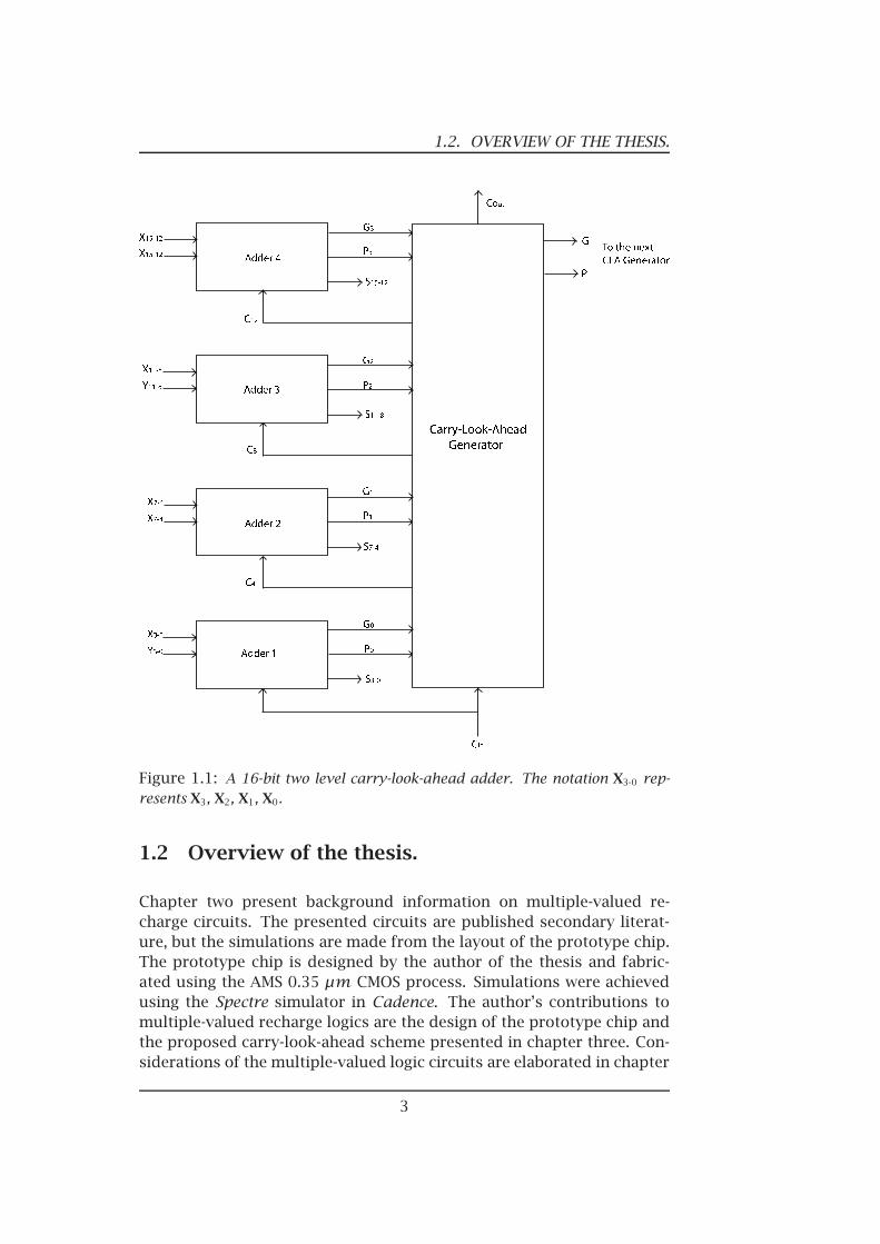
The scheme most commonly used for accelerating carry-propagation iscalled the carry-look-ahead (CLA) scheme [1]. The main idea of thisscheme is to generate all incoming carries in parallel, an thus avoid wait-ing until the correct carry propagates from the adder where it has beengenerated. Figure 1.1 illustrates the basic idea of CLA. By implementinga MV adder using a CLA scheme, the delay of carry propagation will bereduced. This will lead to the opportunity to increase both the operationfrequency and the number of bits that can be represented. This againwill lead to an increase in performance for circuits using these adders.
All carry handling is carried out in the Carry-Look-Ahead Generator. Gi
represents the internally-generated-carry signals. These signals do notdepend on an external carry-in, only the original inputs. Pi on the otherhand represents the sum where carry-out is 0 but where an externalcarry-in will trigger a carry-propagation. Gi and Pi are calculated in par-allel, before an eventual carry-in is introduced.
CLA adders have been implemented using different approaches andtechnologies [2–6]. Also, a MV CLA adder designed in a 0.35 µm process,capable of operating at 400MHz has been reported [7]. The motivationfor this thesis was to implement a voltage-mode multiple-valued semi-floating-gate adder using a carry-look-ahead scheme. The multiple-valuefloating gate CLA adder will be compared to the multiple-value float-ing gate full adder, in regard of gate-delay, max operation frequency,power-delay product and energy-delay product. Comments will also bemade regarding the power consumption of the multiple-value floatinggate Carry-Look-Ahead adder. For the solution designed for this thesis,summation is handled using multiple-valued signals. This results in ananalog approach regarding the summation. One of the main reasonsfor this approach is that it has a more even use of power than binarysolutions, which again results in a power effective solution. The carryhandling on the other hand is carried out, using binary signals and bin-ary gates, for fast shifting and propagation.
2
1.2. OVERVIEW OF THE THESIS.
Figure 1.1: A 16-bit two level carry-look-ahead adder. The notation X3-0 rep-resents X3, X2, X1, X0.
1.2 Overview of the thesis.
Chapter two present background information on multiple-valued re-charge circuits. The presented circuits are published secondary literat-ure, but the simulations are made from the layout of the prototype chip.The prototype chip is designed by the author of the thesis and fabric-ated using the AMS 0.35 µm CMOS process. Simulations were achievedusing the Spectre simulator in Cadence. The author’s contributions tomultiple-valued recharge logics are the design of the prototype chip andthe proposed carry-look-ahead scheme presented in chapter three. Con-siderations of the multiple-valued logic circuits are elaborated in chapter
3

1.2. OVERVIEW OF THE THESIS.
four. Chapter five presents the conclusions and proposals for furtherwork.
A listed outline of the thesis:
• Chapter 1 gives a brief summary for the motivation of the thesis.
• Chapter 2 presents the basic multiple-valued building blocks theprototype system is based upon. Also presented, is the MV Full-Adder.
• Chapter 3 gives a thorough presentation of the MV Carry-Look-Ahead Adder. Furthermore a proposed carry-look-ahead schemeoffers a great improvement over the MV full-adder consideringgate-delay and frequency.
• Chapter 4 includes considerations to the multiple-valued logics.
• Chapter 5 presents a discussion and proposals for further work.
4
Chapter 2
Recharge Logic
In this chapter the basic circuits that are used throughoutthe thesis are introduced. Demonstrations on how they areconstructed, and illustrations of their functionality is alsoprovided. A full-adder based upon the basic circuits is alsointroduced. Further more, since multiple-valued logics needan interface that can communicate with existing binary sys-tems, circuits that can translate binary to multiple-valued andvice versa are introduced.
2.1 The floating-gate inverter
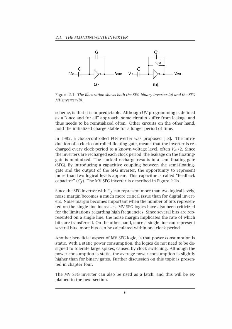
The idea of using capacitive coupled inputs on a FG-inverter was intro-duced in 1992 by Shibata [8–10]. This FG-inverter has later been knownas the neuron-MOSFET, since it resembles the behaviour of the “neurons”in a living body [11].
The floating-gate (FG) inverter [12] is composed using standard MOS-transistors and capacitors, as presented in Figure 2.1a. The input signalof an FG inverter is capacitive coupled, as opposed to a binary inverter.For this reason the FG inverter can have M input signals. Using inputsthat are capacitive coupled, means that the output is calculated by thevoltage on the floating-gate. A small change on the floating-gate, willresult in a large voltage change on the output of the inverter. With Minput signals, the voltage on the floating-gate represents several inputsignals, as will be described later.
In order to obtain a consistent and desired function, the FG circuits needto be initialized or programmed. On a local scale, the ultra-violet (UV)FG inverter has been the object of much research [13–17]. The UV FG in-verter is programmed using ultra violet light. The downside with the UV
5
2.1. THE FLOATING-GATE INVERTER
Figure 2.1: The Illustration shows both the SFG binary inverter (a) and the SFGMV inverter (b).
scheme, is that it is unpredictable. Although UV programming is definedas a “once and for all” approach, some circuits suffer from leakage andthus needs to be reinitialized often. Other circuits on the other hand,hold the initialized charge stable for a longer period of time.
In 1992, a clock-controlled FG-inverter was proposed [18]. The intro-duction of a clock-controlled floating-gate, means that the inverter is re-charged every clock-period to a known voltage level, often Vdd/2. Sincethe inverters are recharged each clock period, the leakage on the floating-gate is minimized. The clocked recharge results in a semi-floating-gate(SFG). By introducing a capacitive coupling between the semi-floating-gate and the output of the SFG inverter, the opportunity to representmore than two logical levels appear. This capacitor is called “feedbackcapacitor” (Cf ). The MV SFG inverter is described in Figure 2.1b.
Since the SFG inverter with Cf can represent more than two logical levels,noise margin becomes a much more critical issue than for digital invert-ers. Noise margin becomes important when the number of bits represen-ted on the single line increases. MV SFG logics have also been criticizedfor the limitations regarding high frequencies. Since several bits are rep-resented on a single line, the noise margin implicates the rate of whichbits are transferred. On the other hand, since a single line can representseveral bits, more bits can be calculated within one clock period.
Another beneficial aspect of MV SFG logic, is that power consumption isstatic. With a static power consumption, the logics do not need to be de-signed to tolerate large spikes, caused by clock switching. Although thepower consumption is static, the average power consumption is slightlyhigher than for binary gates. Further discussion on this topic is presen-ted in chapter four.
The MV SFG inverter can also be used as a latch, and this will be ex-plained in the next section.
6
2.2. THE MULTIPLE-VALUED SEMI-FLOATING-GATE LATCH
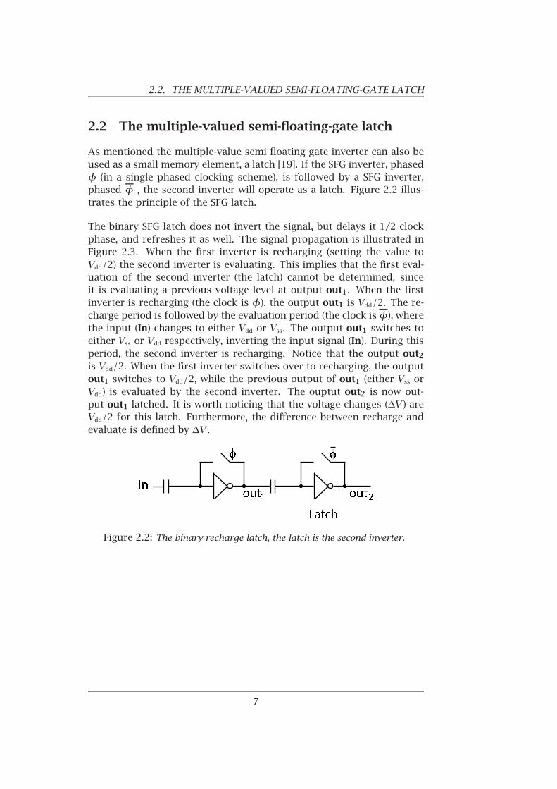
2.2 The multiple-valued semi-floating-gate latch
As mentioned the multiple-value semi floating gate inverter can also beused as a small memory element, a latch [19]. If the SFG inverter, phasedφ (in a single phased clocking scheme), is followed by a SFG inverter,phased φ , the second inverter will operate as a latch. Figure 2.2 illus-trates the principle of the SFG latch.
The binary SFG latch does not invert the signal, but delays it 1/2 clockphase, and refreshes it as well. The signal propagation is illustrated inFigure 2.3. When the first inverter is recharging (setting the value toVdd/2) the second inverter is evaluating. This implies that the first eval-uation of the second inverter (the latch) cannot be determined, sinceit is evaluating a previous voltage level at output out1. When the firstinverter is recharging (the clock is φ), the output out1 is Vdd/2. The re-charge period is followed by the evaluation period (the clock isφ), wherethe input (In) changes to either Vdd or Vss. The output out1 switches toeither Vss or Vdd respectively, inverting the input signal (In). During thisperiod, the second inverter is recharging. Notice that the output out2
is Vdd/2. When the first inverter switches over to recharging, the outputout1 switches to Vdd/2, while the previous output of out1 (either Vss orVdd) is evaluated by the second inverter. The ouptut out2 is now out-put out1 latched. It is worth noticing that the voltage changes (∆V ) areVdd/2 for this latch. Furthermore, the difference between recharge andevaluate is defined by ∆V .
Figure 2.2: The binary recharge latch, the latch is the second inverter.
7
2.2. THE MULTIPLE-VALUED SEMI-FLOATING-GATE LATCH
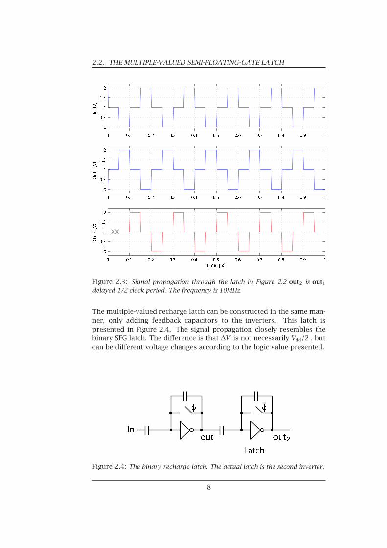
Figure 2.3: Signal propagation through the latch in Figure 2.2 out2 is out1
delayed 1/2 clock period. The frequency is 10MHz.
The multiple-valued recharge latch can be constructed in the same man-ner, only adding feedback capacitors to the inverters. This latch ispresented in Figure 2.4. The signal propagation closely resembles thebinary SFG latch. The difference is that ∆V is not necessarily Vdd/2 , butcan be different voltage changes according to the logic value presented.
Figure 2.4: The binary recharge latch. The actual latch is the second inverter.
8

2.2. THE MULTIPLE-VALUED SEMI-FLOATING-GATE LATCH
The gain of the multiple-valued recharge inverter can be given by theequation
G = CiCf + Cgd + CT
A(2.1)
Where Ci is the capacitor coupled to the input, Cf the feedback capacitor,Cgd the gate-drain capacitance, CT the total capacitance and A is givenby
A = gmgo
(2.2)
In an inverter based amplifier, A is negative, thus leading to G beingnegative. Furthermore, given that
A→ ∞ (2.3)
And also givenCdg → 0 (2.4)
This will leave the following simplified equation of G
G = CiCf
(2.5)
Furthermore, to be able to move the negative value out of G, the absolutevalue of the original equation of G is used. The original equation is usedfor a more correct representation of G
G =⏐⏐⏐⏐⏐
CiCf + Cgd + CT
A
⏐⏐⏐⏐⏐ (2.6)
This equation can be used to illustrate Figure 2.4. Now, given that theprevious circuit to the first inverter is clocked φ, Out1 can be expressed
Out1(n) = −G1 · In(n) (2.7)
This leads toOut2(n+ 1) = G2 ·Out1(n) (2.8)
These expressions lead to
Out2(n) = −G1 ·G2 · In(n− 1) (2.9)
In this thesis, a one phased clocking scheme is used, and the circuitsare therefore sensitive to clock skew. The gain of the circuits is alsosensitive to the value of A. The smaller A is, the smaller the gain. Asmall value of A, can imply that the value of go is large, due to channellength modulation, also called Early effect. This can be caused by shorttransistors.
The presented MV latch has also been proposed used to implement staticmemory cells [20]. Furthermore, a multiple-valued static-static memoryhas been proposed for synaptic storage [21] [22].
9
2.3. THE CAPACITOR
2.3 The capacitor
The most important components of the presented circuits are the capa-citors, therefore it is important to take a look at some of the possibleimplementation solutions. Capacitances can be extracted between al-most any layer and doped area, in different degrees. The overlappingarea can be calculated with the formula C = ε ·A/d. In this formula ε isthe dielectric constant for the oxide between the layers, A is the overlaparea of the layers, and d is the distance between the layers.
There are different ways to implement capacitances, although only a fewwill be mentioned here. For this thesis the first solution presented hasbeen used. The reason for this, is that this solution presents the leastcomplicated modules. The other solutions are mentioned to present anoverview over other approaches.
1) Interpoly capacitor: A capacitor is implemented using two layers ofpolysilicon on top of each other. Many MOS technologies that are used toimplement analog circuits have two layers of polysilicon [23].
2) Finger capacitor: Depends on the design rules for each individual pro-cess. It is typically used in the absence of a double-poly process, and isconstructed by poly and metal layers. The 0.12µ STM process can bementioned as an example of processes using this technique. In this pro-cess, capacitors are designed using metal 1, 2, 3, 4, 5 and 6, together withactive and poly. The metal layers are fingered to increase the capacitance.
3) Coupled capacitance: A coupling capacitance is usually seen as a para-sitic capacitance. Coupling capacitance is either the result of two layersinteracting, fringing capacitance, or a result of two different layers cross-ing, with the thick oxide separating the layers.
To minimize the effect of nonlinearity and parasitic capacitances,stable, well matched capacitors are needed. As the radix (logic levels) in-creases, this becomes even more important. When using multiple-valuedlogics, it is important to implement large enough capacitors to preventdomination of non-linearity and parasitic capacitances.
10
2.4. BINARY-TO-RECHARGE-BINARY-CONVERTER
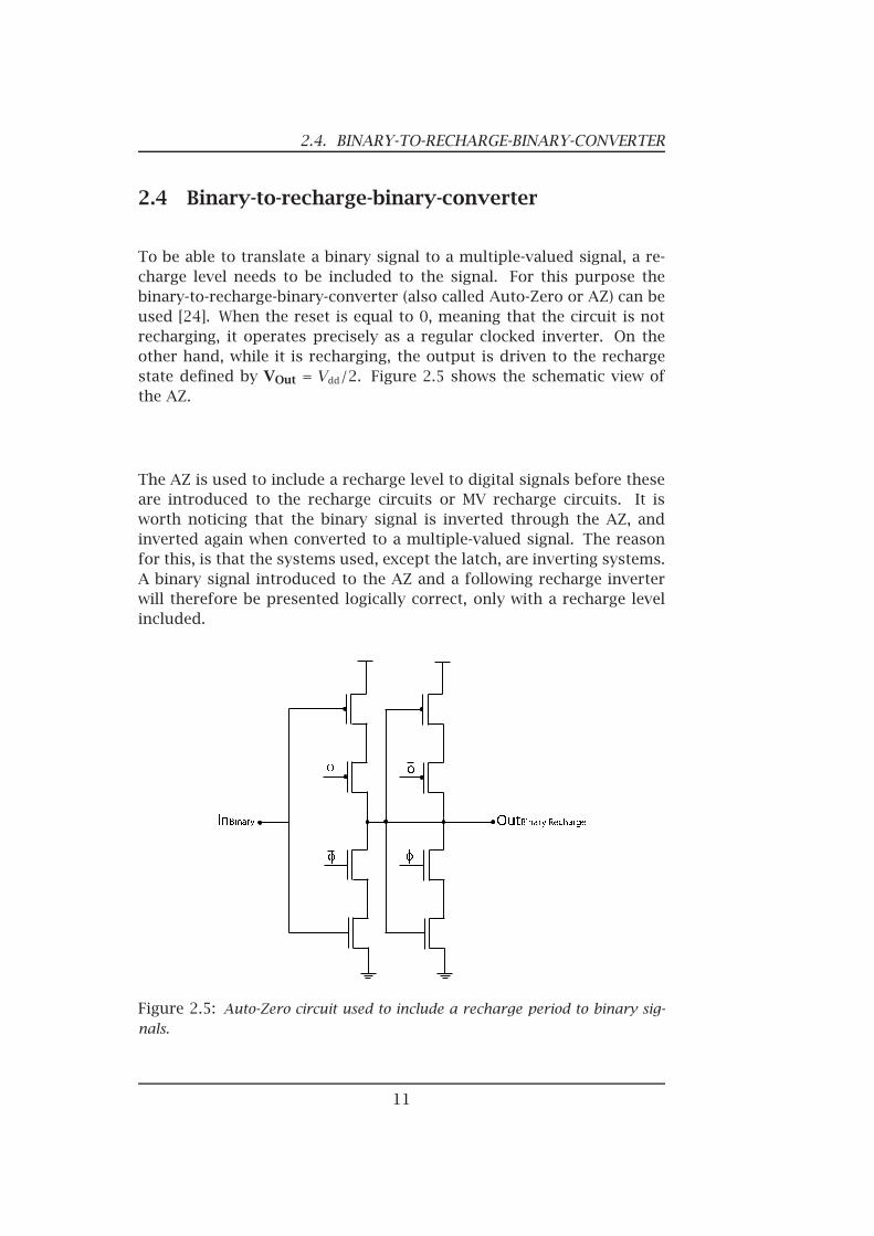
2.4 Binary-to-recharge-binary-converter
To be able to translate a binary signal to a multiple-valued signal, a re-charge level needs to be included to the signal. For this purpose thebinary-to-recharge-binary-converter (also called Auto-Zero or AZ) can beused [24]. When the reset is equal to 0, meaning that the circuit is notrecharging, it operates precisely as a regular clocked inverter. On theother hand, while it is recharging, the output is driven to the rechargestate defined by VOut = Vdd/2. Figure 2.5 shows the schematic view ofthe AZ.
The AZ is used to include a recharge level to digital signals before theseare introduced to the recharge circuits or MV recharge circuits. It isworth noticing that the binary signal is inverted through the AZ, andinverted again when converted to a multiple-valued signal. The reasonfor this, is that the systems used, except the latch, are inverting systems.A binary signal introduced to the AZ and a following recharge inverterwill therefore be presented logically correct, only with a recharge levelincluded.
Figure 2.5: Auto-Zero circuit used to include a recharge period to binary sig-nals.
11
2.5. BINARY-TO-MULTIPLE-VALUED-CONVERTER ANDMULTIPLE-VALUED-TO-BINARY-CONVERTER
2.5 Binary-to-multiple-valued-converter and Multiple-valued-to-binary-converter
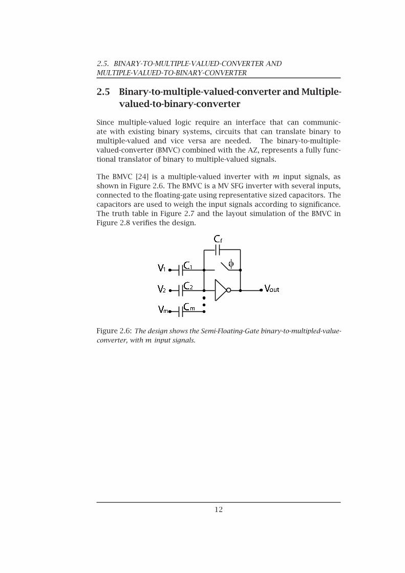
Since multiple-valued logic require an interface that can communic-ate with existing binary systems, circuits that can translate binary tomultiple-valued and vice versa are needed. The binary-to-multiple-valued-converter (BMVC) combined with the AZ, represents a fully func-tional translator of binary to multiple-valued signals.
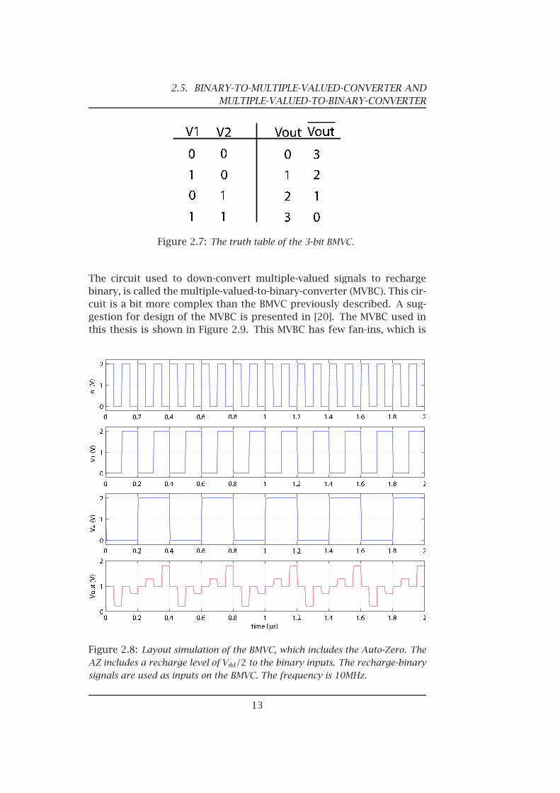
The BMVC [24] is a multiple-valued inverter with m input signals, asshown in Figure 2.6. The BMVC is a MV SFG inverter with several inputs,connected to the floating-gate using representative sized capacitors. Thecapacitors are used to weigh the input signals according to significance.The truth table in Figure 2.7 and the layout simulation of the BMVC inFigure 2.8 verifies the design.
Figure 2.6: The design shows the Semi-Floating-Gate binary-to-multipled-value-converter, with m input signals.
12
2.5. BINARY-TO-MULTIPLE-VALUED-CONVERTER ANDMULTIPLE-VALUED-TO-BINARY-CONVERTER
Figure 2.7: The truth table of the 3-bit BMVC.
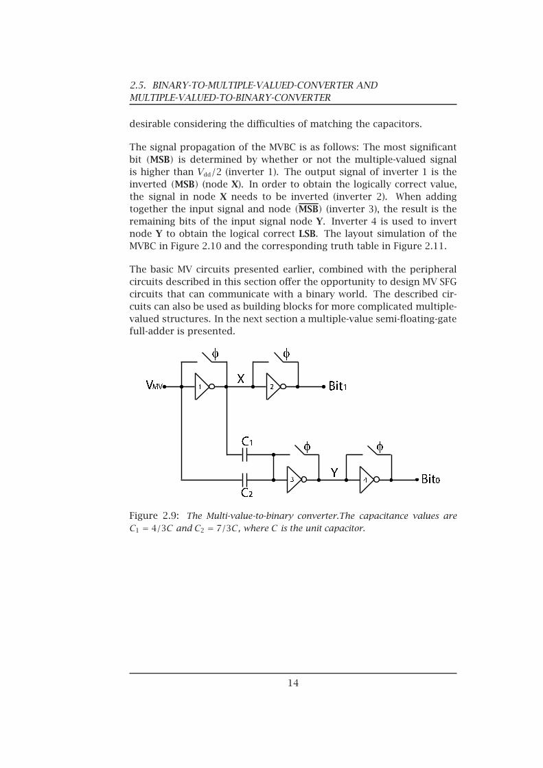
The circuit used to down-convert multiple-valued signals to rechargebinary, is called the multiple-valued-to-binary-converter (MVBC). This cir-cuit is a bit more complex than the BMVC previously described. A sug-gestion for design of the MVBC is presented in [20]. The MVBC used inthis thesis is shown in Figure 2.9. This MVBC has few fan-ins, which is
Figure 2.8: Layout simulation of the BMVC, which includes the Auto-Zero. TheAZ includes a recharge level of Vdd/2 to the binary inputs. The recharge-binarysignals are used as inputs on the BMVC. The frequency is 10MHz.
13
2.5. BINARY-TO-MULTIPLE-VALUED-CONVERTER ANDMULTIPLE-VALUED-TO-BINARY-CONVERTER
desirable considering the difficulties of matching the capacitors.
The signal propagation of the MVBC is as follows: The most significantbit (MSB) is determined by whether or not the multiple-valued signalis higher than Vdd/2 (inverter 1). The output signal of inverter 1 is theinverted (MSB) (node X). In order to obtain the logically correct value,the signal in node X needs to be inverted (inverter 2). When addingtogether the input signal and node (MSB) (inverter 3), the result is theremaining bits of the input signal node Y. Inverter 4 is used to invertnode Y to obtain the logical correct LSB. The layout simulation of theMVBC in Figure 2.10 and the corresponding truth table in Figure 2.11.
The basic MV circuits presented earlier, combined with the peripheralcircuits described in this section offer the opportunity to design MV SFGcircuits that can communicate with a binary world. The described cir-cuits can also be used as building blocks for more complicated multiple-valued structures. In the next section a multiple-value semi-floating-gatefull-adder is presented.
Figure 2.9: The Multi-value-to-binary converter.The capacitance values areC1 = 4/3C and C2 = 7/3C, where C is the unit capacitor.
14

2.6. ADDER
Figure 2.10: Simulation of layout, showing how the MVBC operates. The R4 in-put results in two a two-bit output, the output bits are represented with separatewires. In this simulation the carry in is logic 0. The frequency is 10MHz.
2.6 Adder
Like most full-adders, the MV full-adder has three input signals, e.g. Xi,Yi and Ci, and two output signals, e.g. Co and Sum. The multiple valuedsignals to be summed are represented by Xi and Yi while Ci representsthe carry-in. The output signal Sum represents, as the name suggests,the sum, while Co represents the carry-out of the adder. The radix of Co
Figure 2.11: The truth table of the 2-bit MVBC.
15
2.6. ADDER
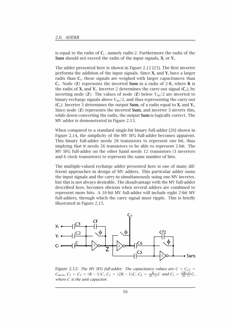
is equal to the radix of Ci , namely radix-2. Furthermore the radix of theSum should not exceed the radix of the input signals, Xi or Yi.
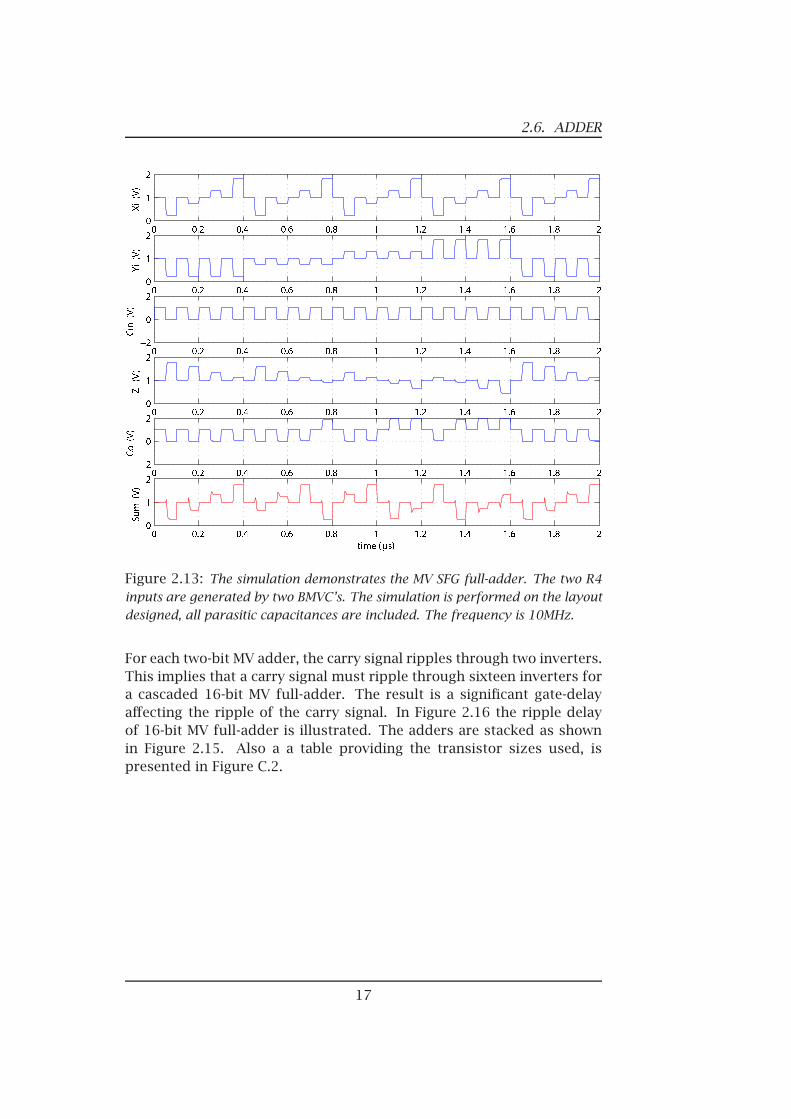
The adder presented here is shown in Figure 2.12 [25]. The first inverterperforms the addition of the input signals. Since Xi and Yi have a largerradix than Ci, these signals are weighed with larger capacitances thanCi. Node (Z) represents the inverted Sum in a radix of 2-R, where R isthe radix of Xi and Yi. Inverter 2 determines the carry-out signal (Co), byinverting node (Z). The values of node (Z) below Vdd/2 are inverted tobinary-recharge signals above Vdd/2, and thus representing the carry-out(Co). Inverter 3 determines the output Sum, of a radix equal to Xi and Yi.Since node (Z) represents the inverted Sum, and inverter 3 inverts this,while down-converting the radix, the output Sum is logically correct. TheMV adder is demonstrated in Figure 2.13.
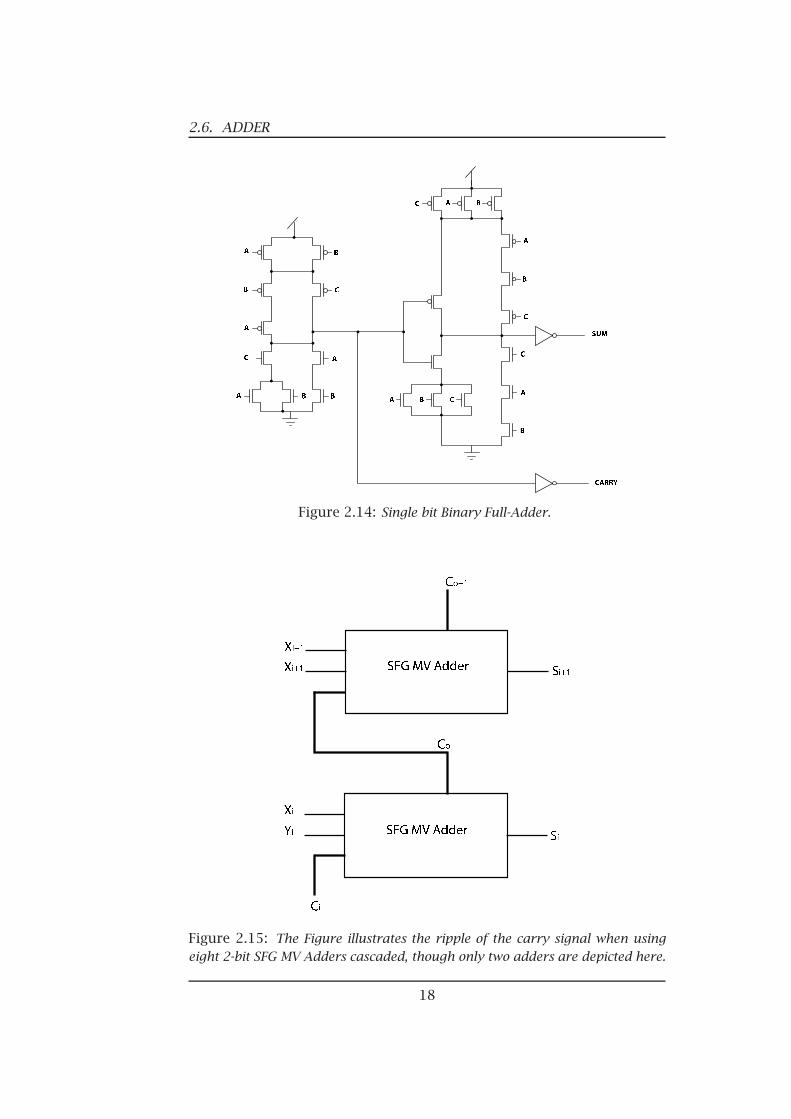
When compared to a standard single-bit binary full-adder [26] shown inFigure 2.14, the simplicity of the MV SFG full-adder becomes apparent.This binary full-adder needs 28 transistors to represent one bit, thusimplying that it needs 56 transistors to be able to represent 2-bit. TheMV SFG full-adder on the other hand needs 12 transistors (3 invertersand 6 clock transistors) to represent the same number of bits.
The multiple-valued recharge adder presented here is one of many dif-ferent approaches in design of MV adders. This particular adder sumsthe input signals and the carry-in simultaneously using one MV inverter,but this is not always desirable. The disadvantage with the MV full-adderdescribed here, becomes obvious when several adders are combined torepresent more bits. A 16-bit MV full-adder will include eight 2-bit MVfull-adders, through which the carry signal must ripple. This is brieflyillustrated in Figure 2.15.
Figure 2.12: The MV SFG full-adder. The capacitance values are C = Cf2 =Cmin, C2 = C3 = (R − 1)C, Cf = (2R − 1)C, C6 = R
(R−1)C and C5 = (2R−1)(R−1) C,
where C is the unit capacitor.
16
2.6. ADDER
Figure 2.13: The simulation demonstrates the MV SFG full-adder. The two R4inputs are generated by two BMVC’s. The simulation is performed on the layoutdesigned, all parasitic capacitances are included. The frequency is 10MHz.
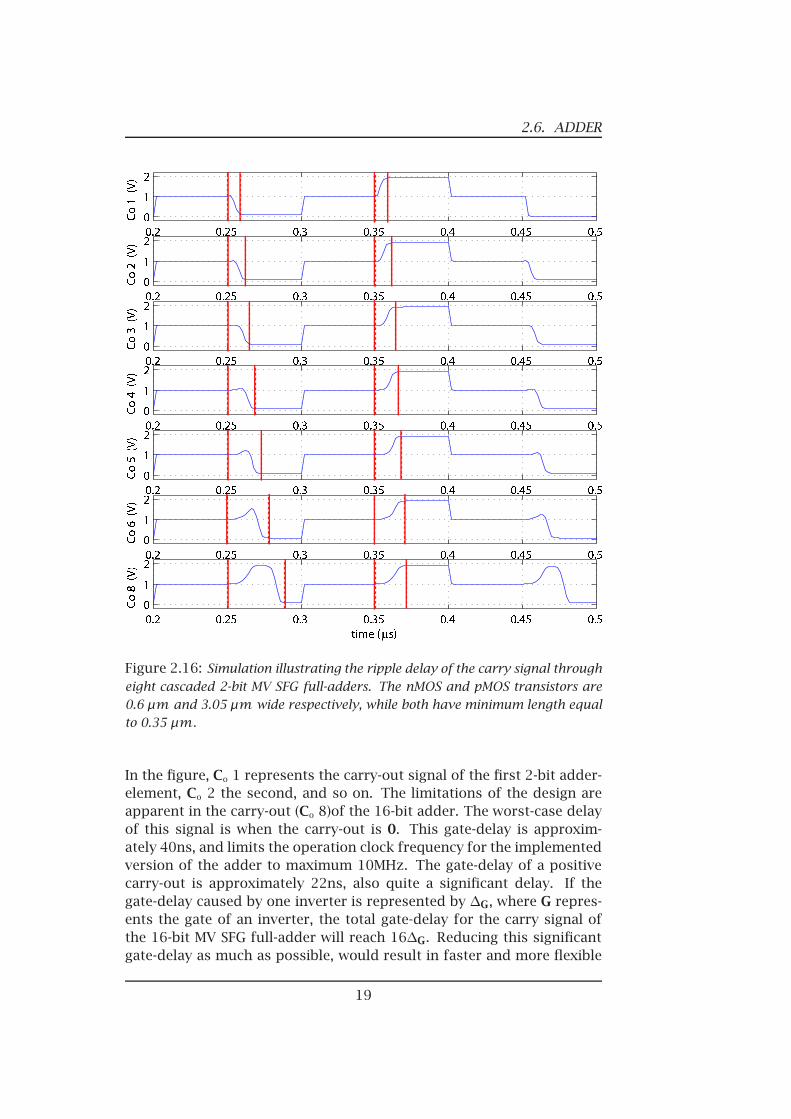
For each two-bit MV adder, the carry signal ripples through two inverters.This implies that a carry signal must ripple through sixteen inverters fora cascaded 16-bit MV full-adder. The result is a significant gate-delayaffecting the ripple of the carry signal. In Figure 2.16 the ripple delayof 16-bit MV full-adder is illustrated. The adders are stacked as shownin Figure 2.15. Also a a table providing the transistor sizes used, ispresented in Figure C.2.
17
2.6. ADDER
Figure 2.14: Single bit Binary Full-Adder.
Figure 2.15: The Figure illustrates the ripple of the carry signal when usingeight 2-bit SFG MV Adders cascaded, though only two adders are depicted here.
18
2.6. ADDER
Figure 2.16: Simulation illustrating the ripple delay of the carry signal througheight cascaded 2-bit MV SFG full-adders. The nMOS and pMOS transistors are0.6 µm and 3.05 µm wide respectively, while both have minimum length equalto 0.35 µm.
In the figure, Co 1 represents the carry-out signal of the first 2-bit adder-element, Co 2 the second, and so on. The limitations of the design areapparent in the carry-out (Co 8)of the 16-bit adder. The worst-case delayof this signal is when the carry-out is 0. This gate-delay is approxim-ately 40ns, and limits the operation clock frequency for the implementedversion of the adder to maximum 10MHz. The gate-delay of a positivecarry-out is approximately 22ns, also quite a significant delay. If thegate-delay caused by one inverter is represented by ∆G, where G repres-ents the gate of an inverter, the total gate-delay for the carry signal ofthe 16-bit MV SFG full-adder will reach 16∆G. Reducing this significantgate-delay as much as possible, would result in faster and more flexible
19
2.7. SUMMARY
adders.
Figure 2.16 also shows that the actual voltage change ∆V for the rechargeperiods happen in parallel, without any gate-delay. This implies that therecharge transistors do not impose any delay or limitations to the MVcircuits at this frequency. Therefore it is the carry rippling that imposesthe largest hindrance for the system.
2.7 Summary
In this chapter the basic multiple-value circuits, and the usage of thesehas been presented. The circuits described in this chapter can be usedin larger circuits, or adapted to give other beneficial solutions. Further-more the limitations of the presented MV adder has been pointed out.A possible solution to this problem would be to introduce a carry-look-ahead scheme, to decrease the delay on the carry signal. A MV carry-look-ahead full-adder is presented in the next chapter, along with a 16-bit carry-look-ahead scheme with a minimum delay regarding the carrysignal.
20
Chapter 3
The multiple-valued Carry LookAhead Adder
In this chapter a carry-look-ahead scheme for multiple-valuedlogics is proposed. Also, the prototype multiple-valued carry-look-ahead adder used in this scheme is presented and verifiedby measurements. The prototype adder makes use of the ba-sic components described in the previous chapter, but offersa much more effective carry-handling. Furthermore, the pro-posed carry-look-ahead scheme is explained using the proto-type chip and additional circuits.
The prototype adder designed for this thesis is a modified version of therecharge adder described in chapter two. For faster carry-handling, theprototype adder actually consists of two recharge adders and additionalgates. One of the adders calculates the correct Sum, while the otheradder, along with additional gates, is used for carry calculation. The factthat two MV adders and additional gates are used, more than doubles thesize of the adder compared to the recharge adder. On the other hand,the prototype adder offers a much more efficient carry-handling than therecharge adder, in terms of speed. By decreasing the gate-delay of thecarry signal, the adder can operate at faster frequencies. The decreaseof gate-delay also opens the opportunity to design adders that representmore than sixteen bits, while still using 2-bit adders as building blocks.
3.1 The Prototype Carry-Look-Ahead Full-Adder
For the prototype adder designed, the peripheral components describedin chapter two were used for the interface communicating with a binaryworld. This was done for two reasons. By surrounding the prototypeadder with the peripheral components, it would be possible to test if the
21
3.1. THE PROTOTYPE CARRY-LOOK-AHEAD FULL-ADDER
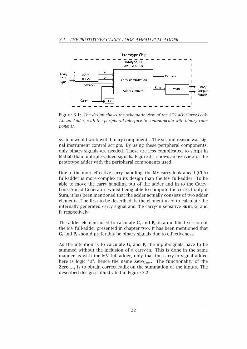
Figure 3.1: The design shows the schematic view of the SFG MV Carry-Look-Ahead Adder, with the peripheral interface to communicate with binary com-ponents.
system would work with binary components. The second reason was sig-nal instrument control scripts. By using these peripheral components,only binary signals are needed. These are less complicated to script inMatlab than multiple-valued signals. Figure 3.1 shows an overview of theprototype adder with the peripheral components used.
Due to the more effective carry-handling, the MV carry-look-ahead (CLA)full-adder is more complex in its design than the MV full-adder. To beable to move the carry-handling out of the adder and in to the Carry-Look-Ahead Generator, whilst being able to compute the correct outputSum, it has been mentioned that the adder actually consists of two adderelements. The first to be described, is the element used to calculate theinternally generated carry signal and the carry-in sensitive Sum, Gi andPi respectively.
The adder element used to calculate Gi and Pi, is a modified version ofthe MV full-adder presented in chapter two. It has been mentioned thatGi and Pi should preferably be binary signals due to effectiveness.
As the intention is to calculate Gi and Pi the input-signals have to besummed without the inclusion of a carry-in. This is done in the samemanner as with the MV full-adder, only that the carry-in signal addedhere is logic “0”, hence the name ZeroCarry. The functionality of theZeroCarry is to obtain correct radix on the summation of the inputs. Thedescribed design is illustrated in Figure 3.2.
22
3.1. THE PROTOTYPE CARRY-LOOK-AHEAD FULL-ADDER
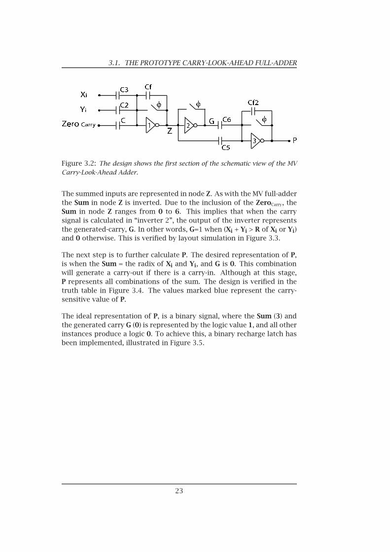
Figure 3.2: The design shows the first section of the schematic view of the MVCarry-Look-Ahead Adder.
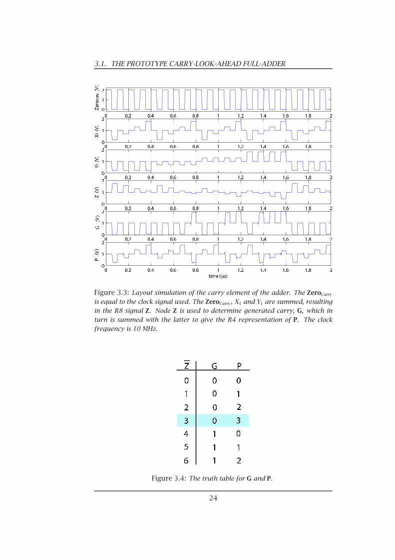
The summed inputs are represented in node Z. As with the MV full-adderthe Sum in node Z is inverted. Due to the inclusion of the ZeroCarry, theSum in node Z ranges from 0 to 6. This implies that when the carrysignal is calculated in “inverter 2”, the output of the inverter representsthe generated-carry, G. In other words, G=1 when (Xi + Yi > R of Xi or Yi)and 0 otherwise. This is verified by layout simulation in Figure 3.3.
The next step is to further calculate P. The desired representation of P,is when the Sum = the radix of Xi and Yi, and G is 0. This combinationwill generate a carry-out if there is a carry-in. Although at this stage,P represents all combinations of the sum. The design is verified in thetruth table in Figure 3.4. The values marked blue represent the carry-sensitive value of P.
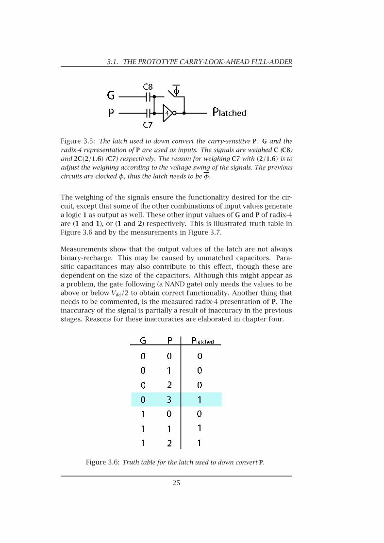
The ideal representation of P, is a binary signal, where the Sum (3) andthe generated carry G (0) is represented by the logic value 1, and all otherinstances produce a logic 0. To achieve this, a binary recharge latch hasbeen implemented, illustrated in Figure 3.5.
23
3.1. THE PROTOTYPE CARRY-LOOK-AHEAD FULL-ADDER
Figure 3.3: Layout simulation of the carry element of the adder. The ZeroCarry
is equal to the clock signal used. The ZeroCarry, Xi and Yi are summed, resultingin the R8 signal Z. Node Z is used to determine generated carry, G, which inturn is summed with the latter to give the R4 representation of P. The clockfrequency is 10 MHz.
Figure 3.4: The truth table for G and P.
24
3.1. THE PROTOTYPE CARRY-LOOK-AHEAD FULL-ADDER
Figure 3.5: The latch used to down convert the carry-sensitive P. G and theradix-4 representation of P are used as inputs. The signals are weighed C (C8)and 2C(2/1.6) (C7) respectively. The reason for weighing C7 with (2/1.6) is toadjust the weighing according to the voltage swing of the signals. The previouscircuits are clocked φ, thus the latch needs to be φ.
The weighing of the signals ensure the functionality desired for the cir-cuit, except that some of the other combinations of input values generatea logic 1 as output as well. These other input values of G and P of radix-4are (1 and 1), or (1 and 2) respectively. This is illustrated truth table inFigure 3.6 and by the measurements in Figure 3.7.
Measurements show that the output values of the latch are not alwaysbinary-recharge. This may be caused by unmatched capacitors. Para-sitic capacitances may also contribute to this effect, though these aredependent on the size of the capacitors. Although this might appear asa problem, the gate following (a NAND gate) only needs the values to beabove or below Vdd/2 to obtain correct functionality. Another thing thatneeds to be commented, is the measured radix-4 presentation of P. Theinaccuracy of the signal is partially a result of inaccuracy in the previousstages. Reasons for these inaccuracies are elaborated in chapter four.
Figure 3.6: Truth table for the latch used to down convert P.
25
3.1. THE PROTOTYPE CARRY-LOOK-AHEAD FULL-ADDER
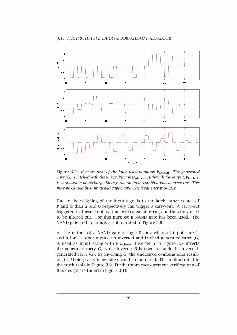
Figure 3.7: Measurement of the latch used to obtain Platched. The generatedcarry G, is latched with the P, resulting in Platched. Although the output, Platched,is supposed to be recharge-binary, not all input combinations achieve this. Thismay be caused by unmatched capacitors. The frequency is 500Hz.
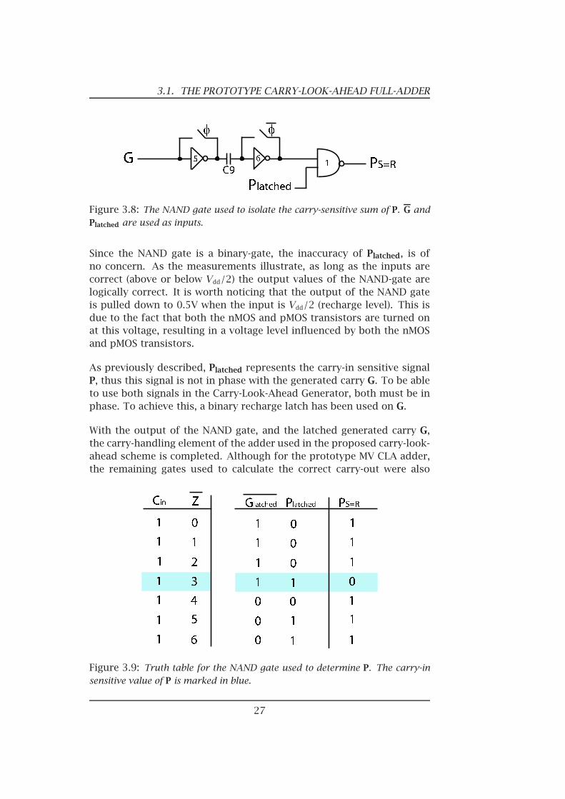
Due to the weighing of the input signals to the latch, other values ofP and G than 3 and 0 respectively can trigger a carry-out. A carry-outtriggered by these combinations will cause bit error, and thus they needto be filtered out. For this purpose a NAND gate has been used. TheNAND gate and its inputs are illustrated in Figure 3.8.
As the output of a NAND gate is logic 0 only when all inputs are 1,and 0 for all other inputs, an inverted and latched generated-carry (G)is used as input along with Platched. Inverter 5 in Figure 3.8 invertsthe generated-carry G, while inverter 6 is used to latch the inverted-generated-carry (G). By inverting G, the undesired combinations result-ing in P being carry-in sensitive can be eliminated. This is illustrated inthe truth table in Figure 3.9. Furthermore measurement verifications ofthis design are found in Figure 3.10.
26
3.1. THE PROTOTYPE CARRY-LOOK-AHEAD FULL-ADDER
Figure 3.8: The NAND gate used to isolate the carry-sensitive sum of P. G andPlatched are used as inputs.
Since the NAND gate is a binary-gate, the inaccuracy of Platched, is ofno concern. As the measurements illustrate, as long as the inputs arecorrect (above or below Vdd/2) the output values of the NAND-gate arelogically correct. It is worth noticing that the output of the NAND gateis pulled down to 0.5V when the input is Vdd/2 (recharge level). This isdue to the fact that both the nMOS and pMOS transistors are turned onat this voltage, resulting in a voltage level influenced by both the nMOSand pMOS transistors.
As previously described, Platched represents the carry-in sensitive signalP, thus this signal is not in phase with the generated carry G. To be ableto use both signals in the Carry-Look-Ahead Generator, both must be inphase. To achieve this, a binary recharge latch has been used on G.
With the output of the NAND gate, and the latched generated carry G,the carry-handling element of the adder used in the proposed carry-look-ahead scheme is completed. Although for the prototype MV CLA adder,the remaining gates used to calculate the correct carry-out were also
Figure 3.9: Truth table for the NAND gate used to determine P. The carry-insensitive value of P is marked in blue.
27

3.1. THE PROTOTYPE CARRY-LOOK-AHEAD FULL-ADDER
Figure 3.10: Measurement of the NAND gate used to isolate the carry-sensitivesum of P. G and Platched are used as inputs. The frequency is 500Hz.
included. The reason for including the remaining gates, was to verifythe design by measurements.
The gates of the Carry-Look-Ahead Generator included in the prototypeMV CLA adder are two NOR gates and a binary inverter. As the carry-inneeds to be included, whilst the generated carry must be added to theeventual propagating carry, NOR gates have been found to be ideal. Thedesired function of the gate summing P and the carry-in, is that only thepropagating carry is represented by a logic 1 as output, as this outputis added to the generated carry. To achieve a logic 1 for the desiredvalues only, the carry-in needs to be inverted, as both the carry-sensitivevalue of P and the carry-in will be represented by a logic 0. For thispurpose a binary inverter is used. This inverter can seem redundant,since an inverted carry-in signal could have been used. The reason forchoosing a positive carry-in and inverting it is explained in the sectionpresenting the proposed CLA scheme. Figure 3.11 illustrates the NORgates included in the prototype MV CLA adder as well as the inverterused to invert the carry-in signal.
28
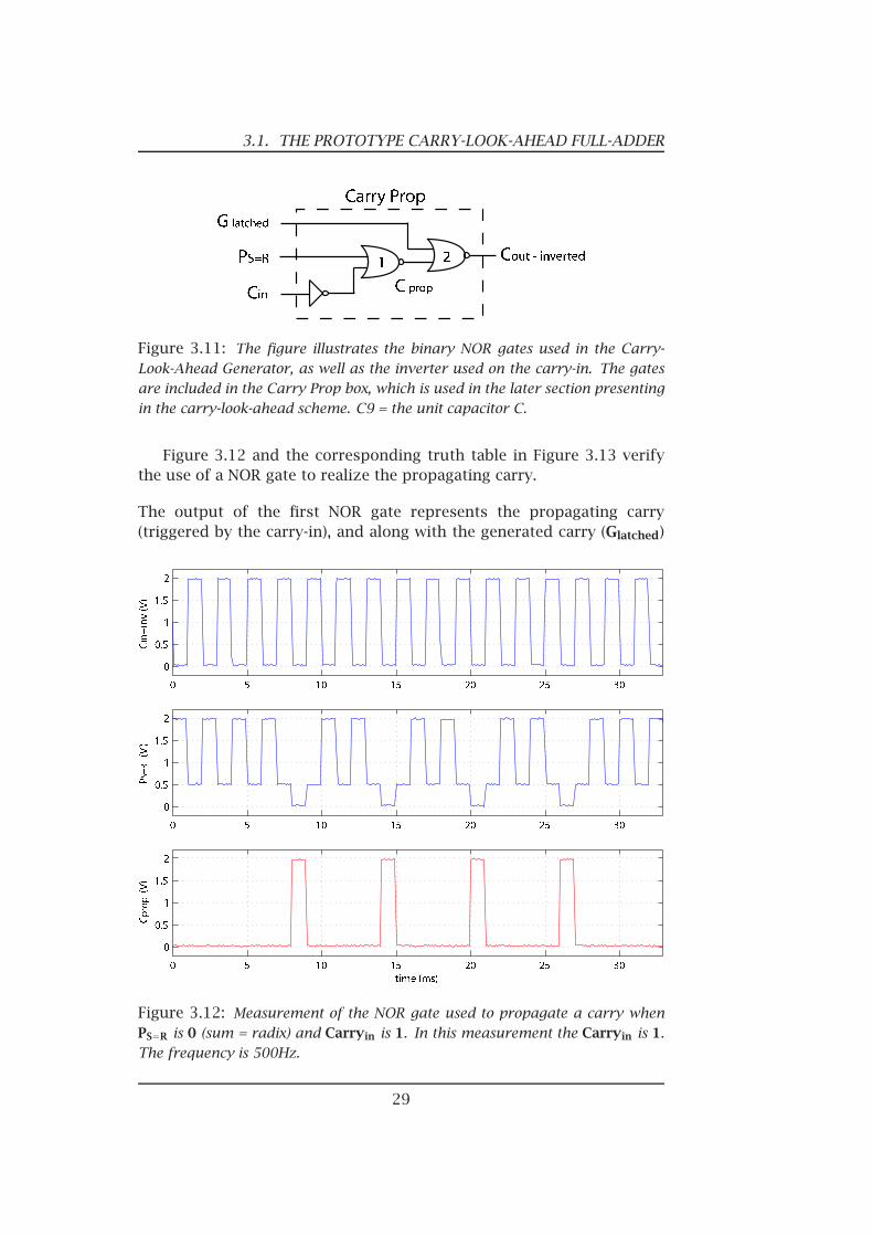
3.1. THE PROTOTYPE CARRY-LOOK-AHEAD FULL-ADDER
Figure 3.11: The figure illustrates the binary NOR gates used in the Carry-Look-Ahead Generator, as well as the inverter used on the carry-in. The gatesare included in the Carry Prop box, which is used in the later section presentingin the carry-look-ahead scheme. C9 = the unit capacitor C.
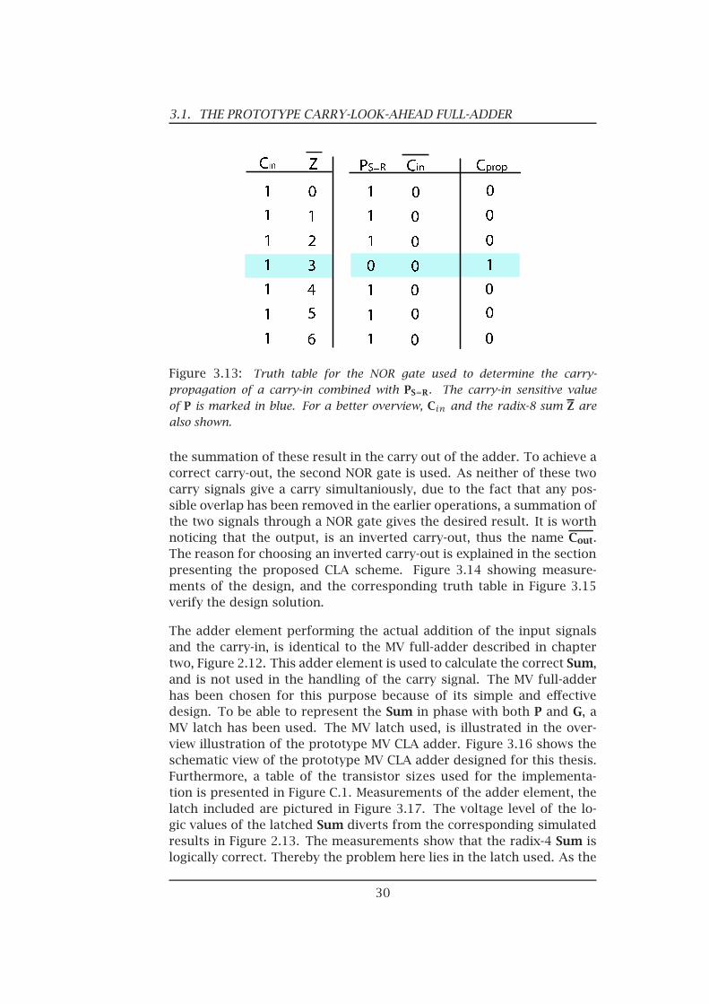
Figure 3.12 and the corresponding truth table in Figure 3.13 verifythe use of a NOR gate to realize the propagating carry.
The output of the first NOR gate represents the propagating carry(triggered by the carry-in), and along with the generated carry (Glatched)
Figure 3.12: Measurement of the NOR gate used to propagate a carry whenPS=R is 0 (sum = radix) and Carryin is 1. In this measurement the Carryin is 1.The frequency is 500Hz.
29
3.1. THE PROTOTYPE CARRY-LOOK-AHEAD FULL-ADDER
Figure 3.13: Truth table for the NOR gate used to determine the carry-propagation of a carry-in combined with PS=R. The carry-in sensitive valueof P is marked in blue. For a better overview, Cin and the radix-8 sum Z arealso shown.
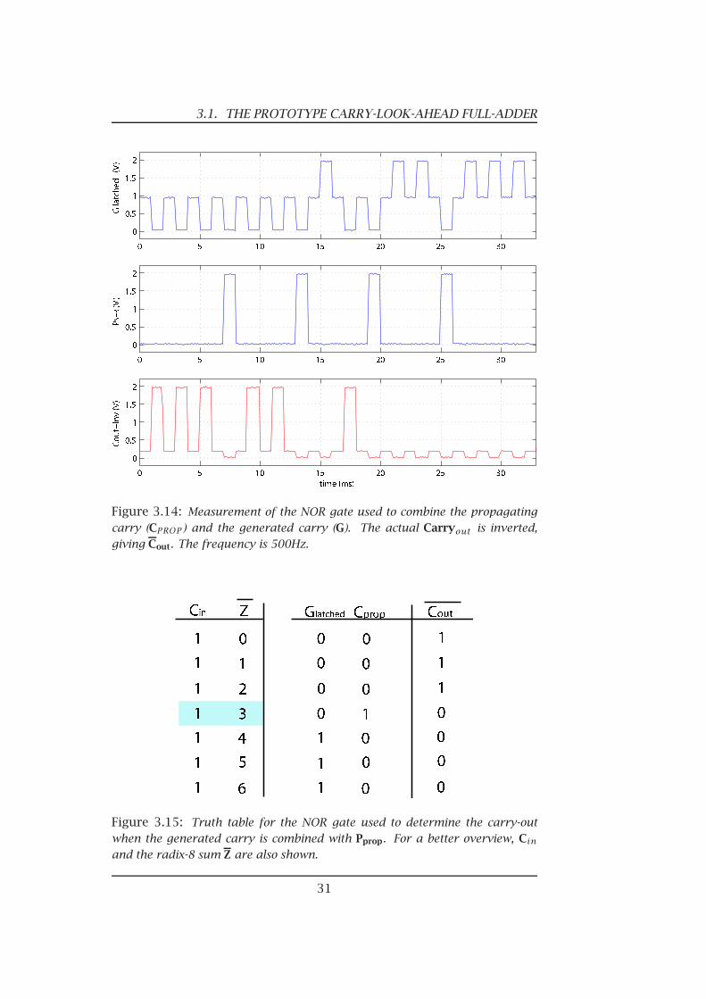
the summation of these result in the carry out of the adder. To achieve acorrect carry-out, the second NOR gate is used. As neither of these twocarry signals give a carry simultaniously, due to the fact that any pos-sible overlap has been removed in the earlier operations, a summation ofthe two signals through a NOR gate gives the desired result. It is worthnoticing that the output, is an inverted carry-out, thus the name Cout.The reason for choosing an inverted carry-out is explained in the sectionpresenting the proposed CLA scheme. Figure 3.14 showing measure-ments of the design, and the corresponding truth table in Figure 3.15verify the design solution.
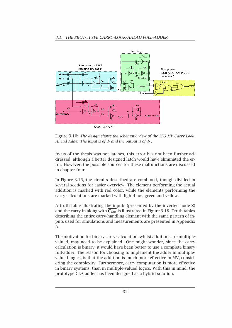
The adder element performing the actual addition of the input signalsand the carry-in, is identical to the MV full-adder described in chaptertwo, Figure 2.12. This adder element is used to calculate the correct Sum,and is not used in the handling of the carry signal. The MV full-adderhas been chosen for this purpose because of its simple and effectivedesign. To be able to represent the Sum in phase with both P and G, aMV latch has been used. The MV latch used, is illustrated in the over-view illustration of the prototype MV CLA adder. Figure 3.16 shows theschematic view of the prototype MV CLA adder designed for this thesis.Furthermore, a table of the transistor sizes used for the implementa-tion is presented in Figure C.1. Measurements of the adder element, thelatch included are pictured in Figure 3.17. The voltage level of the lo-gic values of the latched Sum diverts from the corresponding simulatedresults in Figure 2.13. The measurements show that the radix-4 Sum islogically correct. Thereby the problem here lies in the latch used. As the
30
3.1. THE PROTOTYPE CARRY-LOOK-AHEAD FULL-ADDER
Figure 3.14: Measurement of the NOR gate used to combine the propagatingcarry (CPROP ) and the generated carry (G). The actual Carryout is inverted,giving Cout. The frequency is 500Hz.
Figure 3.15: Truth table for the NOR gate used to determine the carry-outwhen the generated carry is combined with Pprop. For a better overview, Cinand the radix-8 sum Z are also shown.
31
3.1. THE PROTOTYPE CARRY-LOOK-AHEAD FULL-ADDER
Figure 3.16: The design shows the schematic view of the SFG MV Carry-Look-Ahead Adder The input is of φ and the output is of φ .
focus of the thesis was not latches, this error has not been further ad-dressed, although a better designed latch would have eliminated the er-ror. However, the possible sources for these malfunctions are discussedin chapter four.
In Figure 3.16, the circuits described are combined, though divided inseveral sections for easier overview. The element performing the actualaddition is marked with red color, while the elements performing thecarry calculations are marked with light-blue, green and yellow.
A truth table illustrating the inputs (presented by the inverted node Z)and the carry-in along with COut is illustrated in Figure 3.18. Truth tablesdescribing the entire carry-handling element with the same pattern of in-puts used for simulations and measurements are presented in AppendixA.
The motivation for binary carry calculation, whilst additions are multiple-valued, may need to be explained. One might wonder, since the carrycalculation is binary, it would have been better to use a complete binaryfull-adder. The reason for choosing to implement the adder in multiple-valued logics, is that the addition is much more effective in MV, consid-ering the complexity. Furthermore, carry computation is more effectivein binary systems, than in multiple-valued logics. With this in mind, theprototype CLA adder has been designed as a hybrid solution.
32
3.2. PROTOTYPE ADDER USED IN CASCADE
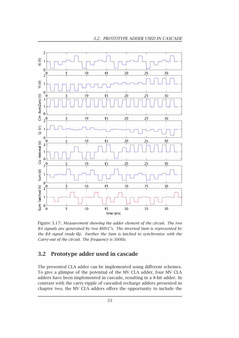
Figure 3.17: Measurement showing the adder element of the circuit. The twoR4 signals are generated by two BMVC’s. The inverted Sum is represented bythe R8 signal (node Q). Further the Sum is latched to synchronize with theCarry-out of the circuit. The frequency is 500Hz.
3.2 Prototype adder used in cascade
The presented CLA adder can be implemented using different schemes.To give a glimpse of the potential of the MV CLA adder, four MV CLAadders have been implemented in cascade, resulting in a 8-bit adder. Incontrast with the carry-ripple of cascaded recharge adders presented inchapter two, the MV CLA adders offers the opportunity to include the
33
3.2. PROTOTYPE ADDER USED IN CASCADE
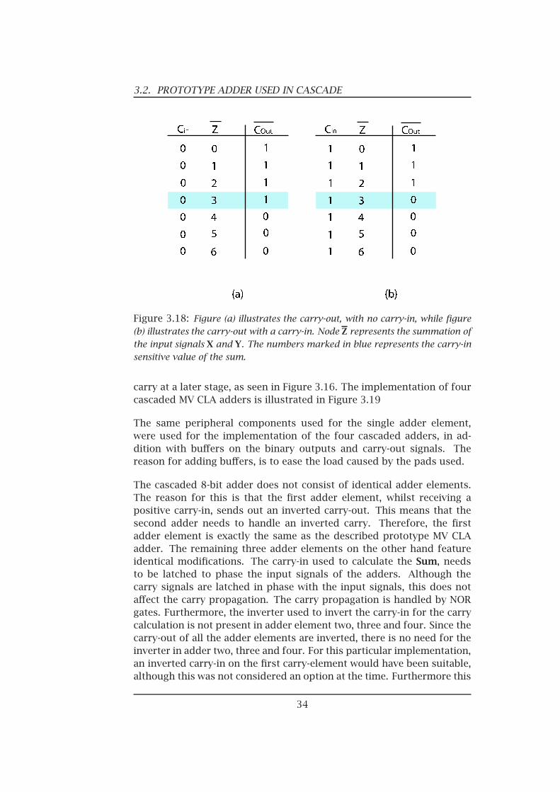
Figure 3.18: Figure (a) illustrates the carry-out, with no carry-in, while figure(b) illustrates the carry-out with a carry-in. Node Z represents the summation ofthe input signals X and Y. The numbers marked in blue represents the carry-insensitive value of the sum.
carry at a later stage, as seen in Figure 3.16. The implementation of fourcascaded MV CLA adders is illustrated in Figure 3.19
The same peripheral components used for the single adder element,were used for the implementation of the four cascaded adders, in ad-dition with buffers on the binary outputs and carry-out signals. Thereason for adding buffers, is to ease the load caused by the pads used.
The cascaded 8-bit adder does not consist of identical adder elements.The reason for this is that the first adder element, whilst receiving apositive carry-in, sends out an inverted carry-out. This means that thesecond adder needs to handle an inverted carry. Therefore, the firstadder element is exactly the same as the described prototype MV CLAadder. The remaining three adder elements on the other hand featureidentical modifications. The carry-in used to calculate the Sum, needsto be latched to phase the input signals of the adders. Although thecarry signals are latched in phase with the input signals, this does notaffect the carry propagation. The carry propagation is handled by NORgates. Furthermore, the inverter used to invert the carry-in for the carrycalculation is not present in adder element two, three and four. Since thecarry-out of all the adder elements are inverted, there is no need for theinverter in adder two, three and four. For this particular implementation,an inverted carry-in on the first carry-element would have been suitable,although this was not considered an option at the time. Furthermore this
34

3.2. PROTOTYPE ADDER USED IN CASCADE
Figure 3.19: The prototype MV CLA adder used in cascade.
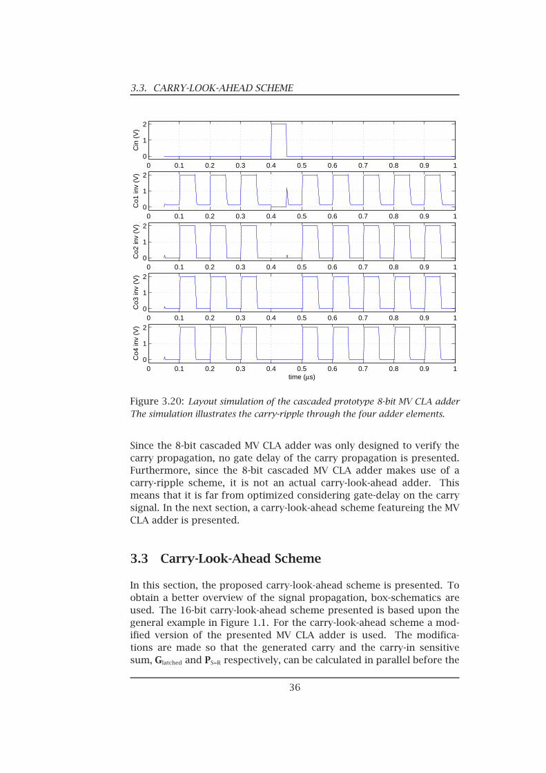
eight bit implementation was only designed to see that the carry signalsripple was correct from adder to adder. A simulation of the carry-rippleis illustrated in Figure 3.20.
As the carry-out is inverted, a logic 0 represents a carry propagation.The recharge signals from the MV calculations are also represented bylogic 0. The recharge-level of logic 0 has no effect on the calculation ofthe carry to the next element, as seen in the simulation. The simulationshows that a carry-in does not result in a shift of the signal. The shiftcomes if there is no carry-out, as the carry signal is low by default dueto the recharge levels.
35
3.3. CARRY-LOOK-AHEAD SCHEME
0 0.1 0.2 0.3 0.4 0.5 0.6 0.7 0.8 0.9 10
1
2
Cin
(V
)
0 0.1 0.2 0.3 0.4 0.5 0.6 0.7 0.8 0.9 10
1
2
Co1
inv
(V)
0 0.1 0.2 0.3 0.4 0.5 0.6 0.7 0.8 0.9 10
1
2
Co2
inv
(V)
0 0.1 0.2 0.3 0.4 0.5 0.6 0.7 0.8 0.9 10
1
2
Co3
inv
(V)
0 0.1 0.2 0.3 0.4 0.5 0.6 0.7 0.8 0.9 10
1
2
Co4
inv
(V)
time (µs)
Figure 3.20: Layout simulation of the cascaded prototype 8-bit MV CLA adderThe simulation illustrates the carry-ripple through the four adder elements.
Since the 8-bit cascaded MV CLA adder was only designed to verify thecarry propagation, no gate delay of the carry propagation is presented.Furthermore, since the 8-bit cascaded MV CLA adder makes use of acarry-ripple scheme, it is not an actual carry-look-ahead adder. Thismeans that it is far from optimized considering gate-delay on the carrysignal. In the next section, a carry-look-ahead scheme featureing the MVCLA adder is presented.
3.3 Carry-Look-Ahead Scheme
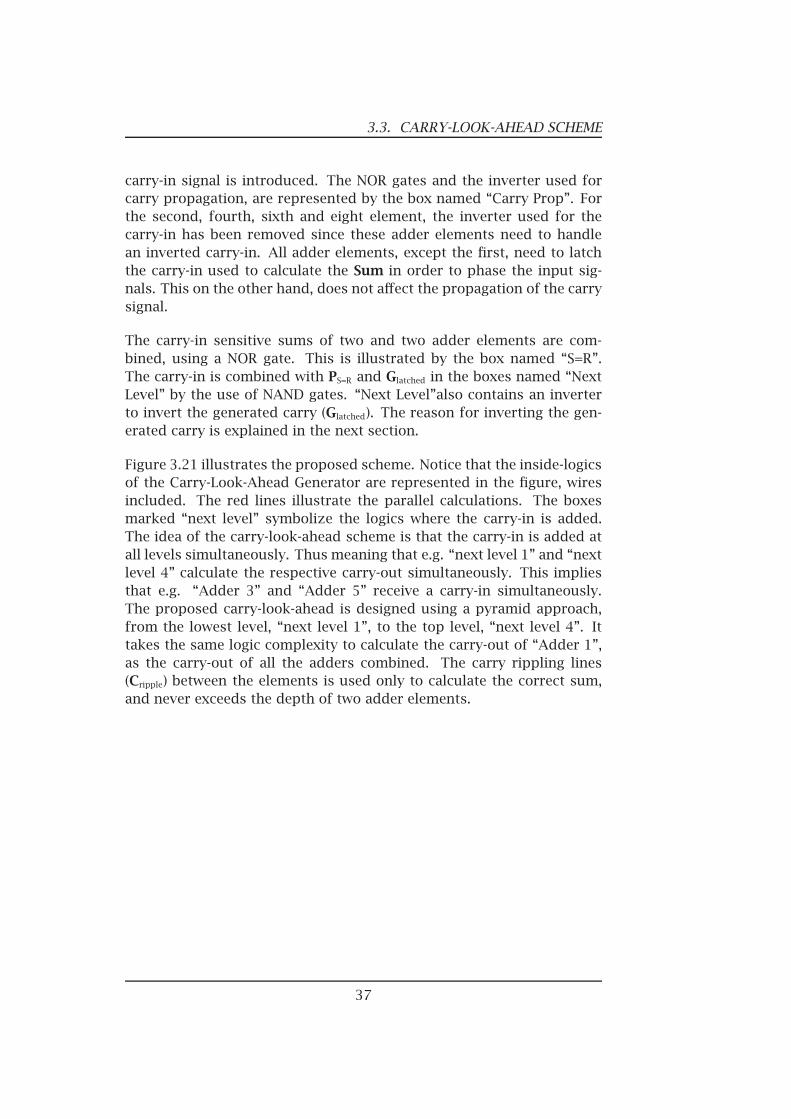
In this section, the proposed carry-look-ahead scheme is presented. Toobtain a better overview of the signal propagation, box-schematics areused. The 16-bit carry-look-ahead scheme presented is based upon thegeneral example in Figure 1.1. For the carry-look-ahead scheme a mod-ified version of the presented MV CLA adder is used. The modifica-tions are made so that the generated carry and the carry-in sensitivesum, Glatched and PS=R respectively, can be calculated in parallel before the
36
3.3. CARRY-LOOK-AHEAD SCHEME
carry-in signal is introduced. The NOR gates and the inverter used forcarry propagation, are represented by the box named “Carry Prop”. Forthe second, fourth, sixth and eight element, the inverter used for thecarry-in has been removed since these adder elements need to handlean inverted carry-in. All adder elements, except the first, need to latchthe carry-in used to calculate the Sum in order to phase the input sig-nals. This on the other hand, does not affect the propagation of the carrysignal.
The carry-in sensitive sums of two and two adder elements are com-bined, using a NOR gate. This is illustrated by the box named “S=R”.The carry-in is combined with PS=R and Glatched in the boxes named “NextLevel” by the use of NAND gates. “Next Level”also contains an inverterto invert the generated carry (Glatched). The reason for inverting the gen-erated carry is explained in the next section.
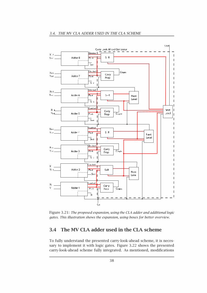
Figure 3.21 illustrates the proposed scheme. Notice that the inside-logicsof the Carry-Look-Ahead Generator are represented in the figure, wiresincluded. The red lines illustrate the parallel calculations. The boxesmarked “next level” symbolize the logics where the carry-in is added.The idea of the carry-look-ahead scheme is that the carry-in is added atall levels simultaneously. Thus meaning that e.g. “next level 1” and “nextlevel 4” calculate the respective carry-out simultaneously. This impliesthat e.g. “Adder 3” and “Adder 5” receive a carry-in simultaneously.The proposed carry-look-ahead is designed using a pyramid approach,from the lowest level, “next level 1”, to the top level, “next level 4”. Ittakes the same logic complexity to calculate the carry-out of “Adder 1”,as the carry-out of all the adders combined. The carry rippling lines(Cripple) between the elements is used only to calculate the correct sum,and never exceeds the depth of two adder elements.
37
3.4. THE MV CLA ADDER USED IN THE CLA SCHEME
Figure 3.21: The proposed expansion, using the CLA adder and additional logicgates. This illustration shows the expansion, using boxes for better overview.
3.4 The MV CLA adder used in the CLA scheme
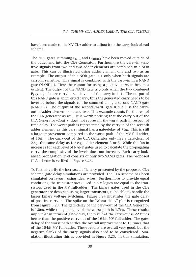
To fully understand the presented carry-look-ahead scheme, it is neces-sary to implement it with logic gates. Figure 3.22 shows the presentedcarry-look-ahead scheme fully integrated. As mentioned, modifications
38
3.4. THE MV CLA ADDER USED IN THE CLA SCHEME
have been made to the MV CLA adder to adjust it to the carry-look-aheadscheme.
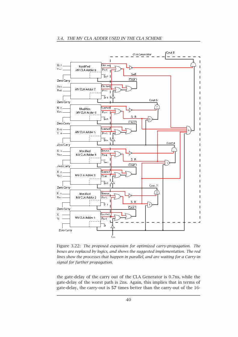
The NOR gates summing PS=R and Glatched have been moved outside ofthe adder and into the CLA Generator. Furthermore the carry-in sens-itive signals from two and two adder elements are combined in a NORgate. This can be illustrated using adder element one and two as anexample. The output of this NOR gate is 1 only when both signals arecarry-in sensitive. This signal is combined with the carry-in in a NANDgate (NAND 1). Here the reason for using a positive carry-in becomesevident. The output of the NAND gate is 0 only when the two combinedPS=R signals are carry-in sensitive and the carry-in is 1. The output ofthis NAND gate is an inverted carry, thus the generated carry needs to beinverted before the signals can be summed using a second NAND gate(NAND 2). The output of the second NAND gate (Cout 2) is the carry-out of adder elements one and two. This example counts for the rest ofthe CLA generator as well. It is worth noticing that the carry-out of theCLA Generator (Cout 8) does not represent the worst path in respect oftime-delay. The worst path is represented by the carry-in of the seventhadder element, as this carry signal has a gate-delay of 7∆G. This is stilla large improvement compared to the worst path of the MV full-adder,of 16∆G. The carry-out of the CLA Generator only has a gate-delay of2∆G, the same delay as for e.g. adder element 3 or 5. While the fan-inincreases for each level of NAND gates used to calculate the propagatingcarry, the complexity of the levels does not increase. Each carry-look-ahead propagation level consists of only two NAND gates. The proposedCLA scheme is verified in Figure 3.23.
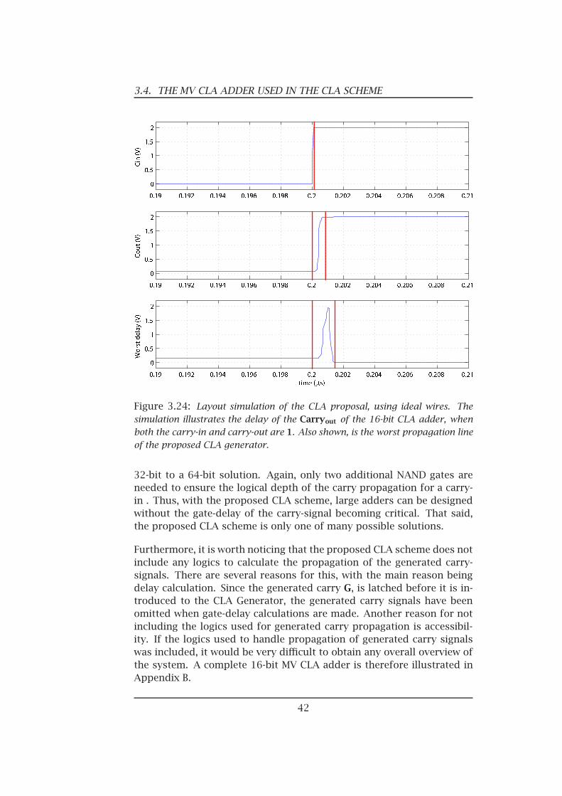
To further verify the increased efficiency presented by the proposed CLAscheme, gate-delay simulations are provided. The CLA scheme has beensimulated on layout, using ideal wires. Furthermore to provide equalconditions, the transistor sizes used in MV logics are equal to the tran-sistors used in the MV full-adder. The binary gates used in the CLAgenerator are designed using larger transistors, to be able to handle thelarger binary voltage switching. Figure 3.24 illustrates the gate delayof positive carry-in. The spike on the “Worst delay” plot is recognizedfrom Figure 3.23. The gate-delay of the carry-out of the CLA Generatoris 1.0ns, while the gate-delay of the worst path is 1.7ns. These resultsimply that in terms of gate-delay, the result of the carry-out is 22 timesbetter than the positive carry-out of the 16-bit MV full-adder. The gate-delay of the worst path settles the overall improvement to 13 times thatof the 16-bit MV full-adder. These results are overall very good, but thenegative flanks of the carry signals also need to be considered. Sim-ulation illustrating this is provided in Figure 3.25. In this simulation,
39
3.4. THE MV CLA ADDER USED IN THE CLA SCHEME
Figure 3.22: The proposed expansion for optimized carry-propagation. Theboxes are replaced by logics, and shows the suggested implementation. The redlines show the processes that happen in parallel, and are waiting for a Carry-insignal for further propagation.
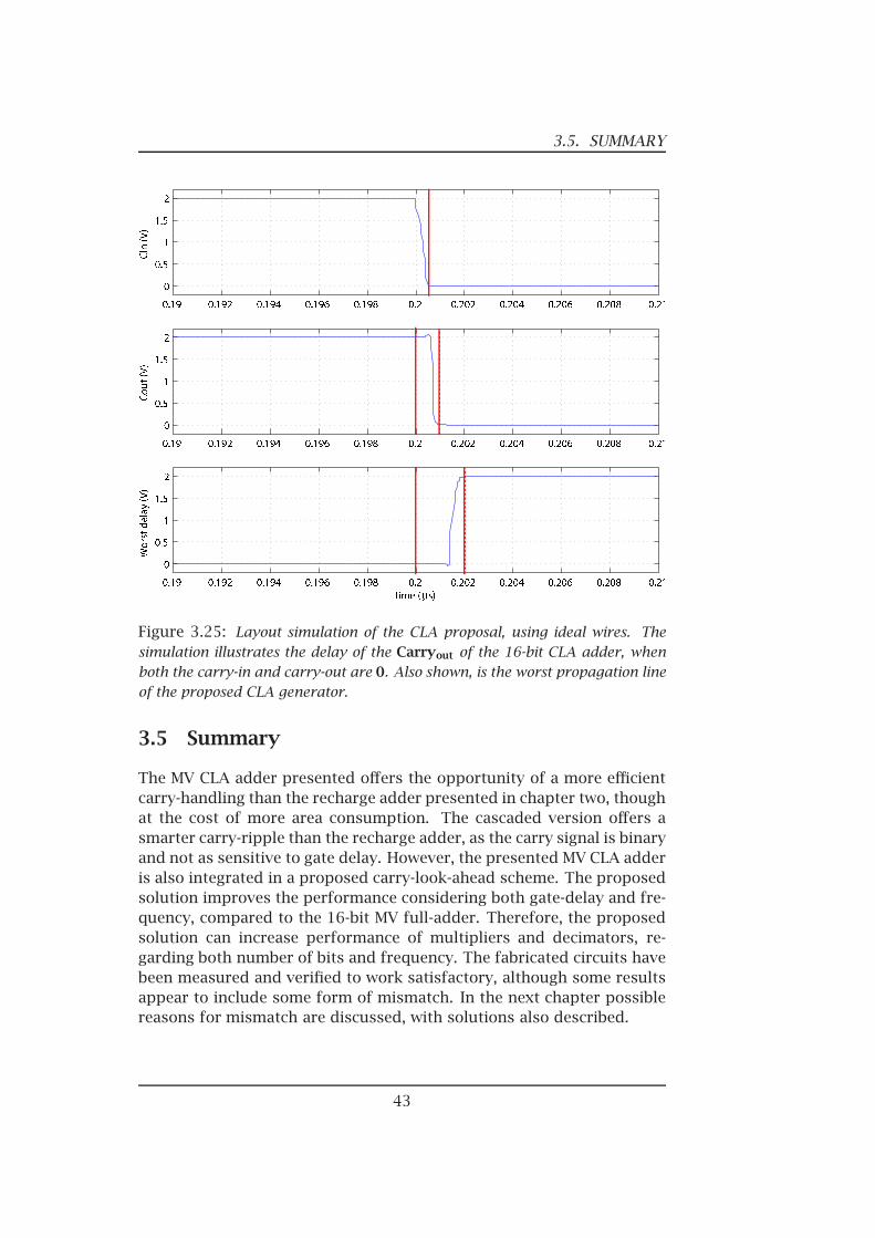
the gate-delay of the carry out of the CLA Generator is 0.7ns, while thegate-delay of the worst path is 2ns. Again, this implies that in terms ofgate-delay, the carry-out is 57 times better than the carry-out of the 16-
40
3.4. THE MV CLA ADDER USED IN THE CLA SCHEME
0.1 0.15 0.2 0.25 0.3 0.35 0.4 0.45 0.50
1
2
Cin
(V
)
0.1 0.15 0.2 0.25 0.3 0.35 0.4 0.45 0.50
1
2
Cou
t2 (
V)
0.1 0.15 0.2 0.25 0.3 0.35 0.4 0.45 0.50
1
2
Cou
t4 (
V)
0.1 0.15 0.2 0.25 0.3 0.35 0.4 0.45 0.50
1
2
Cou
t8 (
V)
0.1 0.15 0.2 0.25 0.3 0.35 0.4 0.45 0.50
1
2
Cou
t7 in
v (V
)
time (µs)
Figure 3.23: Layout simulation of the CLA proposal, using ideal wires. Thesimulation illsustrates the scenario where G = 0, P = 0 (Sum = radix) and Carryin
= 1. The frequency is 10MHz.
bit MV full-adder. The worst path gate-delays for both adders are 40nsand 2ns for the 16-bit MV full-adder and the 16-bit MV CLA full-adder re-spectively. This implies that by using the proposed CLA scheme, an im-provement of a factor twenty is achieved considering a carry-in triggeredripple. Furthermore, the worst delay of 2ns implies that the implemen-ted CLA Generator can operate at frequencies up to 500MHz. Since theadder elements used are not affected by the gate-delay of the ripplingcarry signal, these too can operate at higher frequency than the adderelements of the 16-bit MV full-adder. The MV CLA adder has been simu-lated to operate logically correct at a frequency of 50MHz, illustrated inchapter four. This gives an overall frequency improvement of a factor 5,when compared to the 16-bit MV full-adder.
The improvement in gate-delay also opens the opportunity to designlarger adders. It is possible to expand the 16-bit MV CLA adder to a32-bit MV CLA adder with only two additional NAND gates to handlethe computation of a carry-in. The same counts for an expansion from
41
3.4. THE MV CLA ADDER USED IN THE CLA SCHEME
Figure 3.24: Layout simulation of the CLA proposal, using ideal wires. Thesimulation illustrates the delay of the Carryout of the 16-bit CLA adder, whenboth the carry-in and carry-out are 1. Also shown, is the worst propagation lineof the proposed CLA generator.
32-bit to a 64-bit solution. Again, only two additional NAND gates areneeded to ensure the logical depth of the carry propagation for a carry-in . Thus, with the proposed CLA scheme, large adders can be designedwithout the gate-delay of the carry-signal becoming critical. That said,the proposed CLA scheme is only one of many possible solutions.
Furthermore, it is worth noticing that the proposed CLA scheme does notinclude any logics to calculate the propagation of the generated carry-signals. There are several reasons for this, with the main reason beingdelay calculation. Since the generated carry G, is latched before it is in-troduced to the CLA Generator, the generated carry signals have beenomitted when gate-delay calculations are made. Another reason for notincluding the logics used for generated carry propagation is accessibil-ity. If the logics used to handle propagation of generated carry signalswas included, it would be very difficult to obtain any overall overview ofthe system. A complete 16-bit MV CLA adder is therefore illustrated inAppendix B.
42
3.5. SUMMARY
Figure 3.25: Layout simulation of the CLA proposal, using ideal wires. Thesimulation illustrates the delay of the Carryout of the 16-bit CLA adder, whenboth the carry-in and carry-out are 0. Also shown, is the worst propagation lineof the proposed CLA generator.
3.5 Summary
The MV CLA adder presented offers the opportunity of a more efficientcarry-handling than the recharge adder presented in chapter two, thoughat the cost of more area consumption. The cascaded version offers asmarter carry-ripple than the recharge adder, as the carry signal is binaryand not as sensitive to gate delay. However, the presented MV CLA adderis also integrated in a proposed carry-look-ahead scheme. The proposedsolution improves the performance considering both gate-delay and fre-quency, compared to the 16-bit MV full-adder. Therefore, the proposedsolution can increase performance of multipliers and decimators, re-garding both number of bits and frequency. The fabricated circuits havebeen measured and verified to work satisfactory, although some resultsappear to include some form of mismatch. In the next chapter possiblereasons for mismatch are discussed, with solutions also described.
43

3.5. SUMMARY
44
Chapter 4
System Considerations
Although the presented circuits work perfectly in theory, andalso when simulated in layout, mismatch in the componentscan alter the functionality of the system. In this chapter pos-sible sources for malfunction are discussed, with possible solu-tions also presented. Furthermore power consumption andmax frequency of the MV CLA adder are discussed. The layoutof the prototype design is also described, providing argument-ation for the design methods used.
4.1 Sources of malfunction
When implementing multiple-valued designs, as with any other designtechnique, there are always elements that can cause malfunction. Po-tential sources of malfunction are discussed in this section. To obtainthe most linear representation of the MV signals, the operation range ofthe signals has been set between 0.2v - 1.8V. The reason for this is thatthe gain decreases near Vdd and Vss, since the transistors enter the lin-ear region. Although helpful, this precaution is not enough to preventmismatch as other factors contribute as well.
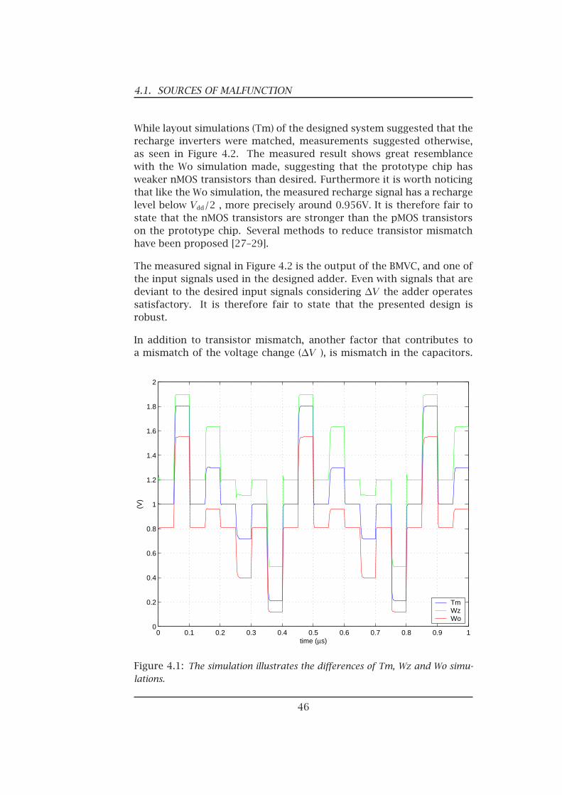
First the problem of mismatch between the transistors is considered.A mismatch between the nMOS and pMOS transistor in a recharge in-verter, will result in a recharge level different of Vdd/2 . Furthermore,a mismatch between the recharge transistors, will contribute to a mis-match to the voltage swing (∆V ) of the logic levels. Figure 4.1 shows asimulation of the worst possible scenario on a single chip, consideringnMOS and pMOS matching. The worst-one (Wo, weak pMOS in Cadence)simulation and the worst-zero (Wz, weak nMOS in Cadence) simulationsare compared to the typical mean (Tm) simulation.
45
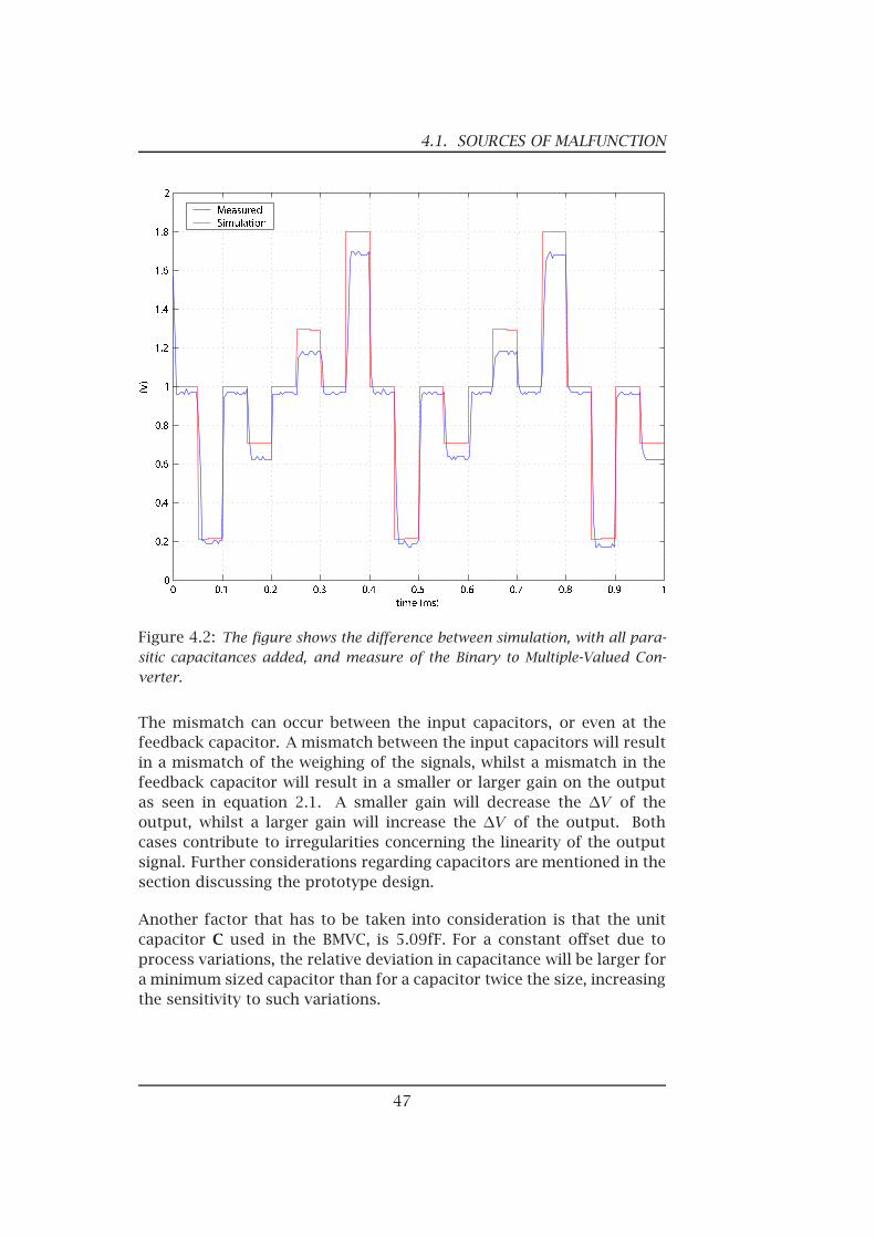
4.1. SOURCES OF MALFUNCTION
While layout simulations (Tm) of the designed system suggested that therecharge inverters were matched, measurements suggested otherwise,as seen in Figure 4.2. The measured result shows great resemblancewith the Wo simulation made, suggesting that the prototype chip hasweaker nMOS transistors than desired. Furthermore it is worth noticingthat like the Wo simulation, the measured recharge signal has a rechargelevel below Vdd/2 , more precisely around 0.956V. It is therefore fair tostate that the nMOS transistors are stronger than the pMOS transistorson the prototype chip. Several methods to reduce transistor mismatchhave been proposed [27–29].
The measured signal in Figure 4.2 is the output of the BMVC, and one ofthe input signals used in the designed adder. Even with signals that aredeviant to the desired input signals considering ∆V the adder operatessatisfactory. It is therefore fair to state that the presented design isrobust.
In addition to transistor mismatch, another factor that contributes toa mismatch of the voltage change (∆V ), is mismatch in the capacitors.
0 0.1 0.2 0.3 0.4 0.5 0.6 0.7 0.8 0.9 10
0.2
0.4
0.6
0.8
1
1.2
1.4
1.6
1.8
2
time (µs)
(V)
TmWzWo
Figure 4.1: The simulation illustrates the differences of Tm, Wz and Wo simu-lations.
46
4.1. SOURCES OF MALFUNCTION
Figure 4.2: The figure shows the difference between simulation, with all para-sitic capacitances added, and measure of the Binary to Multiple-Valued Con-verter.
The mismatch can occur between the input capacitors, or even at thefeedback capacitor. A mismatch between the input capacitors will resultin a mismatch of the weighing of the signals, whilst a mismatch in thefeedback capacitor will result in a smaller or larger gain on the outputas seen in equation 2.1. A smaller gain will decrease the ∆V of theoutput, whilst a larger gain will increase the ∆V of the output. Bothcases contribute to irregularities concerning the linearity of the outputsignal. Further considerations regarding capacitors are mentioned in thesection discussing the prototype design.
Another factor that has to be taken into consideration is that the unitcapacitor C used in the BMVC, is 5.09fF. For a constant offset due toprocess variations, the relative deviation in capacitance will be larger fora minimum sized capacitor than for a capacitor twice the size, increasingthe sensitivity to such variations.
47
4.2. CLOCK FREQUENCY
The above-mentioned irregularities contribute to the fact that adder ele-ments representing more than 2-bits, become very sensitive to error mar-gins and parasitic capacitances.
4.2 Clock Frequency
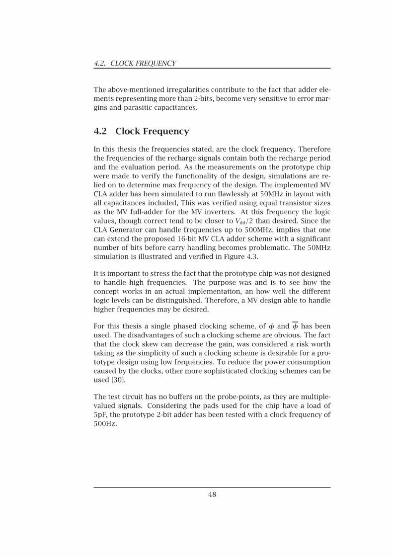
In this thesis the frequencies stated, are the clock frequency. Thereforethe frequencies of the recharge signals contain both the recharge periodand the evaluation period. As the measurements on the prototype chipwere made to verify the functionality of the design, simulations are re-lied on to determine max frequency of the design. The implemented MVCLA adder has been simulated to run flawlessly at 50MHz in layout withall capacitances included, This was verified using equal transistor sizesas the MV full-adder for the MV inverters. At this frequency the logicvalues, though correct tend to be closer to Vdd/2 than desired. Since theCLA Generator can handle frequencies up to 500MHz, implies that onecan extend the proposed 16-bit MV CLA adder scheme with a significantnumber of bits before carry handling becomes problematic. The 50MHzsimulation is illustrated and verified in Figure 4.3.
It is important to stress the fact that the prototype chip was not designedto handle high frequencies. The purpose was and is to see how theconcept works in an actual implementation, an how well the differentlogic levels can be distinguished. Therefore, a MV design able to handlehigher frequencies may be desired.
For this thesis a single phased clocking scheme, of φ and φ has beenused. The disadvantages of such a clocking scheme are obvious. The factthat the clock skew can decrease the gain, was considered a risk worthtaking as the simplicity of such a clocking scheme is desirable for a pro-totype design using low frequencies. To reduce the power consumptioncaused by the clocks, other more sophisticated clocking schemes can beused [30].
The test circuit has no buffers on the probe-points, as they are multiple-valued signals. Considering the pads used for the chip have a load of5pF, the prototype 2-bit adder has been tested with a clock frequency of500Hz.
48
4.3. POWER CONSUMPTION
0 0.05 0.1 0.15 0.2 0.25 0.3 0.35
0
0.5
1
1.5
2
Q −
R8
(V)
0 0.05 0.1 0.15 0.2 0.25 0.3 0.35
0
0.5
1
1.5
2
Sum
(V
)
0 0.05 0.1 0.15 0.2 0.25 0.3 0.35
0
0.5
1
1.5
2
Cou
t−in
v (V
)
time (µs)
Figure 4.3: Layout simulation of the MV CLA adder. The frequency is 50MHz.Q (radix-8 sum of X, Y and Cin), the radix-4 Sum and Cout are shown.
4.3 Power consumption
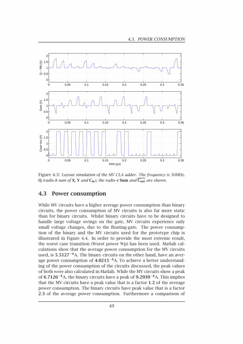
While MV circuits have a higher average power consumption than binarycircuits, the power consumption of MV circuits is also far more staticthan for binary circuits. Whilst binary circuits have to be designed tohandle large voltage swings on the gate, MV circuits experience onlysmall voltage changes, due to the floating-gate. The power consump-tion of the binary and the MV circuits used for the prototype chip isillustrated in Figure 4.4. In order to provide the most extreme result,the worst case transition (Worst power Wp) has been used. Matlab cal-culations show that the average power consumption for the MV circuitsused, is 5.5127−4A. The binary circuits on the other hand, have an aver-age power consumption of 4.0215−4A. To achieve a better understand-ing of the power consumption of the circuits discussed, the peak valuesof both were also calculated in Matlab. While the MV circuits show a peakof 6.7126−4A, the binary circuits have a peak of 9.2939−4A. This impliesthat the MV circuits have a peak value that is a factor 1.2 of the averagepower consumption. The binary circuits have peak value that is a factor2.3 of the average power consumption. Furthermore a comparison of
49
4.3. POWER CONSUMPTION
0 0.5 1 1.5 2 2.5 3−5
0
5
10x 10
−4
A
time (µs)
BinaryMultiple−value
Figure 4.4: The simulation illustrates the power consumption of the rechargeelements and the binary gates used in the MV CLA adder.
the peak amplitude values of the two different logics has been made.While the binary circuits used have a peak amplitude of 9.2938−4A, theMV circuits have a peak amplitude of 2.29−4A. This comparison furtherillustrates the static power consumption of MV circuits. The calculationsmade in Matlab, imply that binary circuits are best used for operationsthat are critical considering speed, like carry computation.
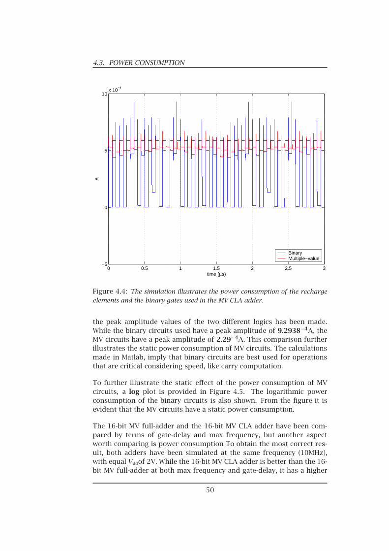
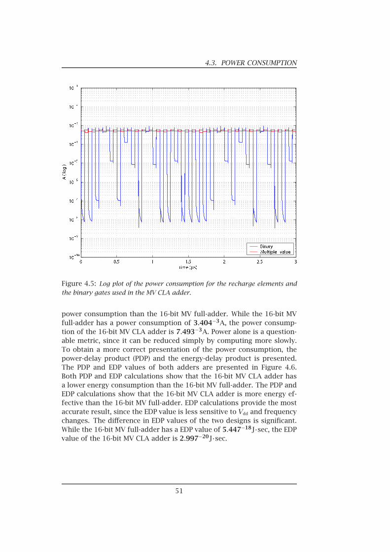
To further illustrate the static effect of the power consumption of MVcircuits, a log plot is provided in Figure 4.5. The logarithmic powerconsumption of the binary circuits is also shown. From the figure it isevident that the MV circuits have a static power consumption.
The 16-bit MV full-adder and the 16-bit MV CLA adder have been com-pared by terms of gate-delay and max frequency, but another aspectworth comparing is power consumption To obtain the most correct res-ult, both adders have been simulated at the same frequency (10MHz),with equal Vddof 2V. While the 16-bit MV CLA adder is better than the 16-bit MV full-adder at both max frequency and gate-delay, it has a higher
50
4.3. POWER CONSUMPTION
Figure 4.5: Log plot of the power consumption for the recharge elements andthe binary gates used in the MV CLA adder.
power consumption than the 16-bit MV full-adder. While the 16-bit MVfull-adder has a power consumption of 3.404−3A, the power consump-tion of the 16-bit MV CLA adder is 7.493−3A. Power alone is a question-able metric, since it can be reduced simply by computing more slowly.To obtain a more correct presentation of the power consumption, thepower-delay product (PDP) and the energy-delay product is presented.The PDP and EDP values of both adders are presented in Figure 4.6.Both PDP and EDP calculations show that the 16-bit MV CLA adder hasa lower energy consumption than the 16-bit MV full-adder. The PDP andEDP calculations show that the 16-bit MV CLA adder is more energy ef-fective than the 16-bit MV full-adder. EDP calculations provide the mostaccurate result, since the EDP value is less sensitive to Vdd and frequencychanges. The difference in EDP values of the two designs is significant.While the 16-bit MV full-adder has a EDP value of 5.447−18J·sec, the EDPvalue of the 16-bit MV CLA adder is 2.997−20J·sec.
51
4.4. THE PROTOTYPE DESIGN
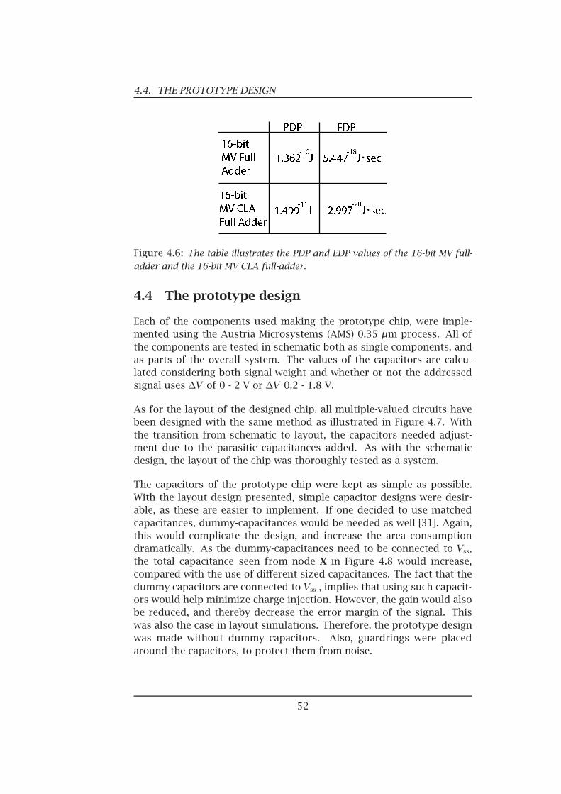
Figure 4.6: The table illustrates the PDP and EDP values of the 16-bit MV full-adder and the 16-bit MV CLA full-adder.
4.4 The prototype design
Each of the components used making the prototype chip, were imple-mented using the Austria Microsystems (AMS) 0.35 µm process. All ofthe components are tested in schematic both as single components, andas parts of the overall system. The values of the capacitors are calcu-lated considering both signal-weight and whether or not the addressedsignal uses ∆V of 0 - 2 V or ∆V 0.2 - 1.8 V.
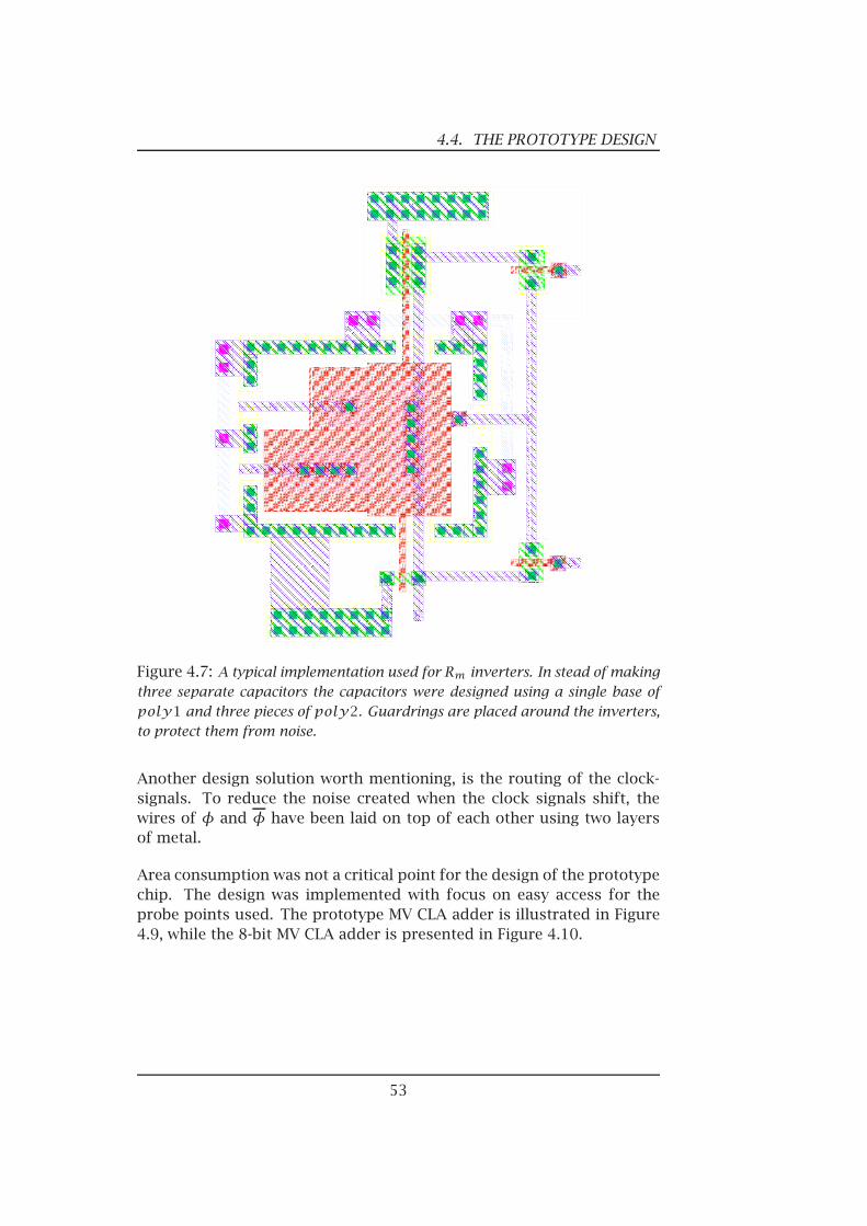
As for the layout of the designed chip, all multiple-valued circuits havebeen designed with the same method as illustrated in Figure 4.7. Withthe transition from schematic to layout, the capacitors needed adjust-ment due to the parasitic capacitances added. As with the schematicdesign, the layout of the chip was thoroughly tested as a system.
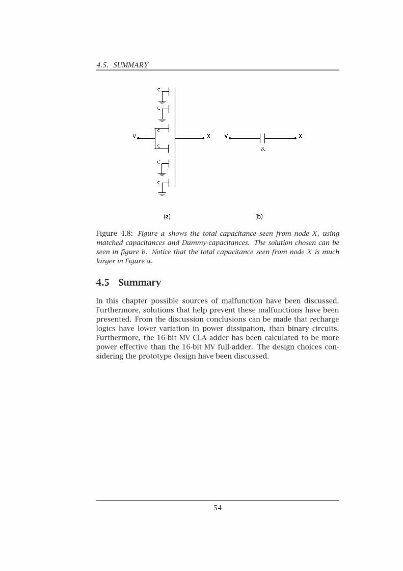
The capacitors of the prototype chip were kept as simple as possible.With the layout design presented, simple capacitor designs were desir-able, as these are easier to implement. If one decided to use matchedcapacitances, dummy-capacitances would be needed as well [31]. Again,this would complicate the design, and increase the area consumptiondramatically. As the dummy-capacitances need to be connected to Vss,the total capacitance seen from node X in Figure 4.8 would increase,compared with the use of different sized capacitances. The fact that thedummy capacitors are connected to Vss , implies that using such capacit-ors would help minimize charge-injection. However, the gain would alsobe reduced, and thereby decrease the error margin of the signal. Thiswas also the case in layout simulations. Therefore, the prototype designwas made without dummy capacitors. Also, guardrings were placedaround the capacitors, to protect them from noise.
52
4.4. THE PROTOTYPE DESIGN
Figure 4.7: A typical implementation used for Rm inverters. In stead of makingthree separate capacitors the capacitors were designed using a single base ofpoly1 and three pieces of poly2. Guardrings are placed around the inverters,to protect them from noise.
Another design solution worth mentioning, is the routing of the clock-signals. To reduce the noise created when the clock signals shift, thewires of φ and φ have been laid on top of each other using two layersof metal.
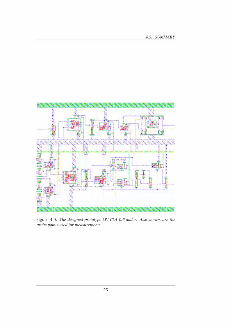
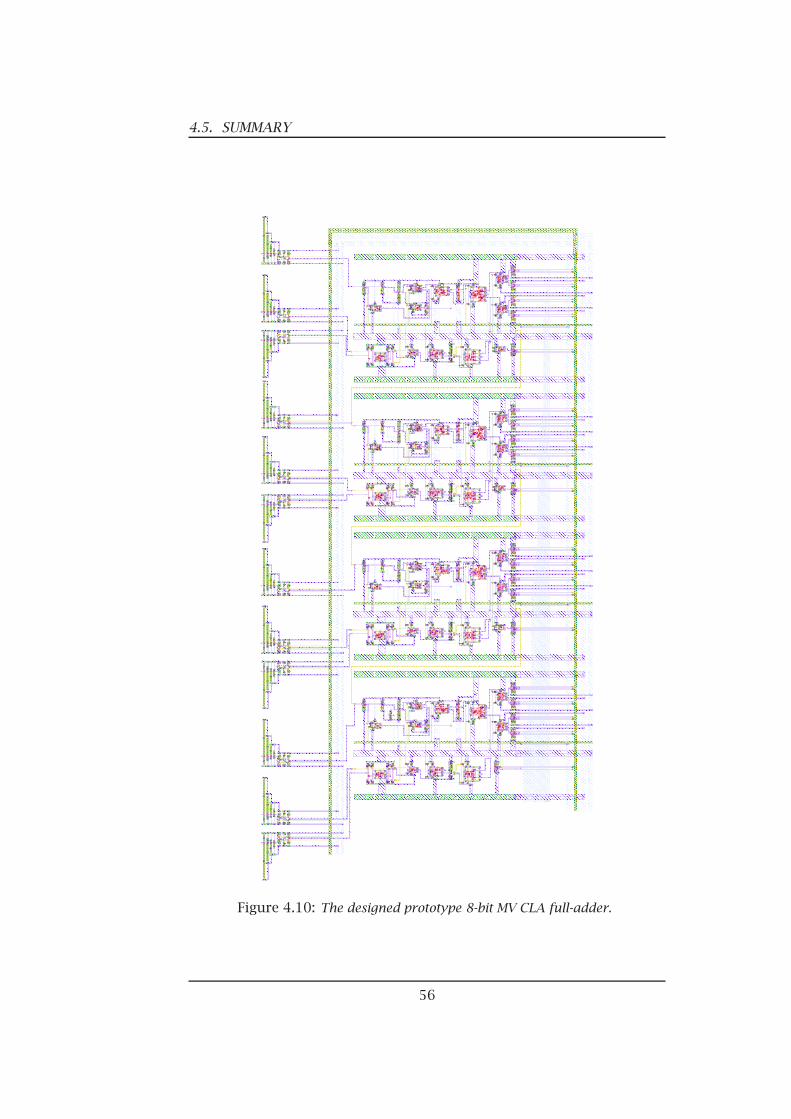
Area consumption was not a critical point for the design of the prototypechip. The design was implemented with focus on easy access for theprobe points used. The prototype MV CLA adder is illustrated in Figure4.9, while the 8-bit MV CLA adder is presented in Figure 4.10.
53
4.5. SUMMARY
Figure 4.8: Figure a shows the total capacitance seen from node X, usingmatched capacitances and Dummy-capacitances. The solution chosen can beseen in figure b. Notice that the total capacitance seen from node X is muchlarger in Figure a.
4.5 Summary
In this chapter possible sources of malfunction have been discussed.Furthermore, solutions that help prevent these malfunctions have beenpresented. From the discussion conclusions can be made that rechargelogics have lower variation in power dissipation, than binary circuits.Furthermore, the 16-bit MV CLA adder has been calculated to be morepower effective than the 16-bit MV full-adder. The design choices con-sidering the prototype design have been discussed.
54
4.5. SUMMARY
Figure 4.9: The designed prototype MV CLA full-adder. Also shown, are theprobe points used for measurements.
55
4.5. SUMMARY
Figure 4.10: The designed prototype 8-bit MV CLA full-adder.
56
Chapter 5
Conclusion and proposal forfurther work
In this thesis a voltage-mode multiple-valued recharge logic carry-look-ahead full-adder has been presented. The MV CLA full-adder includesthe use of floating-gate, or more precisely semi-floating-gate, as well asbinary gates. The operation of the semi-floating-gate is determined bythe weighed summation of voltage on the multiple input signals.
The essence of this thesis lies in the multiple-valued recharge carry-look-ahead scheme presented, as well as implementation of the prototypeCarry-Look-Ahead full-adder presented. Since the generated carry sig-nals are latched, these are not considered in the the gate-delay calcula-tions. Therefore the focus has been on the carry propagation generatedby a carry-in. A full implementation of the CLA scheme is presented inAppendix B. The circuits were fabricated in a CMOS 0.35µm process inorder to measure them on an actual ASIC.
5.1 Main contributions
The discoveries and ideas of the author of this thesis are presented inchapter three, with the proposed carry-look-ahead scheme as main con-tribution. The proposed scheme offers logic depth achieved with few ex-tra components, considering the propagating carry triggered by a carry-in.
5.2 Experimental Results
Each circuit was simulated as a single element and as a part of an overallsystem, and were proven to operate satisfyingly. Measurements show
57
5.3. FURTHER WORK
that there is a mismatch in the circuits, resulting in a recharge levelof 0.956V, as well as a mismatch in the voltage swing (∆V) of the logicvalues. Although a mismatch in the system was discovered, the adderworks satisfactory, with the exception of a single bit error on the outputof the MVBC used to convert the Sum. This bit error is caused by thelatch, used with the radix-4 Sum. The actual Sum is logically correct.Due to the MV circuits being sensitive to error margins and parasiticcapacitance, adder elements larger than 2-bit are not recomended.
The implementation of the presented 16-bit CLA scheme has showed tohave smaller gate-delay than the implementation of the 16-bit MV full-adder. It has been verified that the implemented MV CLA adder also canoperate on higher frequencies than the implemented MV full-adder, withboth adders designed with equal sized transistors. Furthermore, Matlabcalculations show that the implemented MV CLA full-adder has lowerPDP and EDP values than the implemented MV full-adder. This impliesthat the proposed MV CLA full-adder is more energy effective than theMV full-adder. It is therefore fair to state that a carry-look-ahead schemecan increase the performance of multiple-valued adders. Applying theproposed CLA scheme can therefore also lead to an increase in perform-ance for systems using MV SFG adders. While the implemented MV CLAadder has been simulated to operate at 50MHz, the implemented CLAGenerator is estimated to operate at frequencies up to 500MHz. It istherefore desireable to design MV adder elements capable to operate athigher frequencies than 50MHz, and thus exploit the potential of theCLA scheme better.
5.3 Further work
As the designed prototype adder has been proven to work, implement-ing it with the proposed carry-look-ahead scheme on a fabricated chipwould be worth exploring. Also implementing the proposed carry-look-ahead scheme in other applications that make use of the adders, e.g. amultiplier. Furthermore the proposed carry-look-ahead scheme could beimplemented in a decimator, also here providing a more effective carryhandling. Last but not least, publications could be made upon the dis-coveries made.
58

Appendix A
Truth tables
The truth tables presented here illustrate the input signal combinations(represented by node Z) used for testing the prototype adder. The firsttable illustrates the carry calculations with carry-in of 0, and the secondtable illustrates the carry calculation when carry-in is 1.
Z G P Platch Glatch PS=R CIn Cprop Glatch Cout0123
0000
0123
0001
1111
1110
1111
0000
0000
1111
1234
0001
1230
0010
1110
1101
1111
0000
0001
1110
2345
0011
2301
0101
1100
1011
1111
0000
0011
1100
3456
0111
3012
1011
1000
0111
1111
0000
0111
1000
Table A.1: The propagation of the carry-signal through the Carry Element,with a Carry-in signal = 0 is illustrated. The essential Bits described in the textare bold.
59
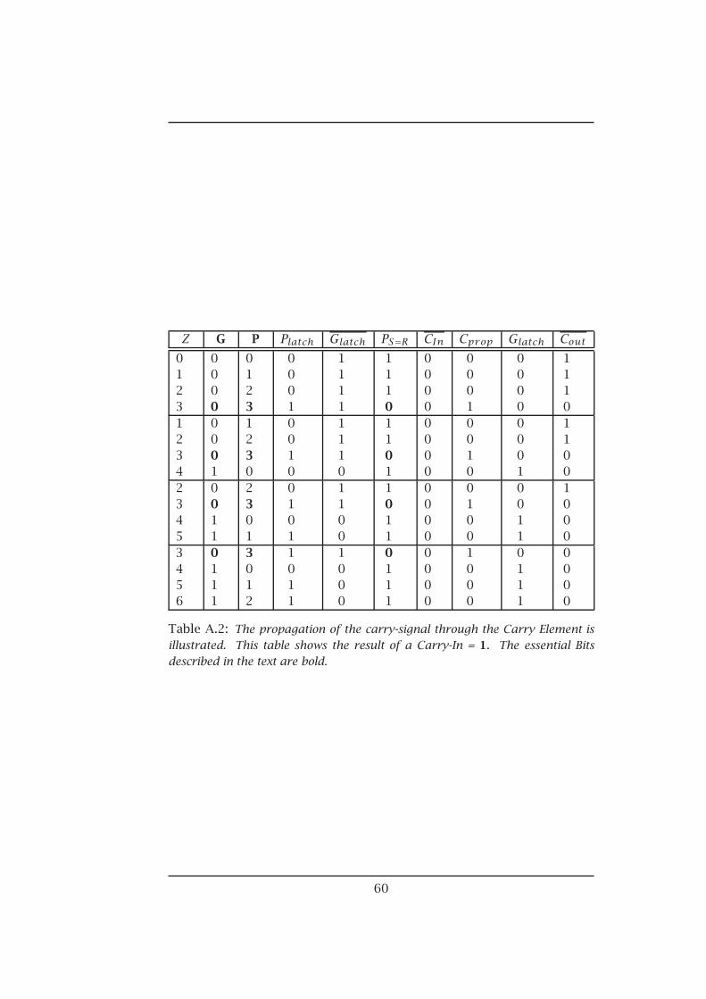
Z G P Platch Glatch PS=R CIn Cprop Glatch Cout0123
0000
0123
0001
1111
1110
0000
0001
0000
1110
1234
0001
1230
0010
1110
1101
0000
0010
0001
1100
2345
0011
2301
0101
1100
1011
0000
0100
0011
1000
3456
0111
3012
1011
1000
0111
0000
1000
0111
0000
Table A.2: The propagation of the carry-signal through the Carry Element isillustrated. This table shows the result of a Carry-In = 1. The essential Bitsdescribed in the text are bold.
60
Appendix B
Complete CLA proposal
B.1 A complete 16-bit MV CLA full-adder
A complete proposal of a 16-bit MV CLA full-adder is presented in Fig-ure B.1. This implementation has not been designed in either schem-atic or layout, due to time constraints. Although a presentation of thegates used to calculate the propagation of the generated carry signals isprovided.
The first NAND gate (NAND 1) Sums Glatched with PS=R. The reason forusing an inverted PS=R, is because PS=R is represented with inverted val-ues. The output of the first NAND gate is therefore 0 only when G is 1and PS=R is carry-sensitive. The second NAND gate used, combines allthree possible carry signals. The three signals are: a propagating carry-in, a generated carry from the first adder element or a generated carryfrom the second adder element. The output of this NAND gate is there-fore the carry-out of the two first adder elements. The third NAND gateused (NAND 3), combines the S = R signal from adder elements threeand four, with the inverted generated carry from adder element one. IfS = R of adder element three and four is carry sensitive, this is repres-ented with a logic 1. Therefore, to obtain the desired functionality, theinverted generated carry from adder element one needs to be invertedonce more. The output of the third NAND gate is 0 only when the firstadder element generates a carry, and the second, third and fourth adderelements are carry-sensitive. The fourth NAND gate (NAND 4) combinesthe generated carry from adder element one, with the generated carrysignals from adder elements two, three, four and an eventual propagat-ing carry-in. Thus the output of the fourth NAND gate is the carry-outof the four first adder elements. The fifth NAND gate used (NAND 5)combines the generated carry from adder element one with the two re-maining S = R signals, from adder elements five and six, and seven andeight respectively. The functionality is equal to NAND 3, therefore the
61
B.1. A COMPLETE 16-BIT MV CLA FULL-ADDER
generated carry needs to be inverted once more. The output of fifthNAND gate is 0 only when the remaining S = R are carry sensitive, and agenerated carry has passed the aforementioned gates. In the sixth NANDgate to be described, all generated carry signals are combined along withan eventual propagating carry-in. If any of the inputs of this NAND gateare 0, a carry-out is generated. The mentioned example counts for theother generated carry signals as well.
It is worth noticing that the gate delay of the generated carry from adderelement one, is 6∆G. Also, the worst gate-delay in the CLA Generator, thepath of the generated carry from adder element one to the carry-in onthe eight adder element, is 9∆G. Although a complicated structure, thegate-delay is still smaller than for the 16-bit MV full-adder. Time con-straints has been mentioned as one of the reasons why the proposeddesign has not been implemented in either schematics or layout. An-other reason is that due to the latching in the adder elements, gate-delaycalculations on the generated carry signals was considered to be unim-portant. Furthermore, the figure also illustrates that the proposed solu-tion increases the number of gates needed dramatically. If this solutionwas to be implemented as a 32-bit adder, the complexity would be evengreater. But since the CLA Generator makes use of binary gates, it willsustain high frequency. This will therefore not pose any delay for theadder elements used. A better solution concerning handling of the gen-erated carry signal may still be desired. It is therefore important to pointout that this is merely one proposed solution of the design.
62
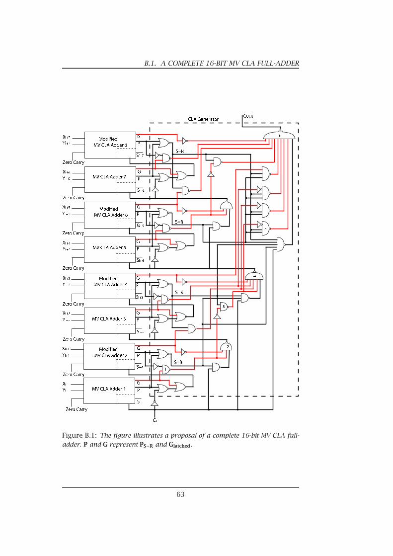
B.1. A COMPLETE 16-BIT MV CLA FULL-ADDER
Figure B.1: The figure illustrates a proposal of a complete 16-bit MV CLA full-adder. P and G represent PS=R and Glatched.
63

B.1. A COMPLETE 16-BIT MV CLA FULL-ADDER
64
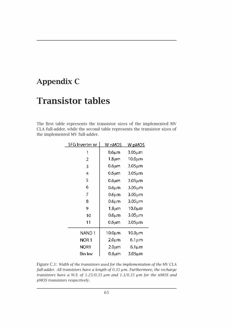
Appendix C
Transistor tables
The first table represents the transistor sizes of the implemented MVCLA full-adder, while the second table represents the transistor sizes ofthe implemented MV full-adder.
Figure C.1: Width of the transistors used for the implementation of the MV CLAfull-adder. All transistors have a length of 0.35 µm. Furthermore, the rechargetransistors have a W/L of 1.25/0.35 µm and 1.3/0.35 µm for the nMOS andpMOS transistors respectively.
65
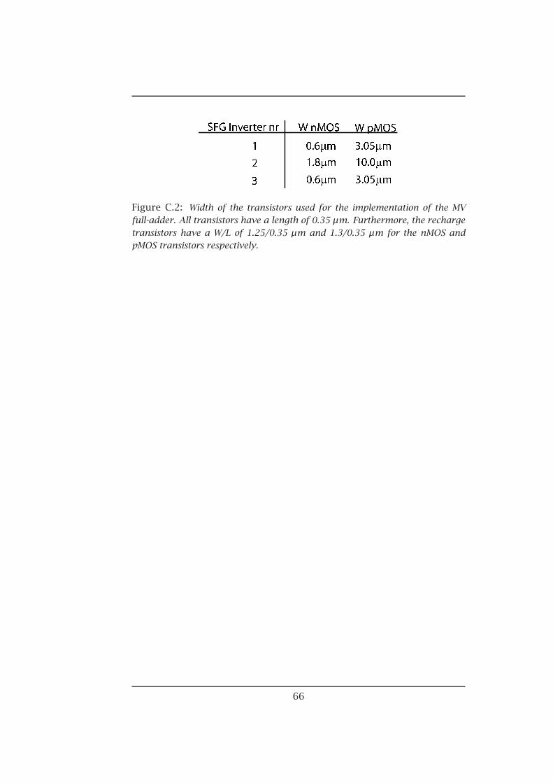
Figure C.2: Width of the transistors used for the implementation of the MVfull-adder. All transistors have a length of 0.35 µm. Furthermore, the rechargetransistors have a W/L of 1.25/0.35 µm and 1.3/0.35 µm for the nMOS andpMOS transistors respectively.
66
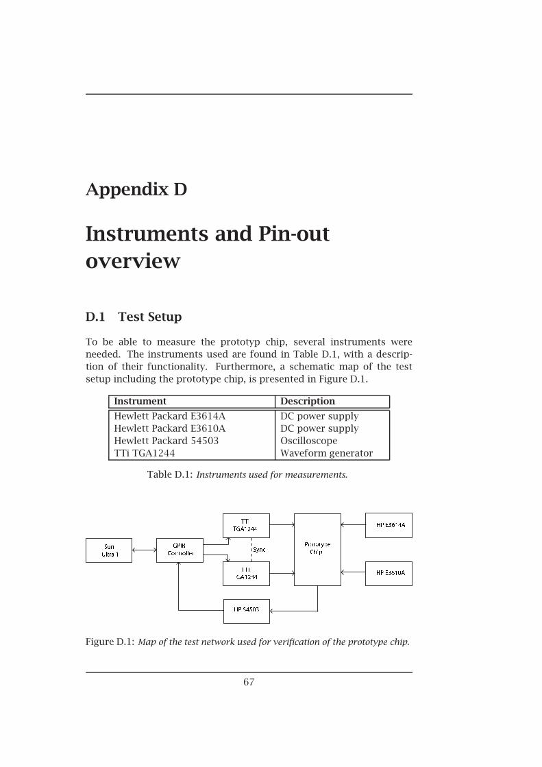
Appendix D
Instruments and Pin-outoverview
D.1 Test Setup
To be able to measure the prototyp chip, several instruments wereneeded. The instruments used are found in Table D.1, with a descrip-tion of their functionality. Furthermore, a schematic map of the testsetup including the prototype chip, is presented in Figure D.1.
Instrument Description
Hewlett Packard E3614AHewlett Packard E3610AHewlett Packard 54503TTi TGA1244
DC power supplyDC power supplyOscilloscopeWaveform generator
Table D.1: Instruments used for measurements.
Figure D.1: Map of the test network used for verification of the prototype chip.
67

D.2. PIN-OUT OVERVIEW
D.2 Pin-out overview
To provide easy access for measurements on the prototype chip, pin-outmaps are presented. The pin-out maps provide the input/output nameand the geographic position of these on the finished chip. Pin-out mapsto both prototype circuits are provided.
68

D.2. PIN-OUT OVERVIEW
Test Adder Description I/O Pin Out
PAD VssPAD Vdd
M5N5
VssVdd
A2B3
CLK’CLK
A1B2
Zero-CarryCarry-In
INClkCin
B1C2
Bit1Bit2Bit3Bit4
In1In2In3In4
C1D2D1E2
Output of AutoZero of Bit3 Out E1Output of BMVC using Bit3 & Bit4 as inputs Out F3Output of BMVC using Bit1 & Bit2 as inputs Out F2Node Z Out F1Output of G Out G2Output of P Out G3Output of Glatched Out G1Glatched Out H1PS=R Out H2Output of Carry-In inverted Out H3Cprop Out J1Glatched Out J2
COut Out K1Output of Bit1 Out K2Output of Bit0 Out L1Sumlatched Out L2Output of R4 inverter 2 Sum M1G (adder element) Out N1Q Out M2Output of Carry-In after AutoZero Out N2
Table D.2: Pin List for single adder, test element.
69
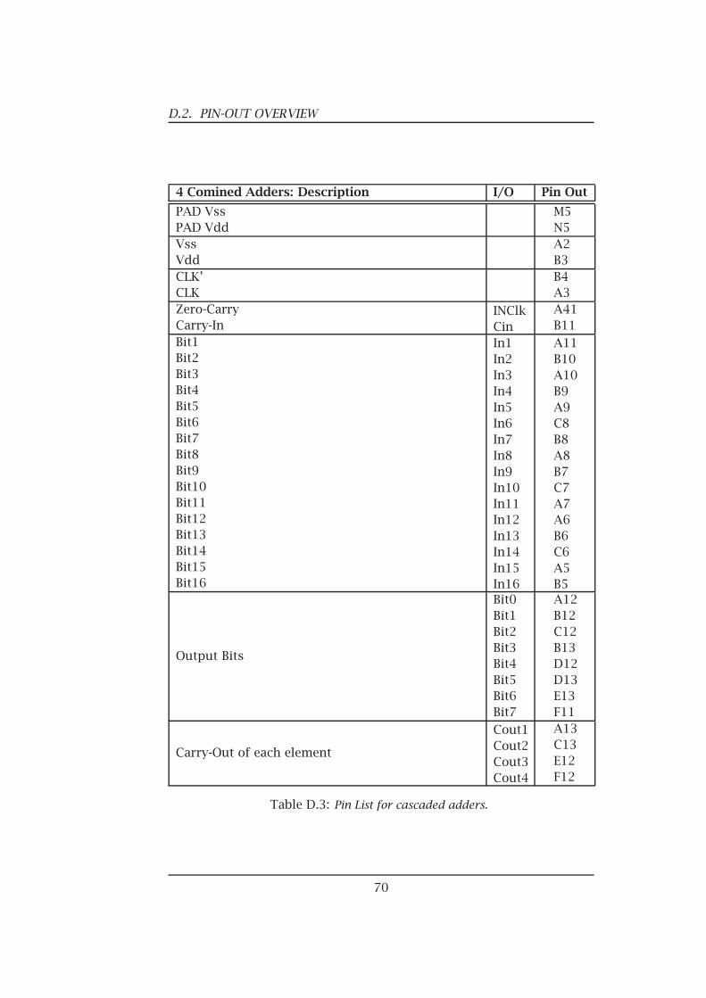
D.2. PIN-OUT OVERVIEW
4 Comined Adders: Description I/O Pin Out
PAD VssPAD Vdd
M5N5
VssVdd
A2B3
CLK’CLK
B4A3
Zero-CarryCarry-In
INClkCin
A41B11
Bit1Bit2Bit3Bit4Bit5Bit6Bit7Bit8Bit9Bit10Bit11Bit12Bit13Bit14Bit15Bit16
In1In2In3In4In5In6In7In8In9In10In11In12In13In14In15In16
A11B10A10B9A9C8B8A8B7C7A7A6B6C6A5B5
Output Bits
Bit0Bit1Bit2Bit3Bit4Bit5Bit6Bit7
A12B12C12B13D12D13E13F11
Carry-Out of each element
Cout1Cout2Cout3Cout4
A13C13E12F12
Table D.3: Pin List for cascaded adders.
70

Appendix E
Additional Figures
.tex In this section, additional layout figures are presented. Since mostcircuits used, resemble the two-input inverter presented in chapter four,only completely different designs are presented here. Furthermore, aplot of the prototype chip with pads is provided.
Figure E.1: The layout design of the AutoZero circuits used.
.tex
71
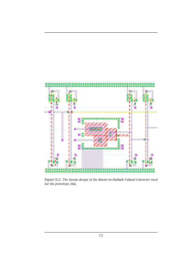
Figure E.2: The layout design of the Binary-to-Multiple-Valued Converter usedfor the prototype chip.
72
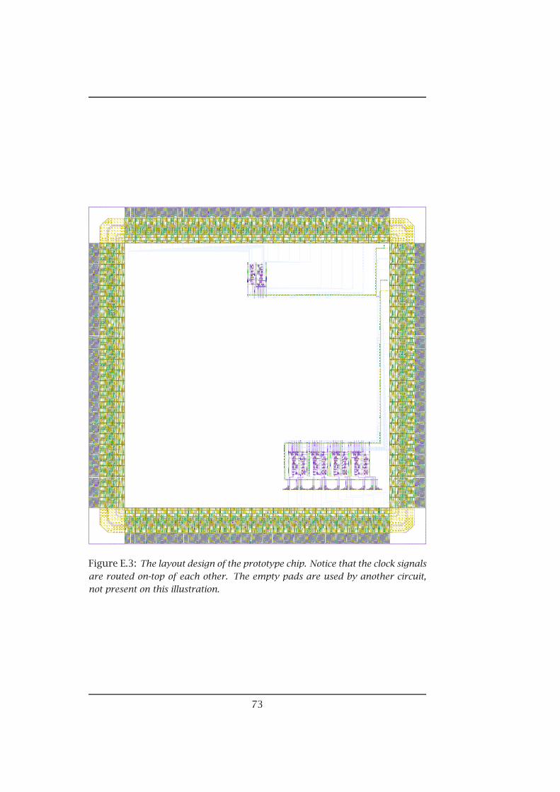
Figure E.3: The layout design of the prototype chip. Notice that the clock signalsare routed on-top of each other. The empty pads are used by another circuit,not present on this illustration.
73

74
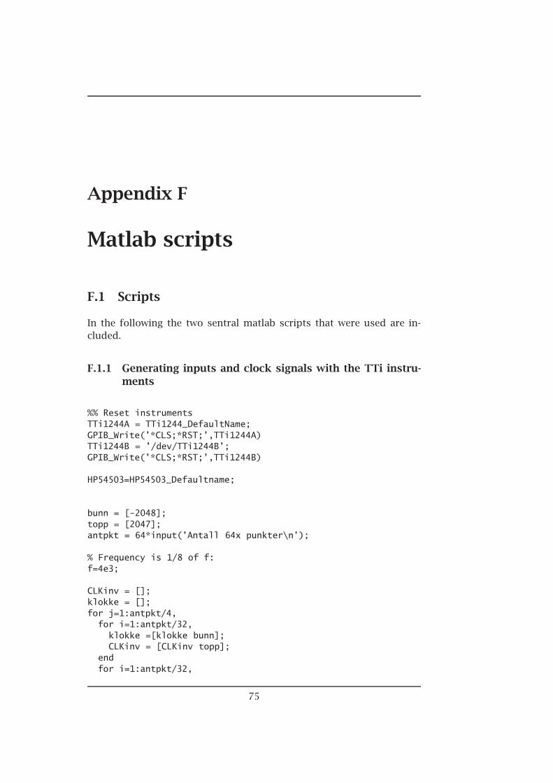
Appendix F
Matlab scripts
F.1 Scripts
In the following the two sentral matlab scripts that were used are in-cluded.
F.1.1 Generating inputs and clock signals with the TTi instru-ments
%% Reset instrumentsTTi1244A = TTi1244_DefaultName;GPIB_Write(’*CLS;*RST;’,TTi1244A)TTi1244B = ’/dev/TTi1244B’;GPIB_Write(’*CLS;*RST;’,TTi1244B)
HP54503=HP54503_Defaultname;
bunn = [-2048];topp = [2047];antpkt = 64*input(’Antall 64x punkter\n’);
% Frequency is 1/8 of f:f=4e3;
CLKinv = [];klokke = [];for j=1:antpkt/4,
for i=1:antpkt/32,klokke =[klokke bunn];CLKinv = [CLKinv topp];
endfor i=1:antpkt/32,
75
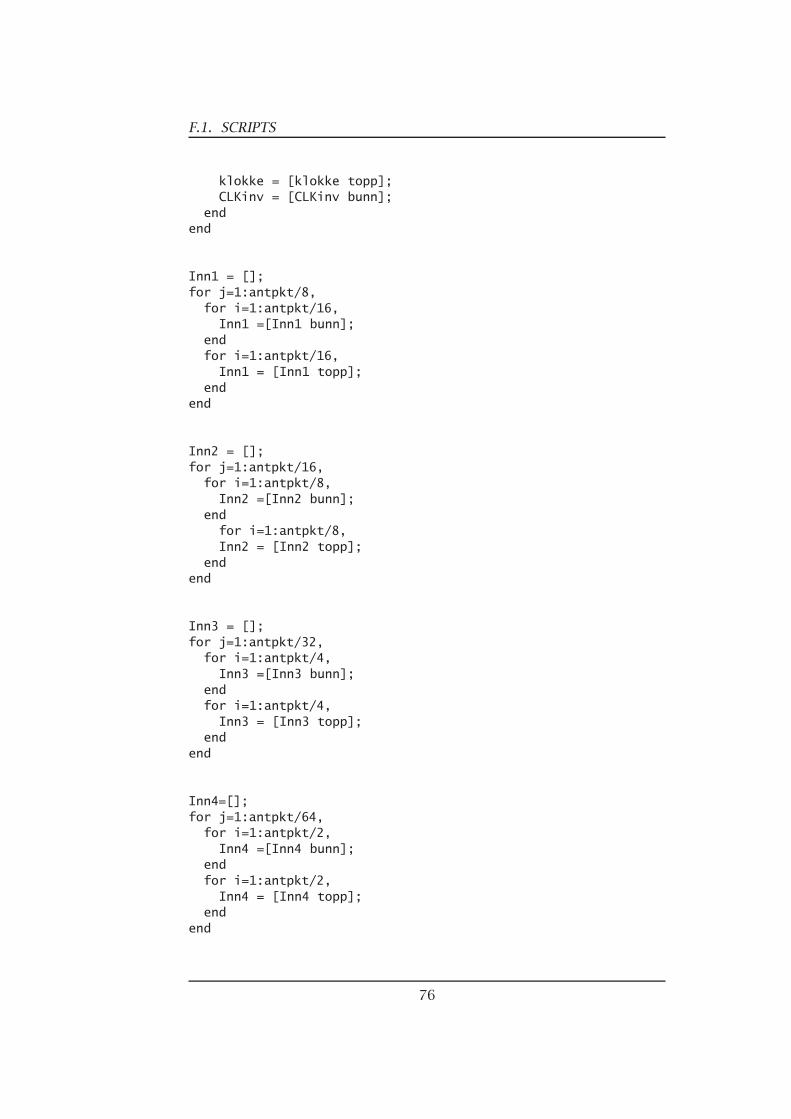
F.1. SCRIPTS
klokke = [klokke topp];CLKinv = [CLKinv bunn];
endend
Inn1 = [];for j=1:antpkt/8,
for i=1:antpkt/16,Inn1 =[Inn1 bunn];
endfor i=1:antpkt/16,
Inn1 = [Inn1 topp];end
end
Inn2 = [];for j=1:antpkt/16,
for i=1:antpkt/8,Inn2 =[Inn2 bunn];
endfor i=1:antpkt/8,Inn2 = [Inn2 topp];
endend
Inn3 = [];for j=1:antpkt/32,
for i=1:antpkt/4,Inn3 =[Inn3 bunn];
endfor i=1:antpkt/4,
Inn3 = [Inn3 topp];end
end
Inn4=[];for j=1:antpkt/64,
for i=1:antpkt/2,Inn4 =[Inn4 bunn];
endfor i=1:antpkt/2,
Inn4 = [Inn4 topp];end
end
76
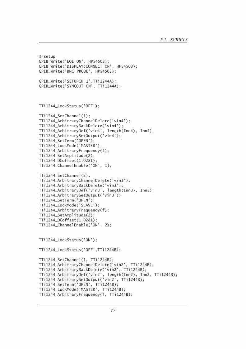
F.1. SCRIPTS
% setupGPIB_Write(’EOI ON’, HP54503);GPIB_Write(’DISPLAY:CONNECT ON’, HP54503);GPIB_Write(’BNC PROBE’, HP54503);
GPIB_Write(’SETUPCH 1’,TTi1244A);GPIB_Write(’SYNCOUT ON’, TTi1244A);
TTi1244_LockStatus(’OFF’);
TTi1244_SetChannel(1);TTi1244_ArbitraryChannelDelete(’vin4’);TTi1244_ArbitraryBackDelete(’vin4’);TTi1244_ArbitraryDef(’vin4’, length(Inn4), Inn4);TTi1244_ArbitrarySetOutput(’vin4’);TTi1244_SetTerm(’OPEN’);TTi1244_LockMode(’MASTER’);TTi1244_ArbitraryFrequency(f);TTi1244_SetAmplitude(2);TTi1244_DCoffset(1.0281);TTi1244_ChannelEnable(’ON’, 1);
TTi1244_SetChannel(2);TTi1244_ArbitraryChannelDelete(’vin3’);TTi1244_ArbitraryBackDelete(’vin3’);TTi1244_ArbitraryDef(’vin3’, length(Inn3), Inn3);TTi1244_ArbitrarySetOutput(’vin3’);TTi1244_SetTerm(’OPEN’);TTi1244_LockMode(’SLAVE’);TTi1244_ArbitraryFrequency(f);TTi1244_SetAmplitude(2);TTi1244_DCoffset(1.0281);TTi1244_ChannelEnable(’ON’, 2);
TTi1244_LockStatus(’ON’);
TTi1244_LockStatus(’OFF’,TTi1244B);
TTi1244_SetChannel(1, TTi1244B);TTi1244_ArbitraryChannelDelete(’vin2’, TTi1244B);TTi1244_ArbitraryBackDelete(’vin2’, TTi1244B);TTi1244_ArbitraryDef(’vin2’, length(Inn2), Inn2, TTi1244B);TTi1244_ArbitrarySetOutput(’vin2’, TTi1244B);TTi1244_SetTerm(’OPEN’, TTi1244B);TTi1244_LockMode(’MASTER’, TTi1244B);TTi1244_ArbitraryFrequency(f, TTi1244B);
77
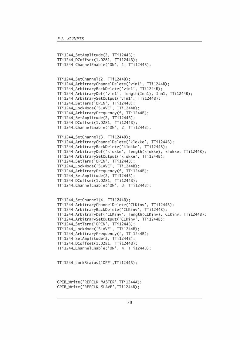
F.1. SCRIPTS
TTi1244_SetAmplitude(2, TTi1244B);TTi1244_DCoffset(1.0281, TTi1244B);TTi1244_ChannelEnable(’ON’, 1, TTi1244B);
TTi1244_SetChannel(2, TTi1244B);TTi1244_ArbitraryChannelDelete(’vin1’, TTi1244B);TTi1244_ArbitraryBackDelete(’vin1’, TTi1244B);TTi1244_ArbitraryDef(’vin1’, length(Inn1), Inn1, TTi1244B);TTi1244_ArbitrarySetOutput(’vin1’, TTi1244B);TTi1244_SetTerm(’OPEN’, TTi1244B);TTi1244_LockMode(’SLAVE’, TTi1244B);TTi1244_ArbitraryFrequency(f, TTi1244B);TTi1244_SetAmplitude(2, TTi1244B);TTi1244_DCoffset(1.0281, TTi1244B);TTi1244_ChannelEnable(’ON’, 2, TTi1244B);
TTi1244_SetChannel(3, TTi1244B);TTi1244_ArbitraryChannelDelete(’klokke’, TTi1244B);TTi1244_ArbitraryBackDelete(’klokke’, TTi1244B);TTi1244_ArbitraryDef(’klokke’, length(klokke), klokke, TTi1244B);TTi1244_ArbitrarySetOutput(’klokke’, TTi1244B);TTi1244_SetTerm(’OPEN’, TTi1244B);TTi1244_LockMode(’SLAVE’, TTi1244B);TTi1244_ArbitraryFrequency(f, TTi1244B);TTi1244_SetAmplitude(2, TTi1244B);TTi1244_DCoffset(1.0281, TTi1244B);TTi1244_ChannelEnable(’ON’, 3, TTi1244B);
TTi1244_SetChannel(4, TTi1244B);TTi1244_ArbitraryChannelDelete(’CLKinv’, TTi1244B);TTi1244_ArbitraryBackDelete(’CLKinv’, TTi1244B);TTi1244_ArbitraryDef(’CLKinv’, length(CLKinv), CLKinv, TTi1244B);TTi1244_ArbitrarySetOutput(’CLKinv’, TTi1244B);TTi1244_SetTerm(’OPEN’, TTi1244B);TTi1244_LockMode(’SLAVE’, TTi1244B);TTi1244_ArbitraryFrequency(f, TTi1244B);TTi1244_SetAmplitude(2, TTi1244B);TTi1244_DCoffset(1.0281, TTi1244B);TTi1244_ChannelEnable(’ON’, 4, TTi1244B);
TTi1244_LockStatus(’OFF’,TTi1244B);
GPIB_Write(’REFCLK MASTER’,TTi1244A);GPIB_Write(’REFCLK SLAVE’,TTi1244B);
78
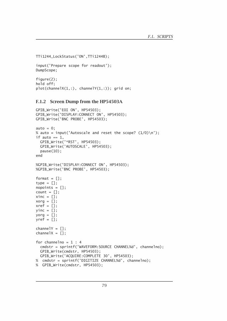
F.1. SCRIPTS
TTi1244_LockStatus(’ON’,TTi1244B);
input(’Prepare scope for readout’);DumpScope;
figure(2);hold off;plot(channelX(1,:), channelY(1,:)); grid on;
F.1.2 Screen Dump from the HP54503A
GPIB_Write(’EOI ON’, HP54503);GPIB_Write(’DISPLAY:CONNECT ON’, HP54503);GPIB_Write(’BNC PROBE’, HP54503);
auto = 0;% auto = input(’Autoscale and reset the scope? (1/0)\n’);if auto == 1,
GPIB_Write(’*RST’, HP54503);GPIB_Write(’AUTOSCALE’, HP54503);pause(10);
end
%GPIB_Write(’DISPLAY:CONNECT ON’, HP54503);%GPIB_Write(’BNC PROBE’, HP54503);
format = [];type = [];nopoints = [];count = [];xinc = [];xorg = [];xref = [];yinc = [];yorg = [];yref = [];
channelY = [];channelX = [];
for channelno = 1 : 4cmdstr = sprintf(’WAVEFORM:SOURCE CHANNEL%d’, channelno);GPIB_Write(cmdstr, HP54503);GPIB_Write(’ACQUIRE:COMPLETE 30’, HP54503);
% cmdstr = sprintf(’DIGITIZE CHANNEL%d’, channelno);% GPIB_Write(cmdstr, HP54503);
79
F.1. SCRIPTS
GPIB_Write(’SYSTEM:HEADER OFF’, HP54503);GPIB_Write(’WAVEFORM:PREAMBLE?’, HP54503);data = GPIB_Read(HP54503);
% vectorize comma-separated data in string.% data - input string% tmp - vectorized data
tmp = [0:9];k = 1;j = [];for i = 1 : length(data)
if data(i) ~= ’,’,j = [j data(i)];
endif data(i) == ’,’,
tmp(k) = str2num(j);k = k + 1;j = [];
endend%tmp(k) = str2num(j);
format(channelno) = tmp(1);type(channelno) = tmp(2);nopoints(channelno) = tmp(3);count(channelno) = tmp(4);xinc(channelno) = tmp(5);xorg(channelno) = tmp(6);xref(channelno) = tmp(7);yinc(channelno) = tmp(8);yorg(channelno) = tmp(9);yref(channelno) = tmp(10);
GPIB_Write(’WAVEFORM:FORMAT ASCII’, HP54503);GPIB_Write(’WAVEFORM:DATA?’, HP54503);b = GPIB_Read(HP54503);
array = [1:500];k = 1;j = [];for i = 1 : length(b)
%b(i)if b(i) ~= ’,’
j = [j b(i)];endif b(i) == ’,’
80
F.1. SCRIPTS
array(k) = str2num(j);k = k + 1;j = [];
endend
%plot(array)
y = array;
for i = 1 : length(y)y(i) = (y(i) - yref(channelno))*yinc(channelno) + yorg(channelno);
end
channelY(channelno, :) = y;
x = [0:499];for i = 1 : length(y)
x(i) = (x(i) - xref(channelno))*xinc(channelno) + xorg(channelno);end
channelX(channelno, :) = x;
% figure(channelno*10000);% plot(x, y); grid on;
end
figure(100);subplot(4,1,1), plot(channelX(1,:), channelY(1,:)); grid on;subplot(4,1,2), plot(channelX(2,:), channelY(2,:)); grid on;subplot(4,1,3), plot(channelX(3,:), channelY(3,:)); grid on;subplot(4,1,4), plot(channelX(4,:), channelY(4,:)); grid on;
%axis([-0.025 0.025 -0.1 2.1]);date = clock;date2 = sprintf(’%d.%d.%d’, date(3), date(2), date(1));ylabel(’Out (V)’);
81

F.1. SCRIPTS
82
Appendix G
Additional Simulations
Figure G.1: Layout simulation of the the carry element of the adder. TheZeroCarry is equal to the clock signal used. The ZeroCarry, Xi and Yi are summed,resulting in the R8 signal (Z). The R8 signal is used to determine the internalcarry (G), which in turn is summed with the latter to give us the R4 signal (P).The frequency is 10MHz.
83
Figure G.2: Layout simulation of the carry element of the adder. The internalcarry (G) is latched with the R4 signal (P), resulting in the latched representationof (P), namely (Platched). The frequency is 10MHz.
84
Figure G.3: Layout simulation of the carry element of the adder. The internalcarry (G) is inverted (G), and then latched. The frequency is 10MHz.
85
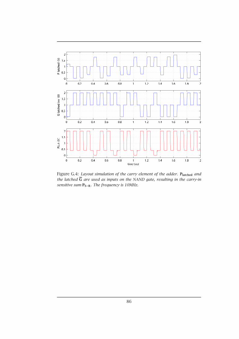
Figure G.4: Layout simulation of the carry element of the adder. Platched andthe latched G are used as inputs on the NAND gate, resulting in the carry-insensitive sum PS=R. The frequency is 10MHz.
86
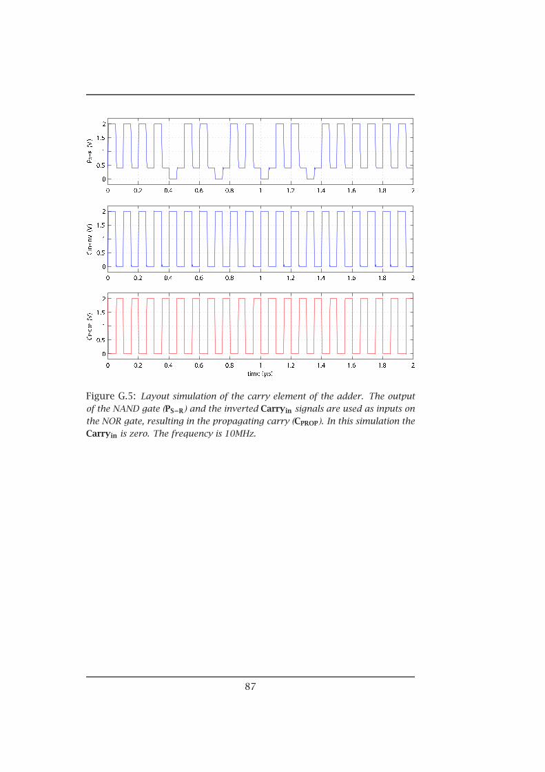
Figure G.5: Layout simulation of the carry element of the adder. The outputof the NAND gate (PS=R) and the inverted Carryin signals are used as inputs onthe NOR gate, resulting in the propagating carry (CPROP). In this simulation theCarryin is zero. The frequency is 10MHz.
87
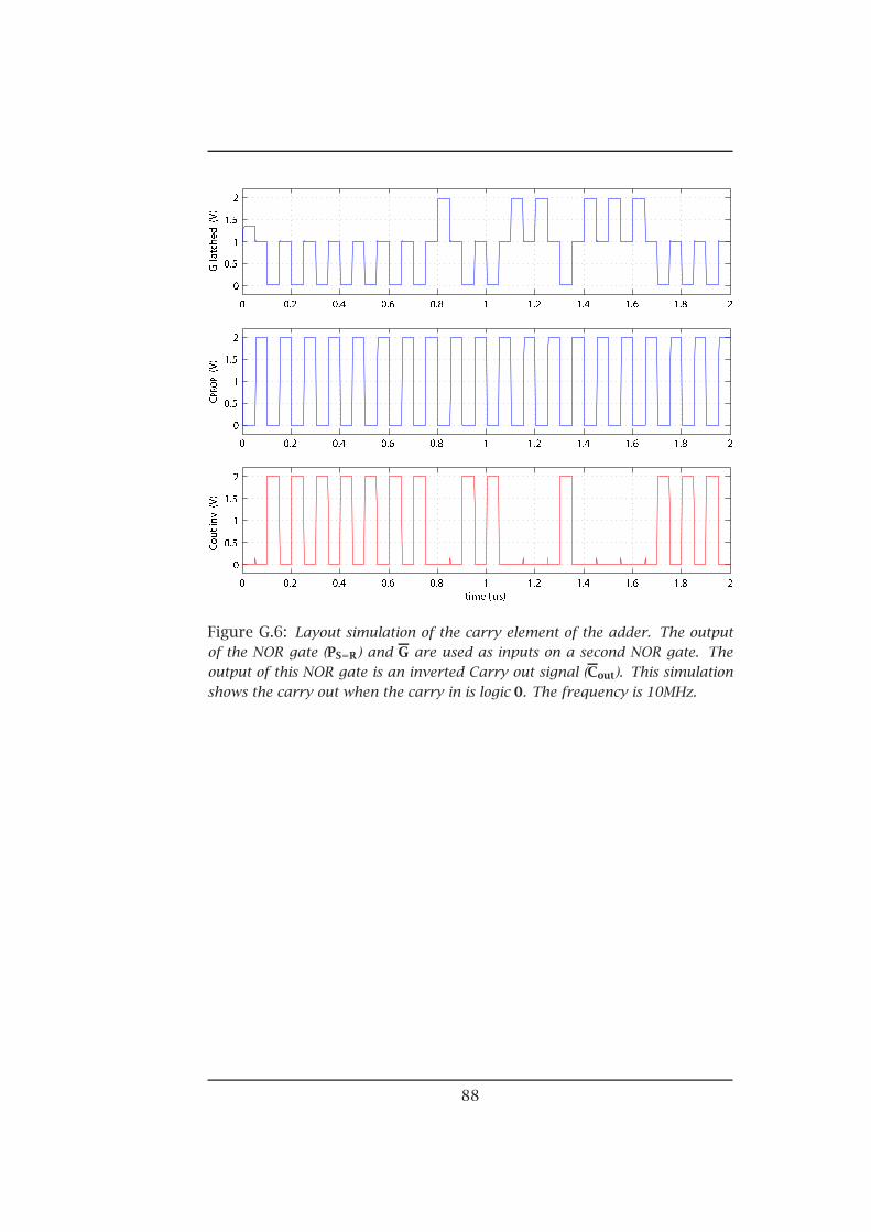
Figure G.6: Layout simulation of the carry element of the adder. The outputof the NOR gate (PS=R) and G are used as inputs on a second NOR gate. Theoutput of this NOR gate is an inverted Carry out signal (Cout). This simulationshows the carry out when the carry in is logic 0. The frequency is 10MHz.
88
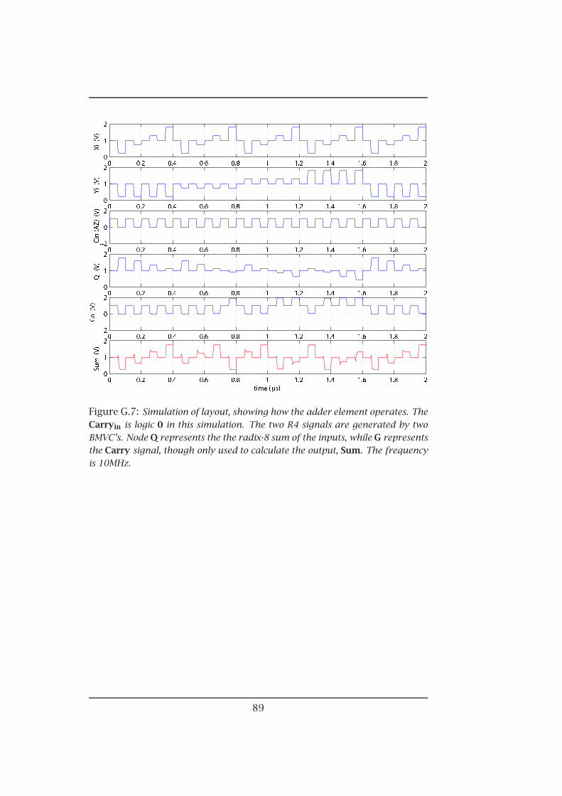
Figure G.7: Simulation of layout, showing how the adder element operates. TheCarryin is logic 0 in this simulation. The two R4 signals are generated by twoBMVC’s. Node Q represents the the radix-8 sum of the inputs, while G representsthe Carry signal, though only used to calculate the output, Sum. The frequencyis 10MHz.
89
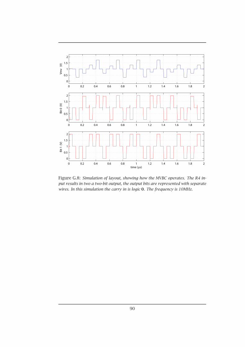
0 0.2 0.4 0.6 0.8 1 1.2 1.4 1.6 1.8 2
0
0.5
1
1.5
2
Vmv
(V)
0 0.2 0.4 0.6 0.8 1 1.2 1.4 1.6 1.8 2
0
0.5
1
1.5
2
Bit 0
(V)
0 0.2 0.4 0.6 0.8 1 1.2 1.4 1.6 1.8 2
0
0.5
1
1.5
2
Bit 1
(V)
time (µs)
Figure G.8: Simulation of layout, showing how the MVBC operates. The R4 in-put results in two a two-bit output, the output bits are represented with separatewires. In this simulation the carry in is logic 0. The frequency is 10MHz.
90
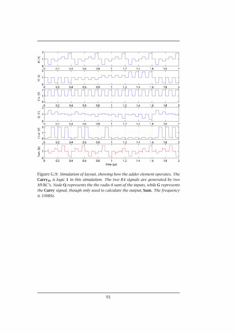
Figure G.9: Simulation of layout, showing how the adder element operates. TheCarryin is logic 1 in this simulation. The two R4 signals are generated by twoMVBC’s. Node Q represents the the radix-8 sum of the inputs, while G representsthe Carry signal, though only used to calculate the output, Sum. The frequencyis 10MHz.
91
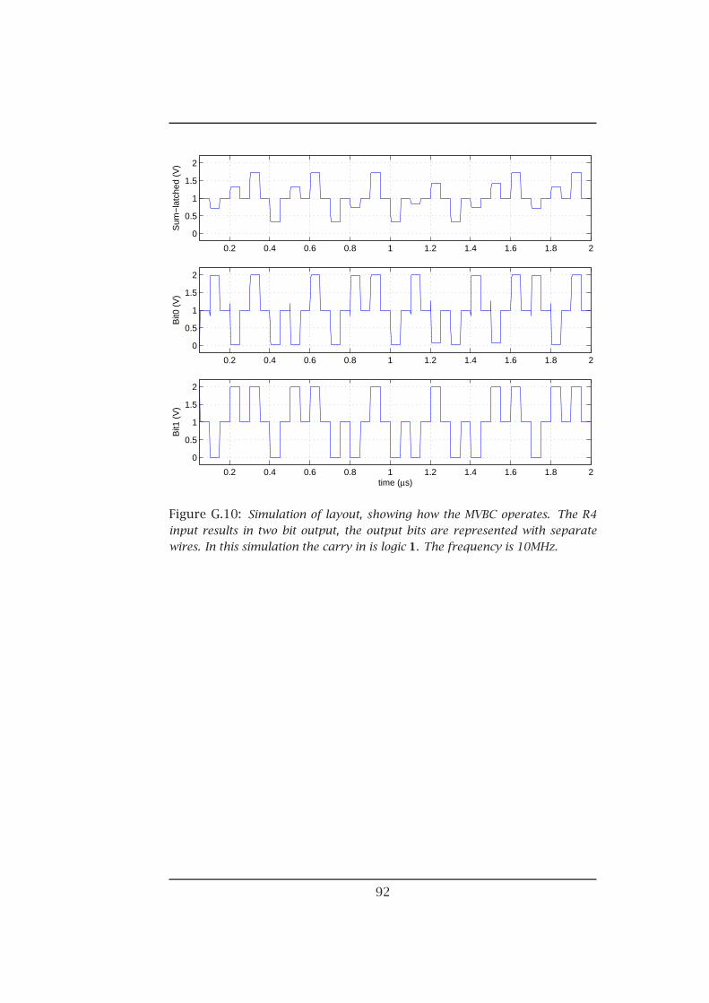
0.2 0.4 0.6 0.8 1 1.2 1.4 1.6 1.8 2
0
0.5
1
1.5
2S
um−
latc
hed
(V)
0.2 0.4 0.6 0.8 1 1.2 1.4 1.6 1.8 2
0
0.5
1
1.5
2
Bit0
(V
)
0.2 0.4 0.6 0.8 1 1.2 1.4 1.6 1.8 2
0
0.5
1
1.5
2
Bit1
(V
)
time (µs)
Figure G.10: Simulation of layout, showing how the MVBC operates. The R4input results in two bit output, the output bits are represented with separatewires. In this simulation the carry in is logic 1. The frequency is 10MHz.
92
Appendix H
Glossary
AMS Austria MikrosystemeAZ Auto-Zero
BMVC Binary-to-Multiple-Valued ConverterCLA Carry-Look-Ahead
CMOS Complementary Metal-Oxide-SiliconEDP Energy-Delay-ProductFG Floating-GateLSB Least Significant BitMOS Metal-Oxide-Silicon
MOSFET Metal-Oxide-Silicon Field Effect TransistorMSB Most Significant BitMV Multiple-Valued
MVBC Multiple-Valued-to-Binary ConverterMVL Multiple-Valued LogicPDP Power-Delay-ProductSFG Semi-Floating-GateTm Typical-mean
UVFG Ultra-Violet Floating-GateWo Worst oneWz Worst zero
93

94
BIBLIOGRAPHY
Bibliography
[1] I. Koren “Computer Arithmetic Algorithms” , A. K. Peters Ltd,Second edition, 2002, pp. 95-99 & pp. 106-109.
[2] K. Raahemifar, and M. Ahmadi, “Fast Carry-Look-Ahead Adder”, Pro-ceedings of the 1999 IEEE Canadian Conference on Electrical andComputer Engineering, pp. 529-532.
[3] G. A. Ruiz, and M. A. Manzano, “Compact 32-bit CMOS Adder inMultiple-Output DCVS Logic for Self-Timed Circuits”, IEE Proc.-Circuits Devices Syst., vol. 147, no. 3, June 2000.
[4] Y. T. Lee, I. C. Park and C. M. Kyung, “Design of Compact Static CMOSCarry Look-Ahead Adder using Recursicve Output Property”, Elec-tronics Letters 29th April 1993, vol. 29, no9 pp. 794-796.
[5] K. Ueda, H. Suzuki, K. Suda, H. Shinohara and K. Mashiko, “A 64-bit Carry Look-Ahead Adder using Pass Transistor BiCMOS Gates”,IEEE Journal of Solid-State Circuits, vol. 31, no. 6, pp. 810-818, June1996.
[6] K. Ueda, H. Suzuki, K. Suda, H. Shinohara and K. Mashiko, “A 64-bit Carry Look-Ahead Adder using Pass Transistor BiCMOS Gates”,IEEE Journal of Solid-State Circuits, vol. 31, no. 6, June 1996.
[7] H. Y. Huang, and T. N. Wang, “High-Speed CMOS Logic Circuits inCapacitor Coupling Technique”, The 2001 IEEE International Sym-posium on Circuits and Systems, vol. 4, pp. 634-637, 6-9 May 2001,ISCAS 2001.
[8] Tadashi Shibata and Tadahiro. Ohmi, “A Functional MOS TransistorFeaturing Gate-Level Weighed Sum and Threshold Operations”,IEEE Transactions on Electron Devices, vol. 39, no. 6. pp 1444-1455,June 1992.
[9] Tadashi Shibata and Tadahiro. Ohmi, “Neuron MOS Binary-Logic In-tegrated Circuits-Part I: Design Fundamentals and Soft-Hardware-Logic Circuit Implementation”, IEEE Transactions on ElectronDevices, vol. 40, no. 3. pp 570-576, March 1993.
95
BIBLIOGRAPHY
[10] Tadashi Shibata and Tadahiro. Ohmi, “Neuron MOS Binary-LogicIntegrated Circuits-Part II: Simplifying Tecniques of Circuit Con-figuration and their Practical Applications”, IEEE Transactions onElectron Devices, vol. 40, no. 5. pp 974-979, May 1993.
[11] J. Shen, K. Tanno, O. Ishizuka and Z. Tang, “Neuron-MOS currentmirror circuit and its application to multi-valued logic” , IEICE, Vol.E82-D, No. 5, pp. 940-948, May 1999.
[12] Y. Berg, T.S. Lande, Ø. Næss, and H. Gundersen, “Ultra-low-VoltageFloating-Gate Transconductance Amplifiers”, IEEE Transactions onCircuits and Systems-II: Analog and Digital Signal Processing, Vol. 48,No. 1, pp. 37-44, January 2001.
[13] Y. Berg, O. Næss, and M. Høvin, “Ultra lowvoltage floating-gatetransconductance amplifier”, ISCAS 2000, IEEE International Sym-posium in Circuits and Systems, May 28-31, 2000.
[14] Y. Berg, D. T. Wisland, and T. S. Lande, “Ultra Low-Voltage/Low-Power Digital Floating-Gate Circuits”, IEEE International Symposiumin Circuits and Systems-II: Analog and Digital Signal Processing, vol.46, no.7, July 1999.
[15] Y. Berg, T. S. Lande, O. Næss and H. Gundersen, “Ultra-Low-Voltage Floating-Gate Transconductance Amplifiers”, IEEE Interna-tional Symposium in Circuits and Systems-II: Analog and Digital Sig-nal Processing, vol. 48, no.1, January 2001.
[16] S. Aunet, Y. Berg and T. Sæther, “Real-Time Reconfigurable Lin-ear Threshold Elements Implemented in Floating-Gate CMOS”, IEEETransactions on Neural Networks , vol. 14, no.5, September 2003.
[17] Y. Berg, T. S. Lande and O. Næss, “Programming Floating-Gate Cir-cuits with UV-Activated Conductances”, IEEE Transactions on Cir-cuits and Systems-II: Analog and Digital Signal Processing, vol. 48,no. 1, January 2001.
[18] Koji Kotani, Tadashi Shibata, Makoto Imai and Tadahiro. Ohmi,“Clock-Controlled Neuron-MOS Logic Gates”, IEEE Transactions onCircuits and Systems II: Analog and Digital Signal Processing, vol. 45,no. 4. pp 518-522, April 1998.
[19] O. Mirmotahari and Y. Berg, “A novel multiple-input multiple-valued semi-floating-gate latch”, Proc. IEEE International Sym-posium on Circuits and Systems, vol. 2, pp. II-592–II-595, May, 2002.
[20] O. Mirmotahari, “Novel Latching Scheme in Multiple-Valued Re-charge Logic”, Cand. Scient. Thesis, May, 2003.
96
BIBLIOGRAPHY
[21] P. Hafliger and H.K. Riis, “A Multi-Level Static Memory Cell” , IEEE,International Symposium Circuits and Systems, 2004. ISCAS 2004,Vol. 5, pp 393-396, 23-26 May 2004.
[22] H.K. Riis, and P. Hafliger, “Spike based learning with weak multi-level static memory” , IEEE, Proceedings of the 2003 InternationalSymposium Circuits and Systems. ISCAS 2003, Vol. 1, pp 25-28, May2003.
[23] Paul R. Gray, and Robert G. Meyer, “Analysis an design of AnalogIntegrated Circuits” , John Wiley & Sons, Second edition, 1984.
[24] Y. Berg, S. Aunet, Ø. Næss, O. Mirmotahari and M. Høvin, “Binary toMultiple-Valued Recharge Converter for Multiple-Valued CMOS Lo-gic”, The 16th European Conference on Circuits Theory and Design,ECCTD’03, Krakow, Poland.
[25] Y. Berg, S. Aunet, Ø. Næss, and O. Mirmotahari, “Basic Multiple-Valued Functions using Recharge Logic”, Proceedings of the 34thInternational Symposium on Multiple-Valued Logic (ISMVL’04), pp.346-351, May 2004.
[26] N.H.E. Weste and K. Eshragian, “Principles of CMOS Design - A Sys-tem Perspective”, Addison-Wesley Publishing Company, Second edi-tion, 1994.
[27] B. A. Minch, “Floating-Gate Techniques for Assessing Mismatch”,ISCAS 2000 - IEEE International Symposium on Circuits and Systems,May 28-31 2000, vol. 4, pp 385-388.
[28] K. R. Lakshmikumar, R. A. Hadaway and M. A. Copeland, “Char-acterization and Modeling of Mismatch in CMOS Transistors forPrecicion Analog Design”, IEEE Journal of Solid-State Circuits, vol.sc-21, no. 6, pp. 1057-1066, December 1986.
[29] J. Bastos, M. Steyaert, B. Graindourze and W. Sansen, “Matching ofMOS Transistors with Different Layout Styles”, Proceedings of the1996 IEEE International Conference on Microelectronic Test Struc-tures, vol. 9, pp. 17-18, March 1996.
[30] J. Pangjun, and S. S. Sapatnekar, “Low-Power Clock DistributionUsing Multiple Voltages and Reducing Swings”, IEEE Transactionson Very Large Scale Integration (VLSI) Systems, vol. 10, no. 3, pp 309-318, June 2002.
[31] A. Hastings “The Art of Analog Layout” , Prentice Hall Inc, 2001,Chapter 6.
97

BIBLIOGRAPHY
98

LIST OF FIGURES
List of Figures
1.1 A 16-bit two level carry-look-ahead adder. The notation X3-0 rep-resents X3, X2, X1, X0. . . . . . . . . . . . . . . . . . . . . . . . . . 3
2.1 The Illustration shows both the SFG binary inverter (a) and theSFG MV inverter (b). . . . . . . . . . . . . . . . . . . . . . . . . . 6
2.2 The binary recharge latch, the latch is the second inverter. . . . 72.3 Signal propagation through the latch in Figure 2.2 out2 is out1
delayed 1/2 clock period. The frequency is 10MHz. . . . . . . . . 82.4 The binary recharge latch. The actual latch is the second in-
verter. . . . . . . . . . . . . . . . . . . . . . . . . . . . . . . . . . 82.5 Auto-Zero circuit used to include a recharge period to binary sig-
nals. . . . . . . . . . . . . . . . . . . . . . . . . . . . . . . . . . . 112.6 The design shows the Semi-Floating-Gate binary-to-multipled-
value-converter, with m input signals. . . . . . . . . . . . . . . . 122.7 The truth table of the 3-bit BMVC. . . . . . . . . . . . . . . . . . . 132.8 Layout simulation of the BMVC, which includes the Auto-Zero.
The AZ includes a recharge level of Vdd/2 to the binary inputs.The recharge-binary signals are used as inputs on the BMVC. Thefrequency is 10MHz. . . . . . . . . . . . . . . . . . . . . . . . . . 13
2.9 The Multi-value-to-binary converter.The capacitance values areC1 = 4/3C and C2 = 7/3C, where C is the unit capacitor. . . . . 14
2.10 Simulation of layout, showing how the MVBC operates. The R4input results in two a two-bit output, the output bits are represen-ted with separate wires. In this simulation the carry in is logic 0.The frequency is 10MHz. . . . . . . . . . . . . . . . . . . . . . . . 15
2.11 The truth table of the 2-bit MVBC. . . . . . . . . . . . . . . . . . . 152.12 The MV SFG full-adder. The capacitance values are C = Cf2 =
Cmin, C2 = C3 = (R − 1)C, Cf = (2R − 1)C, C6 = R(R−1)C and
C5 = (2R−1)(R−1) C, where C is the unit capacitor. . . . . . . . . . . . . 16
2.13 The simulation demonstrates the MV SFG full-adder. The two R4inputs are generated by two BMVC’s. The simulation is performedon the layout designed, all parasitic capacitances are included.The frequency is 10MHz. . . . . . . . . . . . . . . . . . . . . . . . 17
99

LIST OF FIGURES
2.14 Single bit Binary Full-Adder. . . . . . . . . . . . . . . . . . . . . . 182.15 The Figure illustrates the ripple of the carry signal when using
eight 2-bit SFG MV Adders cascaded, though only two adders aredepicted here. . . . . . . . . . . . . . . . . . . . . . . . . . . . . . 18
2.16 Simulation illustrating the ripple delay of the carry signal througheight cascaded 2-bit MV SFG full-adders. The nMOS and pMOStransistors are 0.6 µm and 3.05 µm wide respectively, while bothhave minimum length equal to 0.35 µm. . . . . . . . . . . . . . 19
3.1 The design shows the schematic view of the SFG MV Carry-Look-Ahead Adder, with the peripheral interface to communicate withbinary components. . . . . . . . . . . . . . . . . . . . . . . . . . 22
3.2 The design shows the first section of the schematic view of the MVCarry-Look-Ahead Adder. . . . . . . . . . . . . . . . . . . . . . . 23
3.3 Layout simulation of the carry element of the adder. The ZeroCarry
is equal to the clock signal used. The ZeroCarry, Xi and Yi aresummed, resulting in the R8 signal Z. Node Z is used to determinegenerated carry, G, which in turn is summed with the latter togive the R4 representation of P. The clock frequency is 10 MHz. 24
3.4 The truth table for G and P. . . . . . . . . . . . . . . . . . . . . . 243.5 The latch used to down convert the carry-sensitive P. G and the
radix-4 representation of P are used as inputs. The signals areweighed C (C8) and 2C(2/1.6) (C7) respectively. The reason forweighing C7 with (2/1.6) is to adjust the weighing according tothe voltage swing of the signals. The previous circuits are clockedφ, thus the latch needs to be φ. . . . . . . . . . . . . . . . . . . . 25
3.6 Truth table for the latch used to down convert P. . . . . . . . . . 253.7 Measurement of the latch used to obtain Platched. The generated
carry G, is latched with the P, resulting in Platched. Although theoutput, Platched, is supposed to be recharge-binary, not all inputcombinations achieve this. This may be caused by unmatchedcapacitors. The frequency is 500Hz. . . . . . . . . . . . . . . . . 26
3.8 The NAND gate used to isolate the carry-sensitive sum of P. Gand Platched are used as inputs. . . . . . . . . . . . . . . . . . . . 27
3.9 Truth table for the NAND gate used to determine P. The carry-insensitive value of P is marked in blue. . . . . . . . . . . . . . . . 27
3.10 Measurement of the NAND gate used to isolate the carry-sensitivesum of P. G and Platched are used as inputs. The frequency is500Hz. . . . . . . . . . . . . . . . . . . . . . . . . . . . . . . . . . 28
3.11 The figure illustrates the binary NOR gates used in the Carry-Look-Ahead Generator, as well as the inverter used on the carry-in. The gates are included in the Carry Prop box, which is used inthe later section presenting in the carry-look-ahead scheme. C9 =the unit capacitor C. . . . . . . . . . . . . . . . . . . . . . . . . . 29
100

LIST OF FIGURES
3.12 Measurement of the NOR gate used to propagate a carry whenPS=R is 0 (sum = radix) and Carryin is 1. In this measurement theCarryin is 1. The frequency is 500Hz. . . . . . . . . . . . . . . . 29
3.13 Truth table for the NOR gate used to determine the carry-propagation of a carry-in combined with PS=R. The carry-in sens-itive value of P is marked in blue. For a better overview, Cin andthe radix-8 sum Z are also shown. . . . . . . . . . . . . . . . . . 30
3.14 Measurement of the NOR gate used to combine the propagatingcarry (CPROP ) and the generated carry (G). The actual Carryoutis inverted, giving Cout. The frequency is 500Hz. . . . . . . . . . 31
3.15 Truth table for the NOR gate used to determine the carry-outwhen the generated carry is combined with Pprop. For a betteroverview, Cin and the radix-8 sum Z are also shown. . . . . . . . 31
3.16 The design shows the schematic view of the SFG MV Carry-Look-Ahead Adder The input is of φ and the output is of φ . . . . . . 32
3.17 Measurement showing the adder element of the circuit. The twoR4 signals are generated by two BMVC’s. The inverted Sum isrepresented by the R8 signal (node Q). Further the Sum is latchedto synchronize with the Carry-out of the circuit. The frequency is500Hz. . . . . . . . . . . . . . . . . . . . . . . . . . . . . . . . . . 33
3.18 Figure (a) illustrates the carry-out, with no carry-in, while figure(b) illustrates the carry-out with a carry-in. Node Z represents thesummation of the input signals X and Y. The numbers marked inblue represents the carry-in sensitive value of the sum. . . . . . . 34
3.19 The prototype MV CLA adder used in cascade. . . . . . . . . . . 35
3.20 Layout simulation of the cascaded prototype 8-bit MV CLA adderThe simulation illustrates the carry-ripple through the four adderelements. . . . . . . . . . . . . . . . . . . . . . . . . . . . . . . . . 36
3.21 The proposed expansion, using the CLA adder and additional lo-gic gates. This illustration shows the expansion, using boxes forbetter overview. . . . . . . . . . . . . . . . . . . . . . . . . . . . . 38
3.22 The proposed expansion for optimized carry-propagation. Theboxes are replaced by logics, and shows the suggested implement-ation. The red lines show the processes that happen in parallel,and are waiting for a Carry-in signal for further propagation. . 40
3.23 Layout simulation of the CLA proposal, using ideal wires. Thesimulation illsustrates the scenario where G = 0, P = 0 (Sum =radix) and Carryin = 1. The frequency is 10MHz. . . . . . . . . . 41
3.24 Layout simulation of the CLA proposal, using ideal wires. Thesimulation illustrates the delay of the Carryout of the 16-bit CLAadder, when both the carry-in and carry-out are 1. Also shown,is the worst propagation line of the proposed CLA generator. . . 42
101

LIST OF FIGURES
3.25 Layout simulation of the CLA proposal, using ideal wires. Thesimulation illustrates the delay of the Carryout of the 16-bit CLAadder, when both the carry-in and carry-out are 0. Also shown,is the worst propagation line of the proposed CLA generator. . . 43
4.1 The simulation illustrates the differences of Tm, Wz and Wo sim-ulations. . . . . . . . . . . . . . . . . . . . . . . . . . . . . . . . . 46
4.2 The figure shows the difference between simulation, with all para-sitic capacitances added, and measure of the Binary to Multiple-Valued Converter. . . . . . . . . . . . . . . . . . . . . . . . . . . . 47
4.3 Layout simulation of the MV CLA adder. The frequency is 50MHz.Q (radix-8 sum of X, Y and Cin), the radix-4 Sum and Cout areshown. . . . . . . . . . . . . . . . . . . . . . . . . . . . . . . . . . 49
4.4 The simulation illustrates the power consumption of the rechargeelements and the binary gates used in the MV CLA adder. . . . . 50
4.5 Log plot of the power consumption for the recharge elements andthe binary gates used in the MV CLA adder. . . . . . . . . . . . . 51
4.6 The table illustrates the PDP and EDP values of the 16-bit MVfull-adder and the 16-bit MV CLA full-adder. . . . . . . . . . . . 52
4.7 A typical implementation used for Rm inverters. In stead of mak-ing three separate capacitors the capacitors were designed usinga single base of poly1 and three pieces of poly2. Guardringsare placed around the inverters, to protect them from noise. . . 53
4.8 Figure a shows the total capacitance seen from node X, usingmatched capacitances and Dummy-capacitances. The solutionchosen can be seen in figure b. Notice that the total capacitanceseen from node X is much larger in Figure a. . . . . . . . . . . . 54
4.9 The designed prototype MV CLA full-adder. Also shown, are theprobe points used for measurements. . . . . . . . . . . . . . . . . 55
4.10 The designed prototype 8-bit MV CLA full-adder. . . . . . . . . . 56
B.1 The figure illustrates a proposal of a complete 16-bit MV CLA full-adder. P and G represent PS=R and Glatched. . . . . . . . . . . . . 63
C.1 Width of the transistors used for the implementation of the MVCLA full-adder. All transistors have a length of 0.35 µm. Fur-thermore, the recharge transistors have a W/L of 1.25/0.35 µmand 1.3/0.35 µm for the nMOS and pMOS transistors respectively. 65
C.2 Width of the transistors used for the implementation of the MVfull-adder. All transistors have a length of 0.35 µm. Further-more, the recharge transistors have a W/L of 1.25/0.35 µm and1.3/0.35 µm for the nMOS and pMOS transistors respectively. . . 66
D.1 Map of the test network used for verification of the prototype chip. 67
102
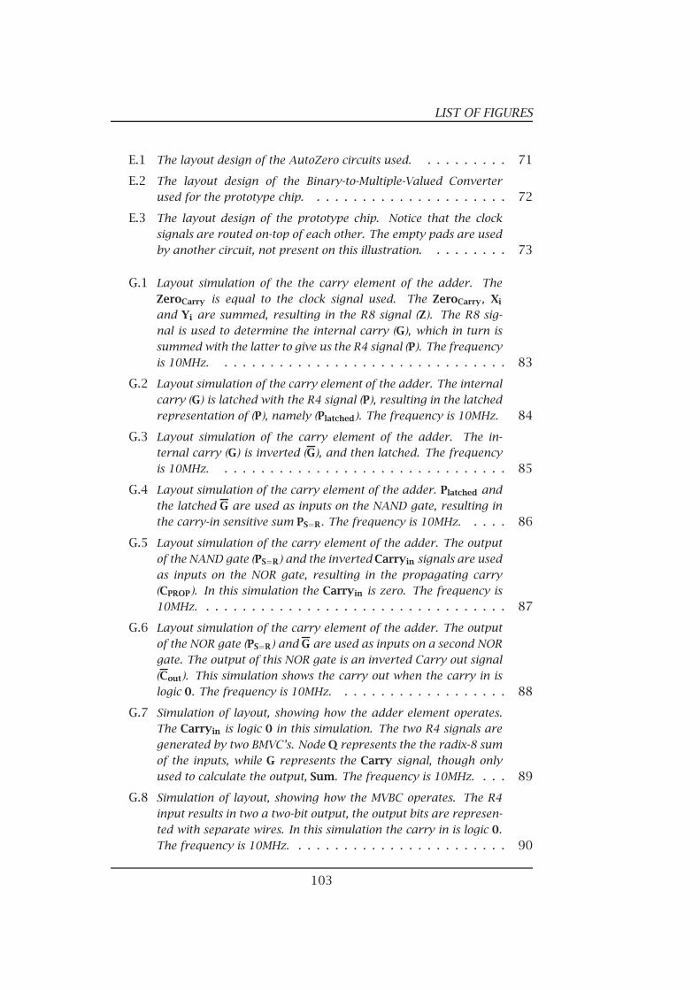
LIST OF FIGURES
E.1 The layout design of the AutoZero circuits used. . . . . . . . . . 71
E.2 The layout design of the Binary-to-Multiple-Valued Converterused for the prototype chip. . . . . . . . . . . . . . . . . . . . . . 72
E.3 The layout design of the prototype chip. Notice that the clocksignals are routed on-top of each other. The empty pads are usedby another circuit, not present on this illustration. . . . . . . . . 73
G.1 Layout simulation of the the carry element of the adder. TheZeroCarry is equal to the clock signal used. The ZeroCarry, Xi
and Yi are summed, resulting in the R8 signal (Z). The R8 sig-nal is used to determine the internal carry (G), which in turn issummed with the latter to give us the R4 signal (P). The frequencyis 10MHz. . . . . . . . . . . . . . . . . . . . . . . . . . . . . . . . 83
G.2 Layout simulation of the carry element of the adder. The internalcarry (G) is latched with the R4 signal (P), resulting in the latchedrepresentation of (P), namely (Platched). The frequency is 10MHz. 84
G.3 Layout simulation of the carry element of the adder. The in-ternal carry (G) is inverted (G), and then latched. The frequencyis 10MHz. . . . . . . . . . . . . . . . . . . . . . . . . . . . . . . . 85
G.4 Layout simulation of the carry element of the adder. Platched andthe latched G are used as inputs on the NAND gate, resulting inthe carry-in sensitive sum PS=R. The frequency is 10MHz. . . . . 86
G.5 Layout simulation of the carry element of the adder. The outputof the NAND gate (PS=R) and the inverted Carryin signals are usedas inputs on the NOR gate, resulting in the propagating carry(CPROP). In this simulation the Carryin is zero. The frequency is10MHz. . . . . . . . . . . . . . . . . . . . . . . . . . . . . . . . . . 87
G.6 Layout simulation of the carry element of the adder. The outputof the NOR gate (PS=R) and G are used as inputs on a second NORgate. The output of this NOR gate is an inverted Carry out signal(Cout). This simulation shows the carry out when the carry in islogic 0. The frequency is 10MHz. . . . . . . . . . . . . . . . . . . 88
G.7 Simulation of layout, showing how the adder element operates.The Carryin is logic 0 in this simulation. The two R4 signals aregenerated by two BMVC’s. Node Q represents the the radix-8 sumof the inputs, while G represents the Carry signal, though onlyused to calculate the output, Sum. The frequency is 10MHz. . . . 89
G.8 Simulation of layout, showing how the MVBC operates. The R4input results in two a two-bit output, the output bits are represen-ted with separate wires. In this simulation the carry in is logic 0.The frequency is 10MHz. . . . . . . . . . . . . . . . . . . . . . . . 90
103

LIST OF FIGURES
G.9 Simulation of layout, showing how the adder element operates.The Carryin is logic 1 in this simulation. The two R4 signals aregenerated by two MVBC’s. Node Q represents the the radix-8 sumof the inputs, while G represents the Carry signal, though onlyused to calculate the output, Sum. The frequency is 10MHz. . . . 91
G.10Simulation of layout, showing how the MVBC operates. The R4input results in two bit output, the output bits are representedwith separate wires. In this simulation the carry in is logic 1. Thefrequency is 10MHz. . . . . . . . . . . . . . . . . . . . . . . . . . 92
104

LIST OF TABLES
List of Tables
A.1 The propagation of the carry-signal through the Carry Element,with a Carry-in signal = 0 is illustrated. The essential Bits de-scribed in the text are bold. . . . . . . . . . . . . . . . . . . . . . 59
A.2 The propagation of the carry-signal through the Carry Elementis illustrated. This table shows the result of a Carry-In = 1. Theessential Bits described in the text are bold. . . . . . . . . . . . . 60
D.1 Instruments used for measurements. . . . . . . . . . . . . . . . . 67D.2 Pin List for single adder, test element. . . . . . . . . . . . . . . . 69D.3 Pin List for cascaded adders. . . . . . . . . . . . . . . . . . . . . . 70
105