Embed Size (px)
Citation preview
Carbon nanotube/indium tin oxide hybrid transparent conductive film:Effect of nanotube diameter
Mohammad Reza Golobostanfard a,n, Hossein Abdizadeh a,b, Saeed Mohammadi a,Mohammad Amin Baghchesara c
a School of Metallurgy and Materials Engineering, College of Engineering, University of Tehran, Tehran, Iranb Center of Excellence for High Performance Materials, University of Tehran, Tehran, Iranc Department of Metallurgy and Materials Engineering, Masjed Soleyman Branch, Islamic Azad University, Masjed Soleyman, Iran
a r t i c l e i n f o
Article history:Received 6 July 2014Received in revised form8 September 2014Accepted 25 September 2014
Keywords:Indium tin oxideSol–gelDip coatingCarbon nanotube diameterHybrid transparent conductiveOptoelectrical property
a b s t r a c t
Hybrid transparent conductive films (TCFs) based on indium tin oxide (ITO) and carbon nanotubes(CNTs) are prepared through a sol–gel dip coating method. The effect of CNT diameter on optoelectricalproperties of TCF is investigated. The surface roughness and grain size are decreased and the opticaltransmittance is increased with CNT diameter. The existence of bundles in smaller CNTs is the mainreason for lower transmittance in these samples. In terms of electrical resistivity, the large diameter CNTincorporated ITO film shows lower sheet resistance than bare ITO film at high enough film thicknesses.It seems that the large diameter CNT incorporation in ITO matrix can remarkably reduce the microcrackformation, especially at higher thicknesses, and act as nanobridges when microcracks are formed.Furthermore, the sensitivity of ITO film to thermal cycling is dramatically enhanced with these CNTs. Inaddition, the figure of merit of ITO film is considerably improved with large diameter CNT incorporation.
& 2014 Elsevier B.V. All rights reserved.
1. Introduction
Transparent conductive films (TCFs) are widely used in variousoptoelectronic devices such as liquid crystal displays, thin filmsolar cells, touch panels, e-papers, and flexible displays [1–4].So far different types of TCFs have been introduced, includingbinary oxides (indium tin oxide (ITO), flour tin oxide (FTO),aluminum zinc oxide (AZO)) [5], ternary oxides (Cd2SnO4,Zn2In2O5, and Zn2SnO4) [6], conducting polymers (poly(3,4-ethy-lene dioxythiophene/polystyrene sulfonate (PEDOT/PSS) and poly-aniline (PANI)) [7], and new generation materials (carbonnanotubes (CNTs), graphene, and metal grids) [8]. Among them,tin doped indium oxide (ITO) is widely used due to its hightransparency, low electrical resistivity, and proper chemical stabi-lity. However, the expensiveness and brittleness of ITO filmsstrongly limit their application [9–11].
The expensiveness of these films results from very high price ofindium raw material as well as high production cost of ultrahighvacuum deposition systems [12,13]. The production cost can bereduced by using chemical deposition methods such as spraypyrolysis and sol–gel. The sol–gel method with the advantages ofinexpensiveness, high yield, ability to form composite structure,
and non-vacuum apparatus seems to be a promising candidate forITO preparation with high performance per cost [14,15]. Thebrittleness of ITO films causes microcrack formation during filmdeposition, which strongly affects the charge transport propertiesand optical transmittance [16]. The microcrack formation can beentirely neutralized by incorporating second conductive toughphase in ITO matrix such as CNTs, graphene, conductive polymers,or metal grids. Although graphene sheets have very low resistivityand very high mobility (μ), they should be fully reduced fromgraphene oxide to show their appropriate electrical properties[17]. Also, the suitable dispersion of graphene in ITO sol and defectspreading in graphene structure after high temperature calcina-tion still remain as challenges in this composite [18]. The problemsfor conductive polymers are their high electrical sensitivity tohumidity, UV, and thermal exposure [19]. The major bottlenecksfor metal grids are their surface sensitivity to oxidation and highphoton scattering [20]. Outstanding chemical, optical, electrical,and mechanical properties of CNTs represent them as a promisingsubstitute for TCFs [21]. However, the relatively low visibletransparency of CNT films, low density of CNT films, and chargetransport barrier at the CNT/CNT junctions limit their applicationas TCF [22].
Although CNTs have much lower carrier concentration than ITOfilms (�1017/cm3 for CNT and 1020/cm3 for ITO), they showsubstantially higher μ [23]. Since the conductivity (σ) of a film isdirectly related to the number of charge carriers and μ, the σ can
Contents lists available at ScienceDirect
journal homepage: www.elsevier.com/locate/solmat
Solar Energy Materials & Solar Cells
http://dx.doi.org/10.1016/j.solmat.2014.09.0360927-0248/& 2014 Elsevier B.V. All rights reserved.
n Corresponding author. Tel.: þ98 9122300382; fax: þ98 21 88006076.E-mail address: [email protected] (M.R. Golobostanfard).
Solar Energy Materials & Solar Cells 132 (2015) 418–424
be tuned by either doping or using high mobility charge transportchannels. The figure of merit for TCF film, which can be describedby σ/α ratio (α is absorption coefficient), is dramatically reducedby increasing the number of charge carriers as a result of scatter-ing [24]. Therefore, enhancing the charge mobility would be amore efficient strategy for improving the σ of ITO film withoutaffecting the figure of merit. CNTs with high mobility may act astransport channels in ITO matrix without affecting the filmtransparency in visible region. Furthermore, they may reduce themicrocrack formation in ITO matrix and lead to higher σ.
Most composite TCFs are based on conductive polymers such asPEDOT:PSS with CNTs [25–27]. Making a composite based on ITOand CNT is rarely reported, (for example, ITO was deposited onCNT layer to make multilayer ITO/CNT film) [28]. However,incorporation of CNTs in ITO thin film has never been reported.Since the CNT diameter can entirely affect its chemical, thermal,and electrical properties [29–31], in this research, CNTs withdifferent diameters are incorporated in sol–gel synthesized ITOthin films and the effects of CNT diameter on optical and electricalproperties of ITO/CNT hybrid electrodes are investigated.
2. Experimental
2.1. Materials
Anhydrous indium chloride (InCl3, Alfa Aesar, 99.99%), tin chloride(SnCl2 �2 H2O, Merck, 98%), acetylacetone (AcAc, Merck, 99%), absoluteethanol (EtOH, Merck, 99%), sulfuric acid (H2SO4, Merck, 98%), andnitric acid (HNO3, Merck, 68%) were used as received without furtherpurification. SWCNT (outer diameter o2 nm, 95% purity, 60% single-wall, 350–400m2/g), MWCNT-10 (outer diameter o10 nm, 97%purity, 250–300 m2/g), and MWCNT-60 (outer diameter 40–60 nm,97% purity, 130–160m2/g) were purchased from Shenzen Nanotechport. Deionized water (DIW, 18.2 MΩ) was used in all experiments.
2.2. CNT functionalization
CNTs were subjected to ultrasonication in concentrated HNO3:H2SO4 (3:1 vol%) for 10 min. Then, the mixture was refluxed at80 1C for 1 h. Next, the mixture was diluted and washed with DIWby using centrifugation several times to ensure removal of anions.The product was dried at 60 1C and kept dry until use.
2.3. ITO/CNT sol preparation and film deposition
ITO sol preparation was previously reported [32]. Briefly,0.2 mol InCl3 was dissolved in AcAc and the resultant solutionwas refluxed at 85 1C for 1 h. Then, the required amount of SnCl2was dissolved in EtOH. The Sn/(InþSn) ratio was 6% in atomicratio. The InCl3 solution was added to the SnCl2 solution andrefluxed at 85 1C for another 1 h. For ITO/CNT sol, 0.02 g/L SWCNTwas added to SnCl2 solution and sonicated for 30 min. The othersteps were similar to those of ITO sol preparation. All the sols wereaged for 24 h before deposition. Various amounts of SWCNT, 0.01,0.02, and 0.04 g/L, were considered to investigate the effect of CNTcontent on optoeletrical properties of the composites. The sameamounts of MWCNT-10 and MWCNT-60 were also considered.
Before film deposition, the glass substrates were thoroughlycleaned ultrasonically in DIW and EtOH. Then, the prepared solswere deposited on substrates by means of the dip coating method.The withdrawal speed was 120 mm/min. Then, the films weredried at 350 1C for 10 min. The dip coating and drying processeswere repeated several times to reach the desired thickness. Finally,the films were annealed at 600 1C for 1 h.
2.4. Characterization
The surface functional groups of CNTs were investigated by aFourier-transformed infrared (FTIR) spectrophotometer, BrukerTENSOR27, in transmittance mode at 400–4000 cm�1 with KBras blank. Raman spectra were recorded using a BRUKER (SETERRA,spectral resolution o3 cm�1) micro-Raman spectrometerequipped with a confocal microscope. The excitation wavelengthwas the 785 nm line of an argon laser operating at the power of25 mW. The CNTs debundling and interfaces were studied bymeans of a high resolution transmission electron microscope(HRTEM), Philips CM30, 300 kV. The morphology and thicknessof the films were investigated by field emission scanning electronmicroscopy (FESEM), Hitachi S4160. The transmission spectra andoptical band gap in the UV–vis–NIR range were determined on aUV–vis spectrophotometer PG instrument, model T80þ . Theresistivity of the films was measured by a four-point probe methodKeithly model 196 Sys-DMM2 at room temperature.
3. Results and discussion
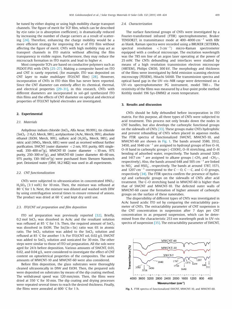
CNTs should be fully debundled before incorporation in ITOmatrix. For this purpose, all three types of CNTs were subjected toacid treatment. This process not only breaks down the nodes inCNT bundles, but also develops the carboxylic functional groupson the sidewalls of CNTs [33]. These groups make CNTs hydrophilicand prevent rebundling of CNTs when placed in aqueous media.The FTIR spectra of functionalized SWCNT, MWCNT-10, andMWCNT-60 are shown in Fig. 1. The bands around 3580, 3512,3450, and 1640 cm�1 are assigned to hydroxyl groups of free O–H,O–H band in carboxylic groups (–COOH), O–H stretching, and O–Hbending of adsorbed water, respectively. The bands around 3265and 1417 cm�1 are assigned to alkane groups (–CH3 and –CH2–,respectively). Also, the bands around 648 and 505 cm�1 are linkedto NO�
3 and HSO�4 , respectively. The bands at around 1787, 1571,
and 1207 cm�1 correspond to the CQO, CQC, and C–O groups,respectively [34]. The FTIR spectra confirm the presence of hydro-xyl and carboxylic groups on the sidewalls of CNTs after acidtreatment. The C–O stretching band in MWCNT-60 is higher thanthat of SWCNT and MWCNT-10. The defected outer walls ofMWCNT-60 cause the formation of higher amount of carboxylicgroups on the surface of these nanotubes.
The dispersibility of different types of CNTs was investigated inAcAc based acidic ITO sol by comparing the extractability para-meter of CNTs. The extractability parameter of CNT suspension isthe CNT concentration in suspension after 7 days per CNTconcentration in as prepared suspension, which can be deter-mined from the characteristic 253 nm wavelength peak in UV–visspectra of suspension [35]. The extractability parameter of SWCNT,
Fig. 1. FTIR spectra of functionalized SWCNT, MWCNT-10, and MWCNT-60.
M.R. Golobostanfard et al. / Solar Energy Materials & Solar Cells 132 (2015) 418–424 419
MWCNT-10, and MWCNT-60 is 32%, 19%, and 68%, respectively.This shows that the most stable dispersion in ITO sol could beobtained in MWCNT-60. The ITO sol is totally acidic with the pH ofless than 0.5. Although the defects of small diameter CNTs arelower than that of large diameter CNTs, the chemical stability ofthese CNTs is lower [36]. On the other hand, the tendency of smalldiameter CNTs to bundle is higher than that of large diameter CNTs[37]. The carboxylic groups on the sidewalls of CNTs can deproto-nate the surrounding media and result in stable dispersion ofCNTs. However, the deprotonation is limited in strong acidicmedia, which reduces the dispersibility of carboxylic functiona-lized CNTs in acidic media. Therefore, it seems that the highdispersibility of MWCNT-60 is mainly due to its higher surfacecarboxylic functional groups and their effective debundling duringthe acid treatment process. The lower defective sidewalls, whichallows lower attachment of carboxylic groups as well as highertendency to rebundle in SWCNT and MWCNT-10, cause lowerdispersibility in ITO sol for these nanotubes.
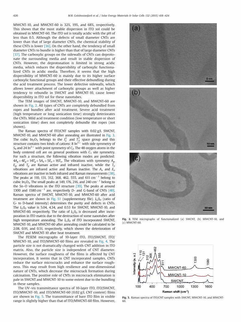
The TEM images of SWCNT, MWCNT-10, and MWCNT-60 areshown in Fig. 2. All types of CNTs are completely debundled fromropes and bundles after acid treatment. Severe acid treatment(high temperature or long sonication time) strongly deterioratesthe CNTs. Mild acid treatment condition (low temperature or shortsonication time) does not completely debundle the ropes (notshown).
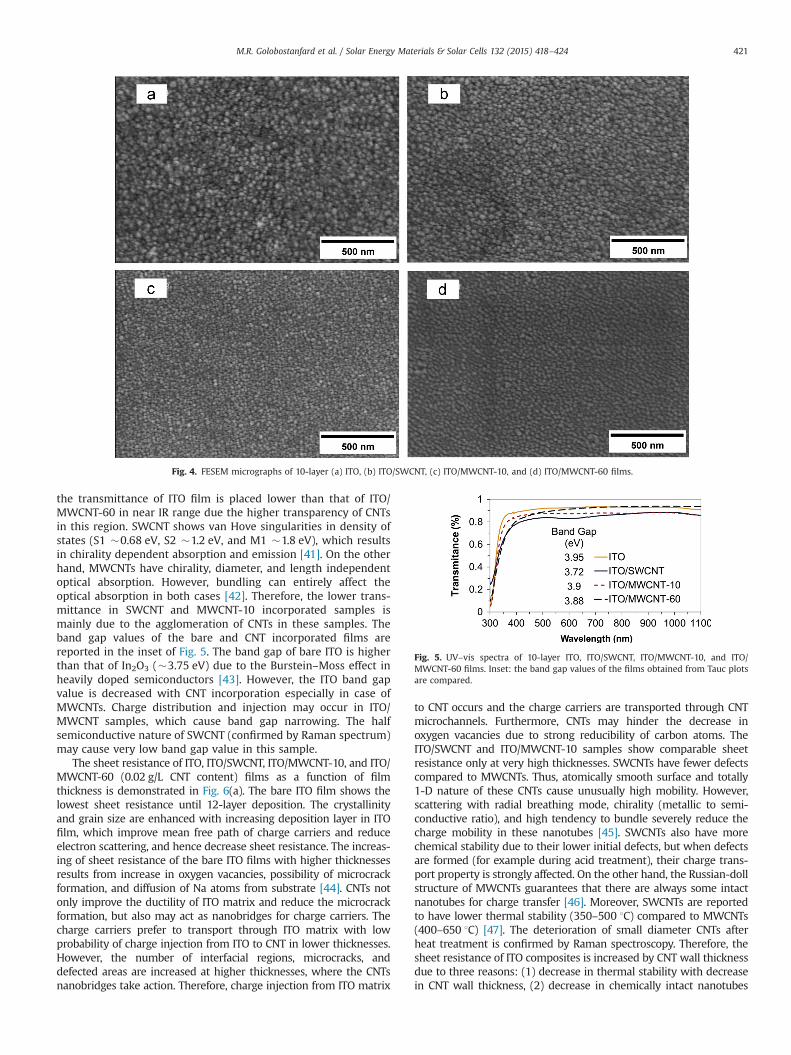
The Raman spectra of ITO/CNT samples with 0.02 g/L SWCNT,MWCNT-10, and MWCNT-60 after annealing are illustrated in Fig. 3.The cubic In2O3 belongs to the I3a and T7
h space group and thisstructure contains two kinds of cations: 8 In3þ with side symmetry ofS6 and 24 In3þ with point symmetry of C2. The 48 oxygen atoms in thebody centered cell are on general positions with C1 site symmetry.For such a structure, the following vibration modes are predicted:4Agþ4Egþ14Tgþ5Auþ5Euþ16Tu. The vibrations with symmetry Ag,Eg, and Tg are Raman active and infrared inactive, while the Tuvibrations are infrared active and Raman inactive. The Au and Euvibrations are inactive in both infrared and Ramanmeasurements [38].The peaks at 110, 131, 312, 368, 462, 555, and 611 cm�1 belong tocubic In2O3. The small peaks at 149, 176, 216, and 240 cm�1 belong tothe Sn–O vibrations in the ITO structure [39]. The peaks at around1300 and 1580 cm�1 are, respectively D- and G-band of CNTs [40].Raman spectra of SWCNT, MWCNT-10, and MWCNT-60 after acidtreatment are shown in Fig. S1 (supplementary file). IG/ID (ratio ofG- to D-band intensity) determines the purity and defects in CNTs.The IG/ID value is 5.04, 4.34, and 0.53 for SWCNT, MWCNT-10, andMWCNT-60, respectively. The ratio of IG/ID is decreased after incor-poration in ITO matrix due to the destruction of some nanotubes afterhigh temperature annealing. The IG/ID of ITO incorporated SWCNT,MWCNT-10, and MWCNT-60 after annealing could be calculated to be2.08, 0.91, and 0.51, respectively, which shows the deterioration ofSWCNT and MWCNT-10 after heat treatment.
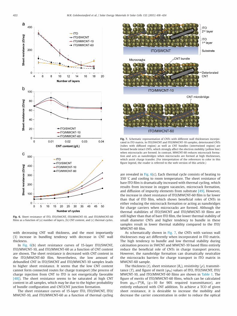
The FESEM micrographs of 10-layer ITO, ITO/SWCNT, ITO/MWCNT-10, and ITO/MWCNT-60 films are revealed in Fig. 4. Theparticle size is not dramatically changed with CNT addition in ITOmatrix. Also, the particle size is independent of CNT diameter.However, the surface roughness of the films is affected by CNTincorporation. It seems that in CNT incorporated samples, CNTsreduce the surface microcracks and enhance the surface rough-ness. This may result from high resilience and one-dimensionalnature of CNTs, which decrease the microcrack formation duringcalcination. The positive role of CNTs in microcrack elimination ispale in SWCNT and MWCNT-10 to some extent due to the bundlingin these samples.
The UV–vis transmittance spectra of 10-layer ITO, ITO/SWCNT,ITO/MWCNT-10, and ITO/MWCNT-60 (0.02 g/L CNT content) filmsare shown in Fig. 5. The transmittance of bare ITO film in visiblerange is slightly higher than that of ITO/MWCNT-60 film. However,
Fig. 2. TEM micrographs of functionalized (a) SWCNT, (b) MWCNT-10, and(c) MWCNT-60.
Fig. 3. Raman spectra of ITO/CNT samples with SWCNT, MWCNT-10, and MWCNT-60.
M.R. Golobostanfard et al. / Solar Energy Materials & Solar Cells 132 (2015) 418–424420
the transmittance of ITO film is placed lower than that of ITO/MWCNT-60 in near IR range due the higher transparency of CNTsin this region. SWCNT shows van Hove singularities in density ofstates (S1 �0.68 eV, S2 �1.2 eV, and M1 �1.8 eV), which resultsin chirality dependent absorption and emission [41]. On the otherhand, MWCNTs have chirality, diameter, and length independentoptical absorption. However, bundling can entirely affect theoptical absorption in both cases [42]. Therefore, the lower trans-mittance in SWCNT and MWCNT-10 incorporated samples ismainly due to the agglomeration of CNTs in these samples. Theband gap values of the bare and CNT incorporated films arereported in the inset of Fig. 5. The band gap of bare ITO is higherthan that of In2O3 (�3.75 eV) due to the Burstein–Moss effect inheavily doped semiconductors [43]. However, the ITO band gapvalue is decreased with CNT incorporation especially in case ofMWCNTs. Charge distribution and injection may occur in ITO/MWCNT samples, which cause band gap narrowing. The halfsemiconductive nature of SWCNT (confirmed by Raman spectrum)may cause very low band gap value in this sample.
The sheet resistance of ITO, ITO/SWCNT, ITO/MWCNT-10, and ITO/MWCNT-60 (0.02 g/L CNT content) films as a function of filmthickness is demonstrated in Fig. 6(a). The bare ITO film shows thelowest sheet resistance until 12-layer deposition. The crystallinityand grain size are enhanced with increasing deposition layer in ITOfilm, which improve mean free path of charge carriers and reduceelectron scattering, and hence decrease sheet resistance. The increas-ing of sheet resistance of the bare ITO films with higher thicknessesresults from increase in oxygen vacancies, possibility of microcrackformation, and diffusion of Na atoms from substrate [44]. CNTs notonly improve the ductility of ITO matrix and reduce the microcrackformation, but also may act as nanobridges for charge carriers. Thecharge carriers prefer to transport through ITO matrix with lowprobability of charge injection from ITO to CNT in lower thicknesses.However, the number of interfacial regions, microcracks, anddefected areas are increased at higher thicknesses, where the CNTsnanobridges take action. Therefore, charge injection from ITO matrix
to CNT occurs and the charge carriers are transported through CNTmicrochannels. Furthermore, CNTs may hinder the decrease inoxygen vacancies due to strong reducibility of carbon atoms. TheITO/SWCNT and ITO/MWCNT-10 samples show comparable sheetresistance only at very high thicknesses. SWCNTs have fewer defectscompared to MWCNTs. Thus, atomically smooth surface and totally1-D nature of these CNTs cause unusually high mobility. However,scattering with radial breathing mode, chirality (metallic to semi-conductive ratio), and high tendency to bundle severely reduce thecharge mobility in these nanotubes [45]. SWCNTs also have morechemical stability due to their lower initial defects, but when defectsare formed (for example during acid treatment), their charge trans-port property is strongly affected. On the other hand, the Russian-dollstructure of MWCNTs guarantees that there are always some intactnanotubes for charge transfer [46]. Moreover, SWCNTs are reportedto have lower thermal stability (350–500 1C) compared to MWCNTs(400–650 1C) [47]. The deterioration of small diameter CNTs afterheat treatment is confirmed by Raman spectroscopy. Therefore, thesheet resistance of ITO composites is increased by CNT wall thicknessdue to three reasons: (1) decrease in thermal stability with decreasein CNT wall thickness, (2) decrease in chemically intact nanotubes
Fig. 4. FESEM micrographs of 10-layer (a) ITO, (b) ITO/SWCNT, (c) ITO/MWCNT-10, and (d) ITO/MWCNT-60 films.
Fig. 5. UV–vis spectra of 10-layer ITO, ITO/SWCNT, ITO/MWCNT-10, and ITO/MWCNT-60 films. Inset: the band gap values of the films obtained from Tauc plotsare compared.
M.R. Golobostanfard et al. / Solar Energy Materials & Solar Cells 132 (2015) 418–424 421
with decreasing CNT wall thickness, and the most importantly(3) increase in bundling tendency with decrease in CNT wallthickness.
In Fig. 6(b) sheet resistance curves of 15-layer ITO/SWCNT,ITO/MWCNT-10, and ITO/MWCNT-60 as a function of CNT contentare shown. The sheet resistance is decreased with CNT content inthe ITO/MWCNT-60 film. Nevertheless, the low amount ofdebundled CNT in ITO/SWCNT and ITO/MWCNT-10 samples leadsto higher sheet resistance. It seems that the low CNT contentcannot form connected routes for charge transport (the process ofcharge injection from CNT to ITO is not energetically favorable[48]). The sheet resistance seems to be saturated at high CNTcontent in all samples, which may be due to the higher probabilityof bundle configuration and CNT/CNT junction formation.
The sheet resistance curves of 15-layer ITO, ITO/SWCNT, ITO/MWCNT-10, and ITO/MWCNT-60 as a function of thermal cycling
are revealed in Fig. 6(c). Each thermal cycle consists of heating to350 1C and cooling to room temperature. The sheet resistance ofbare ITO film is dramatically increased with thermal cycling, whichresults from increase in oxygen vacancies, microcrack formation,and diffusion of impurity elements from substrate [49]. However,the increase in sheet resistance of ITO/MWCNT-60 film is far lowerthan that of ITO film, which shows beneficial roles of CNTs ineither reducing the microcrack formation or acting as nanobridgesfor charge carriers when microcracks are formed. Although thethermal stabilities of ITO/SWCNT and ITO/MWCNT-10 films arestill higher than that of bare ITO film, the lower thermal stability ofsmall diameter CNTs and higher tendency to bundle in thesesamples result in lower thermal stability compared to the ITO/MWCNT-60 film.
As schematically shown in Fig. 7, the CNTs with various wallthicknesses may act differently when incorporated in ITO matrix.The high tendency to bundle and low thermal stability duringcalcination process in SWCNT and MWCNT-10 based films entirelyreduce the beneficial role of CNTs in charge transport process.However, the nanobridge formation can dramatically neutralizethe microcracks barriers for charge transport in ITO matrix inMWCNT-60 sample.
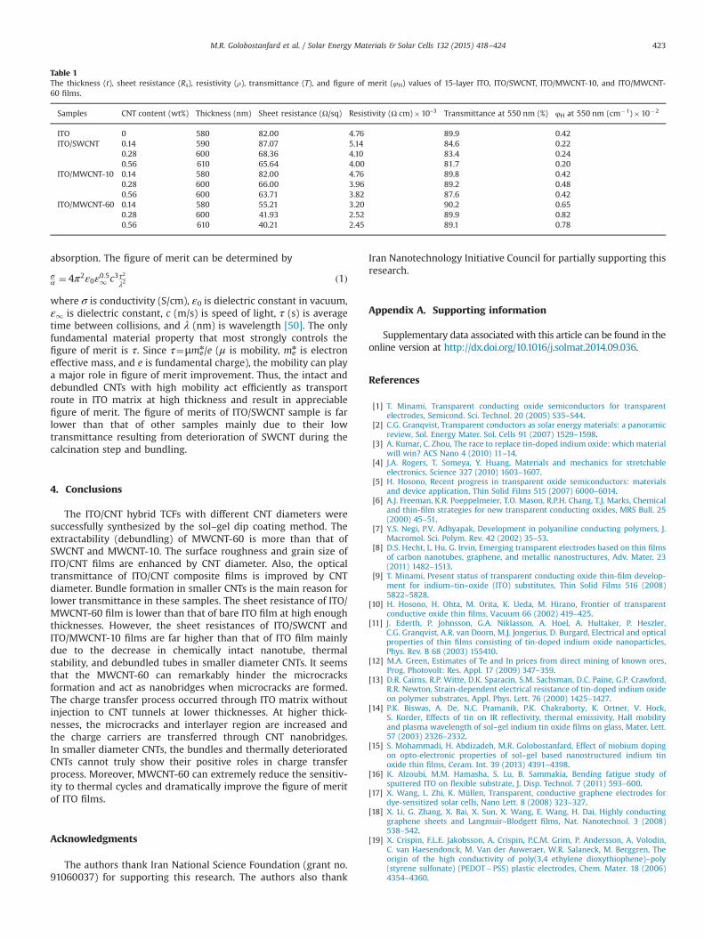
The thickness (t), sheet resistance (Rs), resistivity (ρ), transmit-tance (T), and figure of merit (φH) values of ITO, ITO/SWCNT, ITO/MWCNT-10, and ITO/MWCNT-60 films are shown in Table 1. Thefigure of merits of ITO/MWCNT-60 films, which can be calculatedfrom φH¼Tq/Rs (q¼10 for 90% required transmittance), areentirely enhanced with CNT addition. To achieve a TCO of givensheet resistance, it is desirable to increase the mobility anddecrease the carrier concentration in order to reduce the optical
Fig. 6. Sheet resistance of ITO, ITO/SWCNT, ITO/MWCNT-10, and ITO/MWCNT-60films as a function of (a) number of layers, (b) CNT content, and (c) thermal cycles.
Fig. 7. Schematic representation of CNTs with different wall thicknesses incorpo-rated in ITO matrix. In ITO/SWCNT and ITO/MWCNT-10 samples, deteriorated CNTs(tubes with diffused region) as well as CNT bundles (intertwined region) areformed beside intact CNTs, which strongly affect the electron mobility (yellow line)when microcracks are formed. In contrast, MWCNT-60 reduces microcrack forma-tion and acts as nanobridges when microcracks are formed at high thicknesses,which assist charge transfer. (For interpretation of the references to color in thisfigure legend, the reader is referred to the web version of this article.)
M.R. Golobostanfard et al. / Solar Energy Materials & Solar Cells 132 (2015) 418–424422
absorption. The figure of merit can be determined by
σα ¼ 4π2ε0ε0:51 c3τ
2
λ2ð1Þ
where σ is conductivity (S/cm), ε0 is dielectric constant in vacuum,ε1 is dielectric constant, c (m/s) is speed of light, τ (s) is averagetime between collisions, and λ (nm) is wavelength [50]. The onlyfundamental material property that most strongly controls thefigure of merit is τ. Since τ¼μme
n/e (μ is mobility, men is electron
effective mass, and e is fundamental charge), the mobility can playa major role in figure of merit improvement. Thus, the intact anddebundled CNTs with high mobility act efficiently as transportroute in ITO matrix at high thickness and result in appreciablefigure of merit. The figure of merits of ITO/SWCNT sample is farlower than that of other samples mainly due to their lowtransmittance resulting from deterioration of SWCNT during thecalcination step and bundling.
4. Conclusions
The ITO/CNT hybrid TCFs with different CNT diameters weresuccessfully synthesized by the sol–gel dip coating method. Theextractability (debundling) of MWCNT-60 is more than that ofSWCNT and MWCNT-10. The surface roughness and grain size ofITO/CNT films are enhanced by CNT diameter. Also, the opticaltransmittance of ITO/CNT composite films is improved by CNTdiameter. Bundle formation in smaller CNTs is the main reason forlower transmittance in these samples. The sheet resistance of ITO/MWCNT-60 film is lower than that of bare ITO film at high enoughthicknesses. However, the sheet resistances of ITO/SWCNT andITO/MWCNT-10 films are far higher than that of ITO film mainlydue to the decrease in chemically intact nanotube, thermalstability, and debundled tubes in smaller diameter CNTs. It seemsthat the MWCNT-60 can remarkably hinder the microcracksformation and act as nanobridges when microcracks are formed.The charge transfer process occurred through ITO matrix withoutinjection to CNT tunnels at lower thicknesses. At higher thick-nesses, the microcracks and interlayer region are increased andthe charge carriers are transferred through CNT nanobridges.In smaller diameter CNTs, the bundles and thermally deterioratedCNTs cannot truly show their positive roles in charge transferprocess. Moreover, MWCNT-60 can extremely reduce the sensitiv-ity to thermal cycles and dramatically improve the figure of meritof ITO films.
Acknowledgments
The authors thank Iran National Science Foundation (grant no.91060037) for supporting this research. The authors also thank
Iran Nanotechnology Initiative Council for partially supporting thisresearch.
Appendix A. Supporting information
Supplementary data associated with this article can be found in theonline version at http://dx.doi.org/10.1016/j.solmat.2014.09.036.
References
[1] T. Minami, Transparent conducting oxide semiconductors for transparentelectrodes, Semicond. Sci. Technol. 20 (2005) S35–S44.
[2] C.G. Granqvist, Transparent conductors as solar energy materials: a panoramicreview, Sol. Energy Mater. Sol. Cells 91 (2007) 1529–1598.
[3] A. Kumar, C. Zhou, The race to replace tin-doped indium oxide: which materialwill win? ACS Nano 4 (2010) 11–14.
[4] J.A. Rogers, T. Someya, Y. Huang, Materials and mechanics for stretchableelectronics, Science 327 (2010) 1603–1607.
[5] H. Hosono, Recent progress in transparent oxide semiconductors: materialsand device application, Thin Solid Films 515 (2007) 6000–6014.
[6] A.J. Freeman, K.R. Poeppelmeier, T.O. Mason, R.P.H. Chang, T.J. Marks, Chemicaland thin-film strategies for new transparent conducting oxides, MRS Bull. 25(2000) 45–51.
[7] Y.S. Negi, P.V. Adhyapak, Development in polyaniline conducting polymers, J.Macromol. Sci. Polym. Rev. 42 (2002) 35–53.
[8] D.S. Hecht, L. Hu, G. Irvin, Emerging transparent electrodes based on thin filmsof carbon nanotubes, graphene, and metallic nanostructures, Adv. Mater. 23(2011) 1482–1513.
[9] T. Minami, Present status of transparent conducting oxide thin-film develop-ment for indium–tin–oxide (ITO) substitutes, Thin Solid Films 516 (2008)5822–5828.
[10] H. Hosono, H. Ohta, M. Orita, K. Ueda, M. Hirano, Frontier of transparentconductive oxide thin films, Vacuum 66 (2002) 419–425.
[11] J. Ederth, P. Johnsson, G.A. Niklasson, A. Hoel, A. Hultaker, P. Heszler,C.G. Granqvist, A.R. van Doorn, M.J. Jongerius, D. Burgard, Electrical and opticalproperties of thin films consisting of tin-doped indium oxide nanoparticles,Phys. Rev. B 68 (2003) 155410.
[12] M.A. Green, Estimates of Te and In prices from direct mining of known ores,Prog. Photovolt: Res. Appl. 17 (2009) 347–359.
[13] D.R. Cairns, R.P. Witte, D.K. Sparacin, S.M. Sachsman, D.C. Paine, G.P. Crawford,R.R. Newton, Strain-dependent electrical resistance of tin-doped indium oxideon polymer substrates, Appl. Phys. Lett. 76 (2000) 1425–1427.
[14] P.K. Biswas, A. De, N.C. Pramanik, P.K. Chakraborty, K. Ortner, V. Hock,S. Korder, Effects of tin on IR reflectivity, thermal emissivity, Hall mobilityand plasma wavelength of sol–gel indium tin oxide films on glass, Mater. Lett.57 (2003) 2326–2332.
[15] S. Mohammadi, H. Abdizadeh, M.R. Golobostanfard, Effect of niobium dopingon opto-electronic properties of sol–gel based nanostructured indium tinoxide thin films, Ceram. Int. 39 (2013) 4391–4398.
[16] K. Alzoubi, M.M. Hamasha, S. Lu, B. Sammakia, Bending fatigue study ofsputtered ITO on flexible substrate, J. Disp. Technol. 7 (2011) 593–600.
[17] X. Wang, L. Zhi, K. Müllen, Transparent, conductive graphene electrodes fordye-sensitized solar cells, Nano Lett. 8 (2008) 323–327.
[18] X. Li, G. Zhang, X. Bai, X. Sun, X. Wang, E. Wang, H. Dai, Highly conductinggraphene sheets and Langmuir–Blodgett films, Nat. Nanotechnol. 3 (2008)538–542.
[19] X. Crispin, F.L.E. Jakobsson, A. Crispin, P.C.M. Grim, P. Andersson, A. Volodin,C. van Haesendonck, M. Van der Auweraer, W.R. Salaneck, M. Berggren, Theorigin of the high conductivity of poly(3,4 ethylene dioxythiophene)–poly(styrene sulfonate) (PEDOT�PSS) plastic electrodes, Chem. Mater. 18 (2006)4354–4360.
Table 1The thickness (t), sheet resistance (Rs), resistivity (ρ), transmittance (T), and figure of merit (φH) values of 15-layer ITO, ITO/SWCNT, ITO/MWCNT-10, and ITO/MWCNT-60 films.
Samples CNT content (wt%) Thickness (nm) Sheet resistance (Ω/sq) Resistivity (Ω cm)�10–3 Transmittance at 550 nm (%) φH at 550 nm (cm�1)�10�2
ITO 0 580 82.00 4.76 89.9 0.42ITO/SWCNT 0.14 590 87.07 5.14 84.6 0.22
0.28 600 68.36 4.10 83.4 0.240.56 610 65.64 4.00 81.7 0.20
ITO/MWCNT-10 0.14 580 82.00 4.76 89.8 0.420.28 600 66.00 3.96 89.2 0.480.56 600 63.71 3.82 87.6 0.42
ITO/MWCNT-60 0.14 580 55.21 3.20 90.2 0.650.28 600 41.93 2.52 89.9 0.820.56 610 40.21 2.45 89.1 0.78
M.R. Golobostanfard et al. / Solar Energy Materials & Solar Cells 132 (2015) 418–424 423
[20] H. Wu, L. Hu, M.W. Rowell, D. Kong, J.J. Cha, J.R. McDonough, J. Zhu, Y. Yang,M.D. McGehee, Y. Cui, Electrospun metal nanofiber webs as high-performancetransparent electrode, Nano Lett. 10 (2010) 4242–4248.
[21] Z. Wu, Z. Chen, X. Du, J.M. Logan, J. Sippel, M. Nikolou, K. Kamaras, J.R. Reynolds, D.B. Tanner, A.F. Hebard, A.G. Rinzler, Transparent, conductivecarbon nanotube films, Science 305 (2004) 1273–1276.
[22] Z. Li, H.R. Kandel, E. Dervishi, V. Saini, Y. Xu, A.R. Biris, D. Lupu, G.J. Salamo,A.S. Biris, Comparative study on different carbon nanotube materials in termsof transparent conductive coatings, Langmuir 24 (2008) 2655–2662.
[23] L. Hu, D.S. Hecht, G. Grüner, Infrared transparent carbon nanotube thin films,Appl. Phys. Lett. 94 (2009) 081103.
[24] K. Ellmer, Past achievements and future challenges in the development ofoptically transparent electrodes, Nat. Photonics 6 (2012) 809–817.
[25] B. Fan, X. Mei, K. Sun, J. Ouyang, Conducting polymer/carbon nanotubecomposite as counter electrode of dye-sensitized solar cells, Appl. Phys. Lett.93 (2008) 143103.
[26] J. Li, J.C. Liu, C.J. Gao, On the mechanism of conductivity enhancement inPEDOT/PSS film doped with multi-walled carbon nanotubes, J. Polym. Res. 17(2010) 713–718.
[27] D. Antiohos, G. Folkes, P. Sherrell, S. Ashraf, G.G. Wallace, P. Aitchison,A.T. Harris, J. Chen, A.I. Minett, Compositional effects of PEDOT–PSS/singlewalled carbon nanotube films on supercapacitor device performance, J. Mater.Chem. 21 (2011) 15987–15994.
[28] A. Capasso, L. Salamandra, A. Chou, A. Di Carlo, N. Motta, Multi-wall carbonnanotube coating of fluorine-doped tin oxide as an electrode surface modifierfor polymer solar cells, Sol. Energy Mater. Sol. Cells 122 (2014) 297–302.
[29] D. Ostling, D. Tomanek, A. Rosen, Electronic structure of single-wall, multiwall,and filled carbon nanotubes, Phys. Rev. B 55 (1997) 13980–13988.
[30] D. Jariwala, V.K. Sangwan, L.J. Lauhon, T.J. Marks, M.C. Hersam, Carbonnanomaterials for electronics, optoelectronics, photovoltaics, and sensing,Chem. Soc. Rev. 42 (2013) 2824–2860.
[31] L. Dai, D.W. Chang, J.B. Baek, W. Lu, Carbon nanomaterials for advanced energyconversion and storage, Small 8 (2012) 1130–1166.
[32] S. Mohammadi, H. Abdizadeh, M.R. Golobostanfard, Opto-electronic proper-ties of molybdenum doped indium tin oxide nanostructured thin filmsprepared via sol–gel spin coating, Ceram. Int. 39 (2013) 6953–6961.
[33] D. Tasis, N. Tagmatarchis, A. Bianco, M. Prato, Chemistry of carbon nanotubes,Chem. Rev. 106 (2006) 1105–1136.
[34] A.G. Osorio, I.C.L. Silveira, V.L. Bueno, C.P. Bergmann, H2SO4/HNO3/HCl-functionalization and its effect on dispersion of carbon nanotubes in aqueousmedia, Appl. Surf. Sci. 255 (2008) 2485–2489.
[35] R. Rastogi, R. Kaushal, S.K. Tripathi, A.L. Sharma, I. Kaur, L.M. Bharadwaj,Comparative study of carbon nanotube dispersion using surfactants, J. ColloidInterface Sci. 328 (2008) 421–428.
[36] S.B. Sinnott, R. Andrews, Carbon nanotubes: synthesis, properties, andapplications, Crit. Rev. Solid State Mater. Sci. 26 (2001) 145–249.
[37] H. Wang, Dispersing carbon nanotubes using surfactants, Curr. Opin. ColloidInterface Sci. 14 (2009) 364–371.
[38] C.Y. Wang, Y. Dai, J. Pezoldt, B. Lu, T. Kups, V. Cimalla, O. Ambacher, Phasestabilization and phonon properties of single crystalline rhombohedralindium oxide, Cryst. Growth Des. 8 (2008) 1257–1260.
[39] O.M. Berengue, A.D. Rodrigues, C.J. Dalmaschio, A.J.C. Lanfredi, E.R. Leite,A.J. Chiquito, Structural characterization of indium oxide nanostructures: aRaman analysis, J. Phys. D: Appl. Phys. 43 (2010) 045401.
[40] M.S. Dresselhaus, G. Dresselhaus, R. Saito, A. Jorio, Raman spectroscopy ofcarbon nanotubes, Phys. Rep. 409 (2005) 47–99.
[41] H. Kataura, Y. Kumazawa, Y. Maniwa, I. Umezu, S. Suzuki, Y. Ohtsuka, Y. Achiba,Optical properties of single-wall carbon nanotubes, Synth. Met. 103 (1999)2555–2558.
[42] L. Hu, D.S. Hecht, G. Gruner, Carbon nanotube thin films: fabrication, proper-ties, and applications, Chem. Rev. 110 (2010) 5790–5844.
[43] O.N. Mryasov, A.J. Freeman, Electronic band structure of indium tin oxide andcriteria for transparent conducting behavior, Phys. Rev. B 64 (2001) 233111.
[44] M. Gross, A. Winnacker, P.J. Wellmann, Electrical, optical and morphologicalproperties of nanoparticle indium–tin–oxide layers, Thin Solid Films 515(2007) 8567–8572.
[45] J.C. Charlier, Defects in carbon nanotubes, Acc. Chem. Res. 35 (2002)1063–1069.
[46] M.R. Golobostanfard, H. Abdizadeh, Influence of carbon nanotube wall thick-ness on performance of dye sensitized solar cell with hierarchical porousphotoanode, Micropor. Mesopor. Mater. 191 (2014) 74–81.
[47] J.H. Lehman, M. Terrones, E. Mansfield, K.E. Hurst, V. Meunier, Evaluating thecharacteristics of multiwall carbon nanotubes, Carbon 49 (2011) 2581–2602.
[48] P.D.C. King, T.D. Veal, Conductivity in transparent oxide semiconductors, J.Phys.: Condens. Matter 23 (2011) 334214.
[49] M.M. Hamasha, T. Dhakal, K. Alzoubi, S. Albahri, A. Qasaimeh, S. Lu,C.R. Westgate, Stability of ITO thin film on flexible substrate under thermalaging and thermal cycling conditions, J. Disp. Technol. 8 (2012) 385–390.
[50] A. Luque, S. Hegedus, Handbook of Photovoltaic Science and Engineering,second edition, Wiley, New York, 2011.
M.R. Golobostanfard et al. / Solar Energy Materials & Solar Cells 132 (2015) 418–424424