Embed Size (px)
Citation preview
111111111111111111111111111111111111111111111111111111111111111111111111
w v z
V) z cc
(12) United States Patent Ruoff et al.
(54) CERAMIC COMPOSITE THIN FILMS
(75) Inventors: Rodney S. Ruoff, Skokie, IL (US); Sasha Stankovich, Spartanburg, SC (US); Dmitriy A. Dikin, Skokie, IL (US); SonBinh T. Nguyen, Evanston, IL (US)
(73) Assignee: Northwestern University, Evanston, IL (US)
(*) Notice: Subject to any disclaimer, the term of this patent is extended or adjusted under 35 U.S.C. 154(b) by 712 days.
(21) Appl. No.: 12/152,284
(22) Filed: May 13, 2008
(65) Prior Publication Data
US 2010/0323178 Al Dec. 23, 2010
Related U.S. Application Data
(60) Provisional application No. 60/930,102, filed on May 14, 2007.
(51) Int. Cl. B05D 3102 (2006.01)
(52) U.S. Cl. USPC ....................................................... 427/376.2
(58) Field of Classification Search USPC ....................................................... 427/376.2 See application file for complete search history.
(56) References Cited
U.S. PATENT DOCUMENTS
5,446,339 A * 8/1995 Kinoshita et al .............. 313/478 2003/0187124 Al * 10/2003 Hirata et al . .................. 524/496 2006/0102562 Al 5/2006 Cannon et al ................. 210/681
W v
0
0, oc
96
9%
94 11°/
400 600 800 1000 WAVE LENGTH (nm)
(lo) Patent No.: US 8,574,681 B2 (45) Date of Patent: Nov. 5, 2013
2006/0202105 Al 9/2006 Krames et al .............. 250/208.1 2007/0092432 Al 4/2007 Prud'Homme et al. ...... 423/448 2008/0048152 Al * 2/2008 Jang et al . ................. 252/378 R
OTHER PUBLICATIONS
Watcharotone et al "Graphene-based Silica Composite Thin Films", 2007 APS March Meeting Mar. 8, 2007.* Nicholas A. Kotov, et al., Ultrathin Graphite Oxide-Polyelectrolyte Composites Prepared by Self-Assembly: Transition Between Con-ductive and Non-Conductive States, Advanced Materials, 1996, 8, No. 8, pp. 637-641. Kuanping Gong, et al., Sol-Gel-Derived Ceramic—Carbon Nanotube Nanocomposite Electrodes: Tunable Electrode Demen-sion and Potential Electrochemical Applications, Analytical Chem-istry, 2004, 76, pp. 6500-6505. Michael W. Rowell, et al., Organic solar cells with carbon nanotube network electrodes, Applied Physics Letters, 2006, 88, pp. 233506(1-3).
(Continued)
Primary Examiner Nathan Empie (74) Attorney, Agent, or Firm Klintworth & Rozenblat IP LLC
(57) ABSTRACT
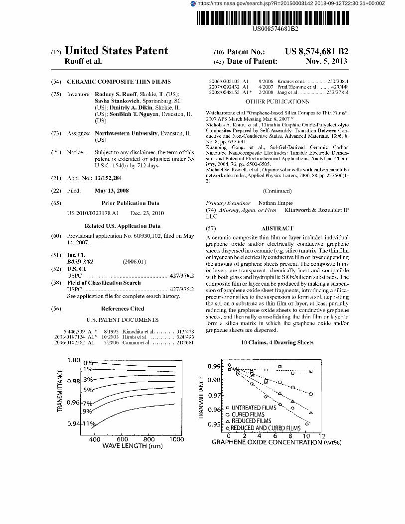
A ceramic composite thin film or layer includes individual graphene oxide and/or electrically conductive graphene sheets dispersed in a ceramic (e.g. silica) matrix. The thin film or layer can be electrically conductive film or layer depending the amount of graphene sheets present. The composite films or layers are transparent, chemically inert and compatible with both glass and hydrophilic SiOx/silicon substrates. The composite film or layer can be produced by making a suspen-sion of graphene oxide sheet fragments, introducing a silica-precursor or silica to the suspension to form a sol, depositing the sol on a substrate as thin film or layer, at least partially reducing the graphene oxide sheets to conductive graphene sheets, and thermally consolidating the thin film or layer to form a silica matrix in which the graphene oxide and/or graphene sheets are dispersed.
10 Claims, 4 Drawing Sheets
0.99 Q _ ❑ o ----0------------ ❑ - ----- - 0
0.98 ,~ • . ~
• o
0.97
0.96 ° UNTREATED FILMS a CURED FILMS ° ° REDUCED FILMS
0.95 o REDUCED AND CURED FILMS o 0 2 4 6 8 10 12
GRAPHENE OXIDE CONCENTRATION (wt%)
https://ntrs.nasa.gov/search.jsp?R=20150003142 2018-09-12T22:30:31+00:00Z
US 8,574,681 B2 Page 2
(56) References Cited
OTHER PUBLICATIONS
Pinggui Liu, et al., Synthesis of polyaniline-intercalated graphite oxide by an in situ oxidative polymerization reaction, Carbon, 1999, 37, pp. 701-711. Sasha Stankovich, et al., Synthesis and exfoliation of isocyanate-treated graphene oxide nanoplatelets, Carbon, 2006, pp. 3342-3347. Nina L Kovtyukhova, et al., Layer-by-Layer Assembly of Ultrathin Composite Films from Micron-Sized Graphite Oxide Sheets and Polycations, Chem. Mater., 1999, 11, pp. 771-778. O. Lev, et al., Sol-Gel Materials in Electrochemistry, Chem. Mater., 1997, 9, pp. 2354-2375. Hany Aziz, et al., Degradation Phenomena in Small-Molecule Organic Light-Emitting Devices, Chem. Mater., 2004, 16, pp. 4522-4532. Virginie Romeas, et al., Testing the Efficacy and the Potential Effect on Indoor Air Quality of a Transparent Self-Cleaning Ti0 2 -Coated Glass through the Degredation of a Fluoranthene Layer, Ind. Eng. Chem. Res., 1999, 38, pp. 3878-3885. G. Evmenenko, et al., Specular x-ray reflectivity study of ordering in self-assembled organic and hybrid organic-inorganic electro-optic multilayer films, J. Chem. Phys., 2001, 115, pp. 6722-6727. Toshiro Maryama and Kenji Tabata, Indium-Tin Oxide Thin Films Prepared by Chemical Vapor Deposition from Metal Acetates, Japa-nese Journal of Applied Physics, 1990, vol. 29, No. 2, pp. L 355-L 357. Sasha Stankovich, et al., Stable aqueous dispersions of graphitic nanoplatelets via the reduction of exfoliated graphite oxide in the presence of poly(sodium 4-styrenesulfonate), Journal of Materials Chemistry, 2006, 16, pp. 155-158. D. Shimono, et al., Preparation of transparent and conductive ZnO films using a chemical solution deposition process, Journal of Ceramic Processing Research, 2001, vol. 2. pp. 184-188. J.F. Chang, et al., Studying of transparent conductive ZnO: Al thin films by RF reactive magnetron sputtering, Journal of Crystal Growth, 2000, 211, pp. 93-97. Changshu Xiang, et al., Electrical properties of multiwalled carbon nanotube reinforced fused silica composites, Journal ofNanoscience and Nanotechnology, 2006, 6(12), pp. 3835-3841. Toshi Tsuchiya, et al., Preparation and properties oftransparent con-ductive thin films by the sol-gel process, Journal of Non-Crystalline Solids, 1994, 178, pp. 327-332. Masashi Ohyama, et al., Sol-Gel Preparation of Transparent and Conductive Aluminum-Doped Zinc Oxide Films with Highly Pref-erential Crystal Orientation, J. Am. Ceram. Soc., 1998, 81(6), pp. 1622-1632. William S. Hummers, Jr. and Richard E. Offeman, Preparation of Graphitic Oxide, Journal of the American Chemical Society, 1958, 80, p. 1339.
Changshu Xiang, et al., Fabrication and dielectric properties of CNTs/Si02 composites, Key Engineering Materials, 2005, pp. 280-283. Abstract. Thierry Cassagneau, et al., Preparation and Characterization of Ultrathin Films Layer-by-Layer Self-Assembled from Graphite Oxide Nanolatelets and Polymers, Langmuir, 2000, 16, pp. 7318-7324. Athanasios B. Bourlinos, et al., Graphite Oxide: Chemical Reduction to Graphite and Surface Modification with Primary Aliphatic Amines and Amino Acids, Langmuir, 2003, 19, pp. 6050-6055. E. Terzini, et al., Properties of ITO thin films deposited by RF magnetron sputtering at elevated substrate temperature, Materials Science & Engineering, B Solid-State Materials for Avanced Technolgy, 2000, pp. 110-114. Sasha Stankovich, et al., Graphene-based composite materials, Nature, 2006, vol. 442, pp. 282-286. J. Zhang, et al., Sol-gel preparation of poly(ethylene glycol) doped indium tin oxide thin films for sensing applications, Optical Materi-als, 2004, 26(1), pp. 47-55. Joseph G. Smith, Jr., et al., Carbon nanotube-conductive additive-space durable polymer nanocomposite films for electrostatic charge dissipation, Polymer, 2004, 45, pp. 6133-6142. Kent A. Watson, et al., Transparent, flexible, conductive carbon nanotube coatings for electrostatic charge mitigation, Polymer, 2005, 46, pp. 2076-2085. S.M. Rozati and T. Ganj, Transparent conductive Sn-doped indium oxide thin films deposited by spray pyrolysis technique, Renewable Energy, 2004, 29, pp. 1671-1676. Kunjal Parikh, et al., Flexible vapour sensors using single walled carbon nanotubes, Sensors and Actuators, B Chemical, 2006, 113, pp. 55-63. Qiang Wei, et al., Direct patterning ITO transparent conductive coat-ings, Solar Energy Materials & Solar Cells, 2001, 68, pp. 383-390. Yong Gan, et al., Transparent conductive indium tin oxide film fab-ricated by dip-coating technique from colloid precursor, Surface & Coatings Technology, 2006, 201, pp. 25-29. Seon-Soon Kim, et al., Transparent conductive ITO thin films through the sol-gel process using metal salts, Thin Solid Films, 1999, 347, pp. 155-160. C. Beneking, et al., Recent developments of silicon thin film solar cells on glass substrates, Thin Solid Films, 1999, 351, pp. 241-246. Kunisuke Maki, et al., Fabrication of thin films of ITO by aerosol CVD, Thin Solid Films, 2003, 445, pp. 224-228. Suzhu Yu, et al., Effect of processing temperature on the properties of sol-gel-derived mesoporous silica films, Thin Solid Films, 2004, 462-463, pp. 306-310. J.J. Finley, Heat treatment and bending of low-E glass, Thin Solid Films, 1999, 351, pp. 264-273.
* cited by examiner
U.S. Patent Nov. 5, 2013 Sheet 1 of 4 US 8,574,681 B2
FIG.
FIG. 1 b FG*
U.S. Patent Nov. 5, 2013 Sheet 2 of 4 US 8 ,574,681 B2
F I G. 2a
&
FIG. 2i '6,v.
2
~ j
FIG. 2
} -2
f~ 1~
..X
-----BEFORE CURING AFTER CURING
6 .
1 4
12
tsr :
0 Y
S
D 6
Gf`+f` PH£,..f'k;,:. OXIDE CON5„., 'O F2f`4TfON
0 V
Vnoo FIG. 3b
U.S. Patent Nov. 5, 2013 Sheet 3 of 4 US 8,574,681 B2
Q N 215 280 285 290 295 ry N J V in s n
FIG. 3C
CURED 11 °l0
ku%O
o ii v
CURED 0% 275 280 285 290 295
V
RIED 0°10 FIG. 3d
0 200 400 600 80010001200 BINDING ENERGY (eV)
FIG. 3a
0 V
00
11 VV
O
275 280 285 290 295
FIG.6
0
a 0
a
1
E
0.1
0.01 D
0 1 E-3
0.9!
v 0.9"
0.9
d 0.91 cc r
0.9;
U.S. Patent Nov. 5, 2013 Sheet 4 of 4 US 8,574,681 B2
FIG.4
FIG. 5a
0.95 0 2 4 6 8 10 12
GRAPHEME OXIDE CONCENTRATION (wt%)
1.00 0°l
v 0.98 3°1
o
0.96 70l cr-
9°l0
0.99
0.98 v Z Q
0.97
0.96
E-
0.94-11 °X
400 600 800 1000 WAVE LENGTH (nm)
FIG. 5b
o= -- -------------- ------E3
o UNTREATED FILMS o CURED FILMS ° ° REDUCED FILMS o REDUCED AND CURED FILMS 0 2 4 6 8 10 12
GRAPHENE OXIDE CONCENTRATION (wt%)
US 8,574,681 B2 1 2
CERAMIC COMPOSITE THIN FILMS Other features and advantages of the present invention will become more readily apparent from the following detailed
RELATED APPLICATIONS description taken with the following drawings.
This application claims priority and benefits of U.S. pro-visional application Ser. No. 60/930,102 filed May 14, 2007, the disclosure of which is incorporated herein by reference.
CONTRACTUAL ORIGIN OF THE INVENTION
The invention was made with government support under Grant No. NCC-1 02037 awarded by NASA. The Govern-ment has certain rights in the invention.
FIELD OF THE INVENTION
The present invention relates to macroscale ceramic com-posite thin films and, in particular, to silica-based composite thin films containing a plurality of individual graphene oxide and/or conductive graphene sheets that can render the trans-parent films electrically conductive.
BACKGROUND OF THE INVENTION
Electrically conductive glass is used in a broad range of applications such as in solar reflecting windshield, and self-cleaning windows, electrostatic charge-dissipating coatings, solar cells, and sensor devices. Typically, to render glass conductive, glass is coated with metal oxide films such as indium tin oxide (ITO) or aluminum-doped zinc oxide (AZO). However, the conventional fabrication processes for coating ITO (orAZO) on glass, such as magnetron sputtering deposition, chemical vapor deposition or spray pyrolysis are expensive and complex. In addition, these coatings are sus-ceptible to ion diffusion from the metal oxide films into the substrates, which can be unfavorable for long-tern device performance. As such, much research has been devoted to find a simple solution-based route to fabricate highly stable electrically conductive thin films.
SUMMARY OF THE INVENTION
The present invention provides a composite film or layer comprising a ceramic matrix and individual sheets dispersed in the matrix and comprising graphene oxide sheets and/or electrically conductive graphene sheets obtained by in-situ reduction of the graphene oxide sheets in the matrix. The composite thin film or layer can be electrically conductive depending upon the amount of graphene sheets present in the composite. The composite films or layers are substantially transparent, chemically inert and compatible with both glass and hydrophilic SiOx/silicon substrates. In addition, because their conductivities do not depend on ions, the films or layers should not be susceptible to loss of performance due to ion diffusion.
The present invention provides a sol-gel method of making a composite film or layer by making a suspension comprising graphene oxide sheets, introducing a silica-precursor or silica to the suspension to form a sol of individual graphene oxide sheets and silica particles, depositing the suspension on a substrate as thin film or layer, at least partially reducing in-situ the graphene oxide sheets to conductive graphene sheets, and thermally consolidating the thin film or layer to form a silica matrix in which individual graphene oxide sheets and/or graphene sheets are dispersed.
5 DESCRIPTION OF THE DRAWINGS
FIGS. la, lb, and lc are SEM images of 6.6 weight % graphene oxide-silica composite films pursuant to an embodi-ment of the invention.
to FIGS. 2a, 2b, and 2c are TEM images of a sol-gel derived composite films with 0 weight % graphene oxide sheets (FIG. 2a), with 11 weight % graphene oxide sheets (FIG. 2b) before high temperature curing, and with 11 weight % graphene oxide sheets (FIG. 2b) after high temperature curing. FIG. 2d
15 is a plot of film thickness after high temperature curing obtained from both TEM and XRR and the surface roughness obtained from XRR before and after high temperature curing.
FIG. 3a is XPS survey of a pure silica (0 weight % graphene oxide) film dried at 100 degrees C. and cured at 400°
20 C. and a composite containing 11 weight % graphene oxide after being cured at 400° C. FIGS. 3b, 3c and 3d are C 1 s XPS spectra of the 11 weight % composite film after drying (FIG. 3b), after chemical reduction (FIG. 3c), and after both chemi-cal reduction and high temperature curing (FIG. 3d).
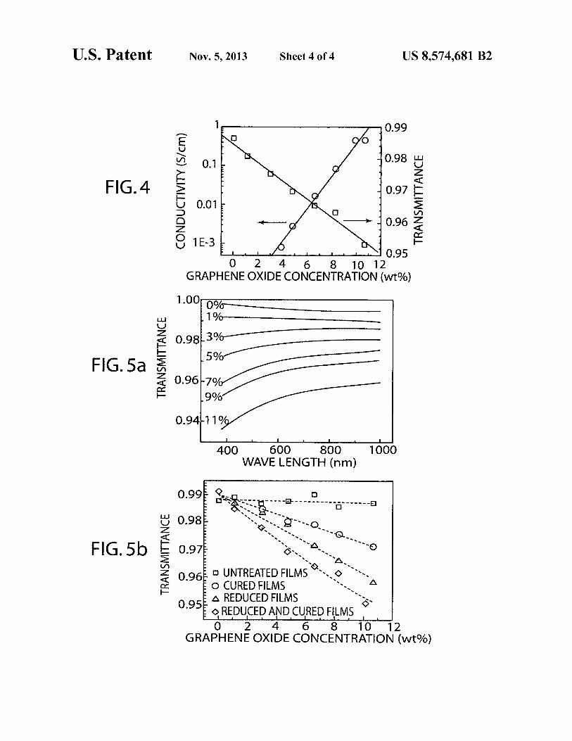
25 FIG. 4 is a plot of bulk electrical conductivity (circles) and light transmittance at 650 mu (squares) of graphene oxide-silica thin films as a function of graphene oxide concentra-tion.
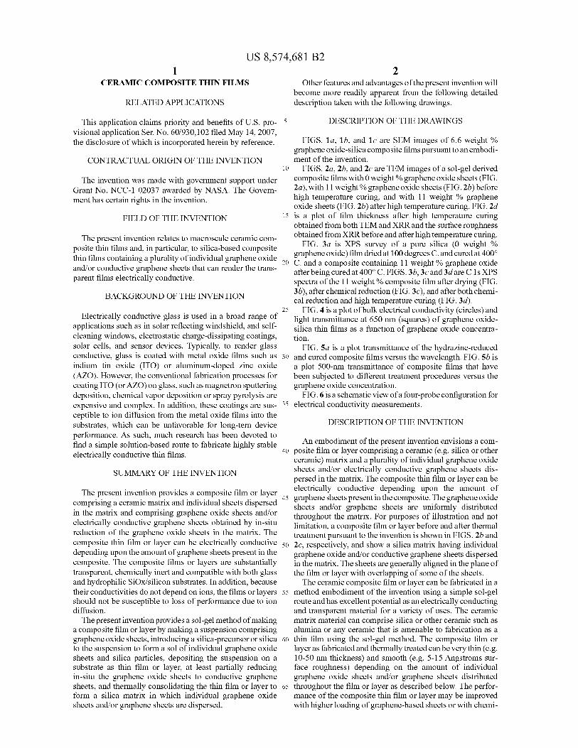
FIG. 5a is a plot transmittance of the hydrazine-reduced 30 and cured composite films versus the wavelength. FIG. 5b is
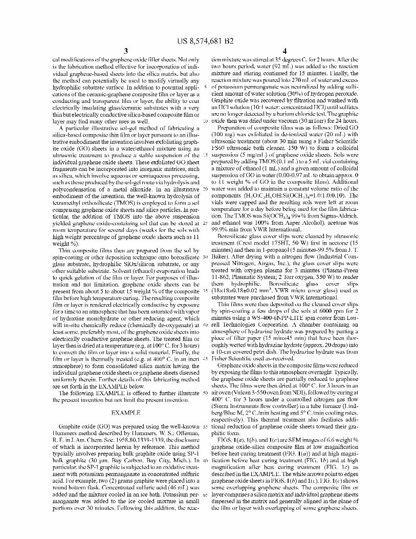
a plot 500-mu transmittance of composite films that have been subjected to different treatment procedures versus the graphene oxide concentration.
FIG. 6 is a schematic view of a four-probe configuration for 35 electrical conductivity measurements.
DESCRIPTION OF THE INVENTION
An embodiment of the present invention envisions a com- 40 posite film or layer comprising a ceramic (e.g. silica or other
ceramic) matrix and a plurality of individual graphene oxide sheets and/or electrically conductive graphene sheets dis-persed in the matrix. The composite thin film or layer can be electrically conductive depending upon the amount of
45 graphene sheets present in the composite. The graphene oxide sheets and/or graphene sheets are uniformly distributed throughout the matrix. For purposes of illustration and not limitation, a composite film or layer before and after thermal treatment pursuant to the invention is shown in FIGS. 2b and
5o 2c, respectively, and show a silica matrix having individual graphene oxide and/or conductive graphene sheets dispersed in the matrix. The sheets are generally aligned in the plane of the film or layer with overlapping of some of the sheets.
The ceramic composite film or layer can be fabricated in a 55 method embodiment of the invention using a simple sol-gel
route and has excellent potential as an electrically conducting and transparent material for a variety of uses. The ceramic matrix material can comprise silica or other ceramic such as alumina or any ceramic that is amenable to fabrication as a
60 thin film using the sol-gel method. The composite film or layer as fabricated and thermally treated can be very thin (e.g. 10-50 nm thickness) and smooth (e.g. 5-15 Angstroms sur-face roughness) depending on the amount of individual graphene oxide sheets and/or graphene sheets distributed
65 throughout the film or layer as described below. The perfor-mance of the composite thin film or layer may be improved with higher loading of graphene-based sheets or with chemi-
US 8,574,681 B2 3
4 cal modifications of the graphene oxide filler sheets. Not only is the fabrication method effective for incorporation of indi-vidual graphene-based sheets into the silica matrix, but also the method can potentially be used to modify virtually any hydrophilic substrate surface. In addition to potential appli-cations of the ceramic-graphene composite film or layer as a conducting and transparent film or layer, the ability to coat electrically insulating glass/ceramic substrates with a very thin but electrically conductive silica-based composite film or layer may find many other uses as well.
A particular illustrative sol-gel method of fabricating a silica-based composite thin film or layer pursuant to an illus-trative embodiment the invention involves exfoliating graph-ite oxide (GO) sheets in a water/ethanol mixture using an ultrasonic treatment to produce a stable suspension of the individual graphene oxide sheets. These exfoliated GO sheet fragments can be incorporated into inorganic matrices, such as silica, which involve aqueous or semiaqueous processing, such as those produced by the sol-gel route via hydrolysis and polycondensation of a metal alkoxide. In an illustrative embodiment of the invention, the well-known hydrolysis of tetramethyl ortrosilicate (TMOS) is employed to form a sol comprising graphene oxide sheets and silica particles. In par-ticular, the addition of TMOS into the above suspension yielded graphene oxide-containing sol that can be stored at room temperature for several days (weeks for the sols with high weight percentage of graphene oxide sheets such as 11 weight %).
Thin composite films then are prepared from the sol by spin-coating or other deposition technique onto borosilicate glass substrate, hydrophilic SiOx/silicon substrate, or any other suitable substrate. Solvent (ethanol) evaporation leads to quick gelation of the film or layer. For purposes of illus-tration and not limitation, graphene oxide sheets can be present from about 5 to about 15 weight % of the composite film before high temperature curing. The resulting composite film or layer is rendered electrically conductive by exposure for a time to an atmosphere that has been saturated with vapor of hydrazine monohydrate or other reducing agent, which will in-situ chemically reduce (chemically de-oxygenate) at least some, preferably most, of the graphene oxide sheets into electrically conductive graphene sheets. The treated film or layer then is dried at a temperature (e.g. at 100° C. for 3 hours) to convert the film or layer into a solid material. Finally, the film or layer is thermally treated (e.g. at 400° C. in an inert atmosphere) to form consolidated silica matrix having the individual graphene oxide sheets or graphene sheets disersed uniformly therein. Further details of this fabricating method are set forth in the EXAMPLE below.
The following EXAMPLE is offered to further illustrate the present invention but not limit the present invention.
EXAMPLE
Graphite oxide (GO) was prepared using the well-known Hummers method described by Hummers, W. S.; Offeman, R. E. in J. Am. Chem. Soc. 1958,80,1339-1339, the disclosure of which is incorporated herein by reference. This method typcially involves preparing bulk graphite oxide using SP-1 bulk graphite (30 µm, Bay Carbon, Bay City, Mich.). In particular, the SP-1 graphite is subjected to an oxidative treat-ment with potassium permanganate in concentrated sulfuric acid. For example, two (2) grams graphite were placed into a round bottom flask. Concentrated sulfuric acid (46 mL) was added and the mixture cooled in an ice bath. Potassium per-manganate was added to the ice cooled mixture in small portions over 30 minutes. Following this addition, the reac-
tion mixture was stirred at 35 degrees C. for 2 hours. After the two hours period, water (92 mL) was added to the reaction mixture and stirring continued for 15 minutes. Finally, the reaction mixture was poured into 270 mL of water and excess
5 of potassium permanganate was neutralized by adding suffi-cient amount of water solution (30%) of hydrogen peroxide. Graphite oxide was recovered by filtration and washed with an HCl solution (10:1 water: concentrated HCl) until sulfates are no longer detected by a barium chloride test. The graphite
io oxide then was dried under vacuum (30 mTorr) for 24 hours. Preparation of composite films was as follows: Dried GO
(100 mg) was exfoliated in de-ionized water (20 mL) with ultrasonic treatment (about 30 min using a Fisher Scientific FS60 ultrasonic bath cleaner, 150 W) to form a colloidal
15 suspension (5 mg/mL) of graphene oxide sheets. Sols were prepared by adding TMOS (0.1 mL) to a 5 mL vial containing a mixture of ethanol (1 mL) and a given amount of colloidal suspension of GO in water (0.00-0.97 mL to obtain approx. 0 to 11 weight % of GO in the composite films). Additional
20 water was added to maintain a constant volume ratio of the components (H20:C2H50H:Si(OCH3)4 1.0:1.0:0.10). The vials were capped and the resulting sols were left at room temperature for a day before being used for the film fabrica-tion. The TMOS was Si(OCH 3)4 99+% from Sigma-Aldrich,
25 and ethanol was 100% from Aaper Alcohol), acetone was 99.9% min from VWR International.
Borosilicate glass cover slips were cleaned by ultrasonic treatment (Crest model 175HT, 50 W) first in acetone (15 minutes) and then in 1-propanol (5 minutes-99.5% from J. T.
3o Baker). After drying with a nitrogen flow (Industrial Com-pressed Nitrogen, Airgas, Inc.), the glass cover slips were treated with oxygen plasma for 3 minutes (Plasma-Preen 11-862, Plasmatic System; 2 Torr oxygen, 350 W) to render them hydrophilic. Borosilicate glass cover slips
35 (18x18x0.18±0.02 mm', VWR micro cover glass) used as substrates were purchased from VWR International.
Thin films were then deposited on the cleaned cover slips by spin-coating a few drops of the sols at 6000 rpm for 2 minutes using a WS-400-6NPP-LITE spin coater from Lau-
4o rell Technologies Corporation. A chamber containing an atmosphere of hydrazine hydrate was prepared by putting a piece of filter paper (15 minx45 min) that have been thor-oughly wetted with hydrazine hydrate (approx. 20 drops) into a 10-cm covered petri dish. The hydrazine hydrate was from
45 Fisher Scientific used as-received. Graphene oxide sheets in the composite films were reduced
by exposing the films to this atmosphere overnight. Typically, the graphene oxide sheets are partially reduced to graphene sheets. The films were then dried at 100° C. for 3 hours in an
5o air oven (Vulcan 3-550 oven from NDI), followed by curing at 400° C. for 3 hours under a controlled nitrogen gas flow (Sierra Instruments flow controller) in a tube furnace (Lind-berg/Blue M, 2° C./min heating and 5° C./min cooling rates, respectively). This thermal treatment also faciliates addi-
55 tional reduction of graphene oxide sheets toward their gra-phitic form.
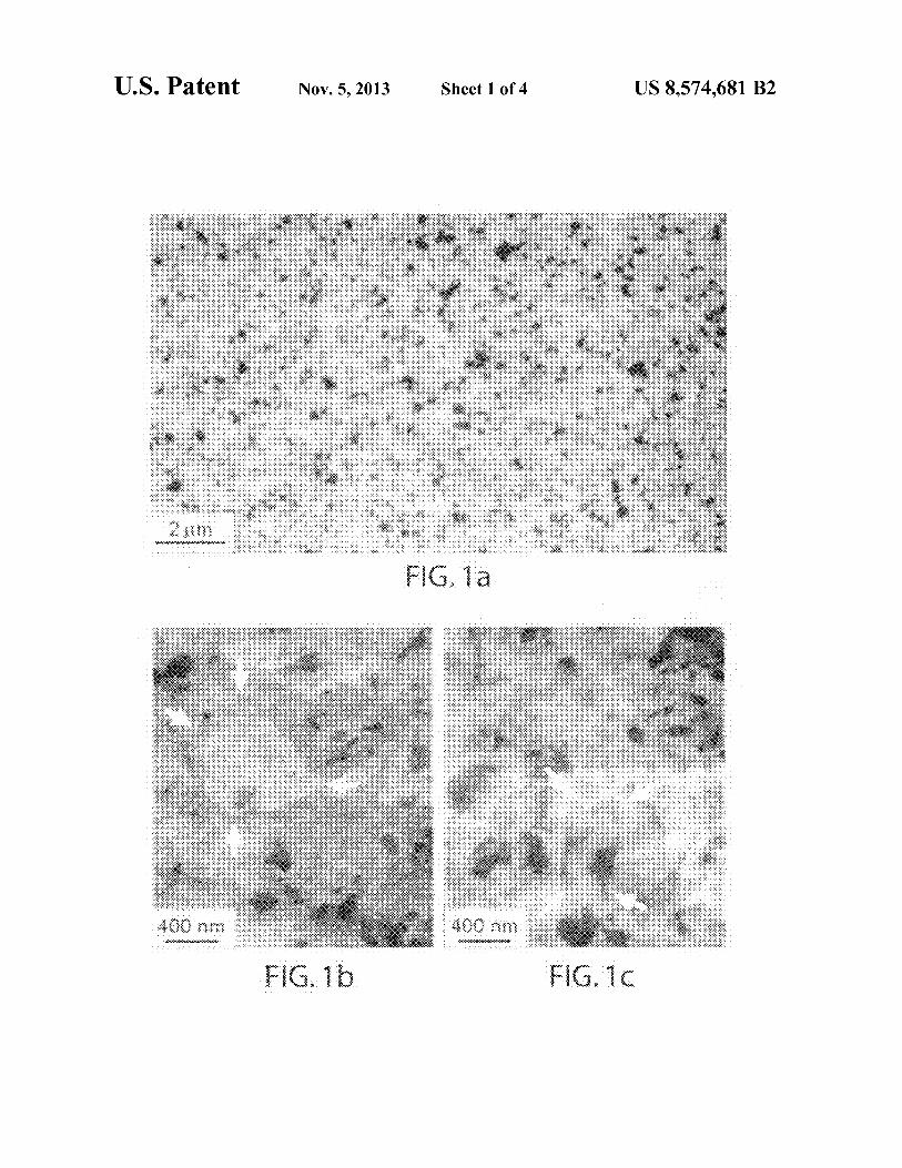
FIGS. 1(a), 1(b), and 1(c) are SEM images of 6.6 weight % graphene oxide-silica composite film at low magnification before heat curing treatment (FIG. 1(a)) and at high magni-
60 fication before heat curing treatment (FIG. lb) and at high magnification after heat curing treatment (FIG. lc) as described in the EXAMPLE. The white arrows point to edges graphene oxide sheets in FIGS. 1(b) and 1(c). FIG. 1(c) shows some overlapping graphene sheets. The composite film or
65 layer comprises a silica matrix and individual graphene sheets dispersed in the matrix and generally aligned in the plane of the film or layer with overlapping of some graphene sheets.
US 8,574,681 B2 5
6
The SEM (scanning electron micrograph) images were that is greater than 100 mm 2 in size), the XRR measurements
acquired on two field emission SEM: using a Nova NanoSEM
are more representative of the average thickness, as the X-ray
600 (FEI Co.) and LEO 1525 (Carl Zeiss SMT AG). The spot size is approx. 1 x20 mm2 .
accelerating voltage was varied between 1-10 keV incident
The average surface roughness of the films was quantified beam energy, depending on the imaging mode and sample 5 by both AFM in contact mode (approx. 10x10 µm 2 area) and properties. XRR (approx. 1 x20 mm2 area). The average surface rough-
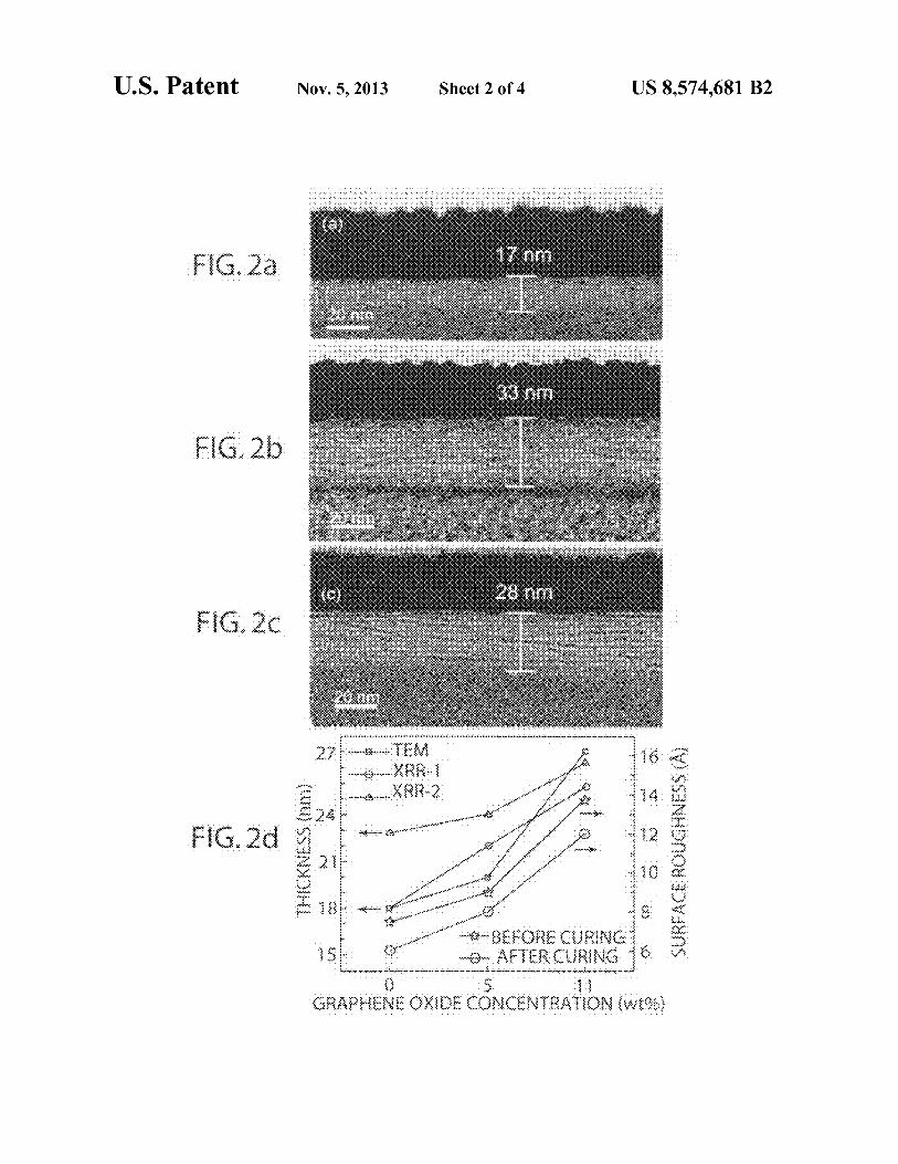
FIGS. 2(a), 2(b), and 2(c) are TEM images of the cross ness of the films increases with increasing concentration of
section of the sol-gel derived composite films with (a) 0
graphene oxide sheets but decreases after curing. For
weight % graphene oxide sheets, (b) 11 wt % of graphene example, from XRR measurement, the sample with a nominal oxide sheets before the high temperature curing and (c) 11 io concentration of 11 wt % graphene oxide sheets had an aver-
weight % of graphene oxide sheets after the high temperature age surface roughness of approx. 14 A before and approx. 12
curing. In these figures, the layers shown are, from the bottom A after curing, while for the 5 wt % sample the values were
of each figure, the glass substrate, composite film, Pt layer, approx. 9 A and approx. 8 A, respectively (FIG. 2d). The
and a carbon layer. FIG. 2(d) illustrates plots of the film surface roughness values given from AFM measurements are thickness of the same samples after high temperature curing 15 similar. The films are thus relatively smooth and geometri-
obtained from both TEM (transmission electron microscopy)
cally uniform over both local regions (AFM) and the entire
and XRR (X-ray reflectivity) and the surface roughness substrate (XRR). XRR data also indicate that the films are
obtained from XRR before and after high temperature curing. reasonably porous (estimated to be from 20-40% less dense
The TEM images were acquired on an JEOL 2100F instru- than the borosilicate glass substrate, depending on humidity ment (JEOL Ltd., Japan) from samples prepared and also cut 20 level) and this density does not change before and after high
as needed by a SEIKO SMI-3050E focused ion beam (FIB)
temperature curing. The density of these composite films
instrument (Seiko Instruments, Japan). To protect the com- remains the same (within the limits of measurement uncer-
posite films, Pt was first deposited onto their surfaces by tainties) over the range of graphene oxide sheet concentra-
sputter coating followed by deposition of a carbon layer by tions employed (1-11 weight %). The AFM analysis involved FIB decomposition of anthracene. The XRR studies were 25 acquiring AFM images taken on an AutoProbe CP/MT scan-
performed at Beam line X23B of the National Synchrotron ning probe microscope (MultiTask; Veeco Instruments).
Light Source (Brookhaven, N.Y.) using a Huber four-circle
Imaging was performed in contact mode using a V-shaped
diffractometer in the specular reflection mode (i.e., incident
`Microlever' probe A (Park Scientific Instruments, Wood-
angle B was equal to the exit angle). The experiments were
bury, N.Y., boron-doped Si tip with spring constant k--0.6 performed at room temperature with 10.0-keV X-rays 3o N/m with frequency f=78.6 kHz and nominal tip radius r=10
(X-1.24 A), and the beam size of 0.4 mm vertically and 1.0
mu). The images were collected under ambient conditions at
mm horizontally. The samples were kept under helium during
23° C. and 50% relative humidity with a scanning rate of 1 Hz.
the measurements to reduce the background scattering from
The topology of the films with 3 weight % GO sheets before
ambient gas and radiation damage. The off-specular back- and after high temperature curing did not show the presence ground was measured and subtracted from the specular 35 of the graphene-based sheets on the surface.
counts. XRR measurements were also carried out using a
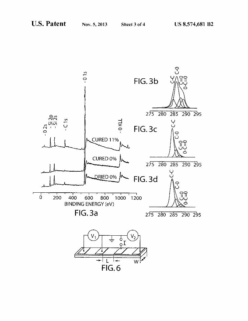
The chemical composition of both the matrix and the GO
Rigaku (The Woodlands, Tex.) ATX-G X-ray diffractometer sheets was monitored by X-ray photoelectron spectroscopy (Cu-Karadiation, 7 =1.544 A). (XPS) during each of the preparation steps. The high tem-
A scanning electron microscopy (SEM) image of a com- perature curing step results in a significant decrease in the posite film containing 6.6 wt % of graphene oxide sheets after 40 carbon content as seen in the survey XPS spectra of the dried
high temperature curing (FIG. la) indicates a homogeneous and cured pure silica film of FIG. 3(a), indicating essentially
morphology with a random distribution of dissimilar black
complete hydrolysis of TMOS. The cured film with 11 weight
and white domains representing tiles of partially overlaping
% graphene oxide sheets exhibited a significantly higher car-
graphene oxide sheets. FIGS. 1(b) and 1(c) contrast high
bon signal compared to that observed for the graphene oxide- magnification SEM images of this same film before and after 45 free film, indicating the presence of the graphene-based filler
high temperature curing. In both images, slightly crumpled
sheets, FIG. 3(a). Specifically, the C is XPS spectrum of the
sheets overlapping each other can be readily observed, indi- composite film with 11 wt % graphene oxidebefore reduction
cating a primarily in-plane orientation. Indeed, such planar and high temperature curing (FIG. 3b) is quite similar to that
distribution of the sheets throughout the film thickness is also of graphite oxide itself. This region can be de-convoluted into evident in the transmission electron microscopy (TEM) 50 four components corresponding to carbon atoms in different
images of the cross sections of the composite film with 11 wt oxygen-containing functional groups: (a) the non-oxygen-
% of graphene oxide sheets both before (FIG. 2b) and after ated C at 284.8 eV, (b) the carbon in C Oat 286.2 eV, (c) the
curing (FIG. 2c). The lack of such features in the graphene carbonyl carbon (C O, 287.9 eV), and (d) the carboxylate
oxide-free silica film (FIG. 2a) suggests that they originate carbon (0—C-0, 289.0 eV). The C is XPS spectra of the from the embedded sheets. 55 hydrazine-treated film shows the presence of the same func-
The thickness of the composite films was determined by tionalities (see FIGS. 3b and 3c) but with much smaller con-
both TEM and X-ray reflectivity (XRR) measurements to be tribution of the oxygenated carbons (27.6% vs. 81.8%), indi-
approx. 20-30 nm thickness, FIG. 2(a)-FIG. 2(c). The varia- cating that de-oxygenation has occurred. In addition, a small
tion in film thickness determined by XRR fitting for different amount of incorporated nitrogen may be present as a conse- samples ranged from ±2 A to ±5 A. Under the conditions 6o quence of exposure to hydrazine.
described in the EXAMPLE, the thickness of the films
The highest levels of DC electrical conductivity were mea-
increased slightly with increasing graphene oxide concentra- sured in the composite films that were both chemically
tion (FIG. 2d). The thickness of the films decreased after the reduced and thermally cured, with the magnitude of electrical
high temperature curing step, indicating densification and
conductivity increasing with the loading of the graphene consolidation of the matrix. While the film thickness obtained 65 oxide. The lowest measured conductivity (resistance less than
from TEM observation is confined to the cross section of a
1 GQ for equipment used) could be observed at loadings as
region smaller than 500 nun across (on a composite sample
low as 3.9 wt % of graphene oxide sheets. As a control, pure
US 8,574,681 B2 7
silica films that were exposed to hydrazine and cured showed no conductivity. The conductivity of the composite films changes by almost three orders of magnitude, from (8.0±0.9)x10-4 S/cm to 0.45±0.06 S/cm, as the loading of graphene oxide increases from 3.9 wt % to 11 wt % (FIG. 4). The chemical reduction step appears to be essential for con-verting insulating graphene oxide sheets into conductive graphene-like sheets and inducing electrical conductivity in composite samples; e.g. the composite films that were sub-jected to high temperature curing without chemical reduction were simply non-conductive.
Chemical reduction alone renders the uncured hydrazine-treated composite films sufficiently conductive to be mea-sured with the testing system described below, but only at higher loading levels of the graphene oxide filler ((I. I tO.1)x 10' S/cm at 11 wt % to (7.0±0.7)x10 -5 S/cm at 9.1 wt %). The combination of chemical reduction and high-temperature treatment significantly improved the overall conductivity of the samples. Presumably, the consolidation of the composite film upon high temperature curing increases the density of the graphene-based sheets inside the silica matrix, reducing the average inter-sheet distances (change of film thickness) and resulting in more pathways for electrical conduction.
The electrical conductivity of the composite films was measured under ambient laboratory conditions using a stan-dard four-probe testing system/method. A Keithley 6221 AC/DC current source and two Keithley 6514 electrometers (Keithley Instruments, Cleveland, Ohio) were connected to the sample using the configuration shown in FIG. 6. Four electrode contacts with an inter-electrode spacing of 0.5 mm were formed onto a cut sample by a thermally evaporating an approx. 20-mu-thick layer of gold (using BOC Edwards Auto 306 Evaporation System) onto a 3 to 5-mm-wide sample strip.
By the four-probe method, the intrinsic resistance (R) of the composite films could be expressed as:
R V2 VI
= ,
where V, and Vz are voltages measured across the electrodes shown in FIG. 4a. The surface resistivity (p J is defined as:
p,=R(w/L),
where w and L are the width and length of the sample area between two adjacent electrodes (FIG. 4a). The bulk conduc-tivity (v) can be calculated as follows:
1
Pst
where t is the film thickness. The uncured hydrazine-treated composite films are suffi-
ciently electrically conductive to be measured with this test-ing system but only at higher loading levels of the graphene oxide filler. The bulk conductivity varies from 1.1 x 10 -3 S/cm at 11 wt % to 7.0x 10 -s S/cm at 9.1 wt % graphene oxide sheets as shown in FIG. 4.
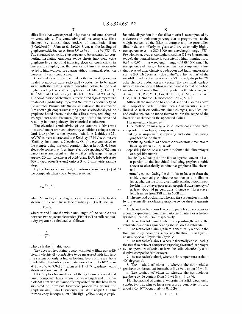
FIG. 5a plots transmittance of the hydrazine-reduced and cured composite films versus the wavelength and FIG. 5b plots 500-nm transmittance of composite films that have been subjected to different treatment procedures versus the graphene oxide sheet concentration. With respect to film transparency, incorporation of the light-yellow opaque graph-
8 ite oxide dispersion into the silica matrix is accompanied by a decrease in their transparency that is proportional to the weight percent of the filler. In comparison, the pure silica films behave similarly to glass and are essentially highly
5 transparent over the 380-1000 mu wavelength range (FIG. 5a). However, even at the highest loading (11 wt % graphene oxide), the transmittance is consistently high, ranging from 0.94 to 0.96 in the wavelength range of 380-1000 mu. The transparency of the graphene oxide-silica composite is fur-
io ther reduced after chemical reduction and high temperature curing (FIG. 5b) primarily due to the "graphenization" of the nanofiller and the transparency at 650 nm only drops by 5% after chemical reduction and curing. The electrical conduc-tivity of the composite films is comparable to that of carbon
15 nanotube-containing thin films reported in the literature; see Xiang, C. S.; Pan, Y. B.; Liu, X. J.; Shi, X. M.; Sun, X. W.; Guo, J. K. J. Nanosci. Nanotechnol. 2006, 6, 1-7.
Although the invention has been described in detail above with respect to certain embodiments, the invention is not
20 limited to such embodiments since changes, modifications and omissions can be made thereot within the scope of the invention as defined in the appended claims.
The invention claimed is: 1. A method of making a solid, electrically conductive
25 composite film or layer, comprising: making a suspension comprising individual insulating
graphene oxide sheets; introducing particles of a ceramic or a ceramic-precursor to
the suspension to form a sol; 30 depositing the sol on a substrate to form a thin film or layer
of a gel-like matrix; chemically reducing the thin film or layer to convert at least
a portion of the individual insulating graphene oxide sheets to electrically conductive graphene-like sheets;
35 and thermally consolidating the thin film or layer to form the
solid, electrically conductive composite thin film or layer, whereinthe solid, electrically conductive compos-ite thin film or layer possesses an optical transparency of
40 at least about 94 percent transmittance within a wave-length range from 380 nm to 1000 mu.
2. The method of claim 1, wherein the suspension is made by ultrasonically exfoliating graphite oxide sheet fragments in water.
45 3. The method of claim 1, wherein particles of a ceramic or a ceramic-precursor comprise particles of silica or a hydro-lyzable silica precursor, respectively.
4. The method of claim 1, wherein depositing the sol on the substrate comprises spin coating the sol on the substrate.
50 5. The method of claim 1, wherein chemically reducing the thin film or layer comprises exposing the thin film or layer to an atmosphere of hydrazine hydrate.
6. The method of claim 1, wherein thermally consolidating the thin film or layer comprises exposing the thin film or layer
55 to a temperature effective to form the solid, electrically con-ductive composite film or layer.
7. The method of claim 6, wherein the temperature is about 400 degrees C.
8. The method of claim 1, wherein the sol includes 60 graphene oxide content from about 3 wt % to about 15 wt %.
9. The method of claim 1, wherein the sol includes graphene oxide content from 3.9 wt % to 11 wt %.
10. The method of claim 9, wherein the solid, electrically conductive thin film or layer possesses a conductivity from
65 about 8.0x10⁻⁴ S/cm to about 0.45 S/cm.