Embed Size (px)
Citation preview
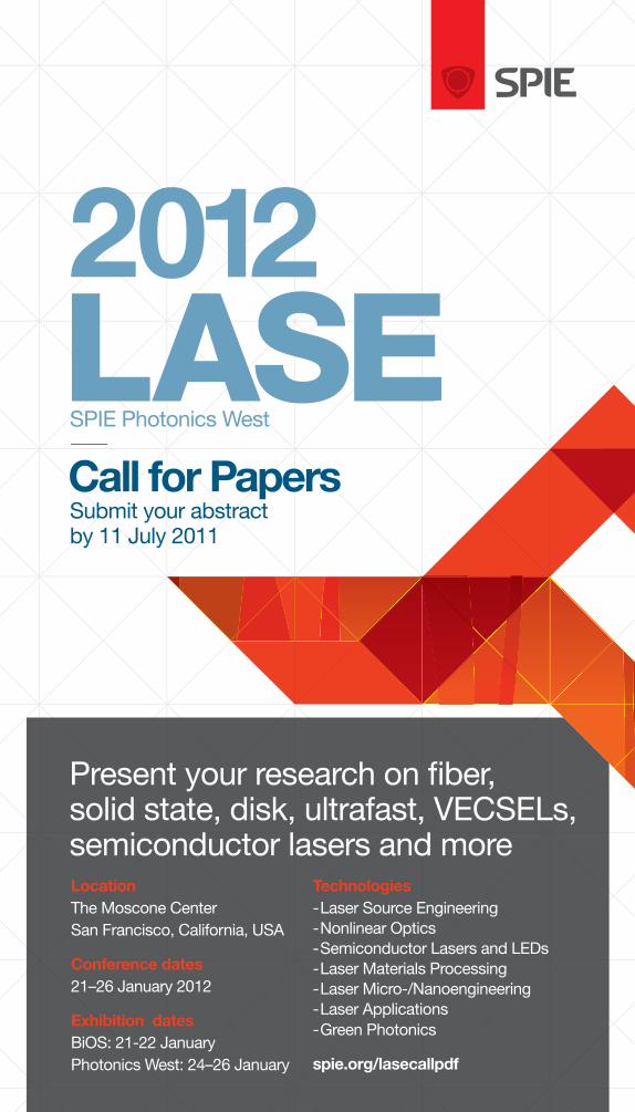
Present your research on fi ber, solid state, disk, ultrafast, VECSELs, semiconductor lasers and more
Technologies- Laser Source Engineering- Nonlinear Optics- Semiconductor Lasers and LEDs- Laser Materials Processing- Laser Micro-/Nanoengineering- Laser Applications- Green Photonics
spie.org/lasecallpdf
LocationThe Moscone CenterSan Francisco, California, USA
Conference dates21–26 January 2012
Exhibition datesBiOS: 21-22 JanuaryPhotonics West: 24–26 January
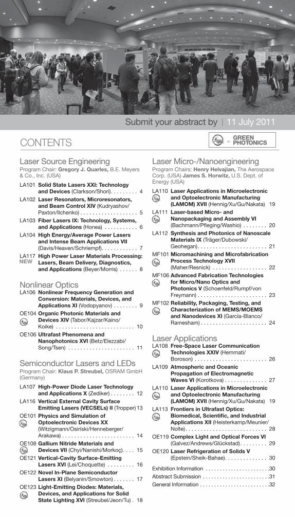
Submit your abstractby 11 July 2011
Call for Papers
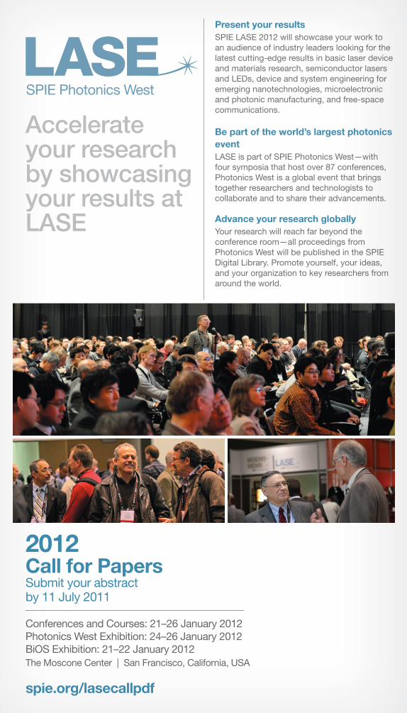
Accelerate your research by showcasing your results at LASE
Present your resultsSPIE LASE 2012 will showcase your work to an audience of industry leaders looking for the latest cutting-edge results in basic laser device and materials research, semiconductor lasers and LEDs, device and system engineering for emerging nanotechnologies, microelectronic and photonic manufacturing, and free-space communications.
Be part of the world’s largest photonics eventLASE is part of SPIE Photonics West—with four symposia that host over 87 conferences, Photonics West is a global event that brings together researchers and technologists to collaborate and to share their advancements.
Advance your research globally Your research will reach far beyond the conference room—all proceedings from Photonics West will be published in the SPIE Digital Library. Promote yourself, your ideas, and your organization to key researchers from around the world.
2012Call for PapersSubmit your abstractby 11 July 2011
spie.org/lasecallpdf
SPIE Photonics West
Conferences and Courses: 21–26 January 2012 Photonics West Exhibition: 24–26 January 2012BiOS Exhibition: 21–22 January 2012The Moscone Center | San Francisco, California, USA
CONTENTS
Laser Micro-/NanoengineeringProgram Chairs: Henry Helvajian, The Aerospace Corp. (USA) James S. Horwitz, U.S. Dept. of Energy (USA)
LA110 Laser Applications in Microelectronic and Optoelectronic Manufacturing (LAMOM) XVII (Hennig/Xu/Gu/Nakata) 19
LA111 Laser-based Micro- and Nanopackaging and Assembly VI (Bachmann/Pfl eging/Washio) . . . . . . . . 20
LA112 Synthesis and Photonics of Nanoscale Materials IX (Träger/Dubowski/Geohegan) . . . . . . . . . . . . . . . . . . . . . . . 21
MF101 Micromachining and Microfabrication Process Technology XVII (Maher/Resnick) . . . . . . . . . . . . . . . . . . 22
MF106 Advanced Fabrication Technologies for Micro/Nano Optics and Photonics V (Schoenfeld/Rumpf/von Freymann) . . . . . . . . . . . . . . . . . . . . . . . 23
MF102 Reliability, Packaging, Testing, and Characterization of MEMS/MOEMS and Nanodevices XI (García-Blanco/Ramesham) . . . . . . . . . . . . . . . . . . . . . . 24
Laser ApplicationsLA108 Free-Space Laser Communication
Technologies XXIV (Hemmati/Boroson) . . . . . . . . . . . . . . . . . . . . . . . . 26
LA109 Atmospheric and Oceanic Propagation of Electromagnetic Waves VI (Korotkova) . . . . . . . . . . . . . . 27
LA110 Laser Applications in Microelectronic and Optoelectronic Manufacturing (LAMOM) XVII (Hennig/Xu/Gu/Nakata) 19
LA113 Frontiers in Ultrafast Optics: Biomedical, Scientifi c, and Industrial Applications XII (Heisterkamp/Meunier/Nolte) . . . . . . . . . . . . . . . . . . . . . . . . . . . 28
OE119 Complex Light and Optical Forces VI (Galvez/Andrews/Glückstad) . . . . . . . . . 29
OE120 Laser Refrigeration of Solids V(Epstein/Sheik-Bahae) . . . . . . . . . . . . . . 30
Exhibition Information . . . . . . . . . . . . . . . . . . . . . . .30Abstract Submission . . . . . . . . . . . . . . . . . . . . . . . .31General Information . . . . . . . . . . . . . . . . . . . . . . . . .32
Laser Source EngineeringProgram Chair: Gregory J. Quarles, B.E. Meyers & Co., Inc. (USA)
LA101 Solid State Lasers XXI: Technology and Devices (Clarkson/Shori) . . . . . . . . . 4
LA102 Laser Resonators, Microresonators, and Beam Control XIV (Kudryashov/Paxton/Ilchenko) . . . . . . . . . . . . . . . . . . . 5
LA103 Fiber Lasers IX: Technology, Systems, and Applications (Honea) . . . . . . . . . . . 6
LA104 High Energy/Average Power Lasers and Intense Beam Applications VII (Davis/Heaven/Schriempf) . . . . . . . . . . . . 7
LA117 High Power Laser Materials Processing: Lasers, Beam Delivery, Diagnostics, and Applications (Beyer/Morris) . . . . . . 8
Nonlinear OpticsLA106 Nonlinear Frequency Generation and
Conversion: Materials, Devices, and Applications XI (Vodopyanov) . . . . . . . . 9
OE104 Organic Photonic Materials andDevices XIV (Tabor/Kajzar/Kaino/Koike) . . . . . . . . . . . . . . . . . . . . . . . . . . 10
OE106 Ultrafast Phenomena and Nanophotonics XVI (Betz/Elezzabi/Song/Tsen) . . . . . . . . . . . . . . . . . . . . . . 11
Semiconductor Lasers and LEDsProgram Chair: Klaus P. Streubel, OSRAM GmbH (Germany)
LA107 High-Power Diode Laser Technology and Applications X (Zediker) . . . . . . . . 12
LA116 Vertical External Cavity Surface Emitting Lasers (VECSELs) II (Tropper) 13
OE101 Physics and Simulation of Optoelectronic Devices XX (Witzigmann/Osinski/Henneberger/Arakawa) . . . . . . . . . . . . . . . . . . . . . . . . 14
OE108 Gallium Nitride Materials and Devices VII (Chyi/Nanishi/Morkoç) . . . . 15
OE121 Vertical-Cavity Surface-Emitting Lasers XVI (Lei/Choquette) . . . . . . . . . 16
OE122 Novel In-Plane Semiconductor Lasers XI (Belyanin/Smowton) . . . . . . . 17
OE123 Light-Emitting Diodes: Materials, Devices, and Applications for Solid State Lighting XVI (Streubel/Jeon/Tu) . 18
Submit your abstract by | 11 July 2011
=
SPIE Photonics West 2012 Call for Papers · spie.org/lasecallpdf2 SPIE Photonics West 2012 Call for Papers · spie.org/lasecallpdf2
Friedrich G. Bachmann, LUMERA LASER GmbH (Germany)
Eckhard Beyer, Fraunhofer-Institut für Werkstoff- und Strahltechnik (Germany)
Don M. Boroson, MIT Lincoln Lab. (USA)
W. Andrew Clarkson, Univ. of Southampton (United Kingdom)
Steven J. Davis, Physical Sciences Inc. (USA)
Jan J. Dubowski, Univ. de Sherbrooke (Canada)
David B. Geohegan, Oak Ridge National Lab. (USA)
Bo Gu, IPG Photonics Corp. (China)
Michael C. Heaven, Emory Univ. (USA)
Alexander Heisterkamp, Laser Zentrum Hannover e.V. (Germany)
Henry Helvajian, The Aerospace Corp. (USA)
Hamid Hemmati, Jet Propulsion Lab. (USA)
Guido Hennig, Daetwyler Graphics AG (Switzerland)
Eric C. Honea, Lockheed Martin Aculight (USA)
James S. Horwitz, U.S. Dept. of Energy (USA)
Executive Organizing Committee
Vladimir S. Ilchenko, OEwaves, Inc. (USA)
Olga Korotkova, Univ. of Miami (USA)
Alexis V. Kudryashov, Moscow State Open Univ. (Russian Federation)
Michel Meunier, Ecole Polytechnique de Montréal (Canada)
Timothy Morris, TRUMPF Inc. (USA)
Yoshiki Nakata, Osaka Univ. (Japan)
Stefan Nolte, Friedrich-Schiller-Univ. Jena (Germany)
Alan H. Paxton, Air Force Research Lab. (USA)
Wilhelm Pfl eging, Karlsruher Institut für Technologie (Germany)
Gregory J. Quarles, B.E. Meyers & Co., Inc. (USA)
J. Thomas Schriempf, Naval Sea Systems Command (USA)
Ramesh K. Shori, Naval Air Warfare Ctr. Weapons Div. (USA)
Klaus P. Streubel, OSRAM GmbH (Germany)
Frank Träger, Univ. Kassel (Germany)
Anne C. Tropper, Univ. of Southampton (United Kingdom)
Konstantin L. Vodopyanov, Stanford Univ. (USA)
Kunihiko Washio, Paradigm Laser Research Ltd. (Japan)
Xianfan Xu, Purdue Univ. (USA)Mark S. Zediker, Foro Energy,
Inc. (USA)
SPIE Photonics West 2012 Call for Papers · spie.org/lasecallpdf2
Symposium ChairStephen J. Eglash Precourt Institute for Energy, Stanford Univ. (USA)
Be part of the solution–present your work in green technologies and be recognized by your peers
keyword in step 4 of the online submission wizard, and upload a 1-2 page summary in step 6. If your paper is selected by Green Photonics selection committee, your work will be eligible to receive additional exposure at Photonics West, including the opportunity to win an SPIE Green Photonics Best Paper Award. Papers are solicited on the following and related topics:
• Solid State Lighting and Displays Effi cient new light sources will provide long-lived
and economical illumination for human activities and information display.
• Laser-assisted Manufacturing and Micro/Nano Fabrication
Optoelectronic sensors and concentrated optical energy sources will enable precision fabrication with low waste.
• Communications The next generation of optical networks will
operate with increased bandwidth and reduced power consumption.
• Renewable Energy Generation: Fusion and Photovoltaics
Small carbon footprint technologies will help meet the world’s increasing demand for energy in a sustainable manner.
The global community recognizes the need for sustainable and renewable energy sources, as well as the need to conserve resources and spur economic growth.
SPIE Green Photonics virtual symposium highlights the latest photonics and optoelectronic tools and materials that will reduce power consumption, enable cleaner manufacturing, and create new energy generation for a broad range of applications.
To be considered for inclusion in the SPIE Green Photonics virtual symposium, when submitting your abstract, enter “GREEN PHOTONICS” as your fi rst
Join the conversation—and get the latest news on SPIE Photonics West
spie.org/connect
#SPIEPW
[email protected] · TEL: +1 360 676 3290 · +1 888 504 8171 [email protected] · TEL: +1 360 676 3290 · +1 888 504 8171 3
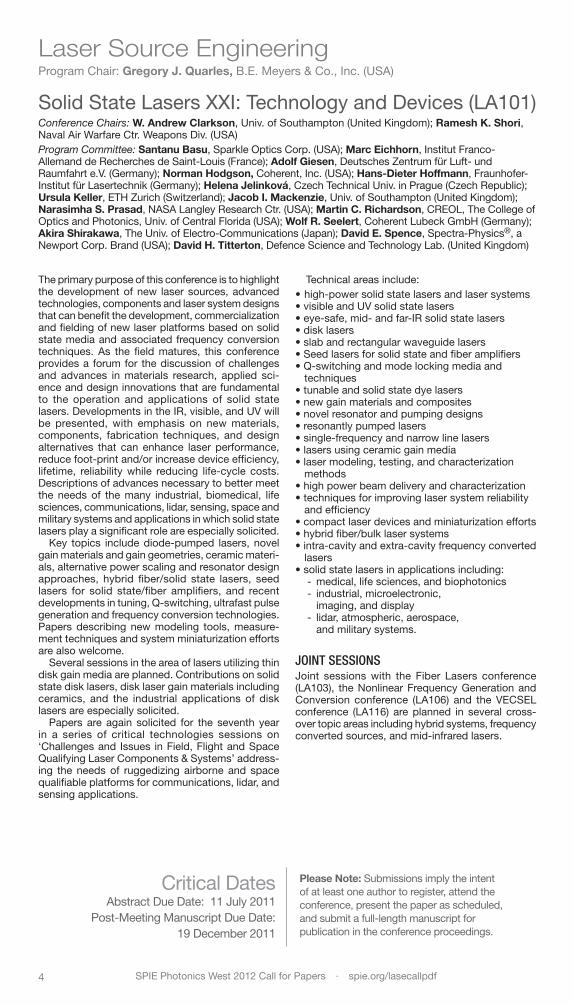
Plan now to participate!SPIE LASE 2012 conferences will address advances in basic laser device research and in laser materials, device and system engineering for various applications ranging from emerging nanotechnologies, microelectronic and photonic manufacturing, and free-space communications, to use on the industrial manufacturing fl oor. In 2012, we have a new conference on High Power Laser Materials Processing: Lasers, Beam Delivery, Diagnostics, and Applications that will address laser manufacturing issues in more detail.
These conferences continue a 22-year tradition of presenting the latest results in Lasers and Applications in Science and Engineering. One of the strengths of this symposium is its ability to bring together people engaged in the full spectrum of laser research and development, from basic research to product manufacturing to system devices and components. Your experience will be enhanced by a plenary session and other networking opportunities, technical courses for professional development, and the co-location with the SPIE Photonics West and BiOS Exhibitions.
We invite all researchers, scientists, engineers, and applications and product developers to join their colleagues and share results related to the conference topics described here.
Present your research at SPIE LASE 2012.
Symposium Chairs Symposium Cochairs
Friedhelm Dorsch, TRUMPF Werkzeugmaschinen GmbH + Co. KG (Germany)
Bo Gu,IPG Photonics Corp. (China)
Andreas Tünnermann,Friedrich-Schiller-Univ. Jena (Germany)
Alberto Piqué, U.S. Naval Research Lab. (USA)
[email protected] · TEL: +1 360 676 3290 · +1 888 504 8171 3
SPIE Photonics West 2012 Call for Papers · spie.org/lasecallpdf4
Laser Source EngineeringProgram Chair: Gregory J. Quarles, B.E. Meyers & Co., Inc. (USA)
Critical DatesAbstract Due Date: 11 July 2011
Post-Meeting Manuscript Due Date: 19 December 2011
Please Note: Submissions imply the intent of at least one author to register, attend the conference, present the paper as scheduled, and submit a full-length manuscript for publication in the conference proceedings.
Solid State Lasers XXI: Technology and Devices (LA101)Conference Chairs: W. Andrew Clarkson, Univ. of Southampton (United Kingdom); Ramesh K. Shori, Naval Air Warfare Ctr. Weapons Div. (USA)Program Committee: Santanu Basu, Sparkle Optics Corp. (USA); Marc Eichhorn, Institut Franco-Allemand de Recherches de Saint-Louis (France); Adolf Giesen, Deutsches Zentrum für Luft- und Raumfahrt e.V. (Germany); Norman Hodgson, Coherent, Inc. (USA); Hans-Dieter Hoffmann, Fraunhofer-Institut für Lasertechnik (Germany); Helena Jelinková, Czech Technical Univ. in Prague (Czech Republic); Ursula Keller, ETH Zurich (Switzerland); Jacob I. Mackenzie, Univ. of Southampton (United Kingdom); Narasimha S. Prasad, NASA Langley Research Ctr. (USA); Martin C. Richardson, CREOL, The College of Optics and Photonics, Univ. of Central Florida (USA); Wolf R. Seelert, Coherent Lubeck GmbH (Germany); Akira Shirakawa, The Univ. of Electro-Communications (Japan); David E. Spence, Spectra-Physics®, a Newport Corp. Brand (USA); David H. Titterton, Defence Science and Technology Lab. (United Kingdom)
The primary purpose of this conference is to highlight the development of new laser sources, advanced technologies, components and laser system designs that can benefi t the development, commercialization and fi elding of new laser platforms based on solid state media and associated frequency conversion techniques. As the fi eld matures, this conference provides a forum for the discussion of challenges and advances in materials research, applied sci-ence and design innovations that are fundamental to the operation and applications of solid state lasers. Developments in the IR, visible, and UV will be presented, with emphasis on new materials, components, fabrication techniques, and design alternatives that can enhance laser performance, reduce foot-print and/or increase device effi ciency, lifetime, reliability while reducing life-cycle costs. Descriptions of advances necessary to better meet the needs of the many industrial, biomedical, life sciences, communications, lidar, sensing, space and military systems and applications in which solid state lasers play a signifi cant role are especially solicited. Key topics include diode-pumped lasers, novel gain materials and gain geometries, ceramic materi-als, alternative power scaling and resonator design approaches, hybrid fi ber/solid state lasers, seed lasers for solid state/fi ber amplifi ers, and recent developments in tuning, Q-switching, ultrafast pulse generation and frequency conversion technologies. Papers describing new modeling tools, measure-ment techniques and system miniaturization efforts are also welcome. Several sessions in the area of lasers utilizing thin disk gain media are planned. Contributions on solid state disk lasers, disk laser gain materials including ceramics, and the industrial applications of disk lasers are especially solicited. Papers are again solicited for the seventh year in a series of critical technologies sessions on ‘Challenges and Issues in Field, Flight and Space Qualifying Laser Components & Systems’ address-ing the needs of ruggedizing airborne and space qualifi able platforms for communications, lidar, and sensing applications.
Technical areas include: • high-power solid state lasers and laser systems • visible and UV solid state lasers • eye-safe, mid- and far-IR solid state lasers • disk lasers • slab and rectangular waveguide lasers • Seed lasers for solid state and fi ber amplifi ers • Q-switching and mode locking media and
techniques • tunable and solid state dye lasers • new gain materials and composites • novel resonator and pumping designs • resonantly pumped lasers • single-frequency and narrow line lasers • lasers using ceramic gain media • laser modeling, testing, and characterization
methods • high power beam delivery and characterization • techniques for improving laser system reliability
and effi ciency • compact laser devices and miniaturization efforts • hybrid fi ber/bulk laser systems • intra-cavity and extra-cavity frequency converted
lasers • solid state lasers in applications including:
- medical, life sciences, and biophotonics - industrial, microelectronic,
imaging, and display - lidar, atmospheric, aerospace,
and military systems.
JOINT SESSIONSJoint sessions with the Fiber Lasers conference (LA103), the Nonlinear Frequency Generation and Conversion conference (LA106) and the VECSEL conference (LA116) are planned in several cross-over topic areas including hybrid systems, frequency converted sources, and mid-infrared lasers.
[email protected] · TEL: +1 360 676 3290 · +1 888 504 8171 5
Cal l fo r Papers
Laser Resonators, Microresonators, and Beam Control XIV (LA102)Conference Chairs: Alexis V. Kudryashov, Moscow State Open Univ. (Russian Federation); Alan H. Paxton, Air Force Research Lab. (USA); Vladimir S. Ilchenko, OEwaves, Inc. (USA)Cochairs: Lutz Aschke, LIMO Lissotschenko Mikrooptik GmbH (Germany); Kunihiko Washio, Paradigm Laser Research Ltd. (Japan)Program Committee: Yanne K. Chembo, FEMTO-ST (France); Jean-Claude M. Diels, The Univ. of New Mexico (USA); Hans Joachim Eichler, Technische Univ. Berlin (Germany); Andrew Forbes, Council for Scientifi c and Industrial Research (South Africa); Pierre Galarneau, INO (Canada); Thomas Graf, Univ. Stuttgart (Germany); Tobias J. Kippenberg, Ecole Polytechnique Fédérale de Lausanne (Switzerland); James R. Leger, Univ. of Minnesota, Twin Cities (USA); Andrey B. Matsko, OEwaves, Inc. (USA); Shayan Mookherjea, Univ. of California, San Diego (USA); Steve A. Pappert, Booz Allen Hamilton Inc. (USA); Andrew W. Poon, Hong Kong Univ. of Science and Technology (Hong Kong, China); Michelle L. Povinelli, The Univ. of Southern California (USA); Michael Scaggs, Neoteric Concepts, LLC (USA); Lan Yang, Washington Univ. in St. Louis (USA)
Laser resonators may be considered to be the heart of any laser system and mainly determine the output beam quality of any type of laser. Therefore resonator design may be the solution of various scientifi c and technological problems. Controlling the shape of laser beams is central to all laser applications and is an enabling factor for the application of lasers in new technologies and applications. This confer-ence will explore new and novel approaches to the beam shaping of laser radiation with low and high power levels and the design of laser resonators with various nonstandard optical elements and systems. Also new criteria for laser beam characterization of lasers and amplifi ers, and beam and pulse formation in lasers will be discussed. Optical microresonators have become a distinct and growing subject of research, development and optical engineering as building blocks in variety of applications ranging from micro-lasers, laser stabilization, through nonlinear- and quantum op-tics devices and experiments, to fi lters, sensors, radio-frequency and terahertz oscillators, lightwave circuits and signal processors. In this conference we intend to explore all areas of optical microresonators fi eld, including latest developments in microcavity optomechanics, resonant optical cooling, optical frequency comb generation, and phonon lasing. Conference papers are solicited on a wide range of topics related to the conference title, including but not limited to the following:
Laser Resonators: • active and adaptive laser resonators • stable and unstable laser resonators for high-
quality laser beams • resonators for gas, solid state, and fi ber lasers • high-stability laser resonators.
Beam Shaping and Beam Control of Specifi c Lasers: • collimation of the output beams of laser diodes • fi ber coupling of diode lasers • lasers with phase conjugation and their
applications • femtosecond lasers: beam and pulse control and
formation • laser beam homogenization • Gauss to top hat conversion • line focus generation • generation of application specifi c intensity
distributions • beam shaping of multi KW lasers • new optical elements and systems for lasers • applications with specifi c laser beam geometries • laser-beam characterization and measurement of
laser-beam parameters
• spatial stabilization of laser beam shapes • beam delivery systems • feedback and control systems for aiming,
frequency stabilization, or energy absorption. • high power and high-brightness beam
delivery optics, including advanced isolators, connectors, beam switches, etc.
• high speed beam steering devices, including KTN scanners, etc.
• advanced beam shapers and spatial light modulators for smart laser processing, etc.
• novel polarization and angular momentum state conversion devices and technologies.
Microresonators, Properties and Applications: • microcavity fundamentals: novel resonator
topologies, morphologies, coupling methods; novel resonator materials, mechanisms of optical losses and quality-factor limitations
• multiresonator structures: resonator chains, 2D and 3D structures
• fabrication technologies and their limitations, device integration, packaging and stability factors
• microcavity-based and microcavity-stabilized lasers: self-injection locked lasers, functionalization and gain media, resonant SRS and resonant SBS with microcavities
• nonlinear optical phenomena with microresonators: optical frequency combs and parametric oscillators with microresonators, microresonator-based plasmonics and polaritonics
• microwave and TeraHertz photonics with microcavities: resonant microwave photonic modulators and receivers, microwave photonic oscillators, microwave photonic fi lters, arbitrary waveform generation
• cavity quantum electrodynamics and quantum optics with microresonators: atom-photon interactions, solid state spectrometry, multiphoton spectroscopy, zero-phonon-line spectroscopy with microcavities; microcavities and quantum dots
• microcavity optomechanics: laser cooling of mesoscopic mechanical degrees of freedoms, stimulated phonon emission, microparticle manipulations and transport
• sensor applications with microresonators: accelerometry, vibrometry, temperature, pressure, biochemical and trace gas sensors, single molecule detection, microresonators in microfl uidics and gyroscopes
• novel and emerging applications of microresonators.
SPIE Photonics West 2012 Call for Papers · spie.org/lasecallpdf6
Laser Source Eng ineer ing
Conference Cosponsors
Fiber Lasers IX: Technology, Systems, and Applications (LA103)Conference Chair: Eric C. Honea, Lockheed Martin Aculight (USA)Cochair: Sami T. Hendow, Multiwave Photonics (USA)Program Committee: John Ballato, Clemson Univ. (USA); Jes Broeng, NKT Photonics A/S (Denmark); Adrian L. G. Carter, Nufern (USA); John R. Clowes, Fianium Ltd. (United Kingdom); Jay W. Dawson, Lawrence Livermore National Lab. (USA); Fabio Di Teodoro, Northrop Grumman Aerospace Systems (USA); Mark Dubinskii, U.S. Army Research Lab. (USA); Jean-Philippe M. Fève, Directed Energy Solutions (USA); Almantas Galvanauskas, Univ. of Michigan (USA); Denis V. Gapontsev, Consultant (Russian Federation); Clifford Headley III, OFS Labs. (USA); Yoonchan Jeong, Seoul National Univ. (Korea, Republic of); Dahv A. Kliner, JDSU (USA); John D. Minelly, Coherent, Inc. (USA); Peter F. Moulton, Q-Peak, Inc. (USA); Siddharth Ramachandran, The Boston Univ. Photonics Ctr. (USA); L. Brandon Shaw, U.S. Naval Research Lab. (USA); Daniel B. Soh, Sandia National Labs., California (USA); James R. Taylor, Imperial College London (United Kingdom); Andreas Tünnermann, Friedrich-Schiller-Univ. Jena (Germany) and Fraunhofer-Institut für Angewandte Optik und Feinmechanik (Germany); Robert G. Waarts, Robert Waarts Consulting (USA); Ji Wang, Corning Incorporated (USA); Frank W. Wise, Cornell Univ. (USA); David E. Zelmon, Air Force Research Lab. (USA); Clint Zeringue, Air Force Research Lab. (USA); Mikhail N. Zervas, Univ. of Southhampton (United Kingdom)
As research, development, and deployment of fi ber lasers continues to expand, the Fiber Lasers Confer-ence at Photonics West has become the preeminent conference in the fi eld. Drawing leading researchers from universities, laboratories, and industry, it pro-vides a comprehensive update in all areas of fi ber lasers and amplifi ers. A list of topics is provided below, and submissions are encouraged in all areas relevant to fi ber laser technology and applications. Submissions must be completed by 11 July 2011. Topics include:
Fiber Lasers and Amplifi ers • novel laser designs • power scaling to high average powers and high
peak powers • Q-switched, mode-locked, and ultrafast fi ber
lasers, including chirped-pulse amplifi ers • Programmable pulse shaping, waveform
generation or wavelength tuning fi ber sources• UV, visible, near-IR, and mid-IR fi ber sources • narrow-linewidth sources • broadband fi ber sources• random or incoherent fi ber lasers• laser diode pump coupling and pumping
methods • frequency conversion • beam combination − coherent, spectral, and
geometric; active and passive • beam guiding and propagation in multimode
fi bers • modeling of waveguides, lasers, and amplifi ers,
including nonlinear processes • modeling of thermal effects in high power fi ber
laser systems and applications • packaging of high power fi ber laser systems • measurement techniques for high-power fi ber
sources • hybrid fi ber/bulk lasers.
Fiber Fabrication and Design: Fiber Optical Components • fabrication processes • characterization techniques • novel fi bers and new dopants • photodarkening and reliability • polarization control • mechanisms of index change • grating fabrication and devices • couplers, switches, modulators, fi lters, and
isolators • fi ber processing, components, and delivery
optics for high-power applications.
Applications • sensing • materials processing • microfabrication • frequency metrology • biomedical sciences • defense • novel devices for communications • commercial aspects of fi ber lasers.
JOINT SESSIONS Joint sessions with the Solid State Lasers confer-ence (LA101) and Nonlinear Frequency Generation and Conversion conference (LA106) are possible in several cross-over topic areas, including hybrid fi ber-bulk systems, frequency converted sources, and high-power beam delivery and characterization.
Extended Abstracts Encouraged Contributions are accepted based on a peer reviewing process, and contributors are encouraged to submit up to two pages of additional information (including fi gures) for use in the review (in addition to the 100- and 250-word abstracts submitted that are suitable for publication). In order to be accepted for an oral talk, it is important that the additional information clearly distinguish the work to be presented from prior work.
[email protected] · TEL: +1 360 676 3290 · +1 888 504 8171 7
Cal l fo r Papers
Submit your abstract today!
spie.org/lasecallpdf
High Energy/Average Power Lasers and Intense Beam Applications VII (LA104)Conference Chairs: Steven J. Davis, Physical Sciences Inc. (USA); Michael C. Heaven, Emory Univ. (USA); J. Thomas Schriempf, Naval Sea Systems Command (USA)Program Committee: David L. Carroll, CU Aerospace LLC (USA); Jarmila Kodymová, Institute of Physics of the ASCR, v.v.i. (Czech Republic); Timothy J. Madden, Air Force Research Lab. (USA); William E. McDermott, Univ. of Denver (USA); Wilson T. Rawlins, Physical Sciences Inc. (USA)
Gas and chemical lasers remain the laser systems most easily scalable to very high-energies and average-powers including megawatt class lasers for military applications and tens of kilowatt class lasers for industrial applications. This conference solicits papers in all areas of gas and chemical lasers including: HF/DF, CO, CO2, and COIL and their applications. New hybrid lasers such as the electrical oxygen iodine laser (EOIL) and optically pumped gas phase lasers including the diode laser pumped alkali lasers (DPAL) will be included. This conference is envisioned to provide a good cross-section of different aspects of laser development and applications. • Papers on basic kinetics, thermodynamics, spectroscopy,
modeling, and new designs are solicited. • Scaling of lasers for high-peak powers, high-average powers
and special pulse formatting for specifi c applications are of interest.
• Applications including lidar, materials cutting, surface treatment and surface modifi cations and other intense beam applications are especially solicited.
• With the rapid progress in high-power fi ber lasers and diode-pumped solid state lasers, we also encourage contributions that discuss recent results in these devices, especially in the area of high-power applications.
• Papers on current progress of existing systems will be integrated into the conference to show the applications of knowledge generated by break-through technological developments.
JOINT SESSION WITH LA109 (Atmospheric and Oceanic Propagation of Electromagnetic Waves VI)Atmospheric propagation of high power laser beams to include aerosol effects, thermal blooming, and turbulence, particularly at those wavelengths relevant to chemical and hybrid lasers.
Post Deadline Session There will be a post deadline session held to report on late breaking work with signifi cant impact. Submissions to this session will be through the SPIE web site beginning October 2011 and may be submitted as late as 10 January 2012. A limited number of high quality papers will be accepted to the post-deadline session regard-less of the number of submissions. Two-page submissions are required. Accepted papers will be printed as submitted without further revision in the front matter of the proceedings (the front matter is not citable like manuscripts are). Papers are selected and announced the week prior to the conference, so you must be prepared to attend and present before you even know if your paper will be accepted.
Best Student Presentation AwardsA cash prize donated by our cospon-sors will be awarded to the best and runner-up student presentations. To be considered, nominate yourself during STEP 4 of the abstract sub-mission wizard (under Topic Area, select “Consider for Best Student Presentation” as your First Choice). Presentations will be judged based on scientifi c merit, impact, and clar-ity. While the award is not judged by the manuscript, a manuscript must be submitted to the conference Proceedings.
SPIE Photonics West 2012 Call for Papers · spie.org/lasecallpdf8
Laser Source Eng ineer ing
NEWHigh Power Laser Materials Processing: Lasers, Beam Delivery, Diagnostics, and Applications (LA117)Conference Chairs: Eckhard Beyer, Fraunhofer-Institut für Werkstoff- und Strahltechnik (Germany); Timothy Morris, TRUMPF Inc. (USA)Program Committee: Milan Brandt, RMIT Univ. (Australia); Craig Bratt, Fraunhofer USA, Inc. (USA); Edward Chlebus, Wroclaw Univ. of Technology (Poland); Ingomar Kelbassa, RWTH Aachen (Germany); Wolfgang Knapp, Cooperation Laser Franco-Allemande (France); Isamu Miyamoto, Osaka Univ. (Japan); Thomas P. Pearsall, European Photonics Industry Consortium (France); Silke Pfl ueger, Laserline Inc. (USA); Michael Schmidt, Friedrich-Alexander-Univ. Erlangen-Nürnberg (Germany); Anja Techel, Fraunhofer-Institut für Werkstoff- und Strahltechnik (Germany); Luigi Tricarico, Politecnico di Bari (Italy); Kunihiko Washio, Paradigm Laser Research Ltd. (Japan); Minlin Zhong, Tsinghua Univ. (China)
High power lasers are utilized in a myriad of industrial settings. There are several key laser technologies employed for materials processing and each laser type, wavelength and architecture has its advantages and key applications where it excels. The laser, however, is only part of the story. Delivering the beam to the work piece, and monitoring both the beam characteristics, as well as the process, are important enablers for any given application. This conference will explore high power lasers, how they are delivered to the work piece, how they and the process are monitored, and their uses in the world of industrial materials processing. Pa-pers are solicited on a wide range of topics related to the conference title, including but not limited to the following:
Lasers and Laser Systems for Materials Processing: • disk• fi ber• direct diode• CO2.
Beam Delivery: • welding heads and accessories• scanning heads• cutting heads and accessories• LMD heads and accessories• Beam shaping methods• thermal lensing and optics design approaches• new optical elements and systems for lasers • applications with specifi c laser beam
geometries.
Diagnostics: • laser-beam characterization and measurement of
laser-beam parameters • laser material interaction• process monitoring• vision systems and tracking• destructive and non-destructive quality testing
methods• surface diagnostics• coupling experiments and simulations• high speed imaging• particulate diagnostics• systems considerations.
Applications: • welding• remote welding• brazing / soldering• hybrid welding• laser metal deposition• hardening• cutting• remote cutting• drilling• cleaning and structuring• rapid prototyping and manufacturing.
[email protected] · TEL: +1 360 676 3290 · +1 888 504 8171 9
Nonlinear Optics
Nonlinear Frequency Generation and Conversion: Materials, Devices, and Applications XI (LA106)Conference Chair: Konstantin L. Vodopyanov, Stanford Univ. (USA)Cochair: Yehoshua Y. Kalisky, Nuclear Research Ctr. Negev (Israel)Program Committee: Darrell J. Armstrong, Sandia National Labs. (USA); Pinhas Blau, Soreq Nuclear Research Ctr. (Israel); Majid Ebrahim-Zadeh, ICFO - Instituto de Ciencias Fotónicas (Spain); Peter P. Günter, ETH Zurich (Switzerland); Angus J. Henderson, Lockheed Martin Aculight (USA); Baldemar Ibarra-Escamilla, Instituto Nacional de Astrofísica, Óptica y Electrónica (Mexico); Yun-Shik Lee, Oregon State Univ. (USA); Rita D. Peterson, Air Force Research Lab. (USA); Peter E. Powers, Univ. of Dayton (USA); Kenneth L. Schepler, Air Force Research Lab. (USA); Peter G. Schunemann, BAE Systems (USA); Andrei V. Shchegrov, Andrei Shchegrov Consulting (USA); Wei Shi, NP Photonics, Inc. (USA); Ramesh K. Shori, Naval Air Warfare Ctr. Weapons Div. (USA)
The purpose of this conference is to provide a forum for discussing advances in nonlinear optics. Areas of emphasis include novel nonlinear materials (particularly engineered and waveguide structures), new devices and techniques for improved nonlinear frequency conversion, and application demonstra-tions based upon nonlinear devices. Topics include:
Nonlinear Materials• bulk inorganic and organic nonlinear materials• engineered nonlinear materials for quasi-phase
matching• semiconductors and quantum-well structures for
nonlinear conversion• nanostructures• photonic bandgap enhanced interactions• nonlinear fi bers, waveguides and thin fi lms• novel nonlinear materials• crystal growth• measurements and measurement techniques of
nonlinear optical properties.
Devices and Techniques• nonlinear processes in bulk crystals, fi bers,
waveguides and thin fi lms• parametric frequency conversion• quasi-phase matching• frequency-agile tuning• stimulated Raman and Brillouin scattering• multi-photon absorption• optical solitons• optical pulse compression• self-organized fi ber gratings• four-wave mixing• modeling.
Applications• chemical and biological sensing, remote sensing• materials processing• optical storage• optical communications• optical switching• frequency combs and optical clocks• THz generation, spectroscopy and imaging• frequency combs generation.
JOINT SESSIONSJoint sessions with the Fiber Lasers conference (LA103) and the Solid State Lasers conference (LA101) are planned in cross-over topic areas.
Published by SPIE
Get the Latest Research
SPIEDigitalLibrary.org
SPIE Photonics West 2012 Call for Papers · spie.org/lasecallpdf10
Nonl inear Opt ics
This conference of related interest is part of OPTO 2012 co-located at Photonics West, spie.org/optocall.
Organic Photonic Materials and Devices XIV (OE104)Conference Chairs: Christopher Tabor, Air Force Research Lab. (USA); François Kajzar, Polytechnical Univ. of Bucharest (Romania); Toshikuni Kaino, Tohoku Univ. (Japan); Yasuhiro Koike, Keio Univ. (Japan)Program Committee: Chantal Andraud, Ecole Normale Supérieure de Lyon (France); Werner J. Blau, Trinity College Dublin (Ireland); Christoph Bubeck, Max-Planck-Institut für Polymerforschung (Germany); Fabrice Charra, Commissariat à l’Énergie Atomique (France); Darnell E. Diggs, Air Force Research Lab. (USA); Raluca Dinu, GigOptix, Inc. (USA); Alain F. Fort, Institut de Physique et Chimie des Matériaux de Strasbourg (France); James G. Grote, Air Force Research Lab. (USA); Frank K. Hopkins, Air Force Research Lab. (USA); Alex K. Jen, Univ. of Washington (USA); Michael H. C. Jin, The Univ. of Texas at Arlington (USA); Eunkyoung Kim, Yonsei Univ. (Korea, Republic of); Jang-Joo Kim, Seoul National Univ. (Korea, Republic of); Nakjoong Kim, Hanyang Univ. (Korea, Republic of); Junya Kobayashi, NTT Photonics Labs. (Japan); Isabelle N. Ledoux-Rak, École Normale Supérieure de Cachan (France); Charles Y. C. Lee, Air Force Offi ce of Scientifi c Research (USA); Kwang-Sup Lee, Hannam Univ. (Korea, Republic of); Emisoon Mah, Air Force Research Lab. (USA); Seth R. Marder, Georgia Institute of Technology (USA); Antoni C. Mitus, Wroclaw Univ. of Technology (Poland); Robert L. Nelson, Air Force Research Lab. (USA); Robert A. Norwood, College of Optical Sciences, The Univ. of Arizona (USA); Jean-Michel Nunzi, Queen’s Univ. (Canada); Susanna Orlic, Technische Univ. Berlin (Germany); Ileana Rau, Polytechnical Univ. of Bucharest (Romania); Niyazi Serdar Sariciftci, Johannes Kepler Univ. Linz (Austria); Devanand K. Shenoy, Defense Advanced Research Projects Agency (USA); Kenneth D. Singer, Case Western Reserve Univ. (USA); Don J. Smith, U.S. Air Force (United Kingdom); Attila A. Szep, Air Force Research Lab. (USA); Rebecca E. Taylor, Lockheed Martin Space Systems Co. (USA); Toshiyuki Watanabe, Tokyo Univ. of Agriculture and Technology (Japan); Shiyoshi Yokoyama, Kyushu Univ. (Japan); Roberto Zamboni, Consiglio Nazionale delle Ricerche (Italy)
There is a growing interest and a revolution in or-ganic/polymeric photonic and electronic materials and devices for telecommunication, data commu-nication, storage, display and other applications. Recent advances in the development of electro-luminescent and electro-optic devices as well as planar lightwave circuits suggest that organic and polymeric materials will play a signifi cant role in this area. Organic-inorganic hybrid materials are also of special concern for novel photonic device develop-ment. Organic Photonic Materials and Devices XII will serve as a forum for the dissemination and discus-sion of state-of-the-art results pertaining to organic opto-electronic, nano-photonic and biophotonic materials and devices as well as their applications. The objective of this conference is to bring to-gether researchers and engineers from academia, industry, and government laboratories who share a common interest in organic photonic materials and devices. Emphasis will be placed on organic materials and devices, with additional sessions on applications. This conference will provide a forum for an update on progress in the highly connected and multidisci-plinary subject of photonic technologies based on organic materials.
Papers are solicited in the following areas:
• nonlinear optical polymer materials and devices • organic electroluminescent materials and
devices • photorefractive materials and processes • photochromic materials • polymer optical waveguides and fi bers • multiphoton processes • charge transport in organic materials • single molecule spectroscopy • organic fi eld effect transistors • polymer lasers and amplifi ers • optical limiting materials • polymer solar cells and photodetectors • nano-photonics and organic metamaterials • biophotonics • biopolymers • organic-inorganic hybrid materials and devices • fl exible semiconductors • plasmonic NLO effects • polymeric photonic crystals • hybrid organic-inorganic materials • multiphoton processes • theoretical description of NLO processes • Rf organic materials properties.
Green Photonics Virtual SymposiumPresent your technology solution for:
• Energy conservation
• Renewable energy generation
• Effi cient light sourcesSee page 2 for details.
[email protected] · TEL: +1 360 676 3290 · +1 888 504 8171 11
Cal l fo r Papers
This conference of related interest is part of OPTO 2012 co-located at Photonics West, spie.org/optocall.
Ultrafast Phenomena and Nanophotonics XVI (OE106)Conference Chairs: Markus Betz, Technische Univ. Dortmund (Germany); Abdulhakem Y. Elezzabi, Univ. of Alberta (Canada); Jin-Joo Song, Univ. of California, San Diego (USA); Kong-Thon Tsen, Arizona State Univ. (USA)Program Committee: Mischa Bonn, FOM Institute for Atomic and Molecular Physics (Netherlands); Yujie J. Ding, Lehigh Univ. (USA); Jan A. Gaj, Univ. of Warsaw (Poland); Kazuhiko Hirakawa, The Univ. of Tokyo (Japan); Rupert Huber, Univ. Regensburg (Germany); Robert A. Kaindl, Lawrence Berkeley National Lab. (USA); Dai-Sik Kim, Seoul National Univ. (Korea, Republic of); Torsten Meier, Univ. Paderborn (Germany); Walter Pfeiffer, Univ. Bielefeld (Germany); Mark I. Stockman, Georgia State Univ. (USA); Chi-Kuang Sun, National Taiwan Univ. (Taiwan); Fabrice Vallee, Univ. Claude Bernard Lyon 1 (France); Klaas Wynne, Univ. of Strathclyde (United Kingdom); Chih-Chung Yang, National Taiwan Univ. (Taiwan)
This conference covers ultrafast phenomena in bulk semiconductors, semiconducting and metallic nano-structures, devices, and lasers with emphasis on ultrafast optical, coherent and transport phenomena. Manuscripts are solicited in the following topics but not restricted to:
Ultrafast carrier and exciton dynamics • carrier-carrier, carrier-phonon interactions • formation, recombination dynamics of excitons • non-equilibrium phonon effects • polariton dynamics in microcavities.
Coherent dynamics of optical excitations • excitonic coherence and phase breaking • quantum interference effects • four-wave mixing, two-dimensional
spectroscopy • coherent phonons.
Non-linear optical effects • optical frequency conversion • multi-photon processes, high-fi eld physics • high harmonic generation, attosecond physics • ultrafast probing of surfaces and interfaces.
Non-equilibrium carrier transport • ballistic carrier transport, overshoot effects • tunneling phenomena • Bloch oscillations.
Ultrafast phenomena in wide-gap semiconductors • ultrafast carrier transport, relaxation • carrier-phonon, phonon-phonon interactions • hot phonon effects.
Spin dynamics and spin manipulation • ultrafast optical spin manipulation • spin coherence and relaxation • photoinduced magnetization dynamics • spin injection and transport • spin echo techniques.
Ultrafast plasmonics• active plasmonics • THz plasmonics • ultrafast dynamics in metallic nanostructures.
THz spectroscopy• THz wave generation • fi eld-resolved techniques • THz time-domain spectroscopy • applications of THz radiation.
Ultrafast processes in devices and lasers • ultrafast optical switching • gain dynamics in lasers and amplifi ers • propagation and amplifi cation laser pulses.
Ultrafast nano-optics • nanoemitters, nanoantennae • nanolocalization of optical fi elds • coherent control in nanostructures • semiconductor quantum dots and wires • single-photon sources • applications for quantum information
processing.
Ultrafast optical properties of metamaterials• photonic and phononic crystals • metal-semiconductor hybrid structures • negative-index materials • metatronics.
2012 Keynote speaker: Nader Engheta, University of Pennsylvania (USA)
SPIE Photonics West 2012 Call for Papers · spie.org/lasecallpdf12
Semiconductor Lasers and LEDsProgram Chair: Klaus P. Streubel, OSRAM GmbH (Germany)
High-Power Diode Laser Technology and Applications X (LA107)Conference Chair: Mark S. Zediker, Foro Energy, Inc. (USA)Program Committee: Friedrich G. Bachmann, LUMERA LASER GmbH (Germany); Stefan W. Heinemann, Fraunhofer USA, Inc. (USA); Volker K. Krause, Laserline GmbH (Germany); Kurt J. Linden, Spire Corp. (USA); Robert J. Martinsen, nLIGHT Corp. (USA); Erik P. Zucker, JDSU (USA)
The High-Power Diode Laser Technology and Ap-plications conference intends to gather people to discuss the latest developments in high power laser diode technology and how the technology is being used. The conference will include discussions on high power diode laser devices, high power diode laser bars, high power diode laser arrays, coherent beam combining of high power diode laser, spec-tral beam combining of high power diode lasers, frequency stabilization of high power laser diodes, fi ber coupling of high power diode laser arrays, reli-ability of high power diode lasers, high effi ciency, high temperature operation of diode laser arrays, short wavelength high power diode lasers and high power diode lasers for display applications. The focus of this conference is to discuss new develop-ments in the high power diode laser technology and how these new devices are being integrated into applications. Papers are solicited on a wide range of topics related to high-power diode laser technology and applications, including but not limited to: • high-power diode lasers single emitters, mini-
bars and array technology • reliability of high-power diode laser devices and
packages • high-brightness diode laser technology • mounting and cooling of high-power diode laser
bars and arrays • beam formation with high-power diode laser
arrays • beam combining of high-power diode lasers and
arrays • frequency stabilization of high-power laser
diodes and arrays • fi ber coupling of high-power diode lasers and
arrays • operating costs, effi ciency, life considerations • unique applications of new high power, high
brightness laser diode devices• high power visible and mid-IR diode lasers and
applications.
Extended Abstracts Encouraged Contributions are accepted based on a peer review-ing process, and contributors are encouraged to submit up to two pages of additional information (including fi gures) for use in the review (in addition to the 100- and 250-word abstracts suitable for publication).
Critical DatesAbstract Due Date: 11 July 2011
Post-Meeting Manuscript Due Date: 19 December 2011
Please Note: Submissions imply the intent of at least one author to register, attend the conference, present the paper as scheduled, and submit a full-length manuscript for publication in the conference proceedings.
[email protected] · TEL: +1 360 676 3290 · +1 888 504 8171 13
Cal l fo r Papers
Vertical External Cavity Surface Emitting Lasers (VECSELs) II (LA116)Conference Chair: Anne C. Tropper, Univ. of Southampton (United Kingdom)Program Committee: Juan L. Chilla, Coherent, Inc. (USA); Martin D. Dawson, Univ. of Strathclyde (United Kingdom); Eli Kapon, Ecole Polytechnique Fédérale de Lausanne (Switzerland); Jerome V. Moloney, College of Optical Sciences, The Univ. of Arizona (USA); Oleg G. Okhotnikov, Tampere Univ. of Technology (Finland); Edik U. Rafailov, Univ. of Dundee (United Kingdom); Alexei Sirbu, Ecole Polytechnique Fédérale de Lausanne (Switzerland)
The purpose of this conference, now in its second year, is to highlight current work in the rapidly de-veloping fi eld of optically and electrically pumped vertical external cavity surface emitting lasers (VECSELs). These lasers, which are also referred to as optically pumped semiconductor lasers (OPSLs) or semiconductor disk lasers (SDLs) have gained a strong interest for power scaling. In a VECSEL, the light is emitted perpendicular to the epitaxial lay-ers, unlike edge-emitting lasers, where the beam propagates in the epitaxial layers. In contrast to a VCSEL (i.e. a vertical cavity surface emitting laser) the external cavity of the VECSEL offers additional mode control for excellent transverse beam quality even at highest power levels and enables the integra-tion of elements for nonlinear intracavity frequency conversion, wavelength tuning elements or passive modelocking. Since the fi rst demonstration in 1997, we have seen tremendous progress in VECSEL research, both in continuous-wave operation and in the ultrafast regime. Optically pumped VECSELs can convert fairly low-cost, low-beam-quality optical pump power from high-power diode laser bars into a near-diffraction-limited output beam with good effi ciency. This has resulted in more than 20 W cw power in a fundamental transverse mode, substantially higher than from any other type of semiconductor laser. An important advantage compared to well-established diode-pumped solid-state lasers based on ion-doped dielectric materials is that VECSELs operate in spectral regions not covered by solid-state laser gain materials, and moreover allow low-noise intra-cavity-doubled operation at visible and ultra-violet wavelengths. In mode-locked operation, the performance of ultrafast VECSELs has also surpassed that of other semiconductor lasers. Ultrafast VECSELs generated average power levels of several watts in picosecond pulses. Pulse durations below 100 fs were achieved, and the repetition rate of fundamentally modelocked VECSELs was increased to tens of GHz. Furthermore the SESAM and the VECSEL gain structure were integrated into a single semiconductor structure, which is referred to as a modelocked integrated external-cavity surface emitting laser (MIXSEL). MIXSELs allow for full wafer scale integration, offer-ing the potential for substantially reduced fabrication costs of compact ultrafast lasers.
Such VECSEL performance should be well-suited for many applications such as laser displays, telecommunications, optical clocking, frequency metrology, high resolution nonlinear multiphoton microscopy, and optical coherence tomography. A selection of tutorial and invited papers will pro-vide a comprehensive overview of the latest progress in this new fi eld. In addition, more papers are solic-ited for this VECSEL conference with the focus on: • power scaling of VECSEL, OPS, SDL and
MIXSEL• heat management• spectral coverage; material systems, quantum
dots, epilayer design • intracavity nonlinear frequency conversion • epilayer growth challenges• numerical modeling of gain, dynamical behavior,
thermal behaviour• optical in-barrier and in-well pumping • electrical pumping• mode-locked operation• single frequency operation• integrated extended cavities and wafer
processing• specifi c applications.
DigitalSPIESPIE
LibrarySPIEDigitalLibrary.org
Find the answer
SPIE Photonics West 2012 Call for Papers · spie.org/lasecallpdf14
Semiconductor Lasers and LEDs
This conference of related interest is part of OPTO 2012 co-located at Photonics West, spie.org/optocall.
Physics and Simulation of Optoelectronic Devices XX (OE101)Conference Chairs: Bernd Witzigmann, Univ. Kassel (Germany); Marek Osinski, The Univ. of New Mexico (USA); Fritz Henneberger, Humboldt-Univ. zu Berlin (Germany); Yasuhiko Arakawa, The Univ. of Tokyo (Japan)Program Committee: Hiroshi Amano, Nagoya Univ. (Japan); Toshihiko Baba, Yokohama National Univ. (Japan); Weng W. Chow, Sandia National Labs. (USA); Shun Lien Chuang, Univ. of Illinois at Urbana-Champaign (USA); Aldo Di Carlo, Univ. degli Studi di Roma Tor Vergata (Italy); Silvano Donati, Univ. degli Studi di Pavia (Italy); Keiichi Edamatsu, Tohoku Univ. (Japan); Nicholas J. Ekins-Daukes, Imperial College London (United Kingdom); Shanhui Fan, Stanford Univ. (USA); Alexandre Freundlich, Univ. of Houston (USA); Stephan W. Koch, Philipps-Univ. Marburg (Germany); Vassillios I. Kovanis, Air Force Research Lab. (USA); Nikolay N. Ledentsov, VI Systems GmbH (Germany); Norbert Linder; Cun-Zheng Ning, Arizona State Univ. (USA); Joachim Piprek, NUSOD Institute LLC (USA); Ikuo Suemune, Hokkaido Univ. (Japan)
This conference will consider existing and new physical and mathematical methods as applied to optoelectronics, as well as recent advances in new materials and devices. Its objective is to bring together experimentalists, theorists, computational specialists, and development engineers to provide an interdisciplinary forum to discuss physical under-standing and state-of-the-art computational analysis of active and passive optoelectronic materials and devices. Theoretical and experimental papers are solicited on the following and related topics:
• materials for optoelectronic devices: wide bandgap materials (lasers, LEDs, detectors, solar cells, etc.); band structure, band offsets, gain and recombination in II-VI and III-nitride structures, materials for mid-infrared optoelectronic devices
• graphene and its applications in photonics: electronic band structure, luminescent properties, device strategies
• photovoltaics modeling: simulation models and modeling results for solar cells
• organic/inorganic hybrid nanostructures and devices: interfaces, atomistic simulations
• physics of nano structures: quantum well, quantum wire, and quantum dot lasers and surface plasmon devices; lattice mismatch and strain effects; Coulomb effects and macroscopic theories; carrier and quantum transport, capture, and dynamics; hole burning, gain suppression and nonequilibrium effects; coherent effects; polarization phenomena
• micro- or nano-cavity effects and photonic crystals: applications for LEDs and lasers; thresholdless laser; novel VCSEL structures; polariton lasers
• quantum communications: semiconductor quantum bits; single-photon devices; entangled states; quantum cryptography; optically probed spin dynamics; cavity quantum electrodynamics, superconducting optoelectronics
• dynamics and noise in diode lasers and systems: gain switching; passive and actively mode-locked diode lasers; self-pulsations; chaos and instabilities in diode lasers and laser arrays; bistability and multistability, effects of injected light and optical feedback; coherence of lasers and laser arrays
• WDM network optical devices: tunable lasers; ultrastable lasers; high-speed optoelectronics
• numerical simulation methods: new approaches for heterolayer transport simulation; ab-initio and multi-scale simulation of materials for optoelectronics; 3D simulation; computational electromagnetics; comprehensive simulation of optical, electrical and thermal phenomena; applications/assessment of photonic circuit simulators
• modeling techniques for fi ber and integrated optical devices: eigenvalue techniques, fi nite difference, fi nite element and Fourier transform methods, method of lines, high-order propagation methods, wide-angle and vector wave equations, fi nite difference time domain methods, models of guided-wave refl ection
• advances in waveguides and waveguide devices: novel materials; pulse propagation in active waveguides, waveguide structures for routing and switching; splitters; tapered waveguides; modulators; waveguide-fi ber coupling; nonlinear and high-power effects in waveguides and fi bers; gratings; soliton propagation.
Green Photonics Virtual SymposiumPresent your technology solution for:
• Energy conservation
• Renewable energy generation
• Effi cient light sourcesSee page 2 for details.
[email protected] · TEL: +1 360 676 3290 · +1 888 504 8171 15
Cal l fo r Papers
This conference of related interest is part of OPTO 2012 co-located at Photonics West, spie.org/optocall.
Gallium Nitride Materials and Devices VII (OE108)Conference Chairs: Jen-Inn Chyi, National Central Univ. (Taiwan); Yasushi Nanishi, Ritsumeikan Univ. (Japan); Hadis Morkoç, Virginia Commonwealth Univ. (USA)Cochairs: Joachim Piprek, NUSOD Institute LLC (USA); Euijoon Yoon, Seoul National Univ. (Korea, Republic of)Program Committee: Hiroshi Amano, Nagoya Univ. (Japan); Jong Hyeob Baek, Korea Photonics Technology Institute (Korea, Republic of); Shoou-Jinn Chang, National Cheng Kung Univ. (Taiwan); Shigefusa F. Chichibu, Tohoku Univ. (Japan); Hiroshi Fujioka, The Univ. of Tokyo (Japan); Bernard Gil, Univ. Montpellier 2 (France); Nicolas Grandjean, Ecole Polytechnique Fédérale de Lausanne (Switzerland); Shangjr Gwo, National Tsing Hua Univ. (Taiwan); Hideki Hirayama, RIKEN (Japan); Detlef Hommel, Univ. Bremen (Germany); Yoichi Kawakami, Kyoto Univ. (Japan); Nam Seog Kim, Seoul Semiconductor (Korea, Republic of); Katsumi Kishino, Sophia Univ. (Japan); Michael Kneissl, Technische Univ. Berlin (Germany); Hao-Chung Kuo, National Chiao Tung Univ. (Taiwan); Narihiko Maeda, NTT Photonics Labs. (Japan); Hideto Miyake, Mie Univ. (Japan); Yong-Tae Moon, LG Electronics Inc. (Korea, Republic of); Takashi Mukai, Nichia Corp. (Japan); Ümit Özgür, Virginia Commonwealth Univ. (USA); Young Soo Park, Samsung Advanced Institute of Technology (Korea, Republic of); Ulrich T. Schwarz, Fraunhofer-Institut für Angewandte Festkörperphysik (Germany); Tae-Yeon Seong, Korea Univ. (Korea, Republic of); Jong-In Shim, Hanyang Univ. (Korea, Republic of); Chih-Chung Yang, National Taiwan Univ. (Taiwan)
This conference will focus on recent advances and challenges in GaN and related materials and devices, including potential applications. It will cover scientifi c and technological developments associated with all aspects of materials, materials physics, device phyics including novel devices such as vertical mi-crocavities, processing and particularly devices with emphasis on light emitters, bulk GaN, reliability. The objective of this conference is to provide a forum in which to present results on topics of current interest in GaN and related materials and devices, as well as to carry out in-depth discussions during and after each session. The topics include but will not be limited to compounds involving binaries, ternaries, and quaternaries of nitride semiconductors. Such topics as transition metal and rare earth doped ni-trides for ferromagnetism, spin sensitive processes, light emission, and high fi eld effects including hot phonons will be welcome. Topics for presentation and discussion will include but not be limited to the following:
Bulk growth • solution growth methods both very high
pressure and not so high pressure, HVPE growth, or by any other method, characterization (structural, electrical, and optical), high resistivity bulk GaN.
Epitaxial growth, bulk growth, and growth of nanostructures • MOVPE, MBE, HVPE, substrates, precursors,
epitaxial lateral overgrowth, alloys, low-dimensional systems, growth and exploitation of non-polar and semi-polar surfaces.
Defects and doping • defect structures, electronic states associated
with group II dopants; use of ODMR, ESR, EPR to investigate the local nature of impurities; surface states; surface passivation; interface states; DLTS and its variants, microscopy (TEM, electron holography, STM, AFM and its variants), X-ray analysis, novel dopants.
Optical characterization • photoluminescence, cathodoluminescence,
optical emission imaging, non-linear optics, refl ection spectroscopy, experimental measurement of energy band parameters and band structure, etc.
Electrical characterization • hall effect, carrier transport, magneto-transport,
photoconductivity, thermally stimulated currents, etc.
Structural characterization • X-ray, TEM, AFM detection of dislocations,
stacking faults, etc.
III-nitride nanostructures • including self assembled and ordered
quantum dots, quantum wires and related low dimensional structures.
Fundamental physics • band structure (including quantum well
heterostructures), quantum size effects, strain effects, excitons (free and bond), polaritons, nanocavitiesm, plasmonic effects, surface phenomena, polarization effects, piezoelectric effects, theoretical models.
Devices • Lighting by LEDs, LEDs for displays , LEDs for
TVsUV and visible LEDs (particularly radiative recombination process and effi ciency related topics), Laser diodes (particularly extended wavelengths toward longer and shorter wavelengths), FETs and dielectric gated FETs for high power switching and RF as well as high frequency applications inclusive of topics such as reliability, hold voltage and on current, hot phonon and hot electron effects, power dissipation, degradation, pathways for degradation and ways to improve reliability), UV and other optical detectors, chemical and biological sensors, fi eld emitters, integration, novel devices, device theory and simulations.
SPIE Photonics West 2012 Call for Papers · spie.org/lasecallpdf16
Semiconductor Lasers and LEDs
This conference of related interest is part of OPTO 2012 co-located at Photonics West, spie.org/optocall.
Vertical-Cavity Surface-Emitting Lasers XVI (OE121)Conference Chairs: Chun Lei, EMCORE Corp. (USA); Kent D. Choquette, Univ. of Illinois at Urbana-Champaign (USA)Program Committee: Kent M. Geib, Sandia National Labs. (USA); Martin Grabherr, Philips Technologie GmbH U-L-M Photonics (Germany); James K. Guenter, Finisar Corp. (USA); Karlheinz H. Gulden, Oclaro, Inc. (Switzerland); Jeong-Ki Hwang, Avago Technologies Singapore (Singapore); Fumio Koyama, Tokyo Institute of Technology (Japan); Kevin L. Lear, Colorado State Univ. (USA); James A. Lott, VI Systems GmbH (Germany) and Technische Univ. Berlin (Germany); Krassimir Panajotov, Vrije Univ. Brussel (Belgium); Jean-Francois Seurin, Princeton Optronics, Inc. (USA); Noriyuki Yokouchi, The Furukawa Electric Co., Ltd. (Japan)
Continued research and development of vertical-cavity surface-emitting lasers (VCSELs) over the past thirty years has transformed VCSELs to viable components in the photonic marketplace for optical interconnect and sensing applications. Currently, VCSELs are being developed for a variety of applications, as well as being designed to conform to standard system architectures. This conference seeks to provide a forum for interaction between VCSEL researchers, product developers, and system engineers, and to disseminate informa-tion about new advances and applications. Subjects of interest for this conference include the design, novel fabrication, and physical characterization of VCSELs. Papers concerning commercial VCSEL activity and new VCSEL applications are particularly solicited.
Topics of interest include: • high-performance VCSELs (low-threshold
current, high output power, high-speed modulation, etc.)
• VCSEL applications (smart pixels, optical data links, print heads, display, scanning, position sensing, sensors, etc.)
• VCSEL reliability (qualifi cation, research) • hybrid VCSEL integration with optics and/or
microelectronics • advances in fabrication technologies (selective
oxidation, dry etching, wafer bonding, etc.) • techniques and monitoring of VCSEL growth
(uniformity, reproducibility) • new materials for VCSELs • 2D VCSEL arrays • characterization and control of transverse optical
modes and polarization • new VCSEL structures and microcavity physics
tunable VCSEL structures • commercial VCSEL production techniques • VCSEL packaging • VECSEL/VCSEL similarities and differences
(possible joint session with VECSEL conference (LA116)).
Submit your abstract today!
spie.org/lasecallpdf
[email protected] · TEL: +1 360 676 3290 · +1 888 504 8171 17
Cal l fo r Papers
This conference of related interest is part of OPTO 2012 co-located at Photonics West, spie.org/optocall.
Novel In-Plane Semiconductor Lasers XI (OE122)Conference Chairs: Alexey A. Belyanin, Texas A&M Univ. (USA); Peter M. Smowton, Cardiff Univ. (United Kingdom)Program Committee: Martin Achtenhagen, Photodigm, Inc. (USA); Yasuhiko Arakawa, The Univ. of Tokyo (Japan); Dan Botez, Univ. of Wisconsin-Madison (USA); Federico Capasso, Harvard School of Engineering and Applied Sciences (USA); Claire F. Gmachl, Princeton Univ. (USA); Michael Kneissl, Technische Univ. Berlin (Germany); Hui Chun Liu, National Research Council Canada (Canada); Luke J. Mawst, Univ. of Wisconsin-Madison (USA); Jerry R. Meyer, U.S. Naval Research Lab. (USA); Jesper Moerk, Technical Univ. of Denmark (Denmark); Mario J. Paniccia, Intel Corp. (USA); Richard V. Penty, Univ. of Cambridge (United Kingdom); Johann P. Reithmaier, Univ. Kassel (Germany); Nelson Tansu, Lehigh Univ. (USA); Shinji Tsuji, Hitachi, Ltd. (Japan)
High-quality, in-plane semiconductor lasers exhibit improved performance over a wide range of emission wavelengths. With wavelengths now extending from ultraviolet and deep blue into the far infrared and THz range, these devices are fi nding an increasing num-ber of applications in telecommunications, printing, optical read/write recording, spectroscopy, displays, and medical diagnostics and therapy. Well-developed GaAs- and InP-based lasers op-erating from the 0.8 to 2-μm are achieving multi-watt output powers with beams of high spatial and spec-tral purity. Aluminum-free (InGaAsP/GaAs) diode lasers have demonstrated high-output-power and reliability, particularly for wavelengths less than 810 nm. Lasers made from new material systems, such as InGaAsN/GaAs, dilute antimonides, or quantum-dot active regions, are promising approaches to achieving 1.2-1.6-μm lasers on GaAs substrates. With the advent of new materials diode based mode-locked lasers are demonstrating improved performance, such as reduced pulse length and tim-ing jitter. Applications in communication are pushing advances in laser dynamics, including the use of coupled and/or chaotic semiconductor lasers. The GaN based laser fi eld has recently benefi ted from ex-citing growth related innovations such as the use of non-polar substrates. The race is now on to improve performance and reliability and to extend operation into the green and deeper into the ultraviolet parts of the spectrum. In the infrared, Sb-based quantum well lasers display high performance at wavelengths up to ~ 5 μm, and quantum cascade lasers operate at wavelengths from just below 3 μm to almost 300 μm. Emerging applications in the mid/far-infrared stimulate the development of high-effi ciency, high-power quantum cascade lasers operating at an ambient temperature and with new functionalities such as ultrashort pulse generation and beam con-trol. Novel mid-infrared and terahertz laser sources utilize recent advances in plasmonics, nanophoton-ics, and nonlinear optics for effi cient generation and manipulation of light. A variety of approaches are being developed for silicon based lasers, including hybrid structures, direct growth, nanostructuring and lasers based on the Raman effect. This conference provides a forum for the most recent breakthroughs in device design and perfor-mance. We solicit papers describing novel designs that achieve higher performance levels and unique operational characteristics, as well as papers describing the technical limitations of the current in-plane laser technology. Papers of experimental and/or theoretical nature are welcome.
Examples of in-plane laser types of interest in-clude, but are not limited to: • quantum cascade lasers • InGaAsP/InP and InGaAsP/GaAs lasers • InGaAsN/GaAs and InGaAsNSb/GaAs lasers • AlInGaP/GaAs visible lasers • Sb-based lasers: InAsSb/InGaAsSb/InAsSbP,
InAs/GaInSb • GaN- and ZnSe-based UV, blue and visible
lasers • coherent and incoherent laser arrays • quantum dot lasers • photonic bandgap and microcavity lasers • type-II quantum-well and superlattice lasers • telecommunications lasers • distributed-feedback (DFB) and distributed
Bragg refl ector (DBR) lasers • multi-segment and ring lasers • mode-locked lasers • master-oscillator, power-amplifi er (MOPA) lasers • fl ared-waveguide high-power lasers • narrow-linewidth lasers • high-brightness lasers • vertically-coupled in-plane lasers • silicon lasers • sub-wavelength scale lasers.
SPIE Photonics West 2012 Call for Papers · spie.org/lasecallpdf18
Semiconductor Lasers and LEDs
This conference of related interest is part of OPTO 2012 co-located at Photonics West, spie.org/optocall.
Light-Emitting Diodes: Materials, Devices, and Applications for Solid State Lighting XVI (OE123)Conference Chairs: Klaus P. Streubel, OSRAM GmbH (Germany); Heonsu Jeon, Seoul National Univ. (Korea, Republic of); Li-Wei Tu, National Sun Yat-Sen Univ. (Taiwan)Cochair: Norbert Linder, OSRAM Opto Semiconductors GmbH (Germany)Program Committee: Gerd Bacher, Univ. Duisburg-Essen (Germany); Shoou-Jinn Chang, National Cheng Kung Univ. (Taiwan); Mitch M. C. Chou, National Sun Yat-Sen Univ. (Taiwan); Michael Heuken, AIXTRON AG (Germany); Satoshi Kamiyama, Meijo Univ. (Japan); Jong Kyu Kim, Pohang Univ. of Science and Technology (Korea, Republic of); Markus Klein, OSRAM Opto Semiconductors GmbH (Germany); Michael R. Krames, Soraa, Inc. (USA); Hao-Chung Kuo, National Chiao Tung Univ. (Taiwan); Kei May Lau, Hong Kong Univ. of Science and Technology (Hong Kong, China); Kurt J. Linden, Spire Corp. (USA); Hans Nikol, Philips Lighting B.V. (Netherlands); Joongseo Park, LG Electronics Inc. (Korea, Republic of); E. Fred Schubert, Rensselaer Polytechnic Institute (USA); Ross P. Stanley, Ctr. Suisse d’Electronique et de Microtechnique SA (Switzerland)
Light-emitting diodes (LEDs) have been evolving as the dominant light source in mobile phones, LCD displays, automobiles and architectural lighting. The availability of devices emitting in the full visible color range including white, ultraviolet and infrared enables a variety of exciting applications. Novel materials and device architectures com-bined with increasingly sophisticated manufactur-ing processes promise low-cost solid-state light sources with high effi ciency and luminous fl ux. With the recent advances in effi ciency, output power and white quality, LEDs are seriously competing with conventional lighting technologies in all areas of lighting including the huge general lighting market. The objective of this conference is to bring to-gether scientists working on material and device aspects of LEDs, OLEDs and solid state lighting, and to review the current state of the art in effi ciency, color quality, reliability and other relevant factors. Theoretical and experimental papers will include, but will not be limited to the following areas:
High current performance and “droop” in InGaN LEDs • fundamental physics and modeling • droop-free and droop-optimized structures.
LED applications and solid state lighting • LEDs for SSL, quality of white light, phosphors
for SSL, packages for SSL, white binning.
Novel substrates for LEDs • non-polar substrates • LEDs on silicon.
Photonic crystals and surface plasmons for LEDs
OLEDs and OLED lighting
Nanomaterials and nanostructures for LEDs • nanowires, quantum dots, low-dimensional
structures • nano-phosphors.
UV emitting LEDs • LEDs for near- and deep-UV emission • applications for UV LEDs.
Novel technologies for LED design and fabrication
LED manufacturing • MOVPE, MBE, HVPE • LED processing (etching, bonding, patterning,
novel processes) • LED packaging.
Green Photonics Virtual SymposiumPresent your technology solution for:
• Energy conservation
• Renewable energy generation
• Effi cient light sourcesSee page 2 for details.
[email protected] · TEL: +1 360 676 3290 · +1 888 504 8171 19
Laser Micro-/NanoengineeringProgram Chairs: Henry Helvajian, The Aerospace Corp. (USA) James S. Horwitz, U.S. Dept. of Energy (USA)
Laser Applications in Microelectronic and Optoelectronic Manufacturing (LAMOM) XVII (LA110)Conference Chairs: Guido Hennig, Daetwyler Graphics AG (Switzerland); Xianfan Xu, Purdue Univ. (USA); Bo Gu, IPG Photonics Corp. (China); Yoshiki Nakata, Osaka Univ. (Japan)Program Committee: Craig B. Arnold, Princeton Univ. (USA); J. Thomas Dickinson, Washington State Univ. (USA); Jan J. Dubowski, Univ. de Sherbrooke (Canada); Bruno Frei, Solneva SA (Switzerland); Sami T. Hendow, Multiwave Photonics (USA); Andrew S. Holmes, Imperial College London (United Kingdom); Yongfeng Lu, Univ. of Nebraska-Lincoln (USA); Michel Meunier, Ecole Polytechnique de Montréal (Canada); Andreas Michalowski, Univ. Stuttgart (Germany); Beat Neuenschwander, Berner Fachhochschule Technik und Informatik (Switzerland); Hiroyuki Niino, National Institute of Advanced Industrial Science and Technology (Japan); Alberto Piqué, U.S. Naval Research Lab. (USA); Stephan W. Roth, BLZ Bayerisches Laserzentrum GmbH (Germany); Razvan Stoian, Lab. Hubert Curien (France); Koji Sugioka, RIKEN (Japan)
The aim of this conference is to provide a forum for discussion of fundamentals, methods, and techniques in laser materials processing and their relation to the applications and manufacturing of micro- and nanoscale electronic, photonic, optical, mechanical, fl uidic, energy, and hybrid devices. As in previous years, we expect to offer awards for the best student poster and student oral presentations. Papers are solicited on, but not limited to, the following topics within the broad area of microelec-tronics and optoelectronics manufacturing: • fundamental aspects of laser-surface interaction,
including desorption and ablation • laser modifi cation of materials (annealing,
doping, intermixing, photosensitivity) • laser cleaning, texturing, bending and repair • laser microscale materials processing and
manufacturing • laser nanoscale materials processing and
manufacturing, including near-fi eld nano-optical lithography and materials processing
• pulsed-laser deposition, laser-assisted thin-fi lm epitaxy, atomic-layer epitaxy, resonant infrared pulsed-laser deposition, thin fi lm and wafer processing
• rapid prototyping and direct-write technologies including laser pattern transfer and laser-induced forward transfer
• laser 3D fabrication• parallel laser manufacturing• laser processing from cw to fs time scales • laser processing across wavelength scales from
VUV to IR • laser manufacture of MEMS and microsystems,
including microfl uidic chips • laser processing in microelectronic and
optoelectronic manufacturing including laser micro processing of electronic or optoelectronic material for advanced devices and integrated systems
• generation and dynamics of laser ablation plumes, including gas-dynamic effects, charge generation and charge transfer
• diagnostics for laser processing and for laser produced plasmas, including real-time monitoring techniques
• modeling of laser-materials and laser-plume interactions for quantitative prediction of process parameters
• novel laser systems and optics for materials processing and device fabrication
• laser-induced modifi cation of glasses or transparent materials for applications in optoelectronic and photonics.
JOINT SESSION WITH LA111 “Laser-based Micro- and Nanopackaging and Assembly VI” PhotovoltaicsThis session is addressed to recent progresses in laser-assisted development and fabrication of advanced solar cell devices and materials. A broad range of advanced laser processes are of interest including materials research and applications such as hole drilling, groove formation, edge isolation, cutting, doping, soldering, and laser thin fi lm ablation for silicon or organic solar cells.
JOINT SESSION WITH LA112 “Synthesis and Photonics of Nanoscale Materials IX” Laser Modifi cation of NanomaterialsThe intent of this session is to present recent re-search in laser interactions with nanomaterials for the development of new laser-based processing tech-niques. This includes laser interactions with nano-materials resulting in physical transformations such as melting, alloying, shaping, welding, sintering, and solidifi ation, laser-induced chemical modifi cations to nanomaterials, mechanisms of laser-induced defect generation or healing, laser processing techniques to move, self-assemble, or separate nanomaterials, as well as laser-based processing techniques for producing plasmonic nanostructures.
JOINT SESSIONS WITH LA113 “Frontiers in Ultrafast Optics: Biomedical, Scientifi c and Industrial Applications XII” Ultrafast Laser Micromachining This session will address important emerging technologies at the picosecond, femtosecond and attosecond time scale, for a broad audience of re-searchers in the fi elds of ultra-fast lasers and laser processing, together with experts at the forefront of alternative micro- and nanofabrication technologies. The topics will cover, but will not be limited to, ultra-fast laser sources, fundamentals of ultra-fast laser-matter interaction, and novel machining techniques.
SPIE Photonics West 2012 Call for Papers · spie.org/lasecallpdf20
Laser Micro-/Nanoeng ineer ing
Laser-based Micro- and Nanopackaging and Assembly VI (LA111)Conference Chairs: Friedrich G. Bachmann, LUMERA LASER GmbH (Germany); Wilhelm Pfl eging, Karlsruher Institut für Technologie (Germany); Kunihiko Washio, Paradigm Laser Research Ltd. (Japan)Cochairs: Jun Amako, Seiko Epson Corp. (Japan); Willem Hoving, XiO Photonics B.V. (Netherlands); Yongfeng Lu, Univ. of Nebraska-Lincoln (USA)Program Committee: Craig B. Arnold, Princeton Univ. (USA); Francois Courvoisier, Univ. de Franche-Comté (France); Ramona Eberhardt, Fraunhofer-Institut für Angewandte Optik und Feinmechanik (Germany); Bo Gu, IPG Photonics Corp. (China); Duncan P. Hand, Heriot-Watt Univ. (United Kingdom); Minghui Hong, National Univ. of Singapore (Singapore); Lan Jiang, Beijing Institute of Technology (China); Nam Seong Kim, EO Technics Co., Ltd. (Korea, Republic of); Sonja M. Kittel, Robert Bosch GmbH (Germany); Rainer Kling, Laser Zentrum Hannover e.V. (Germany); Udo Klotzbach, Fraunhofer-Institut für Werkstoff- und Strahltechnik (Germany); Thomas Klotzbücher, Institut für Mikrotechnik Mainz GmbH (Germany); Xinbing Liu, Panasonic Boston Lab. (USA); Yasu Osako, Electro Scientifi c Industries, Inc. (USA); Roberto Osellame, Politecnico di Milano (Italy); Andreas Ostendorf, Ruhr-Univ. Bochum (Germany); Alberto Piqué, U.S. Naval Research Lab. (USA); Marius Przybylski, ATL Lasertechnik GmbH (Germany); Razvan Stoian, Lab. Hubert Curien (France); Koji Sugioka, RIKEN (Japan); Akira Watanabe, Tohoku Univ. (Japan); Xianfan Xu, Purdue Univ. (USA)
Cutting-edge technological visions and applications are increasingly based on micro- and nano-system technologies. The realization of such devices or functional prototypes is often a new challenge for patterning, packaging and assembly. Scientists and engineers are increasingly confronted with tasks that cannot be accomplished with conventional tools. Demands in high-tech industries are growing for specialized prototype and high-throughput devices with micro- and nano-scaled structures including fl uidic, biologic, chemical, electronic, mechanical or photonic features. Nano-materials and nano-patterning technology increasingly coexist with micro-materials and micro-structuring technologies leading to new ap-plications and research fi elds but also to new challenges for appropriate assembly and packaging technologies. Laser-assisted packaging is emerging as an increasingly important technology which can be established in new technical approaches, in order to overcome apparent process limitations on nearly each material and for different length scaling. The aim of this conference is to bring together scientists and engineers working on laser-based processes on micro- and nanometer scale for advanced ap-plications such as for photovoltaics, energy stor-age systems, photonic devices (OLED), MOEMS, MEMS/bio-MEMS, NEMS , micro- and nano-fl uidic devices, analytical systems (e.g. lab-on-chip) or bio-compatible devices. Papers are solicited on the following application-oriented topics and other packaging related issues: • fundamental physical and chemical issues
in laser-based micro- and nano-fabrication, packaging and assembly
• laser separation (cutting, scribing, dicing, cleaving)
• laser joining (welding, soldering, bonding, sealing) of metals, polymers, ceramics or dissimilar materials
• direct-write processing and surface modifi cation • laser transformations and modifi cation for
integrated device functionalities (annealing, curing, alloying, doping, metallization, texturing, cleaning, polymerization, sintering, cladding, bending, forming change of chemical/physical properties)
• laser ablation and micro- and nano-machining relevant for device fabrication and packaging (drilling, marking, engraving, milling, caving, texturing, trimming, defl ashing, lithography)
• laser processes for alternative energy sources and advanced energy storage systems (e.g. lithium-ion batteries), power-electronics devices, high-brightness white LEDs, photovoltaics processing including contact formation, laser-assisted selective metallization, edge isolation, thin fi lm processing, soldering, etc.
• laser processing and packaging of thin and fl exible advanced electronic, optoelectronic and photonic components including OLED
• structuring, packaging and assembling of components in micro-reaction technology, micro-electronic and photonic devices, MOEMS, MEMS/bio-MEMS, NEMS , micro- and nano-fl uidic devices and analytical systems (e.g. lab-on-chip)
• advanced adaptive optics and beam engineering methods for improving laser processes, yields and throughput.
• innovative “green photonics” for micro- and nano-packaging and assembly.
JOINT SESSION WITH LA110 “Laser Applica-tions in Microelectronic and Optoelectronic Manufacturing (LAMOM) XVII” This session is addressed to recent progresses in laser-assisted development and fabrication of advanced solar cell devices and materials. A broad range of advanced laser processes are of interest including materials research and applications such as hole drilling, groove formation, edge isolation, cutting, doping, soldering, and laser thin fi lm ablation for silicon or organic solar cells.
Green Photonics Virtual SymposiumPresent your technology solution for:
• Energy conservation
• Renewable energy generation
• Effi cient light sourcesSee page 2 for details.
[email protected] · TEL: +1 360 676 3290 · +1 888 504 8171 21
Cal l fo r Papers
Synthesis and Photonics of Nanoscale Materials IX (LA112)Conference Chairs: Frank Träger, Univ. Kassel (Germany); Jan J. Dubowski, Univ. de Sherbrooke (Canada); David B. Geohegan, Oak Ridge National Lab. (USA)Program Committee: Carmen N. Afonso, Consejo Superior de Investigaciones Científi cas (Spain); Paolo Biagioni, Politecnico di Milano (Italy); J. Thomas Dickinson, Washington State Univ. (USA); Haim Grebel, New Jersey Institute of Technology (USA); Costas P. Grigoropoulos, Univ. of California, Berkeley (USA); Tony F. Heinz, Columbia Univ. (USA); Ilko K. Ilev, U.S. Food and Drug Administration (USA); Hiroshi Kumagai, Osaka City Univ. (Japan); Thomas K. Lippert, Paul Scherrer Institut (Switzerland); Vladimir M. Shalaev, Purdue Univ. (USA); Xianfan Xu, Purdue Univ. (USA); Yaqiong Xu, Vanderbilt Univ. (USA)
This conference is dedicated to the use of lasers in nanoscience, and the exploration of their unique capabilities to synthesize, characterize, modify, and manipulate nanostructures and their interaction with their local environment. Lasers are powerful tools for the nonequilibrium synthesis of unique nanostruc-tures by pulsed laser vaporization, deposition, and surface processing. Fundamental understanding of laser-based formation of nanostructures and laser interactions with nanostructures are of interest not only for the remote characterization of nanomaterials by optical spectroscopy, but for remote manipula-tion and control over their size, shape, orientation, and alignment. Understanding the dynamics of laser processing at nanoscale dimensions is essential to explore new laser welding, cutting, doping, alloying and intermixing methods for nanomaterials. This symposium crosscuts nanoscience research in materials science, chemistry, biology, physics, and engineering to explore new laser-based techniques for synthesis, characterization, manipulation, and control of nanostructures. Papers are solicited on the following topics: • laser-based synthesis of 0D and 1D
nanostructures such as nanocrystals, nanoparticles, quantum dots, nanohorns, nanowires, nanotubes, etc., and artifi cial 2D heterostructures, ranging from inorganic elemental materials such as C, Si, Ag to multi-element (semiconductor) materials, polymers and composites
• plasmonics• laser-nanomaterial interactions - fundamental
science (e.g. probing melting at the nanoscale) • laser-based surface modifi cation and size
manipulation of individual nanostructures (i.e. shaping, cutting, melting/recrystallization, doping, welding)
• laser-processing to create nanostructured surfaces, including sub-λ ablation, machining, LIPSS
• laser-control of optical, electrical and magnetic properties of nanostructures and their devices by impurity doping, impurity-free processing and bandgap engineering
• laser-tuning of quantum dot emission wavelength
• laser-based methods for biomolecule detection using nanoparticles and nanowires
• laser photo-control of physical and chemical properties of nanostructures for catalysis, photovoltaics, photonics
• laser characterization of nanostructures, including electronic excitations and vibrational dynamics by photoluminescence, Raman scattering, transient ultrafast absorption, and nonlinear spectroscopic techniques
• femtosecond laser interactions/advantages in nanoscale laser processing.
JOINT SESSIONA joint session with the conference Laser Ap-plications in Microelectronic and Optoelectronic Manufacturing (LAMOM) XVII (LA110) entitled “Laser Modifi cation of Nanomaterials” is also planned. The intent of this session is to present recent re-search in laser interactions with nanomaterials for the development of new laser-based processing. Laser interactions with nanomaterials resulting in physical transformations such as melting, alloying, shaping, cutting and welding, as well as laser-induced chemi-cal modifi cations to nanomaterials, mechanisms of laser-induced defect generation or healing, and laser processing techniques to move, self-assemble, or separate nanomaterials are solicited to stimulate the development of new approaches to laser process and integrate nanomaterials for new applications over multiscale dimensions.
SPIE Photonics West 2012 Call for Papers · spie.org/lasecallpdf22
Laser Micro-/Nanoeng ineer ing
This conference of related interest is part of MOEMS-MEMS 2012 co-located at Photonics West, spie.org/moemscall.
Micromachining and Microfabrication Process Technology XVII (MF101)Conference Chairs: Mary Ann Maher, SoftMEMS (USA); Paul J. Resnick, Sandia National Labs. (USA)Program Committee: Mu Chiao, The Univ. of British Columbia (Canada); Sanjay Krishna, The Univ. of New Mexico (USA); Tamal Mukherjee, Carnegie Mellon Univ. (USA); Metin Ozen, Ozen Engineering,
Inc. (USA); Yu-Chuan Su, National Tsing Hua Univ. (Taiwan); T. C. Yih, Oakland Univ. (USA)
Successful MEMS and MOEMS products depend on the development of novel and cost- effective manufacturing techniques and fabrication pro-cesses. This conference is intended to bring together process developers and integrators, device and system creators, and manufacturing engineers and researchers who are interested in the present and future state of MEMS/MOEMS process technologies. The topics covered in the conference will include novel fabrication, packaging and assembly tech-niques, process integration of MEMS/MOEMS and ICs, new applications of process technology, and manufacturing-driven process development. Special emphasis will be placed on the application of MEMS/MOEMS processes to new commercial products and issues such as manufacturability, yield management, reliability and process characterization associated with bringing these products to high-volume manu-facturing. The topics for this conference include, but are not limited to:
Manufacturing, Fabrication, and Packaging of MEMS/MOEMS • fabrication technologies for new categories of
devices such as microphotonic, microfl uidic and energy-scavenging devices
• use of lasers in MEMS/MOEMS manufacturing • manufacturable packaging techniques • nanotechnologies• display and camera process technologies• wafer scale devices and packaging • bulk and surface micromachining • planarization techniques • cleaning, dicing, bonding, and assembly
methods.
MEMS and Electronics Co-manufacturing Processes • process integration between MEMS/MOEMS
and IC processes • Silicon photonics processes• MEMS and Integrated circuits • Photonic interconnects• TSV (through silicon vias), chip stacking
• on-chip light generation• packaging for multiple MEMS/MOEMS and
electronics, SiP (system in package).
Manufacturability Issues • processing effects on yield and reliability • yield management and enhancement • in-situ metrology • design for manufacturability.
High-Aspect Ratio Microfabrication Technologies • DRIE and deep-trench etching • thick resist materials and processes • conformal deposition and trench fi ll processes • microelectroforming.
Materials and Materials Characterization • thick polysilicon, porous silicon, electroformed
materials, polymers, resins and novel materials • anti-stiction and wear-resistant coatings • nanomaterials • materials compatibility • adhesion promoters • material properties and their measurement • test structures • glass/ceramic MEMS.
MEMS Foundries and Product Development • technology transfer • rapid prototyping • foundry processes • multi-project wafer processes• process issues for high volume manufacturing.
Software for MEMS Design and Manufacturing • numerical analysis software for device, process
and device simulation • software for MEMS device design and analysis • software for MEMS/MOEMS modeling, compact
modeling, reduced order modeling • modeling of micro-scale and nano-scale
phenomena • statistical analysis, yield analysis and
optimization • manufacturing costing tools and software.
Green Photonics Virtual SymposiumPresent your technology solution for:
• Energy conservation
• Renewable energy generation
• Effi cient light sourcesSee page 2 for details.
[email protected] · TEL: +1 360 676 3290 · +1 888 504 8171 23
This conference of related interest is part of MOEMS-MEMS 2012 co-located at Photonics West, spie.org/moemscall.
Advanced Fabrication Technologies for Micro/Nano Optics and Photonics V (MF106)Conference Chairs: Winston V. Schoenfeld, CREOL, The College of Optics and Photonics, Univ. of Central Florida (USA); Raymond C. Rumpf, The Univ. of Texas at El Paso (USA); Georg von Freymann, Technische Univ. Kaiserslautern (Germany)Program Committee: Stefano Cabrini, Lawrence Berkeley National Lab. (USA); Aaron R. Hawkins, Brigham Young Univ. (USA); Babak Heidari, OBDUCAT AB (Sweden); Saulius Juodkazis, Swinburne Univ. of Technology (Australia); Shanalyn A. Kemme, Sandia National Labs. (USA); Ernst-Bernhard Kley, Friedrich-Schiller-Univ. Jena (Germany); Stephen M. Kuebler, CREOL, The College of Optics and Photonics, Univ. of Central Florida (USA); Dwayne L. LaBrake, Molecular Imprints, Inc. (USA); Akhlesh Lakhtakia, The Pennsylvania State Univ. (USA); Uriel Levy, The Hebrew Univ. of Jerusalem (Israel); Wen Liu, Accelink Technologies Co., Ltd. (China); Marko Loncar, Harvard Univ. (USA); Robert R. McLeod, Univ. of Colorado at Boulder (USA); Yosuke Mizuyama, Panasonic Boston Lab. (USA); Patrick P. Naulleau, Lawrence Berkeley National Lab. (USA); Mahesh Pitchumani, Ostendo Technologies, Inc. (USA); Menelaos K. Poutous, The Univ. of North Carolina at Charlotte (USA); Dennis W. Prather, Univ. of Delaware (USA); John A. Rogers, Univ. of Illinois at Urbana-Champaign (USA); Pradeep Srinivasan, Intel Corp. (USA); Thomas J. Suleski, The Univ. of North Carolina at Charlotte (USA); Jian Jim Wang, OmniPV Inc. (USA); Michael P. Watts, Impattern Solutions (USA)
Technologies for fabrication of optics and photonics at the micro- and nano-scales continue to advance and diversify due to rising demands for miniatur-ization, cost reduction, functional integration, and increased performance in optical and photonic systems. Examples include diffractive optics, sub-wavelength optics, microrefractive optics, optical waveguides, photonic crystals, plasmonic devices, and heterogeneously integrated active and passive micro- and nano-optical devices. These devices are playing increasing roles in a wide range of applica-tions, including sensors, communications, imaging, biomedical, data storage, and other areas. Both conventional and unconventional micro- and nano-fabrication techniques serve as fundamental enablers for wide ranges of passive and active optical components and devices. To this end, this conference provides a forum for exchange of view-points and reports on new techniques and advances in fabrication methods for optics and photonics at the micro- and nano-scales. Applications enabled through these novel fabrication processes are also appropriate. Topics of interest include, but are not limited to:
Non-Conventional Lithography • nano-imprint lithography• plasmonic lithography• dip-pen lithography• two-photon processes for two-dimensional and
three-dimensional micro- and nanostructures• ink jet printing• soft-lithography.
Lithographic Fabrication Approaches• fabrication methodologies based on binary,
grayscale, interferometric, and laser direct-write techniques
• additional techniques, such as additive lithography, and lift-off processes for sub-micron patterning.
Electron Beam Fabrication of Micro- and Nano-optics • single and multilayer resists• analog and multi-exposure methods• unique patterning and beam controls.
Ultrafast Laser Micromachining • surface and bulk micromachining for micro- and
nano-optics, fabrication of 2D and 3D waveguides, and the fabrication of novel optical elements.
Etching Technologies • reactive ion etch (RIE) and chemically assisted etching
of analog surfaces and high-aspect ratio structures• focused ion beam and plasma jet etching• processing of micro/nano optics and photonics
in glass, silicon, and III-V and II-VI materials.
Deposition and Growth Technologies• self-assembly and nucleation site control (2D
and 3D)• atomic-layer deposition• lithographically defi ned selective growth• pre-patterned and strain engineered templates.
Materials Issues and Technologies for Polymeric and Sol-Gel Micro- and Nano-optics• LIGA, SLIGA, and related processes• sol-gel processing methods for free-space and
guided wave optics• polymer replication.
Processing of Nanophotonic Devices• holographic lithography and multi-beam
exposure methods for photonic crystals• patterning and etching of multilayer DBR structures• porous silicon• selective etching techniques for 2D and 3D
photonic crystal fabrication• fabrication of polarization optics • nano-patterning for site selective growth• texturing and patterning for enhanced light
extraction• fabrication of plasmonic devices• quantum device fabrication for micro and nano-
devices.
Micro- and Nano-optical Integration and Manufacturing• passive and/or active integration• quality and metrology issues• volume fabrication techniques for micro- and
nano-optics and photonics.
Mechanical Machining of Micro- and Nano-optics• mechanical ruling and diamond turning• microgrinding, fl ycutting, and multi-axis free-form
micro-machining of micro- and nano-optics.
SPIE Photonics West 2012 Call for Papers · spie.org/lasecallpdf24
Laser Micro-/Nanoeng ineer ing
This conference of related interest is part of MOEMS-MEMS 2012 co-located at Photonics West, spie.org/moemscall.
Reliability, Packaging, Testing, and Characterization of MEMS/MOEMS and Nanodevices XI (MF102)Conference Chairs: Sonia M. García-Blanco, Univ. Twente (Netherlands); Rajeshuni Ramesham, Jet Propulsion Lab. (USA)Program Committee: Paul Bierden, Boston Micromachines Corp. (USA); Christopher K. Harrison, Schlumberger-Doll Research Ctr. (USA); Allyson Hartzell, Lilliputian Systems Inc. (USA); Albert K. Henning, NanoInk, Inc. (USA); Maurice S. Karpman, Draper Lab. (USA); Richard C. Kullberg, Vacuum Energy, Inc. (USA); Kee-Keun Lee, Ajou Univ. (Korea, Republic of); Herbert R. Shea, Ecole Polytechnique Fédérale de Lausanne (Switzerland); Tolga Tekin, Technische Univ. Berlin (Germany); Yanzhu Zhao, Medtronic, Inc. (USA)
The purpose of this conference is to provide a technical stage to present and publish recent ad-vances made in reliability, packaging, testing, and characterization of microelectromechanical systems (MEMS) and micro-optoelectromechanical systems (MOEMS) for various applications. We are soliciting high-quality papers on the following topics:• Packaging process reliability, including
packaging materials, assembly processes, bonding materials, wafer-level packaging, high-vacuum packaging, hermeticity, leak testing, new testing tools to monitor hermeticity, thin-fi lm getters and activation techniques, packaging without hermeticity, MEMS assembly cleanroom science, issues in integration of MEMS/MOEMS and ICs/ASICs/FPGAs, nondestructive evaluation of packaged systems (x-ray, acoustic microscopy, IR), effects of extreme and harsh environments (low and high temperature, radiation, shock, vibration), commercial-off-the-shelf (COTS) solutions, simulations/models, lead-free solder, and predictions of lifetime of packaged MEMS systems
• BEOL process reliability issues, including production and yield improvement, yield improvement by reducing stiction, parametric test methods and/or test structures used to assure fabrication processes, release methods and techniques, yield modeling and process control methodologies
• Reliability methodology, including aging, dormancy, early life failures, accelerated life testing, predictive models, acceleration factors, design of experiments, physics of failure, reliability in design, measurement techniques and properties, data reduction and visualization, scaling issues, reliability tool development, automation, and device/system reliability
• Reliability of surfaces, including stiction, adhesion, lubrication, critical point drying methods, self-assembled monolayers (SAMs) or other coating materials, tribology, surface molecular contamination, particulate contamination, and contact resistance
• Reliability of materials, including fracture, static and cyclic fatigue, wear, and life-cycle predictability
• Testing methods, including qualifi cation of devices or systems, environmental testing (shock, vibration, temperature extremes, humidity, power cycling, contact cycling), highly accelerated lifetime testing (HALT), verifi cation, and automation
• Standards development including testing and measurement standards of devices or MEMS materials properties
• Characterization methods, including metrology tool development, laser Doppler vibrometry, interferometric methods, confocal microscopy, automation, calibration, and comparison to models
• Failure analysis, including identifi cation of failure modes and mechanisms, novel analysis techniques, novel tools, and case histories
• Reliability of MEMS for Space Applications and Devices for Space Applications.
New Industrial Session: Hot Commercial MEMS/MOEMS Products:MOEMS/MEMS devices are not a mere research topic but are fi nding widespread in a large number of commercial products, as a result of many years of research and development in MEMS fabrication and reliability. In this session, leading worldwide ex-perts/vendors/developers from the MOEMS/MEMS industry are invited to submit 10-min presentations showing the state-of-the-art in commercial MOEMS/MEMS devices, their reliability and packaging. No full paper submission is required, just the 10min presentation slides that will be made available to the registered participants.
[email protected] · TEL: +1 360 676 3290 · +1 888 504 8171 25
Cal l fo r PapersCa l l fo r Papers
Critical DatesAbstract Due Date: 11 July 2011
Post-Meeting Manuscript Due Date: 19 December 2011
Please Note: Submissions imply the intent of at least one author to register, attend the conference, present the paper as scheduled, and submit a full-length manuscript for publication in the conference proceedings.
JOINT SESSION with MF105 and MF107:MEMS/MOEMS, Nanodevices and Miniaturized Systems for Space ExplorationMOEMS/MEMS and nanotechnology are key in the miniaturization of systems for Space instru-mentation. The utilization of MOEMS/MEMS and nanotechnology in Nano- and Pico-Sat missions allows not only a cost and size reduction but also an acceleration of the instrument development cycle, therefore increasing the number of science experi-ments that can be carried out in Space. Furthermore, miniaturized systems are of utmost importance in Space Exploration Missions, where such devices can be integrated in different Rovers to perform a great variety of analyses. A great deal of work is still needed, though, to ensure that the MEMS/MOEMS based microdevices present the required reliability to be included in Space Missions and to develop standards and MOEMS Space Qualifi cation plans. In this Special Focused Session, papers are so-licited in the following topics: • Reliability of MEMS/MOEMS and nanodevices
for Space applications. Standardization. Qualifi cation of MEMS/MOEMS for use in Space. Issues with the use of MEMS/MOEMS for Space Applications. Lifetime of MEMS/MOEMS based devices for use in Space.
• Miniaturized systems based on the use of MEMS/MOEMS; micro-assembly and nanotechnologies for use in Space. Particular areas of interest include: photonic devices, microbolometers, microfl uidic devices and lab-on-a-chip for use in Space applications and Space Exploration, DMD, adaptive optics, microenergetics, micro-propulsion devices, RF MEMS, etc.
• Miniaturized instrumentation for use in Space Exploration, such as the Mars Rover.
• MEMS applications in Astronomy and Earth Observation.
• Packaging of MEMS/MOEMS and nanodevices and packaging reliability issues.
Green Photonics Virtual SymposiumPresent your technology solution for:
• Energy conservation
• Renewable energy generation
• Effi cient light sourcesSee page 2 for details.
SPIE Photonics West 2012 Call for Papers · spie.org/lasecallpdf26
Laser Applications
Free-Space Laser Communication Technologies XXIV (LA108)Conference Chairs: Hamid Hemmati, Jet Propulsion Lab. (USA); Don M. Boroson, MIT Lincoln Lab. (USA)Program Committee: Vincent W. Chan, Massachusetts Institute of Technology (USA); Renny A. Fields, The Aerospace Corp. (USA); Charmaine Gilbreath, U.S. Naval Research Lab. (USA); Michael A. Krainak, NASA Goddard Space Flight Ctr. (USA); Robert Lange, Tesat-Spacecom GmbH & Co. KG (Germany); Zoran Sodnik, European Space Research and Technology Ctr. (Netherlands); Morio Toyoshima, National Institute of Information and Communications Technology (Japan); Alan E. Willner, The Univ. of Southern California (USA); Shiro Yamakawa, Japan Aerospace Exploration Agency (Japan)
This conference will provide a forum for all profes-sionals involved in technologies related to free-space laser communications, and broadband optical com-munications. The conference will cover subjects related to the latest research and technology ad-vances, and provide an overview useful to lasercom specialists, technology managers, THz/mm-wave communication engineers. Papers are encouraged on ongoing laser communication programs, free-space laser communication system requirements, technology and subsystem advancements, and in-depth analysis of present status and future trends.
Original papers are solicited on, but are not limited to, the following topics: • next generation lasercom technologies • present and future laser communication systems • space-based systems • airborne links • terrestrial/indoor/commercial links • deep space links • modulation formats • error correction encoding • pointing, acquisition, and tracking • atmospheric propagation, transmission effects,
and compensation techniques • transmitters, receivers, and subsystems • optical and optoelectronic components • novel optical systems for laser beam
transmission and reception • lasers for space-based applications • fl ight qualifi cation, lifetime and reliability • ground receivers, particularly low-cost large
apertures (telescope, dome, gimbal) • laboratory demonstration hardware • applications for tactical links • tradeoffs between optical and microwave (RF)
systems • new mm-wave/THz communication links • hybrid optical/RF links • optics for electronic module interconnects • hybrid free-space and fi ber-optic systems • quantum communication and cryptography.
Green Photonics Virtual SymposiumPresent your technology solution for:
• Energy conservation
• Renewable energy generation
• Effi cient light sourcesSee page 2 for details.
[email protected] · TEL: +1 360 676 3290 · +1 888 504 8171 27
Cal l fo r Papers
Atmospheric and Oceanic Propagation of Electromagnetic Waves VI (LA109)Conference Chair: Olga Korotkova, Univ. of Miami (USA)Program Committee: Larry C. Andrews, Univ. of Central Florida (USA); Yahya K. Baykal, Çankaya Univ. (Turkey); Yangjian Cai, Soochow Univ. (China); Frank D. Eaton, Air Force Research Lab. (USA); Greg Gbur, The Univ. of North Carolina at Charlotte (USA); Charmaine Gilbreath, U.S. Naval Research Lab. (USA); Merrick C. Haller, Oregon State Univ. (USA); Vladimir P. Lukin, V.E. Zuev Institute of Atmospheric Optics (Russian Federation); Alex S. Mahalov, Arizona State Univ. (USA); Ronald L. Phillips, Florida Space Institute (USA); Jixiong Pu, Huaqiao Univ. (China); Robert K. Tyson, The Univ. of North Carolina at Charlotte (USA); Daomu Zhao, Zhejiang Univ. (China)
• Present a paper and participate in the conference
• Receive feedback from your peers• Hear the latest research• Network with your colleagues• Publish your work.
Submit your abstract today!
spie.org/lasecallpdf
This conference will bring together scientists and engineers carrying out the theoretical (including modeling and simulations) and the experimental work relating to interaction of electromagnetic waves with the Earth’s atmosphere and ocean. Phenomena relating to propagation of electromagnetic fi elds in such environments as well as to scattering by par-ticles and aerosols will be of interest. Papers which provide novel contributions on the following and related topics will be considered:
Propagation of EM Fields through Atmosphere and Ocean • deterministic and stochastic fi elds • scalar and electromagnetic beam-like fi elds • non-paraxial (full three-dimensional) fi elds • different types of beams: non-diffracting beams,
vortex beams • various phenomena associated with both
classical and quantum description of fi elds • transmission of high-power electromagnetic
fi elds, thermal blooming.
Modeling of Atmospheric and Oceanic Turbulence • acquisition of data and profi les of parameters
of atmosphere and ocean (ex. temperature, refractivity, salinity etc.)
• models of power spectrum of random processes involving atmosphere and ocean
• modeling of non-homogeneous and anisotropic atmosphere and ocean
• contributions from boundary layers.
Absorption and Scattering by Particles and Aerosols, Turbid Effects • effects of rain, fog, snow, clouds, etc. on beams
in the atmosphere • effects of plankton, corals, etc. on beam
transmission in the ocean.
Communications and Imaging through Atmospheric and Oceanic Channels • CW and pulse propagation • estimation of fade statistics • quantum communications.
Double-pass Propagation • backscattering amplifi cation effects • target recognition, tracking and pointing • performance assessment of coherent and/or
direct-detect LADAR against non-obscured and obscured targets
• active and passive remote sensing of atmosphere and ocean by EM waves.
Problems Involving Combined Atmospheric and Oceanic Propagation • propagation of waves in marine environment • scattering of EM waves from sea surface • surf-zone optics.
Techniques for Mitigation of Turbulent and Scattering Media Effects • synthesis of sources generating fi elds for
propagation in atmosphere and ocean (polarization, vortexes)
• adaptive optics • aperture averaging and multiple array receivers • scalar and EM stochastic fi elds • vortexes and angular momentum • wavelength diversity and hybrid optical/RF
systems.
JOINT SESSIONA joint session with High Energy/Average Power Lasers and Intense Beam Applications VII (LA104) is planned. Atmospheric propagation of high power laser beams to include aerosol effects, thermal blooming, and turbulence, particularly at those wavelengths relevant to chemical and hybrid lasers.
SPIE Photonics West 2012 Call for Papers · spie.org/lasecallpdf28
Laser App l icat ions
Frontiers in Ultrafast Optics: Biomedical, Scientifi c, and Industrial Applications XII (LA113)Conference Chairs: Alexander Heisterkamp, Laser Zentrum Hannover e.V. (Germany); Michel Meunier, Ecole Polytechnique de Montréal (Canada); Stefan Nolte, Friedrich-Schiller-Univ. Jena (Germany)Program Committee: Craig B. Arnold, Princeton Univ. (USA); James E. Carey III, SiOnyx Inc. (USA); Xun Gu, Max-Planck-Institut für Quantenoptik (Germany); Denise M. Krol, Univ. of California, Davis (USA); Eric Mazur, Harvard Univ. (USA); Michael M. Mielke, Raydiance, Inc. (USA); Eric Mottay, Amplitude Systemes (France); Christopher B. Schaffer, Cornell Univ. (USA); Alexander Szameit, Technion-Israel Institute of Technology (Israel); Alfred Vogel, Univ. zu Lübeck (Germany); Wataru Watanabe, National Institute of Advanced Industrial Science and Technology (Japan)
Conference Cosponsors
Recent advances in ultrafast laser technology have resulted in widespread availability of robust, practi-cal laser sources. As a result, useful applications for these sources have emerged in many different fi elds, from micromachining and THz-imaging to nonlinear microscopy and semiconductor testing to laser surgery and communications. Now in its twelfth year, this conference is the premier venue for discussing the development of new ultrafast laser sources and the use of ultrafast lasers for this wide variety of applications. To account for this, the title of the conference was changed in 2010 to Frontiers in Ultrafast Optics: Biomedical, Scientifi c and Industrial Applications. We anticipate a larger conference than ever that will bring together a multi-disciplinary group consisting of university researchers from diverse fi elds, as well as scientists and engineers from in-dustry. A program that includes invited and tutorial presentations will provide the context for contributed talks and posters, and for stimulating discussions. We encourage submission of papers on all aspects of applications of ultrafast lasers and on ultrafast laser technology development. In addition, all gradu-ate and undergraduate students are encouraged to enter their submissions so they will be eligible for the best student award (see below). General topics include, but are not limited to, the following areas: • emerging ultrafast laser technologies and novel
systems • ultrafast laser source engineering for industrial
and biomedical use • ultrashort pulse delivery and beam manipulation • ultrashort pulse propagation in materials • interaction of ultrashort pulses with materials • surface and bulk micromachining using ultrafast
lasers • interactions and modifi cation of biological tissues • tissue and surgical applications of ultrashort
pulse lasers • optical manipulation of biological systems with
ultrashort pulses • micro and nano manipulation of cells and
organelles, optical transfection • ultrafast lasers in plasmonics, interaction with
nanoparticles • novel medical applications of ultrafast lasers • applications and generation of x-ray ultrashort pulses.
CONFERENCE HIGHLIGHTS In addition to the exciting technical program that has been the hallmark of previous years, we plan several highlights this year:
• Joint session with LA110, addressing the fi eld of laser processing by ultrashort lasers
• Biomedical sessions on Sunday, covering recent advances in imaging and manipulation using ultrashort laser pulses
• Student competition, awarding the best student paper.
JOINT SESSION WITH LA110 Ultrafast Laser Micromachining We are proud to again be a co-sponsor of the Joint Session on ultrafast laser micromachining with Laser Applications in Microelectronic and Optoelectronic Manufacturing XVII (LA110). This session will address trends in ultrafast laser micromachining for a broad audience of researchers from the fi elds of ultrafast lasers and laser processing, together with experts at the forefront of alternative micro- and nanofabrica-tion technologies. The topics will cover the funda-mentals of ultrafast laser-matter interaction, novel machining techniques, and real-world applications.
BIOMEDICAL SESSIONSince several years we successfully established several sessions on biomedical application during Sunday, in good overlap with sessions and topics of the BIOS con-ference. In the recent years, special focus was on the use of ultrashort laser systems for high resolution imag-ing and manipulation from in-vitro to in vivo systems, covering topics like for example optical transfection, nerve regeneration, multiphoton imaging.
STUDENT COMPETITION Thanks to generous corporate sponsorship, we are happy to announce that a student competition will be held again this year. Due to the great success in previous years, the competition will be a general best student award, taking posters and talks into account. The winner will be announced and awarded a $1000 cash prize directly at the end of the student competition session, the runner-up students receiv-ing a cash prize as well.
Judging: Papers submitted by graduate and under-graduate students are eligible. In order to ensure a fair evaluation the conference chairs and the program com-mittee will judge the students within a special session held during the conference. Here, the students have to present a brief summary of their original talk or poster presented at our conference within an additional talk with a time limit of 5 min. + 3 min. discussion. Presenta-tions will be judged based on content, scientifi c impact, organization, quality of presentation, and presenter’s mastery of the subject. Candidates for the award need to be the presenting author, a full-time student, must have conducted the majority of the research presented in the paper, and must submit their manuscript to the conference proceedings.
Nominations: To be considered, nominate yourself during STEP 4 of the abstract submission wizard (under Topic Area, select “Consider for Best Student Paper” as your First Choice).
[email protected] · TEL: +1 360 676 3290 · +1 888 504 8171 29
Cal l fo r Papers
This conference of related interest is part of OPTO 2012 co-located at Photonics West, spie.org/optocall.
Complex Light and Optical Forces VI (OE119)Conference Chairs: Enrique J. Galvez, Colgate Univ. (USA); David L. Andrews, Univ. of East Anglia Norwich (United Kingdom); Jesper Glückstad, Technical Univ. of Denmark (Denmark)Cochair: Marat S. Soskin, Institute of Physics (Ukraine)Program Committee: Nicholas P. Bigelow, Univ. of Rochester (USA); Shu-Chun Chu, National Cheng Kung Univ. (Taiwan); Kishan Dholakia, Univ. of St. Andrews (United Kingdom); Wolfgang A. Ertmer, Leibniz Univ. Hannover (Germany); Jean-Marc R. Fournier, Ecole Polytechnique Fédérale de Lausanne (France); David G. Grier, New York Univ. (USA); Ruediger Grunwald, Max-Born-Institut für Nichtlineare Optik und Kurzzeitspektroskopie (Germany); Gerard Nienhuis, Leiden Univ. (Netherlands); Miles J. Padgett, Univ. of Glasgow (United Kingdom); Monika A. Ritsch-Marte, Innsbruck Medical Univ. (Austria); Halina H. Rubinsztein-Dunlop, The Univ. of Queensland (Australia); Grover A. Swartzlander, Jr., Rochester Institute of Technology (USA); Juan P. Torres, ICFO - Instituto de Ciencias Fotónicas (Spain); Ewan M. Wright, College of Optical Sciences, The Univ. of Arizona (USA)
Complex Light, or light with structured wavefronts, amplitudes and phases, is a common thread that binds a number of fundamental and applied areas of research in optics. On the fundamental side, these topics include classical and quantum aspects of the spin and orbital angular momentum of light, optical beams in high-order modes and ways to generate them, optical waves with singularities of phase and polarization, monochromatic and multichromatic vortices, vortex loops and knots, novel propagation dynamics, the interaction of singularities, new topo-logical effects of multidimensional mode spaces, and the interactions of complex light with rotating opti-cal elements and laser cavities. These fundamental studies also link signifi cantly into other fi elds of intense study today, such as optical trapping, cold atoms and Bose-Einstein condensates. Increasing interest in quantum information has led to multimode encoding of quantum information, quantum imaging and the use of orbital-angular-momentum quantum eigenstates for quantum computing, and new fun-damental tests of quantum mechanics. The complex light fi elds that can now be pro-duced offer an unprecedented wealth of ways in which to probe and to exert forces on matter at the microscale and nanoscale level. The applied topics of this conference include the study of novel ways to manipulate matter with optical fi elds, and to orga-nize, bind, channel or sort microscale or nanoscale objects. The applications of optical forces on matter generally engage light fi elds with special structures. Optical tweezers today offer exquisite control over microscopic objects using methods that are based on intensity and phase differentials. They are also used to generate beams with vortices, singularities and other kinds of phase structures; hollow beams; tailor-made three-dimensional optical traps; sheets of light; curved focus beams and evanescent waves. The optical elements associated with the production and detection of such beam structures themselves have signifi cant imaging applications. This confer-ence provides a forum for the development of new forms and methods of generating complex optical structures including optical traps and forces via passive or active diffractive elements. Through the exchange of linear or angular momentum between light and matter, optical force fi elds and torques can be produced with no conventional counterpart. Many of these methods offer new opportunities for implementation in ultrahigh resolution imaging, nanoscale probes, optical tools in biotechnology, nanofabrication and photonics, laser cooling, atom
trapping (optical molasses), atom chips, Bose-Einstein condensation, particle sorting and quantum information. Together, these topics represent a highly active interdisciplinary fi eld with a rich scope for new developments, notably spanning both fundamental and applied aspects. The world-wide interest in these topics brings together an international com-munity to discuss new fundamentals, methods and applications of complex light and optical forces. Papers on all such areas are solicited, focusing on any of the following or related topics: • singular optics and phase or polarization
discontinuities • optical vortices and their interactions • optical angular momentum • geometric phases • spiral phase contrast and vortex fi lters • polarization management: radial, tangential,
complex maps • structured beams: Laguerre-Gauss, Hermite-
Gauss, Bessel, Mathieu, Airy, Vector • pulsed structured beams, Bessel-X pulses • optical tweezers and holographic optical
trapping and manipulation • optical binding • optical manipulation using generalized phase
contrast (GPC) • laser cooling, atom trapping and atom chips • Bose-Einstein condensates and cold atoms • single photon spin transfer • single-molecule interactions • quantum multimode spaces, quantum
information and imaging • entanglement and hyperentanglement with
spatial modes • micro- and nanofabrication with structured light • nano-optics and nanostructure devices • optofl uidics, optical sorting, optical fractionation • chirality in nanoscale particles and fi lms • near-fi eld and evanescent wave interactions • ultrahigh resolution imaging.
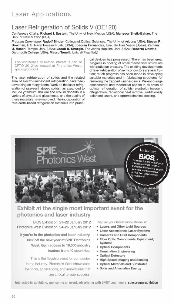
SPIE Photonics West 2012 Call for Papers · spie.org/lasecallpdf30
Laser App l icat ions
Laser Refrigeration of Solids V (OE120)Conference Chairs: Richard I. Epstein, The Univ. of New Mexico (USA); Mansoor Sheik-Bahae, The Univ. of New Mexico (USA)Program Committee: Rudolf Binder, College of Optical Sciences, The Univ. of Arizona (USA); Steven R. Bowman, U.S. Naval Research Lab. (USA); Joaquín Fernández, Univ. del País Vasco (Spain); Zameer U. Hasan, Temple Univ. (USA); Jacob B. Khurgin, The Johns Hopkins Univ. (USA); Roberto Onofrio, Dartmouth College (USA); Mauro Tonelli, Univ. di Pisa (Italy)
This conference of related interest is part of OPTO 2012 co-located at Photonics West, spie.org/optocall.
The laser refrigeration of solids and the related area of electroluminescent refrigeration have been advancing on many fronts. Work on the laser refrig-eration of rare-earth doped solids has expanded to include ytterbium, thulium and erbium dopants in a variety of crystal and glass hosts, and the quality of these materials have improved. The incorporation of rare-earth-based refrigeration materials into practi-
Exhibit at the single most important event for the photonics and laser industry
Display your latest innovations in:• Lasers and Other Light Sources• Laser Accessories, Laser Systems• Cameras and CCD Components• Fiber Optic Components, Equipment,
Systems• Optical Components• Illumination Engineering• Optical Detectors• High Speed Imaging and Sensing• Optical Materials and Substrates• Solar and Alternative Energy
BiOS Exhibition: 21–22 January 2012Photonics West Exhibition: 24–26 January 2012
If you’re in the photonics and laser industry,
kick off the new year at SPIE Photonics
West. Gain access to 19,000 industry
leaders from 40 countries.
This is the fl agship event for companies
in the industry. Photonics West showcases
the tools, applications, and innovations that
are critical to your success.
Including
Increase the impact of your Photonics West booth— Exhibit at the world’s largest international biomedical optics and biophotonics symposium!
Interested in exhibiting, sponsoring an event, advertising with SPIE? Learn more: spie.org/pwexhibition
cal devices has progressed. There has been great progress in cooling of small mechanical structures with radiation pressure. The exciting developments of laser refrigeration of semiconductors are near frui-tion; much progress has been made in developing suitable materials and in fabricating structures for removing the trapped luminescence. We encourage experimental and theoretical papers in all areas of optical refrigeration of solids, electroluminescent refrigeration, radiational heat removal, radiationally balanced lasers, and optomechanical cooling.
[email protected] · TEL: +1 360 676 3290 · +1 888 504 8171 31
Abst ract Submiss ion
By submitting an abstract, I agree to the following conditions:
An author or coauthor (including keynote, invited, oral, and poster presenters) will:• Register at the reduced author registration rate
(current SPIE Members receive an additional discount on the registration fee).
• Attend the meeting.• Make the presentation as scheduled in the pro-
gram.• Submit a full-length manuscript (6 pages mini-
mum) for publication in the SPIE Digital Library, Proceedings of SPIE, and CD-ROM compilations.
• Obtain funding for their registration fees, travel, and accommodations, independent of SPIE, through their sponsoring organizations.
• Ensure that all clearances, including government and company clearance, have been obtained to present and publish. If you are a DoD contractor in the USA, allow at least 60 days for clearance.
Submit an abstract and summary online at: spie.org/lasecallpdf• Abstracts should contain enough detail to clearly
convey the approach and the results of the re-search. Accepted abstracts will be published and made available at the meeting. Please submit a 250-word abstract for review.
• Please also submit a 100-word text summary suitable for early release. If accepted, this sum-mary text will be published prior to the meeting in the online or printed programs promoting the conference.
• If this research is working toward improvements in energy, sustainability, and conservation, enter GREEN PHOTONICS as your fi rst keyword in step 4 of the online submission wizard, and upload a 1-2 page summary in step 6. Abstracts accepted to the virtual Green Photonics Symposium will receive increased exposure at Photonics West and will be considered for Best Paper recognition. Note: 1-2 page upload not required if submission does not qualify as “Green Photonics.”
• Only original material should be submitted.• Abstracts should contain enough detail to clearly
convey the approach and the results of the re-search.
• Commercial papers, papers with no new research/development content, and papers where support-ing data or a technical description cannot be given for proprietary reasons will not be accepted for presentation in this conference.
• Please do not submit the same, or similar, ab-stracts to multiple conferences.
Review, Notifi cation, and Program Placement Information• To ensure a high-quality conference, all submis-
sions will be assessed by the Conference Chair/Editor for technical merit and suitability of content.
• Conference Chair/Editors reserve the right to reject for presentation any paper that does not meet content or presentation expectations.
• The contact author will receive notifi cation of ac-ceptance and presentation details by e-mail no later than 19 September 2011.
• Final placement in an oral or poster session is subject to the Chairs’ discretion.
Proceedings of SPIE and SPIE Digital Library Information• Conference Chair/Editors may require manuscript
revision before approving publication and reserve the right to reject for publication any paper that does not meet acceptable standards for a sci-entific publication. Conference Chair/Editors’ decisions on whether to allow publication of a manuscript is fi nal.
• Manuscript instructions are available from the “Author/Presenter Information” link on the confer-ence website.
• Authors must be authorized to transfer copyright of the manuscript to SPIE, or provide a suitable publication license.
• Only papers presented at the conference and received according to publication guidelines and timelines will be published in the conference Proceedings of SPIE and SPIE Digital Library.
• Published papers are indexed in leading scientifi c databases including INSPEC, Ei Compendex, Chemical Abstracts, International Aerospace Abstracts, ISI Index to Scientifi c and Techni-cal Proceedings and NASA Astrophysical Data System, and are searchable in the SPIE Digital Library. Full manuscripts are available to SPIE Digital Library subscribers worldwide..
Critical DatesAbstract Due Date: 11 July 2011Post-Meeting Manuscript Due Date: 19 December 2011
SPIE is the international society for optics and photonics founded in 1955 to advance light-based
technologies. Serving more than 188,000 constituents from 138 countries, the Society advances emerging
technologies through interdisciplinary information exchange, continuing education, publications, patent
precedent, and career and professional growth.
SPIE International HeadquartersP.O. Box 10, Bellingham, WA 98227-0010 USA Tel: +1 888 504 8171 or +1 360 676 3290, Fax: +1 360 647 1445 [email protected] • SPIE.org
SPIE Photonics West 2012 Call for Papers · spie.org/lasecallpdf32
Genera l In format ion
Helping engineers and scientists stay current and competitive
Find the answerSPIEDigitalLibrary.org
The international society for optics and photonics
VenueThe Moscone Center747 Howard StreetSan Francisco, CA 94103-3118 USASan Francisco is often called “Everybody’s Favorite City,” a title earned by its scenic beauty, cultural attractions, diverse communities, and world-class cuisine. Visitors rate the atmosphere and ambience as their top reason for visiting San Francisco. Mea-suring 49 square miles, this walkable city is dotted with landmarks like the Golden Gate Bridge, cable cars, and Alcatraz.
RegistrationSPIE Photonics West registration will be available October 2011
All participants, including invited speakers, con-tributed speakers, session chairs, co-chairs, and committee members, must pay a registration fee. Authors, coauthors, program committee members, and session chairs are accorded a reduced sympo-sium registration fee. Fee information for conferences, courses, a regis-tration form, and technical and general information will be available on the SPIE website in October 2011.
Hotel InformationOpening of the hotel reservation process for SPIE Photonics West 2012 is scheduled for the beginning of July 2011. SPIE will arrange special discounted hotel rates for SPIE attendees that will be available when housing opens. The website will be kept current with any updates.
Student Travel Contingency GrantsA limited number of SPIE contingency student travel grants will be awarded based on need. Applications must be received no later than 14 November 2011. Eligible applicants must present an accepted paper at this meeting. Offer applies to undergraduate/graduate students who are enrolled full-time and have not yet received their PhD.
Clearance InformationIf government and/or company clearance is required to present and publish your presenta tion, start the process now to ensure that you receive clearance if your paper is accepted.
Important News for All Visitors from Outside the United StatesFind important requirements for visiting the United States on the SPIE Photonics West website. There are new steps that ALL visitors to the United States need to follow.spie.org/lasecallpdf
Join the conversation—and get the latest news on SPIE Photonics West
spie.org/connect
#SPIEPW
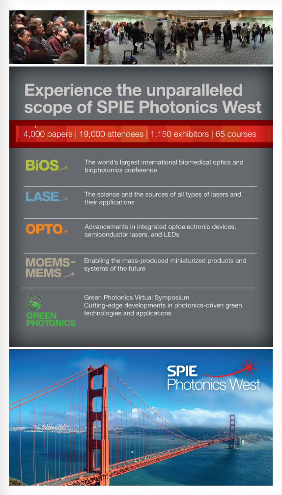
Experience the unparalleled scope of SPIE Photonics West4,000 papers | 19,000 attendees | 1,150 exhibitors | 65 courses
The world’s largest international biomedical optics and biophotonics conference
The science and the sources of all types of lasers and their applications
Advancements in integrated optoelectronic devices, semiconductor lasers, and LEDs
Enabling the mass-produced miniaturized products and systems of the future
Green Photonics Virtual Symposium Cutting-edge developments in photonics-driven green technologies and applications
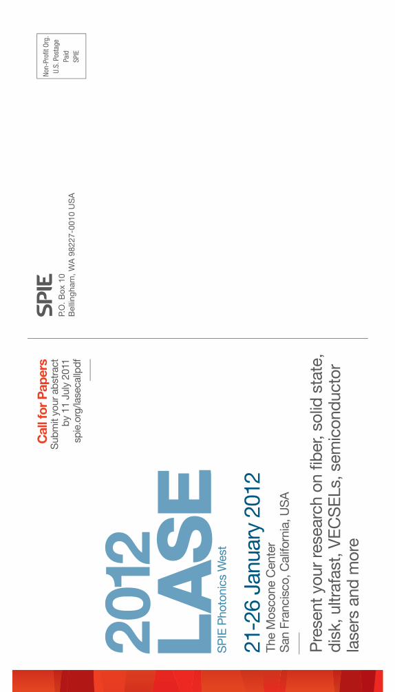
Non-
Profi
t Or
g.U.
S. P
osta
ge
Paid
SPIE
P.O
. Box
10
Bel
lingh
am, W
A 9
8227
-001
0 U
SA
21-2
6 Ja
nuar
y 20
12Th
e M
osco
ne C
ente
rS
an F
ranc
isco
, Cal
iforn
ia, U
SA
Sub
mit
your
abs
trac
tby
11
July
201
1
Cal
l for
Pap
ers
spie
.org
/lase
callp
df
Pre
sent
you
r res
earc
h on
fi be
r, so
lid s
tate
, di
sk, u
ltraf
ast,
VE
CS
ELs
, sem
icon
duct
or
lase
rs a
nd m
ore
SP
IE P
hoto
nics
Wes
t

![SPIE Photonics West 2009s-space.snu.ac.kr/bitstream/10371/7710/1/[2009_1]SPIE_김신애_2.pdf · 360 spie.org/pw · customerservice@spie.org · TEL: +1 360 676 3290 · +1 888 504](https://img.pdfslide.us/doc/110x75/5f5c356e3232607d4f7630cc/spie-photonics-west-2009s-spacesnuackrbitstream103717710120091spiee2pdf.jpg)