Embed Size (px)
Citation preview

Calibration and Dynamic Matching in Data Converters
Kenneth C. Dyer, John P. Keane1, and Stephen H. Lewis2
1 Keysight Technologies Inc., Santa Clara, CA USA
2 University of California, Davis, CA USA
1
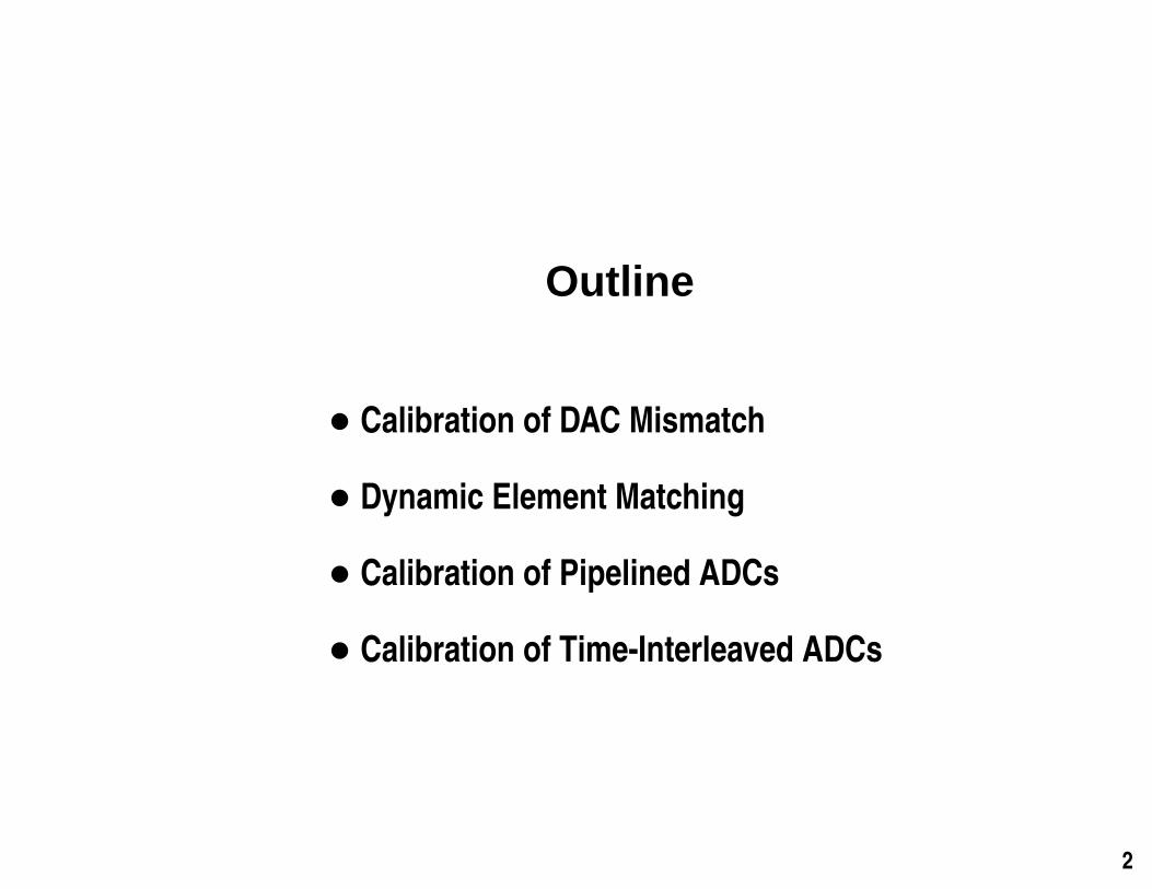
Outline
• Calibration of DAC Mismatch
• Dynamic Element Matching
• Calibration of Pipelined ADCs
• Calibration of Time-Interleaved ADCs
2
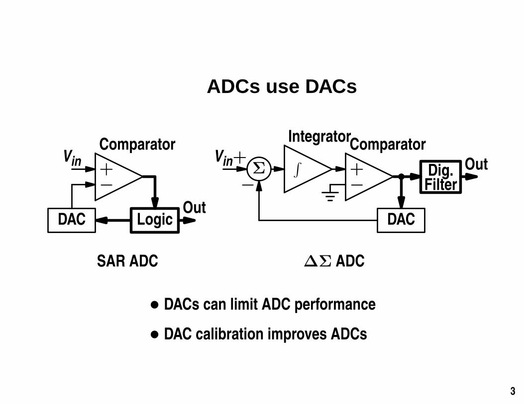
ADCs use DACs
Vin +
Comparator
LogicOut
DAC
−
SAR ADC
Vin+ Σ
Integrator
∫+−
Comparator
DAC
Dig.Filter
Out
−
∆Σ ADC
• DACs can limit ADC performance
• DAC calibration improves ADCs
3
Laser Trimming an R-2R Ladder DACIout
2RN−2
RN−1 ≈ R RN ≈ R
IN−2
BN−2
2RN−1
IN−1
BN−1
2RN
IN
BN
IT
2R
Cal
• Holloway and Norton, ISSCC76 [1]
• If IN−1 < IN + IT , trim RN
• If IN−1 > IN + IT , trim 2RN−1
• Single-pass trim (start on right and move to left) improves linearity
4
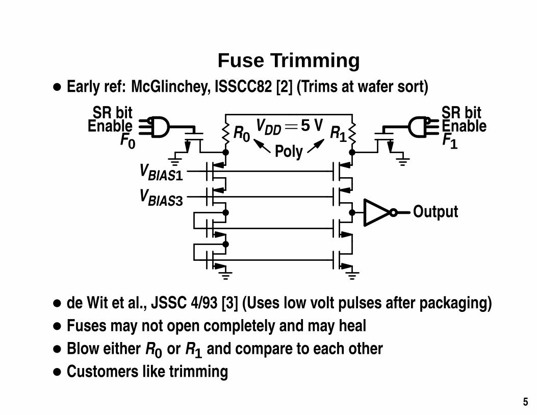
Fuse Trimming• Early ref: McGlinchey, ISSCC82 [2] (Trims at wafer sort)
R0
VBIAS1
VBIAS3
SR bitEnableF0
VDD=5 V R1Poly
Output
SR bitEnableF1
• de Wit et al., JSSC 4/93 [3] (Uses low volt pulses after packaging)
• Fuses may not open completely and may heal
• Blow either R0 or R1 and compare to each other
• Customers like trimming
5
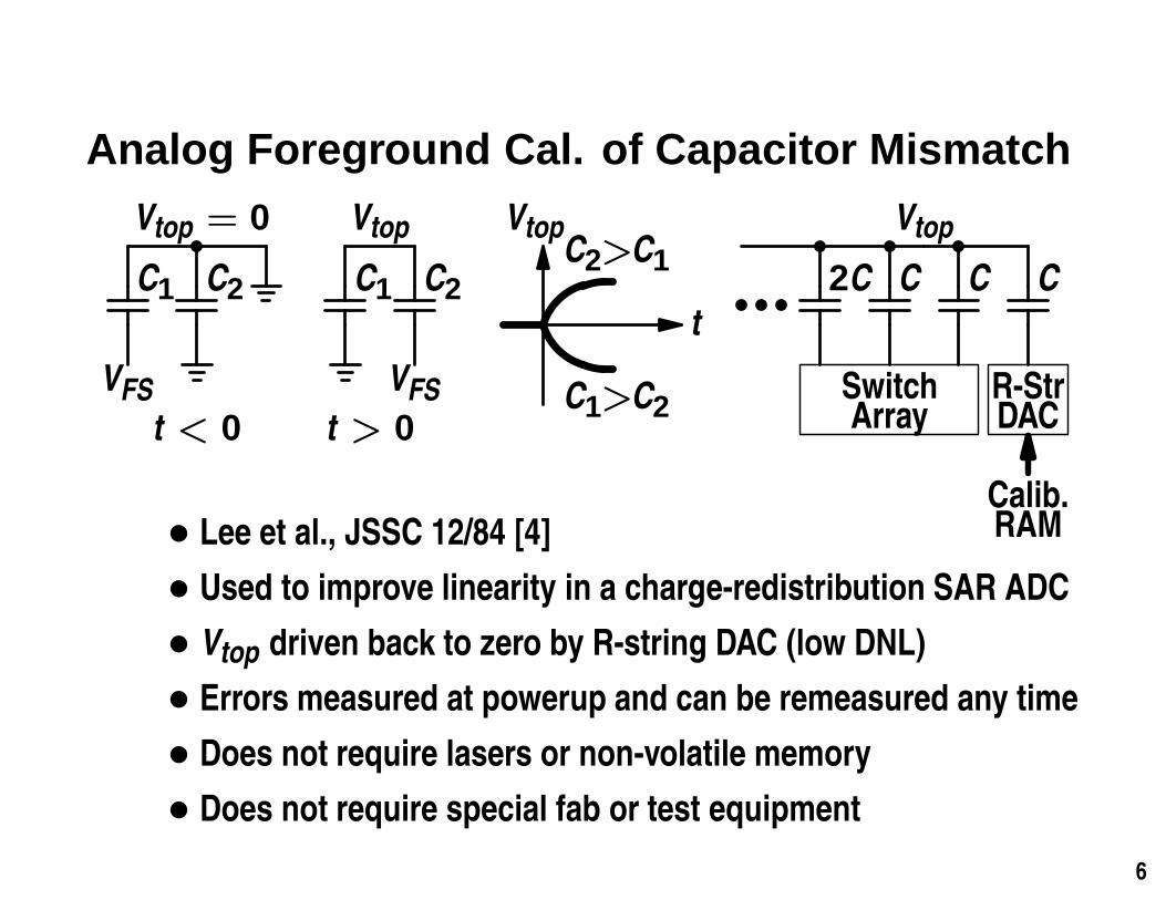
Analog Foreground Cal. of Capacitor Mismatch
C1
VFS
Vtop = 0
C2
t < 0
C1
Vtop
C2
VFSt > 0
t
VtopC2>C1
C1>C2
2C C
Vtop
C C
SwitchArray
R-StrDAC
Calib.RAM• Lee et al., JSSC 12/84 [4]
• Used to improve linearity in a charge-redistribution SAR ADC
• Vtop driven back to zero by R-string DAC (low DNL)
• Errors measured at powerup and can be remeasured any time
• Does not require lasers or non-volatile memory
• Does not require special fab or test equipment
6
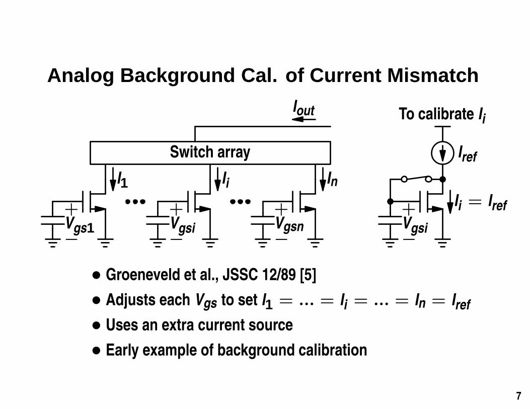
Analog Background Cal. of Current Mismatch
+Vgs1−
I1
+Vgsi−
Ii
+Vgsn−
In
Switch array
Iout To calibrate Ii
Ii = Iref
Iref
+Vgsi−
• Groeneveld et al., JSSC 12/89 [5]
• Adjusts each Vgs to set I1 = ... = Ii = ... = In = Iref
• Uses an extra current source
• Early example of background calibration
7
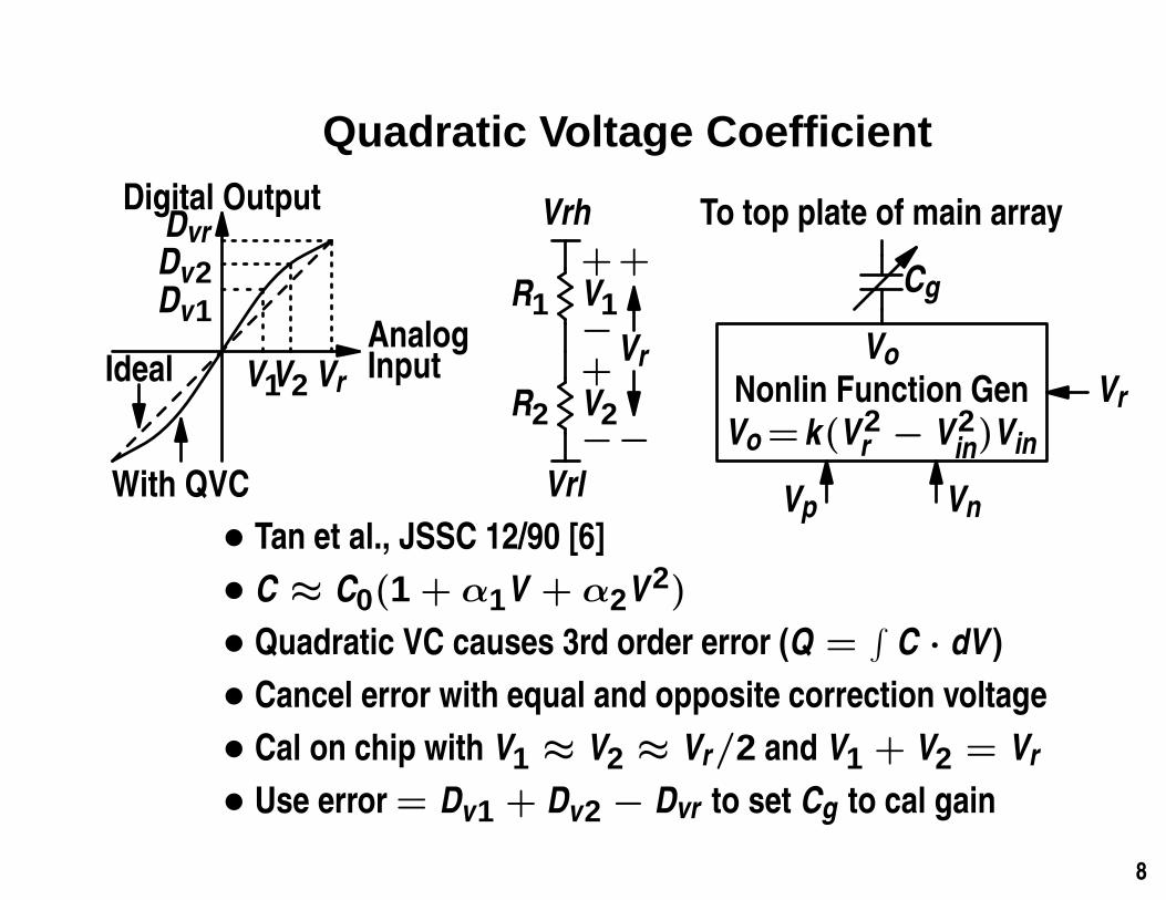
Quadratic Voltage Coefficient
AnalogInput
Digital Output
Ideal
With QVC
V1
Dv1
V2
Dv2
Vr
DvrVrh
R1
R2
Vrl
+V1−+V2−
Vr
+
−
To top plate of main array
Cg
VoNonlin Function GenVo=k(V
2r − V2
in)Vin
Vr
VnVp• Tan et al., JSSC 12/90 [6]
• C ≈ C0(1 + α1V + α2V2)
• Quadratic VC causes 3rd order error (Q =∫C · dV )
• Cancel error with equal and opposite correction voltage
• Cal on chip with V1 ≈ V2 ≈ Vr/2 and V1 + V2 = Vr
• Use error= Dv1 + Dv2 − Dvr to set Cg to cal gain
8
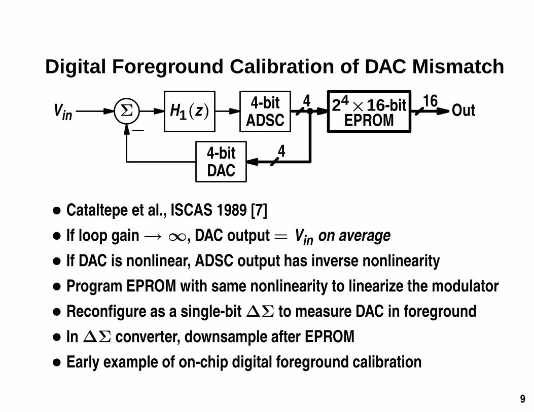
Digital Foreground Calibration of DAC Mismatch
Vin Σ H1(z)4-bitADSC
24×16-bitEPROM
Out
4-bitDAC
−
4 16
4
• Cataltepe et al., ISCAS 1989 [7]
• If loop gain→ ∞, DAC output= Vin on average
• If DAC is nonlinear, ADSC output has inverse nonlinearity
• Program EPROM with same nonlinearity to linearize the modulator
• Reconfigure as a single-bit∆Σ to measure DAC in foreground
• In∆Σ converter, downsample after EPROM
• Early example of on-chip digital foreground calibration
9
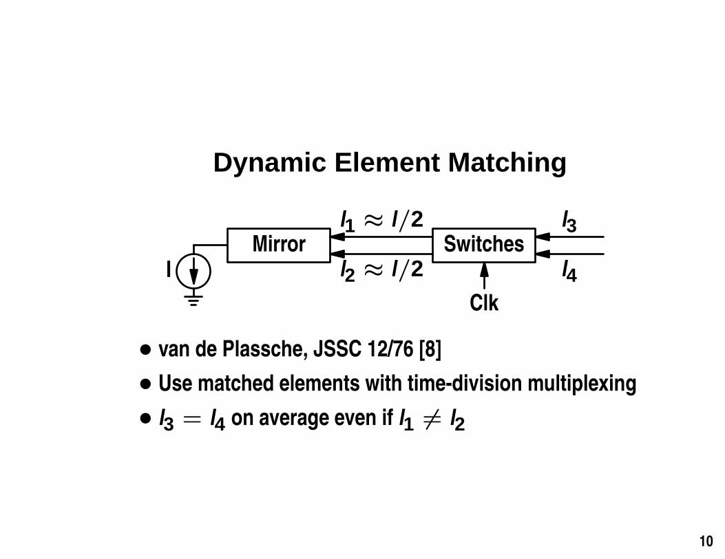
Dynamic Element Matching
IMirror
I1 ≈ I/2
I2 ≈ I/2Switches
I3
I4
Clk
• van de Plassche, JSSC 12/76 [8]
• Use matched elements with time-division multiplexing
• I3 = I4 on average even if I1 6= I2
10
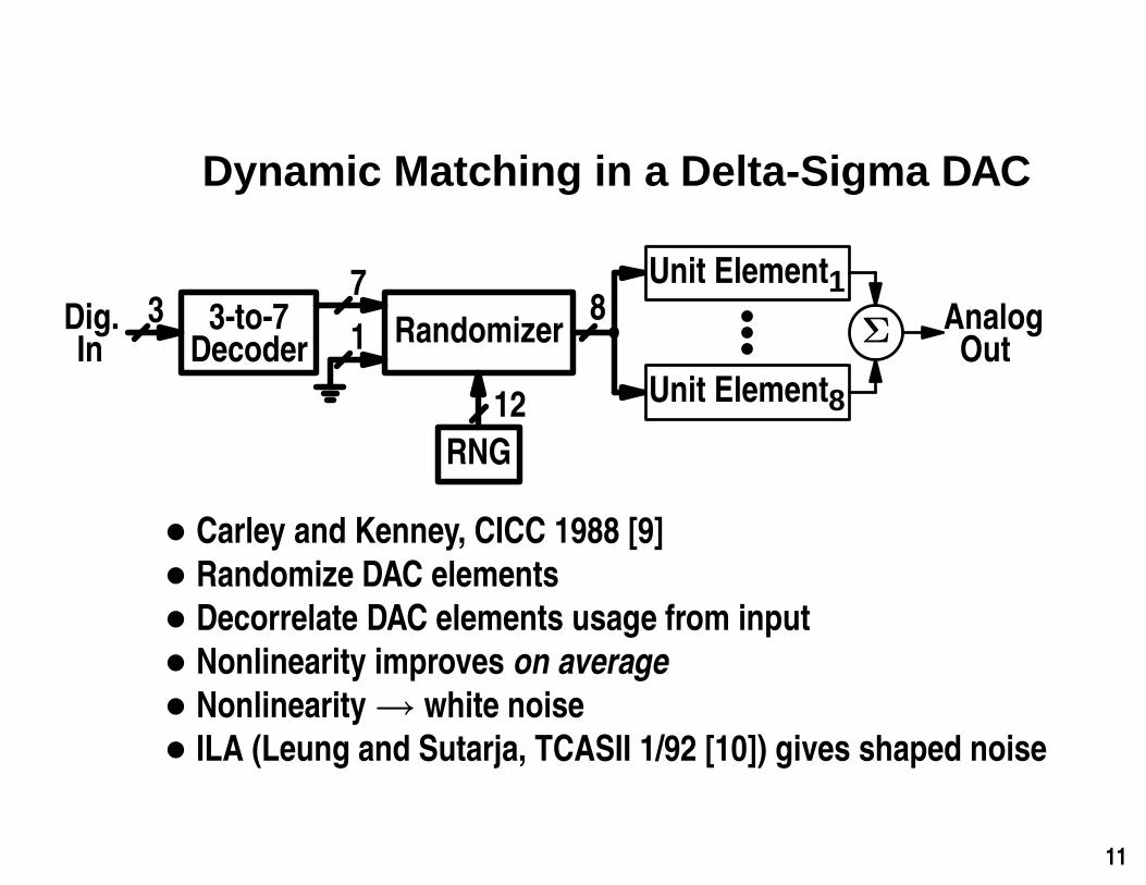
Dynamic Matching in a Delta-Sigma DAC
Dig.In3 3-to-7Decoder
7
Randomizer
Unit Element1
Unit Element8
8Σ Analog
Out1
RNG
12
• Carley and Kenney, CICC 1988 [9]
• Randomize DAC elements
• Decorrelate DAC elements usage from input
• Nonlinearity improves on average
• Nonlinearity→ white noise
• ILA (Leung and Sutarja, TCASII 1/92 [10]) gives shaped noise
11
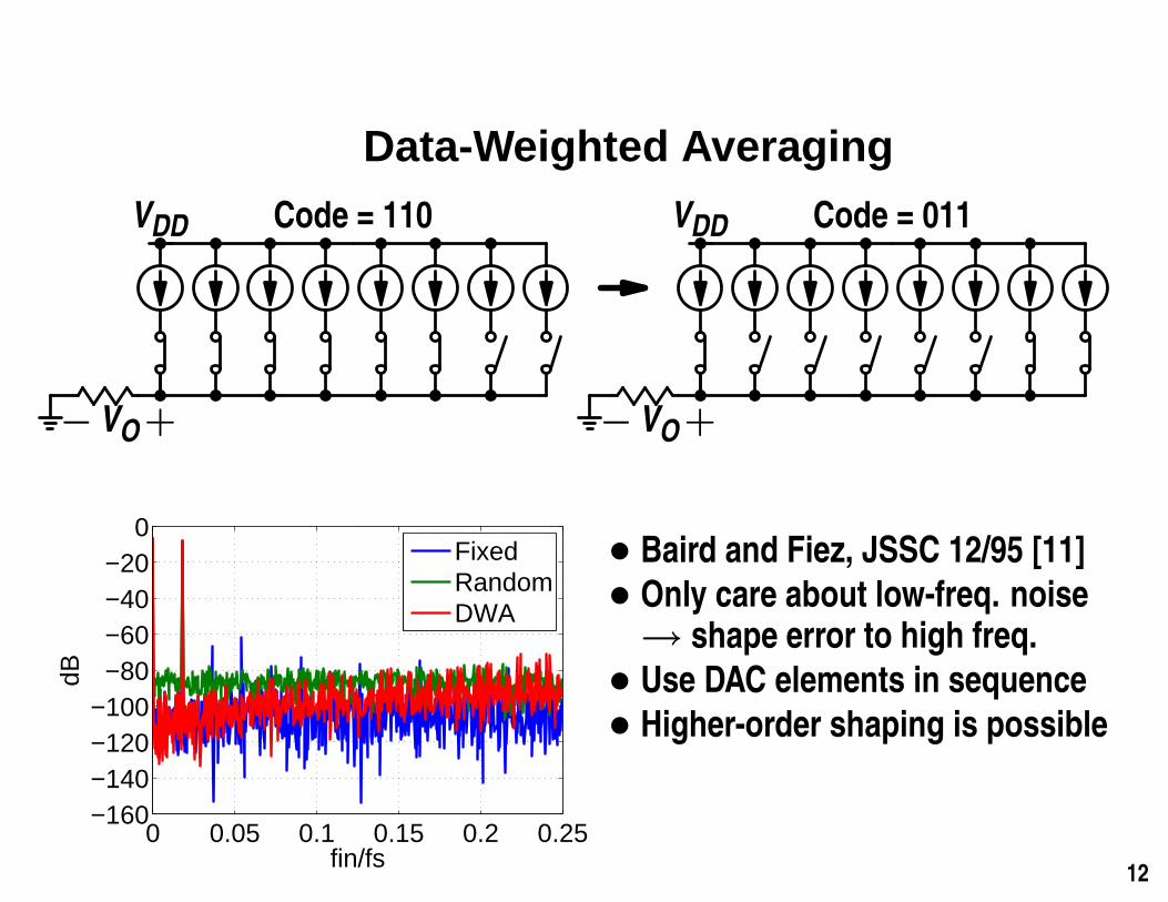
Data-Weighted Averaging
VDD
+VO−
Code = 110 VDD
+VO−
Code = 011
0 0.05 0.1 0.15 0.2 0.25−160−140−120−100−80−60−40−20
0
fin/fs
dB
FixedRandomDWA
• Baird and Fiez, JSSC 12/95 [11]
• Only care about low-freq. noise→ shape error to high freq.
• Use DAC elements in sequence
• Higher-order shaping is possible
12
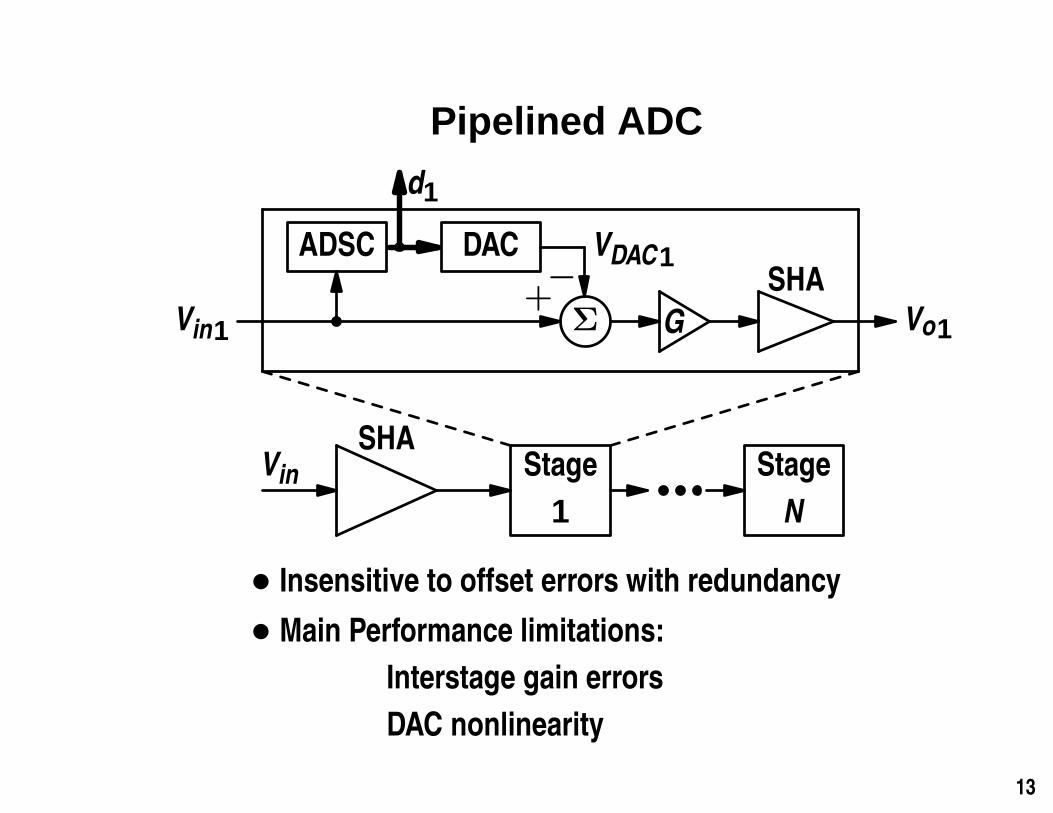
Pipelined ADC
VinSHA
Stage
1
Σ G
SHA
Vo1Vin1
ADSC DAC
d1
−VDAC1
Stage
N
+
• Insensitive to offset errors with redundancy
• Main Performance limitations:
Interstage gain errors
DAC nonlinearity
13
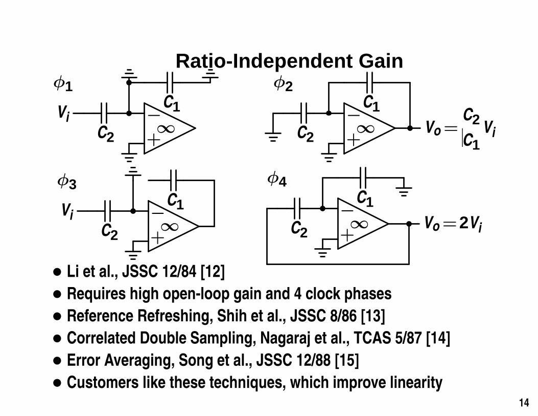
Ratio-Independent Gain
Vi
φ1
C2
−
+∞
C1
C2
−
+
φ2
∞
C1
Vo=C2
C1Vi
Vi
φ3
C2
−
+∞
C1
C2
−
+
φ4
∞
C1
Vo=2Vi
• Li et al., JSSC 12/84 [12]
• Requires high open-loop gain and 4 clock phases
• Reference Refreshing, Shih et al., JSSC 8/86 [13]
• Correlated Double Sampling, Nagaraj et al., TCAS 5/87 [14]
• Error Averaging, Song et al., JSSC 12/88 [15]
• Customers like these techniques, which improve linearity14
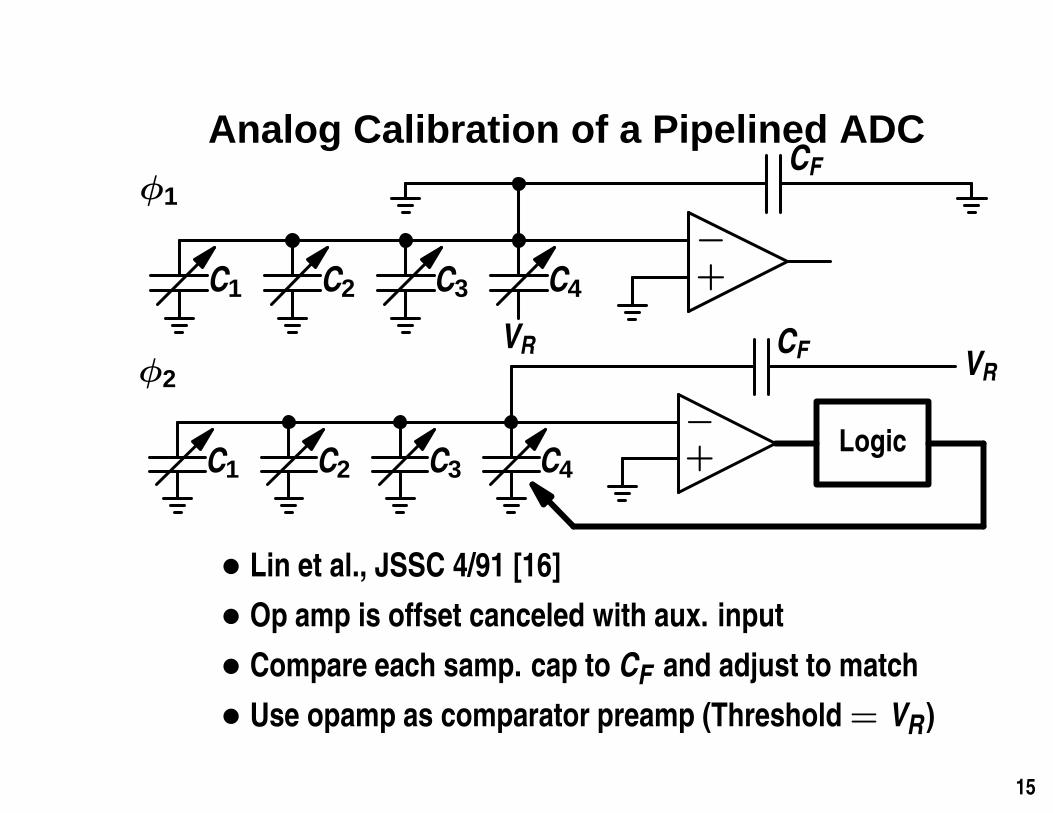
Analog Calibration of a Pipelined ADCφ1
C1 C2 C3 C4
VR
−+
CF
φ2
C1 C2 C3 C4
−+
Logic
CFVR
• Lin et al., JSSC 4/91 [16]
• Op amp is offset canceled with aux. input
• Compare each samp. cap to CF and adjust to match
• Use opamp as comparator preamp (Threshold= VR )
15
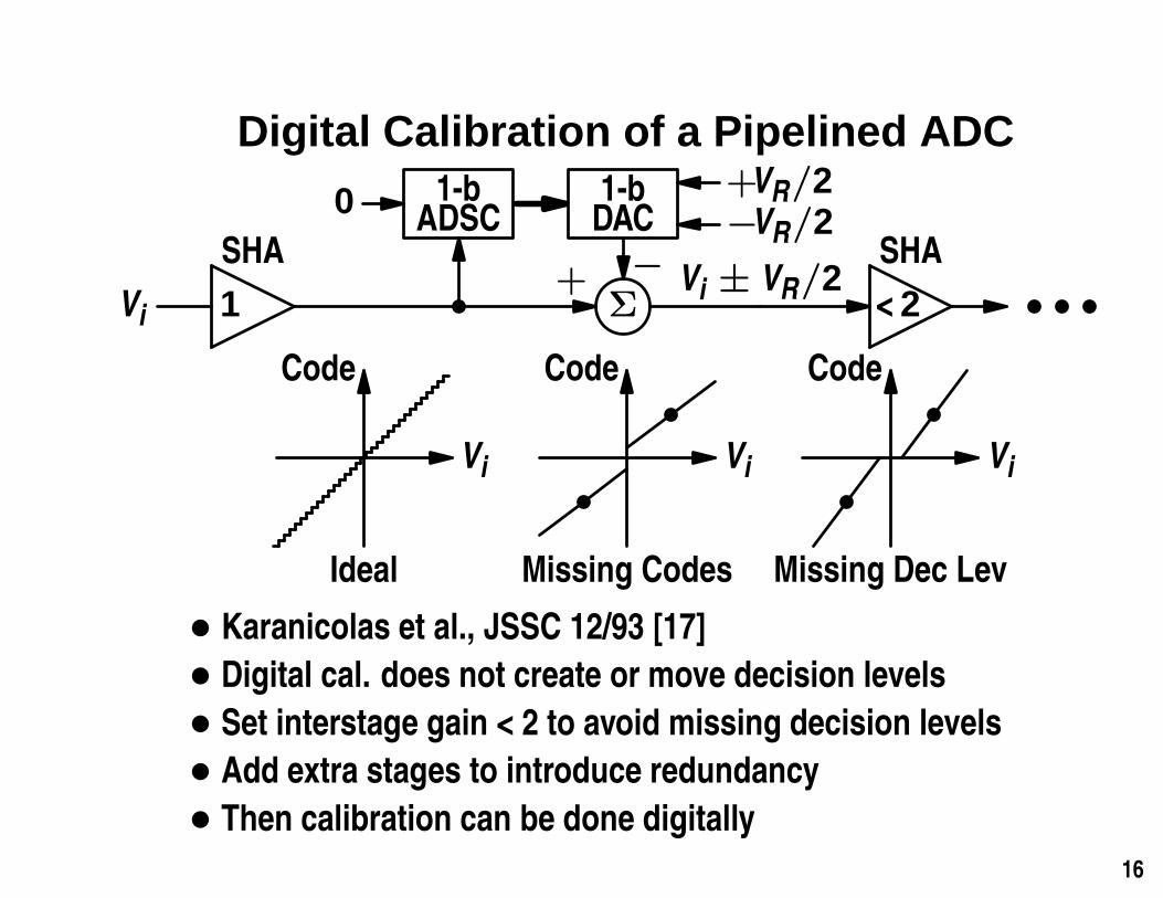
Digital Calibration of a Pipelined ADC
Vi
SHA
1
1-bADSC0 1-b
DAC+VR/2−VR/2
−Σ
+ Vi ± VR/2SHA
< 2
Vi
Ideal
Code
Vi
Missing Codes
Code
Vi
Missing Dec Lev
Code
• Karanicolas et al., JSSC 12/93 [17]
• Digital cal. does not create or move decision levels
• Set interstage gain < 2 to avoid missing decision levels
• Add extra stages to introduce redundancy
• Then calibration can be done digitally
16
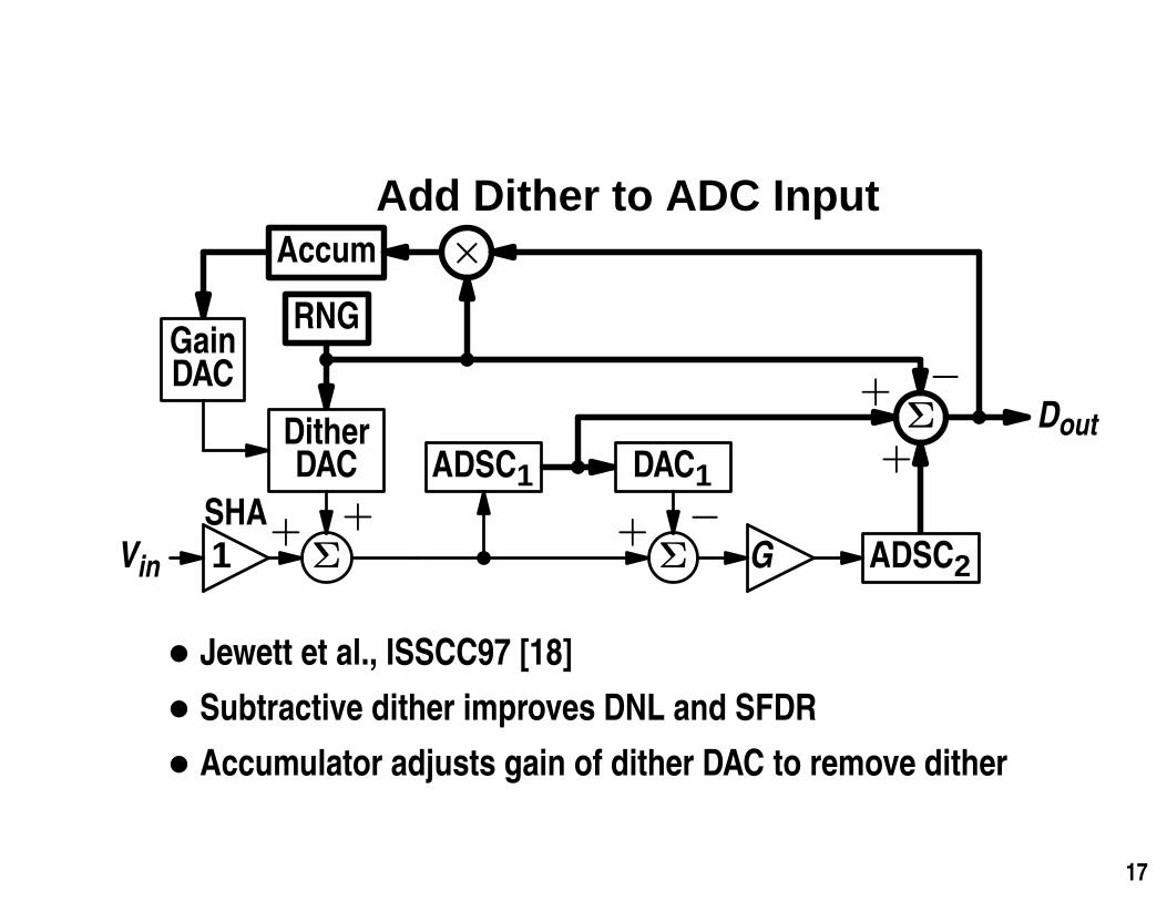
Add Dither to ADC Input
Vin 1SHA+
Σ+
Σ G ADSC2
ADSC1 DAC1−
+Σ
+Dout
×Accum
DACGain
RNG
DACDither
+
−
• Jewett et al., ISSCC97 [18]
• Subtractive dither improves DNL and SFDR
• Accumulator adjusts gain of dither DAC to remove dither
17
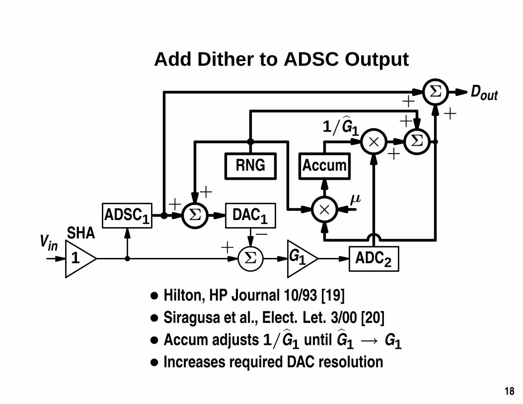
Add Dither to ADSC Output
1
SHA+
Σ G1 ADC2
Vin
ADSC1+
Σ DAC1−
+Σ Dout
RNG
+
+
×+
Σ
+
×
Accum
1/G1
µ
• Hilton, HP Journal 10/93 [19]
• Siragusa et al., Elect. Let. 3/00 [20]
• Accum adjusts 1/G1 until G1 → G1• Increases required DAC resolution
18
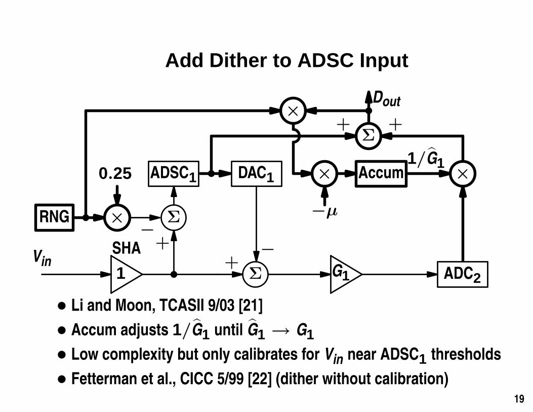
Add Dither to ADSC Input
1
SHA+
Σ G1 ADC2
Vin+
Σ
ADSC1 DAC1
−
+Σ
Dout×
× Accum1/G1
−µRNG ×−
0.25 ×
+
• Li and Moon, TCASII 9/03 [21]
• Accum adjusts 1/G1 until G1 → G1• Low complexity but only calibrates for Vin near ADSC1 thresholds
• Fetterman et al., CICC 5/99 [22] (dither without calibration)19
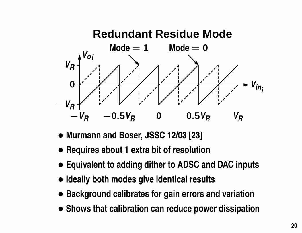
Redundant Residue Mode
Voi
−VR
Vini
−0.5VR 0
Mode= 0
0.5VR VR
VR
0
−VR
Mode= 1
• Murmann and Boser, JSSC 12/03 [23]
• Requires about 1 extra bit of resolution
• Equivalent to adding dither to ADSC and DAC inputs
• Ideally both modes give identical results
• Background calibrates for gain errors and variation
• Shows that calibration can reduce power dissipation
20
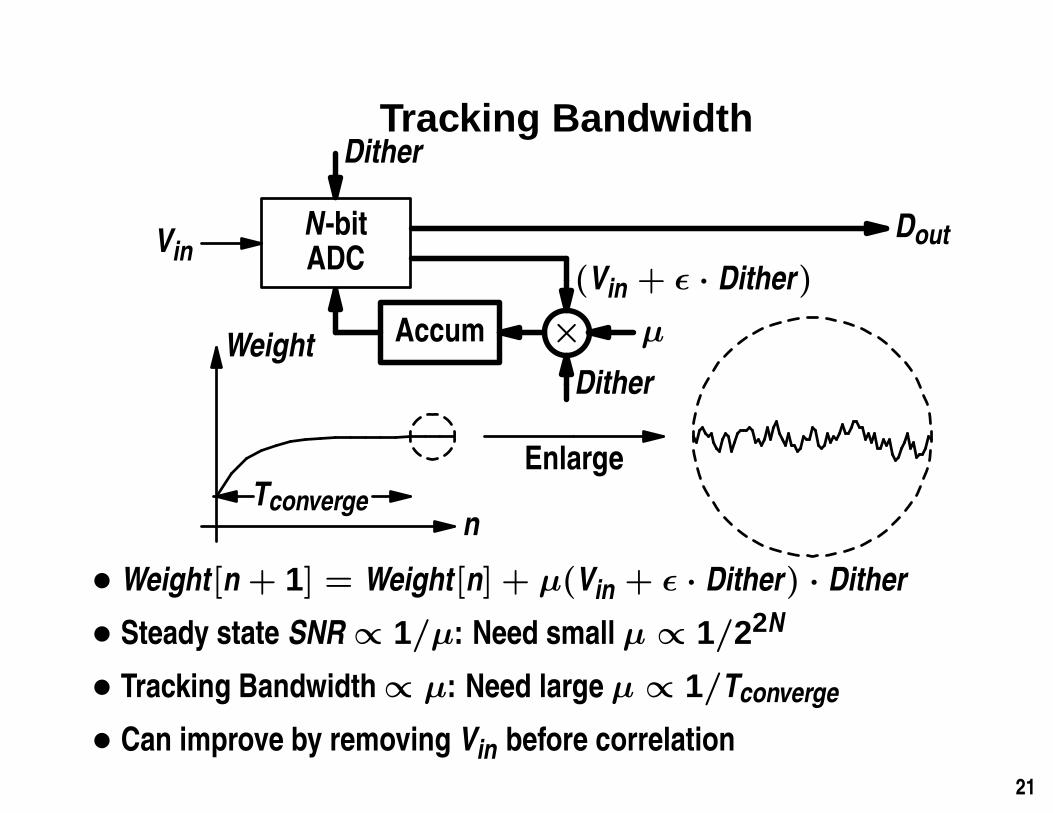
Tracking Bandwidth
VinN-bitADC
Dout
(Vin + ǫ · Dither)
× µAccum
Dither
Dither
Weight
n
EnlargeTconverge
• Weight[n + 1] = Weight[n] + µ(Vin + ǫ · Dither) · Dither
• Steady state SNR ∝ 1/µ: Need small µ ∝ 1/22N
• Tracking Bandwidth∝ µ: Need large µ ∝ 1/Tconverge
• Can improve by removing Vin before correlation
21
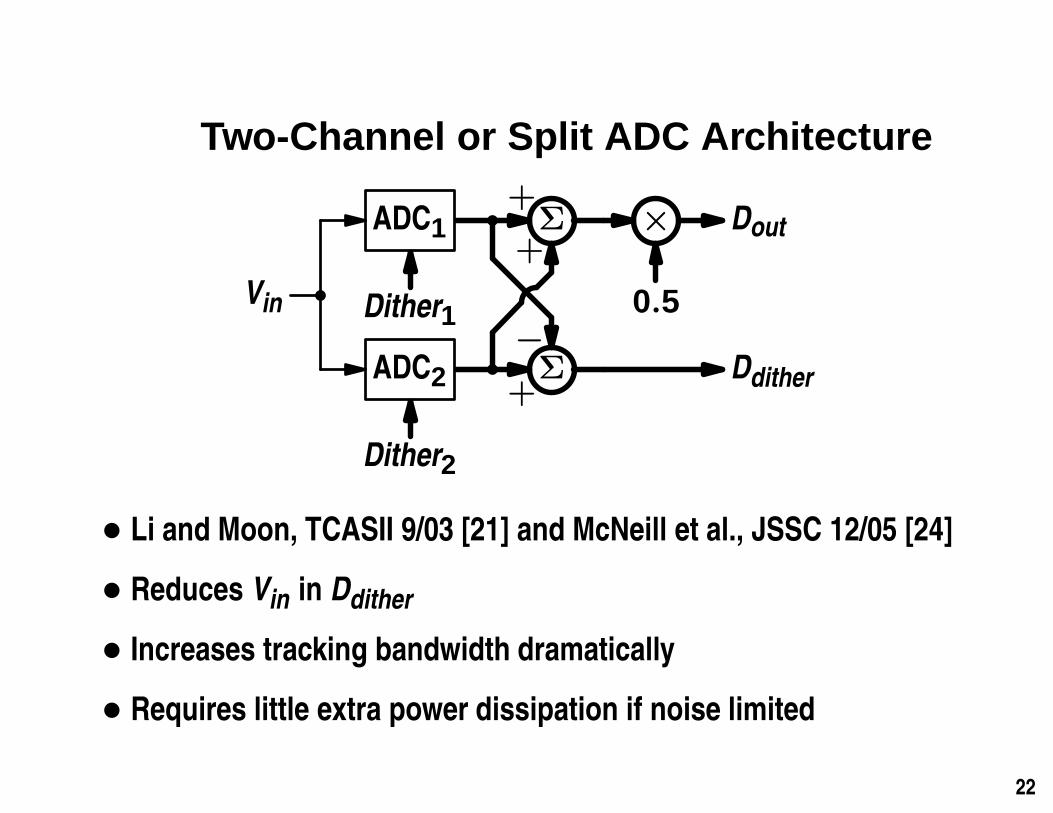
Two-Channel or Split ADC Architecture
Vin
ADC1
Dither1
+Σ × Dout
0.5
ADC2
Dither2
+Σ Ddither
−
+
• Li and Moon, TCASII 9/03 [21] and McNeill et al., JSSC 12/05 [24]
• Reduces Vin in Ddither
• Increases tracking bandwidth dramatically
• Requires little extra power dissipation if noise limited
22
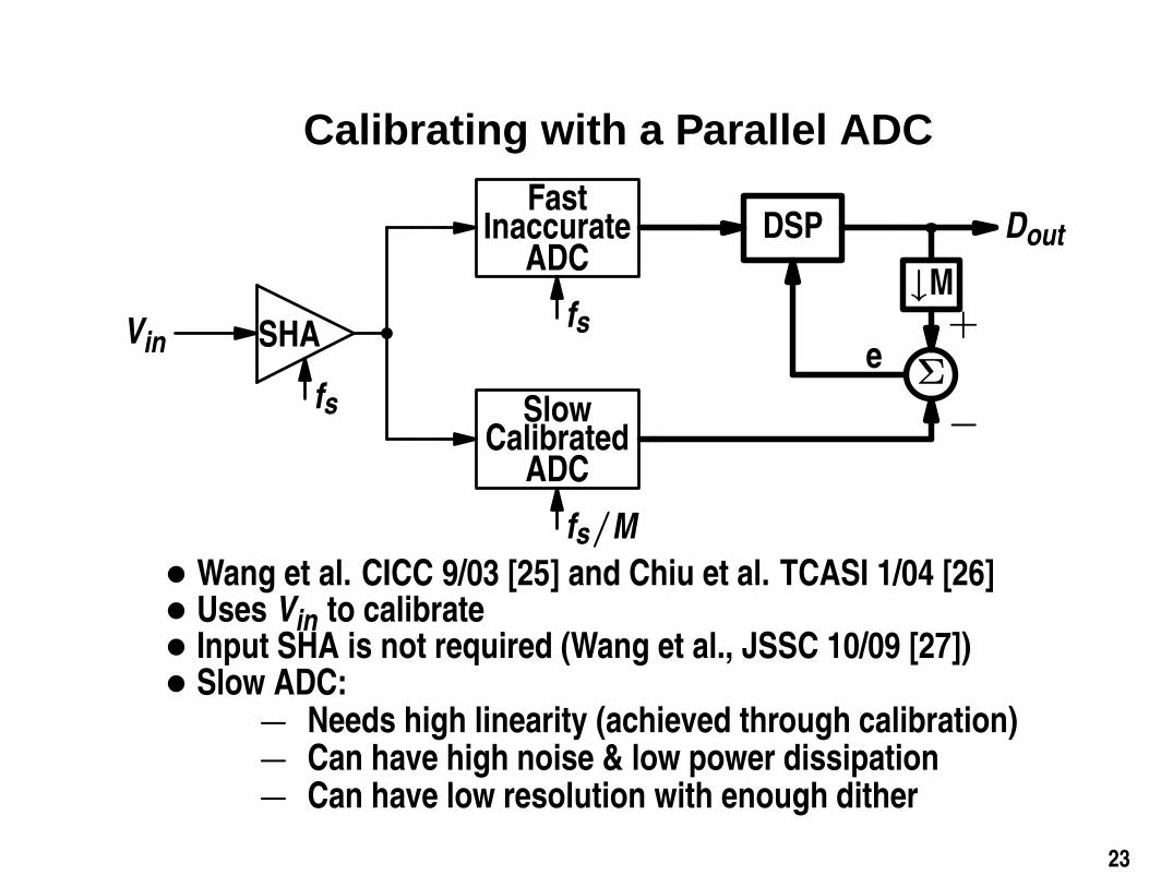
Calibrating with a Parallel ADC
SHA
FastInaccurateADC
fs
DSP
↓M
Σe+
−SlowCalibratedADC
fs/M
Dout
Vin
fs
• Wang et al. CICC 9/03 [25] and Chiu et al. TCASI 1/04 [26]• Uses Vin to calibrate• Input SHA is not required (Wang et al., JSSC 10/09 [27])• Slow ADC:
− Needs high linearity (achieved through calibration)− Can have high noise & low power dissipation− Can have low resolution with enough dither
23
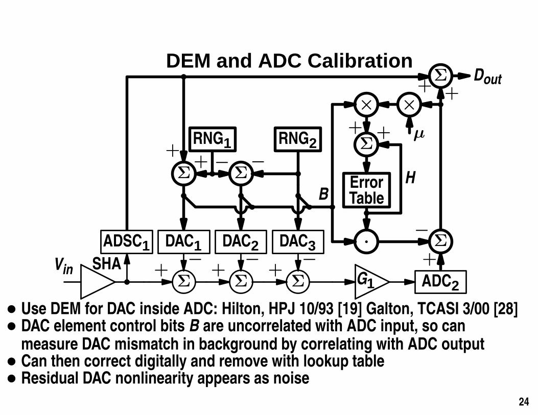
DEM and ADC Calibration
SHA +Σ
+Σ
+Σ G1 ADC2
+Vin
ADSC1 DAC1 DAC2 DAC3− − −
+
Σ
RNG1+ −
Σ
RNG2−
B
×
+Σ
ErrorTable
·−
Σ
+Σ Dout
×
µ
H
+
+
• Use DEM for DAC inside ADC: Hilton, HPJ 10/93 [19] Galton, TCASI 3/00 [28]• DAC element control bits B are uncorrelated with ADC input, so canmeasure DAC mismatch in background by correlating with ADC output
• Can then correct digitally and remove with lookup table• Residual DAC nonlinearity appears as noise
24
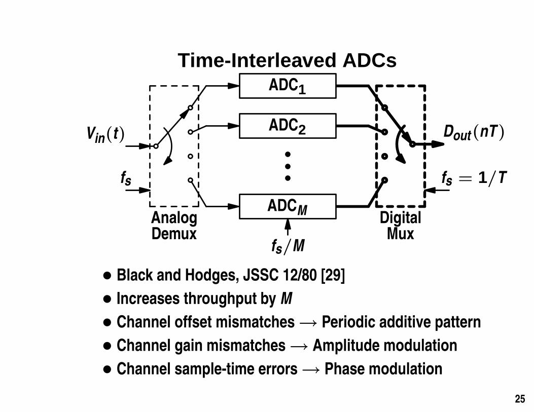
Time-Interleaved ADCs
Vin(t)
AnalogDemux
fs
ADC1
ADC2
ADCMDigitalMux
fs/M
fs = 1/T
Dout(nT)
• Black and Hodges, JSSC 12/80 [29]
• Increases throughput by M
• Channel offset mismatches→ Periodic additive pattern
• Channel gain mismatches→ Amplitude modulation
• Channel sample-time errors→ Phase modulation
25
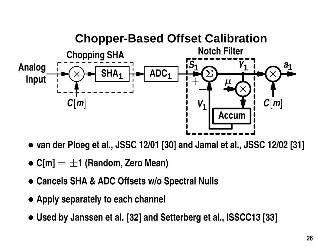
Chopper-Based Offset Calibration
×
C[m]
SHA1 ADC1Analog
Input
Chopping SHAS1
+Σ
Y1×
C[m]
a1
Notch Filter
×
Accum
−
V1
µ
• van der Ploeg et al., JSSC 12/01 [30] and Jamal et al., JSSC 12/02 [31]
• C[m]= ±1 (Random, Zero Mean)
• Cancels SHA & ADC Offsets w/o Spectral Nulls
• Apply separately to each channel
• Used by Janssen et al. [32] and Setterberg et al., ISSCC13 [33]
26
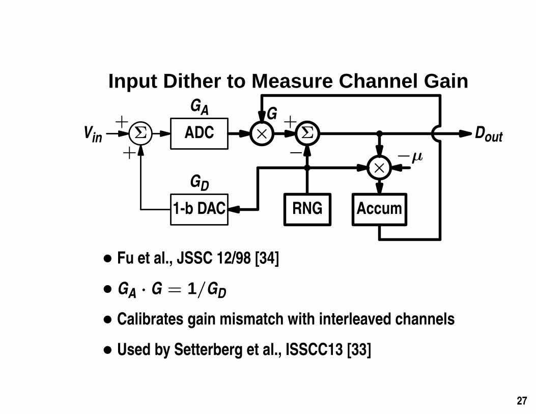
Input Dither to Measure Channel Gain
Vin+
Σ ADC ×+
Σ Dout
GA
RNG
−
1-b DAC
+
GD×
−µ
Accum
G
• Fu et al., JSSC 12/98 [34]
• GA · G = 1/GD
• Calibrates gain mismatch with interleaved channels
• Used by Setterberg et al., ISSCC13 [33]
27
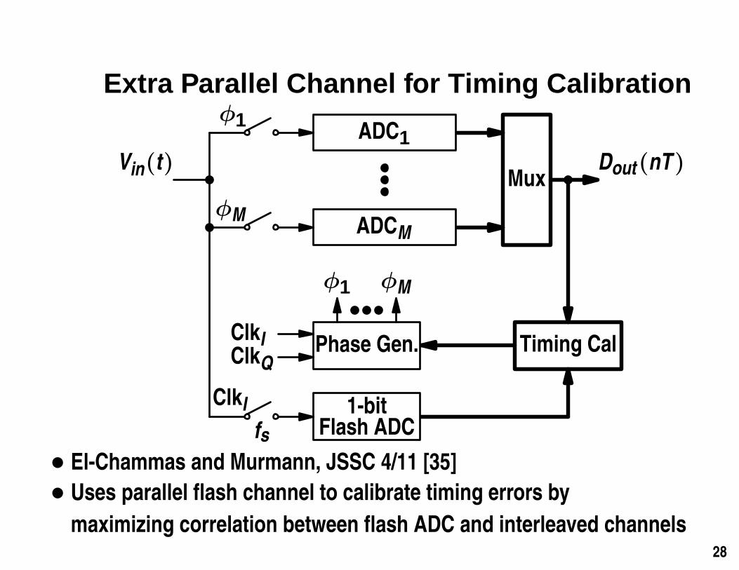
Extra Parallel Channel for Timing Calibration
Vin(t)
φ1ADC1
φMADCM
MuxDout(nT)
Timing CalPhase Gen.ClkIClkQ
φ1 φM
ClkIfs
1-bitFlash ADC
• El-Chammas and Murmann, JSSC 4/11 [35]
• Uses parallel flash channel to calibrate timing errors by
maximizing correlation between flash ADC and interleaved channels28
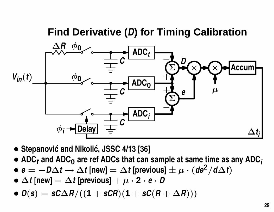
Find Derivative ( D) for Timing Calibration
Vin(t)
∆R φ0
CADCt
φ0
CADC0
CADCi
−ΣD
× ×
µ
Accum
∆tiDelayφi
+
+Σe
−
• Stepanovic and Nikolic, JSSC 4/13 [36]
• ADCt and ADC0 are ref ADCs that can sample at same time as any ADCi• e = −D∆t→ ∆t [new]= ∆t [previous]± µ · (de2/d∆t)• ∆t [new]= ∆t [previous]+ µ · 2 · e · D
• D(s) = sC∆R/((1 + sCR)(1 + sC(R + ∆R)))
29
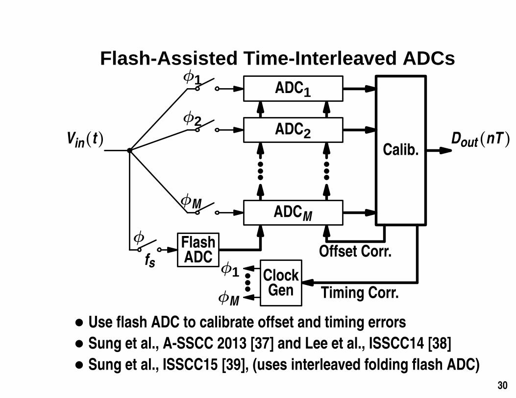
Flash-Assisted Time-Interleaved ADCs
Vin(t)
φ1ADC1
φ2ADC2
φMADCM
Calib.Dout(nT)
φ
fs
FlashADC Offset Corr.
Timing Corr.ClockGen
φ1
φM
• Use flash ADC to calibrate offset and timing errors
• Sung et al., A-SSCC 2013 [37] and Lee et al., ISSCC14 [38]
• Sung et al., ISSCC15 [39], (uses interleaved folding flash ADC)30
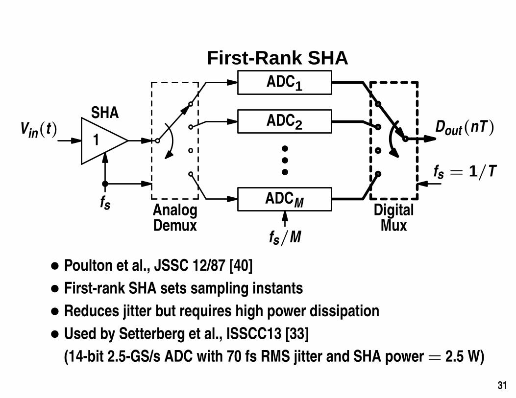
First-Rank SHA
Vin(t)
fs
SHA
1
AnalogDemux
ADC1
ADC2
ADCMDigitalMux
fs/M
fs = 1/T
Dout(nT)
• Poulton et al., JSSC 12/87 [40]
• First-rank SHA sets sampling instants
• Reduces jitter but requires high power dissipation
• Used by Setterberg et al., ISSCC13 [33]
(14-bit 2.5-GS/s ADC with 70 fs RMS jitter and SHA power= 2.5 W)
31
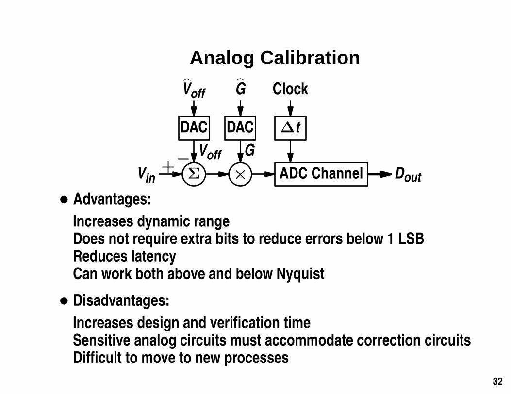
Analog Calibration
Vin+ Σ × ADC Channel Dout
Voff
DAC
−Voff
G
DAC
G
Clock
∆t
• Advantages:
Increases dynamic rangeDoes not require extra bits to reduce errors below 1 LSBReduces latencyCan work both above and below Nyquist
• Disadvantages:
Increases design and verification timeSensitive analog circuits must accommodate correction circuitsDifficult to move to new processes
32
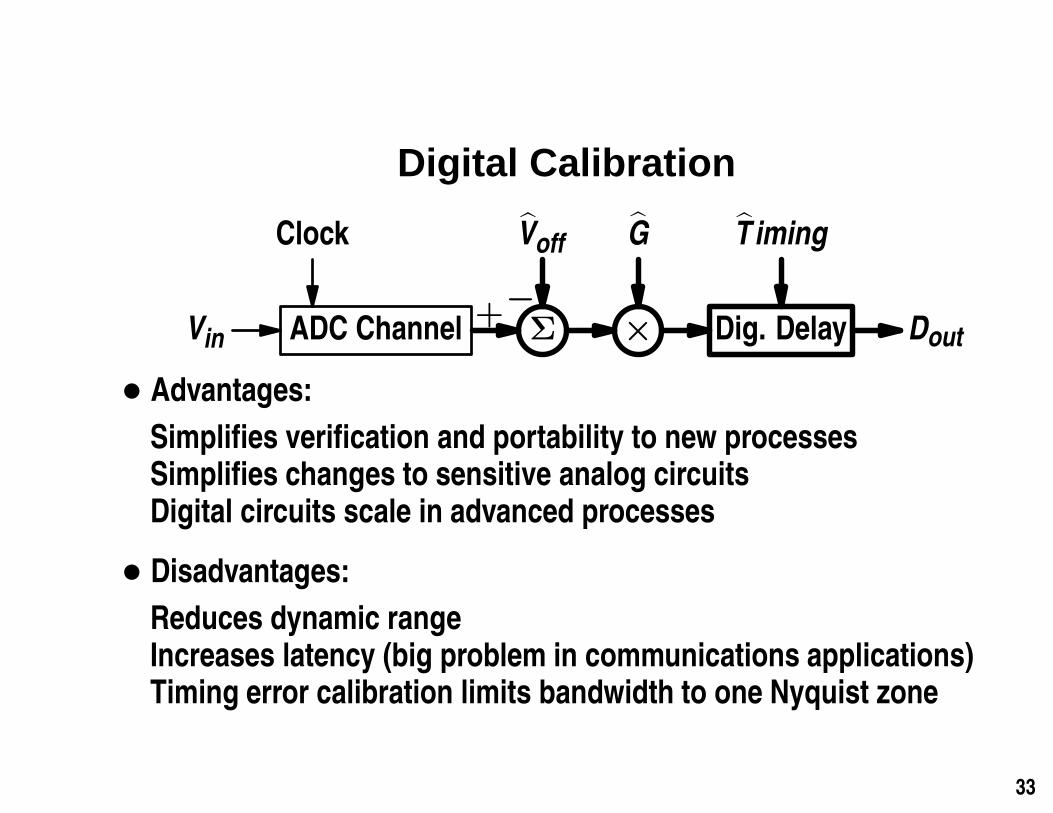
Digital Calibration
Vin ADC Channel+ Σ × Dig. Delay Dout
Clock Voff
−
G T iming
• Advantages:
Simplifies verification and portability to new processesSimplifies changes to sensitive analog circuitsDigital circuits scale in advanced processes
• Disadvantages:
Reduces dynamic rangeIncreases latency (big problem in communications applications)Timing error calibration limits bandwidth to one Nyquist zone
33
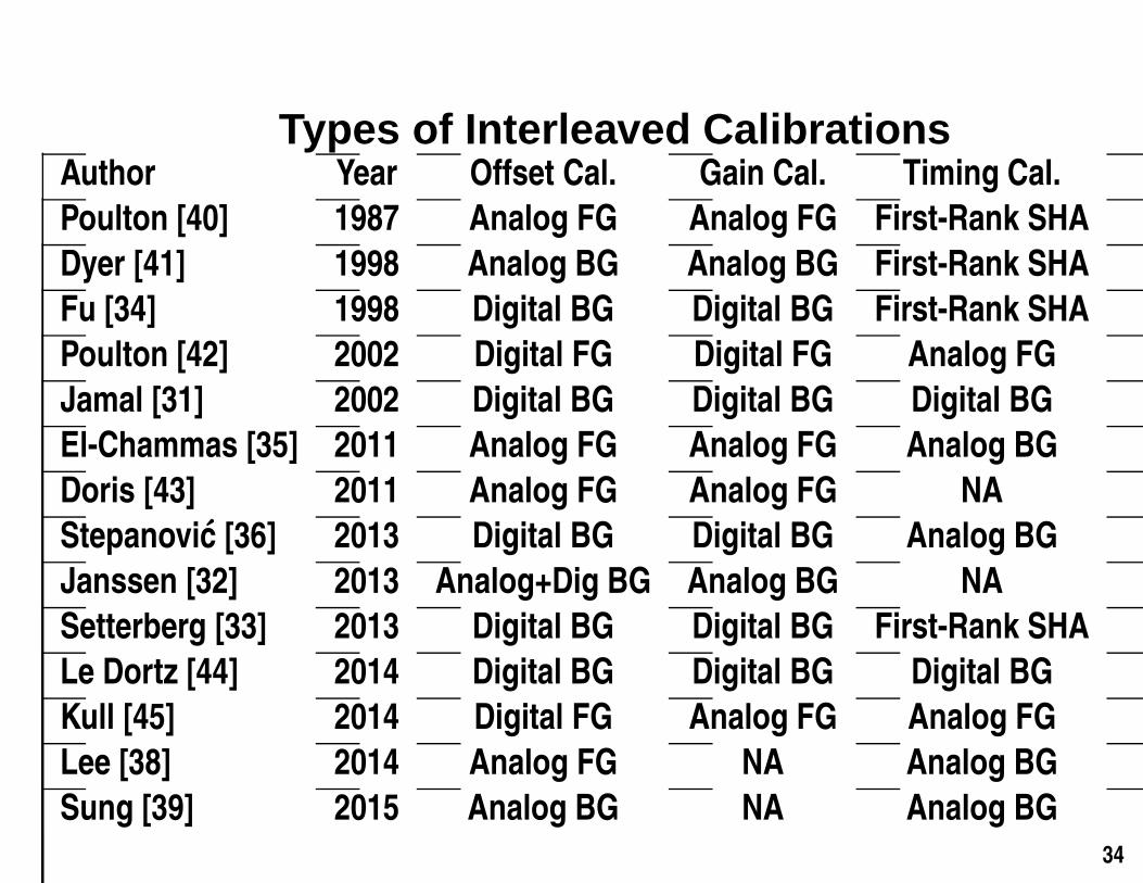
Types of Interleaved CalibrationsAuthor Year Offset Cal. Gain Cal. Timing Cal.
Poulton [40] 1987 Analog FG Analog FG First-Rank SHA
Dyer [41] 1998 Analog BG Analog BG First-Rank SHA
Fu [34] 1998 Digital BG Digital BG First-Rank SHA
Poulton [42] 2002 Digital FG Digital FG Analog FG
Jamal [31] 2002 Digital BG Digital BG Digital BG
El-Chammas [35] 2011 Analog FG Analog FG Analog BG
Doris [43] 2011 Analog FG Analog FG NA
Stepanovic [36] 2013 Digital BG Digital BG Analog BG
Janssen [32] 2013 Analog+Dig BG Analog BG NA
Setterberg [33] 2013 Digital BG Digital BG First-Rank SHA
Le Dortz [44] 2014 Digital BG Digital BG Digital BG
Kull [45] 2014 Digital FG Analog FG Analog FG
Lee [38] 2014 Analog FG NA Analog BG
Sung [39] 2015 Analog BG NA Analog BG
34
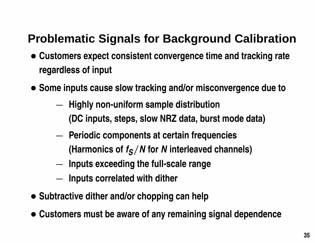
Problematic Signals for Background Calibration• Customers expect consistent convergence time and tracking rate
regardless of input
• Some inputs cause slow tracking and/or misconvergence due to
− Highly non-uniform sample distribution
(DC inputs, steps, slow NRZ data, burst mode data)
− Periodic components at certain frequencies
(Harmonics of fS/N for N interleaved channels)
− Inputs exceeding the full-scale range
− Inputs correlated with dither
• Subtractive dither and/or chopping can help
• Customers must be aware of any remaining signal dependence
35
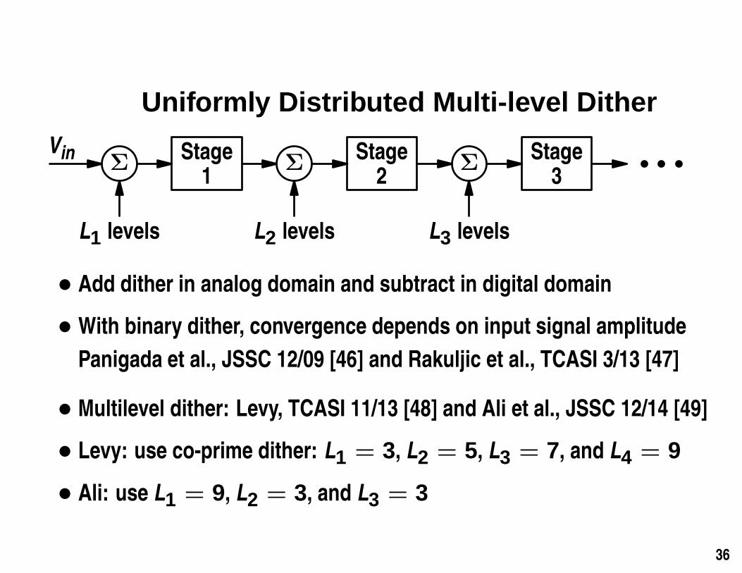
Uniformly Distributed Multi-level Dither
Vin Σ Stage1
Σ Stage2
Σ Stage3
L1 levels L2 levels L3 levels
• Add dither in analog domain and subtract in digital domain
• With binary dither, convergence depends on input signal amplitude
Panigada et al., JSSC 12/09 [46] and Rakuljic et al., TCASI 3/13 [47]
• Multilevel dither: Levy, TCASI 11/13 [48] and Ali et al., JSSC 12/14 [49]
• Levy: use co-prime dither: L1 = 3, L2 = 5, L3 = 7, and L4 = 9
• Ali: use L1 = 9, L2 = 3, and L3 = 3
36
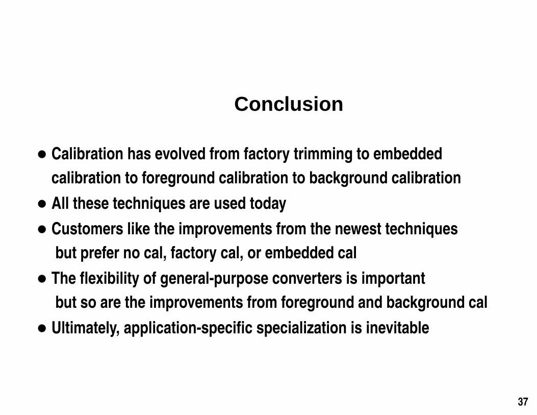
Conclusion
• Calibration has evolved from factory trimming to embedded
calibration to foreground calibration to background calibration
• All these techniques are used today
• Customers like the improvements from the newest techniques
but prefer no cal, factory cal, or embedded cal
• The flexibility of general-purpose converters is important
but so are the improvements from foreground and background cal
• Ultimately, application-specific specialization is inevitable
37
References
[1] P. Holloway and M. Norton, “A High-Yield, Second Generation 10-Bit Monolithic DAC,” IEEE InternationalSolid-State Circuits Conference, pp. 106–107, Feb. 1976.
[2] G. McGlinchey, “A Monolithic 12b 3µs ADC,” IEEE International Solid-State Circuits Conference, pp.80–81, Feb. 1982.
[3] M. de Wit, K.-S. Tan, and R. K. Hester, “A Low-Power 12-b Analog-to-Digital Converter with On-ChipPrecision Trimming,” IEEE J. of Solid-State Circuits, vol. 28, No. 4, pp. 455–461, Apr. 1993.
[4] H.-S. Lee, D. A. Hodges, and P. R. Gray, “A Self-Calibrating 15 Bit CMOS A/D Converter,” IEEE J. ofSolid-State Circuits, vol. SC-19, No. 6, pp. 813–819, Dec. 1984.
[5] D. W. J. Groeneveld, H. J. Schouwenaars, H. A. H. Termeer, and C. A. A. Bastiaansen, “A Self-CalibrationTechnique for Monolithic High-Resolution D/A Converters,” IEEE J. of Solid-State Circuits, vol. 24, No. 6,pp. 1517–1522, Dec. 1989.
[6] K.-S. Tan, S. Kiriaki, M. de Wit, J. W. Fattaruso, C.-Y. Tsay, W. E. Matthews, and R. K. Hester, “ErrorCorrection Techniques for High-Performance Differential A/D Converters,” IEEE J. of Solid-State Circuits,vol. 25, No. 6, pp. 1318–1327, Dec. 1990.
[7] T. Cataltepe, A. R. Kramer, L. E. Larson, G. C. Temes, and R. H. Walden, “Digitally Corrected Multi-bit Σ∆
Data Converters,” IEEE International Symposium on Circuits and Systems, pp. 647–650, May 1989.
[8] R. J. van de Plassche, “Dynamic Element Matching for High-Accuracy Monolithic D/A Converters,” IEEEJ. of Solid-State Circuits, vol. SC-11, No. 6, pp. 795–800, Dec. 1976.
38
[9] L. R. Carley and J. Kenney, “A 16-bit 4’th Order Noise-Shaping D/A Converter,” IEEE Custom IntegratedCircuits Conference, pp. 21.7.1–21.7.4, May 1988.
[10] B. H. Leung and S. Sutarja, “Multibit Σ-∆ A/D Converter Incorporating A Novel Class of Dynamic ElementMatching Techniques,” IEEE T. on Circuits and Systems II, vol. 39, No. 1, pp. 35–51, Jan. 1992.
[11] R. T. Baird and T. S. Fiez, “Linearity Enhancement of Multibit∆Σ A/D and D/A Converters using DataWeighted Averaging,” IEEE T. on Circuits and Systems II, vol. 42, No. 12, pp. 753–762, Dec. 1995.
[12] P. W. Li, M. J. Chin, P. R. Gray, and R. Castello, “A Ratio-Independent Algorithmic Analog-to-DigitalConversion Technique,” IEEE J. of Solid-State Circuits, vol. SC-19, No. 6, pp. 828–836, Dec. 1984.
[13] C.-C. Shih and P. R. Gray, “Reference Refreshing Cyclic Analog-to-Digital and Digital-to-AnalogConverters,” IEEE J. of Solid-State Circuits, vol. SC-21, No. 4, pp. 544–554, Aug. 1986.
[14] K. Nagaraj, T. R. Viswanathan, K. Singhal, and J. Vlach, “Switched-Capacitor Circuits with ReducedSensitivity to Amplifier Gain,” IEEE T. on Circuits and Systems, vol. CAS-34, No. 5, pp. 571–574, May 1987.
[15] B.-S. Song, M. F. Tompsett, and K. R. Lakshmikumar, “A 12-bit 1-Msample/s Capacitor Error-AveragingPipelined A/D Converter,” IEEE J. of Solid-State Circuits, vol. 23, No. 6, pp. 1324–1333, Dec. 1988.
[16] Y.-M. Lin, B. Kim, and P. R. Gray, “A 13-b 2.5-MHz Self-Calibrated Pipelined A/D Converter in 3-µm CMOS,”IEEE J. of Solid-State Circuits, vol. 26, No. 4, pp. 628–636, Apr. 1991.
[17] A. N. Karanicolas, H.-S. Lee, and K. L. Bacrania, “A 15-b 1-Msample/s Digitally Self-Calibrated PipelineADC,” IEEE J. of Solid-State Circuits, vol. 28, No. 12, pp. 1207–1215, Dec. 1993.
[18] R. Jewett, K. Poulton, K.-C. Hsieh, and J. Doernberg, “A 12b 128MSample/s ADC with 0.05LSB DNL,” IEEEInternational Solid-State Circuits Conference, pp. 138–139, Feb. 1997.
39
[19] H. E. Hilton, “A 10-MHz Analog-to-Digital Converter with 110-dB Linearity,” Hewlett-Packard Journal, vol.44, No. 5, pp. 105–112, Oct. 1993.
[20] E. J. Siragusa and I. Galton, “Gain error correction technique for pipelined analogue-to-digitalconverters,” Electronics Letters, vol. 36, No. 7, pp. 617–618, Mar. 30, 2000.
[21] J. Li and U.-K. Moon, “Background Calibration Techniques for Multistage Pipelined ADCs With DigitalRedundancy,” IEEE T. on Circuits and Systems II, vol. 50, No. 9, pp. 531–538, Sep. 2003.
[22] H. S. Fetterman, D. G. Martin, and D. A. Rich, “CMOS Pipelined ADC Employing Dither to ImproveLinearity,” IEEE Custom Integrated Circuits Conference, pp. 109-112, May 1999.
[23] B. Murmann and B. E. Boser, “A 12-bit 75-MS/s Pipelined ADC Using Open-Loop Residue Amplification,”IEEE J. of Solid-State Circuits, vol. 38, No. 12, pp. 2040–2050, Dec. 2003.
[24] J. McNeill, M. C. W. Coln, and B. J. Larivee, “"Split ADC" Architecture for Deterministic DigitalBackground Calibration of a 16-bit 1-MS/s ADC,” IEEE J. of Solid-State Circuits, vol. 40, No. 12, pp.2437–2445, Dec. 2005.
[25] X. Wang, P. J. Hurst, and S. H. Lewis, “A 12-bit 20-MS/s Pipelined ADC with Nested Digital BackgroundCalibration,” IEEE Custom Integrated Circuits Conference, pp. 409-412, Sep. 2003.
[26] Y. Chiu, C. W. Tsang, B. Nikolic, and P. R. Gray, “Least Mean Square Adaptive Digital BackgroundCalibration of Pipelined Analog-to-Digital Converters,” IEEE T. on Circuits and Systems I, vol. 51, No. 1,pp. 38–46, Jan. 2004.
[27] H. Wang, X. Wang, P. J. Hurst, and S. H. Lewis, “Nested Digital Background Calibration of a 12-bitPipelined ADC Without an Input SHA,” IEEE J. of Solid-State Circuits, vol. 44, No. 10, pp. 2780–2789, Oct.2009.
40
[28] I. Galton, “Digital Cancellation of D/A Converter Noise in Pipelined A/D Converters,” IEEE T. on Circuitsand Systems II, vol. 47, No. 3, pp. 185–196, Mar. 2000.
[29] W. C. Black, Jr. and D. A. Hodges, “Time Interleaved Converter Arrays,” IEEE J. of Solid-State Circuits,vol. SC-15, No. 6, pp. 1022–1029, Dec. 1980.
[30] H. van der Ploeg, G. Hoogzaad, H. A. H. Termeer, M. Vertregt, and R. L. J. Roovers, ”A 2.5-V 12-b54-Msample/s 0.25-µm CMOS ADC in 1-mm2 With Mixed-Signal Chopping and Calibration,” IEEE J. ofSolid-State Circuits, vol. 36, No. 12, pp. 1859–1867, Dec. 2001.
[31] S. M. Jamal, D. Fu, N. C.-J. Chang, P. J. Hurst, and S. H. Lewis, “A 10-b 120-Msample/s Time-InterleavedAnalog-to-Digital Converter With Digital Background Calibration,” IEEE J. of Solid-State Circuits, vol. 37,No. 12, pp. 1618–1627, Dec. 2002.
[32] E. Janssen, K. Doris, A. Zanikopoulos, A. Murroni, G. van der Weide, Y. Lin, L. Alvado, F. Darthenay, Y.Fregeais, “A 11b 3.6GS/s Time-Interleaved SAR ADC in 65nm CMOS,” IEEE International Solid-StateCircuits Conference, pp. 464–465, Feb. 2013.
[33] B. Setterberg, K. Poulton, S. Ray, D. J. Huber, V. Abramzon, G. Steinbach, J. P. Keane, B. Wuppermann, M.Clayson, M. Martin, R. Pasha, E. Peeters, A. Jacobs, F. Demarsin, A. Al-Adnani, P. Brandt, “A 14b 2.5GS/s8-Way-Interleaved Pipelined ADC with Background Calibration and Digital Dynamic Linearity Correction,”IEEE International Solid-State Circuits Conference, pp. 466–467, Feb. 2013.
[34] D. Fu, K. C. Dyer, P. J. Hurst, and S. H. Lewis, “A Digital Background Calibration Technique forTime-Interleaved Analog-to-Digital Converters,” IEEE J. of Solid-State Circuits, vol. 33, No. 12, pp.1904–1911, Dec. 1998.
[35] M. El-Chammas and B. Murmann, “A 12-GS/s 81-mW 5-bit Time-Interleaved Flash ADC With BackgroundTiming Skew Calibration,” IEEE J. of Solid-State Circuits, vol. 46, No. 4, pp. 838–847, Apr. 2011.
41
[36] D. Stepanovic and B. Nikolic, “A 2.8 GS/s 44.6mW Time-Interleaved ADC Achieving 50.9 dB SNDR and 3dB Effective Resolution Bandwidth of 1.5 GHz in 65 nm CMOS,” IEEE J. of Solid-State Circuits, vol. 48, No.4, pp. 971–982, Apr. 2013.
[37] B.-R.-S. Sung, C.-K. Lee, W. Kim, J.-I. Kim, H.-K. Hong, G.-G. Oh, C.-H. Lee, M. Choi, H.-J. Park, and S.-T.Ryu, “A 6 bit 2 GS/s Flash-Assisted Time-Interleaved (FATI) SAR ADC with Background OffsetCalibration,” IEEE Asian Solid-State Circuits Conference, pp. 281–284, Nov. 2013.
[38] S. Lee, A. P. Chandrakasan, H.-S. Lee, “A 1GS/s 10b 18.9mW Time-Interleaved SAR ADC with BackgroundTiming-Skew Calibration,” IEEE International Solid-State Circuits Conference, pp. 384–385, Feb. 2014.
[39] B.-R.-S. Sung, D.-S. Jo, I.-H. Jang, D.-S. Lee, Y.-S. You, Y.-H. Lee, H.-J. Park, and S.-T. Ryu, “A21fJ/conv-step 9 ENOB 1.6GS/s 2x Time-Interleaved FATI SAR ADC with Background Offset andTiming-Skew Calibration in 45nm CMOS,” IEEE International Solid-State Circuits Conference, pp.464–465, Feb. 2015.
[40] K. Poulton, J. J. Corcoran, and T. Hornak, “A 1-GHz 6-bit ADC System,” IEEE J. of Solid-State Circuits,vol. SC-22, No. 6, pp. 962–970, Dec. 1987.
[41] K. C. Dyer, D. Fu, P. J. Hurst, and S. H. Lewis, “An Analog Background Calibration Technique forTime-Interleaved Analog-to-Digital Converters,” IEEE J. of Solid-State Circuits, vol. 33, No. 12, pp.1912–1919, Dec. 1998.
[42] K. Poulton, R. Neff, A. Muto, W. Liu, A. Burstein, and M. Heshami, “A 4 GSample/s 8b ADC in 0.35µmCMOS,” IEEE International Solid-State Circuits Conference, pp. 166–167, Feb. 2002.
[43] K. Doris, E. Janssen, C. Nani, A. Zanikopoulos, G. van der Weide, “A 480 mW 2.6 GS/s 10bTime-Interleaved ADC With 48.5 dB SNDR up to Nyquist in 65 nm CMOS,” IEEE J. of Solid-State Circuits,vol. 46, No. 12, pp. 2821–2833, Dec. 2011.
42
[44] N. Le Dortz, J.-P. Blanc, T. Simon, S. Verhaeren, E. Rouat, P. Urard, S. Le Tual, D. Goguet, C.Lelandais-Perrault, P. Benabes, “A 1.62GS/s Time-Interleaved SAR ADC with Digital BackgroundMismatch Calibration Achieving Interleaving Spurs Below 70 dBFS,” IEEE International Solid-StateCircuits Conference, pp. 386–387, Feb. 2014.
[45] L. Kull, T. Toifl, M. Schmatz, P. A. Francese, C. Menolfi, M. Braendil, M. Kossel, T. Morf, T. M. Andersen, Y.Leblebici, “A 90GS/s 8b 667mW 64x Interleaved SAR ADC in 32nm Digital SOI CMOS,” IEEE InternationalSolid-State Circuits Conference, pp. 378–379, Feb. 2014.
[46] A. Panigada and I. Galton, “A 130 mW 100 MS/s Pipelined ADC With 69 dB SNDR Enabled by DigitalHarmonic Distortion Correction,” IEEE J. of Solid-State Circuits, vol. 44, No. 12, pp. 3314–3328, Dec. 2009.
[47] N. Rakuljic and I. Galton, “Suppression of Quantization-Induced Convergence Error in Pipelined ADCsWith Harmonic Distortion Correction,” IEEE T. on Circuits and Systems I, vol. 60, No. 3, pp. 593–602, Mar.2013.
[48] B. C. Levy, “A Study of Subtractive Digital Dither in Single-Stage and Multi-Stage Quantizers,” IEEE T. onCircuits and Systems I, vol. 60, No. 11, pp. 2888–2901, Nov. 2013.
[49] A. M. A. Ali, H. Dinc, P. Bhoraskar, C. Dillon, S. Puckett, B. Gray, C. Speir, J. Lanford, J. Brunsilius, P. R.Derounian, B. Jeffries, U. Mehta, M. McShea, and R. Stop, “A 14 Bit 1 GS/s RF Sampling Pipelined ADCWith Background Calibration,” IEEE J. of Solid-State Circuits, vol. 49, No. 12, pp. 2857–2867, Dec. 2014.
43