Embed Size (px)
Citation preview
Introduction
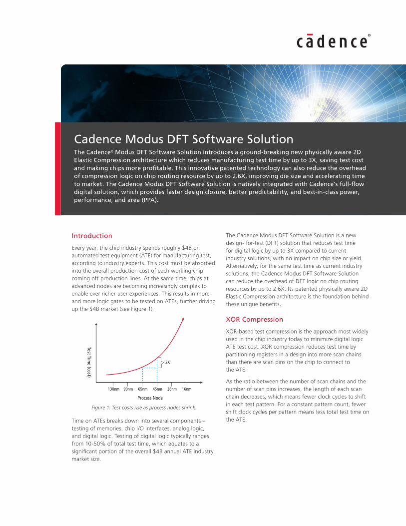
Every year, the chip industry spends roughly $4B on automated test equipment (ATE) for manufacturing test, according to industry experts. This cost must be absorbed into the overall production cost of each working chip coming off production lines. At the same time, chips at advanced nodes are becoming increasingly complex to enable ever richer user experiences. This results in more and more logic gates to be tested on ATEs, further driving up the $4B market (see Figure 1).
130nm 90nm 65nm
Process Node
Test Time (cost)
45nm
2X
28nm 16nm
Time on ATEs breaks down into several components – testing of memories, chip I/O interfaces, analog logic, and digital logic. Testing of digital logic typically ranges from 10-50% of total test time, which equates to a significant portion of the overall $4B annual ATE industry market size.
The Cadence Modus DFT Software Solution is a new design- for-test (DFT) solution that reduces test time for digital logic by up to 3X compared to current industry solutions, with no impact on chip size or yield. Alternatively, for the same test time as current industry solutions, the Cadence Modus DFT Software Solution can reduce the overhead of DFT logic on chip routing resources by up to 2.6X. Its patented physically aware 2D Elastic Compression architecture is the foundation behind these unique benefits.
XOR Compression
XOR-based test compression is the approach most widely used in the chip industry today to minimize digital logic ATE test cost. XOR compression reduces test time by partitioning registers in a design into more scan chains than there are scan pins on the chip to connect to the ATE.
As the ratio between the number of scan chains and the number of scan pins increases, the length of each scan chain decreases, which means fewer clock cycles to shift in each test pattern. For a constant pattern count, fewer shift clock cycles per pattern means less total test time on the ATE.
Figure 1: Test costs rise as process nodes shrink.
Cadence Modus DFT Software SolutionThe Cadence® Modus DFT Software Solution introduces a ground-breaking new physically aware 2D Elastic Compression architecture which reduces manufacturing test time by up to 3X, saving test cost and making chips more profitable. This innovative patented technology can also reduce the overhead of compression logic on chip routing resource by up to 2.6X, improving die size and accelerating time to market. The Cadence Modus DFT Software Solution is natively integrated with Cadence’s full-flow digital solution, which provides faster design closure, better predictability, and best-in-class power, performance, and area (PPA).
www.cadence.com 2
Compression Ratio Impact on Coverage and Test Time
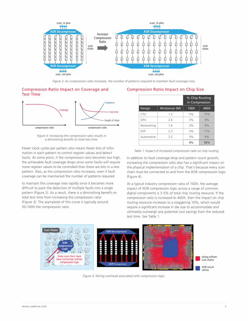
Fewer clock cycles per pattern also means fewer bits of infor- mation in each pattern to control register values and detect faults. At some point, if the compression ratio becomes too high, the achievable fault coverage drops since some faults will require more register values to be controlled than there are bits in a test pattern. Also, as the compression ratio increases, even if fault coverage can be maintained the number of patterns required
to maintain this coverage rises rapidly since it becomes more difficult to pack the detection of multiple faults into a single pattern (Figure 2). As a result, there is a diminishing benefit on total test time from increasing the compression ratio (Figure 3). The asymptote of this curve is typically around 50-100X the compression ratio.
Compression Ratio Impact on Chip Size
% Chip Routing in Compression
Design #Instances (M) 100X 400X
CPU 1.3 5% 15%
GPU 2.6 3% 8%
Networking 1.6 3% 9%
DSP 2.3 5% 11%
Automotive 2.5 3% 6%
4% 10%
In addition to fault coverage drop and pattern count growth, increasing the compression ratio also has a significant impact on the physical implementation of a chip. That’s because every scan chain must be connected to and from the XOR compression logic (Figure 4).
At a typical industry compression ratio of 100X, the average impact of XOR compression logic across a range of common digital components is 3-5% of total chip routing resource. If the compression ratio is increased to 400X, then the impact on chip routing resource increases to a staggering 10%, which would require a significant increase in die size to accommodate and ultimately outweigh any potential cost savings from the reduced test time. See Table 1.
scanchain
scanchain
IncreaseCompression
Ratio
scan_out pins
XOR Decompressor
XOR Decompressor
scan_in pinsscan_in pins
scan_out pins
XOR Decompressor
XOR DecompressorXOR Decompressor
Figure 2: As compression ratio increases, the number of patterns required to maintain fault coverage rises.
compression ratio compression ratio
coverage
# patterns
test time
length of chain
XORCompression
Logic
Scan Chains
Every scan chain must have connection to/from
compression logic
wiring to/fromscan chains
XOR circuitwiring
Figure 3: Increasing the compression ratio results in a diminishing benefit on total test time.
Figure 4: Wiring overhead associated with compression logic.
Table 1: Impact of increased compression ratio on chip routing.
www.cadence.com 3
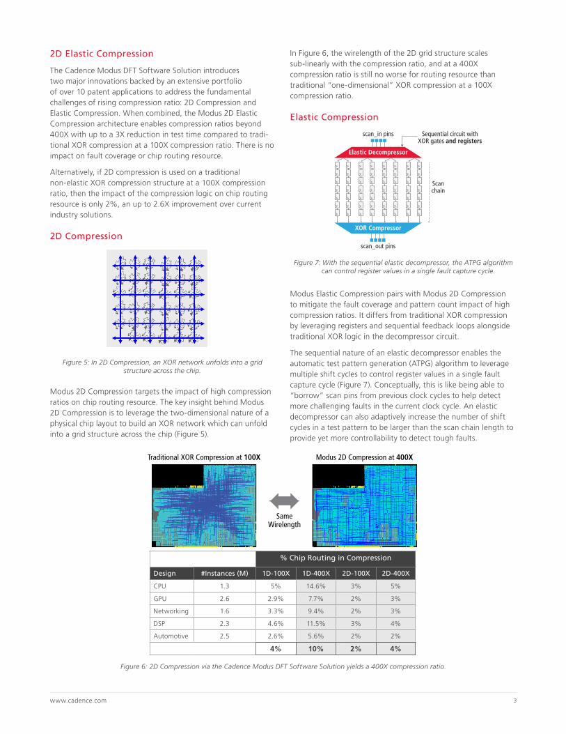
2D Elastic Compression
The Cadence Modus DFT Software Solution introduces two major innovations backed by an extensive portfolio of over 10 patent applications to address the fundamental challenges of rising compression ratio: 2D Compression and Elastic Compression. When combined, the Modus 2D Elastic Compression architecture enables compression ratios beyond 400X with up to a 3X reduction in test time compared to tradi-tional XOR compression at a 100X compression ratio. There is no impact on fault coverage or chip routing resource.
Alternatively, if 2D compression is used on a traditional non-elastic XOR compression structure at a 100X compression ratio, then the impact of the compression logic on chip routing resource is only 2%, an up to 2.6X improvement over current industry solutions.
2D Compression
Modus 2D Compression targets the impact of high compression ratios on chip routing resource. The key insight behind Modus 2D Compression is to leverage the two-dimensional nature of a physical chip layout to build an XOR network which can unfold into a grid structure across the chip (Figure 5).
In Figure 6, the wirelength of the 2D grid structure scales sub-linearly with the compression ratio, and at a 400X compression ratio is still no worse for routing resource than traditional “one-dimensional” XOR compression at a 100X compression ratio.
Elastic Compression
Modus Elastic Compression pairs with Modus 2D Compression to mitigate the fault coverage and pattern count impact of high compression ratios. It differs from traditional XOR compression by leveraging registers and sequential feedback loops alongside traditional XOR logic in the decompressor circuit.
The sequential nature of an elastic decompressor enables the automatic test pattern generation (ATPG) algorithm to leverage multiple shift cycles to control register values in a single fault capture cycle (Figure 7). Conceptually, this is like being able to “borrow” scan pins from previous clock cycles to help detect more challenging faults in the current clock cycle. An elastic decompressor can also adaptively increase the number of shift cycles in a test pattern to be larger than the scan chain length to provide yet more controllability to detect tough faults.
Traditional XOR Compression at 100X
SameWirelength
Modus 2D Compression at 400X
Figure 6: 2D Compression via the Cadence Modus DFT Software Solution yields a 400X compression ratio.
Figure 5: In 2D Compression, an XOR network unfolds into a grid structure across the chip.
Scanchain
scan_out pins
Elastic Decompressor
XOR Compressor
scan_in pins Sequential circuit withXOR gates and registers
Figure 7: With the sequential elastic decompressor, the ATPG algorithm can control register values in a single fault capture cycle.
% Chip Routing in Compression
Design #Instances (M) 1D-100X 1D-400X 2D-100X 2D-400X
CPU 1.3 5% 14.6% 3% 5%
GPU 2.6 2.9% 7.7% 2% 3%
Networking 1.6 3.3% 9.4% 2% 3%
DSP 2.3 4.6% 11.5% 3% 4%
Automotive 2.5 2.6% 5.6% 2% 2%
4% 10% 2% 4%
Cadence software, hardware and semiconductor IP enable electronic systems and semiconductor companies to create the innovative end products that are transforming the way people live, work, and play. The company’s System Design Enablement strategy helps customers develop differentiated products— from chips to boards to systems. www.cadence.com
© 2017 Cadence Design Systems, Inc. All rights reserved worldwide. Cadence, the Cadence logo, and the other Cadence marks found at www.cadence.com/go/trademarks are trademarks or registered trademarks of Cadence Design Systems, Inc. All other trademarks are the property of their respective owners. 9703 10/17 SA/LL/PDF
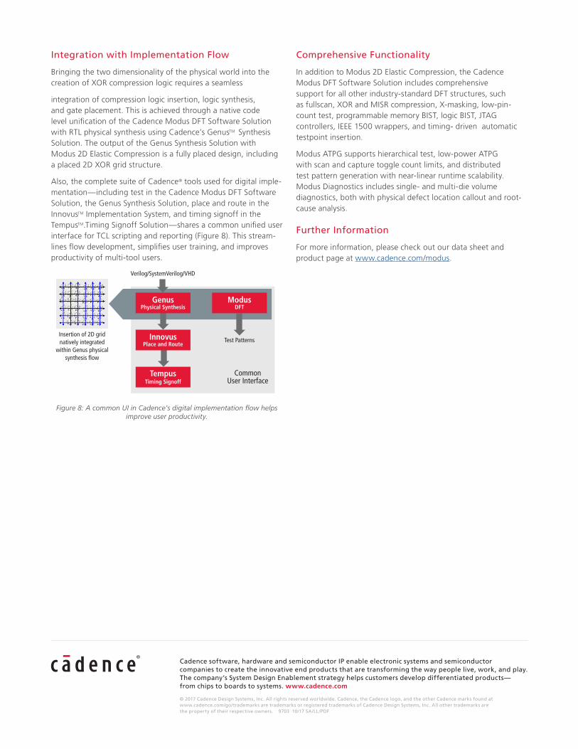
Integration with Implementation Flow
Bringing the two dimensionality of the physical world into the creation of XOR compression logic requires a seamless
integration of compression logic insertion, logic synthesis, and gate placement. This is achieved through a native code level unification of the Cadence Modus DFT Software Solution with RTL physical synthesis using Cadence’s GenusTM Synthesis Solution. The output of the Genus Synthesis Solution with Modus 2D Elastic Compression is a fully placed design, including a placed 2D XOR grid structure.
Also, the complete suite of Cadence® tools used for digital imple-mentation—including test in the Cadence Modus DFT Software Solution, the Genus Synthesis Solution, place and route in the InnovusTM Implementation System, and timing signoff in the TempusTM.Timing Signoff Solution—shares a common unified user interface for TCL scripting and reporting (Figure 8). This stream-lines flow development, simplifies user training, and improves productivity of multi-tool users.
Comprehensive Functionality
In addition to Modus 2D Elastic Compression, the Cadence Modus DFT Software Solution includes comprehensive support for all other industry-standard DFT structures, such as fullscan, XOR and MISR compression, X-masking, low-pin-count test, programmable memory BIST, logic BIST, JTAG controllers, IEEE 1500 wrappers, and timing- driven automatic testpoint insertion.
Modus ATPG supports hierarchical test, low-power ATPG with scan and capture toggle count limits, and distributed test pattern generation with near-linear runtime scalability. Modus Diagnostics includes single- and multi-die volume diagnostics, both with physical defect location callout and root-cause analysis.
Further Information
For more information, please check out our data sheet and product page at www.cadence.com/modus.
GenusPhysical Synthesis
ModusDFT
Test Patterns
Verilog/SystemVerilog/VHD
CommonUser Interface
InnovusPlace and Route
TempusTiming Signoff
Insertion of 2D grid natively integrated
within Genus physical synthesis flow
Figure 8: A common UI in Cadence’s digital implementation flow helps improve user productivity.