Embed Size (px)
Citation preview

Electrical & Computer Engineering Technology
EET 4158C – Linear integrated circuits & systems
Laboratory Experiments
by
Masood Ejaz

EET 4158C – Linear Integrated Circuits & Systems Electrical & Computer Engineering Technology
2 Valencia College
EXPERIMENT # 1
Inverting and Non-Inverting Amplifiers
Prelab: Calculate closed-loop gain, output voltage, and input resistance for both amplifiers
theoretically. Design both amplifiers in PSpice and perform all of the procedural steps. Op-amp
is present in the eval library.
Note: Save all of your waveforms from the oscilloscope for your lab report. Saved waveform
should show all of the relevant information.
Procedure:
Inverting Amplifier
1. Design the inverting amplifier as shown in figure 1. Op-amp is 741, Rf = 10K, and Rin =
1KUse ±15V to bias the Op-amp and choose vin = 1V (peak), 1KHz sinusoidal signal.
Make sure to connect both input and output terminals of the op-amp to the two channels of
the oscilloscope. Observe the output and calculate the practical value of gain. Also, confirm
that inverting relationship does exist between input and output.
Figure 1: Inverting Amplifier
2. Measure the input resistance of the circuit by inserting a variable resistor between vin and Rin
and changing its value until the output voltage becomes half of what you measured in step 1.
Measure the value of the variable resistor. This is your approximate input resistance of the
circuit.
rin = ______________________________
3. Remove the resistance that you inserted in the last step and go back to the original circuit.
Increase the input voltage and observe its value when the output reaches to the saturation
limits. This is the maximum input voltage for linear operation.
EET 4158C – Linear Integrated Circuits & Systems Electrical & Computer Engineering Technology
3 Valencia College
vin = ______________________; vout = ______________________
Non-Inverting Amplifier
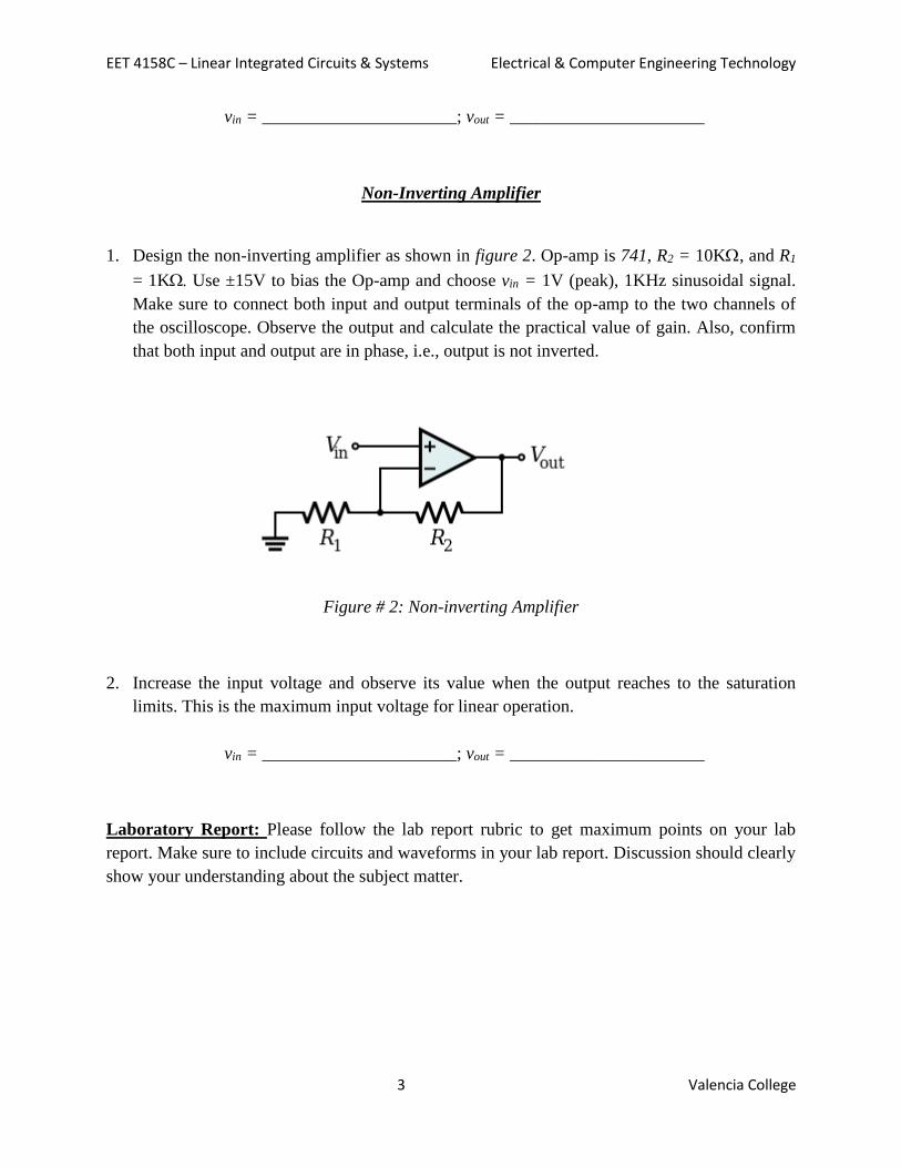
1. Design the non-inverting amplifier as shown in figure 2. Op-amp is 741, R2 = 10K, and R1
= 1KUse ±15V to bias the Op-amp and choose vin = 1V (peak), 1KHz sinusoidal signal.
Make sure to connect both input and output terminals of the op-amp to the two channels of
the oscilloscope. Observe the output and calculate the practical value of gain. Also, confirm
that both input and output are in phase, i.e., output is not inverted.
Figure # 2: Non-inverting Amplifier
2. Increase the input voltage and observe its value when the output reaches to the saturation
limits. This is the maximum input voltage for linear operation.
vin = ______________________; vout = ______________________
Laboratory Report: Please follow the lab report rubric to get maximum points on your lab
report. Make sure to include circuits and waveforms in your lab report. Discussion should clearly
show your understanding about the subject matter.

EET 4158C – Linear Integrated Circuits & Systems Electrical & Computer Engineering Technology
4 Valencia College
EXPERIMENT # 2
Linear Combination Circuits: Summing & Differential Amplifiers
Prelab:Write down the expressions for the output voltages for both the circuits.
Summing Amplifier: ____________________________________________________
Differential Amplifier: __________________________________________________
Design both the amplifiers in PSpice and perform all of the procedural steps.Op-amp is present
in the eval library.
Note: (i) Save all of your waveforms from the oscilloscope for your lab report. Saved waveform
should show all of the relevant information. Make sure to change the format of the waveforms
from wav to bmp before you save them.(ii) Make sure to set the reference (GND) for both the
channels of the oscilloscope right in the center. Once you set the proper reference then change
both the channels to ‘DC’ to observe the properly shifted waveforms.
Procedure:
Summing Amplifier
4. Design the summing amplifier as shown in figure 1. Op-amp is 741. Use ±15V to bias the
Op-amp.
Figure 1: Op-Amp Two Input Summing Amplifier
5. Apply two convenient DC voltages to v1and v2 such that the magnitude of the combined sum
of both is less than or equal to 12V. Measure the output voltage and compare it with the
theoretical value.
OPAMP
+
-
OUT
R1
10k
R2
10k
R3
10k
0
v2
v1
vout

EET 4158C – Linear Integrated Circuits & Systems Electrical & Computer Engineering Technology
5 Valencia College
vout (expected) = _________________________; vout (measured) = __________________;
6. Apply a negative DC voltage to one of the inputs and a 1KHz sinusoid to the other input.
Make sure that the combined sum of the magnitude of DC voltage and peak value of sinusoid
is less or equal to 12V. Observe the output voltage on the oscilloscope and compare the
expected maximum and minimum values of the output voltage with their expected values.
vout (expected) = _________________________; vout (measured) = __________________;
Differential Amplifier
7. Design the differential amplifier as shown in figure 2. Op-amp is 741.Use ±15V to bias the
Op-amp.
Figure 2: Closed-Loop Differential Amplifier
8. Apply two convenient DC voltages to v1and v2 such that the magnitude of the theoretical
output will be less than or equal to 12V. Measure the output voltage and compare it with the
theoretical value.
vout (expected) = _________________________; vout (measured) = __________________;
9. Apply a negative DC voltage to one of the inputs and a 1KHz sinusoid to the other input.
Make sure that the magnitude of the theoretical output values should be less or equal to 12V.
Observe the output voltage on the oscilloscope and compare the expected maximum and
minimum values of the output voltage with their expected values.
OPAMP
+
-
OUT
R1
1k
R2
1k
R3
2k
R4
2k
0
v2
v1
vout

EET 4158C – Linear Integrated Circuits & Systems Electrical & Computer Engineering Technology
6 Valencia College
vout (expected) = _________________________; vout (measured) = __________________;
Laboratory Report: Please follow the lab report rubric to get maximum points on your lab
report. Make sure to include circuits and waveforms in your lab report. Discussion should clearly
show your understanding about the subject matter.

EET 4158C – Linear Integrated Circuits & Systems Electrical & Computer Engineering Technology
7 Valencia College
EXPERIMENT # 3
OPERATIONAL AMPLIFIER CLOSED-LOOP BANDWIDTH
Prelab: Write down the expression for the closed-loop voltage gain (as a function of frequency)
for the circuit and calculate the value of closed-loop bandwidth BCL for the circuit. Fill out other
theoretical information as required under the Procedure.
Closed-Loop Voltage Gain and BCL: ________________________________________________
Design the amplifier in PSpice and perform all of the procedural steps. Op-amp is present in the
eval library.
Note: Save all of your waveforms from the oscilloscope for your lab report. Saved waveform
should show all of the relevant information. Make sure to change the format of the waveforms
from wav to bmp before you save them.
Procedure:
1. Connect the inverting amplifier as shown in figure 1 with Rin = 1K and Rf= 10KUse
±15V for biasing voltages. Use vin to be a sinusoid with peak value to be 50mV. Choose a
very small frequency (close to DC) and measure the output voltage. Compare your measured
and expected values.
vout (expected) = _____________________; vout (measured) = _____________________
2. Increase the frequency to the calculated 3-db frequency. Once again, compare the expected
and observed outputs. If you see any discrepancy between the expected and measured
outputs, explain the reason.
vout (expected) = _____________________; vout (measured) = _____________________
Figure 1: Inverting Amplifier

EET 4158C – Linear Integrated Circuits & Systems Electrical & Computer Engineering Technology
8 Valencia College
3. Observe output voltage for a number of different frequency values to yield a graph between
vout vs. f for your lab report (Use MATLAB to create graph; instead of plot, use semilogx to
get a better picture of the response). Compare this plot with the PSpice simulation of the
circuit (AC sweep).
Laboratory Report: Please follow the lab report rubric to get maximum points on your lab
report. Make sure to include circuits and waveforms in your lab report. Discussion should clearly
show your understanding about the subject matter.

EET 4158C – Linear Integrated Circuits & Systems Electrical & Computer Engineering Technology
9 Valencia College
EXPERIMENT # 4
AC INTEGRATOR & LOW-FREQUENCY DIFFERENTIATOR
Prelab: Write down the frequency-domain expression for the output voltage for both the circuits
and calculate the value of the 3-dB frequency.
Vout(j) and fb for the AC integrator: _______________________________________________
Vout(j) and fb for the low-frequency differentiator:___________________________________
Write down the time-domain expression for the output voltage for both the circuits assuming that
the operating frequency is quite larger than the break frequency for the integrator circuit and
quire smaller for the differentiator circuit.
vo(t) for the AC integrator: ___________________________________________________
vo(t) for the low-frequency differentiator: ____________________________________________
Design the circuits in PSpice and perform all of the procedural steps. Make sure to run the
circuits until steady-state is reached. Op-amp is present in the eval library.
Note: Save all of your waveforms from the oscilloscope for your lab report. Saved waveform
should show all the relevant information. Make sure to change the format of the waveforms from
wav to bmp before you save them. Also, keep your oscilloscope channels at DC coupling once
you set the reference coupling (GND) to be in the center of the oscilloscope screen for both the
channels.
Procedure:
AC Integrator
4. Connect the AC Integrator as shown in figure 1 with Rin = 1K, Rf= 10Kand C =
1FUse ±15V for biasing voltages.
C1
1u
Rf
10k
Rin
1k
U1
OPAMP
+
-
OUT
0
vinvout

EET 4158C – Linear Integrated Circuits & Systems Electrical & Computer Engineering Technology
10 Valencia College
Figure 1: AC Integrator
5. Use vin to be a square wave with peak value to be 4V (4V to -4V) and frequency to be 1 KHz.
Make sure that there is no DC offset for the square wave. Compare the output waveform
shape and maximum and minimum observed values against the expected ones. Make sure to
support your expected results with proper calculations.
vout shape and extreme values (expected) : ______________________________________
vout shape and extreme values (observed) : ______________________________________
6. Introduce a 1V DC offset to the input square wave. Hence, now input is a square wave with
maximum value of 5V and minimum value of -3V. Keep frequency to be 1KHz. Compare
the output waveform shape and maximum and minimum observed values against the
expected ones. Make sure to support your expected results with proper calculations.
vout shape and extreme values (expected) : ______________________________________
vout shape and extreme values (observed) : ______________________________________
7. Change vin to a triangular wave with peak value to be 4V (4V to -4V) and frequency to be 1
KHz. Make sure that there is no DC offset for the square wave. Compare the output
waveform shape and maximum and minimum observed values against the expected ones.
Make sure to support your expected results with proper calculations.
vout shape and extreme values (expected) : ______________________________________
vout shape and extreme values (observed) : ______________________________________
8. Introduce a 1V DC offset to the input triangular wave. Hence, now input is a triangular wave
with maximum value of 5V and minimum value of -3V. Keep frequency to be 1KHz.
Compare the output waveform shape and maximum and minimum observed values against
the expected ones. Make sure to support your expected results with proper calculations.
vout shape and extreme values (expected) : ______________________________________
vout shape and extreme values (observed) : ______________________________________
EET 4158C – Linear Integrated Circuits & Systems Electrical & Computer Engineering Technology
11 Valencia College
Low-Frequency Differentiator
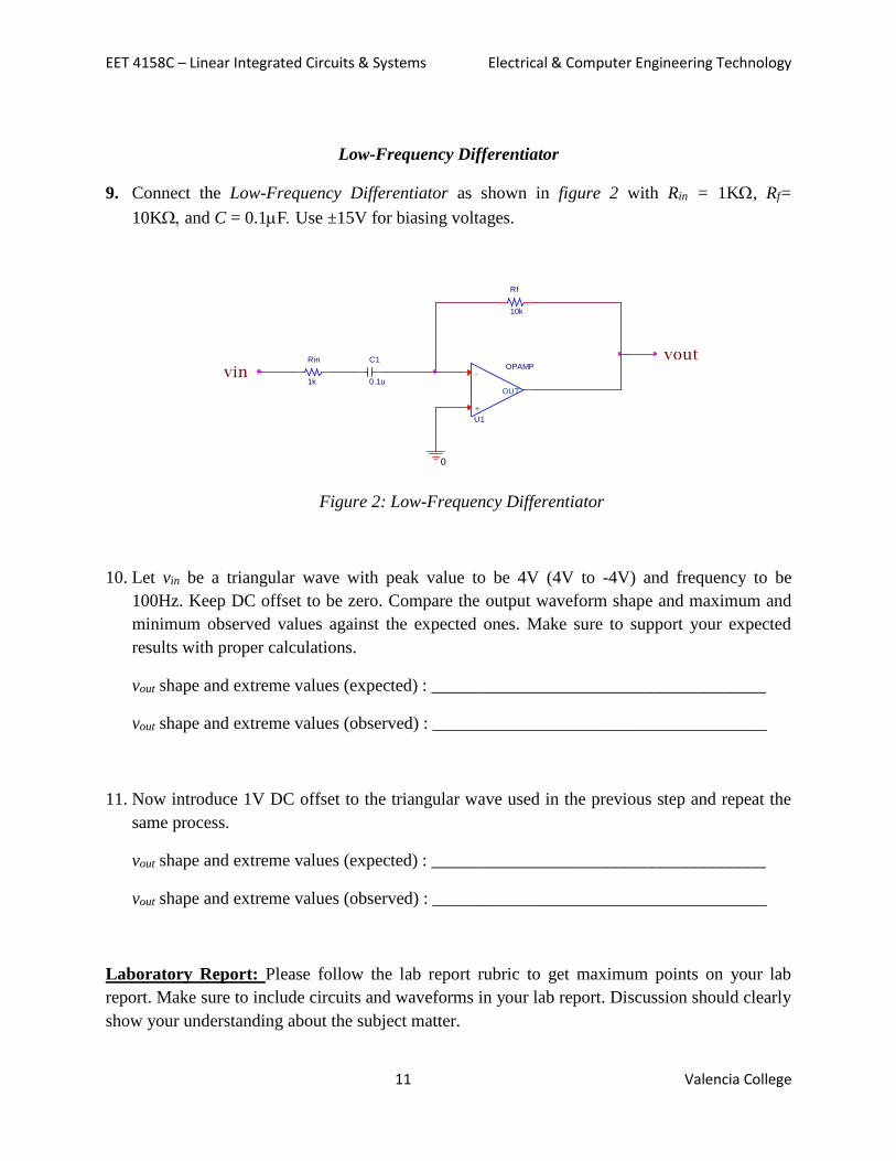
9. Connect the Low-Frequency Differentiator as shown in figure 2 with Rin = 1K, Rf=
10Kand C = 0.1FUse ±15V for biasing voltages.
Figure 2: Low-Frequency Differentiator
10. Let vin be a triangular wave with peak value to be 4V (4V to -4V) and frequency to be
100Hz. Keep DC offset to be zero. Compare the output waveform shape and maximum and
minimum observed values against the expected ones. Make sure to support your expected
results with proper calculations.
vout shape and extreme values (expected) : ______________________________________
vout shape and extreme values (observed) : ______________________________________
11. Now introduce 1V DC offset to the triangular wave used in the previous step and repeat the
same process.
vout shape and extreme values (expected) : ______________________________________
vout shape and extreme values (observed) : ______________________________________
Laboratory Report: Please follow the lab report rubric to get maximum points on your lab
report. Make sure to include circuits and waveforms in your lab report. Discussion should clearly
show your understanding about the subject matter.
Rf
10k
Rin
1k
U1
OPAMP
+
-
OUT
0
vinvoutC1
0.1u

EET 4158C – Linear Integrated Circuits & Systems Electrical & Computer Engineering Technology
12 Valencia College
EXPERIMENT # 5
555 Timer AstableMultivibrator
Prelab: For the 555 timer circuit shown in figure 1, calculate the values for RAand RB for
frequency of the output to be 1KHz with 60% duty cycle.
Equation to calculate RB = __________________________________________________
Value of RB = ____________________________________________________________
Equation to calculate RA = __________________________________________________
Value of RA = ____________________________________________________________
Design the circuits in PSpice and perform all of the procedural steps.Make sure to run the
circuits until steady-state is reached.555 timer is present in the eval library.
Note: Save all of your waveforms from the oscilloscope for your lab report. Saved waveform
should show all the relevant information. Make sure to change the format of the waveforms from
wav to bmp before you save them.
Procedure:
1. Design the circuit shown in figure 1 with the values that you calculated in the prelab. Choose
C = 10nF. Also, use a 10Kload at the output.
Figure 1: 555 Timer AstableMultivibrator

EET 4158C – Linear Integrated Circuits & Systems Electrical & Computer Engineering Technology
13 Valencia College
2. Connect the output to oscilloscope and measure the output frequency and duty cycle.
fout= __________________________; Duty Cycle = _______________________;
3. If your values for the frequency and duty cycle are quite different from the expected ones,
measure the exact values of your resistors and capacitor and calculate the output frequency
and duty cycle based on the calculated values. Compare the results against your observed
values.
RA(measured) = ___________; RB (measured) = ____________; C(measured) = _________
f (expected) = _______________; Duty Cycle (expected) = ____________________
Laboratory Report: Please follow the lab report rubric to get maximum points on your lab
report. Make sure to include circuits and waveforms in your lab report. Discussion should clearly
show your understanding about the subject matter.
EET 4158C – Linear Integrated Circuits & Systems Electrical & Computer Engineering Technology
14 Valencia College
EXPERIMENT # 6
Low-Pass Butterworth Unity-Gain Active Filter
Prelab: For the normalized unity-gain four-pole low-pass Butterworth filter, as shown in figure
1, calculate the values for the components to satisfy the following conditions. Normalized cut-off
frequency for the filteris 1 rad/sec.
fc = 5KHz; C1(final) = C3(final) = 10nF
Stage 1: C2(final) = ________; R1(final) = R2(final) = __________; Rbias1(final) = __________
Stage 2: C4(final) = ________; R3(final) = R4(final) = __________; Rbias2(final) = __________
Design the circuit in PSpice and perform all of the procedural steps.To get the frequency
response, use AC Sweep. Use Op-Amp 741 from eval library.
Note: Save all of your waveforms from the oscilloscope for your lab report. Saved waveform
should show all the relevant information. Make sure to change the format of the waveforms from
wav to bmp before you save them.
Procedure:
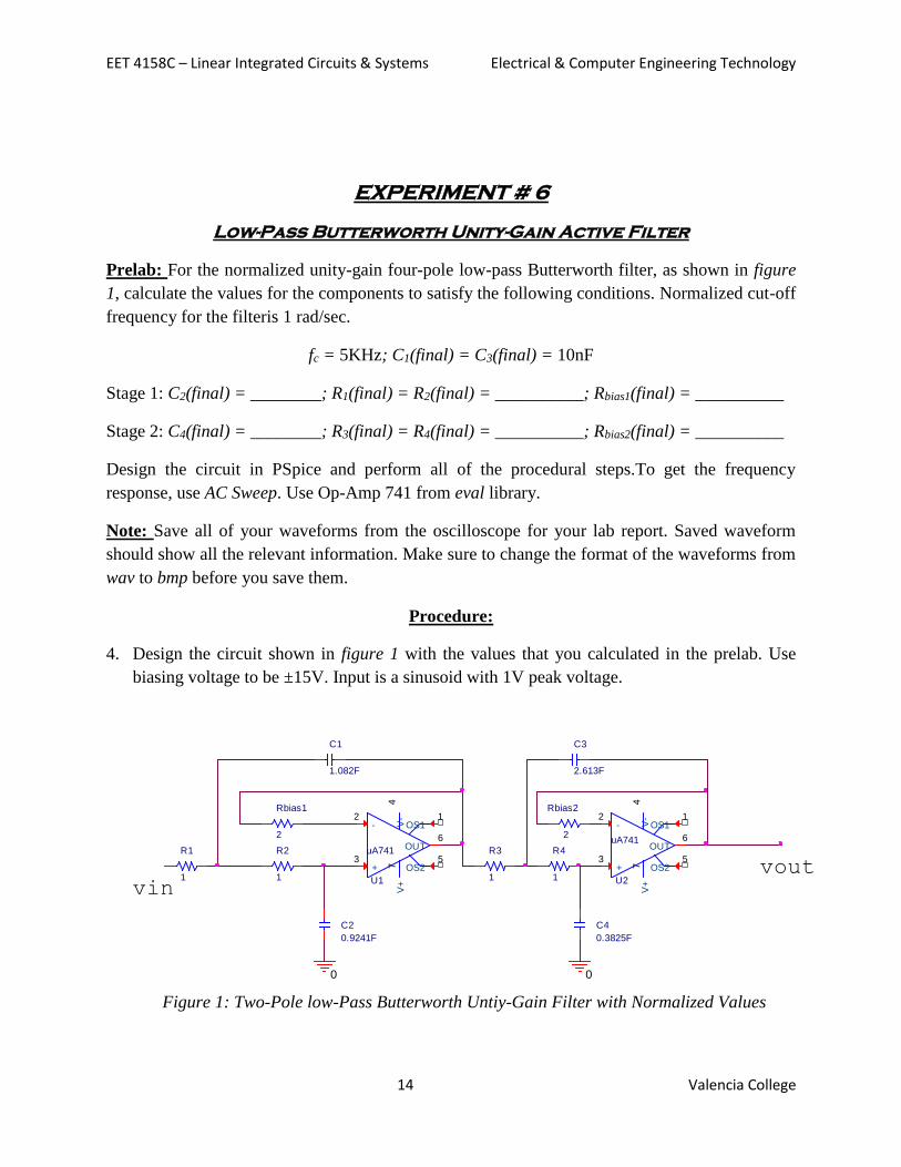
4. Design the circuit shown in figure 1 with the values that you calculated in the prelab. Use
biasing voltage to be ±15V. Input is a sinusoid with 1V peak voltage.
Figure 1: Two-Pole low-Pass Butterworth Untiy-Gain Filter with Normalized Values
U1
uA741
+3
-2
V+
7V
-4
OUT6
OS11
OS25
U2
uA741
+3
-2
V+
7V
-4
OUT6
OS11
OS25
C1
1.082F
C2
0.9241F
C3
2.613F
C4
0.3825F
R1
1
R2
1
R3
1
R4
1
Rbias1
2
Rbias2
2
0 0
voutvin

EET 4158C – Linear Integrated Circuits & Systems Electrical & Computer Engineering Technology
15 Valencia College
5. Connect the output to the oscilloscope and measure its peak value at the expected cut-off
frequency (5KHz). If expected cut-off is not correct, observe the practical cut-off frequency
by changing the input frequency until the output goes down to 0.7071V (peak).
voat fc (expected) = ________________________; fc (practical) = ________________
6. Observe several values for the output at different frequencies to plot the frequency response
curve.
Laboratory Report: Please follow the lab report rubric to get maximum points on your lab
report. Make sure to include circuits and waveforms in your lab report. Discussion should clearly
show your understanding about the subject matter.