Embed Size (px)
Citation preview

Divide-and-Conquer Techniques for Large Scale FPGA Design
by
Kevin Edward Murray
A thesis submitted in conformity with the requirementsfor the degree of Master of Applied Science
Graduate Department of Electrical and Computer EngineeringUniversity of Toronto
© Copyright 2015 by Kevin Edward Murray

Abstract
Divide-and-Conquer Techniques for Large Scale FPGA Design
Kevin Edward Murray
Master of Applied Science
Graduate Department of Electrical and Computer Engineering
University of Toronto
2015
The exponential growth in Field-Programmable Gate Array (FPGA) size afforded by Moore’s Law has
greatly increased the breadth and scale of applications suitable for implementation on FPGAs. However,
the increasing design size and complexity challenge the scalability of the conventional approaches used to
implement FPGA designs — making FPGAs difficult and time-consuming to use. This thesis investigates
new divide-and-conquer approaches to address these scalability challenges.
In order to evaluate the scalability and limitations of existing approaches, we present a new large FPGA
benchmark suite suitable for exploring these issues. We then investigate the practicality of using latency
insensitive design to decouple timing requirements and reduce the number of design iterations required
to achieve timing closure. Finally we study floorplanning, a technique which spatially decomposes the
FPGA implementation to expose additional parallelism during the implementation process. To evaluate
the impact of floorplanning on FPGAs we develop Hetris, a new automated FPGA floorplanning tool.
ii

Acknowledgements
First, I would like to thank my supervisor Vaughn Betz. His suggestions and feedback have been
invaluable in improving the quality of this work. Furthermore, I am deeply appreciative the time and
effort he has invested in mentoring me.
I would also like to thank my lab mates and friends. You have always been willing to hear me out and
answer my questions. You have also been the catalysts for many good ideas and well needed breaks. I
specifically would like to thank Jason Luu for his assistance and suggestions with all things VPR related,
Suya Liu for her work organizing and collecting benchmark circuits, and Scott Whitty for creating the
VQM2BLIF tool.
I am also grateful to the many individuals and organizations which have shared benchmark circuits
including: Altera, Braiden Brousseau, Deming Chen, Jason Cong, George Constantinides, Zefu Dai,
Joseph Garvey, IWLS2005, Mark Jervis, LegUP, Simon Moore, OpenCores.org, OpenSparc.net, Kalin
Ovtcharov, Alex Rodionov, Russ Tessier, Danyao Wang, Wei Zhang, and Jianwen Zhu.
I also thank David Lewis, Jonathan Rose and Jason Anderson for useful discussions, and Stuart
Taylor for introducing me to the fascinating world of hard optimization problems.
During this work I have been fortunate to receive financial support from the Province of Ontario, the
University of Toronto and the Noakes Family.
Finally, I would like to thank my parents. It is through your constant love and support that this is
possible.
iii

Preface
This thesis is based in part on the following works published with co-authors:
• K. E. Murray, S. Whitty, S. Liu, J. Luu and V. Betz, “Timing Driven Titan: Enabling Large
Benchmarks and Exploring the Gap Between Academic and Commercial CAD”, To appear in ACM
Trans. Reconfig. Technol. Syst., 18 pages.
• K. E. Murray and V. Betz, “Quantifying the Cost and Benefit of Latency Insensitive Communication
on FPGAs”, ACM/SIGDA Int. Symp. on Field-Programmable Gate Arrays, 2014, 223-232.
• K. E. Murray, S. Whitty, S. Liu, J. Luu and V. Betz, “Titan: Enabling Large and Complex
Benchmarks in Academic CAD”, IEEE Int. Conf. on Field-Programmable Logic and Applications,
2013, 1-8.
• K. E. Murray, S. Whitty, S. Liu, J. Luu and V. Betz, “From Quartus To VPR: Converting HDL
to BLIF with the Titan Flow”, IEEE Int. Conf. on Field-Programmable Logic and Applications,
2013, 1-1. [Demo Night Paper]
iv
Contents
1 Introduction 1
1.1 Motivation . . . . . . . . . . . . . . . . . . . . . . . . . . . . . . . . . . . . . . . . . . . . 1
1.2 Organization . . . . . . . . . . . . . . . . . . . . . . . . . . . . . . . . . . . . . . . . . . . 2
2 Background 3
2.1 Field Programmable Gate Arrays . . . . . . . . . . . . . . . . . . . . . . . . . . . . . . . . 3
2.1.1 FPGA Architecture . . . . . . . . . . . . . . . . . . . . . . . . . . . . . . . . . . . 3
2.1.2 CAD for FPGAs . . . . . . . . . . . . . . . . . . . . . . . . . . . . . . . . . . . . . 6
2.1.3 FPGA Trends . . . . . . . . . . . . . . . . . . . . . . . . . . . . . . . . . . . . . . . 7
2.2 FPGA Benchmarks & CAD Flows . . . . . . . . . . . . . . . . . . . . . . . . . . . . . . . 9
2.2.1 FPGA Benchmarks . . . . . . . . . . . . . . . . . . . . . . . . . . . . . . . . . . . . 10
2.3 Impact of CAD & Design Methodology on Productivity . . . . . . . . . . . . . . . . . . . 11
2.3.1 Scaling Challenges and Approaches . . . . . . . . . . . . . . . . . . . . . . . . . . . 12
2.4 Timing Closure . . . . . . . . . . . . . . . . . . . . . . . . . . . . . . . . . . . . . . . . . . 12
2.4.1 Scalability Challenges with Synchronous Design . . . . . . . . . . . . . . . . . . . . 14
2.4.2 Beyond Synchronous Design . . . . . . . . . . . . . . . . . . . . . . . . . . . . . . . 14
2.4.3 Latency Insensitive Design . . . . . . . . . . . . . . . . . . . . . . . . . . . . . . . 16
2.5 Scalable Design Modification and Synthesis . . . . . . . . . . . . . . . . . . . . . . . . . . 18
2.5.1 Scalable Design Modification . . . . . . . . . . . . . . . . . . . . . . . . . . . . . . 18
2.5.2 Scalable Design Synthesis . . . . . . . . . . . . . . . . . . . . . . . . . . . . . . . . 18
2.5.3 Floorplanning . . . . . . . . . . . . . . . . . . . . . . . . . . . . . . . . . . . . . . . 19
2.6 Types of Floorplanning Problems . . . . . . . . . . . . . . . . . . . . . . . . . . . . . . . . 21
2.6.1 The Homogeneous Floorplanning Problem . . . . . . . . . . . . . . . . . . . . . . . 21
2.6.2 The Fixed-Outline Homogeneous Floorplanning Problem . . . . . . . . . . . . . . 22
2.6.3 The Rectangular Homogeneous Floorplanning Problem . . . . . . . . . . . . . . . 22
2.6.4 The Heterogeneous Floorplanning Problem . . . . . . . . . . . . . . . . . . . . . . 22
2.6.5 Optimization Domain . . . . . . . . . . . . . . . . . . . . . . . . . . . . . . . . . . 23
2.7 Floorplanning for ASICs . . . . . . . . . . . . . . . . . . . . . . . . . . . . . . . . . . . . . 23
2.7.1 ASIC Floorplanning Techniques . . . . . . . . . . . . . . . . . . . . . . . . . . . . . 24
2.7.2 Simulated Annealing . . . . . . . . . . . . . . . . . . . . . . . . . . . . . . . . . . . 26
2.7.3 Floorplan Representations . . . . . . . . . . . . . . . . . . . . . . . . . . . . . . . . 27
2.8 Floorplanning for FPGAs . . . . . . . . . . . . . . . . . . . . . . . . . . . . . . . . . . . . 32
2.8.1 FPGA Floorplanning Techniques . . . . . . . . . . . . . . . . . . . . . . . . . . . . 33
v

2.8.2 Comments on FPGA Floorplanning Techniques . . . . . . . . . . . . . . . . . . . . 39
3 Titan: Large Benchmarks for FPGA Architecture and CAD Evaluation 40
3.1 Motivation . . . . . . . . . . . . . . . . . . . . . . . . . . . . . . . . . . . . . . . . . . . . 40
3.2 Introduction . . . . . . . . . . . . . . . . . . . . . . . . . . . . . . . . . . . . . . . . . . . . 40
3.3 The Titan Flow . . . . . . . . . . . . . . . . . . . . . . . . . . . . . . . . . . . . . . . . . . 41
3.4 Flow Comparison . . . . . . . . . . . . . . . . . . . . . . . . . . . . . . . . . . . . . . . . . 43
3.5 Benchmark Suite . . . . . . . . . . . . . . . . . . . . . . . . . . . . . . . . . . . . . . . . . 44
3.5.1 Titan23 Benchmark Suite . . . . . . . . . . . . . . . . . . . . . . . . . . . . . . . . 44
3.5.2 Benchmark Conversion Methodology . . . . . . . . . . . . . . . . . . . . . . . . . . 44
3.5.3 Comparison to Other Benchmark Suites . . . . . . . . . . . . . . . . . . . . . . . . 45
3.6 Stratix IV Architecture Capture . . . . . . . . . . . . . . . . . . . . . . . . . . . . . . . . 45
3.6.1 Floorplan . . . . . . . . . . . . . . . . . . . . . . . . . . . . . . . . . . . . . . . . . 46
3.6.2 Global (Inter-Block) Routing . . . . . . . . . . . . . . . . . . . . . . . . . . . . . . 46
3.6.3 Logic Array Block (LAB) . . . . . . . . . . . . . . . . . . . . . . . . . . . . . . . . 46
3.6.4 Adaptive Logic Module (ALM) . . . . . . . . . . . . . . . . . . . . . . . . . . . . . 47
3.6.5 DSP Block . . . . . . . . . . . . . . . . . . . . . . . . . . . . . . . . . . . . . . . . 47
3.6.6 RAM Block . . . . . . . . . . . . . . . . . . . . . . . . . . . . . . . . . . . . . . . . 48
3.6.7 Phase-Locked-Loops . . . . . . . . . . . . . . . . . . . . . . . . . . . . . . . . . . . 48
3.6.8 I/O . . . . . . . . . . . . . . . . . . . . . . . . . . . . . . . . . . . . . . . . . . . . 49
3.7 Advanced Architectural Features . . . . . . . . . . . . . . . . . . . . . . . . . . . . . . . . 49
3.7.1 Carry Chains . . . . . . . . . . . . . . . . . . . . . . . . . . . . . . . . . . . . . . . 49
3.7.2 Direct-Link Interconnect and Three Sided Logic Array Blocks (LABs) . . . . . . . 49
3.7.3 Improved DSP Packing . . . . . . . . . . . . . . . . . . . . . . . . . . . . . . . . . 50
3.8 Timing Model . . . . . . . . . . . . . . . . . . . . . . . . . . . . . . . . . . . . . . . . . . . 50
3.8.1 LAB Timing . . . . . . . . . . . . . . . . . . . . . . . . . . . . . . . . . . . . . . . 50
3.8.2 RAM Timing . . . . . . . . . . . . . . . . . . . . . . . . . . . . . . . . . . . . . . . 50
3.8.3 DSP Timing . . . . . . . . . . . . . . . . . . . . . . . . . . . . . . . . . . . . . . . 51
3.8.4 Wire Timing . . . . . . . . . . . . . . . . . . . . . . . . . . . . . . . . . . . . . . . 51
3.8.5 Other Timing . . . . . . . . . . . . . . . . . . . . . . . . . . . . . . . . . . . . . . . 51
3.8.6 VPR Limitations . . . . . . . . . . . . . . . . . . . . . . . . . . . . . . . . . . . . . 51
3.8.7 Timing Model Verification . . . . . . . . . . . . . . . . . . . . . . . . . . . . . . . . 52
3.9 Benchmark Results . . . . . . . . . . . . . . . . . . . . . . . . . . . . . . . . . . . . . . . . 52
3.9.1 Benchmarking Configuration . . . . . . . . . . . . . . . . . . . . . . . . . . . . . . 53
3.9.2 Quality of Results Metrics . . . . . . . . . . . . . . . . . . . . . . . . . . . . . . . . 53
3.9.3 Timing Driven Compilation and Enhanced Architecture Impact . . . . . . . . . . . 54
3.9.4 Performance Comparison with Quartus II . . . . . . . . . . . . . . . . . . . . . . . 55
3.9.5 Quality of Results Comparison with Quartus II . . . . . . . . . . . . . . . . . . . . 57
3.9.6 Modified Quartus II Comparison . . . . . . . . . . . . . . . . . . . . . . . . . . . . 58
3.9.7 Comparison of VPR to Other Commercial Tools . . . . . . . . . . . . . . . . . . . 59
3.9.8 VPR versus Quartus II Quality Implications . . . . . . . . . . . . . . . . . . . . . 59
3.10 Conclusion . . . . . . . . . . . . . . . . . . . . . . . . . . . . . . . . . . . . . . . . . . . . 60
vi

4 Latency Insensitive Communication on FPGAs 61
4.1 Introduction . . . . . . . . . . . . . . . . . . . . . . . . . . . . . . . . . . . . . . . . . . . . 61
4.2 Latency Insensitive Design Implementation . . . . . . . . . . . . . . . . . . . . . . . . . . 61
4.2.1 Baseline Wrapper . . . . . . . . . . . . . . . . . . . . . . . . . . . . . . . . . . . . . 63
4.2.2 Optimized Wrapper . . . . . . . . . . . . . . . . . . . . . . . . . . . . . . . . . . . 64
4.3 Results . . . . . . . . . . . . . . . . . . . . . . . . . . . . . . . . . . . . . . . . . . . . . . . 64
4.3.1 FIR Design Overhead . . . . . . . . . . . . . . . . . . . . . . . . . . . . . . . . . . 65
4.3.2 Pipelining Efficiency . . . . . . . . . . . . . . . . . . . . . . . . . . . . . . . . . . . 67
4.3.3 Generalized Latency Insensitive Wrapper Scaling . . . . . . . . . . . . . . . . . . . 68
4.3.4 Latency Insensitive Design Overhead . . . . . . . . . . . . . . . . . . . . . . . . . . 70
4.4 Conclusions . . . . . . . . . . . . . . . . . . . . . . . . . . . . . . . . . . . . . . . . . . . . 71
5 Floorplanning for Heterogeneous FPGAs 73
5.1 Introduction . . . . . . . . . . . . . . . . . . . . . . . . . . . . . . . . . . . . . . . . . . . . 73
5.2 Limitations of Flat Compilation . . . . . . . . . . . . . . . . . . . . . . . . . . . . . . . . . 73
5.3 Floorplanning Flow . . . . . . . . . . . . . . . . . . . . . . . . . . . . . . . . . . . . . . . . 76
5.4 Automated Floorplanning Tool . . . . . . . . . . . . . . . . . . . . . . . . . . . . . . . . . 77
5.5 Coordinate System and Rectilinear Shapes . . . . . . . . . . . . . . . . . . . . . . . . . . . 77
5.6 Algorithmic Improvements . . . . . . . . . . . . . . . . . . . . . . . . . . . . . . . . . . . . 77
5.6.1 Slicing Tree IRL Evaluation as Dynamic Programming . . . . . . . . . . . . . . . . 77
5.6.2 IRL Memoization . . . . . . . . . . . . . . . . . . . . . . . . . . . . . . . . . . . . . 79
5.6.3 Lazy IRL Calculation . . . . . . . . . . . . . . . . . . . . . . . . . . . . . . . . . . 79
5.6.4 Device Resource Vector Calculation . . . . . . . . . . . . . . . . . . . . . . . . . . 81
5.6.5 Algorithmic Improvements Evaluation . . . . . . . . . . . . . . . . . . . . . . . . . 83
5.7 Annealer . . . . . . . . . . . . . . . . . . . . . . . . . . . . . . . . . . . . . . . . . . . . . . 85
5.7.1 Initial Solution . . . . . . . . . . . . . . . . . . . . . . . . . . . . . . . . . . . . . . 85
5.7.2 Initial Temperature Calculation . . . . . . . . . . . . . . . . . . . . . . . . . . . . . 86
5.7.3 Annealing Schedule . . . . . . . . . . . . . . . . . . . . . . . . . . . . . . . . . . . 86
5.7.4 Move Generation . . . . . . . . . . . . . . . . . . . . . . . . . . . . . . . . . . . . . 87
5.8 Cost Functions . . . . . . . . . . . . . . . . . . . . . . . . . . . . . . . . . . . . . . . . . . 88
5.8.1 Base Cost Function . . . . . . . . . . . . . . . . . . . . . . . . . . . . . . . . . . . 88
5.8.2 Cost Function Normalization . . . . . . . . . . . . . . . . . . . . . . . . . . . . . . 88
5.8.3 Area Cost . . . . . . . . . . . . . . . . . . . . . . . . . . . . . . . . . . . . . . . . . 89
5.8.4 External Wirelength Cost . . . . . . . . . . . . . . . . . . . . . . . . . . . . . . . . 89
5.8.5 Internal Wirelength Cost . . . . . . . . . . . . . . . . . . . . . . . . . . . . . . . . 90
5.9 Solution Space Structure . . . . . . . . . . . . . . . . . . . . . . . . . . . . . . . . . . . . . 90
5.10 Issues of Legality . . . . . . . . . . . . . . . . . . . . . . . . . . . . . . . . . . . . . . . . . 94
5.10.1 An Adaptive Approach . . . . . . . . . . . . . . . . . . . . . . . . . . . . . . . . . 95
5.10.2 How To Tune A Cost Surface? . . . . . . . . . . . . . . . . . . . . . . . . . . . . . 97
5.10.3 Split Cost Penalty . . . . . . . . . . . . . . . . . . . . . . . . . . . . . . . . . . . . 99
5.11 FPGA Floorplanning Benchmarks . . . . . . . . . . . . . . . . . . . . . . . . . . . . . . . 101
5.11.1 Partitioning Considerations . . . . . . . . . . . . . . . . . . . . . . . . . . . . . . . 104
5.11.2 Architecture-Aware Netlist Partitioning Problem . . . . . . . . . . . . . . . . . . . 105
5.12 Evaluation Methodology . . . . . . . . . . . . . . . . . . . . . . . . . . . . . . . . . . . . . 107
vii

5.12.1 Quality of Result Metrics and Comparisons . . . . . . . . . . . . . . . . . . . . . . 107
5.12.2 Design Flow . . . . . . . . . . . . . . . . . . . . . . . . . . . . . . . . . . . . . . . . 107
5.12.3 Target Architecture, Benchmarks and Tool Settings . . . . . . . . . . . . . . . . . 107
5.13 Hetris Quality/Run-time Trade-offs . . . . . . . . . . . . . . . . . . . . . . . . . . . . . . 108
5.13.1 Impact of Aspect Ratio Limits . . . . . . . . . . . . . . . . . . . . . . . . . . . . . 109
5.13.2 Impact of IRL Dimension Limits . . . . . . . . . . . . . . . . . . . . . . . . . . . . 110
5.13.3 Effort Level Run-time Quality Trade-off . . . . . . . . . . . . . . . . . . . . . . . . 110
5.14 Floorplanning Evaluation Results . . . . . . . . . . . . . . . . . . . . . . . . . . . . . . . . 111
5.14.1 Impact of Netlist Partitioning on Resource Requirements . . . . . . . . . . . . . . 112
5.14.2 Floorplanning and the Number of Partitions . . . . . . . . . . . . . . . . . . . . . 113
5.14.3 Comparison of Metis and Quartus II Partitions . . . . . . . . . . . . . . . . . . . . 114
5.14.4 Floorplanning at High Resource Utilization . . . . . . . . . . . . . . . . . . . . . . 116
5.15 Conclusion . . . . . . . . . . . . . . . . . . . . . . . . . . . . . . . . . . . . . . . . . . . . 119
6 Conclusion and Future Work 120
6.1 Titan Flow and Benchmarks . . . . . . . . . . . . . . . . . . . . . . . . . . . . . . . . . . . 120
6.1.1 Titan Future Work . . . . . . . . . . . . . . . . . . . . . . . . . . . . . . . . . . . . 121
6.2 Latency Insensitive Design . . . . . . . . . . . . . . . . . . . . . . . . . . . . . . . . . . . . 121
6.2.1 Latency Insensitive Design Future Work . . . . . . . . . . . . . . . . . . . . . . . . 122
6.3 Floorplanning . . . . . . . . . . . . . . . . . . . . . . . . . . . . . . . . . . . . . . . . . . . 122
6.3.1 Floorplanning Future Work . . . . . . . . . . . . . . . . . . . . . . . . . . . . . . . 122
6.4 Looking Forward . . . . . . . . . . . . . . . . . . . . . . . . . . . . . . . . . . . . . . . . . 125
Appendices 126
A Detailed Floorplanning Results 126
Bibliography 129
viii
List of Tables
2.1 Floorplan Representations . . . . . . . . . . . . . . . . . . . . . . . . . . . . . . . . . . . . 28
3.1 VTR and Titan Supported Architecture Experiments . . . . . . . . . . . . . . . . . . . . . 43
3.2 Titan23 Benchmark Suite. . . . . . . . . . . . . . . . . . . . . . . . . . . . . . . . . . . . . 44
3.3 Important Stratix IV primitives. . . . . . . . . . . . . . . . . . . . . . . . . . . . . . . . . 46
3.4 Logic Array Block Delay Values . . . . . . . . . . . . . . . . . . . . . . . . . . . . . . . . . 51
3.5 Stratix IV Timing Model Correlation . . . . . . . . . . . . . . . . . . . . . . . . . . . . . . 52
3.6 Timing Driven & Enhanced Architecture Tool Performance Impact . . . . . . . . . . . . . 54
3.7 Timing Driven & Enhanced Architecture Quality of Results Impact . . . . . . . . . . . . 54
3.8 VPR 7 & Relative Quartus II Run Time and Memory . . . . . . . . . . . . . . . . . . . . 55
3.9 Quartus II Run Time and Memory . . . . . . . . . . . . . . . . . . . . . . . . . . . . . . . 56
3.10 VPR 7 & Quartus II Quality of Results . . . . . . . . . . . . . . . . . . . . . . . . . . . . 57
3.11 Packing Density and Placement Finalization Impact on Quality of Results . . . . . . . . . 58
4.1 Cascaded FIR Design Characteristics . . . . . . . . . . . . . . . . . . . . . . . . . . . . . . 65
4.2 Impact of Communication Style on Resource Usage and Frequency . . . . . . . . . . . . . 66
5.1 Performance of Lazy IRL Calculation and IRL Memoization Optimizations . . . . . . . . 83
5.2 Default Evaluation Configuration . . . . . . . . . . . . . . . . . . . . . . . . . . . . . . . . 109
5.3 Impact of IRL Aspect Ratios . . . . . . . . . . . . . . . . . . . . . . . . . . . . . . . . . . 109
5.4 Impact of IRL Dimension Limits . . . . . . . . . . . . . . . . . . . . . . . . . . . . . . . . 110
5.5 Relative Metis and Quartus II Partition Resources . . . . . . . . . . . . . . . . . . . . . . 115
5.6 Relative Metis and Quartus II Partition and Cut Sizes . . . . . . . . . . . . . . . . . . . . 115
5.7 Relative Metis and Quartus Floorplan Area and Run-time . . . . . . . . . . . . . . . . . . 116
5.8 Theoretical Maximum Number of FIR Instances for Different Partitionings . . . . . . . . 117
5.9 Maximum Achieved Numbers of FIR Instances . . . . . . . . . . . . . . . . . . . . . . . . 117
5.10 Maximum Achieved Numbers of FIR Instances for Different Partitioings . . . . . . . . . . 119
A.1 Hetris Run-time for Various Numbers of Partitions . . . . . . . . . . . . . . . . . . . . . 126
A.2 Hetris Floorplan Area for Various Numbers of Partitions . . . . . . . . . . . . . . . . . . 127
A.3 Hetris Floorplan External Wirelength for Various Numbers of Partitions . . . . . . . . . 127
A.4 Hetris Floorplan Internal Wirelength for Various Numbers of Partitions . . . . . . . . . 128
ix
List of Figures
2.1 Basic Logic Element . . . . . . . . . . . . . . . . . . . . . . . . . . . . . . . . . . . . . . . 4
2.2 Logic Block . . . . . . . . . . . . . . . . . . . . . . . . . . . . . . . . . . . . . . . . . . . . 4
2.3 Uniform FPGA . . . . . . . . . . . . . . . . . . . . . . . . . . . . . . . . . . . . . . . . . . 5
2.4 Switch Block and Connection Block . . . . . . . . . . . . . . . . . . . . . . . . . . . . . . 5
2.5 Heterogeneous FPGA . . . . . . . . . . . . . . . . . . . . . . . . . . . . . . . . . . . . . . 6
2.6 FPGA CAD Flow . . . . . . . . . . . . . . . . . . . . . . . . . . . . . . . . . . . . . . . . 8
2.7 FPGA Size and CPU Performance Trends . . . . . . . . . . . . . . . . . . . . . . . . . . . 9
2.8 Research FPGA CAD Flow . . . . . . . . . . . . . . . . . . . . . . . . . . . . . . . . . . . 10
2.9 Design Implementation CAD Flow . . . . . . . . . . . . . . . . . . . . . . . . . . . . . . . 11
2.10 FPGA Local and Global Communication Speed Trends . . . . . . . . . . . . . . . . . . . 13
2.11 Example Latency Insensitive System . . . . . . . . . . . . . . . . . . . . . . . . . . . . . . 17
2.12 Floorplanning CAD Flow . . . . . . . . . . . . . . . . . . . . . . . . . . . . . . . . . . . . 20
2.13 Floorplanning Example . . . . . . . . . . . . . . . . . . . . . . . . . . . . . . . . . . . . . 21
2.14 Iterative Improvement Algorithm . . . . . . . . . . . . . . . . . . . . . . . . . . . . . . . . 25
2.15 Slicing Tree Example . . . . . . . . . . . . . . . . . . . . . . . . . . . . . . . . . . . . . . . 28
2.16 Shape Curve Example . . . . . . . . . . . . . . . . . . . . . . . . . . . . . . . . . . . . . . 29
2.17 B*-tree Example . . . . . . . . . . . . . . . . . . . . . . . . . . . . . . . . . . . . . . . . . 30
2.18 Sequence Pair Example . . . . . . . . . . . . . . . . . . . . . . . . . . . . . . . . . . . . . 31
2.19 Irreducible Realization List Example . . . . . . . . . . . . . . . . . . . . . . . . . . . . . . 34
2.20 Irreducible Realization List Shape Curve Example . . . . . . . . . . . . . . . . . . . . . . 34
2.21 FPGA Basic Pattern . . . . . . . . . . . . . . . . . . . . . . . . . . . . . . . . . . . . . . . 36
3.1 Titan Flow . . . . . . . . . . . . . . . . . . . . . . . . . . . . . . . . . . . . . . . . . . . . 42
3.2 Captured Stratix IV Floorplan . . . . . . . . . . . . . . . . . . . . . . . . . . . . . . . . . 47
3.3 Adaptive Logic Module . . . . . . . . . . . . . . . . . . . . . . . . . . . . . . . . . . . . . 48
3.4 LAB Delay Diagram . . . . . . . . . . . . . . . . . . . . . . . . . . . . . . . . . . . . . . . 51
3.5 Packing Density Example . . . . . . . . . . . . . . . . . . . . . . . . . . . . . . . . . . . . 59
4.1 Latency Insensitive Wrappers . . . . . . . . . . . . . . . . . . . . . . . . . . . . . . . . . . 62
4.2 Relay Station . . . . . . . . . . . . . . . . . . . . . . . . . . . . . . . . . . . . . . . . . . . 62
4.3 High-fanout Clock Enable . . . . . . . . . . . . . . . . . . . . . . . . . . . . . . . . . . . . 63
4.4 FIR System . . . . . . . . . . . . . . . . . . . . . . . . . . . . . . . . . . . . . . . . . . . . 65
4.5 FIR Filter Architecture . . . . . . . . . . . . . . . . . . . . . . . . . . . . . . . . . . . . . 66
4.6 FIR Frequency Scaling . . . . . . . . . . . . . . . . . . . . . . . . . . . . . . . . . . . . . . 67
x

4.7 Pipelining Efficiency . . . . . . . . . . . . . . . . . . . . . . . . . . . . . . . . . . . . . . . 68
4.8 Latency Insensitive Wrapper Scaling . . . . . . . . . . . . . . . . . . . . . . . . . . . . . . 69
4.9 Estimated Latency Insensitive Overhead . . . . . . . . . . . . . . . . . . . . . . . . . . . . 71
5.1 Quartus II Flat FIR Cascade Implementation . . . . . . . . . . . . . . . . . . . . . . . . . 74
5.2 Manually Floorplanned FIR Cascade System . . . . . . . . . . . . . . . . . . . . . . . . . 75
5.3 FPGA Floorplanning Flow . . . . . . . . . . . . . . . . . . . . . . . . . . . . . . . . . . . 76
5.4 Floorplanning Coordinate System . . . . . . . . . . . . . . . . . . . . . . . . . . . . . . . . 78
5.5 Overlapping IRL Sub-problems . . . . . . . . . . . . . . . . . . . . . . . . . . . . . . . . . 80
5.6 IRL Recalculation Statistics . . . . . . . . . . . . . . . . . . . . . . . . . . . . . . . . . . . 81
5.7 Resource Vector Calculation Example . . . . . . . . . . . . . . . . . . . . . . . . . . . . . 82
5.8 Hetris Run-time Breakdown . . . . . . . . . . . . . . . . . . . . . . . . . . . . . . . . . . 84
5.9 Resource-Oblivious Floorplanning With Well Matched Architecture and Benchmark . . . 85
5.10 Resource-Oblivious Floorplanning With Poorly Matched Architecture and Benchmark . . 86
5.11 Slicing Tree Moves Example . . . . . . . . . . . . . . . . . . . . . . . . . . . . . . . . . . . 88
5.12 Nets and Partitions Effected by Moves . . . . . . . . . . . . . . . . . . . . . . . . . . . . . 90
5.13 Base Cost Surface Visualization . . . . . . . . . . . . . . . . . . . . . . . . . . . . . . . . . 91
5.14 Row and Column Region Expansion . . . . . . . . . . . . . . . . . . . . . . . . . . . . . . 92
5.15 Stacked Regions Example . . . . . . . . . . . . . . . . . . . . . . . . . . . . . . . . . . . . 93
5.16 Interposer Cuts Example . . . . . . . . . . . . . . . . . . . . . . . . . . . . . . . . . . . . . 94
5.17 Final Cost Surface Visualization With Combined Cost Penalty . . . . . . . . . . . . . . . 98
5.18 Nearly-Legal and Legal Floorplans . . . . . . . . . . . . . . . . . . . . . . . . . . . . . . . 99
5.19 Nearly-legal Annealer Statistics . . . . . . . . . . . . . . . . . . . . . . . . . . . . . . . . . 100
5.20 Horizontal and Vertical Illegal Areas . . . . . . . . . . . . . . . . . . . . . . . . . . . . . . 101
5.21 Final Cost Surface Visualization With Split Cost Penalty . . . . . . . . . . . . . . . . . . 102
5.22 Legal Annealer Statistics with Split Cost Penalty . . . . . . . . . . . . . . . . . . . . . . . 103
5.23 Hetris Evaluation Flow . . . . . . . . . . . . . . . . . . . . . . . . . . . . . . . . . . . . . 108
5.24 Hetris Effort-level Trade-off . . . . . . . . . . . . . . . . . . . . . . . . . . . . . . . . . . 111
5.25 Resource Requirements for Various Numbers of Partitions . . . . . . . . . . . . . . . . . . 112
5.26 Area Requirements for Various Numbers of Partitions . . . . . . . . . . . . . . . . . . . . 113
5.27 Hetris Run-time for Various Numbers of Partitions . . . . . . . . . . . . . . . . . . . . . 114
5.28 Manually Floorplanned 40 FIR Cascade . . . . . . . . . . . . . . . . . . . . . . . . . . . . 118
5.29 Hetris Floorplanned 39 FIR Cascade . . . . . . . . . . . . . . . . . . . . . . . . . . . . . 118
xi

List of Algorithms
1 Simulated Annealing . . . . . . . . . . . . . . . . . . . . . . . . . . . . . . . . . . . . . . . 26
2 Naive IRL Slicing Tree Evaluation . . . . . . . . . . . . . . . . . . . . . . . . . . . . . . . 35
3 Naive Leaf IRL Evaluation . . . . . . . . . . . . . . . . . . . . . . . . . . . . . . . . . . . 36
4 Rectangular Resource Vector (RV) Query. . . . . . . . . . . . . . . . . . . . . . . . . . . . 82
5 Adaptive Annealing Schedule . . . . . . . . . . . . . . . . . . . . . . . . . . . . . . . . . . 87
6 Augmented Adaptive Annealing Schedule . . . . . . . . . . . . . . . . . . . . . . . . . . . 97
xii
List of Terms
ALM Adaptive Logic Module.
ASIC Application Specific Integrated Circuit.
BLE Basic Logic Element.
CAD Computer Aided Design.
CB Connection Block.
CGRA Coarse-Grained Reconfigurable Array.
CMOS Complimentary Metal-Oxide-Semiconductor.
CPU Central Processing Unit.
DSP Digital Signal Processing.
EBB Exact Bounding Box.
FF Flip-Flop.
FIFO First-Input First-Output.
FIR Finite Impulse Response.
FPGA Field-Programmable Gate Array.
Full Custom a design style for building integrated circuits which relies on manual transistor layout and
interconnection.
GALS Globally Asynchronous Locally Synchronous.
HDL Hardware Description Language.
HLS High-Level Synthesis.
HPWL Half-Perimeter Wirelength.
I/O Input/Output.
xiii
IP Intellectual Property.
IRL Irreducible Realization List.
ISA Instruction Set Architecture.
LAB Logic Array Block.
LB Logic Block.
LE Logic Element.
LI Latency Insensitive.
LID Latency Insensitive Design.
LRU Least Recently Used.
LUT Look-up Table.
MILP Mixed-Integer Linear Programming.
MLAB Memory LAB.
Moore’s law the observation by Gordon Moore, that the most cost efficient number of transistors per
chip had doubled every year from 1958 to 1965. The doubling period is now generally accepted as
being 2-3 years.
PLL Phase-Locked-Loop.
QoR Quality of Result.
RAM Random Access Memory.
ROBB Resource Origin Bounding Box.
RTL Register Transfer Level.
RV Resource Vector.
SA Simulated Annealing.
SB Switch Block.
SoC System-on-Chip.
STA Static Timing Analysis.
Standard Cell a design style for building integrated circuits which relies on automated tools to layout
transistor and interconnect them. The circuit is typically constructed out of small pre-defined
‘standard cells’ which implement basic circuit functionality such as gates and flip-flops.
STUN Stochastic Tunnelling.
xiv

VPR Versatile Place and Route.
WL Wirelength.
xv

List of Symbols
C The number of registers inserted for every original register in a C-slowed circuit.
M The number of simulated annealing moves.
N The number of modules in a floorplanning problem.
T The synthetic temperature used in Simulated Annealing.
α The scale factor for calculating a new temperature.
γ The allowed aspect ratio.
λlegal The fraction of accepted moves that are legal.
λ The acceptance rate of an annealer.
φ A resource vector.
pi The ith partition.
ri The ith region.
xvi

Chapter 1
Introduction
1.1 Motivation
The past several decades have brought about tremendous improvements in computing performance. This
is in large part due to increasing transistor density, which has followed Moore’s Law [1, 2]. However,
these improvements are becoming increasingly difficult to achieve.
Two of the most common approaches for performing computations are microprocessors and Application
Specific Integrated Circuits (ASICs). With microprocessors, the hardware design has already been done
by the manufacturer, implementing a generic machine capable of performing a wide range of computations.
The manufacturer presents a simple programmatic interface to end users, the Instruction Set Architecture
(ISA), which simplifies the process of using the microprocessor to implement an application. However,
the overheads of supporting generalized computation comes at the cost of significant power consumption
and lower performance. In contrast, an ASIC implements only a single application, requiring a new ASIC
to be carefully designed for each application. As a result of its narrow focus an ASIC will typically be far
more power efficient and have higher performance than a microprocessor.
However, both the microprocessor and ASIC approaches face challenges going forward. Many systems
are now power constrained and must treat power consumption as a first order design constraint [3],
making the high power consumption of microprocessors undesirable. At the same time, the complexity of
designing ASIC systems has been continually increasing. This is due not only to the increasing number
of transistors, but also the additional non-idealities that must be considered when designing at smaller
process geometries1. These trends threaten to limit our ability to design future computing systems in a
timely and cost-efficient manner [4].
Field-Programmable Gate Arrays (FPGAs) offer an approach different from both conventional
microprocessors and ASICs, allowing integrated circuits to be re-programmed after manufacturing
to implement different applications. FPGAs can have significant (over 10x) advantages in terms of
performance and power efficiency compared to microprocessors [5, 6], while offering reduced design time
and complexity compared to ASICs.
FPGAs provide many of the benefits of ASICs, such as custom hardware implementations tuned to
the application (enabling high performance), while abstracting away many of the non-idealities and design
1Although not as directly visible to application users, the manufacturers designing microprocessors face the samechallenges.
1
Chapter 1. Introduction 2
restrictions (layout design rules, crosstalk, electromigration, IR-drop, clock-tree design, scan insertion
etc.) that must be considered when designing with modern semiconductor process technologies. The
field-programmable nature of FPGAs also facilitates quick and low cost design and test iterations, which
do not require new multi-million dollar mask sets and can be completed far quicker than the weeks or
months required by a new wafer to make its way through a modern semiconductor fabrication facility.
However, implementing an application on an FPGA is still a complex and time-consuming process.
Compile times can take hours to days [7], and designs typically require many design iterations. As a
result, the entire design process from concept to implementation can take months or even years.
The goal of this thesis is to study techniques to simplify and speed-up the implementation of FPGA
designs, by developing new design methodologies and tools. In particular, it will focus on techniques that
decompose and decouple the components of large and complex designs. This allows divide-and-conquer
techniques to be used to handle the increasing design complexity. One of the key advantages of these
techniques is that they are not singular one-time-only improvements, but can scale alongside increasing
design complexity. In order to properly evaluate these types of divide-and-conquer techniques large scale
realistic benchmarks are required, the creation of which are also addressed.
1.2 Organization
This thesis is structured as follows. Background and motivation for the techniques investigated are
discussed in Chapter 2. Chapter 3 describes the creation of large, realistic benchmarks which are required
to evaluate the problems encountered in large-scale design. To assess the current state-of-the-art these
benchmarks are used to compare current academic and commercial Computer Aided Design (CAD) tools.
Chapter 4 investigates approaches to divide-and-conquer the timing-closure problem by using Latency
Insensitive Design (LID) techniques to decouple the timing requirements between design components.
Chapter 5 studies floorplanning, a divide-and-conquer approach to addressing the time-consuming physical
design implementation process. Finally, the conclusion and future work are presented in Chapter 6.

Chapter 2
Background
If I have seen further it is by standing on the shoulders of giants.
— Sir Isaac Newton
2.1 Field Programmable Gate Arrays
FPGAs offer many benefits as a computation platform. They offer dedicated hardware, such as high
performance application-customized datapaths and low power consumption (compared to Microprocessors).
They are re-programmable and require significantly reduced design time and effort compared to Full
Custom or Standard Cell based ASICs [8]. FPGAs have been used successfully to accelerate a wide range
of applications such as Molecular Dynamics [9], Biophotonics Simulation [10], web search [11], option
pricing [6], solving systems of linear equations [12] and numerous others. The programmable nature of
FPGAs however, comes at a cost. FPGAs require 21-40× more silicon area, 9-12× more dynamic power,
and operate 2.8-4.5× slower than ASICs [13]. These present a unique set of trade-offs compared to ASICs
and Microprocessors, and have enabled FPGAs to be used in a wide range of applications ranging from
telecommunications to high performance computing.
2.1.1 FPGA Architecture
FPGAs typically contain K-input Look-up Tables (LUTs) and Flip-Flops (FFs) interconnected by pre-
fabricated programmable routing. These are used to implement ‘soft logic’. Typically a LUT and FF
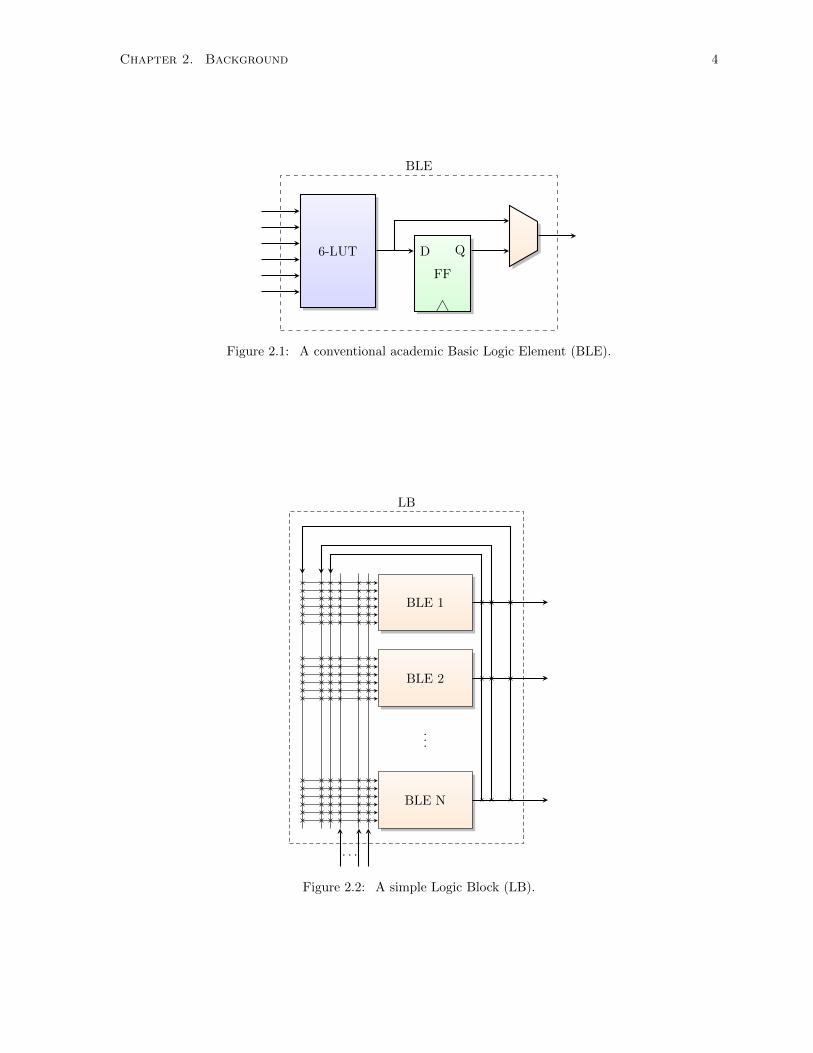
are grouped together into a Basic Logic Element (BLE) (Figure 2.1), where the output of the LUT is
optionally registered. To improve area efficiency and performance, the BLEs are usually grouped together
into a Logic Block (LB) (Figure 2.2) [14, 15, 16].
An FPGA typically consists of columns of LB, with programmable inter-block routing used to
interconnect the LBs as shown in Figure 2.3. The inter-block routing consists of Connection Blocks (CBs)
where adjacent LB input and output pins connect to the FPGA routing, and Switch Blocks (SBs) where
routing wires interconnect (Figure 2.4) [16].
While ‘soft logic’ can be used to implement nearly any type of digital circuit, it may be more efficient
to ‘harden’ certain commonly used functions into fixed-function hardware on the device. This trades-off
flexibility for efficiency. Typical examples of ‘hard’ blocks in modern FPGAs include Digital Signal
3
Chapter 2. Background 4
6-LUT
FF
D Q
BLE
Figure 2.1: A conventional academic Basic Logic Element (BLE).
LB
BLE 1
BLE 2
...
BLE N
. . .
Figure 2.2: A simple Logic Block (LB).

Chapter 2. Background 5
LB
LB
LB
LB
LB
LB
LB
LB
LB
LB
LB
LB
LB
LB
LB
LB
LB
LB
LB
LB
LB
LB
LB
LB
LB
LB
LB
LB
LB
LB
LB
LB
LB
LB
LB
LB
LB
LB
LB
LB
LB
LB
LB
LB
LB
LB
LB
LB
LB
LB
LB
LB
LB
LB
LB
LB
LB
LB
LB
LB
Figure 2.3: A simple homogeneous FPGA.
CB
CB
SB
LB
Figure 2.4: A LB and associated CB and SB. The right-going connections from the horizontal channelare shown with dotted lines.

Chapter 2. Background 6
LB
LB
LB
LB
LB
LB
LB
LB
LB
LB
LB
LB
LB
LB
LB
LB
LB
LB
LB
LB
LB
LB
LB
LB
LB
LB
LB
LB
LB
LB
LB
LB
LB
LB
LB
LB
LB
LB
LB
LB
LB
LB
LB
LB
LB
LB
LB
LB
LB
LB
LB
LB
LB
LB
LB
LB
LB
LB
LB
LB
RA
MR
AM
RA
M
RA
MR
AM
RA
M
RA
MR
AM
RA
M
DS
PD
SP
DS
PD
SP
Figure 2.5: A simple heterogeneous FPGA.
Processing (DSP) blocks (multipliers) and Random Access Memory (RAM) blocks (Figure 2.5). This
variety of block types makes modern FPGAs heterogeneous, an important property which has significant
impacts on the CAD algorithms used to program them.
2.1.2 CAD for FPGAs
In order to program an FPGA to implement a specific application, the designer’s high-level intent
must be translated into a low level bitstream which sets the individual configuration switches in the
FPGA. This translation process constitutes the ‘CAD Flow’. Since the CAD flow takes only an abstract
high-level description, but produces a detailed low level implementation, it must make numerous choices
to implement the system. These choices have very significant impacts on key performance metrics such
as power, area and operating frequency. It is therefore key that the CAD flow makes good choices to
optimize the final implementation.
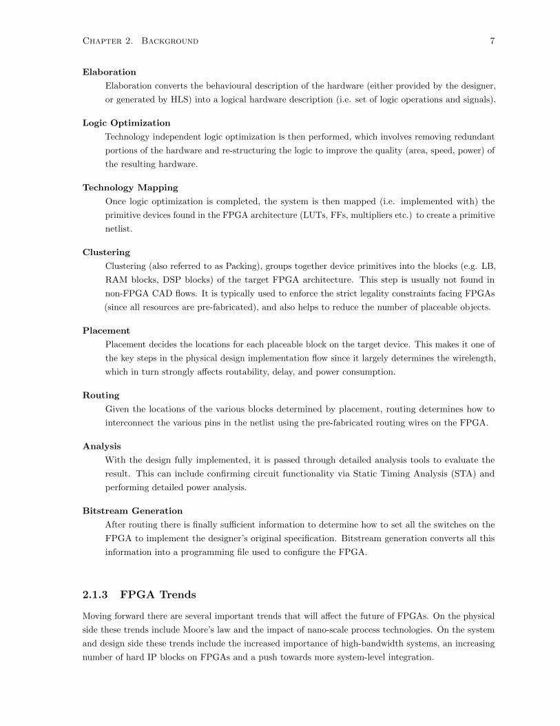
An example FPGA CAD flow is illustrated in Figure 2.6, and discussed below1 [18].
High-Level Synthesis
High-Level Synthesis (HLS) is a relatively recent addition to FPGA CAD flows, which aims to
improve designer productivity by further increasing their level of abstraction. This is typically
accomplished by allowing designers to describe their systems algorithmically, using conventional
programming languages such as C or OpenCL [19, 6, 20], rather than using a close-to-the-metal,
cycle-by-cycle behavioural description using a Hardware Description Language (HDL) (e.g. Verilog,
VHDL). Given an algorithmic description of a system, HLS selects an appropriate hardware
architecture to implement the algorithm.
1It should be noted that while discrete steps in the CAD flow are described here, many modern flows blur the linesbetween these different stages — for example by re-optimizing the design logic after placement [17]. Confusingly, this issometimes referred to as ‘Physical Synthesis’ in the literature. Here we take Physical Synthesis to be an encompassing termfor the physically aware stages of the CAD flow (i.e. packing, placement and routing), in contrast with Logical Synthesiswhich encompasses the non-physically aware stages.
Chapter 2. Background 7
Elaboration
Elaboration converts the behavioural description of the hardware (either provided by the designer,
or generated by HLS) into a logical hardware description (i.e. set of logic operations and signals).
Logic Optimization
Technology independent logic optimization is then performed, which involves removing redundant
portions of the hardware and re-structuring the logic to improve the quality (area, speed, power) of
the resulting hardware.
Technology Mapping
Once logic optimization is completed, the system is then mapped (i.e. implemented with) the
primitive devices found in the FPGA architecture (LUTs, FFs, multipliers etc.) to create a primitive
netlist.
Clustering
Clustering (also referred to as Packing), groups together device primitives into the blocks (e.g. LB,
RAM blocks, DSP blocks) of the target FPGA architecture. This step is usually not found in
non-FPGA CAD flows. It is typically used to enforce the strict legality constraints facing FPGAs
(since all resources are pre-fabricated), and also helps to reduce the number of placeable objects.
Placement
Placement decides the locations for each placeable block on the target device. This makes it one of
the key steps in the physical design implementation flow since it largely determines the wirelength,
which in turn strongly affects routability, delay, and power consumption.
Routing
Given the locations of the various blocks determined by placement, routing determines how to
interconnect the various pins in the netlist using the pre-fabricated routing wires on the FPGA.
Analysis
With the design fully implemented, it is passed through detailed analysis tools to evaluate the
result. This can include confirming circuit functionality via Static Timing Analysis (STA) and
performing detailed power analysis.
Bitstream Generation
After routing there is finally sufficient information to determine how to set all the switches on the
FPGA to implement the designer’s original specification. Bitstream generation converts all this
information into a programming file used to configure the FPGA.
2.1.3 FPGA Trends
Moving forward there are several important trends that will affect the future of FPGAs. On the physical
side these trends include Moore’s law and the impact of nano-scale process technologies. On the system
and design side these trends include the increased importance of high-bandwidth systems, an increasing
number of hard IP blocks on FPGAs and a push towards more system-level integration.

Chapter 2. Background 8
Logical Synthesis
Physical Synthesis
High LevelSynthesis
Elaboration
LogicOptimization
TechnologyMapping
Pack
Place
Route
Analysis
BitstreamGeneration
Figure 2.6: An example FPGA CAD flow.
FPGAs and Moore’s law
The size of the largest FPGAs has followed Moore’s law, roughly doubling in size every 2 to 3 years
(Figure 2.7). This yields great benefits to FPGA designers, as it enables higher levels of integration
(driving down cost, power and increasing performance) while also enabling larger and more complex
systems to be implemented.
Since it is not economically feasible to double the size of an engineering design team every two
years, this puts significant pressure on the design process to improve designer productivity. One way of
accomplishing this is to use automated CAD tools and design flows. However these tools and flows must
also scale well with increasing design size.
Historically some of the CAD tool run-time scalability has resulted from increases in single-threaded
Central Processing Unit (CPU) performance. However, as shown in Figure 2.7, single-threaded CPU
performance has not kept pace with design size, putting more pressure on CAD tools and design flows.
Nano-scale CMOS
Modern process technologies also bring about new design considerations when dealing with nano-scale
Complimentary Metal-Oxide-Semiconductor (CMOS) circuits. These include increasing manufacturing
variability and defects, the breakdown of Dennard (constant field) scaling [21], and the increasing
dominance of interconnect in determining circuit performance [22].
High-Throughput Design
The proliferation of high speed communication interfaces and the large amounts of data they generate
require FPGA systems to support high throughput. There are two general approaches for tackling this
high throughput requirement: widening data paths, or operating at higher speeds. Widening data paths
costs area and often increases critical path delay, since the CAD algorithms can not find equivalent speed

Chapter 2. Background 9
1998 2000 2002 2004 2006 2008 2010 2012 2014
Year
50
100
150
200
250
300
350
400
450
Nor
mal
ized
Val
ue
(199
8)
FPGA Size and SPECInt Over Time
Largest FPGA
Largest Monolithic FPGA
SPECint
Figure 2.7: Design size compared to SPECint CPU performance over time. The large jump in FPGAsize in 2012 is caused by the introduction of interposer-based FPGAs.
solutions. Operating at higher speeds results in tighter timing constraints that become more difficult to
satisfy, requiring increased design effort and time. Modern FPGA families such as Altera’s Stratix 10,
and Achronix’s Speedster22i are built and marketed for high speed designs [23, 24].
Hard IP Blocks
Another trend in modern FPGAs is the growing number of embedded hard Intellectual Property (IP)
blocks. In addition to the standard RAM and multiplier blocks described in Section 2.1.1, other blocks
including hardened memory controllers [23], processor cores [24], and high speed communication protocols
(e.g. PCI-E, Ethernet) [23] are common in modern FPGAs.
System-Level Integration
Similar to ASICs, many FPGA systems are now built up of multiple, largely independent sub-systems. This
has resulted in a System-on-Chip (SoC) design style where IP cores developed by multiple development
teams or by third-parties are integrated into a single system. This facilitates faster design, since design
work on different components can be performed in parallel and later integrated. It also facilitates the
re-use of IP cores across different systems. However, this design style also comes with challenges. In
particular, integration can be difficult and unwanted interactions between different components can be
problematic at late stages of the CAD flow.
2.2 FPGA Benchmarks & CAD Flows
Two of the major thrusts in FPGA research are building improved FPGA architectures (Section 2.1.1)
and improving FPGA CAD tools. Both of these are typically evaluated empirically, since closed form

Chapter 2. Background 10
LogicalSynthesis
BenchmarksArchitecture
PhysicalSynthesis
Analysis
CAD Flow
SatisfactoryResult?
ModifyArchitecture
ModifyCAD Flow
Done
Yes
NoNo
Figure 2.8: CAD and architecture evaluation process.
analytical solutions are rarely applicable. A typical research CAD flow is shown in Figure 2.8. The VTR
project [25] is a popular open-source example of this type of CAD flow. In a research CAD flow a set of
benchmark circuits are mapped onto candidate FPGA architectures, and the results analyzed.
In typical usage for FPGA architecture research, the CAD flow and benchmarks are kept constant
while the target FPGA architectures are varied. Conversely for CAD tool research the benchmarks and
target architectures are kept constant while the CAD flow is varied2. Due to their importance, both
FPGA architectures and CAD tools have been extensively researched. However the third component, the
benchmarks, have been relatively neglected.
2.2.1 FPGA Benchmarks
It is important to ensure that the benchmarks used to evaluate FPGA architectures and CAD flows are
of sufficient scale and complexity, and are representative of modern (and future) FPGA usage. Otherwise,
important issues such as CAD scalability can not be investigated, and the validity of architecture studies
becomes questionable.
The most commonly used FPGA benchmark suites are currently composed of designs that are much
smaller and simpler than current industrial designs. For example, the MCNC20 benchmark suite [26]
released in 1991, has an average size of only 2960 primitives. In comparison current commercial FPGAs
[27] [28] contain up to 2 million logic primitives alone. Furthermore, half of the MCNC benchmarks are
purely combinational, and none of the designs contain hard primitives such as memories or multipliers.
2In reality this distinction is not so clear cut, as there is an interdependence between both the CAD flow and FPGAarchitectures. For example, if a CAD flow fails to take full advantage of an FPGA’s architectural features, or optimizespoorly the conclusions about the architecture would not be accurate.

Chapter 2. Background 11
Automated
Manual
HDL
LogicalSynthesis
PhysicalSynthesis
Analysis
ConstraintsMet?
Done
ModifyDesign
Yes
No
Figure 2.9: FPGA design implementation process.
The more modern VTR benchmark suite [25] is an improvement, but it still consists of designs with
an average size of only 23,400 primitives, which would fill only 1% of the largest FPGAs. Only 10 of
the 19 VTR designs contain any memory blocks and at most 10 memories are used in any design. In
comparison, Stratix V and Virtex 7 devices contain up to 2,660 and 3,760 memory blocks respectively.
The large differences, both in size and design characteristics between current academic FPGA
benchmarks and modern FPGA devices is cause for concern. If the benchmarks being used are not
indicative of modern FPGA usage then the empirical research conclusions made using them may not be
accurate. To ensure research remains relevant, large-scale benchmarks which exploit the characteristics
of modern devices are required. To address these concerns we develop a new FPGA benchmark suite in
Chapter 3.
2.3 Impact of CAD & Design Methodology on Productivity
The typical process for a designer implementing an application targeting an FPGA is shown in Figure 2.9.
A designer describes his/her design using a HDL and then passes it off to the automated CAD flow for
synthesis and analysis. After analysis it is determined whether the design has met its constraints (e.g.
timing, power and area). If the constraints are not satisfied then the designer must go back and modify
their design and re-run the design flow.
Since this iterative process is repeated numerous times during development, it is important that each
iteration occur quickly; however this is rarely the case. Firstly, the synthesis and analysis design flow,
while automated, is large and complex requiring significant computing time — on the order of days for
large designs (Chapter 3). Secondly, manually modifying the design to address the constraint violations
Chapter 2. Background 12
may not be easy. It typically requires design re-verification to ensure correctness is maintained. On large
designs this may involve changes across multiple design components owned by other individuals or teams
— making design modification a time-consuming process3. Given these challenges, it is clear that new
techniques to speed up this process and improve designer productivity are required if we are to continue
designing larger and more powerful computing systems.
2.3.1 Scaling Challenges and Approaches
There are two primary approaches to improving designer productivity:
1. Reducing the required number of design iterations, and
2. Reducing the required time for each design iteration.
Timing closure, the process of modify the design or CAD tool settings until all timing constraints are
satisfied, is responsible for a large number of design iterations, particularly at late stages of the design
process. Therefore identifying ways to reduce the number of iterations required to close timing would be
a significant productivity boost. Section 2.4 discusses timing closure in detail and describes techniques
which can be used to address it.
Within each design iteration a significant amount of time is spent modifying and synthesizing the
design. Section 2.5 discusses the techniques that have been used to speed-up design modification and
synthesis. It also identifies floorplanning, a divide-and-conquer approach, as a technique which could be
applied to speed-up the synthesis process. Section 2.6 formally defines the floorplanning problem while
Section 2.7 and Section 2.8 describe previous work on floorplanning for ASICs and FPGAs.
2.4 Timing Closure
One of the most difficult constraints to satisfy during the design of an FPGA system are the timing
constraints, which ensure the circuit operates correctly and at the expected speed. The two primary
timing constraints designers are concerned about are the setup and hold constraints. Both of these
constraints must be satisfied for a synchronous digital circuit to avoid metastability and function correctly.
Setup constraints ensure that signals arrive at registers a sufficient amount of time before the capturing
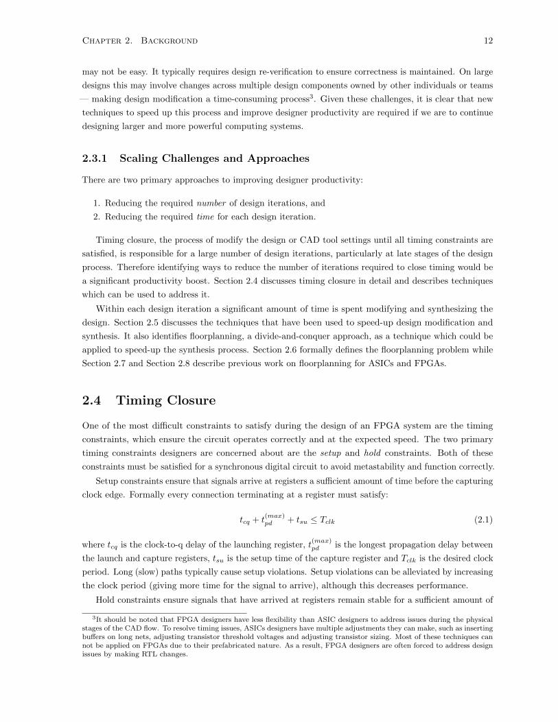
clock edge. Formally every connection terminating at a register must satisfy:
tcq + t(max)pd + tsu ≤ Tclk (2.1)
where tcq is the clock-to-q delay of the launching register, t(max)pd is the longest propagation delay between
the launch and capture registers, tsu is the setup time of the capture register and Tclk is the desired clock
period. Long (slow) paths typically cause setup violations. Setup violations can be alleviated by increasing
the clock period (giving more time for the signal to arrive), although this decreases performance.
Hold constraints ensure signals that have arrived at registers remain stable for a sufficient amount of
3It should be noted that FPGA designers have less flexibility than ASIC designers to address issues during the physicalstages of the CAD flow. To resolve timing issues, ASICs designers have multiple adjustments they can make, such as insertingbuffers on long nets, adjusting transistor threshold voltages and adjusting transistor sizing. Most of these techniques cannot be applied on FPGAs due to their prefabricated nature. As a result, FPGA designers are often forced to address designissues by making RTL changes.

Chapter 2. Background 13
1(130nm)
2(90nm)
3(65nm)
4(40nm)
5(28nm)
Stratix Device Generation
100
150
200
250
300
350
400
450
500
Fm
ax[M
Hz]
Frequency Crossing Regions ofEquilvalent LEs Across Device Generations
40K LEs
79K LEs
179K LEs
338K LEs
813K LEs
Max LEs
Figure 2.10: Achievable register to register operating frequency across regions containing an equivalentnumber of Logic Elements (LEs) for Stratix devices; measured with Altera’s Quartus II.Max LEs corresponds to the largest device available each generation.
time after the capturing clock edge. Formally:
tcq + t(min)pd ≥ th (2.2)
Where tcq is the clock-to-q delay of the upstream register, t(min)pd is the shortest propagation delay between
the upstream and current register, and th is the required hold time of the current register. Short (fast)
paths typically cause hold violations. Unlike setup violations, hold violations can not be fixed by changing
the clock frequency.
Satisfying all these constraints is very time consuming, and typically requires many iterations of the
design cycle in Figure 2.9. Furthermore, since timing closure occurs late in the design process (as part of
a final design sign-off), the design is otherwise complete and difficult timing closure can delay going into
production. Coupled with the relatively poor predictability of the timing closure process (the iterative
flow may have difficulty converging) it is often a critical stage in the entire design process.
Timing closure has always been an important and time consuming process, but it is becoming
more challenging. The trend towards high-throughput design is pushing up clock frequency targets,
while modern nano-scale CMOS is introducing new challenges for high speed design (Section 2.1.3). In
particular, the different scaling characteristics of devices, local interconnect, and global interconnect [22]
in modern process technologies are making it more difficult to achieve timing closure in a predictable and
timely manner.
The difference in scaling between local and global interconnect4 is illustrated for FPGA devices
in Figure 2.10. This shows that the speed of local communication within a relatively small amount
of logic (i.e. 40K LEs) has more than doubled over five generations. In contrast, the speed of global
4This is particularly important for FPGAs where interconnect already contributes significantly to overall delay.

Chapter 2. Background 14
communication across the full device (i.e. Max LEs) has degraded. This growing mismatch between local
and global communication speed makes it increasingly difficult to close timing on large designs.
2.4.1 Scalability Challenges with Synchronous Design
The constraints involved in timing closure are derived from the conventional synchronous design style,
which is the dominant paradigm for digital design. Synchronous design has been very successful,
largely due to its amenability to design automation, simple conceptual model and flexibility. However,
synchronous design is also restrictive, enforcing the synchronous assumption — that both computation
and communication (e.g. between two registers) must occur within a single clock cycle. On modern
devices, where it may take multiple clock cycles to traverse the chip, this can be too restrictive.
One solution to the interconnect scaling problem is to insert pipeline registers on communication links
that traverse large portions of the chip. This breaks the link into shorter segments which can operate at
higher speed, and allows multiple clock cycles for the signal to propagate.
The problem with this solution is that it modifies the latency of the communication link. This changes
the Register Transfer Level (RTL) behaviour of the system, requiring the re-design and re-verification of
the system’s control logic. Furthermore, the impact of these RTL changes are not known until after the
time consuming physical design flow (which may take multiple days [29]) has been completed, making
this a slow and iterative process. Furthermore, critical timing paths may move, or new paths may appear,
requiring the whole process to be repeated with no guarantee of convergence. This tight coupling between
communication latency and system behaviour significantly complicates any divide-and-conquer design
approaches since it introduces interdependencies between components.
2.4.2 Beyond Synchronous Design
Given the inherent assumptions and limitations of synchronous design, many alternative design styles
have been proposed. The key challenge with these design styles is balancing the resulting design flexibility
against the difficulty of designing such systems. In particular ensuring that designers can easily reason
about the correctness of their systems and successfully automate the design process are important
considerations. The following sections discuss several proposed alternative design styles.
Alternative 1: Wave-Pipelining
In a conventional synchronous system each data bit transmitted along a wire must be latched by a clocked
storage element before the following bit is launched. With wave-pipelining, multiple data bits are allowed
to be in flight along the same wire. This allows the interconnect to behave as if pipelined — with the
wire itself storing the multiple data bits in flight rather than registers, potentially saving the area, power
and timing overhead of using registers. It was shown in [30] that wave-pipelined interconnect could be
used in an FPGA.
Wire-pipelining however, does not avoid the problem of re-designing a system’s control logic to account
for the additional communication latency, and also introduces further design issues. Since no stable
storage element is used to separate the multiple bits transmitted along a wire, wave-pipelining systems
must be meticulously designed to ensure correct operation and avoid interference between subsequent
bits. One challenge for these systems is that they can not be run at lower speeds, which makes debugging
difficult. This undesirable behaviour is caused by tying the latency of a wave-pipelined link to the

Chapter 2. Background 15
(constant) delay of a wire, rather than to the number of registers. As a result, the effective latency of a
wave-pipelined link changes with clock frequency. Additionally, wave-pipelining systems must operate
robustly in the presence of die-to-die and on-chip variation, as well as in the presence of crosstalk and
power supply noise [30]. These non-idealities are expected to become more significant in future process
technologies, and the flexibility of FPGAs would make verifying such systems difficult.
Wave-pipelining does not resolve the problem of re-designing control logic, introduces additional
limitations to system behaviour, and increases design complexity. As a result, wave-pipelining fails to be
a practical solution.
Alternative 2: Asynchronous Design
Asynchronous design has long been touted as an alternative to synchronous design. Under this design
methodology no clock is used to enforce globally synchronized communication. Instead components of
the design detect when their inputs are valid and only then compute their results.
However, despite decades of research, asynchronous design methodologies have seen limited adoption.
The reasons for this include a lack of CAD flows and tools to implement and verify designs, the difficulty
designers have reasoning about the correctness of their systems, and the challenges of testing asynchronous
devices [31].
Alternative 3: Globally Asynchronous Locally Synchronous Design
Another alternative design methodology is Globally Asynchronous Locally Synchronous (GALS). In this
methodology small sub-modules are designed synchronously, but global communication between modules
occurs asynchronously, typically through a wrapper module. This allows timing paths to be isolated
within each sub-module easing timing closure. Furthermore, since smaller more localized clocks with
lower skew are used, this may help to improve performance and power.
One of the key challenges in any GALS design methodology is avoiding metastability when transferring
data between sub-modules, since their clocks are no longer synchronous. Several different GALS design
styles have been proposed to address this issue [32, 33]. One approach is based on pausable clocks,
where each sub-module has a locally generated clock which is paused before data arrives to ensure
that metastability is avoided. Alternately, GALS can be implemented using asynchronous First-Input
First-Outputs (FIFOs) to handle communication between sub-modules. Additionally in some cases,
where the relationships between sub-module clocks are known, conventional flip-flop based synchronizers
can be used.
On current FPGAs, it is not possible to locally generate clocks for sub-modules as would be done on
an ASIC. As a result these clocks would have to be centrally generated (with a PLL/DLL) and distributed
to the local sub-modules. FPGAs typically contain a relatively small number of fixed clock networks,
consisting primarily of global, and large regional/quadrant clock networks. Since these clock networks
are pre-fabricated, there is not much to gain (in terms of skew and power) by using them to distribute
small clocks. This is different from an ASIC where custom smaller clock trees can be designed. While
FPGAs do also support some smaller fixed clock networks, these are typically quite small (limiting the
size of sub-modules), restrict placement flexibility, and may be difficult to reach from clock generators.
While it is possible to distribute clocks with the regular inter-block routing, it is undesirable. The
inter-block routing network is not designed for clock distribution, lacking shielding (increasing jitter),
Chapter 2. Background 16
and having unbalanced rise-fall times which may distort the clock waveform. Such a clock network would
also consume more power and typically have more skew than an equivalent fixed clock network.
GALS also faces problems similar to fully asynchronous design for the asynchronous portions of
the system, including difficulty implementing, verifying and testing such systems. While CAD flows
for GALS design are perhaps better developed than for fully asynchronous design, they still require
substantial design knowledge and manual intervention [34]. These challenges make adopting a GALS
design methodology for FPGAs quite disruptive.
Alternative 5: Re-timing
Another design style to consider is a modified synchronous methodology, making use of re-timing [35].
Under this methodology CAD tools are allowed to move pipeline registers around logic, provided they
do not change the observable I/O behaviour of the system. This is primarily helpful only for circuits
with poorly balanced pipeline stages, and as a result often offers limited improvement on typical FPGA
designs [36].
Re-timing can be extended in two ways, by allowing additional registers to be added to the circuit.
The first is re-pipelining, where additional registers are added to the I/Os of the circuit and then re-timing
is performed. While this gives extra registers for the re-timer to improve the balance between stages, it is
limited to circuits which have no dependencies on previous computations (i.e. are strictly feed-forward).
The second technique is C-slowing, where C additional registers are inserted for every original register in
the design before re-timing is performed. This allows more general classes of circuits, such as those with
feedback, but may not be suitable for all designs since it forces C independent threads of computation to
be used.
Alternative 6: Latency Insensitive Design
LID [37] can be viewed as a middle ground between the synchronous and asynchronous design method-
ologies, where design components are insensitive to the latency of the communication between them. It
breaks the synchronous assumption, but does not go so far as to totally remove global synchronization.
This means that while communication is still synchronized to a clock at the physical level, it may take
multiple clock cycles for communication to occur in the designer’s RTL description.
This yields additional flexibility during the design implementation process compared to synchronous
design, but is more tractable than asynchronous design. Keeping communication synchronous at the
physical level means conventional synchronous CAD flows and tools can be used to implement designs,
and designers can still reason about the correctness of their systems from the perspective of timing
constraints. Additionally, emerging FPGA communication styles such as embedded NoCs [38, 39] result
in variable latency communication, requiring designs to be latency insensitive. LID also does not require
modification of existing FPGA architectures, as would be required to fully support wave-pipelining [30],
asynchronous[40], or GALS [41] design styles.
2.4.3 Latency Insensitive Design
Of the alternatives discussed above, LID appears to be particularly promising. LID enables enough
flexibility to the design process to address the timing closure challenges associated with synchronous

Chapter 2. Background 17
Pearl B
Pearl C
Pearl A
(a) Logical system connectivity.
FPGA
RS
RS
Pearl B
Shell
Pearl C
ShellPearl A
Shell
RS
(b) Latency insensitive system implementation, showingshells and inserted relay stations (RS).
Figure 2.11: Latency insensitive system example.
design. However it is sufficiently similar to the synchronous approach that existing FPGA architectures
and design tools can still be used.
One of the key use cases for LID is the pipelining of communication links which (since the links
are latency insensitive) does not change the correctness of the design. This is significantly different
from conventional synchronous design, and makes the process of inserting pipeline registers to address
timing closure issues amenable to design automation. LID may also help abstract a design from the
implementation details of the underlying FPGA, potentially enhancing the timing and performance
portability of designs when re-targeting to larger or newer FPGAs. Latency insensitivity could also be
beneficial for FPGA architectures featuring pipeline registers embedded in the routing fabric [42, 43].
The formal theory of latency insensitive design [37] shows that any conventional synchronous system,
typically called a pearl, can be transformed into a latency insensitive system, provided it is stall-able5.
This is accomplished by placing the pearl in a special (but still synchronous) wrapper module, typically
called a shell. The theory further shows that such wrapped modules can be composed together, and the
latency of communication links between them varied, by inserting relay-stations (analogous to registers),
without affecting the correctness of the overall system. The resulting system is guaranteed to be dead-lock
free [37].
An example system is shown in Figure 2.11. The logical system, as described by an RTL de-
signer, is shown in Figure 2.11a. After implementation with a latency insensitive CAD flow the design
implementation may appear as in Figure 2.11b.
The scheme described above (and in additional detail in Section 4.2) implements dynamically scheduled
LID, where the validity of a module’s inputs are determined dynamically at run time by the shell logic.
Statically scheduled LID schemes have also been proposed [44], which determine when inputs are valid at
design time before implementation. As a result, statically scheduled LID has reduced overhead (the shells
are much simpler), but it severely limits the flexibility of the system implementation. For example, it
significantly restricts any potential CAD optimizations, such as automated pipelining, and also precludes
operation with variable latency interconnect such as an NoC.
One potential concern with a latency insensitive system is the impact of stalling (caused by back-
5Informally, capable of maintaining its state independent of its current inputs (i.e. no combinational connections frominputs to outputs). See [37] for a formal definition.
Chapter 2. Background 18
pressure) on system throughput. As shown in [45] stalling can reduce throughput in systems containing
cycles of latency insensitive links. In particular [45] showed that inserting relay stations in ‘tight’ cycles
degrades throughput more than in inserting them in ‘loose’ cycles. As a result any CAD tool which
aims to automatically insert relay stations to address timing issues should also consider the impact on
throughput. The potential impact on throughput can also be reduced (but not eliminated) by increasing
the amount of buffering within shells as shown in [46].
An interesting question is what level of granularity is appropriate for latency insensitive communication.
While it is possible to use latency insensitive communication at a very fine level, this is not necessarily
required. As shown in Figure 2.10, local communication can still occur at high speed. The problem is
long distance (global) communication. As a result it may make sense to implement latency insensitive
communication at a coarse level that captures primarily global communication.
Some previous work has looked at latency insensitive communication in FPGA-like contexts. In
[47], explicit latency insensitive communication was used to improve the design and implementation of
multi-FPGA prototyping systems. The authors of [48] proposed an elastic Coarse-Grained Reconfigurable
Array (CGRA) architecture exploiting latency insensitive communication to avoid static scheduling,
and to allow simpler translation of high level languages (i.e. C) into circuits. For their system, which
implements latency insensitive communication for each ALU element, they identify the area and delay
overhead of their elastic CGRA (compared to an inelastic CGRA) as 26% and 8% respectively. The work
presented in [49] describes an FPGA overlay architecture that uses latency insensitive communication.
The authors report area overheads (compared to a baseline system) of 3.4× and 10.6× for a floating
point and integer based overlay respectively. The high overheads can be attributed to the additional
routing flexibility required for the overlay, and the use of fine-grained latency insensitive communication.
Our study of LID in Chapter 4 differentiates itself from the above by focusing on the overheads of
using latency insensitive communication for RTL designs targeting conventional FPGAs, rather than as
part of an overlay layer or hardened into the device architecture.
2.5 Scalable Design Modification and Synthesis
The constantly increasing design sizes that have resulted from following Moore’s Law (Section 2.1.3)
makes producing scalable design flows an essential part of improving designer productivity.
2.5.1 Scalable Design Modification
One set of approaches has focused on making it easier for designers to describe and modify their high
level system descriptions. Techniques that fall into this area include HLS and more productive design
languages such as BlueSpec [50]. While these techniques can be effective at reducing the amount of
time required to make changes to large complex designs, they do not eliminate the need altogether.
Additionally, by providing a more abstract description to manipulate, it may no longer be obvious to the
designer what needs to be changed to address a low level physical problem.
2.5.2 Scalable Design Synthesis
Design synthesis, particularly the physical design implementation (i.e. packing, placement, and routing),
while heavily automated, is a significant computational problem. As a result it may takes days for this

Chapter 2. Background 19
process to complete on large designs (Chapter 3). Many approaches have been used to help reduce this
time.
Perhaps the most successful approach has focused on developing improved algorithms that produce
better results and reduce execution time. While this approach has been fruitful, it is ad-hoc and difficult
to predict if or when improved algorithms will be found.
Another set of approaches have focused on developing parallel CAD algorithms. These aim to
exploit the multiple cores available on modern processors to speed-up their algorithms. While numerous
algorithms have been proposed, their scalability has often been limited without quality loss [51, 52, 53].
The speed-up of parallel CAD has often been limited for several reasons. First, digital circuits often have
complex inter-dependencies which make it difficult to extract parallelism. Second, many of the most
successful CAD algorithms (e.g. Simulated Annealing (SA) and PathFinder routing) are iterative, relying
on making incremental changes to the state of the system (Figure 2.14). This creates dependencies
between actions, limiting the available amount of parallelism.
An alternative approach which has not been well studied on FPGAs is to change the nature of the design
implementation by explicitly partitioning it into separate independent parts. This divide-and-conquer
approach is typically referred to as floorplanning.
2.5.3 Floorplanning
Initially we clarify our terminology for logical partitions (Definition 1) and physical regions (Definition 2).
Definition 1 (Logical Partition)
A logical partition, pi, is a set of netlist primitives. Each netlist primitive in a circuit is assigned to a
single logical partition.
Definition 2 (Physical Region)
A physical region, ri, is the part of chip contained within some closed boundary.
In typical usage each partition pi is assigned to a single region ri.
A floorplanning design flow involves two steps which are not found in the conventional design flow
(Figure 2.6): design partitioning and floorplanning. Figure 2.12 illustrates how such a divide-and-conquer
design flow may be structured. Design partitions can either be generated automatically by a partitioning
tool, or provided by a designer. Floorplanning then allocates a unique region on the target substrate6 for
each logical design partition as shown in Figure 2.13. Floorplanning yields several advantages to the
design process.
Firstly, it spatially decouples the physical design implementation of the partitions. This enables the
design implementation of the components to be performed in parallel. In the context of team-based
design this allows multiple teams to work on different sub-components of a design independently. In the
context of an automated design implementation flow, it allows each component to be packed, placed and
routed independently without the fine-grained synchronization overhead found in parallel algorithms7,
speeding up the process. Additionally spatial decomposition prevents the physical design tools from
optimizing across partition boundaries. From one perspective this can be advantageous, as it allows the
6a silicon die for an ASIC, or a specific device for an FPGA7That is to say, floorplanning allows the exploitation of process-level parallelism across partitions. The actual implemen-
tation of each component could still be performed using parallel algorithms, yielding further speed-up.

Chapter 2. Background 20
Logical Synthesis
Physical Synthesis
High LevelSynthesis
Elaboration
LogicOptimization
TechnologyMapping
Automated/UserPartitioning
Floorplan
Pack
Place
Route
Analysis
BitstreamGeneration
Figure 2.12: An example floorplanning CAD flow.
tools to focus on each region independently and prevents unwanted interactions across region boundaries8.
From another perspective it is disadvantageous, as it prevents potentially beneficial optimizations from
occurring across region boundaries.
Secondly, it enables early design feedback and enables a more predictable design methodology. Since
the floorplanning process occurs early in the design flow, it becomes one of the first stages to get a
physically aware view of the design. This enables it to provide feedback on the system level characteristics
of a design, such as long distance timing critical connections. It additionally provides constraints to
downstream tools which, if they are met, will ensure the design functions correctly. This yields a more
structured and predictable design methodology.
While floorplanning is a common stage in many large-scale ASICs CAD flows, it is not widely used
in FPGA CAD flows. Historically this has been due to the large design sizes found in ASICs, which
exceed the capacity of automated design tools, and also the desire for a controlled and predictable design
cycle which is required to handle the complex design issues found in ASIC design (clock-tree synthesis,
scan insertions, cross-talk, IR drop etc.). These factors favour a floorplanning flow which partitions the
design and allows the components to be implemented independently, verified independently, and finally
integrated. In contrast, their smaller design sizes and higher level of abstraction from some of the detailed
physical considerations has meant floorplanning has traditionally been avoided in FPGA CAD flows.
8For example, this can prevent downstream CAD tools from mixing the physical implementations of seperately designedIP cores, an important consideration for the modern SoC design style where many seperately designed IP cores are integratedinto a single system (Section 2.1.3).

Chapter 2. Background 21
Partitioned Netlist
r 4
r 3
r 2
r 1
r 0
Target Substrate
p0 p1 p2 p3 p4
Figure 2.13: Floorplan for a partitioned netlist.
2.6 Types of Floorplanning Problems
While we have given an overview of floorplanning, it is useful to formally define the floorplanning problem
and differentiate between its variations.
2.6.1 The Homogeneous Floorplanning Problem
The conventional floorplanning problem involves finding non-overlapping physical regions where each
region has sufficient area and some objective function is optimized9.
Let R be a set of N regions (i.e. a floorplan), where ri corresponds to the ith region. Let each
region ri be associated with a logical partition pi. Let A(ri) be the area of region ri, and Ai be the
minimum area required to implement partition pi. Let f(R) be the cost of a specific floorplan. Then the
homogeneous floorplanning optimization problem is defined as:
minimizeR
f(R)
subject to A(ri) ≥ Ai ∀i ∈ Nri ∩ rj = ∅ ∀i, j ∈ N | j 6= i.
(2.3)
The goal of (2.3) is to minimize the cost function with a valid solution satisfying the constraints.
The first set of constraints, A(ri) ≥ Ai, ensure that each region has a sufficient area (Ai) to implement
partition pi. The second set of constraints, ri ∩ rj = ∅, ensure that regions are non-overlapping. The
homogeneous floorplanning problem has been shown to be NP-hard [54, 55].
9Since only a single resource (area) is considered, we refer to this as the Homogeneous Floorplanning Problem. In generalthe single resource may not even be area.

Chapter 2. Background 22
2.6.2 The Fixed-Outline Homogeneous Floorplanning Problem
Another variation of the floorplanning problem occurs when a fixed-outline constraint is applied. The
fixed-outline homogeneous floorplanning problem is:
minimizeR
f(R)
subject to A(ri) ≥ Ai ∀i ∈ Nri ∩ rj = ∅ ∀i, j ∈ N | j 6= i
ri ⊆ θmax ∀i ∈ N.
(2.4)
Where the new constraints in (2.4), ri ⊆ θmax, ensure every region ri is contained within the fixed outline
θmax.
2.6.3 The Rectangular Homogeneous Floorplanning Problem
It is common to assume that each region ri is rectangular with width wi, height hi, and an aspect ratio
AR(ri) = wi/hi. The rectangular homogeneous floorplanning problem is then:
minimizeR
f(R)
subject to A(ri) ≥ Ai ∀i ∈ Nri ∩ rj = ∅ ∀i, j ∈ N | j 6= i
γmini ≤ AR(ri) ≤ γmaxi ∀i ∈ N.
(2.5)
The additional constraints, γmini ≤ AR(ri) ≤ γmaxi , in (2.5) restrict each region’s aspect ratio to fall
within the inclusive range [γmini , γmaxi ]. Limiting the range of aspect ratios may be desirable, as regions
with extreme aspect ratios may either be impossible to implement (e.g. the region is, or contains, a fixed
dimension macro), or may result in a poor quality implementation10.
2.6.4 The Heterogeneous Floorplanning Problem
The heterogeneous floorplanning problem is a generalized version of the homogeneous floorplanning
problem, that considers multiple types of resources. Indeed, the homogeneous floorplanning problem can
be viewed as a special case of the heterogeneous problem which only considers a single resource type
(area). Consequently the heterogeneous floorplanning problem is also NP-hard.
To simplify the discussion we define resource vectors (Definition 3) and their comparison (Definition 4)
as in [56].
Definition 3 (Resource Vector)
φ = (n1, n2, . . . , nk) is a resource vector of k resource types. Each ni is the amount of resource type i
associated with the resource vector.
Definition 4 (Resource Vector Comparison)
φ ≤ φ′ iff n1 ≤ n′1 ∧ n2 ≤ n′2 ∧ · · · ∧ nk ≤ n′k, where φ = (n1, n2, . . . , nk) and φ′ = (n′1, n′2, . . . , n
′k) are
resource vectors containing the same resource types.
10In an ASIC or FPGA context extreme aspect ratios can increase wirelength, since the maximum distance betweenplaced netlist primitives tends to increase. It can also exacerbate routing congestion, since most signals would run in eitherthe vertical (AR � 1.0) or horizontal (AR � 1.0) direction.

Chapter 2. Background 23
The other comparison operators follow from Definition 4.
We can now discuss resource requirements for netlist partitions, and resource availability of a region
in terms of resource vectors. Let φ(ri) be the resource vector of region ri, and φi be the resource vector
required to implement partition pi. The heterogeneous floorplanning problem can then be defined as:
minimizeR
f(R)
subject to φ(ri) ≥ φi ∀i ∈ Nri ∩ rj = ∅ ∀i, j ∈ N | j 6= i.
(2.6)
Equation (2.6) is similar to the homogeneous floorplanning problem (2.3), with the key difference that
resource vectors are now compared, rather than scalar values. It is also worth noting that the constraints
ri ∩ rj = ∅ in this more general form can be interpreted as enforcing that all regions contain independent
resources, rather than simply preventing overlap between regions as in (2.3). The fixed-outline and
rectangular region extensions are similar to (2.4) and (2.5).
2.6.5 Optimization Domain
Another consideration for any optimization problem is the optimization domain being considered, which
can have a significant impact on what optimization techniques can be applied. The optimization domain
characterizes the nature of the solution space, which is typically classified as being either continuous or
discrete. A problem with a continuous optimization domain has an infinite set of potential solutions. A
problem with a discrete optimization domain has only a finite set of potential solutions. Optimization
problems with a discrete domain are often referred to as combinatorial optimization problems, since they
involve finding the best combination of variables selected from the finite set of potential values.
The nature of an optimization domain can have a significant impact on what types of optimization
techniques are available. For instance some optimization techniques (such as conjugate gradient methods)
can only be applied to problems with continuous optimization domains. While a problem may natively be
either continuous or discrete, it is often possible to formulate a similar problem in a different domain. For
instance a continuous problem can be transformed into a discrete problem by only considering a subset
of the potential solutions. While such transformations may enable the use of other solution techniques,
the solution found may not be optimal since the transformed problem may not accurately reflect the
original problem.
ASIC floorplanners generally operate in the continuous domain11, while FPGA floorplanners operate
in the discrete domain.
2.7 Floorplanning for ASICs
There has been extensive research into floorplanning for ASICs. This section reviews some of the prominent
techniques and floorplan representations that have been studied. While many of these techniques may
not be directly applicable to FPGAs floorplanning they introduce many important concepts and ideas
that can be applied.
11The assumption of continuity in ASIC floorplanning is actually an approximation. Modern manufacturing processesenforce minimum dimension and spacing rules, which mean the boundaries of regions (and hence their areas) are not trulycontinuous.

Chapter 2. Background 24
The ASIC floorplanning problem is a case of the homogeneous floorplanning problem (Equation (2.3)),
with area being the single resource type considered. In most academic research the rectangular region
assumption is usually made, focusing on the rectangular homogeneous floorplanning problem (Equa-
tion (2.5)). Modules with fixed aspect ratios (γmini = γmaxi ) are typically referred to as ‘hard modules’
(since their shapes can not be changed), while modules with variable aspect ratios (γmini 6= γmaxi ) are
referred to as ‘soft modules’ (since their shapes can be changed)12.
Historically, it has been assumed that during the floorplanning process the size of the final floorplan
(i.e. bounding box of all regions) is variable, and is one of the key metrics to minimize. However, the
variable die-size assumption may not hold for modern ASICs where the dimensions of the die may be
fixed early in the design process due to other constraints such as Input/Output (I/O) pins [54]. The
introduction of a fixed-outline constraint introduces new considerations to floorplanning, namely how (or
if) to handle illegal solutions which extend beyond the outline.
There are several metrics typically used to evaluate the quality of a specific floorplan including:
Region Area The total area of all regions in the floorplan.
Bounding Box Area The area of the floorplan bounding box.
Dead-space The difference between the bounding box and region areas, often expressed as a percentage
of the bounding box area.
Half-Perimeter Wirelength An approximate measure of the wiring requirements between each region.
Timing An approximate measure of the timing quality usually obtained by STA [57].
These terms are often combined to form an objective function for the optimization problem presented in
Section 2.6.
2.7.1 ASIC Floorplanning Techniques
Automated floorplanning has been well studied for ASICs, with a wide range of approaches being
presented in the literature13.
Most ASIC floorplanning techniques can be classified into two categories, those based on analytic
formulations, which make use of mathematical techniques such as linear programming and convex
optimization, and those based on iterative refinement algorithms such as simulated annealing.
Analytic ASIC Floorplanning Techniques
One of the early analytic floorplanning techniques presented formulated the problem as a Mixed-Integer
Linear Programming (MILP) problem [60]. The authors show that it is possible to model both soft and
hard blocks, as well as wirelength and timing requirements by linearizing non-linear constraints and
objective functions. However, the scalability of MILP techniques is limited by its worst-case run-time
which grows exponentially with the number of integer variables. To resolve this, they use a successive
augmentation approach where small sub-problems are solved (optimally) and then combined to build up
a final solution.
A more recent analytic floorplanning technique used in a fixed-outline context is presented in [61].
Here the authors perform an initial rough floorplanning using techniques similar to those used in analytic
12This is different from the terminology used in FPGA architecture research where ‘hard’ and ‘soft’ refer to whether logicis implemented in the programmable fabric, or as fixed-function hardware embedded in the device architecture.
13For detailed overviews see [58] and [59].

Chapter 2. Background 25
State
Modify State
Evaluate State
Accept State?
Update State Revert State
Finished?
Done
Yes
No
Yes
No
Figure 2.14: Iterative improvement algorithm.
placement. They use conjugate gradient methods (i.e. convex optimization) to minimize a quadratic
wirelength model, while attempting to achieve a uniform distribution of modules within the fixed-die and
minimize overlap between modules. Using the relative placement of these modules they formulate and
solve another problem using the conjugate gradient method to re-size any flexible modules to minimize
overlap. Finally a greedy overlap remove algorithm is used to legalize the minimally overlapped floorplan.
This algorithm is shown to be more scalable than the Parquet-4 SA based floorplanner — requiring less
run-time on designs with over 100 modules, while producing better result quality. However, the reliance
on soft-module resizing to help ensure legality may cause the algorithm difficulty when applied to designs
with fixed or restricted module aspect ratios [58].
Iterative Refinement ASIC Floorplanning Techniques
Iterative refinement algorithms, are very popular for ASIC floorplanning. These algorithms typically
follow the general method shown in Figure 2.14. They start with some initial configuration (state) which
defines the geometric relationship between the different partitions. This configuration is then modified in
some manner to create a new configuration. The new configuration must then be converted into an actual
geometric floorplan, where each partition is allocated a region with a specific location and dimensions.
The conversion process from configuration to floorplan is often called ‘realization’, or ‘packing’. The
floorplan is then evaluated using some cost function, and the result used to either accept or reject the
new configuration. This process repeats until some exit criteria is met.

Chapter 2. Background 26
By far the most widely studied algorithm for floorplanning is SA, although other iterative techniques
such as evolutionary algorithms have also been investigated [62, 63].
2.7.2 Simulated Annealing
SA is a general optimization technique based on an analogy to the physical process of annealing materials.
In the physical case, a material such as a metal is heated to a high temperature (energy) state, and then
allowed to slowly cool. In the initial high energy state there is significant freedom for the atoms in the
material to move between energy states. However as the system cools the probability of an atom moving
to a higher energy state decreases, biasing the system to settle into a low energy state.
In the case of SA an algorithm (Algorithm 1) is used to simulate this process. To perform SA the
algorithm explores solutions in the ‘neighbourhood’ of the current solution. Neighbouring solutions are
generated by perturbing the current solution, a process often referred to as a ‘move’. Once a neighbouring
solution has been generated, its cost is evaluated and compared to the cost of the current solution. Most
annealing implementations accept moves following the metropolis criteria [64]:
• Downhill moves which have a lower cost than the current solution are always accepted.
• Uphill moves which have increased cost are accepted with probability e−δc/T .
The metropolis criteria mean that moves with larger cost increases (large δc) are exponentially less
likely to be accepted. The temperature parameter T allows the directedness of the search process to be
controlled. At high temperatures almost any move is accepted, so the annealer randomly searches the
solution space. As the temperature falls the search gains directedness, favouring moves that decrease cost
while still accepting some that increase cost; at sufficiently low temperatures only downhill moves are
accepted. One of the key elements of SA’s success is its ability to hill climb (accept moves which increase
cost). This allows SA to escape from local optima (situations where all local moves appear to be uphill)
in hopes of finding a better solution.
Algorithm 1 Simulated Annealing
Require: Sinit an initial solution1: function Simulated-Anneal(Sinit)2: T ← init-temp(Sinit) . T is the current temperature3: S ← Sinit . S is the current solution4: repeat5: repeat6: Snew ← perturb-solution(S) . Snew is a neighbouring solution7: δc ← cost(Snew)− cost(S) . δc is the difference in cost8: if δc < 0 then . Always accept downhill moves9: S ← Snew
10: else if probabalistic-accept(δc, T ) then . Sometimes accept uphill moves11: S ← Snew12: until inner stop criteria satisfied13: T ← update-temp(T )14: until outer stop criteria satisfied15: return S
SA is a very flexible algorithm, and as a result there are a variety of key parameters and characteristics
that must be determined including the:
Chapter 2. Background 27
Initial Solution: how the initial solution (Sinit) is found.
Initial Temperature: how the initial temperature is chosen.
Solution Representation: how the solution space is represented.
Move Generation: how neighbouring solutions are generated from the current solution.
Cost Function: how solutions are evaluated, which guides the search process.
Acceptance Criteria: how moves are accepted or rejected
Temperature Schedule: how the temperature is updated.
Inner-Loop Exit Criteria: how many moves to make between temperature updates.
Outer-Loop Exit Criteria: how to determine when to terminate the annealing process.
The adaptability of simulated annealing has made it a popular choice for a wide range of optimization
problems. In particular it places few restrictions on the cost function, which does not have to be linear
or convex, and may even be calculated numerically (rather than analytically derived from the solution
representation). Furthermore, the solution representation and move generation can be created in such a
way to make traversing the solution space more efficient or effective. For instance, legal solutions can be
guaranteed by generating a legal initial solution and ensuring the move generator produces only legal
moves.
However, SA is not without its drawbacks. While SA has been proved to be capable of finding globally
optimal solutions, guaranteeing this is computationally prohibitive due to the slow cooling rate required
[65]. Even giving up on globally optimal solutions, SA often does not scale as well as other techniques on
large problem sizes [61].
2.7.3 Floorplan Representations
Most work on SA for floorplanning has focused on the solution representation and associated move
generation. As a result there have been numerous solution representations proposed, some of which
include [58]: Slicing Tree [66], Corner Block List [67], Twin Binary Sequences [68], O-tree [69], B*-tree
[70], Corner Sequence [71], Sequence Pair [55], Bounded-Sliceline Grid [72], Transitive Closure Graph
[73], and Adjacent Constraint Graph [74].
The choice of representation is important since it defines the magnitude and nature of the solution
space. The choice of solution representation also offers a trade-off between generality (the number of
floorplans a particular representation can possibly encode) and the complexity of converting from the
representation into an actual floorplan. Table 2.1 shows the solution space sizes and best realization
complexity for various floorplan representations. Typically the more general the representation, the
higher the realization complexity. However, it should be noted that the complexities reported are worst
case values which are not necessarily indicative of typical usage [75]. Several important floorplanning
representations are discussed below.
Slicing Trees
Slicing Trees were one of the first floorplan representations proposed [66]. They can encode floorplans
which can be represented by a recursive bi-partitioning tree. In a slicing tree leaf nodes denote the
partitions and internal nodes represent ‘super-partitions’ which contain all partitions below them in the
tree. Each super-partition is labeled with a cut-line that specifies how its two subtrees are combined. An
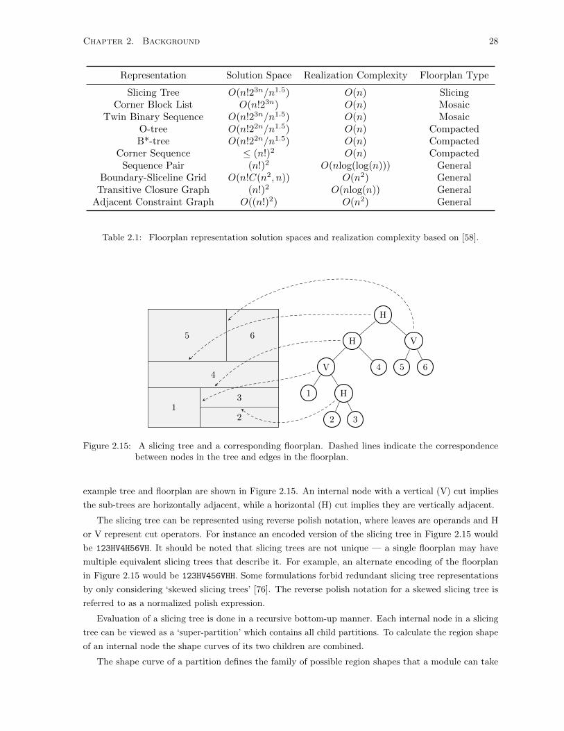
Chapter 2. Background 28
Representation Solution Space Realization Complexity Floorplan Type
Slicing Tree O(n!23n/n1.5) O(n) SlicingCorner Block List O(n!23n) O(n) Mosaic
Twin Binary Sequence O(n!23n/n1.5) O(n) MosaicO-tree O(n!22n/n1.5) O(n) CompactedB*-tree O(n!22n/n1.5) O(n) Compacted
Corner Sequence ≤ (n!)2 O(n) CompactedSequence Pair (n!)2 O(nlog(log(n))) General
Boundary-Sliceline Grid O(n!C(n2, n)) O(n2) GeneralTransitive Closure Graph (n!)2 O(nlog(n)) General
Adjacent Constraint Graph O((n!)2) O(n2) General
Table 2.1: Floorplan representation solution spaces and realization complexity based on [58].
H
V
65
H
4V
H
32
1
12
3
4
5 6
Figure 2.15: A slicing tree and a corresponding floorplan. Dashed lines indicate the correspondencebetween nodes in the tree and edges in the floorplan.
example tree and floorplan are shown in Figure 2.15. An internal node with a vertical (V) cut implies
the sub-trees are horizontally adjacent, while a horizontal (H) cut implies they are vertically adjacent.
The slicing tree can be represented using reverse polish notation, where leaves are operands and H
or V represent cut operators. For instance an encoded version of the slicing tree in Figure 2.15 would
be 123HV4H56VH. It should be noted that slicing trees are not unique — a single floorplan may have
multiple equivalent slicing trees that describe it. For example, an alternate encoding of the floorplan
in Figure 2.15 would be 123HV456VHH. Some formulations forbid redundant slicing tree representations
by only considering ‘skewed slicing trees’ [76]. The reverse polish notation for a skewed slicing tree is
referred to as a normalized polish expression.
Evaluation of a slicing tree is done in a recursive bottom-up manner. Each internal node in a slicing
tree can be viewed as a ‘super-partition’ which contains all child partitions. To calculate the region shape
of an internal node the shape curves of its two children are combined.
The shape curve of a partition defines the family of possible region shapes that a module can take

Chapter 2. Background 29
h
w
h = A/w
(a) An shape curve with unboundedaspect ratio.
h
w
h = γmaxw
h = γminw
(b) An shape curve with bounded as-pect ratio.
h
w
•
••
(c) A piece-wise linear approxima-tion to the shape curve.
h
w
◦◦ ◦
l
◦
◦◦
r
•
••
m
l
r
l
r
(d) A horizontally sliced super-module shape curve(bold) combined from its children shape curves(dotted).
h
w
◦◦
◦
l◦
◦
◦
r•
•
•
m
l r
l r
(e) A vertically sliced super-module shape curve (bold)combined from its children shape curves (dotted).
Figure 2.16: Shape curve example.
on while satisfying its area and aspect ratio constraints. An example shape curve for a partition with
fixed area and unbounded aspect ratio is shown in Figure 2.16a, where the shape curve is defined by the
hyperbola h = A/w. The imposition of aspect ratio constraints shown in Figure 2.16b restricts valid
solutions to only those parts of the hyperbola falling between the two aspect ratio limits.
To determine the region shape of a partition from its two children the two shape curves are combined
either vertically or horizontally by adding their shape curves. A common approach is to approximate the
true shape curve with a piece-wise linear shape curve. Then the super-partition’s region shapes can be
found by combining only the ‘corner points’ of the child shape curves (where the piece-wise curve changes
slope). For a horizontal slice as shown in Figure 2.16d, the two shape curves are combined such that
the height of the super-partition’s region shapes are the sum of the sub-partition’s region heights, and
the widths are the maximum of the sub-partition’s region widths. The vertical combination operation
(Figure 2.16e) is similar, except the maximum of the heights and sum of the widths are used to calculate
the dimensions of the super-partition region shapes. Performing the combination operations from leaves
to the root of the tree generates a final shape curve (family of solutions) at the root, from which the best
point (e.g. minimum area) can be selected.
A slicing tree with N leaves (representing netlist partitions) has 2N − 1 = O(N) nodes. Since each
node in the tree can be combined in O(K) time (assuming a maximum of K corner points) a slicing tree
can be evaluated in O(NK) time.
B*-Trees
B*-trees [70] are another floorplan representation, which encode the class of compacted floorplans
— floorplans where there is no white-space can be removed by shifting modules down or to the left.
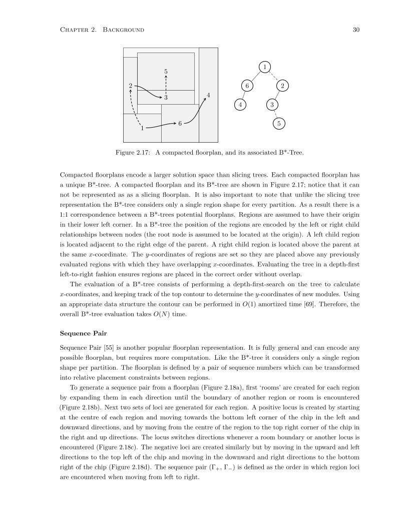
Chapter 2. Background 30
1
2
3
5
6
4
4
16
2
5
3
Figure 2.17: A compacted floorplan, and its associated B*-Tree.
Compacted floorplans encode a larger solution space than slicing trees. Each compacted floorplan has
a unique B*-tree. A compacted floorplan and its B*-tree are shown in Figure 2.17; notice that it can
not be represented as as a slicing floorplan. It is also important to note that unlike the slicing tree
representation the B*-tree considers only a single region shape for every partition. As a result there is a
1:1 correspondence between a B*-trees potential floorplans. Regions are assumed to have their origin
in their lower left corner. In a B*-tree the position of the regions are encoded by the left or right child
relationships between nodes (the root node is assumed to be located at the origin). A left child region
is located adjacent to the right edge of the parent. A right child region is located above the parent at
the same x-coordinate. The y-coordinates of regions are set so they are placed above any previously
evaluated regions with which they have overlapping x-coordinates. Evaluating the tree in a depth-first
left-to-right fashion ensures regions are placed in the correct order without overlap.
The evaluation of a B*-tree consists of performing a depth-first-search on the tree to calculate
x-coordinates, and keeping track of the top contour to determine the y-coordinates of new modules. Using
an appropriate data structure the contour can be performed in O(1) amortized time [69]. Therefore, the
overall B*-tree evaluation takes O(N) time.
Sequence Pair
Sequence Pair [55] is another popular floorplan representation. It is fully general and can encode any
possible floorplan, but requires more computation. Like the B*-tree it considers only a single region
shape per partition. The floorplan is defined by a pair of sequence numbers which can be transformed
into relative placement constraints between regions.
To generate a sequence pair from a floorplan (Figure 2.18a), first ‘rooms’ are created for each region
by expanding them in each direction until the boundary of another region or room is encountered
(Figure 2.18b). Next two sets of loci are generated for each region. A positive locus is created by starting
at the centre of each region and moving towards the bottom left corner of the chip in the left and
downward directions, and by moving from the centre of the region to the top right corner of the chip in
the right and up directions. The locus switches directions whenever a room boundary or another locus is
encountered (Figure 2.18c). The negative loci are created similarly but by moving in the upward and left
directions to the top left of the chip and moving in the downward and right directions to the bottom
right of the chip (Figure 2.18d). The sequence pair (Γ+, Γ−) is defined as the order in which region loci
are encountered when moving from left to right.
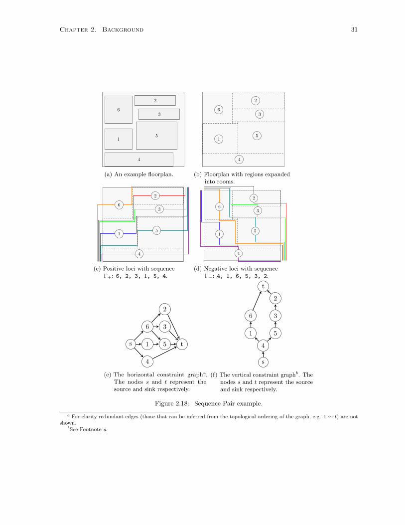
Chapter 2. Background 31
1
2
3
4
5
6
(a) An example floorplan.
1
2
3
4
5
6
(b) Floorplan with regions expandedinto rooms.
1
2
3
4
5
6
(c) Positive loci with sequenceΓ+: 6, 2, 3, 1, 5, 4.
1
2
3
4
5
6
(d) Negative loci with sequenceΓ−: 4, 1, 6, 5, 3, 2.
s 1
4
6
5
3
2
t
(e) The horizontal constraint grapha.The nodes s and t represent thesource and sink respectively.
s
4
1 5
6 3
2
t
(f) The vertical constraint graphb. Thenodes s and t represent the sourceand sink respectively.
Figure 2.18: Sequence Pair example.
a For clarity redundant edges (those that can be inferred from the topological ordering of the graph, e.g. 1 t) are notshown.
bSee Footnote a

Chapter 2. Background 32
From the sequence pair it is then possible to derive the horizontal (Figure 2.18e) and vertical constraint
graphs (Figure 2.18f) which define the relative region positions. If an edge u v exists between regions
u and v in the vertical (horizontal) constraint graph, then it means region u is to the below (left) of
region v.
In the sequence pair representation, a region i is said to be left of region j (i.e. there is an edge i j
in the horizontal constraint graph) if i precedes j in both Γ+ and Γ−. For instance, in the example shown
in Figure 2.18, region 6 is located to the left of region 2, 3 and 5 (Figure 2.18e), since 6 precedes {2, 3,
5} in both Γ+ and Γ−.
Similarly, a region i is said to be below region j (i.e. there is an edge i j in the vertical constraint
graph) if i follows j in Γ+, but i precedes j in Γ−. For example, in Figure 2.18, region 4 is below regions
1 and 5, since 4 follows {1, 5} in Γ+, but 4 precedes {1, 5} in Γ−.
With the two constraint graphs, and assuming fixed region sizes, each module’s x and y coordinates
can be determined by performing a longest path search from the source to each of the N modules. Since
the constraining graphs are DAGs, this search can be performed in O(N) time [77]. As a result the overall
time complexity is O(N2). Further work has developed alternative algorithms with better asymptotic
complexity, taking O(Nlog(N)) [78] or O(Nlog(log(N))) [79] time.
Comments on Floorplan Representations
While extensive research has been conducted into floorplan representations, it is still not clear which
representations are best. In particular, while numerous theoretical properties have been proved about
the representations, such as the size of their solution space, the existence of redundancies in the solution
space, and the complexity of manipulating them, it is not clear what set of properties are desirable.
In [75], Chan et al. compared both the B*-tree and sequence pair representations under a variety of
scenarios including both fixed and non-fixed outline constraints, soft and hard modules, and under both
area and combined area/wirelength optimization objectives. They concluded that the theoretical results
associated with the two floorplan representations had little relevance to real-world optimization efficacy.
They found that the O(N2) sequence pair evaluation algorithm outperformed the other O(Nlog(N) and
O(Nlog(log(N))) algorithms, and the O(N) B*-tree evaluation on realistically sized problems (N < 300).
Properties such as containing redundant solutions or excluding area optimal floorplans had no significant
impact. Furthermore, they found that overall run-time was dominated by other factors unrelated to the
choice of representation such as wirelength evaluation, and that both run-time and solution quality were
largely controlled by the annealing schedule.
2.8 Floorplanning for FPGAs
In an ASIC there is only a single type of resource, silicon area, which can be used to implement any type
of netlist primitive In contrast, as described in Section 2.1.1, modern FPGAs are highly heterogeneous,
possessing multiple different types of resources. This makes the FPGA floorplanning problem a case of
the heterogeneous floorplanning problem (Equation (2.6)). However there is another important difference
between the ASIC and FPGA floorplanning problems. The prefabricated nature of FPGAs means that
resources are available only in discrete increments and can not (unlike the silicon area in ASICs) be
allocated at an arbitrary level of granularity.
Chapter 2. Background 33
These restrictions mean that several key properties typically assumed by ASIC floorplanners do not
hold for FPGA floorplanning:
Regions are not translationally or rotationally invariant
Unlike on an ASIC, on an FPGA a region can not be translated to another location (or rotated)
and be assumed legal. Only specific locations on the FPGA device may have the correct type or
quantity of resources.
Region shapes and positions are not continuous variables
The prefabricated resources force region dimensions, and positions to take on only a discrete set of
values, making it a discrete (combinatorial) optimization problem.
This means that many techniques used for ASIC floorplanning either do not apply or require significant
modification to be applied to FPGAs. For instance, the analytic floorplanner in [61] (Section 2.7.1)
shifts modules horizontally and vertically and resizes them during the floorplanning process to reduce
overlap. Neither technique can be directly applied to FPGA floorplanning as each requires modules to be
translationally invariant. Additionally the conjugate gradient method can only be used with continuous
variables. As another example, consider that B*-trees (Section 2.7.3) can only represent compacted
floorplans. In an ASIC compaction involves translating modules as far to the lower-left as possible; this
transformation may result in an invalid floorplan on an FPGA.
2.8.1 FPGA Floorplanning Techniques
While some early approaches address floorplanning for FPGAs, they make assumptions about the device
architecture that are not valid on modern FPGAs. For instance they target uniform (non-heterogeneous)
FPGAs [80, 81], or hierarchical FPGA architectures [82] which are no longer popular commercially.
Simulated Annealing Floorplanning
The first to address the heterogeneous floorplanning problem were Cheng and Wong [56]. They created a
SA floorplanner based around the slicing tree representation. Their key contribution was the development
of Irreducible Realization Lists (IRLs), which enable the creation of legal FPGA floorplans from a slicing
tree. An IRL is defined as a set of irreducible shapes (i.e. the smallest at each aspect ratio) that
can legally implement a netlist module when rooted at a specific location on the FPGA (Figure 2.19).
Although not presented as such in [56], IRLs serve a similar purpose as the shape curves used in ASIC
floorplanning — both describe a family of possible region shapes for a logical netlist partition. The key
differences (some shown in Figure 2.20) between shape curves and IRLs are:
1. IRLs are not continuous. Instead of being assumed piece-wise linear, an IRL consists of a discrete
set of points (each a potential region shape).
2. The potential region shapes in an IRL do not necessarily have the same area — they do not appear
along the constant area parabola A = wh. Since area is no longer the resource being allocated it
becomes a free variable, determined by the region dimensions required to satisfy the associated
partition’s resource requirements.
3. IRLs are specified not only by the partition they represent, but also by a location. Since translational
invariance does not hold, IRLs at different locations do not (necessarily) describe the same sets of
region shapes.

Chapter 2. Background 34
0 1 2 3 4 5 6 7 8 9x
0
1
2
3
4
5
6
7
8
9
y
LB
RA
M
DS
P
A (2, 9)
B (3, 5)
D (10, 2)
C (6, 3)
E: (4,5)
F:(5,4)
Figure 2.19: Example IRLs for resource vector φ = (nlb, nram, ndsp) = (9, 2, 0). The IRL rooted at (0, 0)consists of four rectangles: A, B, C, and D. The IRL rooted at (5, 4) consists of 2 rectangles:E, and F. Rectangle dimensions (width, height) are annotated on the figure.
h
w
•
••
(a) An ASIC-style piece-wise linearshape curve, valid for every (x, y)location.
h
w
•
• •◦
◦
◦◦
(b) IRLs for a module at two uniquelocations, shown as ‘•’ and ‘◦’respectively.
Figure 2.20: Shape curve and IRL comparison.

Chapter 2. Background 35
The discrete nature of IRLs means they can not be added together like shape curves. However the
recursive structure of the slicing tree can still be used to calculate an IRL for the root node in a bottom-up
fashion. To do this we need to be able to calculate IRLs for internal nodes (super-partitions) in the
slicing tree. The naive approach is shown in Algorithm 2.
Given a location and slicing tree node we recursively calculate the IRL associated with the left child
node (line 4). Then for every shape in the left child IRL we determine the location of the right child node
(lines 7-12) and recursively calculate the IRL associated with it (line 13). The shapes from the left and
right IRL are then combined and added to a new IRL if they are not redundant (lines 15-22). Finally the
new IRL representing the super-partition is returned. For the base case of the recursive calculation the
IRLs of leaf nodes are calculated directly by Algorithm 3, which enumerates all possible shapes.
Algorithm 2 Naive IRL Slicing Tree Evaluation
Require: S a slicing tree node, xleft and yleft the coordinates of the IRL1: function NaiveCalculateIRL(S, xleft, yleft)2: if S is a leaf then . Recursion base case3: return NaiveLeafIRL(S, xleft, yleft)
4: IRLleft ← NaiveCalculateIRL(S.left, xleft, yleft) . Recursively calc. left child IRL5: IRLnew ← ∅6: for each Shapeleft ∈ IRLleft do7: if S is vertically sliced then . Determine coordinates of right child IRL8: xright ← xleft + Shapeleft.width9: yright ← yleft
10: else if S is horizontally sliced then11: xright ← xleft12: yright ← yleft + Shapeleft.height
13: IRLright ← NaiveCalculateIRL(S.right, xright, yright) . Recursively calc. right child IRL14: for each Shaperight ∈ IRLright do15: if S is vertically sliced then . Combine region shapes16: Shapenew.width← Shapeleft.width+ Shaperight.width17: Shapenew.height← max(Shapeleft.height, Shaperight.height)18: else if S is horizontally sliced then19: Shapenew.width← max(Shapeleft.width, Shaperight.width)20: Shapenew.height← Shapeleft.height+ Shaperight.height
21: if Shapenew not redundant in IRLnew then22: add Shapenew to IRLnew23: return IRLnew
The complexity of the naive approach is quite high. To alleviate this Cheng and Wong presented
several techniques to make the algorithm more efficient. First, they recognized that the IRLs of leaf
nodes are calculated multiple times. This redundant work can be eliminated by pre-calculating the leaf
IRLs once and re-using the results. Secondly, since Algorithm 2 enumerates all combinations of shapes in
the left and right child IRLs it generates numerous redundant shapes. Cheng and Wong showed that
the bounds on the loops at lines 6 and 14 can be tightened, so that only a subset of shapes need to be
combined to generate the IRL of the super-module.
Another optimization made by Cheng and Wong was to assume that the targeted FPGA followed a
repeating ‘basic pattern’ (also referred to as a ‘basic tile’ by other authors), with width wp and height
hp. Figure 2.21 illustrates the basic pattern of a simple heterogeneous FPGA. The basic pattern can

Chapter 2. Background 36
Algorithm 3 Naive Leaf IRL Evaluation
Require: S a slicing tree leaf node, x and y the coordinates of the IRL1: function NaiveLeafIRL(S, x, y)2: IRLleaf ← ∅3: for each w ∈ 1 . . .W do4: for each h ∈ 1 . . . H do5: Shapeleaf .width← w . Consider all shapes up to (Wmax, Hmax)6: Shapeleaf .height← h7: if Shapeleaf not redundant in IRLleaf then8: if Shapeleaf satisfies resource requirements of S then9: add Shapeleaf to IRLleaf
10: return IRLleaf
wp = 6
hp = 6
Figure 2.21: The basic 6× 6 pattern of a pattern-able FPGA.
be viewed as a weak form of translational invariance, since (assuming an infinite size FPGA) different
locations mapping to the same location on the basic pattern would be indistinguishable. This can be
exploited to reduce the computational complexity by only calculating IRLs only for each unique location
on the basic pattern.
The overall complexity of Cheng and Wong’s optimized IRL calculation approach is reported as
O(Nlwphplog(l)), where N is the number of partitions, wp and hp are the dimensions of the basic pattern
and l is the maximum of the device width or height.
While Algorithm 2 (or Cheng and Wong optimized version) allows us to calculate an IRL for a slicing
tree rooted at a specific (x, y) location it is not immediately clear what location (or locations) should
be chosen. Cheng and Wong showed that it suffices to only calculate the slicing IRL at the origin of
the FPGA device (i.e. the lower left corner). This means that given a slicing tree only a single call to
NaiveCalculateIRL(Sroot, 0, 0) is required to evaluate it.
Cheng and Wong also implement a post processing step that vertically compacts the modules in the
floorplan. This allows them to generate rectilinear (rather than just rectangular) shapes, allowing them
Chapter 2. Background 37
to find more legal solutions and reduce overall run time, since it speeds-up the annealing process.
To generate an initial solution, a conventional area driven floorplanner is used, which helps to reduce
run time (traditional floorplanning is much quicker) and yields a better initial solution allowing the
heterogeneous floorplanner to start at a lower temperature. The heterogeneous floorplanner cost function
includes terms for area, external wirelength and internal wirelength (approximated by module aspect
ratios).
Network Flow Floorplanning
In [83] Feng and Mehta presented another approach to heterogeneous FPGA floorplanning. They use a
conventional floorplanner to create an initial rough floorplan, and then legalize it by formulating and
solving a network flow problem.
Feng and Mehta used Parquet [84], an ASIC floorplanner, to perform initial floorplanning. They
adapt parquet to consider heterogeneity by adding a resource mismatch penalty to the cost function,
which aims to ensure that the initial floorplan is fairly close to being legal.
Given the initial floorplan, it is expanded by one LB unit in each direction to convert from Parquet’s
floating-point coordinate system to the integer coordinate system of the FPGA. Since the floorplan regions
likely do not satisfy their module resource requirements, the authors formulate a max-flow problem to
assign resources to each region. This allows them have a global view during resource allocation. Their
algorithm does not guarantee that a module’s resources will be in a contiguous region (e.g. RAM and LBs
may be at different locations). To try and avoid this they use a min-cost max-flow algorithm which allows
them to place costs on edges in the flow graph which are used to pull disconnected regions together.
They report their resource allocation algorithm as requiring O(N2blockslog(Nblocks)) time, where Nblocks
is the number of resources on the FPGA (not the number of partitions).
Greedy Floorplanning
Yuan et al. [85] present a greedy algorithm (with optional backtracking-like behaviour) for heterogeneous
FPGA floorplanning. The guiding principle behind their algorithm is to pack modules with the ‘Least
Flexibility First’; that is they leave the most flexible modules to be placed last. They identify several
different types of flexibility including location flexibility (whether a module is being placed at a corner,
edge or not adjacent to anything else), how many resources it requires, how large its realizations are and
how tightly interconnected a module is to those around it.
They first calculate the realizations for each module based on the current partial floorplan and rank
them by their flexibilities. Next they select the least flexible module which is placed into the current
partial floorplan. The remaining modules are then greedily placed into the floorplan if possible. From the
resulting floorplan they calculate a fitness value for the initial placed module and revert both the initial
and the greedily placed modules (this is similar to backtracking). By repeating this process for all module
realizations they can determine the ‘fittest’ module realization which is then permanently placed into the
floorplan. The process continues until all modules have been truly packed or no solution is found. The
authors report their algorithm as having a high asymptotic complexity, O(W 2N5log(N)) where W is the
width of the device and N is the number of modules, but that it achieves a lower complexity in practice.

Chapter 2. Background 38
Multi-Layer Floorplanning
In [86] and [87], Singhal and Bozorgzadeh develop a multi-layered approach to heterogeneous floorplanning.
The key insight of their approach is that using a single rectangular region for all resource types can lead
to poor resource utilization. For example, a module which requires a large amount of a relatively rare
resource such as DSP blocks may end up with an excess amount of another resource type (such as LBs).
They propose to allow each resource type a separate rectangular region, essentially placing each resource
type in its own layer.
Their floorplanner is based on the ASIC floorplanner Parquet [84] and uses the sequence pair
representation. They extended the interpretation of the horizontal and vertical constraints so that they
apply to all rectangular regions across all layers (i.e. for a given module the regions in each layer have
the same relative location across all layers).
The above formulation does not guarantee that the multiple regions for a partition will overlap in
the final floorplan. The authors attempt to maximize this overlap while packing the sequence pair in
topological order. Instead of performing the traditional area minimization on each layer, they identify
the critical layer and attempt to shift the regions for other resources towards the center-point of the
critical layer.
Partitioning Based Floorplanning
Banerjee et al. present a deterministic heterogeneous FPGA floorplanner [88]. Their floorplanner has
three distinct phases. The first phase uses hMetis [89] to recursively divide (bi-partition) the input netlist
into multiple parts. The second phase generates slicing floorplan topologies based on the partition tree
created by hMetis. The third phase uses a combination of greedy heuristics and max-flow to generate
realizations of the slicing floorplan topologies.
In the first phase, modules are generated from the input netlist using the hMetis partitioning tool.
The weight (number of elements) in each partition is balanced during partitioning to produce modules of
similar size. The authors note that the generated partitioning tree provides a good guide for generating
potential floorplan topologies, in particular because it keeps tightly connected modules close together in
the final partitioning.
In the second phase, potential module shapes and slicing trees (topologies) are generated. For each
module a list of irredundant shapes is created. Each of these shapes is defined in terms of the width and
height of the FPGA architecture’s basic pattern that satisfy the modules resource requirements. This is
broadly similar to the IRLs described in [56], however realizations are built out of sets of entire basic
patterns, instead of precisely sized regions that may contain only fractions of basic patterns. To generate
a set of slicing trees, sub-floorplans are constructed for all of the internal nodes of the partition tree
generated by hMetis in the first phase. This is done in a similar recursive bottom-up manner as in [56],
but considers both horizontal and vertical cuts at each internal node to generate a wider set of floorplan
topologies. The list of slicing trees eventually generated at the root of the partitioning tree corresponds
to the floorplan topologies being considered.
The third phase produces realizations of the slicing trees generated in phase two. To allocate space
for LBs, the authors use a greedy technique. Initially allocating the whole chip to the root node of the
slicing tree, the region is divided by a cut line (either horizontal or vertical depending on the slicing tree)
based on the number of LBs required by the left and right children (sub-floorplans). This process then
Chapter 2. Background 39
continues level by level until the leaf nodes are reached. The top-down greedy LB allocation ensures that
each module has enough LBs, but does not guarantee that the allocated region has sufficient non-LB
resources like RAM or DSP blocks. To ensure that sufficient resources are allocated, the authors resize a
module’s allocated region by expanding it vertically along the columns of RAM and DSP blocks. Since
there may be conflicting requirements between adjacent modules, the authors formulate a network-flow
problem along each column. This allows for global optimization along each column of RAM/DSP blocks.
If no feasible solution can be found the slicing tree is marked as infeasible. If none of the slicing trees
generated in phase two are feasible, hMetis (phase one) must be re-run with a new module ordering to
create a new partitioning tree. Feasible floorplans generated by phase three are then ranked based upon
their wirelength and reported to the user.
The authors report that their algorithm (excluding hMetis) takes O(lN3 + lN2H2log2(H)), where N
is the number of modules, l is the maximum of device width or height, and H is the height of the targeted
FPGA. The authors extended their floorplanning technique to handle partial reconfiguration in [90].
2.8.2 Comments on FPGA Floorplanning Techniques
The simulated annealing approach presented by Cheng and Wong introduced many important concepts
for FPGA floorplanning including IRLs and resource vectors. These have formed the basis for much of
the following work. While their IRL combination and compaction algorithms are effective at finding
legal FPGA floorplans, they are computationally expensive operations to be used in the inner loop of an
annealer. One of the issues with this work (and many of the other works on FPGA floorplanning) is that
they do not use realistic benchmarks to evaluate their floorplanners, instead relying on adapted ASIC
floorplanning benchmarks with arbitrarily added heterogeneous resources.
The network flow approach presented by Feng and Mehta is an interesting technique, however the
quadratic runtime dependence on the device size limits its scalability, since device sizes double every 2-3
years. It is also unclear how well this technique would fare on more realistic benchmarks with unequal
heterogeneous resource distributions between modules. This would likely make the initial floorplan
produced by Parquet significantly less useful, hurting quality and runtime.
Yuan et al.’s greedy floorplanning algorithm makes some insightful observations about the floorplanning
problem, but its high complexity is problematic. Furthermore, only a limited evaluation is presented
using synthetic benchmarks, making it unclear how it compares to other approaches.
The multi-layer floorplanning approach presented by Singhal and Bozorgzadeh is the only work
evaluated in the context of unbalanced heterogeneous resources. They show that the multi-layer approach
is more area efficient than a conventional (single-layer) floorplanner. However the use of synthetic
benchmarks and limited empirical evaluation makes it unclear how robust this approach is, and what
impact it has on quality (e.g. wirelength).
As noted Banerjee et al.’s approach is similar to Cheng and Wong’s, but uses a different technique
to generate slicing trees, and allocates resources on a coarser granularity. While this approach is faster
empirically, it finds a small number of solutions for the benchmarks evaluated. It is therefore unclear
how effective this technique would be on more difficult problems using more realistic benchmarks.
Chapter 3
Titan: Large Benchmarks for FPGA
Architecture and CAD Evaluation
If you can not measure it, you can not improve it.
— Lord Kelvin
3.1 Motivation
Most research into FPGA architecture and CAD is based on empirical methods. A given set of benchmark
circuits are mapped to an FPGA architecture using CAD tools and the results evaluated to identify the
strengths and weaknesses of the architecture and CAD tools. This empirical approach makes research
conclusions dependant upon the methodology used [91], since the impact of each of these three components
(architecture, CAD, and benchmarks) can not be completely isolated from the others.
While FPGA architecture and CAD tools have been heavily researched in academia some of the
benchmarks commonly used to evaluate them, such as the MCNC benchmarks [26], are nearly 25 years
old. Given the rapid growth in device size and complexity associated with Moore’s Law, this means that
these benchmarks are significantly (∼ 100×) smaller than modern devices. More recent benchmark sets,
such as the VTR benchmarks [25] improve upon this, but there still remains a large gap between the
benchmarks used in academic research and the size and capabilities of modern FPGA devices.
In-order to trust academic research conclusions it is therefore important to:
1. Identify and address the barriers that have prevented improved benchmark suites from being created
and used, and
2. Develop a modern, large-scale and realistic set of benchmarks suitable for evaluating FPGA
architectures and CAD tools.
3.2 Introduction
There are many barriers to the use of state-of-the-art benchmark circuits with open-source academic
tool flows. First, obtaining large benchmarks can be difficult, as many are proprietary. Second, purely
open-source flows have limited HDL coverage. The VTR flow [25], for example, uses the ODIN-II Verilog
40
Chapter 3. Titan: Large Benchmarks for FPGA Architecture and CAD Evaluation 41
parser which can process only a subset of the Verilog HDL — any design containing System Verilog,
VHDL or a range of unsupported Verilog constructs cannot be used without a substantial re-write. As
well, if part of a design was created with a higher-level synthesis tool, the output HDL is not only likely
to contain constructs unsupported by ODIN-II, but is also likely to be difficult to read and re-write using
only supported constructs. Third, modern designs make extensive use of IP cores, ranging from low-level
functions such as floating-point multiply and accumulate units to higher-level functions like FFT cores
and off-chip memory controllers. Since current open-source flows lack IP, all these functions must be
removed or rewritten; this is not only a large effort, it also raises the question of whether the modified
benchmark still accurately represents the original design, as IP cores are often a large portion of the
design logic.
In order to avoid many of these pitfalls, we have created Titan, a hybrid CAD flow that utilizes a
commercial tool, Altera’s Quartus II design software, for HDL elaboration and synthesis, followed by a
format conversion tool to translate the results into conventional open-source formats. The Titan flow has
excellent language coverage, and can use any unencrypted IP that works in Altera’s commercial CAD
flow, making it much easier to handle large and complex benchmarks. We output the design early in the
Quartus II flow, which means we can change the target FPGA architecture and use open-source synthesis,
placement and routing engines to complete the design implementation. Consequently we believe we have
achieved a good balance between enabling realistic designs, while still permitting a high degree of CAD
and architecture experimentation.
We have also provided a high-quality architecture capture of Altera’s Stratix IV architecture including
support for carry chains, direct-links between adjacent blocks, and a detailed timing model. This
enables timing-driven CAD and architecture research and a detailed comparison of academic and Altera’s
commercial CAD tools.
Contributions include:
• Titan, a hybrid CAD flow that enables the use of larger and more complex benchmarks with
academic CAD tools.
• The Titan23 benchmark suite. This suite of 23 designs has an average size of 421,000 primitives.
Most designs are highly heterogeneous with thousands of RAM and/or multiplier primitives.
• A timing driven comparison of the quality and run time of the academic VPR and the commercial
Quartus II packing, placement and routing engines. This comparison helps identify how academic
tool quality compares to commercial tools, and highlights several areas for potential improvement
in VPR.
3.3 The Titan Flow
The basic steps of the Titan flow are shown in Figure 3.1. Quartus II performs elaboration and synthesis
(quartus map) generating a Verilog Quartus Map (VQM) file. The VQM file is a technology mapped
netlist, consisting of the basic primitives in the target architecture; see Table 3.3 for primitives in the
Stratix IV architecture. The VQM file is then converted to the standard Berkeley Logic Interchange
Format (BLIF), which can be passed on to conventional open-source tools such as ABC [92] and VPR
[93].
The conversion from VQM to BLIF is performed using our VQM2BLIF tool. At a high level, this tool
performs a one-to-one mapping between VQM primitives and BLIF .subckt, .names, and .latch structures.

Chapter 3. Titan: Large Benchmarks for FPGA Architecture and CAD Evaluation 42
ARCH
quartus_map
HDL
VQM2BLIF
VPR ABC
VQM
BLIF
Figure 3.1: The Titan Flow.
To convert a VQM primitive to BLIF, the VQM2BLIF tool requires a description of the primitive’s input
and output pins. VPR also requires this information to parse the resulting BLIF; we store it in the VTR
architecture file for use by both tools.
VQM2BLIF can output different BLIF netlists to match a variety of use cases. Circuit primitives
such as arithmetic, multipliers, RAM, Flip-Flops, and LUTs are usually modelled using BLIF’s .subckt
structure, which represents these primitives as black boxes. While this is usually sufficient for physical
design tools like VPR, some primitives like LUTs and Flip-Flops can also be converted to the standard
BLIF .names and .latch primitives respectively. This allows the circuit functionality to be understood by
logic synthesis tools such as ABC. VQM2BLIF also supports more detailed conversions of VQM primitives,
depending on their operation mode. This allows downstream tools, for instance, to differentiate between
RAM blocks operating in single or dual port modes.
Some benchmarks make use of bidirectional pins, which cannot be modelled in BLIF. Therefore
VQM2BLIF splits any bidirectional pins into separate input and output pins, and makes the appropriate
changes to netlist connectivity. While Quartus II will recognize that netlist primitive ports connected to
vcc or gnd can be tied off within the primitive, VPR does not and will attempt to route these (potentially
high fan-out) constant nets. To avoid this behaviour the VQM2BLIF netlist converter removes such
constant nets from the generated BLIF netlist.
It is also important to note that the sizes of benchmarks created with the Titan flow are not limited
by the capacity of the targeted FPGA family. Quartus II’s synthesis engine does not check whether the
design will fit onto the target device, allowing VQM files to be generated for designs larger than any
current commercial FPGA. The VQM2BLIF tool also runs quickly, taking less than 4 minutes to convert
our largest benchmark.
The VQM2BLIF tool, detailed documentation, scripts to run the Titan flow, along with the complete
benchmark set and Stratix IV architecture capture, are available from: http://www.eecg.toronto.edu/
~vaughn/software.html.

Chapter 3. Titan: Large Benchmarks for FPGA Architecture and CAD Evaluation 43
3.4 Flow Comparison
Using a commercial tool like Quartus II as a “front-end” brings several advantages that are hard to
replicate in open-source flows. It supports several HDLs including Verilog, VHDL and SystemVerilog, and
also supports higher level synthesis tools like Altera’s QSYS, SOPC Builder, DSP Builder and OpenCL
compiler. It also brings support for Altera’s IP catalogue, with the exception of some encrypted IP
blocks.
These factors significantly ease the process of creating large benchmark circuits for open-source CAD
tools. For example, converting an LU factorization benchmark [12] for use in the VTR flow [25] involved
roughly one month of work removing vendor IP and re-coding the floating point units to account for
limited Verilog language support. Using the Titan flow, this task was completed in less than a day, as it
only required the removal of one encrypted IP block from the original HDL, which accounted for less
than 1% of the design logic. In addition, since over 68% of the design logic was in the floating point units,
the Titan flow better preserves the original design characteristics.
Experiment Modification VTR Titan Titan Flow Method
Device Floorplan Yes Yes Architecture fileInter-cluster Routing Yes Yes Architecture fileClustered Block Size / Configuration Yes Yes Architecture fileIntra-cluster Routing Yes Yes Architecture fileLogic Element Structure Yes Yes Architecture fileLUT size / Combinational Logic Yes Yes ABC re-synthesisNew RAM Block Yes Yes Architecture file (up to 16K depth)New DSP Block Yes Yes Architecture file (up to 36 bit width)New Primitive Type Yes No No method to synthesize new primitives with Quartus II
Table 3.1: Comparison of architecture experiments supported by the VTR and Titan flows.
A concern in using a commercial tool to perform elaboration and synthesis is that the results may be
too device or vendor-specific to allow architecture experimentation. However this is not necessarily the
case. The Titan flow still allows a wide range of experiments to be conducted as shown in Table 3.1. The
ability to use tools like ABC to re-synthesize the netlist ensures experiments with different LUT sizes,
and even totally different logic structures such as AICs [94], can still occur. RAM is represented as device
independent “RAM slices” which are typically one bit wide, and up to 14 address bits deep. These RAM
slices are packed into larger physical RAM blocks by VPR, and hence arbitrary RAM architectures can
be investigated. Similarly, multiplier primitives (up to 36× 36 bits) are packed into DSP blocks by VPR,
allowing a variety of experiments. A simple remapping tool could also re-size the multiplier primitives if
desired. The structure of a logic element (connectivity, number of Flip-Flops, etc.) can also be modified
without having to re-synthesize the design, and inter-block routing architecture and electrical design can
both be arbitrarily modified. Compared to VTR, the largest limitation is the inability to add support for
new primitive types, such as a floating point block [25]. It may be possible to force Quartus II to output
a new primitive in the future by placing an empty ‘blackbox’ module in the input HDL, but this has not
been investigated.
Another use of Titan is to test and evaluate CAD tool quality. Both physical CAD (e.g. packing,
placement, routing) and logic re-synthesis tools can be plugged into the flow. Titan provides a front-end
interface between commercial and academic CAD flows which is complementary to the back-end VPR to
bitstream interface presented in [95]. Overall, the Titan flow enables a wide range of FPGA architecture
experiments, and can be used to evaluate new CAD algorithms on realistic architectures with realistic

Chapter 3. Titan: Large Benchmarks for FPGA Architecture and CAD Evaluation 44
benchmark circuits, and allows for more extensive scalability testing with larger benchmarks.
3.5 Benchmark Suite
We selected the 23 largest benchmarks that we could obtain from a diverse set of application domains
to create the Titan23 benchmark suite. The benchmarks often required minor alteration to make them
compatible with the Titan flow.
Name Total Blocks Clocks ALUTs REGs DSP 18x18s RAM Slices RAM Bits Application
gaussianblur 1,859,485 1 805,063 1,054,068 16 334 1,702 Image Processingbitcoin miner 1,061,829 2 455,263 546,597 0 59,968 297,664 SHA Hashing
directrf 934,490 2 471,202 447,032 960 40,029 20,307,968 Communications/DSPsparcT1 chip2 824,152 2 377,734 430,976 24 14,355 1,585,435 Multi-core µPLU Network 630,103 2 194,511 399,562 896 41,623 9,388,992 Matrix Decomposition
LU230 567,992 2 208,996 293,177 924 64,664 10,112,704 Matrix Decompositionmes noc 549,045 9 274,321 248,988 0 25,728 399,872 On Chip Network
gsm switch 491,846 4 159,388 296,681 0 35,776 6,254,592 Communication Switchdenoise 342,899 1 322,021 8,811 192 11,827 1,135,775 Image Processing
sparcT2 core 288,005 2 169,498 109,624 0 8,883 371,917 µP Corecholesky bdti 256,072 1 76,792 173,385 1,043 4,920 4,280,448 Matrix Decomposition
minres 252,454 2 107,971 126,105 614 17,608 8,933,267 Control Systemsstap qrd 237,197 1 72,263 161,822 579 9,474 2,548,957 Radar ProcessingopenCV 212,615 1 108,093 86,460 740 16,993 9,412,305 Computer Vision
dart 202,368 1 103,798 87,386 0 11,184 955,072 On Chip Network Simulatorbitonic mesh 191,664 1 109,633 49,570 676 31,616 1,078,272 Sortingsegmentation 167,917 1 155,568 6,561 104 5,658 3,166,997 Computer VisionSLAM spheric 125,194 1 112,758 8,999 296 3,067 9,365 Control Systems
des90 109,811 1 62,871 30,244 352 16,256 560,640 Multi µP systemcholesky mc 108,236 1 29,261 74,051 452 5,123 4,444,096 Matrix Decompositionstereo vision 92,662 3 38,829 49,049 152 4,287 203,777 Image ProcessingsparcT1 core 91,268 2 41,968 45,013 8 4,277 337,451 µP Core
neuron 90,778 1 24,759 61,477 565 3,799 638,825 Neural Network
Table 3.2: Titan23 Benchmark Suite.
3.5.1 Titan23 Benchmark Suite
The Titan23 benchmark suite consists of 23 designs ranging in size from 90K-1.8M primitives, with the
smallest utilizing 40% of a Stratix IV EP4SGX180 device, and the largest designs unable to fit on the
largest Stratix IV device. The designs represent a wide range of real world applications and are listed in
Table 3.2. All benchmarks make use of some or all of the different heterogeneous blocks available on
modern FPGAs, such as DSP and RAM blocks.
While these benchmarks (as released) will synthesize with Altera’s Quartus II, it should also be
possible to use them in other tool flows such as Torc [96] and RapidSmith [97] by replacing the Altera IP
cores with equivalents from the appropriate vendor.
3.5.2 Benchmark Conversion Methodology
To convert a benchmark from HDL to BLIF, the design was first synthesized in Quartus II. For most
designs this required no HDL modification, but some required replacing vendor/technology specific IP
(e.g. PLLs, explicitly instantiated RAM blocks) with an equivalent Altera implementation, or working
around obscure language features. Once the design was synthesized successfully, the resulting VQM file
could be passed to VQM2BLIF.

Chapter 3. Titan: Large Benchmarks for FPGA Architecture and CAD Evaluation 45
In some cases, benchmark designs required more I/Os than were available on actual Stratix IV devices,
preventing the designs from fitting in Quartus II. In these scenarios, some I/Os were replaced by shift
registers whose input/output was connected to a device pin. This resolves the high I/O demand while
ensuring connected logic can not be optimized away by the logic synthesis tool. This is similar to the
methodology described in [98].
Some IP blocks, such as older DDR memory controllers and the sld mux in some of Altera’s JTAG
controllers are encrypted. These IP blocks were removed from the original HDL to avoid generating an
encrypted VQM file. If possible, an equivalent unencrypted IP block was substituted; this was the case
for some DDR controllers, since new Altera DDR controllers are not encrypted. Once encrypted IP was
removed in the HDL, the design was re-synthesized and the new VQM file passed to VQM2BLIF. In
general, only a small portion of the design logic had to be modified or removed.
3.5.3 Comparison to Other Benchmark Suites
The characteristics outlined above make the Titan23 benchmark suite quite different from the popular
MCNC20 benchmarks [26], which consist of primarily combinational circuits and make no use of
heterogeneous blocks. Furthermore, the MCNC designs are extremely small. The largest (clma) uses
less than 4% of a Stratix IV EP4SGX180 device, making it one to two orders of magnitude smaller than
modern FPGAs. The Titan23 benchmarks are on average 215× larger than the MCNC20 benchmarks.
Another benchmark suite of interest is the collection of 19 benchmarks included with the VTR design
flow. These benchmarks are larger than the MCNC benchmarks, with the largest (mcml) reported to use
99.7K 6-LUTs [25]. Interestingly, when this circuit was run through the Titan flow, it uses only 11.7K
Stratix IV ALUTs (6-LUTs) after synthesis, highlighting the differences between ODINII+ABC and
Quartus II’s integrated synthesis. Additionally, only 10 of the VTR circuits make use of heterogeneous
resources. The Titan23 benchmark suite provides substantially larger benchmark circuits (on average
44× larger than the VTR benchmarks) that also make more extensive use of heterogeneous resources.
Several non-FPGA-specific benchmark suites also exist. The various ISPD benchmarks [99] are
commonly used to evaluate ASIC tools, but are only available in gate-level netlist formats. This makes
them unsuitable for use as FPGA benchmarks, since they are not mapped to the appropriate FPGA
primitives. The IWLS 2005 benchmarks [100] are available in HDL format, and the Titan flow enables
them to be used with FPGA CAD tools. However, the largest design consists of only 36K primitives
after running through the Titan flow — too small to be included in the Titan23.
3.6 Stratix IV Architecture Capture
Recall that to use the Titan flow (without re-synthesis), the architecture file must use the VQM primitives
as its fundamental building blocks. The architecture file can describe an FPGA built out of these
primitives, which can be combined into arbitrary complex blocks with arbitrary routing. We chose to
align our architecture closely with Stratix IV. This allows us to compare computational requirements
and result quality between VPR and Quartus II, and identify possible areas for improvement.
To enable this comparison, a detailed VPR-compatible FPGA architecture description was created
for Altera’s Stratix IV family of 40 nm FPGAs [101]. The Stratix IV device family was selected over
the larger, more recent Stratix V family because of the architecture documentation available as part of

Chapter 3. Titan: Large Benchmarks for FPGA Architecture and CAD Evaluation 46
Altera’s QUIP [102]. As detailed below, this process also identified some limitations in VPR’s architecture
modelling capabilities. Some of the modelled Stratix IV primitives are shown in Table 3.3.
Netlist Primitive Description Model Quality
lcell comb LUT and adder Gooddffeas Register Goodmlab cell LAB LUTRAM Goodmac mult Multiplier Goodmac out Accumulator Goodram block RAM slice Goodio {i,o}buf I/O Buffer Moderateddio {in,out} DDR I/O Moderatepll Phase Locked Loop Poor
Table 3.3: Important Stratix IV primitives.
3.6.1 Floorplan
Stratix IV is an island style FPGA architecture, where the core of the chip is divided into rows and
columns of blocks, and each column is built from a single type of block (LAB, DSP, etc.). The device
aspect ratio and average spacing between blocks were chosen to be typical of devices in the Stratix IV
family. An example floorplan is shown in Figure 3.2.
3.6.2 Global (Inter-Block) Routing
The global or inter-block routing in Stratix IV uses wires 4 and 20 LABs long in the horizontal routing
channels, and wires 4 and 12 LABs long in the vertical routing channels. There are approximately 70%
more horizontal wires than vertical wires. In Stratix IV the long wires are only accessible from the short
wires and not from block pins. Additionally, Stratix IV allows LABs in adjacent columns to directly
drive each other’s inputs.
While VPR can model a mixture of long and short wires, it assumes the same configuration in both
the horizontal and vertical routing channels. Additionally, VPR cannot model Stratix IV’s short to long
wire connectivity. As a result, the inter-block routing was modelled as length 4 and 16 wires (the average
lengths), with both long and short wires accessible from logic block output pins. Unidirectional routing
was used and the channel width (W ) was set to 300 wires, which is close to the 312 wires found in Stratix
IV’s horizontal channels.
3.6.3 Logic Array Block (LAB)
In Stratix IV, each LAB consists of 10 Adaptive Logic Modules (ALMs) with 52 inputs from the global
routing, and 20 feedback connections from the ALM outputs. Stratix IV uses a half-populated crossbar
at the ALM inputs to select from the 72 possible input signals [103, 104]. The LAB has 40 outputs to
global routing driven directly by the ALMs.
Since no detailed information is available on the exact switch patterns used for the half-populated
ALM input crossbars, it was initially modelled as shown in Figure 3.3. However at the time VPR’s packer
performed very poorly on depopulated crossbars, so this was replaced with a full crossbar. Additionally,
while the eight control inputs to the LAB from global routing (clkena, reset, etc.) are also modelled,
their flexibility within the LAB is not. Instead, the eight signals are left fully accessible from each ALM.

Chapter 3. Titan: Large Benchmarks for FPGA Architecture and CAD Evaluation 47
LAB LAB LAB LABLAB
PLL M9K DSP M9K M144K
Figure 3.2: Final placement of the leon2 benchmark using the captured architecture. Column blocktypes are annotated, and I/Os are located around the perimeter.
Half of the LABs in a Stratix IV device can also be configured as small RAMs, referred to as Memory
LABs (MLABs). VPR does not correctly handle this scenario so all LABs were modelled as MLABs.
The FCin and FCout values were set to 0.055 ·W and 0.100 ·W respectively, to match the global routing
connectivity in Stratix IV. Additionally, Stratix IV LABs can only drive global routing segments on three
sides (left, right and top). This was modelled by distributing all block pins along those sides, such that
each pin is located on one side.
3.6.4 Adaptive Logic Module (ALM)
The ALM was modelled as two lcell comb primitives, each representing a 6-LUT and full adder, along
with two dffeas primitives representing flip-flops. The modelled ALM connectivity is shown in Figure 3.3.
The Stratix IV ALM contains 64-bits of LUT mask, less than what is required by two dedicated 6-LUTs.
VPR cannot model this restriction and assumes two 64-bit LUT masks. It may be possible to remove
this approximation by pre-processing the netlist and generating different primitives based on the number
of inputs an lcell comb uses. However this was not investigated since the extra flexibility is expected to
have minimal impact on results. Very few pairs of 6-LUTs can pack together in one ALM due to the
limited number of inputs (8).
3.6.5 DSP Block
The Stratix IV DSP blocks are composed of eight mac mults (18×18 multipliers) and two mac outs
(accumulator, rounding, etc.). These can be combined to form a 36×36 multiplier or broken down into
9×9 multipliers [101]. The block is modelled as being 4 LABs high and one LAB wide to match Stratix

Chapter 3. Titan: Large Benchmarks for FPGA Architecture and CAD Evaluation 48
[0:17]
[18:35]
[36:53]
[54:71]
sharein cin
sumoutcombout
shareout cout
lcell_comb
share_in carry_in reg_cascade_in
lelocal0
leout0a
leout0b
lelocal1
leout1a
leout1b
A
B
DC0
E0
F0
DC1
E1
F1
share_out carry_out reg_cascade_out
share_inter_out
carry_inter_out
reg_cascade_inter_out
D
sdata
Q
dffeas
sharein cin
sumoutcombout
shareout cout
lcell_comb
D
sdata
Q
dffeas
Figure 3.3: Stratix IV ALM and half-populated input crossbar as captured in the detailed architecturemodel.
IV.
3.6.6 RAM Block
Stratix IV supports two types of dedicated RAM blocks, the M9K and the M144K, each with different
maximum depth and width limitations, and supporting ROM, Single Port, Simple Dual Port and
Bidirectional (True) Dual Port operating modes. VPR supports non-mixed width RAMs using the
memory class directive, but does not provide native support for mixed-width RAMs, such as a rate
conversion FIFO configured with a 1K×8 write port and 512×16 read port. While this can be worked
around by enumerating all supported operating modes in the architecture file, this becomes excessively
verbose. As a result, for RAM blocks operating in mixed-width mode, the exact depth and width
constraints were relaxed. While these relaxed constraints can potentially allow more RAM slices to pack
into a RAM block than is architecturally possible, the RAM block will typically run out of pins before
this occurs.
3.6.7 Phase-Locked-Loops
The Phase-Locked-Loops (PLLs) found in Stratix IV are located around the periphery of the core, at the
corners and/or the mid-points of each side [101]. Since VPR only models columns of a uniform type the
positioning of the PLLs cannot be accurately modelled. Therefore, as shown in Figure 3.2, the PLLs are
placed as a single column at the far left of the device. This has little impact on routing since few signals
(aside from clocks which have dedicated routing networks) connect to PLLs.
Chapter 3. Titan: Large Benchmarks for FPGA Architecture and CAD Evaluation 49
3.6.8 I/O
The Stratix IV I/O blocks are modelled with a large number of different primitive types, which were all
placed in the I/O pad hierarchy for the architecture capture. The number of I/Os per row or column of
LABs was chosen to closely match Stratix IV, while ensuring that I/Os were not the limiting resource for
most circuits. The I/O blocks are modelled with more internal connectivity than likely exists, since only
limited documentation could be found describing their connectivity. Due to a lack of documentation, the
I/O modelling should be considered an approximation.
3.7 Advanced Architectural Features
While Section 3.6 described a baseline Stratix IV architecture, we also investigated several advanced
architectural enhancements. These enhancements aim to enable a reasonably accurate comparison of the
timing optimization capabilities of VPR and Quartus II. In Section 3.9.3 we investigate the impact of
turning these features on and off.
3.7.1 Carry Chains
Most modern FPGAs such as Stratix IV have embedded carry chains, which are used to speed up
arithmetic computations. These structures are important from a timing perspective, as they help to keep
the otherwise slow carry propagation from dominating a circuit’s critical path. VPR 7 supports chain-like
structures, which are identified during packing and kept together as hard macros during placement [105].
Using this feature we were able to model the carry chain structure in Stratix IV, which runs downward
through each LAB, and continues in the LAB below.
One of VPR’s limitations when modelling carry chains is that a carry chain can not exit a LAB early
if the LAB runs out of inputs. In Stratix IV the full adder and LUT are treated as a single primitive,
where the adder is fed by the associated LUT. This allows additional logic (such as a mux, or the XOR
for an adder/subtractor) to be placed in the LUT. However, for a full LAB carry chain (20-bits) this
additional logic may require more inputs than the LAB can provide. This issue is avoided in Stratix IV
by allowing the carry chain to exit early, at the midpoint of the LAB, and continue in the LAB below
[104]. Since this behaviour is not supported in VPR, we had to increase the number of inputs to the LAB
to 80 to ensure VPR would be able to pack carry chains successfully. This is notably higher than the 52
inputs that exist in Stratix IV, and may allow VPR to pack more logic inside each LAB as a result.
3.7.2 Direct-Link Interconnect and Three Sided LABs
Stratix IV devices also have “Direct-Link” interconnect between horizontally adjacent blocks [101]. This
allows adjacent blocks to communicate directly, by driving each-other’s local (intra-block) routing, without
having to use global routing wires. These connections act as fast paths between adjacent blocks, and also
help to reduce demand for global routing resources.
Within VPR these connections were modelled as additional edges (switches) in the routing resource
graph connecting the output and input pins of adjacent LABs [105]. As modelled, each LAB can drive
and receive 20 signals to/from each of its horizontally adjacent LABs. To ensure that this capability was
fully exploited, VPR’s placement delay model was enhanced to account for these fast connections.
Chapter 3. Titan: Large Benchmarks for FPGA Architecture and CAD Evaluation 50
3.7.3 Improved DSP Packing
It was also observed that VPR’s packer spent a large amount of time packing DSP blocks. In an attempt
to improve these results we provided hints (“pack patterns”) to VPR’s packer indicating that certain sets
of netlist primitives should be kept together. Doing this for two DSP operating modes (which account
for 80% of all DSP modes in the Titan23 benchmarks), significantly decreased both the number of DSP
blocks required and the time required to pack DSP heavy circuits.
3.8 Timing Model
Since real world industrial CAD tools would be almost exclusively run with timing optimization enabled,
it is important to compare both VPR and Quartus II in this mode. However, this comparison requires
that VPR have a reasonably accurate timing model. This ensures that both tools will face similar
optimization problems, and that the final critical path delays can be fairly compared.
While it is practically impossible to create an identical timing model between VPR and Quartus II, we
have captured the major timing characteristics of Stratix IV devices. To do so we used micro-benchmarks
to evaluate specific components of the Stratix IV architecture. Timing delays were extracted from
post-place-and-route circuits using Quartus II’s TimeQuest Static Timing Analyzer for the ‘Slow 900mV
85 ◦C’ timing corner on the C3 speed-grade1. Delay values were averaged across multiple locations on
the device, to account for location-based delay variation.
Some device primitives in Stratix IV contain optional input and/or output registers. To capture the
timing impact of these optional registers VQM2BLIF was enhanced to identify blocks using such registers
and generate a different netlist primitive, allowing a different timing model to be used.
3.8.1 LAB Timing
The LAB timing model captures many of the important timing characteristics of the block, as shown in
Figure 3.4 and Table 3.4. The carry chain delay varies depending on where in the LAB it is located. As
noted in Table 3.4 the delay is normally 11ps, but can be larger when crossing the midpoint of the LAB
(due to crossing the extra control logic in that area) and when crossing between LABs.
One limitation of VPR compared to Quartus II, is that it does not re-balance LUT inputs so that
critical signals use the fastest inputs. As a result we model all LUT inputs as having a constant
combinational delay, equal to the average delay of the 6 Stratix IV LUT inputs.
3.8.2 RAM Timing
In Stratix IV inputs to RAM blocks are always registered, but the outputs can be either combinational
or registered. Since VPR does not support multi-cycle primitives, we model each RAM block as a single
sequential element with a short or long clock-to-q delay depending on whether the output is registered
or combinational. While this neglects the internal clock cycle from a functional perspective, it remains
accurate from a delay perspective provided the clock frequency does not exceed the maximum supported
by the blocks (540 MHz and 600 MHz for the M144K and M9K respectively) [101].
1This is the fastest speed-grade available for largest EP4SE820 device, which is slower than most devices in the StratixIV family. This speed-grade was chosen to ensure all benchmarks (regardless of device size) used the same speed-grade.

Chapter 3. Titan: Large Benchmarks for FPGA Architecture and CAD Evaluation 51
...
LAB
D QLCELL
Half-ALM
a
b
c
d
c
e
f
Figure 3.4: Simplified LAB diagram illustratingmodelled delays.
Location Delay (ps) Description
a 171 LAB Inputb 261 LUT Comb. Delay
11 Cin to Cout (Normal)65 Cin to Cout (Mid-LAB)
124 Cin to Cout (Inter-LAB)c 25 LUT to FF/ALM Outd 66 FF Tsu
124 FF Tcq
e 45 FF to ALM Outf 75 LAB Feedback
Table 3.4: Modelled LAB Delay Values.
3.8.3 DSP Timing
Each Stratix IV DSP block consists of two types of device primitives: multipliers (mac mults) and
adder/accumulators (mac outs) [102]. For the mac mult primitive, inputs can be optionally registered,
while the output is always combinational. For the case with no input registers, the primitive is modelled
as a purely combinational element. For the case with input registers it is modelled as a single sequential
element, with the combinational output delay included in the clock-to-q delay.
The mac out can have optional input and/or output registers and is modelled similarly, as either
a purely combinational element or as a single sequential element with the setup time/clock-to-q delay
modified to account for the presence or absence of input/output registers. From a delay perspective these
approximations remain valid provided the clock driving the DSP does not exceed the block’s maximum
frequency of 600 MHz [101]. The different delay values associated with different mac out operating modes
(accumulate, pass-through, two level adder etc.) are also modelled
3.8.4 Wire Timing
For the modelled L4 and L16 wires, resistance, capacitance and driver switching delay values were
chosen, based on ITRS 45 nm data and adjusted to match the average delays observed in Quartus II. The
modelled L4 wire parameters were chosen to match Stratix IV’s length 4 wire delays, and the modelled
L16 wire parameters were chosen to match the averaged behaviour of Stratix IV’s length 12 and 20 wires.
3.8.5 Other Timing
A basic timing model was included for simple I/O blocks, and a zero delay model was used for other more
complex I/O blocks (such as DDR), and is included only so that circuits including such blocks will run
through VPR correctly. As a result I/O timing should be considered approximate, and is not reported.
3.8.6 VPR Limitations
While VPR supports multi-clock circuits, it does not support multi-clock netlist primitives (e.g. RAMs
with different read and write clocks). To work around this issue, VQM2BLIF was enhanced to (optionally)

Chapter 3. Titan: Large Benchmarks for FPGA Architecture and CAD Evaluation 52
remove extra clocks from device primitives to allow such circuits to run through VPR.
VPR also treats clock nets specially, requiring that clock nets not connect to non-clock ports and
vice versa. This occurs occasionally in Quartus II’s VQM output, and is fixed by VQM2BLIF, which
disconnects clock connections to non-clock ports and replaces non-clock connections to clock ports with
valid clocks.
While both of these work-arounds do modify the input netlist, they typically only affect a small
portion of a design’s logic. However, despite these modifications some circuits were unable to run to
completion due to bugs in VPR.
3.8.7 Timing Model Verification
To verify the validity of our timing model, we ran micro-benchmarks through both VPR and Quartus
II and compared the resulting timing paths. Using small micro-benchmarks helps to minimize the
optimization differences between each tool. The correlation results for a subset of these benchmarks are
shown in Table 3.5.
Benchmark VPR Path Delay (ps) Quartus II Path Delay (ps) VPR:Q2 Delay Ratio Note
L4 Wire 131 132 0.99L16 Wire 293 289 1.01
32-bit Adder 1,674 1,718 0.978:1 Mux 932 1,498 0.62 Extra inter-block wire
8-bit LFSR 3,400 3,346 1.0218-bit Comb. Mult 9,494 8,760 1.0832-bit Reg. Mult 7,751 7,015 1.10M9K Comb. Output 4,757 4,813 0.99M9K Reg. Output 3,733 3,788 0.99
diffeq1 9,935 11,289 0.88 Small Benchmarksha 6,103 5,416 1.13 Small Benchmark
Table 3.5: Stratix IV Timing Model Correlation Results.
The correlation is reasonably accurate, with VPR’s delay falling within 10% of the delay measured in
Quartus II, except for the 8:1 Mux, diffeq1 and sha benchmarks. For the 8:1 Mux, Quartus II uses an
additional inter-block routing wire that VPR does not, accounting for the delay difference. The diffeq1
and sha benchmarks, while small, are still large enough that each tool produces a different optimization
result.
3.9 Benchmark Results
In this section we use the Titan23 benchmark suite described in Section 3.5, in conjunction with the
enhanced Stratix IV architecture capture and timing model described in Sections 3.7 and 3.8. This allows
us to compare the popular academic VPR tool with Altera’s commercial Quartus II software. Using the
Stratix IV architecture capture, VPR was able to target an architecture similar to the one targeted by
Quartus II, allowing a coarse comparison of CAD tool quality.
Chapter 3. Titan: Large Benchmarks for FPGA Architecture and CAD Evaluation 53
3.9.1 Benchmarking Configuration
In all experiments, version 12.0 (no service packs) of Quartus II was used, while a recent revision of
VPR 7.0 (r4292) was used. During all experiments a hard limit of 48 hours run time was imposed; any
designs exceeding this time were considered to have failed to fit. Most benchmarks were run on systems
using Xeon E5540 (45 nm, 2.56 GHz) processors with either 16 GiB or 32 GiB of memory. For some
benchmarks, systems using Xeon E7330 (65 nm, 2.40 GHz) and 128 GiB of memory, or Xeon E5-2650
(32 nm, 2.00 GHz) and 64 GiB of memory were used. Where required, run time data is scaled to remain
comparable across different systems.
To ensure both tools were operating at comparable effort levels, VPR packing and placement were
run with the default options, while Quartus II was run in STANDARD FIT mode. Due to long routing
convergence times, VPR was allowed to use up to 400 routing iterations instead of the default of 50.
Quartus II supports multi-threading, but was restricted to use a single thread to remain comparable
with VPR.
Quartus II targets actual FPGA devices that are available only in discrete sizes. In contrast VPR
allows the size of the FPGA to vary based on the design size. While it is possible to fix VPR’s die size,
we allowed it to vary, so that differences in block usage after packing would not prevent a circuit from
fitting.
To enable a fair comparison of timing optimization results, we constrained both tools with equivalent
timing constraints. All paths crossing netlist clock-domains were cut, ensuring that the tools can focus
on optimizing each clock independently. The benchmark I/Os were constrained to a virtual I/O clock
with loose input/output delay constraints. Paths between netlist clock-domains and the I/O domain were
analyzed, to ensure that the tools can not (unrealistically) ignore I/O timing [106]. All clocks were set to
target an aggressive clock period of 1ns. Since VPR does not model clock uncertainty, clock uncertainty
was forced to zero in Quartus II. Similarly VPR does not model clock skew across the device; this can
not be disabled in Quartus II, but its timing impact is small (typically less than 100ps).
3.9.2 Quality of Results Metrics
Several key metrics were measured and used to evaluate the different tools. They fall into two broad
categories.
The first category focuses on tool computational needs, which we quantify by looking at wall clock
execution time for each major stage of the design flow (Packing, Placement, Routing), as well as the
total run time and peak memory consumption.
The second category of metrics focus on the Quality of Results (QoR). We measure the number of
physical blocks generated by VPR’s packer, and the total number of physical blocks used by Quartus II.
Another key QoR metric is wire length (WL). Unlike VPR, Quartus II reports only the routed WL and
does not provide an estimate of WL after placement. If a circuit fails to route in VPR, we estimate its
required routed WL by scaling VPR’s placement WL estimate by the average gap between placement
estimated and final routed WL (1.31×). Finally, with a Stratix IV like timing model included in the
architecture capture, we also compare circuit critical path delay, using the timing constraints described
in Section 3.9.1. For multi-clock circuits we report the geometric mean of critical path delays across all
clocks, excluding the virtual I/O clock.
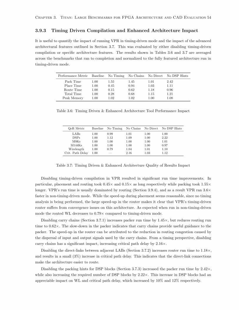
Chapter 3. Titan: Large Benchmarks for FPGA Architecture and CAD Evaluation 54
3.9.3 Timing Driven Compilation and Enhanced Architecture Impact
It is useful to quantify the impact of running VPR in timing-driven mode and the impact of the advanced
architectural features outlined in Section 3.7. This was evaluated by either disabling timing-driven
compilation or specific architecture features. The results shown in Tables 3.6 and 3.7 are averaged
across the benchmarks that ran to completion and normalized to the fully featured architecture run in
timing-driven mode.
Performance Metric Baseline No Timing No Chains No Direct No DSP Hints
Pack Time 1.00 1.55 1.45 1.01 2.42Place Time 1.00 0.45 0.94 1.03 1.11Route Time 1.00 0.15 0.62 1.18 0.96Total Time 1.00 0.28 0.68 1.15 1.21
Peak Memory 1.00 1.02 1.02 1.00 1.08
Table 3.6: Timing Driven & Enhanced Architecture Tool Performance Impact
QoR Metric Baseline No Timing No Chains No Direct No DSP Hints
LABs 1.00 0.99 1.01 1.00 1.00DSPs 1.00 1.12 1.09 1.00 2.22M9Ks 1.00 1.00 1.00 1.00 1.01
M144Ks 1.00 1.00 1.00 1.00 0.97Wirelength 1.00 0.79 1.04 1.01 1.10
Crit. Path Delay 1.00 — 2.16 1.03 1.12
Table 3.7: Timing Driven & Enhanced Architecture Quality of Results Impact
Disabling timing-driven compilation in VPR resulted in significant run time improvements. In
particular, placement and routing took 0.45× and 0.15× as long respectively while packing took 1.55×longer. VPR’s run time is usually dominated by routing (Section 3.9.4), and as a result VPR ran 3.6×faster in non-timing-driven mode. While the speed-up during placement seems reasonable, since no timing
analysis is being performed, the large speed-up in the router makes it clear that VPR’s timing-driven
router suffers from convergence issues on this architecture. As expected when run in non-timing-driven
mode the routed WL decreases to 0.79× compared to timing-driven mode.
Disabling carry chains (Section 3.7.1) increases packer run time by 1.45×, but reduces routing run
time to 0.62×. The slow-down in the packer indicates that carry chains provide useful guidance to the
packer. The speed-up in the router can be attributed to the reduction in routing congestion caused by
the dispersal of input and output signals used by the carry chains. From a timing perspective, disabling
carry chains has a significant impact, increasing critical path delay by 2.16×.
Disabling the direct-links between adjacent LABs (Section 3.7.2) increases router run time to 1.18×,
and results in a small (3%) increase in critical path delay. This indicates that the direct-link connections
make the architecture easier to route.
Disabling the packing hints for DSP blocks (Section 3.7.3) increased the packer run time by 2.42×,
while also increasing the required number of DSP blocks by 2.22×. This increase in DSP blocks had an
appreciable impact on WL and critical path delay, which increased by 10% and 12% respectively.

Chapter 3. Titan: Large Benchmarks for FPGA Architecture and CAD Evaluation 55
Name Total Blocks Pack Place Route Total Mem. Outcome
gaussianblur * 1,859,485 745.8 ERRbitcoin miner * 1,061,829 248.1 (2.38×) 427.7 (0.35×) UNR
directrf * 934,490 ERRsparcT1 chip2 † 824,152 76.8 (1.01×) 117.1 (0.47×) 568.7 762.6 46.0LU Network † 630,103 48.2 (1.45×) 113.1 (0.84×) OOT
LU230 * 567,992 148.3 (1.82×) OOMmes noc † 549,045 53.2 (2.84×) 117.2 (1.21×) 433.0 (7.90×) 603.4 (2.72×) 39.0 (5.42×)
gsm switch * 491,846 85.3 (1.94×) 204.1 (1.07×) OOTdenoise 342,899 39.8 (3.01×) 111.8 (1.21×) 1,335.7 (27.86×) 1,487.4 (8.14×) 25.0 (4.60×)
sparcT2 core 288,005 37.0 (3.33×) 50.1 (0.71×) 348.3 (9.16×) 435.4 (3.06×) 18.0 (4.58×)cholesky bdti 256,072 16.6 (1.51×) 32.0 (0.77×) 188.2 (12.17×) 236.8 (2.67×) 25.0 (6.78×)
minres † 252,454 13.8 (1.76×) 20.9 (0.65×) 135.4 (9.28×) 170.1 (2.38×) 42.0 (9.96×)stap qrd 237,197 15.3 (1.04×) 47.1 (1.31×) 86.7 (7.05×) 149.0 (1.83×) 23.0 (6.65×)openCV † 212,615 14.2 (2.63×) 20.9 (0.84×) OOT
dart 202,368 17.7 (2.34×) 20.6 (0.73×) OOTbitonic mesh † 191,664 19.2 (3.87×) 28.2 (0.91×) 1,914.9 (20.02×) 1,962.3 (12.86×) 55.0 (11.63×)segmentation 167,917 17.1 (3.07×) 37.4 (0.99×) 546.1 (22.30×) 600.5 (7.30×) 17.0 (5.61×)SLAM spheric 125,194 12.0 (2.90×) 22.2 (0.98×) OOT
des90 † 109,811 9.3 (4.22×) 12.4 (0.80×) 228.6 (5.61×) 250.3 (3.63×) 28.0 (9.29×)cholesky mc 108,236 6.1 (1.94×) 10.2 (0.85×) 30.4 (4.74×) 46.6 (1.34×) 16.0 (6.90×)stereo vision 92,662 3.3 (1.27×) 8.0 (0.69×) 11.1 (3.31×) 22.4 (0.96×) 9.2 (5.30×)sparcT1 core 91,268 9.8 (3.77×) 8.7 (0.85×) 46.0 (3.61×) 64.5 (1.94×) 7.1 (3.89×)
neuron 90,778 4.6 (1.90×) 7.4 (0.71×) 19.6 (3.46×) 31.5 (1.08×) 10.0 (4.63×)
Geomean 26.4 (2.20×) 36.3 (0.81×) 171.0 (8.23×) 229.4 (2.82×) 21.8 (6.21×)
ERR: Error in VPR. UNR: Unroute. OOT: Out of Time (>48 hours). OOM: Out of Memory (>128 GiB).*Run on 128 GiB machine. †Run on 64 GiB machine.
Table 3.8: VPR 7 run time in minutes and memory in GiB. Relative speed to Quartus II (VPR/Q2) isshown in parentheses.
3.9.4 Performance Comparison with Quartus II
Table 3.8 shows both the absolute run time and peak memory of VPR, and the relative values compared
to Quartus II on the Titan23 benchmark suite, using the enhanced architecture. Quartus II’s absolute run
time and peak memory across the same benchmarks, while targeting Stratix IV, are shown in Table 3.9.
Both tools were run in timing-driven mode.
VPR spends most of its time on routing, which takes on average 80% of the total run time on
benchmarks that completed. In contrast, Quartus II has a more even run time distribution with
placement taking the largest amount of time (38%), and with a significant amount of time (28% and
25%) spent on routing and miscellaneous actions respectively. For both tools, run time can be quite
substantial on larger benchmarks, taking in excess of 48 hours2. Looking at the relative run time of the
two tools in Table 3.8, we can gain additional insights into each step of the CAD flow.
Packing is slower (2.2×) in VPR than in Quartus II, which can be partly attributed to VPR’s more
flexible packer, which allows it to target a wide range of FPGA architectures.
On average, both VPR and Quartus II spend a comparable amount of time during placement, with
VPR using 19% less execution time. However this is somewhat pessimistic for VPR, since it also spends
time generating the delay map used for placement, while Quartus II uses a pre-computed device delay
model. This is an example of where VPR has additional overhead because of its architecture independence.
Additionally, VPR typically uses fewer LABs than Quartus II (see Section 3.9.5), which decreases the
size of VPR’s placement problem. Quartus II also enforces stricter placement legality constraints and
uses more intelligent directed moves than VPR, which also affect its run time [51].
VPR’s timing-driven router is also substantially slower (8.2×) than Quartus II’s. Furthermore, the
router’s run time is volatile, ranging from 3.3× slower in the best case to nearly 28× slower in the worst
2In contrast, the largest MCNC20 circuit took 60s in VPR and 65s in Quartus II, highlighting the importance of usinglarge benchmarks to evaluate CAD tools.

Chapter 3. Titan: Large Benchmarks for FPGA Architecture and CAD Evaluation 56
Name Total Blocks Pack Place Route Misc. Total Mem. Outcome
gaussianblur * 1,859,485 DEVbitcoin miner * 1,061,829 104.1 1,226.8 2,387.6 337.5 4,379.9 10.5
directrf * 934,490 DEVsparcT1 chip2 * 824,152 76.3 251.3 OOTLU Network * 630,103 33.2 134.7 85.4 57.3 300.2 8.4
LU230 * 567,992 81.6 290.1 211.3 122.7 823.5 9.5mes noc * 549,045 18.7 96.6 54.8 63.4 222.2 7.2
gsm switch * 491,846 44.0 190.7 266.0 40.1 579.2 7.0denoise 342,899 13.2 92.4 48.0 29.1 182.6 5.4
sparcT2 core 288,005 11.1 70.1 38.0 23.1 142.4 3.9cholesky bdti 256,072 11.0 41.5 15.5 20.9 88.8 3.7
minres * 252,454 7.9 32.1 14.6 20.6 71.4 4.2stap qrd 237,197 14.7 35.9 12.3 18.7 81.6 3.5openCV * 212,615 5.4 24.8 11.6 15.9 54.8 3.7
dart 202,368 7.6 28.0 23.9 741.9 801.3 3.2bitonic mesh * 191,664 5.0 31.0 95.7 25.6 152.6 4.7segmentation 167,917 5.6 37.8 24.5 14.4 82.2 3.0SLAM spheric 125,194 4.2 22.7 16.2 13.0 56.1 2.6
des90 * 109,811 2.2 15.5 40.7 12.8 69.0 3.0cholesky mc 108,236 3.1 11.9 6.4 13.3 34.8 2.3stereo vision 92,662 2.6 11.6 3.4 5.9 23.4 1.7sparcT1 core 91,268 2.6 10.3 12.8 7.6 33.3 1.8
neuron 90,778 2.4 10.4 5.7 10.9 29.3 2.2
Geomean 10.3 48.9 32.8 28.8 133.4 4.0
DEV: Exceeded size of largest Stratix IV device. OOT: Out of Time (>48 hours).*Run time scaled to 64 GiB or 128 GiB machine.
Table 3.9: Quartus II run time in minutes and memory in GiB.
case. This can be partly attributed to VPR’s default congestion resolution schedule, which increases the
cost of overused resources slowly with the aim of achieving low critical path delay.
As to overall run time, for benchmarks it successfully fits, VPR takes 2.8× longer that Quartus II.
However, it should be noted that this result is skewed in VPR’s favour, since it does not account for
benchmarks which did not complete. Peak memory consumption is also much higher (6.2×) in VPR.
This is quite significant and will often limit the design sizes VPR can handle. It is interesting to note that
the largest benchmark that Quartus II will fit (bitcoin miner), uses approximately the same memory in
Quartus II as the smallest Titan23 benchmark (neuron) uses in VPR.
It is also useful to compare the scalability of VPR and Quartus II with design size, since scalable
CAD tools are required to continue exploiting Moore’s Law. As shown in Table 3.8, VPR is unable to
complete at least 6 of the benchmarks due to either excessive memory or run time. Quartus II in contrast,
completes all but one of the benchmarks that fit on Stratix IV devices (Table 3.9). Furthermore, when
considering total run time VPR is closest (1.0×-1.9×) to Quartus II on the four smallest benchmarks,
but generally falls behind as design size increases. From these results it appears that Quartus II scales
better than VPR as design size increases.
These results are notably different from those previously reported for wire length driven optimization
in [29]. The most significant difference is that VPR’s run time is now spent primarily during routing,
rather than during packing. This is attributable to two main factors. First, VPR’s packing performance
has been significantly improved due to recent algorithmic enhancements and the addition of packing
hints (Section 3.7.3). Second, VPR’s timing-driven router is significantly slower (Section 3.9.3) than the
wire length driven router, often requiring significantly more routing iterations to resolve congestion. We
observed that VPR spends a large number of later routing iterations attempting to resolve congestion on

Chapter 3. Titan: Large Benchmarks for FPGA Architecture and CAD Evaluation 57
only a handful of overused routing resources, which were always logic block output pins. Additionally, we
found that small tweaks to the router cost parameters or architecture can cause large variations in the
timing-driven router’s run time.
3.9.5 Quality of Results Comparison with Quartus II
The relative QoR results for the Titan23 benchmark suite are shown in Table 3.10. These results show
several trends. First, VPR uses fewer LABs (0.8×) than Quartus II. While this reduced LAB usage may
initially seem a benefit (since a smaller FPGA could be used), this comes at the cost of WL as will be
discussed in Section 3.9.6.
Name Total Blocks LAB DSP M9K M144K WL Crit. Path
gaussianblur 1,859,485bitcoin miner 1,061,829 0.89 0.91 3.45 3.85 *
directrf 934,490sparcT1 chip2 824,152LU Network 630,103 1.38 1.00 1.26 2.86 *
LU230 567,992 0.53 1.00 3.57 21.38mes noc 549,045 0.84 1.00 1.97 1.37
gsm switch 491,846 0.65 1.48 2.38 *denoise 342,899 0.73 1.50 2.66 1.77 1.02
sparcT2 core 288,005 0.92 1.00 1.43 1.51cholesky bdti 256,072 1.03 1.02 1.00 2.58 1.87
minres 252,454 0.61 1.49 1.00 2.69 1.59stap qrd 237,197 1.75 0.99 0.76 2.81 2.52openCV 212,615 0.78 1.31 1.15 1.00 3.30 *
dart 202,368 0.72 0.93 2.26 *bitonic mesh 191,664 0.65 0.77 0.96 1.94 1.77 1.77segmentation 167,917 0.70 1.17 1.32 2.50 1.76 1.10SLAM spheric 125,194 0.66 1.09 1.52 *
des90 109,811 0.67 0.56 0.95 1.70 1.33cholesky mc 108,236 0.87 0.98 1.10 1.00 2.43 2.44stereo vision 92,662 0.71 4.00 1.11 2.24 1.21sparcT1 core 91,268 0.89 1.00 1.01 1.31 1.16
neuron 90,778 0.70 0.82 1.65 2.61 1.84
Geomean 0.80 1.12 1.20 2.67 2.19 1.53
* VPR WL scaled from placement estimate.
Table 3.10: VPR 7/Quartus II Quality of Result Ratios.
Looking at the other block types, VPR uses 1.1× as many DSP blocks and 1.2× as many M9K blocks
as Quartus II, showing that Quartus II is somewhat better at utilizing these hard block resources. Since
only six circuits use M144K blocks in both tools, it is difficult to draw meaningful conclusions.
Routed WL is one of the key metrics for comparing the overall quality of VPR and Quartus II.
Somewhat surprisingly, the wire length gap is quite large, with VPR using 2.2× more wire than Quartus
II3. Without access to Quartus II’s internal packing, placement and routing statistics, it is difficult to
identify which steps of the design flow are responsible for this difference. However, as will be shown
in Section 3.9.6 VPR’s packing quality has a significant impact. In addition, it is likely that Quartus
3The WL gap is quite different (0.7×) on the largest MCNC20 circuit, emphasizing how modern benchmarks can impactCAD tool QoR.
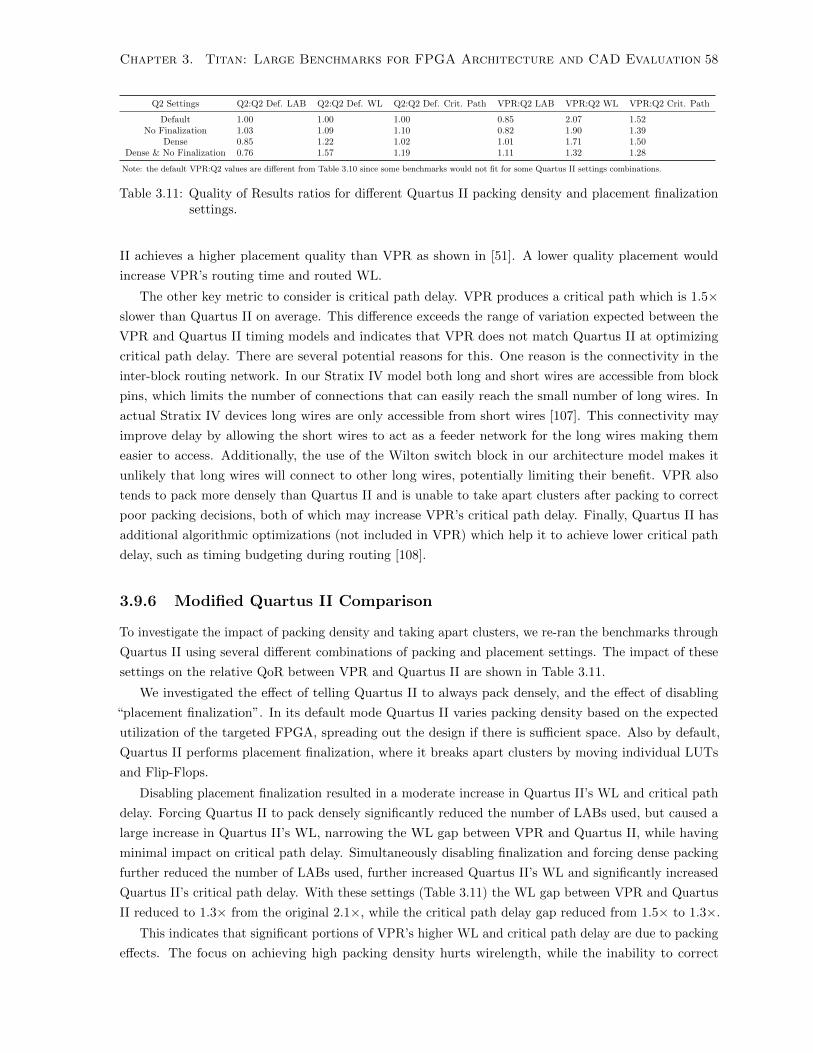
Chapter 3. Titan: Large Benchmarks for FPGA Architecture and CAD Evaluation 58
Q2 Settings Q2:Q2 Def. LAB Q2:Q2 Def. WL Q2:Q2 Def. Crit. Path VPR:Q2 LAB VPR:Q2 WL VPR:Q2 Crit. Path
Default 1.00 1.00 1.00 0.85 2.07 1.52No Finalization 1.03 1.09 1.10 0.82 1.90 1.39
Dense 0.85 1.22 1.02 1.01 1.71 1.50Dense & No Finalization 0.76 1.57 1.19 1.11 1.32 1.28
Note: the default VPR:Q2 values are different from Table 3.10 since some benchmarks would not fit for some Quartus II settings combinations.
Table 3.11: Quality of Results ratios for different Quartus II packing density and placement finalizationsettings.
II achieves a higher placement quality than VPR as shown in [51]. A lower quality placement would
increase VPR’s routing time and routed WL.
The other key metric to consider is critical path delay. VPR produces a critical path which is 1.5×slower than Quartus II on average. This difference exceeds the range of variation expected between the
VPR and Quartus II timing models and indicates that VPR does not match Quartus II at optimizing
critical path delay. There are several potential reasons for this. One reason is the connectivity in the
inter-block routing network. In our Stratix IV model both long and short wires are accessible from block
pins, which limits the number of connections that can easily reach the small number of long wires. In
actual Stratix IV devices long wires are only accessible from short wires [107]. This connectivity may
improve delay by allowing the short wires to act as a feeder network for the long wires making them
easier to access. Additionally, the use of the Wilton switch block in our architecture model makes it
unlikely that long wires will connect to other long wires, potentially limiting their benefit. VPR also
tends to pack more densely than Quartus II and is unable to take apart clusters after packing to correct
poor packing decisions, both of which may increase VPR’s critical path delay. Finally, Quartus II has
additional algorithmic optimizations (not included in VPR) which help it to achieve lower critical path
delay, such as timing budgeting during routing [108].
3.9.6 Modified Quartus II Comparison
To investigate the impact of packing density and taking apart clusters, we re-ran the benchmarks through
Quartus II using several different combinations of packing and placement settings. The impact of these
settings on the relative QoR between VPR and Quartus II are shown in Table 3.11.
We investigated the effect of telling Quartus II to always pack densely, and the effect of disabling
“placement finalization”. In its default mode Quartus II varies packing density based on the expected
utilization of the targeted FPGA, spreading out the design if there is sufficient space. Also by default,
Quartus II performs placement finalization, where it breaks apart clusters by moving individual LUTs
and Flip-Flops.
Disabling placement finalization resulted in a moderate increase in Quartus II’s WL and critical path
delay. Forcing Quartus II to pack densely significantly reduced the number of LABs used, but caused a
large increase in Quartus II’s WL, narrowing the WL gap between VPR and Quartus II, while having
minimal impact on critical path delay. Simultaneously disabling finalization and forcing dense packing
further reduced the number of LABs used, further increased Quartus II’s WL and significantly increased
Quartus II’s critical path delay. With these settings (Table 3.11) the WL gap between VPR and Quartus
II reduced to 1.3× from the original 2.1×, while the critical path delay gap reduced from 1.5× to 1.3×.
This indicates that significant portions of VPR’s higher WL and critical path delay are due to packing
effects. The focus on achieving high packing density hurts wirelength, while the inability to correct
Chapter 3. Titan: Large Benchmarks for FPGA Architecture and CAD Evaluation 59
AB
(a) Dense Packing
AB
(b) Less Dense Packing
Figure 3.5: Packing density example.
poor packing decisions (no placement finalization) hurts critical path delay. Together these settings
have an even larger impact. We suspect that VPR’s packer is sometimes packing largely unrelated logic
together to minimize the number of clusters. This appears to be counter productive from a WL and
delay perspective.
For example, consider a LAB (Figure 3.5a) that is mostly filled with related logic A, but which can
accommodate an extra unrelated register B. During placement, the cost of moving this LAB will be
dominated by the connectivity to the related logic A. This could result in a final position that is good
for A but may be very poor for the extra register B (i.e. far from its related logic). If this is a common
occurrence it could lead to increased WL and critical path delay.
A better solution (Figure 3.5b) would have been to utilize additional clusters (pack less densely) to
avoid packing unrelated logic together. Alternately, if the placement engine was able to recognize the
competing connectivity requirements inside a cluster, it could break it apart, much like Quartus II’s
placement finalization. These results agree with those presented in [109], which showed that the routing
demand (as measured by the minimum channel width required to route a design) could be significantly
decreased by packing logic blocks less densely.
3.9.7 Comparison of VPR to Other Commercial Tools
In [95] VPR packing and placement were compared to Xilinx’s ISE tool on four VTR benchmarks. Similar
to our results, the authors found that VPR produced a denser packing than ISE, had slower critical paths,
used more routing resources, took more execution time and required more memory. Despite differences
in methodology and tools, the general conclusion is the same — VPR does not optimize as well, and
requires more computational resources than commercial CAD tools.
3.9.8 VPR versus Quartus II Quality Implications
It is clear from the previously presented results that Quartus II outperforms VPR in terms of QoR,
performance and scalability. However, it may be argued that this is not surprising. VPR is used
primarily as an academic research platform, and as a result is capable of targeting a wide range of
FPGA architectures. Quartus II in contrast, is used for FPGA design implementation on real devices
and targets the narrower set of Altera FPGA architectures. This means additional optimizations can be
Chapter 3. Titan: Large Benchmarks for FPGA Architecture and CAD Evaluation 60
made in Quartus II, for both QoR and tool performance, which may not be possible (or have not been
implemented) in VPR.
It is important, however, that this gap not be too large. Given the empirical nature of most FPGA
CAD and architecture research, research conclusions can become dependant on the CAD tools used [91].
In order to be confident in research conclusions, it is important for CAD tools such as VPR to remain at
least reasonably comparable to state-of-the-art commercial tools.
3.10 Conclusion
First, we have presented Titan, a hybrid CAD flow that enables the creation of large benchmark circuits
for use in academic CAD tools, supporting a wide variety of HDLs and range of IP blocks. Second,
we have presented the Titan23 benchmark suite built using the Titan flow. The Titan23 benchmarks
significantly improve the state of open-source FPGA benchmarks by providing designs across a wide
range of application domains, which are much closer in both size and style to modern FPGA usage.
Third, we have presented a detailed architecture capture, including a correlated timing model, of Altera’s
Stratix IV family. As a modern high performance FPGA architecture, this forms a useful baseline for the
evaluation of CAD or architecture changes. Finally, we have used this benchmark suite and architecture
capture to compare the popular academic CAD tool VPR with a state-of-the-art commercial CAD tool,
Altera’s Quartus II. The results show that VPR is at least 2.8× slower, consumes 6.2× more memory,
uses 2.2× more wire, and produces critical paths 1.5× slower than Quartus II. Additional investigation
identified VPR’s focus on achieving high packing density and inability to take apart clusters to be an
important factors in the WL and critical path delay differences. VPR’s timing driven router also suffered
from convergence issues which increased routing run time. These results show that current CAD tools,
both academic and commercial, suffer from scalability challenges (both VPR and Quartus II were unable
to complete some benchmarks in less than 48 hours). As a result scalable CAD flows remain an important
area for future research.
It is possible with large designs, that CAD tools may benefit from additional guidance, such as a
system-level floorplan. We investigate floorplanning with the Titan23 benchmarks in Chapter 5.

Chapter 4
Latency Insensitive Communication
on FPGAs
The whole tendency of modern communication [. . . ] is towards participation in a
process.
— Marshall McLuhan
4.1 Introduction
One of the challenges associated with a divide-and-conquer approach to digital systems design is handling
the tight coupling of timing constraints between the divided components. Latency Insensitive Design
(LID) offers a way to decouple the timing requirements between modules, which helps facilitate a
divide-and-conquer approach.
LID has the potential to reduce the number of design iterations required to achieve timing closure by
allowing timing critical links to be pipelined late in the design flow. However, there are several open
questions regarding Latency Insensitive (LI) methodologies that have not been well addressed by previous
research. This chapter attempts to provide guidelines to designers interested in LI approaches and address
the following questions:
• What are the area and frequency overheads of LID on FPGAs?
• What are the potential frequency limitations in LI systems and what optimization can be applied
to improve operating frequency?
• How effective is LI pipelining? How does it compare to conventional (non-LI) pipelining?
• How should LI communication granularity be chosen to produce area-efficient LI systems?
4.2 Latency Insensitive Design Implementation
In order to quantify the costs of a LI design methodology we have created a set of LI wrappers and
relay stations based on those presented in [110] and implemented them on Stratix IV FPGAs. Example
wrappers are shown in Figure 4.1.
61

Chapter 4. Latency Insensitive Communication on FPGAs 62
0
1
fire
deqenq
valid
clk
in_dataout_data
out_stop
out_valid
stop
in_valid
PearlFIFO
in_stop
Shell
empty
deq
enq
full
alm
st_full
fire
ena
(a) Baseline latency insensitive wrapper (one input, oneoutput). Critical paths highlighted in red.
0
1
fire
deqenq
valid
clk
in_dataout_data
out_stop
out_valid
stop
in_valid
PearlFIFO
in_stop
Shell
empty
deq
enq
full
alm
st_full
fire
ena
(b) Optimized latency insensitive wrapper (one input,one output). Additional registers added in the opti-mized version shown in dashed-blue.
Figure 4.1: Latency insensitive wrapper implementations.
1
0
aux
valid
in_data
in_valid
1
0
0
out_valid
main
sel
ena
out_data
cntrl
in_stop
out_stopaux_ena
sta
te
Relay Station
Figure 4.2: Latency insensitive relay station
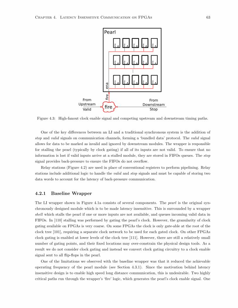
Chapter 4. Latency Insensitive Communication on FPGAs 63
ena
firefire
ena
ena
ena
ena
ena
ena
ena
ena
ena
ena
ena
ena
ena
ena
ena
...
Pearl
From Upstream
FromDownstream
Valid Stop
Figure 4.3: High-fanout clock enable signal and competing upstream and downstream timing paths.
One of the key differences between an LI and a traditional synchronous system is the addition of
stop and valid signals on communication channels, forming a ‘bundled data’ protocol. The valid signal
allows for data to be marked as invalid and ignored by downstream modules. The wrapper is responsible
for stalling the pearl (typically by clock gating) if all of its inputs are not valid. To ensure that no
information is lost if valid inputs arrive at a stalled module, they are stored in FIFOs queues. The stop
signal provides back-pressure to ensure the FIFOs do not overflow.
Relay stations (Figure 4.2) are used in place of conventional registers to perform pipelining. Relay
stations include additional logic to handle the valid and stop signals and must be capable of storing two
data words to account for the latency of back-pressure communication.
4.2.1 Baseline Wrapper
The LI wrapper shown in Figure 4.1a consists of several components. The pearl is the original syn-
chronously designed module which is to be made latency insensitive. This is surrounded by a wrapper
shell which stalls the pearl if one or more inputs are not available, and queues incoming valid data in
FIFOs. In [110] stalling was performed by gating the pearl’s clock. However, the granularity of clock
gating available on FPGAs is very coarse. On some FPGAs the clock is only gate-able at the root of the
clock tree [101], requiring a separate clock network to be used for each gated clock. On other FPGAs
clock gating is enabled at lower levels of the clock tree [111]. However, there are still a relatively small
number of gating points, and their fixed locations may over-constrain the physical design tools. As a
result we do not consider clock gating and instead we convert clock gating circuitry to a clock enable
signal sent to all flip-flops in the pearl.
One of the limitations we observed with the baseline wrapper was that it reduced the achievable
operating frequency of the pearl module (see Section 4.3.1). Since the motivation behind latency
insensitive design is to enable high speed long distance communication, this is undesirable. Two highly
critical paths run through the wrapper’s ‘fire’ logic, which generates the pearl’s clock enable signal. One

Chapter 4. Latency Insensitive Communication on FPGAs 64
path comes from an upstream module’s valid signal and the other from a downstream module’s stop
signal (see Figure 4.3). Since each path attempts to pull the logic in opposite directions, it forces the CAD
tools to produce a compromise solution with decreased operating frequency. This is further exacerbated
by the high fan-out of the clock enable signal. For the relatively small modules presented in Section 4.3.1,
the clock enable fanned-out to nearly 1400 registers.
One of the largest components of LI wrappers are the FIFOs input queues. To avoid unnecessary
stalls these FIFOs require single cycle read/write capability, single cycle updates to full and empty signals
and ‘new data’ behaviour when a write and read occur at the same address (i.e. the read receives the
new data being written). The ‘new data’ behaviour required additional logic to be inferred around the
RAM elements since this mode of operation is not natively supported by the Stratix IV RAM blocks.
While it was possible to infer the FIFOs into the MLAB/LUTRAM structures on Stratix IV FPGAs,
the choice was left to the CAD tool, which usually implemented them as M9K RAM blocks. Adding
native support for ‘new data’ behaviour in future FPGA RAM blocks would help reduce the overhead
associated with these FIFOs.
4.2.2 Optimized Wrapper
To improve the frequency limitations of the baseline wrapper, we created an improved wrapper by inserting
an additional register after the fire logic as shown in Figure 4.1b. This breaks the long combinational paths
before they became high fan-out and greatly improved achievable frequency. However this required several
changes to the wrapper architecture. To ensure that all components remained correctly synchronized with
the clock enable signal, additional registers also had to be inserted after the FIFO bypass mux and valid
signal generation logic. This introduces one extra cycle of round-trip communication latency between
modules. The FIFO must reserve an additional word to handle the possibility of an additional data word
in flight. We attempted to further pipeline the LI wrapper but it resulted in only marginal improvement.
4.3 Results
To evaluate the cost and overhead of LID, we created a program to automatically generate LI wrappers
based on a Verilog module description1. This program was used to generate wrappers for a design
consisting of cascaded FIR filters, and also to more generally investigate the scalability of LI wrappers.
All area and frequency results were determined by implementing the design with Altera’s Quartus
II CAD tool (version 12.1) targeting the fastest speed grade of Stratix IV devices. To compare area
between implementations that make use of hardened blocks (e.g. DSPs and RAM blocks), we calculate
‘equivalent Logic Array Blocks (LABs)’ based on the normalized block sizes from [112]. Since Quartus II
may purposefully spread out the design soft logic and registers for timing purposes (inflating the number
of LABs used), we calculate the required number of LABs by dividing the number of required LUT+FF
pairs by the number of pairs per LAB.
1The program, along with the LI wrappers and relay stations are available from: http://www.eecg.utoronto.ca/
~vaughn/software.html
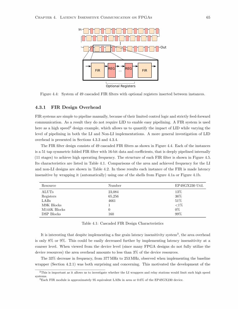
Chapter 4. Latency Insensitive Communication on FPGAs 65
FIRREG REG
... FIR
In
Out
Optional Registers
...
Figure 4.4: System of 49 cascaded FIR filters with optional registers inserted between instances.
4.3.1 FIR Design Overhead
FIR systems are simple to pipeline manually, because of their limited control logic and strictly feed-forward
communication. As a result they do not require LID to enable easy pipelining. A FIR system is used
here as a high speed2 design example, which allows us to quantify the impact of LID while varying the
level of pipelining in both the LI and Non-LI implementations. A more general investigation of LID
overhead is presented in Sections 4.3.3 and 4.3.4.
The FIR filter design consists of 49 cascaded FIR filters as shown in Figure 4.4. Each of the instances
is a 51 tap symmetric folded FIR filter with 16-bit data and coefficients, that is deeply pipelined internally
(11 stages) to achieve high operating frequency. The structure of each FIR filter is shown in Figure 4.5.
Its characteristics are listed in Table 4.1. Comparisons of the area and achieved frequency for the LI
and non-LI designs are shown in Table 4.2. In these results each instance of the FIR is made latency
insensitive by wrapping it (automatically) using one of the shells from Figure 4.1a or Figure 4.1b.
Resource Number EP4SGX230 Util.
ALUTs 23,084 13%Registers 65,256 36%LABs 4661 51%M9K Blocks 1 <1%M144K Blocks 0 0%DSP Blocks 160 99%
Table 4.1: Cascaded FIR Design Characteristics
It is interesting that despite implementing a fine grain latency insensitivity system3, the area overhead
is only 8% or 9%. This could be easily decreased further by implementing latency insensitivity at a
coarser level. When viewed from the device level (since many FPGA designs do not fully utilize the
device resources) the area overhead amounts to less than 3% of the device resources.
The 33% decrease in frequency, from 377 MHz to 253 MHz, observed when implementing the baseline
wrapper (Section 4.2.1) was both surprising and concerning. This motivated the development of the
2This is important as it allows us to investigate whether the LI wrappers and relay stations would limit such high speedsystems.
3Each FIR module is approximately 95 equivalent LABs in area or 0.6% of the EP4SGX230 device.

Chapter 4. Latency Insensitive Communication on FPGAs 66
DSP Block
+
x
h[25]
x
h[26]
+in[N-25]
in[N-27]
in[N-26]
+in[N]
in[N-51]
+in[N-1]
in[N-50]
+in[N-2]
in[N-49]
+in[N-3]
in[N-48]
+in[N-4]
in[N-47]
+in[N-5]
in[N-46]
+in[N-6]
in[N-45]
+in[N-7]
in[N-44]
+
+
x
h[0]
x
h[1]
+
x
h[2]
x
h[3]
+
+
+
x
h[4]
x
h[5]
+
x
h[6]
x
h[7]
+
'0'
DSP Block
...
+
+ out[N]
1 Cycle 4 Cycles 6 Cycles
+
Figure 4.5: FIR filter architecture. Number of clock cycles required by each portion of the design areannotated.
Resource Non-LI Base LI Opt. LI
LUT+FF Pairs 54,940 60,086 (1.09×) 60,299 (1.10×)DSP Blocks 160 160 (1.00×) 160 (1.00×)
M9K 1 49 (49.00×) 49 (49.00×)M144K 0 0 0
Equiv. LABs 4,654 5,049 (1.08×) 5,060 (1.09×)Fmax [MHz] 377 253 (0.67×) 348 (0.92×)
Table 4.2: Post fit resource usage and operating frequency for the cascaded FIR design using differentcommunication styles. Values normalized to non-LI system are shown in parenthesis.
optimized wrapper (Section 4.2.2) which improved frequency to 348 MHz, only 8% below the latency-
sensitive system. While this is still a notable impact compared to the non-LI system, it is significantly
lower than the baseline wrapper, and comes at only a marginal increase in area overhead.
It was also informative to compare what level of pipelining was required between filter instances when
using the LI wrappers to achieve an operating frequency comparable to the non-LI system. As shown in
Figure 4.4 additional pipeline registers (or relay stations) are inserted between FIR filter instances. A
summary of these results is shown in Figure 4.6 for various sizes of the cascaded FIR filter design. The
first thing to note is the downward trend in operating frequency associated with increasing design size for
all design styles. This is an artifact of the imperfect nature of the CAD tools used to implement the
design. The design is highly pipelined, with no combinational paths between instances. Despite finding
a high speed (510 MHz) implementation with one instance in the non-LI system (Non-LI 0 REG) the
quality decreases as the design size increases, resulting in a 26% drop in operating frequency when scaling
from one to 49 instances. The magnitude of this effect also varies between implementations. For the
baseline LI wrapper (LI 0 RS Base.) the frequency dropped 42% across the same range. This disparity
is likely a result of the different difficulties these implementations present to the CAD tool, with the
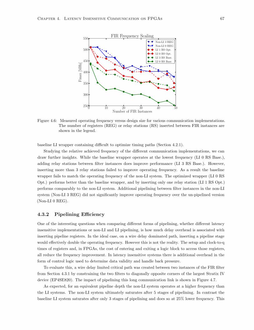
Chapter 4. Latency Insensitive Communication on FPGAs 67
0 10 20 30 40 50Number of FIR Instances
250
300
350
400
450
500
550
Fm
ax[M
Hz]
FIR Frequency ScalingNon-LI 3 REG
Non-LI 0 REG
LI 1 RS Opt.
LI 0 RS Opt.
LI 3 RS Base.
LI 0 RS Base.
Figure 4.6: Measured operating frequency versus design size for various communication implementations.The number of registers (REG) or relay stations (RS) inserted between FIR instances areshown in the legend.
baseline LI wrapper containing difficult to optimize timing paths (Section 4.2.1).
Studying the relative achieved frequency of the different communication implementations, we can
draw further insights. While the baseline wrapper operates at the lowest frequency (LI 0 RS Base.),
adding relay stations between filter instances does improve performance (LI 3 RS Base.). However,
inserting more than 3 relay stations failed to improve operating frequency. As a result the baseline
wrapper fails to match the operating frequency of the non-LI system. The optimized wrapper (LI 0 RS
Opt.) performs better than the baseline wrapper, and by inserting only one relay station (LI 1 RS Opt.)
performs comparably to the non-LI system. Additional pipelining between filter instances in the non-LI
system (Non-LI 3 REG) did not significantly improve operating frequency over the un-pipelined version
(Non-LI 0 REG).
4.3.2 Pipelining Efficiency
One of the interesting questions when comparing different forms of pipelining, whether different latency
insensitive implementations or non-LI and LI pipelining, is how much delay overhead is associated with
inserting pipeline registers. In the ideal case, on a wire delay dominated path, inserting a pipeline stage
would effectively double the operating frequency. However this is not the reality. The setup and clock-to-q
times of registers and, in FPGAs, the cost of entering and exiting a logic block to access those registers,
all reduce the frequency improvement. In latency insensitive systems there is additional overhead in the
form of control logic used to determine data validity and handle back pressure.
To evaluate this, a wire delay limited critical path was created between two instances of the FIR filter
from Section 4.3.1 by constraining the two filters to diagonally opposite corners of the largest Stratix IV
device (EP4SE820). The impact of pipelining this long communication link is shown in Figure 4.7.
As expected, for an equivalent pipeline depth the non-LI system operates at a higher frequency than
the LI systems. The non-LI system ultimately saturates after 5 stages of pipelining. In contrast the
baseline LI system saturates after only 3 stages of pipelining and does so at 25% lower frequency. This
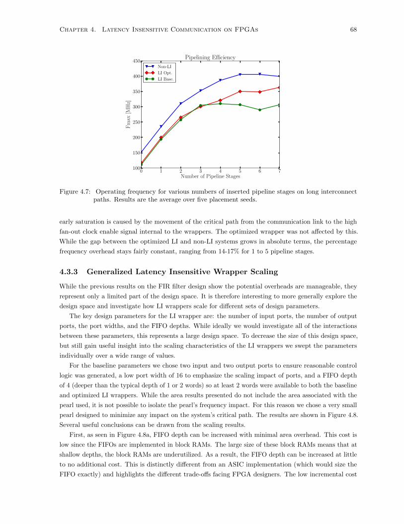
Chapter 4. Latency Insensitive Communication on FPGAs 68
0 1 2 3 4 5 6 7Number of Pipeline Stages
100
150
200
250
300
350
400
450
Fm
ax[M
Hz]
Pipelining Efficiency
Non-LI
LI Opt.
LI Base.
Figure 4.7: Operating frequency for various numbers of inserted pipeline stages on long interconnectpaths. Results are the average over five placement seeds.
early saturation is caused by the movement of the critical path from the communication link to the high
fan-out clock enable signal internal to the wrappers. The optimized wrapper was not affected by this.
While the gap between the optimized LI and non-LI systems grows in absolute terms, the percentage
frequency overhead stays fairly constant, ranging from 14-17% for 1 to 5 pipeline stages.
4.3.3 Generalized Latency Insensitive Wrapper Scaling
While the previous results on the FIR filter design show the potential overheads are manageable, they
represent only a limited part of the design space. It is therefore interesting to more generally explore the
design space and investigate how LI wrappers scale for different sets of design parameters.
The key design parameters for the LI wrapper are: the number of input ports, the number of output
ports, the port widths, and the FIFO depths. While ideally we would investigate all of the interactions
between these parameters, this represents a large design space. To decrease the size of this design space,
but still gain useful insight into the scaling characteristics of the LI wrappers we swept the parameters
individually over a wide range of values.
For the baseline parameters we chose two input and two output ports to ensure reasonable control
logic was generated, a low port width of 16 to emphasize the scaling impact of ports, and a FIFO depth
of 4 (deeper than the typical depth of 1 or 2 words) so at least 2 words were available to both the baseline
and optimized LI wrappers. While the area results presented do not include the area associated with the
pearl used, it is not possible to isolate the pearl’s frequency impact. For this reason we chose a very small
pearl designed to minimize any impact on the system’s critical path. The results are shown in Figure 4.8.
Several useful conclusions can be drawn from the scaling results.
First, as seen in Figure 4.8a, FIFO depth can be increased with minimal area overhead. This cost is
low since the FIFOs are implemented in block RAMs. The large size of these block RAMs means that at
shallow depths, the block RAMs are underutilized. As a result, the FIFO depth can be increased at little
to no additional cost. This is distinctly different from an ASIC implementation (which would size the
FIFO exactly) and highlights the different trade-offs facing FPGA designers. The low incremental cost
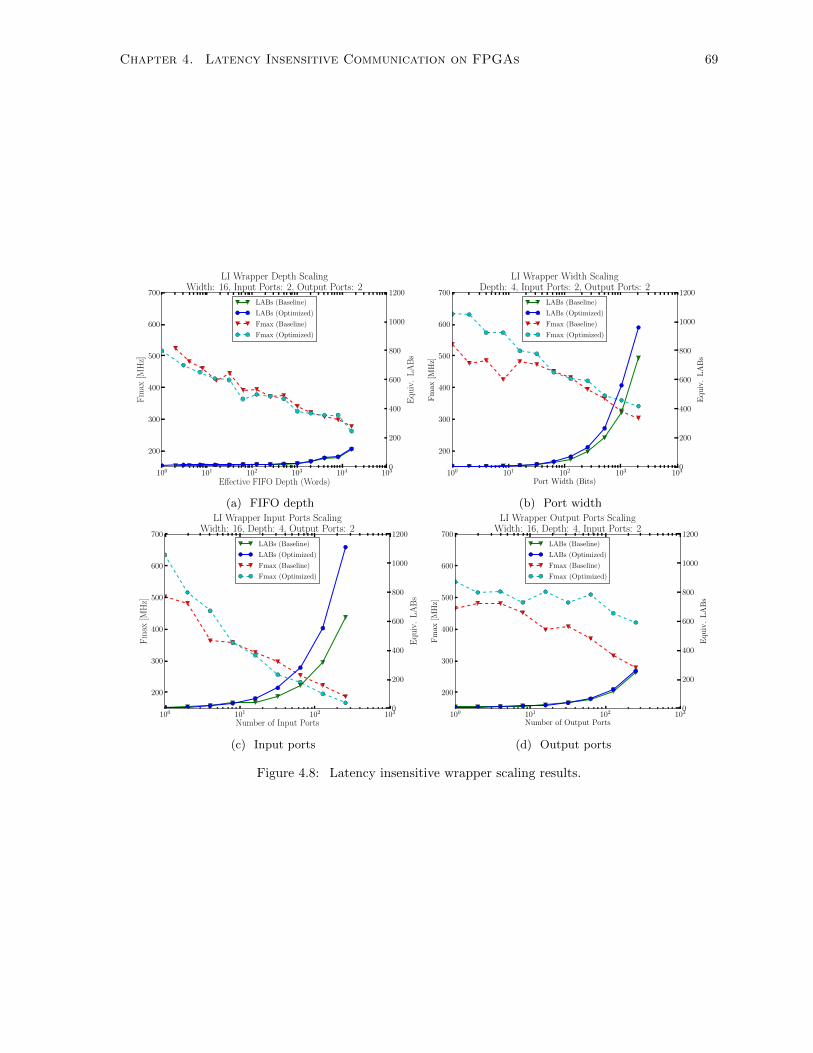
Chapter 4. Latency Insensitive Communication on FPGAs 69
100 101 102 103 104 105
Effective FIFO Depth (Words)
200
300
400
500
600
700
Fm
ax[M
Hz]
LABs (Baseline)
LABs (Optimized)
Fmax (Baseline)
Fmax (Optimized)
0
200
400
600
800
1000
1200
Equ
iv.
LA
Bs
LI Wrapper Depth ScalingWidth: 16, Input Ports: 2, Output Ports: 2
(a) FIFO depth
100 101 102 103 104
Port Width (Bits)
200
300
400
500
600
700
Fm
ax[M
Hz]
LABs (Baseline)
LABs (Optimized)
Fmax (Baseline)
Fmax (Optimized)
0
200
400
600
800
1000
1200
Equiv
.LA
Bs
LI Wrapper Width ScalingDepth: 4, Input Ports: 2, Output Ports: 2
(b) Port width
100 101 102 103
Number of Input Ports
200
300
400
500
600
700
Fm
ax[M
Hz]
LABs (Baseline)
LABs (Optimized)
Fmax (Baseline)
Fmax (Optimized)
0
200
400
600
800
1000
1200
Equ
iv.
LA
Bs
LI Wrapper Input Ports ScalingWidth: 16, Depth: 4, Output Ports: 2
(c) Input ports
100 101 102 103
Number of Output Ports
200
300
400
500
600
700
Fm
ax[M
Hz]
LABs (Baseline)
LABs (Optimized)
Fmax (Baseline)
Fmax (Optimized)
0
200
400
600
800
1000
1200
Equiv
.LA
Bs
LI Wrapper Output Ports ScalingWidth: 16, Depth: 4, Input Ports: 2
(d) Output ports
Figure 4.8: Latency insensitive wrapper scaling results.

Chapter 4. Latency Insensitive Communication on FPGAs 70
of increasing FIFO depth may be beneficial for some latency insensitive optimization schemes, which
increase FIFO depth to improve system throughput [46]. The frequency overhead of increasing FIFO
depth is moderate, as frequency remains above 300 MHz until a depth of 16K words.
Second, increasing the width of ports (Figure 4.8b) or increasing the number of input ports (Figure 4.8c)
are both fairly expensive, in terms of area and frequency overhead. However it is interesting to contrast
their relative costs. Increasing port width results in a lower area overhead than increasing the number
of input ports for the same number of overall module input bits. This is perhaps not surprising, since
increasing the port width improves the amortization of the FIFO logic, and does not introduce additional
control logic (while adding input ports does). The results are similar from a frequency perspective, with
scaling input ports more expensive than scaling port widths. The wrappers have no problem operating
above 300 MHz (using only two ports) for port widths up to 2048 bits. In contrast, this speed is only
possible if fewer than 32 ports (160 bits total) are used. Therefore, a good design recommendation is to
group input ports into a smaller number of wide ports whenever possible.
Finally, increasing the number of output ports (Figure 4.8d) is less costly, since it adds only a small
amount of control logic to handle back-pressure and valid signals. It is however, important to note
from a system perspective that each output port has an associated FIFO at the downstream input port.
Similarly to the area overhead, the frequency overhead of increasing output ports is low, with 300 MHz
operation possible with up to 256 output ports.
4.3.4 Latency Insensitive Design Overhead
One of the challenges when designing an LI system is determining the level of granularity at which to
implement latency insensitive communication. To get the most flexibility, a fine level of granularity may
be desired, but this could come at an unacceptably large area overhead.
To provide some guidance, we developed a coarse estimate of the area overhead associated with
latency insensitive communication for various module sizes by combining the results of Section 4.3.3 with
Rent’s rule, which relates I/O requirements to module size.
Rent’s rule [113], stated as:
P = KNR (4.1)
is an empirically observed relation between the average number of blocks in a module (N) and its
average number of externally connecting pins (P ), where K is the average number of pins per block
and R is the design dependant Rent parameter. The Rent parameter captures the complexity of the
interconnections between modules. A Rent parameter of 0.0 corresponds to a linear chain of modules,
such as the FIR design presented in Section 4.3.1. A Rent parameter of 1.0 corresponds to a clique where
all modules communicate with each other. Typical circuits have Rent parameters ranging from 0.45 to
0.75 [113, 114, 115].
It was found for the Titan23 benchmark set (Chapter 3) that K was 32.2 for Stratix IV LABs.
Assuming the number of pins predicted by Rent’s rule split evenly between inputs and outputs, that each
port is 64 bits wide, and FIFO depths of 4 are used, it is possible to estimate the area overhead of a
module’s latency insensitive wrapper based on the data from Section 4.3.3.
The area overhead of LI communication compared to module size is shown in Figure 4.9 for various
Rent parameter values. It is clear that modules with low to moderate Rent parameters are amenable
to the creation of area-efficient latency insensitive systems. Circuits with good communication locality

Chapter 4. Latency Insensitive Communication on FPGAs 71
103 104 105 106 107 108 109
Module Size (LEs)
0
5
10
15
20
25
30
Per
centa
geA
rea
Ove
rhea
d
LI Wrapper Area Overhead
R = 0.00
R = 0.50
R = 0.60
R = 0.65
R = 0.70
R = 0.75
Figure 4.9: Estimated latency insensitive module area overhead for various rent parameters, assumingequal numbers of input/output pins, 64-bit wide ports and FIFO depths of 4 words.
(0.5 ≤ R ≤ 0.6) can achieve low area overhead (<10%) when wrapping modules ranging in size from 50K
to 300K LEs. Circuits with moderate communication locality (0.6 < R ≤ 0.7) can achieve moderate
area overhead (<20%) when wrapping modules from 160K to 700K LEs in size. Circuits with poor
communication locality (R > 0.7) are problematic, and will likely result in latency insensitive systems
with high area overhead.
Consider the design scenario for a 4 million Logic Element (LE) FPGA, where the designer is willing
to accept a 20% area overhead. Using Figure 4.9 we can estimate the granularity needed to achieve this
based on the design’s rent parameter. For a rent parameter of 0.5, the designer can produce a fine-grained
latency insensitive system with 307 modules each roughly 13K LEs in size. For a rent parameter of
0.6, the designer can produce a somewhat coarser grained system with 71 modules each of roughly 56K
LEs. It is important to note that the relatively small module sizes for rent parameters ≤ 0.6 means that
communication with-in each module is relatively local and can still occur at high speed (c.f. 40K LEs in
Figure 2.10). As a result it is primarily global communication (whose communication speed is not scaling
as shown in Figure 2.10) that is captured by the LI part of the system. For a rent parameter of 0.7, the
designer can produce a coarse-grained system of 5 modules each containing approximately 700K LEs. In
this scenario, even though a higher rent parameter results in a coarser system, LID remains beneficial
since it still captures long distance global communication.
4.4 Conclusions
In conclusion, a quantitative analysis of the impact of latency insensitive design methodologies on FPGAs
has been presented. We have shown that system level interconnect speeds are not scaling, while local
interconnect speeds continue to improve. This mismatch, along with increasing design sizes, make LI
techniques attractive to simplify timing closure, since they allow pipelining decisions to be made late in
Chapter 4. Latency Insensitive Communication on FPGAs 72
the design cycle; possibly even by new physical CAD tools. An improved LI wrapper that addresses some
of the frequency limitations of conventional LI wrappers was presented, and was used to evaluate the area
and frequency overheads of LID. On an example system the area and frequency overheads were found
to be only 9% and 8% respectively, with the frequency overhead reducible with further pipelining. The
pipelining efficiency of LID was also compared to conventional non-LI pipelining and found to have an
overhead of 14-17%. Finally, a more general exploration of the scalability of LI wrappers was conducted,
and used to provide guidelines to designers regarding the level of granularity at which latency insensitive
communication should be implemented to maintain reasonable area overheads.
While this work shows that the frequency and area overhead of LI systems can be manageable,
it remains untenable for some classes of designs, such as those with poorly localized communication
(R > 0.7) and those unwilling to accept a 14-17% reduction in pipelining efficiency. Previous work on
statically scheduled LI systems [44] helps address this, but does so by removing much of the flexibility at
late stages of the CAD flow that LID promises.
Another approach to improve the overhead of LI systems would be to improve architectural support
for key features of LI systems. This could include improving support for low cost FIFOs supporting ‘new
data’ behaviour, and supporting fine-grained clock gating or fast clock enables.
Chapter 5
Floorplanning for Heterogeneous
FPGAs
“Civilization advances by extending the number of important operations we can
perform without thinking.”
— Alfred North Whitehead
5.1 Introduction
As outlined in Chapter 1, floorplanning enables a divide-and-conquer approach to the physical implemen-
tation of large systems by decoupling them spatially. This can be viewed as complementary to the LID
approach presented in Chapter 4 which decouples partitions from their external timing requirements.
In this chapter we present a new FPGA floorplanning tool, Hetris (Heterogeneous Region Imple-
mentation System), and investigate different aspects of floorplanning including:
• Some limitations of conventional ‘flat’ compilation methodologies and how floorplanning can offer
improvements,
• How to efficiently perform automated FPGA floorplanning,
• The structure of the FPGA floorplanning solution space and how it relates to the underlying
architecture,
• How realistic heterogeneous benchmark designs can be automatically partitioned,
• What impact floorplanning has on metrics such as required FPGA device size,
• How floorplanning performs in high resource utilization scenarios and how Hetris compares to
commercial tools.
5.2 Limitations of Flat Compilation
In the conventional FPGA CAD flow (Section 2.1.2), the physical compilation is performed in a ‘flat’
manner — where the original design hierarchy (i.e. nested modules in the original HDL) is flattened
into a single level. This has historically been done to give the physical tools full, global visibility of the
design in the hope that it will result in better optimization results. However, given the heuristic and
73

Chapter 5. Floorplanning for Heterogeneous FPGAs 74
(a) 49 Finite Impulse Response (FIR) filter cascade,with each filter given a unique colour.
(b) The critical paths of the five most critical FIR filterinstances highlighted.
Figure 5.1: Quartus II flat implementation of the 49 FIR filter cascade design.
non-optimal nature of real-world CAD tools they may get stuck in local minima. To a designer it appears
that tool has made poor decisions during the implementation process, and it may be clear to them what
can be done to improve the result.
To illustrate this, consider the cascaded FIR filter design initially presented in Section 4.3.1. The
implementation produced by Quartus II is shown in Figure 5.1a, with each FIR filter instance highlighted
in a different colour. Given that each FIR filter is largely independent (only connected to the preceding
and following filters) one would expect each filter to be well localized. While this is true in many cases,
it is clear that the flat compilation process also results in significant smearing between instances. In
particular, the five most timing critical instances, shown in Figure 5.1b are stretched out significantly,
limiting the achievable clock period.
In scenarios like this the designer’s intuition that each instance should be independent can be used
to improve the result. Manually floorplanning a 42 filter version of the FIR filter cascade, shown in
Figure 5.2, improved the achievable operating frequency from 375.38 MHz to 417.38 MHz (+11.2%).
Floorplanning (performed manually) was also found to improve frequency by Capalija and Abdelrahman
[49]. Commercial FPGA vendors [116, 117, 118] also indicate that manual floorplanning can help address
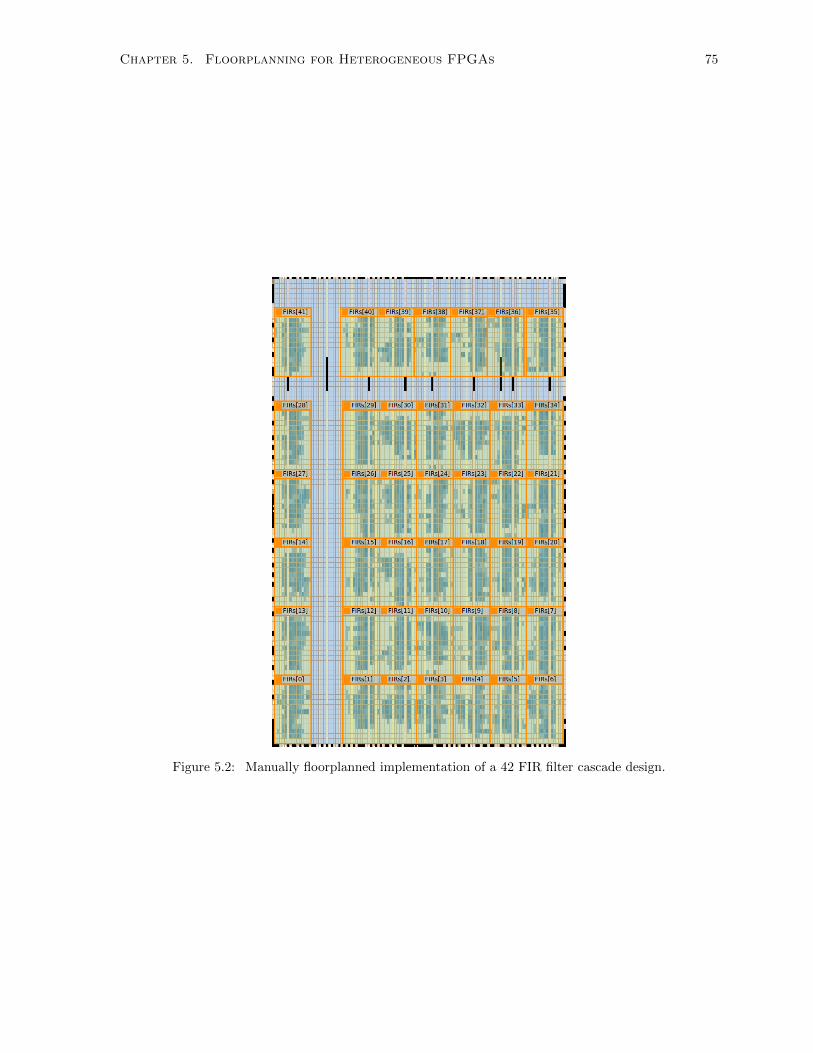
Chapter 5. Floorplanning for Heterogeneous FPGAs 75
Figure 5.2: Manually floorplanned implementation of a 42 FIR filter cascade design.

Chapter 5. Floorplanning for Heterogeneous FPGAs 76
FPGAArchitecture
Netlist
Partitioner
Partitions
Packer
ResourceRequirements
Floorplanner
Floorplan
Figure 5.3: FPGA floorplanning flow.
timing closure issues.
While floorplanning can clearly improve frequency in the cases described above, this may not always
be the case. In some scenarios the floorplanning restrictions (or poor quality floorplans/partitions) can
prevent useful optimizations from occurring across partition boundaries.
Given the time-consuming nature of manual FPGA floorplanning it is important to automate this
process. This will result in higher quality floorplans and simplify adoption by end users.
5.3 Floorplanning Flow
The design flow we used for floorplanning is shown in Figure 5.3. Initially, a flat technology mapped
netlist is produced by logic synthesis. The netlist is then partitioned, either by an automated tool or by
the user1. Once partitioned, the netlist is packed into clusters while ensuring the partition constraints
are satisfied (i.e. each cluster contains elements from only a single partition). Packing is performed
before floorplanning so that accurate resource requirements for each partition can be obtained2. The
floorplanning tool takes as input a description of the target FPGA architecture, as well as the netlist
connectivity, netlist partitions and partition resource requirements. It then attempts to find a valid
floorplan, and reports a solution if found.
1Another possible floorplanning design flow (not considered in this work) performs partitioning along the design hierarchybefore logic synthesis.
2The complex legality requirements of modern FPGA architectures makes it difficult and error prone to predict therequired resources from only the input netlist.
Chapter 5. Floorplanning for Heterogeneous FPGAs 77
5.4 Automated Floorplanning Tool
Our floorplanning tool, Hetris, builds upon Cheng and Wong’s work [56]. It uses simulated annealing
as the optimization algorithm and slicing trees to represent the relative positions of partitions in the
floorplan.
5.5 Coordinate System and Rectilinear Shapes
The coordinate system used in the floorplanner is shown in Figure 5.4. Each functional block is given an
integer x and y coordinate starting from the lower left hand corner of the device. Each resource type
consists of a rectangle width and height (both 1 in the case of a LB). Each resource type also has a
base-point or resource origin located at its lower left corner. For instance, the labelled DSP block in
Figure 5.4 is located (has its resource origin) at coordinate (4, 0).
We can then define the Resource Origin Bounding Box (ROBB) of a region as the bounding box
of all resource origins contained within the region. A ROBB is an approximate bounding box, since it
may appear to slice through resource types with dimensions greater than 1. The Exact Bounding Box
(EBB) is the precise refinement of the ROBB which accounts for resources with dimensions greater than
1. Figure 5.4 illustrates the ROBB and EBB for an example region.
For most calculations in Hetris only the ROBB is considered. This saves the computational effort of
calculating the EBB and ensures resources are allocated to only a single region at a time, since resources
are allocated to a region only if their resource origin is within the ROBB. It also helps to reduce wasted
resources by allowing region boundaries to be rectilinear based on the shapes of resources located along
the boundary. The result is similar to what is produced by Cheng and Wong’s post-processing compaction
step [56]. While it saves the computation required to perform compaction, the amount of ‘compaction’
this technique enables is limited to the maximum dimension of the largest resource type in the targeted
architecture.
5.6 Algorithmic Improvements
One of the key operations in any floorplanner is converting from an abstract floorplan representation
(such as slicing trees) to a concrete floorplan with precise locations and dimensions. As the baseline
algorithm, we use Cheng and Wong’s slicing tree evaluation algorithm to generate IRLs for the root of a
specific slicing tree. Since there may be multiple realizations of the slicing tree, the realization with the
smallest area is returned to the annealer as the floorplan associated with the slicing tree.
5.6.1 Slicing Tree IRL Evaluation as Dynamic Programming
Although not originally presented as such, Cheng and Wong’s IRL-based slicing tree evaluation algorithm
can be re-formulated as a case of dynamic programming. We can then exploit this knowledge to further
optimize its running time.
Like prototypical divide-and-conquer algorithms (e.g. quicksort) a dynamic programming problem
recursively divides the original problem into subproblems which are then solved independently and
recombined to form the final solution. However, for dynamic programming to apply two additional
characteristics must hold [77]:
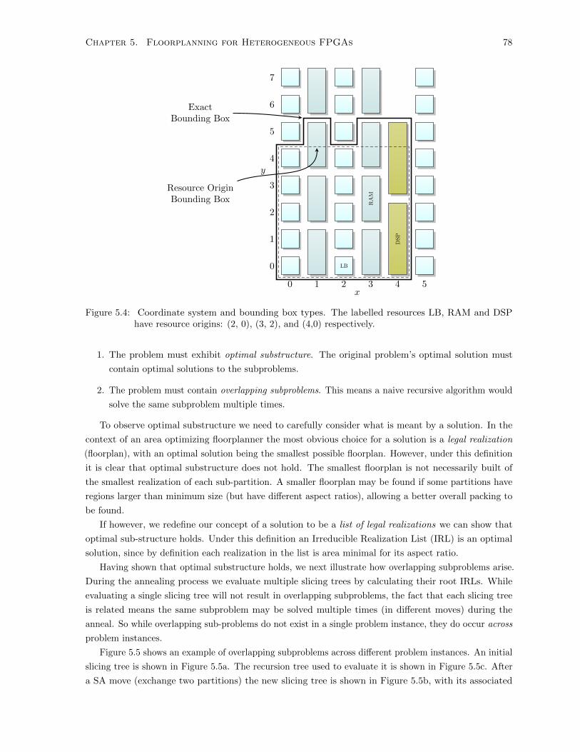
Chapter 5. Floorplanning for Heterogeneous FPGAs 78
0 1 2 3 4 5x
0
1
2
3
4
5
6
7
y
LB
RA
M
DS
P
Resource OriginBounding Box
ExactBounding Box
Figure 5.4: Coordinate system and bounding box types. The labelled resources LB, RAM and DSPhave resource origins: (2, 0), (3, 2), and (4,0) respectively.
1. The problem must exhibit optimal substructure. The original problem’s optimal solution must
contain optimal solutions to the subproblems.
2. The problem must contain overlapping subproblems. This means a naive recursive algorithm would
solve the same subproblem multiple times.
To observe optimal substructure we need to carefully consider what is meant by a solution. In the
context of an area optimizing floorplanner the most obvious choice for a solution is a legal realization
(floorplan), with an optimal solution being the smallest possible floorplan. However, under this definition
it is clear that optimal substructure does not hold. The smallest floorplan is not necessarily built of
the smallest realization of each sub-partition. A smaller floorplan may be found if some partitions have
regions larger than minimum size (but have different aspect ratios), allowing a better overall packing to
be found.
If however, we redefine our concept of a solution to be a list of legal realizations we can show that
optimal sub-structure holds. Under this definition an Irreducible Realization List (IRL) is an optimal
solution, since by definition each realization in the list is area minimal for its aspect ratio.
Having shown that optimal substructure holds, we next illustrate how overlapping subproblems arise.
During the annealing process we evaluate multiple slicing trees by calculating their root IRLs. While
evaluating a single slicing tree will not result in overlapping subproblems, the fact that each slicing tree
is related means the same subproblem may be solved multiple times (in different moves) during the
anneal. So while overlapping sub-problems do not exist in a single problem instance, they do occur across
problem instances.
Figure 5.5 shows an example of overlapping subproblems across different problem instances. An initial
slicing tree is shown in Figure 5.5a. The recursion tree used to evaluate it is shown in Figure 5.5c. After
a SA move (exchange two partitions) the new slicing tree is shown in Figure 5.5b, with its associated

Chapter 5. Floorplanning for Heterogeneous FPGAs 79
evaluation recursion tree in Figure 5.5d. Comparing the two recursion trees, it is clear that the Lb(0,0)
(highlighted) subtree is common to both — an overlapping subproblem.
Now that IRL evaluation is recognized as being suitable for dynamic programming we can exploit
these characteristics by introducing optimizations to reduce the run-time of the evaluation process.
There are two basic approaches to solving a problem by dynamic programming. The first is the
bottom-up approach which calculates all base sub-problems and then combines them to find the optimal
solution. The second is the recursive (top-down) approach. With the top-down approach the first time a
sub-problem is encountered it is ‘memoized’ by saving the result in a table. When the same sub-problem
is encountered again its result is fetched from the table rather than being recalculated. These two
methods result in the same asymptotic complexity, but the bottom-up approach typically outperforms the
top-down approach by avoiding the overheads of recursion and maintaining the table [77]. However the
top-down approach can outperform the bottom-up, if only a subset of subproblems need to be evaluated
[77].
5.6.2 IRL Memoization
The first optimization we propose is to memoize IRLs (subproblems) across SA moves. This avoids
re-calculating IRLs multiple times during the anneal3. In order to store and later look-up a memoized
subproblem a unique key identifying it must be created. Hetris uses the reverse polish notation encoding
of the associated sub-tree and the coordinates of its left-most leaf as the memoization key.
The effectiveness of this optimization depends on how often subproblems would otherwise be re-
calculated. Figure 5.6 shows the number of requests for each unique IRL over the entire annealing
process on a simple benchmark. Many IRLs are calculated multiple times, indicating that there are many
opportunities for memorization to be useful.
One potential concern about memoizing IRLs is the memory required. In Hetris, rather than
pre-allocating space for all possible IRLs (which makes a traditional Look-Up Table prohibitive), the
look-up is implemented as a dynamically sized cache using a Least Recently Used (LRU) eviction policy.
Using a cache enables a space-time trade-off. A smaller cache limits memory usage, but will capture fewer
IRLs, causing more time to be spent re-calculating them. By default the cache size is left unbounded.
This ensures that all IRLs remain memoized throughout the anneal but remains more memory efficient
than pre-allocating space, since space is only used for IRLs explored during the anneal: a small subset of
the full solution space.
5.6.3 Lazy IRL Calculation
In Cheng and Wong’s work they pre-calculate IRLs for every basic partition (leaf node in the slicing
tree) at every unique location in the FPGA before the anneal begins, which requires O(wphpWmaxHmax),
where wp and hp are the dimensions of the basic pattern while Wmax and Hmax are the maximum allowed
dimensions of a realization.
Since SA samples only a small part of the solution space, pre-calculating IRLs for every partition at
every location is unnecessary. Instead we can extend the memoization procedure to calculate the IRLs of
leaf nodes only as they are required. This ‘lazy calculation’ of leaf node IRLs avoids calculating IRLs
3One of Cheng and Wong’s performance optimizations was to pre-calculate all of the IRLs for leaf nodes. This iseffectively memoizing only at the leaf nodes of the recursion tree.
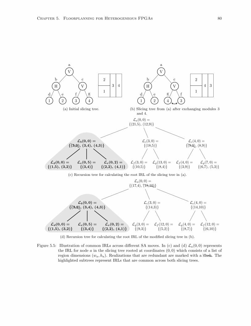
Chapter 5. Floorplanning for Heterogeneous FPGAs 80
V
V
43
H
21
a
b c
d e f g1
2
3 4
(a) Initial slicing tree.
V
V
34
H
21
a
b c
d e fg1
2
34
(b) Slicing tree from (a) after exchanging modules 3and 4.
La(0, 0) ={(21,5), (12,9)}
Lc(4, 0) ={HHH(9,9), (8,9)}
Lg(7, 0) ={(6,7), (5,3)}
Lf (4, 0) ={(3,9)}
Lc(3, 0) ={(18,5)}
Lg(13, 0) ={(8,4)}
Lf (3, 0) ={(10,5)}
Lb(0,0) ={HHH(3,9), (3,4), (4,3)}
Le(0,2) ={(2,2), (4,1)}
Le(0,5) ={(3,4)}
Ld(0,0) ={(1,5), (3,2)}
(c) Recursion tree for calculating the root IRL of the slicing tree in (a).
La(0, 0) ={(17,4), XXXX(18,10)}
Lc(4, 0) ={(14,10)}
Lf (12, 0) ={(6,10)}
Lg(4, 0) ={(8,7)}
Lc(3, 0) ={(14,3)}
Lf (12, 0) ={(5,2)}
Lg(3, 0) ={(9,3)}
Lb(0,0) ={HHH(3,9), (3,4), (4,3)}
Le(0,2) ={(2,2), (4,1)}
Le(0,5) ={(3,4)}
Ld(0,0) ={(1,5), (3,2)}
(d) Recursion tree for calculating the root IRL of the modified slicing tree in (b).
Figure 5.5: Illustration of common IRLs across different SA moves. In (c) and (d) La(0, 0) representsthe IRL for node a in the slicing tree rooted at coordinates (0, 0) which consists of a list ofregion dimensions (wa, ha). Realizations that are redundant are marked with a XXXslash. Thehighlighted subtrees represent IRLs that are common across both slicing trees.

Chapter 5. Floorplanning for Heterogeneous FPGAs 81
Figure 5.6: IRL recalculation statistics on a simple benchmark
that would never be used. This is particularly relevant for modern FPGA devices which are not tile-able4
(see Section 2.8.1)
5.6.4 Device Resource Vector Calculation
An important operation in the floorplanner is the calculation of resource vectors for a given rectangular
region on the device. RVs are used extensively during the calculation of leaf IRLs to ensure that the
resources required by a partition are satisfied.
The naive approach to calculate a resource vector for a given rectangular region is to enumerate the
block types contained within the region. This would take O(wh) time, where w and h are the region’s
width and height respectively. While this may be reasonable for small regions, it becomes prohibitively
expensive for larger regions.
Instead, for every location on the device, we pre-calculate the resource vector for the rectangle based
at the origin and extending to that location and store it in a look-up table5. This requires O(WH)
memory (where W and H are the dimensions of the device).
It is then possible to calculate the RV of any rectangular region in O(1) time according to Algorithm 4.
An example is shown in Figure 5.7. This provides fast resource vector calculation while the memory
requirements scale linearly with the size (area) of the device.
4In this situation wp = W and hp = H so the resulting complexity would be O(W 2H2) — which is prohibitivelyexpensive for large devices.
5This is similar to pre-calculating the integral of a function up to each point.

Chapter 5. Floorplanning for Heterogeneous FPGAs 82
0 1 2 3 4 5x
0
1
2
3
4
5
6
7
y
LB
RA
M
DS
P
RequestedRegion
LeftRegion
BottomRegion
CommonRegion
φtotal = (14, 8, 2)φleft = (7, 4, 0)
φbottom = (4, 2, 1)φcommon = (2, 1, 0)
Figure 5.7: Example resource vector calculation, where each φ = (nLB , nRAM , nDSP ). The resourcevector for the requested region is φ = (5, 3, 1).
Algorithm 4 Rectangular RV Query.
Require: (xmin, ymin, xmax, ymax) the coordinates of the querying rectangle, rv lookup the pre-calculated RV look-up table
1: function GetRV(xmin, ymin, xmax, ymax, rv lookup)2: φtotal ← rv lookup[xmax][ymax] . Total RV from origin to xmax, ymax3: φleft ← rv lookup[xmin][ymax] . Left of the requested region4: φbottom ← rv lookup[xmax][ymin] . Below the requested region5: φcommon ← rv lookup[xmin][ymin] . Common to left and bottom6: return φtotal − φleft − φbottom + φcommon

Chapter 5. Floorplanning for Heterogeneous FPGAs 83
5.6.5 Algorithmic Improvements Evaluation
To evaluate the presented algorithmic improvements, we evaluated the performance of Hetris by
selectively enabling the memoization and lazy evaluation optimizations. The results shown in Table 5.1
illustrate the effectiveness of these optimizations. Overall, the optimizations result in an average 15.6×speed-up. On a per-benchmark basis the best speed-ups (up to 31.3×) are obtained on the smaller
benchmarks, while on larger benchmarks which have more external nets the speed-up drops (minimum
7.2×). This difference can be explained by the two dominant components of the annealer run-time: IRL
calculation and wirelength evaluation.
Figure 5.8 illustrates the differences between the des90 and gsm switch benchmarks, which achieve
the largest and smallest speed-ups respectively. On the smaller des90 benchmark overall run-time without
lazy IRL calculation (Figure 5.8a) is dominated by IRL calculation, as there are relatively few external
nets. On the larger gsm switch benchmark the large number of external nets makes wirelength evaluation
a more significant component of total run-time (Figure 5.8c) limiting the potential speed-up when lazy
IRL calculation is used. Lazy IRL calculation yields a larger improvement in run-time (5.42× vs. 2.27×)
compared to IRL memoization. The quality of results for all 4 algorithmic variations in Table 5.1 are
identical since they calculate identical IRLs.
BenchmarkExternal
Net Count
LazyMemoize All
(min)
LazyMemoize Leaves
(min)
ExhaustiveMemoize All
(min)
ExhaustiveMemoize Leaves
(min)
gsm switch 241,048 22.06 (7.15×) 44.45 (3.55×) 67.59 (2.34×) 157.86 (1.00×)sparcT2 core 182,698 17.86 (8.66×) 48.47 (3.19×) 61.69 (2.51×) 154.65 (1.00×)
mes noc 115,606 66.78 (9.27×) 212.36 (2.91×) 251.83 (2.46×) 619.05 (1.00×)minres 112,234 7.63 (12.12×) 19.82 (4.66×) 41.59 (2.22×) 92.39 (1.00×)dart 108,408 13.77 (11.30×) 40.87 (3.81×) 65.55 (2.37×) 155.53 (1.00×)
SLAM spheric 82,370 7.00 (14.91×) 22.26 (4.69×) 45.44 (2.30×) 104.33 (1.00×)denoise 76,377 16.10 (13.31×) 52.80 (4.06×) 82.86 (2.59×) 214.34 (1.00×)
cholesky bdti 74,921 7.42 (15.26×) 21.94 (5.16×) 47.14 (2.40×) 113.23 (1.00×)segmentation 73,086 11.04 (14.74×) 37.53 (4.34×) 73.35 (2.22×) 162.80 (1.00×)sparcT1 core 70,874 5.36 (19.14×) 16.20 (6.34×) 47.53 (2.16×) 102.61 (1.00×)bitonic mesh 61,110 3.73 (18.80×) 6.28 (11.17×) 33.88 (2.07×) 70.10 (1.00×)
openCV 60,981 4.34 (18.94×) 10.44 (7.88×) 40.56 (2.03×) 82.26 (1.00×)stap qrd 51,755 17.15 (10.49×) 58.47 (3.08×) 69.02 (2.61×) 179.87 (1.00×)
des90 37,368 2.38 (31.29×) 5.02 (14.84×) 36.50 (2.04×) 74.55 (1.00×)stereo vision 35,103 2.34 (29.78×) 6.73 (10.34×) 33.50 (2.08×) 69.64 (1.00×)cholesky mc 32,408 3.14 (31.02×) 13.69 (7.11×) 41.85 (2.33×) 97.33 (1.00×)
neuron 31,365 2.71 (26.91×) 11.28 (6.46×) 32.96 (2.21×) 72.83 (1.00×)
GEOMEAN 72,148 7.89 (15.62×) 22.74 (5.42×) 54.01 (2.28×) 123.28 (1.00×)
Table 5.1: Run-time of lazy leaf IRL calculation and IRL memoization optimizations on 17 of the Titanbenchmarks. Each benchmark was partitioned by Metis into 32 parts and floorplanned on atile-able Stratix IV-like architecture. Values shown in brackets are speed-ups compared to thealgorithm presented by Cheng and Wong [56], which corresponds to the ‘Exhaustive MemoizeLeaves’ column.

Chapter 5. Floorplanning for Heterogeneous FPGAs 84
72.6%
21.8%
5.6%
Slicing Tree
Cost Function
Other
(a) Smaller des90 benchmark without lazy IRLcalculation.
16.4%
73.6%
10.0%
Slicing Tree
Cost Function
Other
(b) Smaller des90 benchmark with lazy IRL calculation.
51.9% 44.4%
3.7%
Slicing Tree
Cost Function
Other
(c) Larger gsm switch benchmark without lazy IRLcalculation.
20.5%
74.9%
4.6%
Slicing Tree
Cost Function
Other
(d) Larger gsm switch benchmark with lazy IRLcalculation.
Figure 5.8: Impact of lazy IRL calculation on relative time spent during slicing trees evaluation, annealercost function evaluation and other operations (e.g. file parsing and IO). In all cases IRLmemoization is enabled. The cost function calculation is always dominated by the Half-Perimeter Wirelength (HPWL) evaluation.

Chapter 5. Floorplanning for Heterogeneous FPGAs 85
(a) Resource-oblivious floorplan (b) Resource-aware floorplan
Figure 5.9: Resource-oblivious and Resource-aware Floorplans, for the same slicing tree, when thebenchmark and targeted architecture are closely matched. In this case the resource-obliviousfloorplan is largely similar to the resource-aware floorplan.
5.7 Annealer
While Section 5.6 described some of the fundamental enhancements to the internal floorplan realization
algorithms, an equally important component is the outer annealing algorithm.
5.7.1 Initial Solution
All SA algorithms require some initial solution. In most of the previous work, the initial solution is
created by solving a simplified version of the full heterogeneous floorplanning problem. For instance
Cheng and Wong perform initial floorplanning while ignoring the heterogeneous resource requirements.
Their motivation is that by finding a sufficiently good initial solution while ignoring heterogeneity, they
can start their heterogeneous resource-aware annealer at a lower temperature to reduce run-time.
After re-implementing their approach we found that the initial resource-oblivious floorplanner is faster
(∼ 1.5× on the des90 benchmark with 32 partitions) than the resource-aware floorplanner. However,
in contrast to Cheng and Wong we found that the initial solution was no better than starting from an
arbitrary initial solution, and as a result the additional run-time spent generating an initial solution was
better spent in the primary resource-aware annealer.
We believe the reason behind this differing conclusion is related to the benchmarks and architectures
being evaluated. We are using real FPGA circuits to evaluate the floorplanner (see Section 5.11), while
Cheng and Wong used ‘adapted’ ASIC floorplanning benchmarks. In adapting the ASIC benchmarks
Cheng and Wong assume a distribution of heterogeneous resources closely matching the underlying FPGA
architecture. This close match between the benchmarks and architecture means their resource-oblivious
initial floorplanning still produces a useful initial solution — that is, the resource-oblivious floorplan of
the initial floorplanning slicing tree is similar to the resource-aware realization (c.f. Figures 5.9a and 5.9b).
However, assuming such a close match between architecture and benchmark is unrealistic. Most FPGA
designs are much more unbalanced in two ways: between different partitions in a benchmark, and between

Chapter 5. Floorplanning for Heterogeneous FPGAs 86
(a) Resource-oblivious floorplan (b) Resource-aware floorplan (illegal)
Figure 5.10: Resource-oblivious and resource-aware floorplans, for the same slicing tree and benchmarkin Figure 5.9. However in this case, there is a realistic mismatch between the benchmark andtarget architecture. The resource-oblivious floorplan bears little resemblance to the resource-aware floorplan. The resource-aware floorplan consumes ∼ 2.5× more area and requiresmuch wider regions which make the floorplan illegal. As a result the resource-obliviousfloorplan is of little use as an initial solution.
the partitions and the target architecture. As a result, on realistic benchmarks the difference between
resource-oblivious and resource-aware floorplanning can be quite significant — reducing the effectiveness
of any initial floorplanning that neglects the heterogeneous nature of the FPGA floorplanning problem
(c.f. Figures 5.10a and 5.10b). As a result Hetris by default constructs an arbitrary initial solution
and directly begins resource-aware floorplanning instead of attempting any initial resource-oblivious
floorplanning.
5.7.2 Initial Temperature Calculation
The initial temperature is calculated before the start of the main annealing process by performing O(N43 )
randomized moves and evaluating the resulting costs. Based on the average cost of the evaluated moves,
the average positive delta cost (δ+) is calculated. The initial temperature is then calculated according to
the metropolis criteria to achieve a user defined target acceptance rate for uphill moves (λ+target):
Tinit = −δ+/ln(λ+target). (5.1)
Setting λ+target to a value in the range 0.4-0.8 is usually sufficient to ensure a high enough initial
temperature to broadly explore the solution space. To reduce run-time lower values can be used, which
focuses Hetris on fine tuning the initial solution, rather than searching for the best possible solution.
5.7.3 Annealing Schedule
The annealing schedule is based on the adaptive annealing schedule used by VPR [93]. Under this
annealing schedule the acceptance rate (Definition 5) is calculated on-line as the anneal progresses. The
temperature is then adjusted to try and keep the acceptance rate close to 0.44 where the annealer is
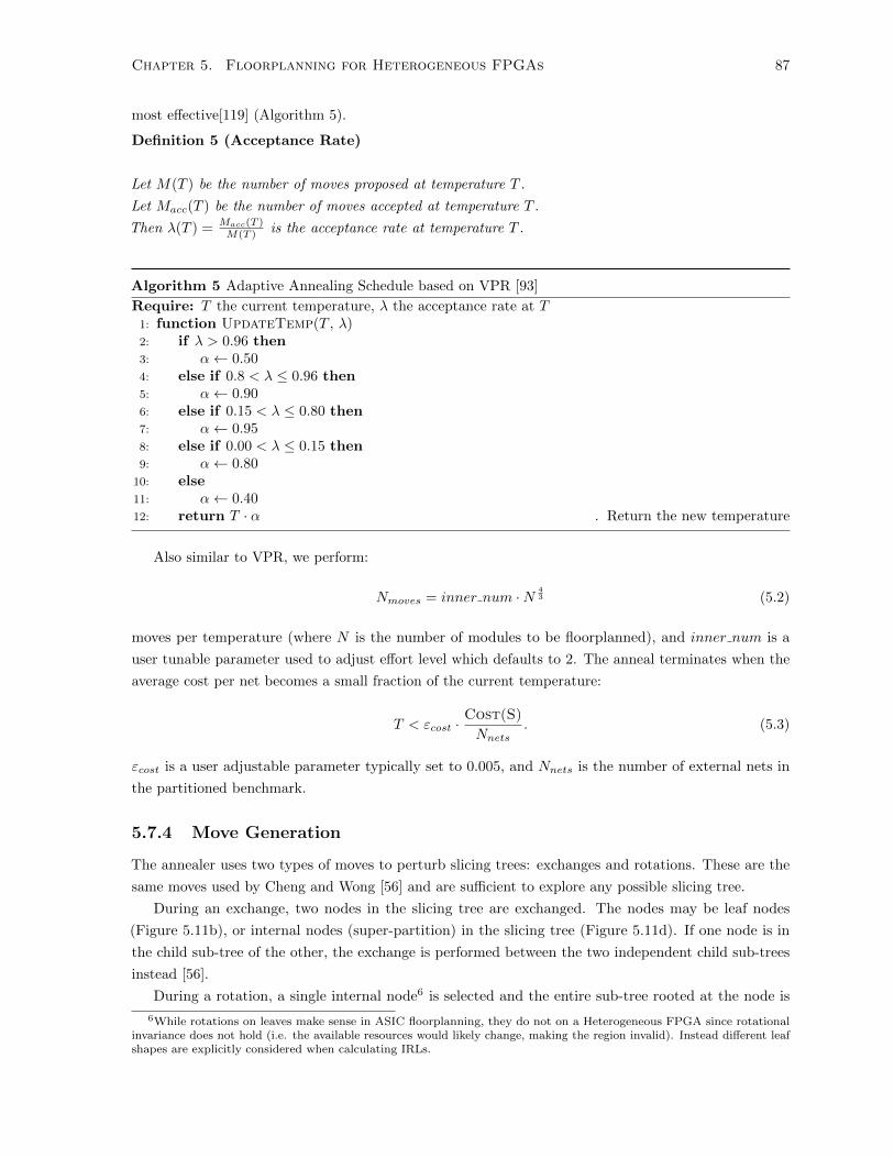
Chapter 5. Floorplanning for Heterogeneous FPGAs 87
most effective[119] (Algorithm 5).
Definition 5 (Acceptance Rate)
Let M(T ) be the number of moves proposed at temperature T .
Let Macc(T ) be the number of moves accepted at temperature T .
Then λ(T ) = Macc(T )M(T ) is the acceptance rate at temperature T .
Algorithm 5 Adaptive Annealing Schedule based on VPR [93]
Require: T the current temperature, λ the acceptance rate at T1: function UpdateTemp(T , λ)2: if λ > 0.96 then3: α← 0.504: else if 0.8 < λ ≤ 0.96 then5: α← 0.906: else if 0.15 < λ ≤ 0.80 then7: α← 0.958: else if 0.00 < λ ≤ 0.15 then9: α← 0.80
10: else11: α← 0.4012: return T · α . Return the new temperature
Also similar to VPR, we perform:
Nmoves = inner num ·N 43 (5.2)
moves per temperature (where N is the number of modules to be floorplanned), and inner num is a
user tunable parameter used to adjust effort level which defaults to 2. The anneal terminates when the
average cost per net becomes a small fraction of the current temperature:
T < εcost ·Cost(S)
Nnets. (5.3)
εcost is a user adjustable parameter typically set to 0.005, and Nnets is the number of external nets in
the partitioned benchmark.
5.7.4 Move Generation
The annealer uses two types of moves to perturb slicing trees: exchanges and rotations. These are the
same moves used by Cheng and Wong [56] and are sufficient to explore any possible slicing tree.
During an exchange, two nodes in the slicing tree are exchanged. The nodes may be leaf nodes
(Figure 5.11b), or internal nodes (super-partition) in the slicing tree (Figure 5.11d). If one node is in
the child sub-tree of the other, the exchange is performed between the two independent child sub-trees
instead [56].
During a rotation, a single internal node6 is selected and the entire sub-tree rooted at the node is
6While rotations on leaves make sense in ASIC floorplanning, they do not on a Heterogeneous FPGA since rotationalinvariance does not hold (i.e. the available resources would likely change, making the region invalid). Instead different leafshapes are explicitly considered when calculating IRLs.

Chapter 5. Floorplanning for Heterogeneous FPGAs 88
V
H
43
H
21
a
b c
d e f g1
23
4
(a) Initial Slicing Tree and Floorplan.
V
H
42
H
31
a
b c
d ef g1 2
34
(b) After exchanging modules 2 and 3 in (a)
V
V
42
H
31
a
b c
d ef g1 2
3
4
(c) After rotating clockwise at c in (b).
V
3H
V
42
1
a
b
cd
e
f
g
1
23
4
(d) After exchanging module 3 and the super-partitionrooted at c in (c).
Figure 5.11: Illustration of slicing tree moves.
rotated (Figure 5.11c).
5.8 Cost Functions
An important aspect of any annealer are the cost functions used to evaluate candidate solutions. We
define the base cost functions as those used to evaluate the quality of a solution, while cost penalties
(Section 5.10.1) penalize illegality to guide the annealer to a valid solution.
5.8.1 Base Cost Function
The base cost of a solution S is calculated according to Equation (5.4).
BaseCost(S) = Afac ·Area(S)
Areanorm+Bfac ·
ExtWL(S)
ExtWLnorm+ Cfac ·
IntWL(S)
IntWLnorm(5.4)
Where Area, ExtWL, and IntWL are calculated based on the current solution (S) as described below.
The various factors (e.g. Afac) are user adjustable weights used to control the relative importance of the
different cost components.
5.8.2 Cost Function Normalization
One of the challenges when dealing with a multi-objective optimization problem is handling the different
dimensionality of the cost components (e.g. area has dimension length2, while wirelength has dimension

Chapter 5. Floorplanning for Heterogeneous FPGAs 89
length1), and their widely varying magnitudes. To compensate for this, each cost component is normalized
by dividing by the respective normalization factor (e.g. Areanorm). The normalization factors are set to
the average value of each cost component observed while making the randomized moves to determine the
initial temperature (Section 5.7.2). This ensures each normalized quantity (e.g. Area(S)Areanorm
) is dimensionless
and takes on a value of 1.0 on a typical solution.
5.8.3 Area Cost
The area of a floorplan is calculated as the ROBB of all its constituent modules. The floorplan ROBB is
determined as part of the IRL calculation process, and corresponds to the realization of the root module
in the slicing tree. It is also important to note that the ROBB is precisely accurate along a device’s
fixed-outline (since blocks do not straddle the outline) — so it will never inaccurately report an illegal
solution as legal.
5.8.4 External Wirelength Cost
The external wirelength cost is approximated by the HPWL metric, shown in Equation (5.5) where Nnet
is the number of nets between modules, and bbwidth(i) and bbheight(i) are the width and height of net i’s
bounding box respectively.
ExtWL =
Nnet∑i=1
bbwidth(i) + bbheight(i) (5.5)
Since pin locations are not yet known, it is assumed that all nets connect to the centre of a module7.
The process of evaluating the HPWL takes O(kNnet) time where Nnet is the number of nets affected
by a move, and k is the maximum net fanout. Despite being linear in the number of nets, the HPWL
calculation is one of the most significant components of the floorplanner’s run-time.
VPR faces a similar issue during placement, and uses an incremental approach to avoid the O(k)
re-calculation of a net’s bounding box in most cases. While this incremental approach was shown to offer
a significant (∼ 5×) speed-up in VPR [16] it is actually slower than the brute force recomputation when
used in Hetris. This somewhat surprising result is caused by the significantly more disruptive nature of
moves during floorplanning compared to the moves used during placement.
As shown in Figure 5.12 most moves during floorplanning affect a large number of nets (e.g. only
18% of moves affect fewer than 97% of nets). Compared to placement (where individual functional blocks
are moved), the partitions moved during floorplanning are larger and more strongly interconnected.
Furthermore, the shape and position of each partition’s associated region is dependant upon the other
partitions — a move affecting a small part of the slicing tree may cause all regions to change location
and shape. As a result, most floorplanning moves affect a large number of modules and nets. The result
is the extra book-keeping overhead required for incremental HPWL calculation out-weighs the relatively
few times it avoids recalculating a net’s bounding box.
7This is a first order approximation to the final pin locations. Better estimates of pin locations [120] would likely improvethe final (post-routing) Quality of Result (QoR). However such approaches are not investigated here, and are left for futurework.

Chapter 5. Floorplanning for Heterogeneous FPGAs 90
0.0 0.2 0.4 0.6 0.8 1.0Fraction of Total Moves
0.0
0.2
0.4
0.6
0.8
1.0
Fra
ctio
nA
ffec
ted
Partition Regions
Nets
Figure 5.12: Fraction of nets and partitions affected by moves on the radar20 benchmark. Approximately7.2% of moves have no effect on nets or regions since the moves transition between equivalentslicing trees.
5.8.5 Internal Wirelength Cost
As noted in Section 2.6, extreme aspect ratios may be detrimental to the final internal wirelength of a
module. While the extreme cases are handled by limiting the maximum allowable aspect ratios, it is also
useful to allow the annealer to optimize aspect ratios so they remain near 1.
Directly estimating the internal wirelength would be computationally prohibitive, so like Cheng and
Wong we adopt the aspect ratio based metric defined in Equation (5.6).
IntWL =
N∑i=1
w2i + h2i (5.6)
5.9 Solution Space Structure
Given the space of all possible solutions, we can view the annealer as traversing a cost surface defined by
the cost function. The surface which we are trying to optimize (ignoring legality) is defined by the base
cost function (Equation (5.4)).
FPGA Architecture and Solution Space Structure
Figure 5.13 illustrates the solution space, allowing us to make several interesting observations.
Firstly, solutions are only found at specific discrete locations8, creating ‘families’ of solutions along
curves of constant width. This clustering is an artifact of the targeted FPGA architecture. In this
case, the architecture is a conventional column-based architecture where each column contains a specific
resource type. As a result only some floorplan widths are capable of supporting the required resource
types.
8This highlights the discrete nature of the FPGA floorplanning problem. A similar plot generated by an ASIC toolwould likely not exhibit such a clustering of solutions.
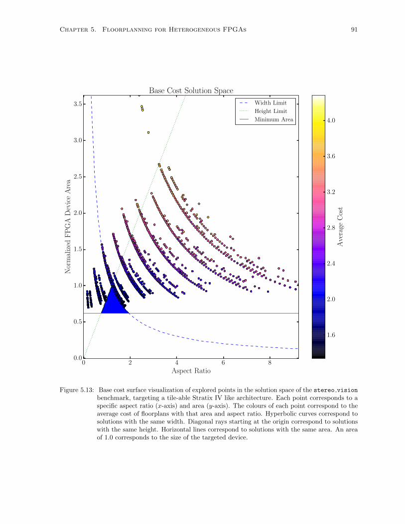
Chapter 5. Floorplanning for Heterogeneous FPGAs 91
0 2 4 6 8
Aspect Ratio
0.0
0.5
1.0
1.5
2.0
2.5
3.0
3.5
Nor
mal
ized
FP
GA
Dev
ice
Are
a
Base Cost Solution Space
Width Limit
Height Limit
Minimum Area
1.6
2.0
2.4
2.8
3.2
3.6
4.0
Ave
rage
Cos
t
Figure 5.13: Base cost surface visualization of explored points in the solution space of the stereo vision
benchmark, targeting a tile-able Stratix IV like architecture. Each point corresponds to aspecific aspect ratio (x-axis) and area (y-axis). The colours of each point correspond to theaverage cost of floorplans with that area and aspect ratio. Hyperbolic curves correspond tosolutions with the same width. Diagonal rays starting at the origin correspond to solutionswith the same height. Horizontal lines correspond to solutions with the same area. An areaof 1.0 corresponds to the size of the targeted device.
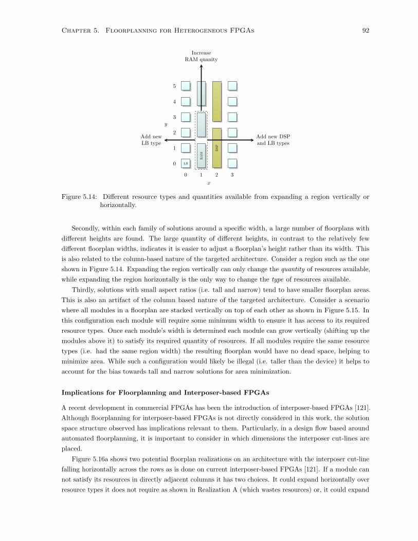
Chapter 5. Floorplanning for Heterogeneous FPGAs 92
0 1 2 3
x
0
1
2
3
4
5
y
LB
RA
M
DSP
Add newLB type
IncreaseRAM quanity
Add new DSPand LB types
Figure 5.14: Different resource types and quantities available from expanding a region vertically orhorizontally.
Secondly, within each family of solutions around a specific width, a large number of floorplans with
different heights are found. The large quantity of different heights, in contrast to the relatively few
different floorplan widths, indicates it is easier to adjust a floorplan’s height rather than its width. This
is also related to the column-based nature of the targeted architecture. Consider a region such as the one
shown in Figure 5.14. Expanding the region vertically can only change the quantity of resources available,
while expanding the region horizontally is the only way to change the type of resources available.
Thirdly, solutions with small aspect ratios (i.e. tall and narrow) tend to have smaller floorplan areas.
This is also an artifact of the column based nature of the targeted architecture. Consider a scenario
where all modules in a floorplan are stacked vertically on top of each other as shown in Figure 5.15. In
this configuration each module will require some minimum width to ensure it has access to its required
resource types. Once each module’s width is determined each module can grow vertically (shifting up the
modules above it) to satisfy its required quantity of resources. If all modules require the same resource
types (i.e. had the same region width) the resulting floorplan would have no dead space, helping to
minimize area. While such a configuration would likely be illegal (i.e. taller than the device) it helps to
account for the bias towards tall and narrow solutions for area minimization.
Implications for Floorplanning and Interposer-based FPGAs
A recent development in commercial FPGAs has been the introduction of interposer-based FPGAs [121].
Although floorplanning for interposer-based FPGAs is not directly considered in this work, the solution
space structure observed has implications relevant to them. Particularly, in a design flow based around
automated floorplanning, it is important to consider in which dimensions the interposer cut-lines are
placed.
Figure 5.16a shows two potential floorplan realizations on an architecture with the interposer cut-line
falling horizontally across the rows as is done on current interposer-based FPGAs [121]. If a module can
not satisfy its resources in directly adjacent columns it has two choices. It could expand horizontally over
resource types it does not require as shown in Realization A (which wastes resources) or, it could expand

Chapter 5. Floorplanning for Heterogeneous FPGAs 93
0 1 2 3 4 5x
0
1
2
3
4
5
6
7
8
9
y
LBR
AM
DSP
Region A
Region B
Region C
(a) Module widths to satisfy resource types, but ignor-ing required quantities.
0 1 2 3 4 5x
0
1
2
3
4
5
6
7
8
9
y
LB
RA
M
DSP
Region A
Region B
Region C
FlooprlanBounding Box
(b) Floorplan satisfying resource quantities by onlyexpanding vertically.
Figure 5.15: A potential configuration for vertically stacked modules, φA = (4, 2, 1), φB = (4, 2, 0),φC = (2, 0, 0).
vertically along the column and cross the interposer cut-line as shown with Realization B (which imposes
a delay penalty and reduces routing flexibility [122]). Clearly neither of these options is desirable.
If however, the architecture placed the interposer cut-lines in the vertical direction between columns
(Figure 5.16b), a better result is obtained. With this architecture, the realization can expand vertically
along the column (which wastes no resources) and does not cross the interposer (Realization B). As a
result, from a floorplanning perspective (targeting a column-based FPGA) a vertically sliced interposer
architecture is preferable to a horizontally sliced one, since it helps to minimize wasted resources and the
number of interposer crossings within a floorplanned region. As an alternative interpretation, given the
bias towards tall and narrow floorplans in column based FPGAs, it is preferable to keep the interposer
slices with a similar (tall and narrow) aspect ratio, which is accomplished by placing the cut-lines along
the columns rather than along the rows.
Exploiting Solution Space Structure
The previous discussion indicates that the solution space has structure which it may be possible to exploit
to speed-up the search process. Consider the following:
• Relatively few families of solutions have widths that would potentially allow a member to be a legal
solution.
• It is relatively easy to find a shorter floorplan given some floorplan with an initial width and height.
• The various families of solutions could be identified early in the annealing process.
A potential approach that would exploit these characteristics would be the following:
1. Perform a fast initial (randomized) search of the solution space to identify families of solutions.
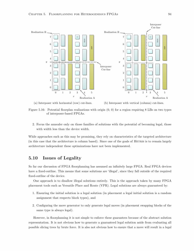
Chapter 5. Floorplanning for Heterogeneous FPGAs 94
0 1 2 3 4 5
x
0
1
2
3
4
5
6
7
y
LB
RA
M
DSP
Realization A
Realization B
InterposerCut-line
(a) Interposer with horizontal (row) cut-lines.
0 1 2 3 4 5
x
0
1
2
3
4
5
6
7
y
LB
RA
M
DSP
Realization A
Realization B
InterposerCut-line
(b) Interposer with vertical (column) cut-lines.
Figure 5.16: Potential floorplan realizations with origin (0, 0) for a region requiring 8 LBs on two typesof interposer-based FPGAs.
2. Focus the annealer only on those families of solutions with the potential of becoming legal, those
with width less than the device width.
While approaches such as this may be promising, they rely on characteristics of the targeted architecture
(in this case that the architecture is column based). Since one of the goals of Hetris is to remain largely
architecture independent these optimizations have not been implemented.
5.10 Issues of Legality
So far our discussion of FPGA floorplanning has assumed an infinitely large FPGA. Real FPGA devices
have a fixed-outline. This means that some solutions are ‘illegal’, since they fall outside of the required
fixed-outline of the device.
One approach is to disallow illegal solutions entirely. This is the approach taken by many FPGA
placement tools such as Versatile Place and Route (VPR). Legal solutions are always guaranteed by:
1. Ensuring the initial solution is a legal solution (in placement a legal initial solution is a random
assignment that respects block types), and
2. Configuring the move generator to only generate legal moves (in placement swapping blocks of the
same type is always legal).
However, in floorplanning it is not simple to enforce these guarantees because of the abstract solution
representation. It is not obvious how to generate a guaranteed legal solution aside from evaluating all
possible slicing trees by brute force. It is also not obvious how to ensure that a move will result in a legal

Chapter 5. Floorplanning for Heterogeneous FPGAs 95
solution without evaluating each move. As a result of these challenges, Hetris allows illegal solutions
during floorplanning. This also has the potential benefit of helping to prevent the annealer from becoming
stuck in local optima. It may be that escaping from local optima may only be possible by transitioning
through an illegal part of the solution space.
One of the key issues with allowing illegal solutions is how to ensure a legal solution is eventually
found. To accomplish this, a cost penalty9 is used to penalize illegal solutions. This makes legal solutions
appear more desirable (lower cost), helping direct the annealer towards them.
5.10.1 An Adaptive Approach
One of the most important considerations when designing a cost penalty is how it should be scaled
relative to other costs and how it should evolve during the annealing process. The cost penalty must
balance two competing factors: the desire to ensure a legal solution is found, and the desire to minimize
any impact on the final QoR. While an illegal final solution is useless, a legal but poor quality solution is
also undesirable.
It is also desirable for the cost penalty approach to be robust across a range of FPGA architectures
and benchmarks. One approach is to expose a large number of tuning parameters which control the cost
penalty behaviour — allowing it to be tuned for specific architectures (or benchmarks). However this
places additional burden on the tool user, as it is not obvious how any tuning parameters should be
configured. Instead we propose an adaptive cost penalty which adjusts automatically10 to the target
architecture and benchmark. This allows the tool to focus its efforts on solution quality for benchmarks
with easily found legal solutions, and on finding legal solutions for difficult benchmarks.
Cost Penalty
The extended cost function takes the form of Equation (5.7), where Pfac is the current penalty factor
(which changes through the anneal), and Illegality(S) is a measure of how illegal a particular solution
is.
Cost(S) = BaseCost(S) + Pfac ·Illegality(S)
Illegalitynorm(5.7)
The illegality value is normalized in the same manner as the base cost components (Section 5.8.2). The
value of Pfac is increased through out the annealing process depending on how successful the annealer is
at finding legal solutions.
This idea of ‘success’ is captured by a new annealing metric, the legal acceptance rate:
Definition 6 (Legal Acceptance Rate)
Let Mlegal acc(T ) be the number of accepted moves that were legal at temperature T .
Then λlegal(T ) =Mlegal acc(T )Macc(T ) is the legal acceptance rate at temperature T .
A λlegal close to 0 implies that very few legal solutions have been found, while a value near 1 implies
that nearly all accepted moves are legal. The legal acceptance rate is calculated in an on-line manner
during the annealing process.
9Analogous to barrier functions used with continuous optimization.10This is similar to the concept of self-adapting evolutionary algorithms which optimize their parameters as part of the
evolutionary process [123], and to the adaptive annealing schedule used in VPR [93].

Chapter 5. Floorplanning for Heterogeneous FPGAs 96
The value of Pfac is updated according to Equation (5.8) at the end of each temperature.
Pfac =
Pfac · P 2
fac scale λlegal(T ) ≤ 0.1 · λlegal targetPfac · Pfac scale 0.1 · λlegal target < λlegal(T ) < λlegal target
Pfac λlegal(T ) ≥ λlegal target
(5.8)
If the legal acceptance rate is below the target legal acceptance rate then Pfac increases exponentially,
otherwise it remains fixed. λlegal target is typically set close to or equal to 1.0; this ensures that the tool
will increase the cost penalty for illegality until only legal solutions are accepted.
Empirically we have found values of Pfac scale in the range 1.005 to 1.2 perform well. Small values
typically take longer to converge to legal solutions but typically result in better quality solutions. With
large values Pfac grows large so quickly it dominates all other cost components before a legal solution
is found. As a result few (if any) moves appear better than the current (illegal) solution, causing the
acceptance rate to drop and the annealing schedule to enter the rapid cooling phase.
While the initial value of Pfac defaults to 1.0 (i.e. the same as any other cost component), it can be
set to larger values (e.g. 10.0) which forces the tool to start focusing on legality earlier in the anneal.
This can reduce the amount of time required to find the initial legal solution but, like large values of
Pfac scale, runs the risk of freezing the solution in an illegal state.
One approach to capture the degree of illegality of a given solution is to calculate how much area falls
outside the fixed device outline (Equation (5.9)).
Illegality(S) =
AreaFP −AreaDEV AreaFP > AreaDEV
0 AreaFP ≤ AreaDEV(5.9)
As a result, the cost penalty is smooth (not a binary legal/illegal response). This helps to guide the
annealer by showing it that solutions with less area outside the device are closer to being legal.
Adjusting the Cooling Rate
Since it may take time for the adaptive cost penalty factor to ramp up, one of the challenges is ensuring
it becomes large enough to be effective (that is, of sufficient magnitude to influence the acceptance rate
and push the annealer towards legal solutions) at an appropriate point during the anneal. If the penalty
only becomes effective near the end of the anneal, then the annealer may become stuck in an illegal local
minima. We would therefore like for the cost penalty to become effective at a high enough temperature
that the annealer can still hill-climb efficiently and find its way to a legal solution.
One approach would be to select the initial Pfac and Pfac scale so they reached sufficient magnitude
after a fixed number of temperatures. However since the adaptive annealing schedule in Section 5.7.3
is dependant on the run-time behaviour of the annealer these values can not be calculated a priori.
Instead we accomplish our goal by augmenting the annealing schedule described in Section 5.7.3, to
additionally consider the legal acceptance rate. The new algorithm for updating the temperature is shown
in Algorithm 6. With this cooling schedule the annealer ‘stalls’ (α = 0.99)11 if the legal acceptance rate
is too small. If the legal acceptance rate is approaching the target then the original annealing schedule is
11Note that the annealer does not strictly stall — α remains less than 1.0, ensuring the temperature continues to decreaseand that the anneal will eventually terminate. However by using a value close to 1.0 the temperature decreases slowly,effectively stalling the anneal.

Chapter 5. Floorplanning for Heterogeneous FPGAs 97
Algorithm 6 Augmented Adaptive Annealing Schedule
Require: T the current temperature, λ the acceptance rate at T , λlegal the legal acceptance rate at T ,λlegal target the target legal acceptance rate
1: function UpdateTempStall(T , λ, λlegal, λlegal target)2: Tnew ← UpdateTemp(T, λ) . As in Algorithm 53: if 0.1 < λ ≤ 0.9 then . Don’t stall at the beginning or end of the anneal4: if λlegal ≤ 0.8 · λlegal target then . Only stall if reasonably far from the target rate5: α← 0.996: Tnew ← T · α7: return Tnew
used. At the beginning (λ > 0.9) and end (λ < 0.1) of the anneal the original schedule is used regardless
of the legal acceptance rate, since stalling at these points is unlikely to improve quality.
5.10.2 How To Tune A Cost Surface?
Adding an illegality term to the cost function (i.e. Equation (5.7)) transforms the shape of the cost
surface, meaning the annealer is no longer directly optimizing the base cost function12. The explored
solution space evaluated with the final cost function at the end of the anneal is shown in Figure 5.17.
The addition of the cost penalty transforms the cost surface so that it slopes much more steeply towards
legal solutions.
However, in the annealer run shown in Figure 5.17 no legal solution was found, despite exploring
a number of nearly-legal solutions. An example nearly-legal floorplan is shown in Figure 5.18a, while
a legal one is shown in Figure 5.18b. Clearly, to transform the illegal floorplan into a legal one, the
floorplan needs to be ‘squished’ to the left and expanded upwards.
To gain further insight into why so many nearly-legal (but no legal) solutions were found, it is useful
to look at the behaviour of the annealer as a function of time. Figure 5.19 plots various annealer statistics
as a function of the number of iterations (temperatures) during the same annealing run. Looking at the
acceptance rates we observe that during the initial high temperature stages of the anneal (Temperature
Number < 40) Hetris finds many solutions that are vertically legal (λvert legal), and some solutions
which are horizontally legal (λhoriz legal) but none that are legal in both dimensions. However as the cost
penalty increases the annealer abandons the horizontally legal solutions to focus almost exclusively on
vertically legal solutions. Eventually (Temperature Number ∼ 120) the illegality cost (Penalty) grows
so large that the system freezes (no moves look better than the current illegal solution), causing the
temperature to drop rapidly and terminate the anneal.
The key issue in this case is that the illegality cost penalizes both horizontal and vertical illegality the
same way. Given a horizontally illegal solution, a move that would make it horizontally legal would likely
result in a solution which is more vertically illegal than the current solution, making such a solution have
higher cost and likely not be accepted. This traps the annealer in an illegal solution. An alternative view
is, given the propensity of vertical legality to be obtained more easily, a uniform penalty often results in
horizontally illegal solutions.
12This is similar in many ways to Stochastic Tunnelling (STUN), a technique which transforms an annealer’s cost functionto help it escape local minima [124]. STUN techniques have previously been applied to FPGA placement [125]. Like STUN,our illegality penalty adaptively changes the cost surface based upon the on-line measured behaviour of the annealer. Thekey differences between STUN and our approach are the form of the transformation and purpose behind it — our approachattempts to guide the annealer towards legal solutions, rather than help it escape local minima.

Chapter 5. Floorplanning for Heterogeneous FPGAs 98
0 2 4 6 8
Aspect Ratio
0.0
0.5
1.0
1.5
2.0
2.5
3.0
3.5
Nor
mal
ized
FP
GA
Dev
ice
Are
a
Final Cost Solution Space(Combined Area Penalty)
Width Limit
Height Limit
Minimum Area
106
107
108
Ave
rage
Cos
tNearly-Legal
Figure 5.17: Cost surface visualization of the same annealer run as Figure 5.13, but evaluated usingthe cost function at the end of the anneal (including the illegality penalty). ‘Width Limit’and ‘Height Limit’ correspond to the dimensions of the targeted device. ‘Minimum Area’ isthe area required if partitions are ignored. The shaded triangular-shape denotes the regionof legal solutions. No legal solutions were found in this run. The nearly legal solutionsclustered along ‘Width Limit’ are one column wider than the device.
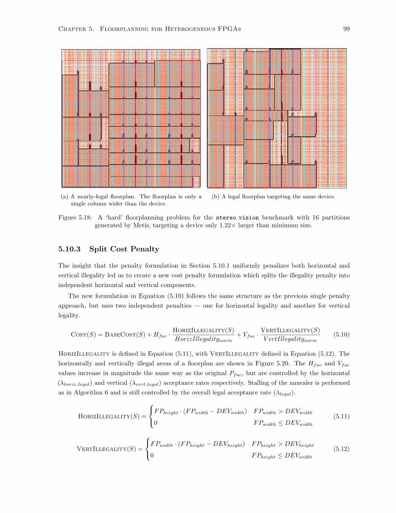
Chapter 5. Floorplanning for Heterogeneous FPGAs 99
(a) A nearly-legal floorplan. The floorplan is only asingle column wider than the device.
(b) A legal floorplan targeting the same device.
Figure 5.18: A ‘hard’ floorplanning problem for the stereo vision benchmark with 16 partitionsgenerated by Metis, targeting a device only 1.22× larger than minimum size.
5.10.3 Split Cost Penalty
The insight that the penalty formulation in Section 5.10.1 uniformly penalizes both horizontal and
vertical illegality led us to create a new cost penalty formulation which splits the illegality penalty into
independent horizontal and vertical components.
The new formulation in Equation (5.10) follows the same structure as the previous single penalty
approach, but uses two independent penalties — one for horizontal legality and another for vertical
legality.
Cost(S) = BaseCost(S) +Hfac ·HorizIllegality(S)
HorizIllegalitynorm+ Vfac ·
VertIllegality(S)
V ertIllegalitynorm(5.10)
HorizIllegality is defined in Equation (5.11), with VertIllegality defined in Equation (5.12). The
horizontally and vertically illegal areas of a floorplan are shown in Figure 5.20. The Hfac and Vfac
values increase in magnitude the same way as the original Pfac, but are controlled by the horizontal
(λhoriz legal) and vertical (λvert legal) acceptance rates respectively. Stalling of the annealer is performed
as in Algorithm 6 and is still controlled by the overall legal acceptance rate (λlegal).
HorizIllegality(S) =
FPheight · (FPwidth −DEVwidth) FPwidth > DEVwidth
0 FPwidth ≤ DEVwidth(5.11)
VertIllegality(S) =
FPwidth · (FPheight −DEVheight) FPheight > DEVheight
0 FPheight ≤ DEVwidth(5.12)

Chapter 5. Floorplanning for Heterogeneous FPGAs 100
0.2
0.4
0.6
0.8
1.0
1.2
1.4
Cos
t(Z
oom
)
Annealer Statistics
Area
ExtWL
IntWL
10−1
100
101
102
103
104
105
106
Cos
t
Area
ExtWL
IntWL
Penalty
101
102
103
104
105
106
107
108
109
Pen
alty
Fac
tor
Pfac
0.0
0.2
0.4
0.6
0.8
1.0
Acc
epta
nce
Rat
e(λ
) λ
λlegal
λvert legal
λhoriz legal
0 20 40 60 80 100 120 140 160 180
Temperature Number
10−1
100
101
102
103
Tem
per
atu
re(T
)
Penalty Dominates
Freeze Point
Horizontal LegalityAbandoned
Vertical LegalityAchieved
Figure 5.19: Single cost penalty annealer statistics as a function of time (number of temperatures) on thestereo vision benchmark. Note that Legal Acceptance Rate (λlegal) stays zero throughoutthe entire anneal. None of the explored solutions are both vertically and horizontally legal.
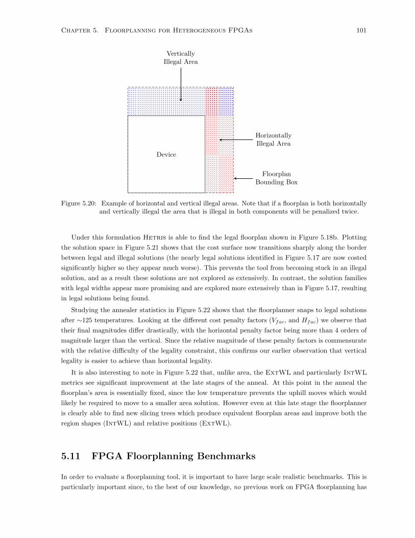
Chapter 5. Floorplanning for Heterogeneous FPGAs 101
Device
FloorplanBounding Box
HorizontallyIllegal Area
VerticallyIllegal Area
Figure 5.20: Example of horizontal and vertical illegal areas. Note that if a floorplan is both horizontallyand vertically illegal the area that is illegal in both components will be penalized twice.
Under this formulation Hetris is able to find the legal floorplan shown in Figure 5.18b. Plotting
the solution space in Figure 5.21 shows that the cost surface now transitions sharply along the border
between legal and illegal solutions (the nearly legal solutions identified in Figure 5.17 are now costed
significantly higher so they appear much worse). This prevents the tool from becoming stuck in an illegal
solution, and as a result these solutions are not explored as extensively. In contrast, the solution families
with legal widths appear more promising and are explored more extensively than in Figure 5.17, resulting
in legal solutions being found.
Studying the annealer statistics in Figure 5.22 shows that the floorplanner snaps to legal solutions
after ∼125 temperatures. Looking at the different cost penalty factors (Vfac, and Hfac) we observe that
their final magnitudes differ drastically, with the horizontal penalty factor being more than 4 orders of
magnitude larger than the vertical. Since the relative magnitude of these penalty factors is commensurate
with the relative difficulty of the legality constraint, this confirms our earlier observation that vertical
legality is easier to achieve than horizontal legality.
It is also interesting to note in Figure 5.22 that, unlike area, the ExtWL and particularly IntWL
metrics see significant improvement at the late stages of the anneal. At this point in the anneal the
floorplan’s area is essentially fixed, since the low temperature prevents the uphill moves which would
likely be required to move to a smaller area solution. However even at this late stage the floorplanner
is clearly able to find new slicing trees which produce equivalent floorplan areas and improve both the
region shapes (IntWL) and relative positions (ExtWL).
5.11 FPGA Floorplanning Benchmarks
In order to evaluate a floorplanning tool, it is important to have large scale realistic benchmarks. This is
particularly important since, to the best of our knowledge, no previous work on FPGA floorplanning has

Chapter 5. Floorplanning for Heterogeneous FPGAs 102
0 2 4 6 8
Aspect Ratio
0.0
0.5
1.0
1.5
2.0
2.5
3.0
3.5
Nor
mal
ized
FP
GA
Dev
ice
Are
a
Final Cost Solution Space(Split Horiz. and Vert. Penalty)
Width Limit
Height Limit
Minimum Area
101
102
103
104
105
106
107
Ave
rage
Cos
tNot Explored
Explored
Figure 5.21: Cost surface visualization at the end of an anneal using the split cost penalty. Thebenchmark (stereo vision) and target architecture are identical to Figures 5.13 and 5.17.

Chapter 5. Floorplanning for Heterogeneous FPGAs 103
0.20.40.60.81.01.21.41.61.82.0
Cos
t(Z
oom
)
Annealer Statistics
Area
ExtWL
IntWL
10−1
100
101
102
103
104
105
Cos
t
Area
ExtWL
IntWL
Vert. Penalty
Horiz. Penalty
101
102
103
104
105
106
107
Pen
alty
Fac
tor
Vfac
Hfac
0.0
0.2
0.4
0.6
0.8
1.0
Acc
epta
nce
Rat
e(λ
) λ
λlegal
λvert legal
λhoriz legal
0 50 100 150 200 250 300
Temperature Number
10−710−610−510−410−310−210−1
100101102103104105
Tem
per
atu
re(T
)
Late CostImprovements
Horizontal LegalityAchieved
Vertical LegalityAchieved
LegalityAchieved
Stall Begins Stall Ends
Figure 5.22: Split cost penalty annealer statistics as a function of time (number of temperatures) forthe stereo vision benchmark.
Chapter 5. Floorplanning for Heterogeneous FPGAs 104
used real FPGA benchmark designs13.
The Titan benchmarks presented in Chapter 3 are large and realistic. However, since the Titan
benchmarks were not originally designed with floorplanning in mind (they assumed a traditional flat
compilation flow) they provide no design partitions. As a result design partitions must be generated for
each benchmark.
In ASIC design flows where floorplanning is more commonly used, the design is often manually
partitioned to reflect the logical hierarchy of the system being designed. This maximizes the benefit of a
large team-based design approach where each group can work (largely independently) on their own logical
portion of the design, which is eventually integrated into the complete physical design. An alternative
approach is to partition the design based on its physical structure. This is typically accomplished by
using an automated tool which attempts to optimize some characteristic of the partitioning such as
minimizing the amount of communication between partitions.
The choice of partitions is likely to have a significant impact on the overall result of any floorplanning
based design flow, so it is important to make ‘good’ partitioning choices. Given the design dependent
nature of logical partitioning and its time consuming (manual) nature we have focused on physical
partitioning, which can be done quickly using automated tools such as Metis and hMetis [126, 89] are
known to produce high quality partitions. Additionally Metis and hMetis allow us to easily modify the
characteristics of the partitioning such as how unbalanced partitions are, and how many partitions should
be created. We also consider the automatic design partitions produced by a commercial FPGA CAD
tool, Quartus II’s ‘Design Partition Planner’; however this tool only generates a single set of partitions
and provides no control of their characteristics14.
5.11.1 Partitioning Considerations
Automated partitioning tools typically attempt to minimize the graph (Metis) or hyper-graph (hMetis)
cut-size, the number of edges or hyper-edges with terminals in different partitions, while keeping the
different partitions ‘well balanced’. Balance constraints are defined by the ratio of a partition’s size to its
target size (partition sizetarget size ). By default the target partition size is set to perfectly balance the partitions.
We define the allowed unbalance as a percentage of target size. For instance an unbalance of 5% would
restrict the partition size to follow the inequality: 0.95 · target size ≤ partition size ≤ 1.05 · target size.The heterogeneous nature of FPGAs complicates the idea of balance between partitions since it requires
multiple types of resources to be balanced. Both tools provide the ability to allow more unbalance
between partitions which typically helps to reduce the cut-size.
While hMetis typically achieves lower cut-size since it considers hyper-edges (edges which connect to
multiple nodes, a good model for nets in a netlist) it does not support balancing multiple resource types
between partitions. This results in some partitions having a large number of a particular resource type.
If an unbalanced resource type is relatively ‘rare’ in the targeted FPGA, it can cause significant area
bloat. As a result hMetis was not investigated further.
Metis supports heterogeneous balancing constraints between partitions, but only supports simple
graphs (instead of hypergraphs) in which edges in the graph only connect to two nodes. As a result,
the input netlist must be transformed from a hypergraph into a graph. It was previously observed
13All previous work has either used synthetically generated benchmarks, or adapted ASIC floorplanning benchmarks,which as noted in Section 5.7.1 can lead to misleading results.
14We used the Design Partition Planner provided with version 12.0 of Quartus II, which does provide some options tocontrol the resulting partitioning. However modifying these settings did not change the resulting partitions.

Chapter 5. Floorplanning for Heterogeneous FPGAs 105
that using a star net model and a net weighting of 1/Net Fanout produced good partitions [127], so
this transformation was used. Several additional netlist transformations are required to improve Metis’
partitioning quality and ensure the partitions are legal, as detailed below.
Logical RAMs
Logical RAMs are typically represented as single-bit wide RAM slices. While these slices share control
signals, each is connected to unique data bits. As a result the partitioning tool has a tendency to place
different slices of a single logical ram into different partitions. This requires each partition with a slice of
the logical RAM to use at least one memory block, significantly increasing the memory block requirements
of the partitioned circuit, compared with the unpartitioned version. To avoid this issue we transform
the netlist before partitioning to collapse logical RAMs into a single node with equivalent weight (i.e.
weight equal to the number of ram slices collapsed). This ensures logical RAMs do not straddle partitions
(preventing area bloat) and that the overall balance of RAM components between partitions remains
fairly even.
Complex Packing Constraints
Some blocks in an FPGA have complex constraints that require certain netlist primitives to be packed
together. Examples of this include arithmetic carry-chains and combined DSP multipliers and accumu-
lators. Since these netlist primitives must be packed together into the same block, they can not span
partitions. To ensure the partitioner respects these legality constraints, blocks of these types are collapsed
down into a single node in a manner similar to logical RAMs.
Sparse Resources
Most FPGA circuits contain large numbers of some resource types (e.g. LUTs and FFs), but often a
small number of other resource types (e.g. I/Os and PLLs). Care must be taken when partitioning to
account for the situation when there are more partitions than there are resource types (e.g. 1 PLL and 4
partitions). In these cases, the allowable unbalance for sparse resource types must be set large enough so
the partitioner does not try to balance this unbalance-able resource.
5.11.2 Architecture-Aware Netlist Partitioning Problem
Although the previous discussion has focused on producing well balanced partitions (since this is what
Metis supports), a well balanced partitioning of resources is not necessarily the best possible partitioning
for floorplanning. While the desire for well balanced partitions is well founded (it avoids the extremely
unbalanced case which causes area bloat), what we really desire is an architecture aware resource
partitioning. That is, we seek a partitioning of an input netlist where each partition has a resource
distribution which closely matches that of the targeted FPGA architecture. This would help to minimize
the size of floorplanned regions since each partition’s resource requirements would be similar to the
targeted architecture.
Definition 7 (Normalized Resource Vector)
Let φ = (n1, n2, . . . , nk) be a resource vector (Definition 3).
Then φ = ( n1
n1+n2+···+nk, n2
n1+n2+···+nk, . . . , nk
n1+n2+···+nk) is a normalized resource vector.

Chapter 5. Floorplanning for Heterogeneous FPGAs 106
A potential formal definition of the architecture aware partitioning problem is presented in Equa-
tion (5.13). The goal of the optimization problem is to minimize some combination of total resource
mismatch (between the partitions and architecture) and the weighted cut-size. P is the set of netlist
partitions, N is the number of partitions, and G(V,E) is the hypergraph representing the input netlist —
consisting of vertices V and hyperedges E. Each hyperedge e has weight w(e). φ(pi) is the normalized
resource vector (Definition 7) of partition i, and φarch is the normalized resource vector of the targeted
FPGA architecture.
minimizeP
f(resource mismatch, cut size)
resource mismatch =
N∑i=0
|φ(pi)− φarch|
cut size =∑
e∈E|e crosses partitions
w(e)
subject to pi ∩ pj = ∅ ∀i, j ∈ N | j 6= i
N⋃i=0
pi = V
(5.13)
The constraint pi ∩ pj = ∅ ensures each partition is independent (netlist resources can only be assigned to
a single partition), while⋃Ni=0 pi = V ensures each vertex in the netlist hypergraph is assigned to some
partition.
A variant of this problem, which is useful when multiple design teams are working on different parts
of a design, is shown in Equation (5.14). This variant restricts cuts in the netlist hypergraph to follow
the logical structure of the design, which consists of M logical modules.
minimizeP
f(resource mismatch, cut size)
resource mismatch =
N∑i=0
|φ(pi)− φarch|
cut size =∑
e∈E|e crosses partitions
w(e)
subject to pi ∩ pj = ∅ ∀i, j ∈ N | j 6= i
N⋃i=0
pi = V
mi ⊂ pj j ∈ N, ∀i ∈M
(5.14)
The constraint mi ⊂ pj ensures that each logical module mi in the design is completely contained in (i.e.
is only part of) some partition pj .
To the best of our knowledge there are no tools that attempt to address either variant of the
architecture aware partitioning problem.

Chapter 5. Floorplanning for Heterogeneous FPGAs 107
5.12 Evaluation Methodology
This section describes the methodology used to evaluate Hetris and empirically investigate some of the
characteristics of the floorplanning problem.
5.12.1 Quality of Result Metrics and Comparisons
While ideally we would like to evaluate the quality of Hetris by assessing its overall impact on the CAD
flow (i.e. post-routing results) this falls beyond the scope of this work. Instead, like nearly all previous
works on floorplanning we focus on QoR metrics which can be easily measured directly after floorplanning
is complete. The two primary metrics are the area of the resulting floorplan and its estimated wirelength.
It would be desirable to compare Hetris with previous work which has addressed the FPGA
floorplanning problem, but this is not possible for several reasons. Firstly, there is no consistent set of
benchmarks or target architectures used for evaluating FPGA floorplanning algorithms. In particular,
the benchmarks used by Cheng and Wong were never publicly released and are no longer available [128].
Secondly, to the best of our knowledge none of the previous work has publicly released their floorplanning
tools in either source or executable form. This makes it impossible to directly compare to previous work.
While the algorithms presented in many of the previous works are important contributions in-and-of-
themselves, the heuristic nature of all these approaches makes the actual implementation a key component
of their work. Failure to present implementations also makes it difficult and time consuming to build
upon others previous work, since much of the basic infrastructure must be re-built. To help address
these issues, we plan to publicly release the source code for Hetris and also the full set of floorplanning
benchmarks (including partitions) and target architectures used.
5.12.2 Design Flow
Figure 5.23 illustrates the design flow used to evaluate Hetris. The initial benchmark netlist is partitioned
using either Metis or Quartus II. VPR then packs the netlist into the functional blocks of the target
architecture while respecting the partitioning requirements. The resultant packing is used to determine
the resource requirements (in terms of functional blocks) of each partition. Finally, Hetris floorplans
the partitioned netlist onto the specified FPGA architecture.
5.12.3 Target Architecture, Benchmarks and Tool Settings
We target a tile-able version of the Stratix IV architecture presented in Chapter 3. To make the
architecture tile-able, I/Os were placed in columns rather than around the device perimeter, and column
spacings were adjusted to follow a repeating pattern15. The basic tile of this architecture consists of 336
unique locations (wp = 42, hp = 8). This is larger than the 100 location (wp = 25, hp = 4) basic tile used
by Cheng and Wong to model a Xilinx XC3S5000 FPGA.
The size of the targeted FPGA is determined by the resource requirements of each benchmark as
shown in Equation (5.15).
TargetSize = β ·MinimumSize (5.15)
15Note that Hetris can support non-tile able architectures. A non-tileable architecture can be viewed as consisting of asingle large tile. We use a tile-able architecture here to remain similar to previous work.

Chapter 5. Floorplanning for Heterogeneous FPGAs 108
VTR FPGAArchitecture Description BLIF Netlist
Partitioner(Metis/Quartus II)
Partitions
Packer(VPR)
ResourceRequirements
Floorplanner(Hetris)
Floorplan
Figure 5.23: Floorplanning flow used to evaluate Hetris.
The MinimumSize is determined by finding the smallest number of basic tiles which satisfy the total
resource requirements of the partitioned netlist. More formally, the MinimumSize is determined by
finding the smallest region R with width k ·wp, and height c ·hp (k, c ∈ Z+) such that φ(R) ≥∑Ni=0 φ(pi).
We then floorplan 17 of the 23 Titan benchmarks (Chapter 3) listed in Table 5.2a. The 6 largest
Titan benchmarks were not considered because of the substantial packing run-time required by VPR.
The key settings used when evaluating Hetris are listed in Table 5.2b. Also listed (where applicable)
are the corresponding symbols and associated equation numbers.
A large value was chosen for auto device scale to ensure that large FPGA devices were used and
hence legality issues did not distract the annealer from minimizing metrics such as floorplan area. An
irl dimension limit of 3.0 indicates that the maximum realization dimension is 3.0× the corresponding
device dimension. This value often needs to be greater than 1.0 (i.e. allow floorplans with dimensions
larger than the device) to ensure some, possibly illegal, initial solutions are found. If the value is too
small, no solutions may be found during initial temperature calculation.
5.13 Hetris Quality/Run-time Trade-offs
In this section, we investigate the impact of the different tuning parameters on the quality and run-time
characteristics of Hetris using the methodology and baseline settings described in Section 5.12. We
perform several different experiments:
• Section 5.13.1 investigates the impact of limiting the allowed aspect ratios of floorplan regions,
Chapter 5. Floorplanning for Heterogeneous FPGAs 109
Benchmarks
mes nocgsm switch
denoisesparcT2 corecholesky bdti
minresstap qrdopenCV
dartbitonic meshsegmentationSLAM spheric
des90cholesky mcstereo visionsparcT1 core
neuron
(a) 17 Titan benchmarks used forevaluation.
Tool Setting Symbol(s) Associated Equation Value
auto device scale β 5.15 6.0irl dimension limit – – 3.0irl aspect limit γmax, 1/γmin 2.5 5.0
target uphill acc rate λ+target 5.1 0.8inner num inner num 5.2 2.0
epsilon cost εcost 5.3 0.005invalid fp cost fac Pfac scale 5.8 1.10
(b) Settings for Hetris.
Table 5.2: Default evaluation configuration.
• Section 5.13.2 investigates the impact of adjusting the maximum allowed dimensions of floorplan
regions, and
• Section 5.13.3 investigates the impact of adjusting Hetris’s effort level.
5.13.1 Impact of Aspect Ratio Limits
Tables 5.3a and 5.3b illustrate the impact on run-time and floorplan area respectively, of varying the aspect
ratio limits applied to all leaf-nodes in the slicing tree. The most flexible case (γmax = 0) corresponds to
no aspect ratio limit.
The smallest area is achieved with no aspect ratio constraints, but this comes at the cost of increased
run-time since longer IRLs must be calculated. Forcing a square shape on all leaf modules (γmax = 1)
Benchmarkγmax = 0
(Unbounded)γmax = 1(Square)
γmax = 3 γmax = 6
mes noc 17.40 57.55 102.02gsm switch 54.86 (1.00×) 25.77 (0.47×) 32.72 (0.60×) 30.84 (0.56×)
denoise 64.78 (1.00×) 10.56 (0.16×) 18.35 (0.28×) 24.63 (0.38×)sparcT2 core 161.39 (1.00×) 13.74 (0.09×) 18.72 (0.12×) 21.41 (0.13×)cholesky bdti 13.47 (1.00×) 6.70 (0.50×) 10.65 (0.79×) 11.18 (0.83×)
minres 12.54 (1.00×) 11.01 (0.88×) 11.81 (0.94×) 13.41 (1.07×)stap qrd 46.52 (1.00×) 7.19 (0.15×) 20.84 (0.45×) 25.73 (0.55×)openCV 8.30 (1.00×) 8.11 (0.98×) 6.31 (0.76×) 8.42 (1.01×)
dart 47.13 (1.00×) 8.07 (0.17×) 12.96 (0.28×) 17.02 (0.36×)bitonic mesh 6.50 (1.00×) 10.21 (1.57×) 8.84 (1.36×) 5.07 (0.78×)segmentation 38.77 (1.00×) 6.00 (0.15×) 10.32 (0.27×) 15.50 (0.40×)SLAM spheric 14.80 (1.00×) 5.21 (0.35×) 8.59 (0.58×) 10.44 (0.71×)
des90 3.65 (1.00×) 4.26 (1.17×) 2.95 (0.81×) 3.08 (0.84×)cholesky mc 6.42 (1.00×) 2.70 (0.42×) 3.58 (0.56×) 4.60 (0.72×)stereo vision 5.02 (1.00×) 3.54 (0.71×) 3.41 (0.68×) 3.69 (0.74×)sparcT1 core 13.26 (1.00×) 3.61 (0.27×) 5.89 (0.44×) 7.25 (0.55×)
neuron 6.06 (1.00×) 3.81 (0.63×) 4.49 (0.74×) 5.47 (0.90×)
GEOMEAN 17.26 (1.00×) 7.23 (0.40×) 10.02 (0.52×) 11.75 (0.59×)
(a) Hetris run-time in minutes.
Benchmarkγmax = 0
(Unbounded)γmax = 1(Square)
γmax = 3 γmax = 6
mes noc 36,288 31,360 31,600gsm switch 26,448 (1.00×) 37,696 (1.43×) 28,296 (1.07×) 28,296 (1.07×)
denoise 24,384 (1.00×) 34,272 (1.41×) 26,416 (1.08×) 25,400 (1.04×)sparcT2 core 17,848 (1.00×) 22,680 (1.27×) 19,304 (1.08×) 18,600 (1.04×)cholesky bdti 14,224 (1.00×) 23,876 (1.68×) 16,320 (1.15×) 14,280 (1.00×)
minres 27,432 (1.00×) 43,200 (1.57×) 29,464 (1.07×) 26,416 (0.96×)stap qrd 20,320 (1.00×) 29,412 (1.45×) 21,632 (1.06×) 21,336 (1.05×)openCV 26,752 (1.00×) 52,328 (1.96×) 31,228 (1.17×) 32,512 (1.22×)
dart 9,120 (1.00×) 14,400 (1.58×) 9,520 (1.04×) 9,520 (1.04×)bitonic mesh 28,296 (1.00×) 41,912 (1.48×) 29,920 (1.06×) 28,296 (1.00×)segmentation 14,240 (1.00×) 34,476 (2.42×) 16,376 (1.15×) 17,576 (1.23×)SLAM spheric 10,160 (1.00×) 26,416 (2.60×) 12,920 (1.27×) 11,684 (1.15×)
des90 15,664 (1.00×) 36,504 (2.33×) 15,640 (1.00×) 16,376 (1.05×)cholesky mc 10,200 (1.00×) 29,412 (2.88×) 13,172 (1.29×) 11,220 (1.10×)stereo vision 10,880 (1.00×) 50,600 (4.65×) 13,940 (1.28×) 12,240 (1.13×)sparcT1 core 5,160 (1.00×) 35,448 (6.87×) 6,235 (1.21×) 5,934 (1.15×)
neuron 9,504 (1.00×) 18,720 (1.97×) 12,168 (1.28×) 10,880 (1.14×)
GEOMEAN 15,158 (1.00×) 31,727 (2.08×) 17,869 (1.14×) 17,071 (1.08×)
(b) Floorplan area in grid locations achieved by Hetris
Table 5.3: Impact of different IRL aspect ratio restrictions. Results are for 32 partitions with themaximum IRL dimension limited to 6× the device dimensions.
Chapter 5. Floorplanning for Heterogeneous FPGAs 110
Benchmark Dimension Limit=1 Dimension Limit=3 Dimension Limit=6
mes nocgsm switch 2,217.72 (1.00×) 2,647.24 (1.19×) 3,291.81 (1.48×)
denoise 3,688.85 (1.00×) 6,037.27 (1.64×) 3,886.57 (1.05×)sparcT2 core 1,766.81 (1.00×) 4,474.70 (2.53×) 9,683.51 (5.48×)cholesky bdti 520.38 (1.00×) 822.23 (1.58×) 808.30 (1.55×)
minres 389.14 (1.00×) 654.90 (1.68×) 752.22 (1.93×)stap qrd 2,077.78 (1.00×) 5,516.87 (2.66×) 2,790.92 (1.34×)openCV 214.92 (1.00×) 378.03 (1.76×) 498.02 (2.32×)
dart 1,249.58 (1.00×) 2,634.03 (2.11×) 2,827.57 (2.26×)bitonic mesh 267.57 (1.00×) 339.47 (1.27×) 390.24 (1.46×)segmentation 1,274.68 (1.00×) 1,741.96 (1.37×) 2,326.02 (1.82×)SLAM spheric 463.38 (1.00×) 666.28 (1.44×) 887.99 (1.92×)
des90 146.71 (1.00×) 248.46 (1.69×) 218.73 (1.49×)cholesky mc 146.11 (1.00×) 349.27 (2.39×) 385.29 (2.64×)stereo vision 155.63 (1.00×) 221.97 (1.43×) 301.25 (1.94×)sparcT1 core 352.48 (1.00×) 770.20 (2.19×) 795.45 (2.26×)
neuron 128.93 (1.00×) 247.04 (1.92×) 363.85 (2.82×)
GEOMEAN 530.32 (1.00×) 928.56 (1.75×) 1,035.72 (1.95×)
(a) Hetris run-time in minutes.
Benchmark Dimension Limit=1 Dimension Limit=3 Dimension Limit=6
mes nocgsm switch 27,984 (1.00×) 26,208 (0.94×) 26,448 (0.95×)
denoise 24,384 (1.00×) 24,768 (1.02×) 24,384 (1.00×)sparcT2 core 17,664 (1.00×) 17,000 (0.96×) 17,848 (1.01×)cholesky bdti 14,872 (1.00×) 13,600 (0.91×) 14,224 (0.96×)
minres 25,440 (1.00×) 26,416 (1.04×) 27,432 (1.08×)stap qrd 20,176 (1.00×) 20,320 (1.01×) 20,320 (1.01×)openCV 28,392 (1.00×) 26,400 (0.93×) 26,752 (0.94×)
dart 9,432 (1.00×) 9,360 (0.99×) 9,120 (0.97×)bitonic mesh 26,200 (1.00×) 28,296 (1.08×) 28,296 (1.08×)segmentation 14,240 (1.00×) 14,240 (1.00×) 14,240 (1.00×)SLAM spheric 10,200 (1.00×) 10,200 (1.00×) 10,160 (1.00×)
des90 17,272 (1.00×) 17,816 (1.03×) 15,664 (0.91×)cholesky mc 10,880 (1.00×) 12,168 (1.12×) 10,200 (0.94×)stereo vision 10,200 (1.00×) 10,880 (1.07×) 10,880 (1.07×)sparcT1 core 5,600 (1.00×) 5,160 (0.92×) 5,160 (0.92×)
neuron 10,716 (1.00×) 9,348 (0.87×) 9,504 (0.89×)
GEOMEAN 15,472 (1.00×) 15,330 (0.99×) 15,158 (0.98×)
(b) Floorplan area achieved by Hetris
Table 5.4: Impact of different IRL dimension limits. Results are for 32 partitions with no aspect ratiolimit.
achieves a 2.4× speed-up, but also results in a poorly packed floorplan requiring over 2.0× more area
than in the unbounded case. Allowing more permissive aspect ratios quickly gains back much of the area
overhead at the cost of additional run-time, for γmax = 6 we achieve a speed-up of nearly 1.5× compared
to the unconstrained case, while requiring only 8% additional area. While no aspect ratio limits result in
the best quality (smallest) floorplans, results of similar quality with reduced run-time can be achieved by
restricting the allowed aspect ratios to moderate values.
Interestingly the run-time benefit and area overhead can vary largely between benchmarks, particularly
at restrictive aspect ratio limits such as γmax = 1. Benchmarks such as sparcT2 core offer significant
speed-ups (11.8×) with only a 27% overhead, while others such as stereo vision offer only a moderate
speed-up (1.4×) for significant (4.7×) additional area. The resource distribution between partitions in
some benchmarks clearly favours certain aspect ratio regions on the targeted FPGA architecture.
5.13.2 Impact of IRL Dimension Limits
The dimension limit controls the maximum dimension of any realization in an IRL. Dimension limits
greater than the size of the device are often necessary to find an initial solution. As shown in Table 5.4a
larger dimension limits require additional running time since longer IRLs must be calculated. For a
dimension limit 6× larger than the device Hetris slows down by a factor of 1.95×. While this has an
overall negligible impact on floorplan area (Table 5.4b), it is beneficial to some benchmarks such as
neuron. This is likely because it allows the floorplanner to more efficiently reach useful parts of the
solution space by transiting through very large illegal floorplans.
Since increasing the dimension limit has a negative impact on run-time and little impact on quality,
it should be kept as small as possible, while ensuring initial solutions can still be found.
5.13.3 Effort Level Run-time Quality Trade-off
The inner num parameter (Equation (5.2)) enables a trade-off between run-time and quality by controlling
the number of moves performed per temperature. Figure 5.24 illustrates this trade-off. Lower values of
inner num reduce run-time, but decrease quality, since the solution space is less thoroughly explored.
Chapter 5. Floorplanning for Heterogeneous FPGAs 111
0.1 1.0 10.0
Normalized Run-time
0.5
1.0
1.5
2.0
2.5
3.0
Nor
mal
ized
QoR
Met
ric 0.01
250
Area
External Wirelength
Internal Wirelength
Figure 5.24: Quality run-time trade-off for various values of inner num ranging from 0.01 to 50. Qualityand run-time values are geometric means normalized to the default setting (inner num =2).
Higher values of inner num increase run-time and improve quality, but offer quickly diminishing returns
beyond the default inner num of 2.
Typically the different QoR metrics follow the same trend, although they diverge at the extremes. At
low effort levels (e.g. inner num of 0.01) area degrades more than the wirelengths. This is a result of
finding only large, illegal solutions at the lowest effort level. At high effort levels (e.g. inner num of 50),
unlike area and external wirelength, the internal wirelength metric continues to see some improvement.
In these scenarios, it is unlikely that the annealer is able to find significantly smaller solutions or solutions
with much improved external wirelength; however the more thorough searching of the solution space
may find equivalent solutions with better module shapes (internal wirelength). This is somewhat similar
to the significant improvement in internal wirelength observed at late stages of the annealing process
described in Section 5.10.3 and Figure 5.22.
5.14 Floorplanning Evaluation Results
This section evaluates floorplanning using the methodology described in Section 5.12. We perform several
different experiments:
• Section 5.14.1 investigates the interaction between partitioning and post-packing resource require-
ments,
• Section 5.14.2 investigates the impact of varying the number of partitions on floorplanning,
• Section 5.14.3 compares the impact of using partitions generated by Metis and Quartus II, and
• Section 5.14.4 compares Hetris and Quartus II in a high resource utilization scenario.
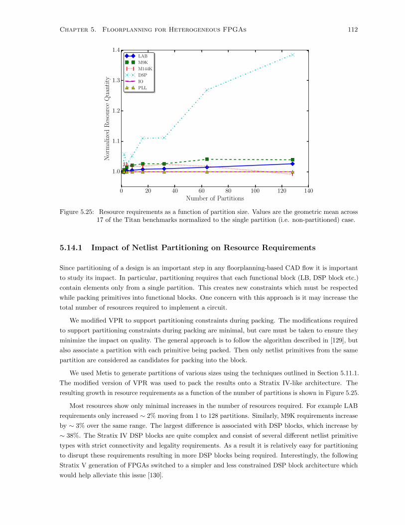
Chapter 5. Floorplanning for Heterogeneous FPGAs 112
0 20 40 60 80 100 120 140
Number of Partitions
1.0
1.1
1.2
1.3
1.4
Nor
mal
ized
Res
ourc
eQ
uan
tity
LAB
M9K
M144K
DSP
IO
PLL
Figure 5.25: Resource requirements as a function of partition size. Values are the geometric mean across17 of the Titan benchmarks normalized to the single partition (i.e. non-partitioned) case.
5.14.1 Impact of Netlist Partitioning on Resource Requirements
Since partitioning of a design is an important step in any floorplanning-based CAD flow it is important
to study its impact. In particular, partitioning requires that each functional block (LB, DSP block etc.)
contain elements only from a single partition. This creates new constraints which must be respected
while packing primitives into functional blocks. One concern with this approach is it may increase the
total number of resources required to implement a circuit.
We modified VPR to support partitioning constraints during packing. The modifications required
to support partitioning constraints during packing are minimal, but care must be taken to ensure they
minimize the impact on quality. The general approach is to follow the algorithm described in [129], but
also associate a partition with each primitive being packed. Then only netlist primitives from the same
partition are considered as candidates for packing into the block.
We used Metis to generate partitions of various sizes using the techniques outlined in Section 5.11.1.
The modified version of VPR was used to pack the results onto a Stratix IV-like architecture. The
resulting growth in resource requirements as a function of the number of partitions is shown in Figure 5.25.
Most resources show only minimal increases in the number of resources required. For example LAB
requirements only increased ∼ 2% moving from 1 to 128 partitions. Similarly, M9K requirements increase
by ∼ 3% over the same range. The largest difference is associated with DSP blocks, which increase by
∼ 38%. The Stratix IV DSP blocks are quite complex and consist of several different netlist primitive
types with strict connectivity and legality requirements. As a result it is relatively easy for partitioning
to disrupt these requirements resulting in more DSP blocks being required. Interestingly, the following
Stratix V generation of FPGAs switched to a simpler and less constrained DSP block architecture which
would help alleviate this issue [130].
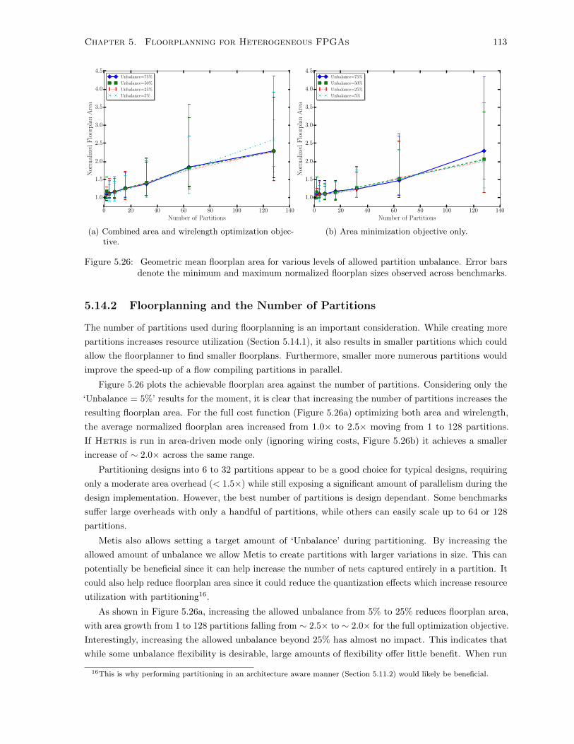
Chapter 5. Floorplanning for Heterogeneous FPGAs 113
0 20 40 60 80 100 120 140
Number of Partitions
1.0
1.5
2.0
2.5
3.0
3.5
4.0
4.5
Nor
mal
ized
Flo
orp
lan
Are
a
Unbalance=75%
Unbalance=50%
Unbalance=25%
Unbalance=5%
(a) Combined area and wirelength optimization objec-tive.
0 20 40 60 80 100 120 140
Number of Partitions
1.0
1.5
2.0
2.5
3.0
3.5
4.0
4.5
Nor
mal
ized
Flo
orp
lan
Are
a
Unbalance=75%
Unbalance=50%
Unbalance=25%
Unbalance=5%
(b) Area minimization objective only.
Figure 5.26: Geometric mean floorplan area for various levels of allowed partition unbalance. Error barsdenote the minimum and maximum normalized floorplan sizes observed across benchmarks.
5.14.2 Floorplanning and the Number of Partitions
The number of partitions used during floorplanning is an important consideration. While creating more
partitions increases resource utilization (Section 5.14.1), it also results in smaller partitions which could
allow the floorplanner to find smaller floorplans. Furthermore, smaller more numerous partitions would
improve the speed-up of a flow compiling partitions in parallel.
Figure 5.26 plots the achievable floorplan area against the number of partitions. Considering only the
‘Unbalance = 5%’ results for the moment, it is clear that increasing the number of partitions increases the
resulting floorplan area. For the full cost function (Figure 5.26a) optimizing both area and wirelength,
the average normalized floorplan area increased from 1.0× to 2.5× moving from 1 to 128 partitions.
If Hetris is run in area-driven mode only (ignoring wiring costs, Figure 5.26b) it achieves a smaller
increase of ∼ 2.0× across the same range.
Partitioning designs into 6 to 32 partitions appear to be a good choice for typical designs, requiring
only a moderate area overhead (< 1.5×) while still exposing a significant amount of parallelism during the
design implementation. However, the best number of partitions is design dependant. Some benchmarks
suffer large overheads with only a handful of partitions, while others can easily scale up to 64 or 128
partitions.
Metis also allows setting a target amount of ‘Unbalance’ during partitioning. By increasing the
allowed amount of unbalance we allow Metis to create partitions with larger variations in size. This can
potentially be beneficial since it can help increase the number of nets captured entirely in a partition. It
could also help reduce floorplan area since it could reduce the quantization effects which increase resource
utilization with partitioning16.
As shown in Figure 5.26a, increasing the allowed unbalance from 5% to 25% reduces floorplan area,
with area growth from 1 to 128 partitions falling from ∼ 2.5× to ∼ 2.0× for the full optimization objective.
Interestingly, increasing the allowed unbalance beyond 25% has almost no impact. This indicates that
while some unbalance flexibility is desirable, large amounts of flexibility offer little benefit. When run
16This is why performing partitioning in an architecture aware manner (Section 5.11.2) would likely be beneficial.

Chapter 5. Floorplanning for Heterogeneous FPGAs 114
0 20 40 60 80 100 120 140
Number of Partitions (N)
0
10
20
30
40
50
60
70
80
90
Nor
mal
ized
Ru
n-t
ime
Run-time
O(N1.56)
Figure 5.27: Hetris geometric mean run-time normalized to a single partition.
with the area optimization objective (Figure 5.26b) large amounts of unbalance (i.e. 75%) result in
larger floorplan area. It is possible that in this scenario the more unbalanced partitions do not match
the underlying architecture as well as the more balanced partitions. For scenarios with fewer than 128
partitions unbalance has little impact.
Varying the number of partitions also allows us to investigate the scalability of Hetris. It is important
to note that increasing the number of partitions not only increases the size of the floorplanning problem
but also increases the number of external nets that must be evaluated by Hetris. For some benchmarks
Hetris required more memory than was available on the machine17. Figure 5.27 shows the measured
run time of Hetris as the number of partitions increases. While the run-time behaviour is super-linear,
it maintains a relatively low average complexity of O(N1.56). Since we perform O(N1.33) moves per
temperature (Section 5.7.3) this illustrates the efficacy of the algorithmic optimizations presented in
Section 5.6 at reducing the average per-move complexity18.
Detailed per-benchmark run-time and QoR results for various numbers of partitions are listed in
Appendix A.
5.14.3 Comparison of Metis and Quartus II Partitions
Since partitioning is an important step in any floorplanning flow, it is useful to compare different methods
for generating partitions. For these experiments we compare the partitions generated by Metis and
Quartus II’s Design Partition Planner. Unlike Metis, Quartus II follows the logical design hierarchy while
17Most of Hetris’s memory is used to memoize IRLs across moves. As noted in Section 5.6.2, the memoization table iscurrently implemented as a cache of unbounded size. Particularly on large benchmarks which explore a large number ofIRLs, this can result in high memory usage. It is expected that appropriately sizing this cache to the problem being solvedwill significantly reduce the memory requirements, with a minimal impact on run-time. However the development of such amethod is left for future work.
18In comparison, Cheng and Wong’s slicing tree evaluation algorithm is reported as being linear in the number of modules,O(N) [56]. This would make the overall complexity of the annealer using their algorithm O(N ·N1.33) = O(N2.33), whichis substantially larger than what we observe here.

Chapter 5. Floorplanning for Heterogeneous FPGAs 115
partitioning. For the comparison, we let Quartus II select the number of partitions to create, and then
configure Metis to generate the same number of partitions under a 25% unbalance constraint.
Benchmark N LABs M9Ks DSPs M144Ks
gsm switch 64 0.97× 0.98× 1.05×SLAM spheric 3 1.00× 1.00× 0.97×segmentation 4 1.00× 1.00× 0.84×
minres 7 0.95× 0.99× 0.70× 0.86×denoise 8 0.99× 1.00× 1.04×mes noc 2 1.00× 1.00×
sparcT1 core 5 0.98× 0.97× 1.00×sparcT2 core 7 1.00× 0.84×
dart 13 0.99× 1.00×openCV 63 0.99× 0.99× 0.90× 1.04×
stereo vision 11 0.98× 0.98× 0.89×GEOMEAN 8.88 0.99× 0.98× 0.90× 0.98×
Table 5.5: Comparision of post-packing resources required by Metis and Quartus II generated partitions.All columns except N (number of partitions) are normalized to the values for Metis’ parititions.
Benchmark NMin.
Partition SizeMax.
Partition SizeAvg.
Partition SizeExternal
Nets
gsm switch 64 1.85× 8.55× 0.68× 0.33×SLAM spheric 3 0.07× 2.12× 0.19× 0.02×segmentation 4 0.52× 2.04× 0.70× 0.03×
minres 7 0.31× 2.67× 0.50× 0.24×denoise 8 1.62× 1.85× 1.02× 0.18×mes noc 2 0.12× 1.74× 0.45× 0.01×
sparcT1 core 5 0.59× 1.10× 0.89× 0.19×sparcT2 core 7 0.28× 1.71× 0.67× 0.13×
dart 13 1.16× 0.96× 0.97× 0.35×openCV 63 2.62× 3.38× 0.96× 0.29×
stereo vision 11 0.92× 3.02× 0.79× 0.45×GEOMEAN 8.88 0.57× 2.20× 0.65× 0.12×
Table 5.6: Comparision of Metis and Quartus II generated partition sizes. All columns except N (numberof partitions) are normalized to the values obtained with Metis’ parititions. The size of apartition is calculated as the sum of the quantity of each block type multiplied by the blocktype’s size (number of grid locations it occupies).
Table 5.5 compares the characteristics of partitions generated by Quartus II and Metis. Looking
first at the number of partitions generated (N) it is clear that Quartus II tends towards generating a
small number of partitions on most designs; however it occasionally chooses a larger number of partitions
for some designs (i.e. gsm switch and openCV). Notably, for some benchmarks (not listed in Table 5.5)
Quartus II elects to leave the entire design in a single partition. Table 5.5 also compares the post-packing
resources required by the Quartus II and Metis partitions. On average Quartus II’s partitions result in
slightly lower resource requirements for LAB, M9K and M144K blocks but reduced the required number of
DSP blocks by a more significant 10%. This is notable since DSP blocks were found to be quite sensitive
to the number of partitions in Section 5.14.2. However it is not clear whether this improvement results
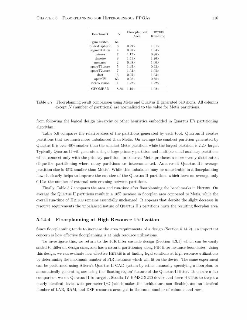
Chapter 5. Floorplanning for Heterogeneous FPGAs 116
Benchmark NFloorplanned
AreaHetris
Run-time
gsm switch 64SLAM spheric 3 0.99× 1.01×segmentation 4 0.88× 1.04×
minres 7 1.17× 0.86×denoise 8 1.51× 1.26×mes noc 2 0.98× 1.00×
sparcT1 core 5 1.45× 0.93×sparcT2 core 7 1.02× 1.05×
dart 13 0.95× 1.03×openCV 63 0.98× 0.88×
stereo vision 11 1.22× 1.22×GEOMEAN 8.88 1.10× 1.02×
Table 5.7: Floorplanning result comparison using Metis and Quartus II generated partitions. All columnsexcept N (number of partitions) are normalized to the value for Metis parititions.
from following the logical design hierarchy or other heuristics embedded in Quartus II’s partitioning
algorithm.
Table 5.6 compares the relative sizes of the partitions generated by each tool. Quartus II creates
partitions that are much more unbalanced than Metis. On average the smallest partition generated by
Quartus II is over 40% smaller than the smallest Metis partition, while the largest partition is 2.2× larger.
Typically Quartus II will generate a single large primary partition and multiple small auxiliary partitions
which connect only with the primary partition. In contrast Metis produces a more evenly distributed,
clique-like partitioning where many partitions are interconnected. As a result Quartus II’s average
partition size is 45% smaller than Metis’. While this unbalance may be undesirable in a floorplanning
flow, it clearly helps to improve the cut size of the Quartus II partitions which have on average only
0.12× the number of external nets crossing between partitions.
Finally, Table 5.7 compares the area and run-time after floorplanning the benchmarks in Hetris. On
average the Quartus II partitions result in a 10% increase in floorplan area compared to Metis, while the
overall run-time of Hetris remains essentially unchanged. It appears that despite the slight decrease in
resource requirements the unbalanced nature of Quartus II’s partitions hurts the resulting floorplan area.
5.14.4 Floorplanning at High Resource Utilization
Since floorplanning tends to increase the area requirements of a design (Section 5.14.2), an important
concern is how effective floorplanning is at high resource utilizations.
To investigate this, we return to the FIR filter cascade design (Section 4.3.1) which can be easily
scaled to different design sizes, and has a natural partitioning along FIR filter instance boundaries. Using
this design, we can evaluate how effective Hetris is at finding legal solutions at high resource utilizations
by determining the maximum number of FIR instances which will fit on the device. The same experiment
can be performed using Altera’s Quartus II CAD system by either manually specifying a floorplan, or
automatically generating one using the ‘floating region’ feature of the Quartus II fitter. To ensure a fair
comparison we set Quartus II to target a Stratix IV EP4SGX230 device and force Hetris to target a
nearly identical device with perimeter I/O (which makes the architecture non-tileable), and an identical
number of LAB, RAM, and DSP resources arranged in the same number of columns and rows.

Chapter 5. Floorplanning for Heterogeneous FPGAs 117
PartitioningMethodology
Required DSP Blocksper Partition
Effective DSPBlocks per FIR
Number of Partitionson EP4SGX230
Maximum FIR Instanceson EP4SGX230
Flat — 3.25 1 491-FIR per Partition 4 4.00 40 402-FIR per Partition 7 3.50 23 463-FIR per Partition 10 3.33 16 484-FIR per Partition 13 3.25 12 48
Table 5.8: Impact of partitioning on FIR Cascade DSP Requirements targeting EP4SGX230 (161 DSPblocks). Each FIR instance requires 26 multipliers, constituting 3.25 DSP blocks.
The FIR cascade design is limited by the available number of DSP blocks on the device. Table 5.8
shows the resource requirements for the different partitioning configurations as well as the maximum
number of instances that could (theoretically) fit on the device. The round-off caused by partitioning
(since blocks can not be assigned to multiple partitions) can have a significant impact on the maximum
number of FIR instances that will fit on the device.
Flow Max FIR Inst. Time (s) Note
QII Flat 49 —QII Partitioned + Manual FP 40 2,700.0 Required ‘L’ shaped region
QII Partitioned + Floating Region 37 — Floorplanning time not reported by QIIHetris Default 38 53.9 inner num = 2
Hetris High Effort 38 117.5 inner num = 5Hetris High Effort + Ignore IntWL 39 135.3 inner num = 5 and Cfac = 0 in Equation (5.4)
Table 5.9: Maximum number of FIRs for which legal floorplans were found in Quartus II and Hetris.Both the QII partitioned and Hetris results used 1-FIR per Partition.
The results of floorplanning with a single FIR per partition are shown in Table 5.9. Flat compilation
packs the most instances onto the device, primarily because it doesn’t suffer from partitioning round-off
effects. Considering the approaches using partitioning, only manual floorplanning is able to fit the
theoretical maximum number of instances. To do so required a non-rectangular ’L’ shaped region,
highlighted in Figure 5.28. Manual floorplanning required approximately 45 minutes to identify a good
floorplan and enter it into the tool. Of the automated methods, Quartus II’s floating regions perform the
worst, packing only 37 FIR instances onto the device. Hetris performs better, finding solutions for 38
instances by default and for 39 at a higher effort level and relaxed the Internal Wirelength (WL) (i.e.
module aspect ratio) requirements. The floorplan for 39 FIR instances generated by Hetris is shown in
Figure 5.29. As expected, using automated approaches requires much less time (∼ 20×) than manual
floorplanning19.
Table 5.10 shows some of the impact of the different partitioning techniques from Table 5.8. Hetris
is able to pack more FIR instances than Quartus II for both the 1-FIR and 2-FIR configurations20.
19The FIR design is relatively straightforward to manually floorplan, even at high resource utilization. It has identicalresource requirements for each partition and very regular connectivity between modules. For a more heterogeneous set ofpartitions with competing connectivity requirements the process would be significantly more difficult to perform manually.
20For the 3-FIR and 4-FIR cases Hetris is at a disadvantage since VPR’s packing requires more DSP blocks than QuartusII’s. As a result Quartus II was able to fit either 3 or 4 more FIR instances in these cases. These difference reflects VPR’spacking quality and not Hetris’s ability to find legal floorplans. Interestingly, in the 3-FIR case Hetris is able to fit thetheoretical maximum number of instances on the device given VPR’s packing. In contrast Quartus II was never able to fitthe theoretical maximum number of instances for any of the evaluated floorplanning configurations.

Chapter 5. Floorplanning for Heterogeneous FPGAs 118
L-shaped
Region
Figure 5.28: Manual floorplan in Quartus II of 40 partitioned FIR instances targeting an EP4SGX230device. To fit the final instance (Region 39) an ‘L’ shaped region is required.
Figure 5.29: Floorplan generated by Hetris for 39 partitioned FIR instances targeting an EP4SGX230device.
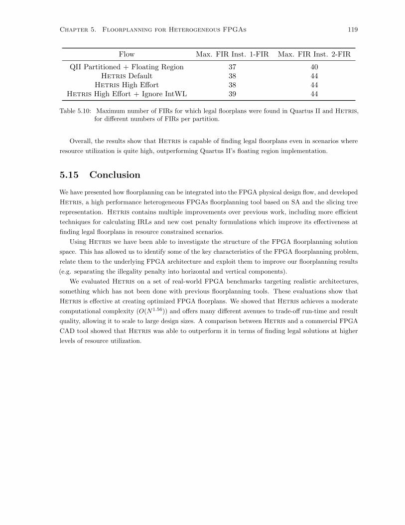
Chapter 5. Floorplanning for Heterogeneous FPGAs 119
Flow Max. FIR Inst. 1-FIR Max. FIR Inst. 2-FIR
QII Partitioned + Floating Region 37 40Hetris Default 38 44
Hetris High Effort 38 44Hetris High Effort + Ignore IntWL 39 44
Table 5.10: Maximum number of FIRs for which legal floorplans were found in Quartus II and Hetris,for different numbers of FIRs per partition.
Overall, the results show that Hetris is capable of finding legal floorplans even in scenarios where
resource utilization is quite high, outperforming Quartus II’s floating region implementation.
5.15 Conclusion
We have presented how floorplanning can be integrated into the FPGA physical design flow, and developed
Hetris, a high performance heterogeneous FPGAs floorplanning tool based on SA and the slicing tree
representation. Hetris contains multiple improvements over previous work, including more efficient
techniques for calculating IRLs and new cost penalty formulations which improve its effectiveness at
finding legal floorplans in resource constrained scenarios.
Using Hetris we have been able to investigate the structure of the FPGA floorplanning solution
space. This has allowed us to identify some of the key characteristics of the FPGA floorplanning problem,
relate them to the underlying FPGA architecture and exploit them to improve our floorplanning results
(e.g. separating the illegality penalty into horizontal and vertical components).
We evaluated Hetris on a set of real-world FPGA benchmarks targeting realistic architectures,
something which has not been done with previous floorplanning tools. These evaluations show that
Hetris is effective at creating optimized FPGA floorplans. We showed that Hetris achieves a moderate
computational complexity (O(N1.56)) and offers many different avenues to trade-off run-time and result
quality, allowing it to scale to large design sizes. A comparison between Hetris and a commercial FPGA
CAD tool showed that Hetris was able to outperform it in terms of finding legal solutions at higher
levels of resource utilization.
Chapter 6
Conclusion and Future Work
In this thesis, we have presented three major components:
1. The Titan design flow and Titan23 benchmark suite (Chapter 3),
2. An evaluation of LI design methodologies targeting FPGAs (Chapter 4), and finally
3. Hetris, an automated floorplanning tool for heterogeneous FPGAs (Chapter 5)
In this concluding chapter we discuss the key conclusions from each of these components, and future
research directions.
6.1 Titan Flow and Benchmarks
The Titan flow and benchmarks address significant needs in FPGAs research: the need for large-scale
modern benchmarks, and the need for a realistic comparison between academic and state-of-the-art
industrial CAD tools.
The Titan flow enables broad HDL coverage, significantly easing the process of bringing real-world
benchmarks into an academic CAD environment. The Titan23 benchmark suite is a collection of
benchmarks which are both much larger (215× larger compared to the MCNC20) and more realistic
(exploiting the heterogeneous resources of modern FPGAs) than those previously used. Using large scale
heterogeneous benchmarks is important, since it ensures that empirical research conclusions made during
FPGA CAD and architecture research are robust and relevant to real-world practice.
By creating an accurate architecture capture of the commercial Stratix IV FPGA architecture, it was
also possible to compare a popular academic CAD tool (VPR), with a state-of-the-art commercial tools
(Altera’s Quartus II) using the Titan23 benchmark suite. This comparison showed that commercial tools
can significantly outperform academic tools. From a computational resources perspective, compared to
Quartus II, VPR required 2.8× more run-time, and 6.2× more memory. From a quality perspective,
VPR required 2.2× more wire, and the resulting circuits ran 1.5× slower. VPR’s focus on packing density
was identified as the key component responsible for the quality difference, while slow routing convergence
times were responsible for a large part of the run-time difference. The comparison also showed that both
commercial and academic tools struggle with long run-times on the largest benchmarks.
120
Chapter 6. Conclusion and Future Work 121
6.1.1 Titan Future Work
Given the substantial gap between VPR and commercial FPGA CAD tools, it is clear that there remains
significant room for improvement in the run time, memory usage, and result quality of VPR. Specific
areas to focus on in VPR include packing for wireability instead of density, and faster routing convergence
with timing optimizations. Closing this gap in both VPR and other academic tools is important if
academic research is to remain relevant to real-world systems. That commercial tools also struggle on
large designs continues to motivate further research into improved algorithms and design flows.
While the Titan23 benchmark suite represents a first step forward, it is important that it be kept up
to date. Any benchmark suite will need to be continually updated to keep pace with increasing FPGA
design size and complexity, and to ensure benchmarks exploit new architectural features. It would also
be beneficial to increase the breadth of applications included in the benchmark suite, in particular with
industrial benchmarks.
While the Titan flow enables designs to be extracted from a commercial tool and used in an academic
environment, it would be very useful to perform the reverse procedure. For instance, being able to
perform part of the physical design implementation (e.g. placement) in an academic tool, and then export
the results to a commercial tool would bring multiple benefits. It would allow academic researchers
to confirm the accuracy of their models against industrial-strength tools for operations such as timing
analysis and power estimation. Furthermore, it would allow academic tools to extend and augment the
functionality of commercial flows and target real devices.
6.2 Latency Insensitive Design
The growing gap between local and system-level interconnect speeds is making alternative design
methodologies such as LI design, which promise to simplify timing closure, increasingly important.
However a key consideration when adopting such a methodology is the overheads associated with it. We
investigated dynamically scheduled LI design targeting FPGAs, and quantified its area and frequency
overheads.
To reduce the frequency overhead, we developed a new pipelined LI shell, which is able to handle
FPGA specific considerations (such as high-fanout clock enables) with minimal frequency overhead. We
also identified that area overhead is generally dominated by the FIFO queues required at shell inputs.
This makes increasing the number of input ports, or input port width, expensive. In contrast, increasing
the depth of the FIFO queues was low cost due to the large size of the on-chip RAM blocks.
Finally, to investigate the system-level impact of applying LI design techniques we extrapolated our
results using Rent’s rule to estimate the area overhead for varying levels of communication locality and
granularity. The results show that the area overheads of LI design methods can be reasonable for systems
that exhibit well localized communication, but grow as communication locality decreases. As a result,
for systems with poorly localized communication the LI communication granularity would need to be
increased to keep overheads reasonable.
LID will always have a cost in area and frequency compared to a perfectly hand pipelined non-LI
system. As design sizes continue to grow, the increasing design costs of such ‘perfect’ systems will make
LID approaches increasingly attractive. However, to fully exploit the promise and benefits of LID it must
be integrated into CAD flows and automatically exploited by CAD tools to improve designer productivity
and design quality.
Chapter 6. Conclusion and Future Work 122
6.2.1 Latency Insensitive Design Future Work
While our results show that LI design is practical using current hardware and techniques, further work to
develop higher performing and lower area overhead LI systems would be beneficial. One potential method
would be to improve support for low-cost FIFOs in future FPGA architectures. Another interesting
approach would be to investigate less flexible LI implementations. While fully statically scheduled LI
systems are likely too restrictive, a middle ground approach could yield better trade-offs between design
flexibility and overhead. In particular, systems which restrict a link’s communication latency to fall
within a finite range appear promising. Since support for unbounded latency would not be required,
some of the overheads of fully dynamic LID could be reduced, while still offering more flexibility than
static scheduling.
It would also be useful to extend the overhead quantification to include a power analysis of LID,
particularly since unlike ASICs, stalled modules on FPGAs do not have their clocks gated. Similarly
further work on evaluating the holistic costs and benefits of LID on real world systems, with larger and
more complex benchmarks, would be of value.
6.3 Floorplanning
Floorplanning offers multiple potential benefits to the FPGA design process including: improving
the scalability of existing CAD algorithms, providing early feedback to designers about the physical
characteristics of their systems and improved decoupling between parts of complex systems. To this
end we have developed Hetris, an automated FPGA floorplanning tool based on SA and the slicing
tree representation. Hetris contains several algorithmic improvements which improve its scalability
compared to previous work including: incremental IRL calculation, memoization of IRL across moves
and new cost functions to handle legality constraints.
Using Hetris we investigated the impact of floorplanning on the FPGA design flow, and identified
some of the key characteristics of the FPGA floorplanning problem and how they relate to the underlying
FPGA architecture. We evaluated Hetris on the Titan benchmarks and investigated the impact of
different automated partitioning techniques. When compared in high resource utilization scenarios,
Hetris was able to outperform a commercial tool, packing more resources onto a nearly full device. This
is also the first evaluation of a heterogeneous FPGA floorplanner using realistic FPGA benchmarks.
6.3.1 Floorplanning Future Work
There are a number of open questions regarding floorplanning for FPGAs with many different avenues
for future work to explore.
IRL Memoization
As noted in Section 5.6.2 Hetris memoizes all intermediately calculated IRLs. One limitation of this
approach is that it can result in large memory consumption if many IRLs are explored during the anneal.
Using a finite sized cache would help limit memory consumption at the cost of re-calculating rarely used
IRLs. How to size such a cache to a given floorplanning problem, and what eviction policy to use remain
open questions.

Chapter 6. Conclusion and Future Work 123
Alternate Slicing Tree Evaluation Algorithms
While Hetris currently uses efficient algorithms to calculate IRLs, there are numerous alternative
approaches and optimizations which have not been explored.
The core slicing tree evaluation algorithm calculates a list of potential floorplans at the root node of
the slicing tree. Of these calculated floorplans, currently only the smallest is returned to the annealer for
actual evaluation of wirelength metrics. Using a more intelligent approach to select the ‘best’ floorplan
from an IRL would likely improve the results. Fully evaluating each potential floorplan would likely
produce the best result but would be computationally expensive, reducing the number of slicing trees
explored in an equivalent amount of run-time. It would be interesting to investigate whether this approach,
which more thoroughly optimizes a few parts of the solution space, would be more effective than the
approach currently used in Hetris. An alternative approach would be to return legal floorplans first
(rather than the smallest) if they exist. This would assist the floorplanner in finding legal solutions more
quickly, limiting the amount of time the annealer spends ‘stalled’ – improving run-time.
As noted above, in the current algorithm multiple floorplans are found for each slicing tree - but
only one is returned to the annealer for evaluation. This follows from the formulation of the slicing
tree evaluation as a dynamic programming problem. In order to find the smallest area floorplan for
a particular slicing tree, we must consider multiple shapes for every partition and super-partition in
the design. While this ensures area-minimal solutions are found if they exist, many of the resulting
computations are unused, wasting computational effort. If we are willing to give-up on the ‘optimal’
nature of our slicing tree evaluation algorithm we could abandon the dynamic programming approach in
favour of a (likely much faster) greedy heuristic approach.
One limitation of such a heuristic approach is that it may not explore a sufficient amount of the
solution space, leading to poor result quality. However, this could be addressed by modifying the annealer.
For instance, the slicing tree representation could be extended so that each leaf node also has a ‘target
aspect ratio’ which is adjusted by the annealer using new types of moves. This hoists the responsibility
for considering different region shapes out of the slicing tree evaluation algorithm and into the annealer.
While it would likely require more moves to converge to a solution, each move would be faster, and
the annealer, which has a more informed global view of the problem than the slicing tree evaluation
algorithm, may be able to find better solutions.
Whether these alternative approaches, or others, provide better run-time/quality trade-offs is an
important avenue for future investigation.
Several of the tuning parameters which control the run-time/quality trade offs in Hetris, such
as aspect ratio limits and the IRL dimension limit are currently set manually. Investigating ways of
automatically adjusting these could improve the robustness of Hetris, while investigating new techniques
to dynamically adjust them during the anneal (e.g. limiting the IRL dimension limit once legality is
achieved) could further improve tool run-time and result quality.
Different Floorplan Representations
Hetris uses the slicing tree representation to encode the solution space. Since slicing floorplans are one
of the most restricted sets of representations, it would be interesting to investigate the impact of other,
more general representations and the trade-offs they offer in terms of quality and run-time.
As noted in Section 5.14.4, it is sometimes only possible find a legal floorplan by using non-rectangular

Chapter 6. Conclusion and Future Work 124
shapes (e.g. ‘L’ or ‘T’), which are not supported natively by most floorplanning representations. These
shapes may be particularly important for FPGAs, since they can be required in order to find a legal
solution due to the fixed heterogeneous resources of an FPGA1. One approach would be to identify
partitions which struggle to find good positions with conventional rectangular shapes, and fracture them
into two or more rectangular regions which are constrained to remain adjacent. This dynamic ‘union
of rectangles’ approach allows conventional rectangular floorplanning representations to mimic more
complex shapes. While techniques to handle these types of constraints have been studied in ASICs [131],
it is not clear if the same techniques can be used on FPGAs due to their heterogeneous nature.
Additional Optimization Objectives
Currently Hetris only attempts to optimizes for area and wirelength, neglecting important optimization
objectives such as timing. It is therefore important that future work extend Hetris to support timing-
driven floorplanning, to optimize the performance of the generated floorplan. Similarly, other potential
extensions include optimizing for power and routability. Additionally some of the cost metrics (in
particular the internal wirelength metric) have not been extensively investigated, so research into modified
or alternative metrics would also be beneficial.
Bus Planning
A common technique used in ASIC floorplanning is to pre-plan the routing of large data buses during
floorplanning. This has the advantage of generating more predictable results, since these important
structures are fixed early in the design process. This can help designers achieve better performance in
fewer design iterations. Integrating bus planning into an FPGA based floorplanning flow could potentially
yield similar benefits.
Design Partitioning Techniques
Design partitioning is an important part of the floorplanning process that has seen little study. While
we reported the impact of automated partitioning using Metis, we also identified the architecture-aware
partitioning problem which is not addressed by current partitioning tools.
Additionally, floorplanning using manually partitioned designs which follow the design hierarchy
should also be studied. This style of partitioning is important for designers using floorplanning to enable
multiple teams to work in parallel.
Full Flow Evaluation
The results presented for Hetris have focused only on quality metrics that can be evaluated directly
after floorplanning such as floorplan area. Since most of the physical implementation (e.g. placement
and routing) has not been performed we can draw only limited conclusions about the overall quality of a
specific floorplan.
It is therefore important that future work evaluates floorplanning in the context of the full design flow.
This will allow the impact of floorplanning on important metrics such as routed wirelength, timing and
power consumption to be quantified. Performing these evaluations is likely to be key in determining what
characterizes a high quality floorplan and enabling further improvements. Similarly, since enabling parallel
1This is unlike ASICs, where such shapes are only helpful for area minimization.

Chapter 6. Conclusion and Future Work 125
implementation of the floorplanned components is one of the key objectives of a floorplanning-based design
flow, it will be important to measure and quantify the impact of parallel compilation with floorplans on
the total run-time and memory requirements of the design flow.
Additionally, so far Hetris has only been evaluated on Stratix IV like architectures; further evaluation
targeting different architectures would be illuminating.
6.4 Looking Forward
Finally, looking forward we believe that floorplanning and LI design are complementary techniques
that facilitate a divide-and-conquer approach to design. Floorplanning allows us to decompose a design
into spatially independent parts, while LI design decouples those components from each other’s timing
requirements. It would therefore be interesting to study how these techniques can be used together. One
approach would be to make floorplanning aware of LI which, combined with timing-driven floorplanning,
will enable new optimizations to be performed during floorplanning, such as pipelining long timing-
critical connections. This combined approach would enable new design flexibility and improve designer
productivity by helping to automate timing closure.

Appendix A
Detailed Floorplanning Results
This appendix provides detailed QoR and run-time data for Hetris while varying the number of partitions
to be floorplanned with a target unbalance between partitions of 5%.
Table A.1 details the run-time of Hetris for various problem sizes. Note that increasing the number
of partitions results in each benchmark being divided into smaller partitions. As a result more nets cross
between partitions increasing the HPWL calculation time.
Benchmark N = 1 N = 2 N = 4 N = 8 N = 16 N = 32 N = 64 N = 128
mes noc 3.66 (1.00×) 4.19 (1.15×) 4.42 (1.21×) 7.59 (2.08×) 22.29 (6.10×) 66.30 (18.14×)gsm switch 1.76 (1.00×) 1.89 (1.07×) 2.45 (1.39×) 3.39 (1.93×) 7.73 (4.39×) 20.97 (11.92×) 85.45 (48.59×)
cholesky bdti 1.75 (1.00×) 1.77 (1.01×) 2.00 (1.14×) 2.39 (1.36×) 4.16 (2.38×) 9.38 (5.36×) 21.13 (12.06×) 42.99 (24.54×)denoise 1.58 (1.00×) 1.78 (1.13×) 2.00 (1.27×) 3.07 (1.95×) 7.60 (4.82×) 16.52 (10.49×) 41.31 (26.22×) 107.97 (68.52×)stap qrd 1.34 (1.00×) 1.43 (1.07×) 1.72 (1.29×) 2.74 (2.05×) 7.16 (5.35×) 16.91 (12.65×) 57.20 (42.76×)
sparcT2 core 1.19 (1.00×) 1.23 (1.03×) 1.57 (1.31×) 2.62 (2.20×) 7.62 (6.39×) 22.19 (18.61×) 62.40 (52.33×)minres 0.93 (1.00×) 1.11 (1.19×) 1.50 (1.62×) 2.22 (2.40×) 4.97 (5.36×) 10.91 (11.77×) 26.40 (28.48×) 78.01 (84.15×)
openCV 0.88 (1.00×) 0.89 (1.01×) 0.96 (1.09×) 1.21 (1.37×) 2.26 (2.58×) 5.36 (6.11×) 17.43 (19.85×) 62.78 (71.46×)bitonic mesh 0.80 (1.00×) 0.93 (1.16×) 1.02 (1.27×) 1.53 (1.90×) 1.90 (2.36×) 3.59 (4.46×) 19.70 (24.49×) 76.87 (95.58×)
dart 0.78 (1.00×) 0.74 (0.95×) 0.90 (1.15×) 1.26 (1.62×) 2.63 (3.38×) 13.05 (16.78×) 58.96 (75.80×)segmentation 0.70 (1.00×) 0.82 (1.18×) 1.04 (1.48×) 1.63 (2.33×) 3.34 (4.77×) 13.78 (19.69×) 19.66 (28.08×)SLAM spheric 0.61 (1.00×) 0.62 (1.02×) 0.88 (1.44×) 1.71 (2.82×) 2.73 (4.48×) 9.11 (14.97×) 23.04 (37.88×)cholesky mc 0.50 (1.00×) 0.58 (1.17×) 0.72 (1.44×) 0.95 (1.90×) 2.13 (4.25×) 3.68 (7.36×) 11.89 (23.79×) 45.11 (90.28×)
des90 0.49 (1.00×) 0.51 (1.03×) 0.55 (1.11×) 0.73 (1.47×) 1.33 (2.70×) 2.89 (5.85×) 11.66 (23.62×) 51.00 (103.35×)sparcT1 core 0.34 (1.00×) 0.37 (1.09×) 0.48 (1.40×) 0.78 (2.27×) 2.27 (6.61×) 7.14 (20.78×) 20.64 (60.07×) 87.75 (255.34×)
neuron 0.32 (1.00×) 0.34 (1.07×) 0.42 (1.31×) 0.70 (2.18×) 1.28 (4.00×) 2.64 (8.21×) 7.05 (21.95×) 32.75 (101.92×)stereo vision 0.32 (1.00×) 0.34 (1.07×) 0.41 (1.30×) 0.67 (2.10×) 1.17 (3.68×) 2.79 (8.77×) 8.41 (26.47×) 42.81 (134.76×)
GEOMEAN 0.84 (1.00×) 0.91 (1.08×) 1.09 (1.30×) 1.65 (1.96×) 3.46 (4.11×) 8.96 (10.65×) 23.85 (31.07×) 58.81 (89.13×)
Table A.1: Hetris run-time in minutes, for various numbers of partitions (N). Bracketed values arenormalized to the single partition case. Benchmarks with no results exceeded the memoryavailable on a 64GB machine.
Tables A.2 to A.4 list the per-benchmark area, half-perimeter external wirelength and internal
wirelength respectively. It is important to note that the external wirelength values are not directly
comparable across different numbers of partitions, since the nets involved change with the number of
partitions. Similarly the internal wirelength metric also varies with the number of partitions.
126
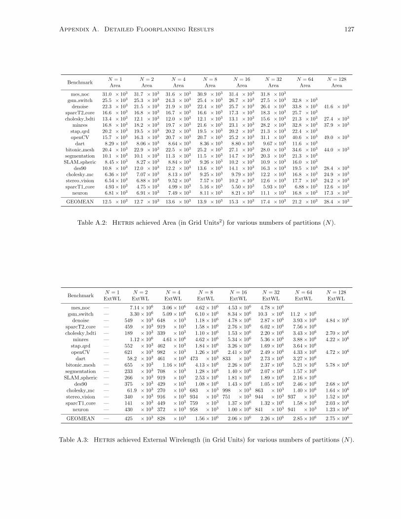
Appendix A. Detailed Floorplanning Results 127
BenchmarkN = 1Area
N = 2Area
N = 4Area
N = 8Area
N = 16Area
N = 32Area
N = 64Area
N = 128Area
mes noc 31.0 × 10³ 31.7 × 10³ 31.6 × 10³ 30.9 × 10³ 31.4 × 10³ 31.8 × 10³
gsm switch 25.5 × 10³ 25.3 × 10³ 24.3 × 10³ 25.4 × 10³ 26.7 × 10³ 27.5 × 10³ 32.8 × 10³
denoise 22.3 × 10³ 21.5 × 10³ 21.9 × 10³ 22.4 × 10³ 25.7 × 10³ 26.4 × 10³ 33.8 × 10³ 41.6 × 10³
sparcT2 core 16.6 × 10³ 16.8 × 10³ 16.7 × 10³ 16.6 × 10³ 17.3 × 10³ 18.3 × 10³ 25.7 × 10³
cholesky bdti 13.4 × 10³ 12.1 × 10³ 12.0 × 10³ 12.1 × 10³ 13.1 × 10³ 15.6 × 10³ 21.3 × 10³ 27.4 × 10³
minres 16.8 × 10³ 18.2 × 10³ 19.7 × 10³ 21.6 × 10³ 23.1 × 10³ 28.2 × 10³ 32.8 × 10³ 37.9 × 10³
stap qrd 20.2 × 10³ 19.5 × 10³ 20.2 × 10³ 19.5 × 10³ 20.2 × 10³ 21.3 × 10³ 22.4 × 10³
openCV 15.7 × 10³ 16.3 × 10³ 20.7 × 10³ 20.7 × 10³ 25.2 × 10³ 31.1 × 10³ 40.6 × 10³ 49.0 × 10³
dart 8.29× 10³ 8.06× 10³ 8.64× 10³ 8.36× 10³ 8.80× 10³ 9.67× 10³ 11.6 × 10³
bitonic mesh 20.4 × 10³ 22.9 × 10³ 22.5 × 10³ 25.2 × 10³ 27.1 × 10³ 28.0 × 10³ 34.6 × 10³ 44.0 × 10³
segmentation 10.1 × 10³ 10.1 × 10³ 11.3 × 10³ 11.5 × 10³ 14.7 × 10³ 20.3 × 10³ 21.3 × 10³
SLAM spheric 8.45× 10³ 8.27× 10³ 8.84× 10³ 9.26× 10³ 10.2 × 10³ 10.9 × 10³ 16.0 × 10³
des90 10.8 × 10³ 12.0 × 10³ 12.2 × 10³ 13.6 × 10³ 14.1 × 10³ 16.3 × 10³ 19.5 × 10³ 28.4 × 10³
cholesky mc 6.36× 10³ 7.07× 10³ 8.13× 10³ 9.25× 10³ 9.79× 10³ 12.2 × 10³ 16.8 × 10³ 24.9 × 10³
stereo vision 6.54× 10³ 6.88× 10³ 9.52× 10³ 7.57× 10³ 10.2 × 10³ 12.6 × 10³ 17.7 × 10³ 24.2 × 10³
sparcT1 core 4.93× 10³ 4.75× 10³ 4.99× 10³ 5.16× 10³ 5.50× 10³ 5.93× 10³ 6.88× 10³ 12.6 × 10³
neuron 6.81× 10³ 6.91× 10³ 7.49× 10³ 8.11× 10³ 8.21× 10³ 11.1 × 10³ 16.8 × 10³ 17.3 × 10³
GEOMEAN 12.5 × 10³ 12.7 × 10³ 13.6 × 10³ 13.9 × 10³ 15.3 × 10³ 17.4 × 10³ 21.2 × 10³ 28.4 × 10³
Table A.2: Hetris achieved Area (in Grid Units2) for various numbers of partitions (N).
BenchmarkN = 1ExtWL
N = 2ExtWL
N = 4ExtWL
N = 8ExtWL
N = 16ExtWL
N = 32ExtWL
N = 64ExtWL
N = 128ExtWL
mes noc — 7.14× 10⁶ 3.06× 10⁶ 4.62× 10⁶ 4.53× 10⁶ 4.78× 10⁶
gsm switch — 3.30× 10⁶ 5.09× 10⁶ 6.10× 10⁶ 8.34× 10⁶ 10.3 × 10⁶ 11.2 × 10⁶
denoise — 549 × 103 648 × 103 1.18× 10⁶ 4.78× 10⁶ 2.87× 10⁶ 3.93× 10⁶ 4.84× 10⁶
sparcT2 core — 459 × 103 919 × 103 1.58× 10⁶ 2.76× 10⁶ 6.02× 10⁶ 7.56× 10⁶
cholesky bdti — 189 × 103 339 × 103 1.10× 10⁶ 1.53× 10⁶ 2.20× 10⁶ 3.43× 10⁶ 2.70× 10⁶
minres — 1.12× 10⁶ 4.61× 10⁶ 4.62× 10⁶ 5.34× 10⁶ 5.36× 10⁶ 3.88× 10⁶ 4.22× 10⁶
stap qrd — 552 × 103 462 × 103 1.84× 10⁶ 3.26× 10⁶ 1.69× 10⁶ 3.64× 10⁶
openCV — 621 × 103 982 × 103 1.26× 10⁶ 2.41× 10⁶ 2.49× 10⁶ 4.33× 10⁶ 4.72× 10⁶
dart — 58.2 × 10³ 461 × 103 473 × 103 833 × 103 2.73× 10⁶ 3.27× 10⁶
bitonic mesh — 655 × 103 1.16× 10⁶ 4.13× 10⁶ 2.26× 10⁶ 2.37× 10⁶ 5.21× 10⁶ 5.78× 10⁶
segmentation — 233 × 103 708 × 103 1.28× 10⁶ 1.40× 10⁶ 2.07× 10⁶ 1.57× 10⁶
SLAM spheric — 266 × 103 919 × 103 2.53× 10⁶ 1.81× 10⁶ 1.89× 10⁶ 2.16× 10⁶
des90 — 375 × 103 429 × 103 1.08× 10⁶ 1.43× 10⁶ 1.05× 10⁶ 2.46× 10⁶ 2.68× 10⁶
cholesky mc — 61.9 × 10³ 270 × 103 683 × 103 998 × 103 863 × 103 1.40× 10⁶ 1.64× 10⁶
stereo vision — 340 × 103 916 × 103 934 × 103 751 × 103 944 × 103 937 × 103 1.52× 10⁶
sparcT1 core — 141 × 103 449 × 103 759 × 103 1.37× 10⁶ 1.32× 10⁶ 1.58× 10⁶ 2.03× 10⁶
neuron — 430 × 103 372 × 103 958 × 103 1.00× 10⁶ 841 × 103 941 × 103 1.23× 10⁶
GEOMEAN — 425 × 103 828 × 103 1.56× 10⁶ 2.06× 10⁶ 2.26× 10⁶ 2.85× 10⁶ 2.75× 10⁶
Table A.3: Hetris achieved External Wirelength (in Grid Units) for various numbers of partitions (N).

Appendix A. Detailed Floorplanning Results 128
BenchmarkN = 1IntWL
N = 2IntWL
N = 4IntWL
N = 8IntWL
N = 16IntWL
N = 32IntWL
N = 64IntWL
N = 128IntWL
mes noc 74.7 × 10³ 63.9 × 10³ 62.9 × 10³ 65.8 × 10³ 64.9 × 10³ 62.9 × 10³
gsm switch 107 × 103 48.4 × 10³ 47.8 × 10³ 51.8 × 10³ 53.5 × 10³ 61.0 × 10³ 67.0 × 10³
denoise 47.7 × 10³ 49.5 × 10³ 43.1 × 10³ 45.7 × 10³ 49.4 × 10³ 52.9 × 10³ 67.3 × 10³ 76.7 × 10³
sparcT2 core 52.6 × 10³ 33.6 × 10³ 33.1 × 10³ 35.3 × 10³ 36.9 × 10³ 39.3 × 10³ 48.6 × 10³
cholesky bdti 46.9 × 10³ 24.2 × 10³ 24.9 × 10³ 24.5 × 10³ 30.4 × 10³ 30.0 × 10³ 38.3 × 10³ 52.1 × 10³
minres 52.7 × 10³ 40.6 × 10³ 41.0 × 10³ 45.8 × 10³ 49.1 × 10³ 54.8 × 10³ 61.9 × 10³ 64.4 × 10³
stap qrd 40.1 × 10³ 45.8 × 10³ 41.7 × 10³ 46.6 × 10³ 41.6 × 10³ 48.6 × 10³ 44.6 × 10³
openCV 63.8 × 10³ 31.6 × 10³ 40.9 × 10³ 41.1 × 10³ 46.4 × 10³ 58.0 × 10³ 59.7 × 10³ 63.9 × 10³
dart 17.1 × 10³ 18.7 × 10³ 17.3 × 10³ 19.6 × 10³ 19.0 × 10³ 22.0 × 10³ 20.6 × 10³
bitonic mesh 76.9 × 10³ 48.6 × 10³ 53.1 × 10³ 49.2 × 10³ 56.3 × 10³ 59.5 × 10³ 53.0 × 10³ 68.8 × 10³
segmentation 29.1 × 10³ 20.7 × 10³ 23.0 × 10³ 25.0 × 10³ 28.6 × 10³ 33.8 × 10³ 47.6 × 10³
SLAM spheric 19.0 × 10³ 19.2 × 10³ 16.4 × 10³ 20.8 × 10³ 18.8 × 10³ 26.3 × 10³ 30.5 × 10³
des90 24.7 × 10³ 28.5 × 10³ 22.5 × 10³ 31.7 × 10³ 27.8 × 10³ 34.7 × 10³ 35.8 × 10³ 33.9 × 10³
cholesky mc 26.7 × 10³ 32.9 × 10³ 16.2 × 10³ 17.5 × 10³ 21.5 × 10³ 28.6 × 10³ 31.5 × 10³ 33.3 × 10³
stereo vision 24.1 × 10³ 15.6 × 10³ 18.9 × 10³ 17.3 × 10³ 19.6 × 10³ 21.0 × 10³ 29.1 × 10³ 24.1 × 10³
sparcT1 core 10.2 × 10³ 17.0 × 10³ 11.5 × 10³ 10.1 × 10³ 10.4 × 10³ 14.1 × 10³ 16.8 × 10³ 17.7 × 10³
neuron 34.1 × 10³ 19.8 × 10³ 14.8 × 10³ 17.2 × 10³ 14.3 × 10³ 21.1 × 10³ 25.1 × 10³ 18.9 × 10³
GEOMEAN 37.2 × 10³ 30.0 × 10³ 27.5 × 10³ 29.5 × 10³ 30.6 × 10³ 35.9 × 10³ 39.2 × 10³ 39.9 × 10³
Table A.4: Hetris achieved Internal Wirelength (in Grid Units2) for various numbers of partitions (N).
Bibliography
[1] G. Moore. “Cramming More Components Onto Integrated Circuits.” Proceedings of the IEEE,
86 (1), pp. 82–85, 1998. doi:10.1109/JPROC.1998.658762.
[2] G. Moore. “Progress in Digital Integrated Electronics.” In International Electron Devices Meeting,
volume 21, pp. 11–13. 1975.
[3] “System Drivers.” Technical report, International Technology Roadmap for Semiconductors (ITRS),
2011.
[4] “Design.” Technical report, International Technology Roadmap for Semiconductors (ITRS), 2011.
[5] J. Richardson, et al. “Comparative analysis of HPC and accelerator devices: Computation, memory,
I/O, and power.” In 2010 Fourth International Workshop on High-Performance Reconfigurable
Computing Technology and Applications (HPRCTA), pp. 1–10. IEEE, 2010.
[6] “Implementing FPGA Design with the OpenCL Standard.” Technical report, Altera Corporation,
2012.
[7] K. E. Murray, S. Whitty, S. Liu, J. Luu, and V. Betz. “Timing Driven Titan: Enabling Large
Benchmarks and Exploring the Gap Between Academic and Commercial CAD.” To appear in
ACM Trans. Des. Autom. Electron. Syst., 2014.
[8] “Standard Cell ASIC to FPGA Design Methodology and Guidelines.” Technical report, Altera
Corporation, 2009.
[9] N. Azizi, I. Kuon, A. Egier, A. Darabiha, and P. Chow. “Reconfigurable Molecular Dynamics
Simulator.” In 12th Annual IEEE Symposium on Field-Programmable Custom Computing Machines,
pp. 197–206. IEEE, 2004. doi:10.1109/FCCM.2004.48.
[10] J. Cassidy, L. Lilge, and V. Betz. “Fast, Power-Efficient Biophotonic Simulations for Cancer
Treatment Using FPGAs.” pp. 133–140. IEEE Computer Society, 2014. doi:10.1109/.43.
[11] A. Putnam, et al. “A Reconfigurable Fabric for Accelerating Large-Scale Datacenter Services.”
In 2014 ACM/IEEE 41st International Symposium on Computer Architecture (ISCA), pp. 13–24.
IEEE, 2014. doi:10.1109/ISCA.2014.6853195.
[12] W. Zhang, V. Betz, and J. Rose. “Portable and scalable FPGA-based acceleration of a direct linear
system solver.” ACM TRETS, 5 (1), pp. 6:1–6:26, 2012.
129
BIBLIOGRAPHY 130
[13] I. Kuon and J. Rose. “Measuring the gap between FPGAs and ASICs.” In Proceedings of the
internation symposium on Field programmable gate arrays - FPGA’06, p. 21. ACM Press, New
York, New York, USA, 2006. doi:10.1145/1117201.1117205.
[14] A. S. Marquardt, V. Betz, and J. Rose. “Using cluster-based logic blocks and timing-driven
packing to improve FPGA speed and density.” In Proceedings of the 1999 ACM/SIGDA seventh
international symposium on Field programmable gate arrays - FPGA ’99, pp. 37–46. ACM Press,
New York, New York, USA, 1999. doi:10.1145/296399.296426.
[15] V. Betz and J. Rose. “Cluster-based logic blocks for FPGAs: Area-efficiency vs. input sharing and
size.” In IEEE Custom Integrated Circuits Conference, pp. 551–554. IEEE, 1997.
[16] V. Betz, J. Rose, and A. Marquardt. Architecture and CAD for Deep-Submicron FPGAs. Kluwer
Academic Publishers, 1999.
[17] D. Singh, V. Manohararajah, and S. Brown. “Two-stage Physical Synthesis for FPGAs.” In
Proceedings of the IEEE 2005 Custom Integrated Circuits Conference, 2005., pp. 170–177. IEEE,
2005. doi:10.1109/CICC.2005.1568635.
[18] D. Chen, J. Cong, and P. Pan. “FPGA Design Automation: A Survey.” Foundations and Trends
in Electronic Design Automation, 1 (3), pp. 195–334, 2006. doi:10.1561/1000000003.
[19] A. Canis, et al. “LegUp: High-level synthesis for FPGA-based processor/accelerator systems.” In
FPGA, pp. 33–36. 2011.
[20] “Vivado Design Suite User Guide: High-Level Synthesis.” Technical report, Xilinx Incorporated,
2014.
[21] R. H. Dennard, et al. “Design of Ion-Implanted MOSFET’s with Very Small Physical Dimensions.”
IEEE Solid-State Circuits Newsletter, 12 (1), pp. 38–50, 2007. doi:10.1109/N-SSC.2007.4785543.
[22] R. Ho, K. W. Mai, and M. A. Horowitz. “The Future of Wires.” Proceedings of the IEEE, 89 (4),
pp. 490–504, 2001.
[23] “Speedster22i HD FPGA Family.” Technical report, Achronix Semiconductor Corporation, 2014.
[24] “Meeting the Performance and Power Impetative of the Zettabyte Era with Generation 10.”
Technical report, Altera Corporation, 2013.
[25] J. Rose, et al. “The VTR project: Architecture and CAD for FPGAs from verilog to routing.” In
FPGA, pp. 77–86. 2012.
[26] S. Yang. “Logic Synthesis and Optimization Benchmarks User Guide 3.0.” Technical report, MCNC,
1991.
[27] Stratix V Device Overview. Altera Corporation, 2012.
[28] 7 Series FPGAs Overview. Xilinx Incorporated, 2012.
[29] K. E. Murray, S. Whitty, S. Liu, J. Luu, and V. Betz. “Titan: Enabling Large and Complex
Benchmarks in Academic CAD.” In FPL. 2013.
BIBLIOGRAPHY 131
[30] P. Teehan, G. G. Lemieux, and M. R. Greenstreet. “Towards reliable 5Gbps wave-pipelined and
3Gbps surfing interconnect in 65nm FPGAs.” In FPGA, pp. 43–52. 2009. doi:10.1145/1508128.
1508136.
[31] S. Hauck. “Asynchronous Design Methodologies: An Overview.” Proceedings of the IEEE, 83 (1),
pp. 69–93, 1995. doi:10.1109/5.362752.
[32] P. Teehan, M. Greenstreet, and G. Lemieux. “A Survey and Taxonomy of GALS Design Styles.”
IEEE Design & Test of Computers, 24 (5), pp. 418–428, 2007.
[33] M. Krstic, E. Grass, F. K. Gurkaynak, and P. Vivet. “Globally Asynchronous, Locally Synchronous
Circuits: Overview and Outlook.” IEEE Design & Test of Computers, 24 (5), pp. 430–441, 2007.
doi:10.1109/MDT.2007.164.
[34] A. Yakovlev, P. Vivet, and M. Renaudin. “Advances in Asynchronous logic: from Principles to
GALS & NoC, Recent Industry Applications, and Commercial CAD tools.” In Design, Automation
and Test in Europe, pp. 1715–1724. 2013.
[35] C. E. Leiserson and J. B. Saxe. “Retiming synchronous circuitry.” Algorithmica, 6 (1-6), pp. 5–35,
1991. doi:10.1007/BF01759032.
[36] N. Weaver. Reconfigurable computing: the theory and practice of FPGA-based computation, chapter
Retiming, Repipelining, and C-Slow Retiming. Morgan Kaufmann, 2007.
[37] L. P. Carloni, K. L. McMillan, and A. Sangiovanni-Vincentelli. “Theory of Latency-Insensitive
Design.” IEEE Transactions on Computer-Aided Design of Integrated Circuits and Systems, 20 (9),
pp. 1059–1076, 2001.
[38] E. S. Chung, J. C. Hoe, and K. Mai. “CoRAM: An In-Fabric Memory Architecture for FPGA-based
Computing.” In FPGA, pp. 97–106. 2011.
[39] M. S. Abdelfattah and V. Betz. “Design Tradeoffs for Hard and Soft FPGA-based Networks-on-Chip.”
In FPT, pp. 95–103. 2012.
[40] J. Teifel and R. Manohar. “An asynchronous dataflow FPGA architecture.” IEEE Transactions on
Computers, 53 (11), pp. 1376–1392, 2004. doi:10.1109/TC.2004.88.
[41] A. Royal and P. Y. K. Cheung. “Globally asynchronous locally synchronous FPGA architectures.”
In FPL, pp. 355–364. 2003.
[42] D. P. Singh and S. D. Brown. “The Case for Registered Routing Switches in Field Programmable
Gate Arrays.” In FPGA, pp. 161–169. 2001.
[43] K. Eguro and S. Hauck. “Armada: Timing-Driven Pipeline-Aware Routing for FPGAs.” In FPGA,
pp. 169–178. 2006.
[44] M. R. Casu and L. Macchiarulo. “A New Approach to Latency Insensitive Design.” In DAC, pp.
576–581. 2004. doi:10.1145/996566.996725.

BIBLIOGRAPHY 132
[45] L. P. Carloni, Sangiovanni-Vincentelli, and A. L. “Performance Analysis and Optimization of
Latency Insensitive Systems.” In Design Automation Conference, pp. 361–367. 2000. doi:10.1109/
DAC.2000.855337.
[46] R. Lu and C. Koh. “Performance Optimization of Latency Insensitive Systems Through Buffer
Queue Sizing of Communication Channels.” In International Conference on Computer Aided
Design, pp. 227–231. 2003.
[47] K. E. Fleming, et al. “Leveraging Latency-Insensitivity to Ease Multiple FPGA Design.” In FPGA,
pp. 175–184. 2012.
[48] Y. Huang, P. Ienne, O. Temam, Y. Chen, and C. Wu. “Elastic CGRAs.” In FPGA, pp. 171–180.
2013.
[49] D. Capalija and T. Abdelrahman. “A High-Performance Overlay Architecture for Pipelined
Execution of Data Flow Graphs.” In FPL. 2013.
[50] “Developing Algorithmic Designs Using Bluespec.” Technical report, Bluespec Inc., 2007.
[51] A. Ludwin and V. Betz. “Efficient and Deterministic Parallel Placement for FPGAs.” ACM
Transactions on Design Automation of Electronic Systems, 16 (3), pp. 1–23, 2011. doi:10.1145/
1970353.1970355.
[52] J. B. Goeders, G. G. Lemieux, and S. J. Wilton. “Deterministic Timing-Driven Parallel Placement
by Simulated Annealing Using Half-Box Window Decomposition.” In 2011 International Conference
on Reconfigurable Computing and FPGAs, pp. 41–48. IEEE, 2011. doi:10.1109/ReConFig.2011.27.
[53] M. Gort and J. H. Anderson. “Deterministic multi-core parallel routing for FPGAs.” In 2010
International Conference on Field-Programmable Technology, pp. 78–86. IEEE, 2010. doi:10.1109/
FPT.2010.5681758.
[54] A. B. Kahng. “Classical Floorplanning Harmful?” In International Symposium on Physical Design,
pp. 207–213. 2000.
[55] H. Murata, K. Fujiyoshi, S. Nakatake, and Y. Kajitani. “Rectangle-packing-based module placement.”
In Proceedings of IEEE International Conference on Computer Aided Design (ICCAD), pp. 472–479.
IEEE Comput. Soc. Press, 1995. doi:10.1109/ICCAD.1995.480159.
[56] L. Cheng and M. D. F. Wong. “Floorplan Design for Multimillion Gate FPGAs.” IEEE Transactions
on Computer-Aided Design of Integrated Circuits and Systems, 25 (12), pp. 2795–2805, 2006. doi:
10.1109/TCAD.2006.882481.
[57] J. Bhasker and R. Chadha. Static Timing Analysis for Nanometer Designs: A Practical Approach.
Springer Science & Business Media, 1st edition, 2009.
[58] T.-C. Chen and Y.-W. Chang. “Floorplanning.” In L.-T. Wang, Y.-W. Chang, and K.-T. Cheng,
eds., Electronic Design Automation: Synthesis, Verification and Test, chapter Floorplanning, pp.
575–634. Morgan Kaufmann, Burlington, MA, 2009.
[59] C. J. Alpert, D. P. Mehta, and S. S. Sapatnekar, eds. Handbook of Algorithms for Physical Design
Automation. CRC Press, 2008.
BIBLIOGRAPHY 133
[60] S. Sutanthavibul, E. Shragowitz, and J. Rosen. “An analytical approach to floorplan design and
optimization.” IEEE Transactions on Computer-Aided Design of Integrated Circuits and Systems,
10 (6), pp. 761–769, 1991. doi:10.1109/43.137505.
[61] Y. Zhan, Y. Feng, and S. S. Sapatnekar. “A fixed-die floorplanning algorithm using an analytical
approach.” In Proceedings of the 2006 Asia and South Pacific Design Automation Conference,
ASP-DAC ’06, pp. 771–776. IEEE Press, 2006. doi:10.1145/1118299.1118477.
[62] M. Tang and X. Yao. “A Memetic Algorithm for VLSI Floorplanning.” IEEE Transactions on
Systems, Man and Cybernetics, Part B (Cybernetics), 37 (1), pp. 62–69, 2007. doi:10.1109/TSMCB.
2006.883268.
[63] Heyong Wang, Kang Hu, Jing Liu, and Licheng Jiao. “Multiagent evolutionary algorithm for
floorplanning using moving block sequence.” In 2007 IEEE Congress on Evolutionary Computation,
pp. 4372–4377. IEEE, 2007. doi:10.1109/CEC.2007.4425042.
[64] N. Metropolis, A. W. Rosenbluth, M. N. Rosenbluth, A. H. Teller, and E. Teller. “Equation of state
calculations by fast computing machines.” The journal of chemical physics, 21 (6), pp. 1087–1092,
1953.
[65] B. Hajek. “Cooling schedules for optimal annealing.” Mathematics of operations research, 13 (2),
pp. 311–329, 1988. doi:http://dx.doi.org/10.1287/moor.13.2.311.
[66] R. H. Otten. “Automatic floorplan design.” In 19th Conference on Design Automation, pp. 261–267.
IEEE Press, 1982.
[67] Xianlong Hong, et al. “Corner block list: an effective and efficient topological representation
of non-slicing floorplan.” In IEEE/ACM International Conference on Computer Aided Design.
ICCAD - 2000. IEEE/ACM Digest of Technical Papers (Cat. No.00CH37140), pp. 8–12. IEEE,
2000. doi:10.1109/ICCAD.2000.896442.
[68] E. Young and C. Chu. “Twin binary sequences: a nonredundant representation for general nonslicing
floorplan.” IEEE Transactions on Computer-Aided Design of Integrated Circuits and Systems,
22 (4), pp. 457–469, 2003. doi:10.1109/TCAD.2003.809651.
[69] P.-N. Guo, C.-K. Cheng, and T. Yoshimura. “An O-tree representation of non-slicing floorplan and
its applications.” In Proceedings of the 36th ACM/IEEE conference on Design automation conference
- DAC ’99, pp. 268–273. ACM Press, New York, New York, USA, 1999. doi:10.1145/309847.309928.
[70] Y.-C. Chang, Y.-W. Chang, G.-M. Wu, and S.-W. Wu. “B*-Trees: A New Representation for
Non-Slicing Floorplans.” In Proceedings of the 37th conference on Design automation - DAC ’00,
pp. 458–463. ACM Press, New York, New York, USA, 2000. doi:10.1145/337292.337541.
[71] J.-M. Lin, Y.-W. Chang, and S.-P. Lin. “Corner sequence - a P-admissible floorplan representation
with a worst case linear-time packing scheme.” IEEE Transactions on Very Large Scale Integration
(VLSI) Systems, 11 (4), pp. 679–686, 2003. doi:10.1109/TVLSI.2003.816137.
[72] S. Nakatake, K. Fujiyoshi, H. Murata, and Y. Kajitani. “Module placement on BSG-structure and
IC layout applications.” In Proceedings of International Conference on Computer Aided Design, pp.
484–491. IEEE Comput. Soc. Press, 1996. doi:10.1109/ICCAD.1996.569870.

BIBLIOGRAPHY 134
[73] J.-M. Lin and Y.-W. Chang. “TCG: a transitive closure graph-based representation for non-slicing
floorplans.” IEEE Transactions on Very Large Scale Integration (VLSI) Systems, 13 (2), pp.
288–292, 2005. doi:10.1109/TVLSI.2004.840760.
[74] Hai Zhou and Jia Wang. “ACG-adjacent constraint graph for general floorplans.” In IEEE
International Conference on Computer Design: VLSI in Computers and Processors, 2004. ICCD
2004. Proceedings., pp. 572–575. IEEE, 2004. doi:10.1109/ICCD.2004.1347980.
[75] H. H. Chan, S. N. Adya, and I. L. Markov. “Are floorplan representations important in digital
design.” In ISPD, pp. 129—-136. ACM, 2005.
[76] D. F. Wong and C. L. Liu. “A new algorithm for floorplan design.” In Proceedings of the 23rd
Design Automation Conference, pp. 101–107. IEEE Press, 1986.
[77] T. H. Cormen, C. E. Leiserson, R. L. Rivest, and C. Stein. Introduction to Algorithms. The MIT
Press, Cambridge, 2nd edition, 2001.
[78] X. Tang, R. Tian, and D. F. Wong. “Fast evaluation of sequence pair in block placement by longest
common subsequence computation.” In Proceedings of the conference on Design, automation
and test in Europe - DATE ’00, pp. 106–111. ACM Press, New York, New York, USA, 2000.
doi:10.1145/343647.343713.
[79] X. Tang and D. F. Wong. “FAST-SP: A Fast Algorithm for Block Placement based on Sequence
Pair.” In Proceedings of the 2001 conference on Asia South Pacific design automation - ASP-DAC
’01, pp. 521–526. ACM Press, New York, New York, USA, 2001. doi:10.1145/370155.370523.
[80] J. M. Emmert and D. Bhatia. “A methodology for fast FPGA floorplanning.” In Proceedings of the
1999 ACM/SIGDA seventh international symposium on Field programmable gate arrays - FPGA
’99, pp. 47–56. ACM Press, New York, New York, USA, 1999. doi:10.1145/296399.296427.
[81] J. Shi and D. Bhatia. “Performance driven floorplanning for FPGA based designs.” In Proceedings
of the 1997 ACM fifth international symposium on Field-programmable gate arrays - FPGA ’97, pp.
112–118. ACM Press, New York, New York, USA, 1997. doi:10.1145/258305.258321.
[82] H. Krupnova, C. Rabedaoro, and G. Saucier. “Synthesis and floorplanning for large hierarchical
FPGAs.” In Proceedings of the 1997 ACM fifth international symposium on Field-programmable
gate arrays - FPGA ’97, pp. 105–111. ACM Press, New York, New York, USA, 1997. doi:
10.1145/258305.258320.
[83] Y. Feng and D. P. Mehta. “Heterogeneous floorplanning for FPGAs.” In 19th International
Conference on VLSI Design, p. 6 pp. 2006. doi:10.1109/VLSID.2006.96.
[84] S. N. Adya and I. L. Markov. “Fixed-outline floorplanning: Enabling hierarchical design.” IEEE
Transactions on Very Large Scale Integration (VLSI) Systems, 11 (6), pp. 1120–1135, 2003. doi:
10.1109/TVLSI.2003.817546.
[85] J. Yuan, S. Dong, X. Hong, and Y. Wu. “LFF algorithm for heterogeneous FPGA floorplanning.”
In Proceedings of the 2005 conference on Asia South Pacific design automation - ASP-DAC ’05, p.
1123. ACM Press, New York, New York, USA, 2005. doi:10.1145/1120725.1120839.

BIBLIOGRAPHY 135
[86] L. Singhal and E. Bozorgzadeh. “Novel multi-layer floorplanning for Heterogeneous FPGAs.”
In Field Programmable Logic and Applications, 2007. FPL 2007. International Conference on,
volume 00, pp. 613–616. 2007. doi:10.1109/FPL.2007.4380729.
[87] L. Singhal and E. Bozorgzadeh. “Heterogeneous Floorplanner for FPGA.” In 15th Annual IEEE
Symposium on Field-Programmable Custom Computing Machines (FCCM 2007), pp. 311–312.
IEEE, 2007. doi:10.1109/FCCM.2007.31.
[88] P. Banerjee, S. Sur-Kolay, and A. Bishnu. “Fast Unified Floorplan Topology Generation and Sizing
on Heterogeneous FPGAs.” IEEE Transactions on Computer-Aided Design of Integrated Circuits
and Systems, 28 (5), pp. 651–661, 2009. doi:10.1109/TCAD.2009.2015738.
[89] G. Karypis, R. Aggarwal, V. Kumar, and S. Shekhar. “Multilevel hypergraph partitioning:
applications in VLSI domain.” IEEE Transactions on Very Large Scale Integration (VLSI) Systems,
7 (1), pp. 69–79, 1999. doi:10.1109/92.748202.
[90] P. Banerjee, M. Sangtani, and S. Sur-Kolay. “Floorplanning for Partial Reconfiguration in FPGAs.”
In 2009 22nd International Conference on VLSI Design, pp. 125–130. IEEE, 2009. doi:10.1109/
VLSI.Design.2009.36.
[91] A. Yan, R. Cheng, and S. J. E. Wilton. “On the Sensitivity of FPGA Architectural Conclusions to
Experimental Assumptions, Tools, and Techniques.” In FPGA, pp. 147–156. 2002.
[92] A. Mishchenko. ABC: A System for Sequential Synthesis and Verification. Berkeley Logic Synthesis
and Verification Group, 2013.
[93] V. Betz and J. Rose. “VPR: A new packing, placement and routing tool for FPGA research.” In
FPL, pp. 213–222. 1997.
[94] H. Parandeh-Afshar, H. Benbihi, D. Novo, and P. Ienne. “Rethinking FPGAs: elude the flexibility
excess of LUTs with and-inverter cones.” In FPGA, pp. 119–128. 2012.
[95] E. Hung, F. Eslami, and S. J. E. Wilton. “Escaping the Academic Sandbox: Realizing VPR Circuits
on Xilinx Devices.” In FCCM. 2013.
[96] N. Steiner, et al. “Torc: Towards an Open-source Tool Flow.” In FPGA, pp. 41–44. 2011.
[97] C. Lavin, et al. “RapidSmith: Do-It-Yourself CAD Tools for Xilinx FPGAs.” In FPL, pp. 349–355.
2011.
[98] TB-098-1.1. OpenCore Stamping and Benchmarking Methodology. Altera Corporation, 2008.
[99] N. Viswanathan, et al. “The ISPD-2011 routability-driven placement contest and benchmark suite.”
In ISPD, pp. 141–146. 2011.
[100] 2005 Benchmarks. IWLS, 2005.
[101] Stratix IV Device Handbook. Altera Corporation, 2012.
[102] Quartus II University Interface Program. Altera Corporation, 2009.

BIBLIOGRAPHY 136
[103] D. Lewis, et al. “Architectural enhancements in Stratix-III and Stratix-IV.” In FPGA, pp. 33–42.
2009.
[104] D. Lewis, et al. “The Stratix II logic and routing architecture.” In FPGA, pp. 14–20. 2005.
[105] J. Luu, et al. “VTR 7.0: Next Generation Architecture and CAD System for FPGAs.” ACM
Transactions on Reconfigurable Technology and Systems, 7 (2), pp. 1–30, 2014. doi:10.1145/2617593.
[106] TB-098-1.1. Guidance for Accurately Benchmarking FPGAs. Altera Corporation, 2007.
[107] D. Lewis, et al. “The Stratix Routing and Logic Architecture.” In FPGA, pp. 12–20. 2003.
[108] R. Fung, V. Betz, and W. Chow. “Slack Allocation and Routing to Improve FPGA Timing While
Repairing Short-Path Violations.” IEEE Trans. Comput.-Aided Design Integr. Circuits Syst., 27 (4),
pp. 686–697, 2008.
[109] M. Tom and G. Lemieux. “Logic Block Clustering of Large Designs for Channel-Width Constrained
FPGAs.” In DAC, pp. 726–731. 2005.
[110] C.-H. Li, R. Collins, S. Sonalkar, and L. P. Carloni. “Design, Implementation, and Validation of a
New Class of Interface Circuits for Latency-Insensitive Design.” In International Conference on
Formal Methods and Models for Codesign, pp. 13–22. 2007.
[111] 7 Series FPGAs Clocking Resources. Xilinx Inc., 2011.
[112] H. Wong, V. Betz, and J. Rose. “Comparing FPGA vs. Custom CMOS and the Impact on Processor
Microarchitecture.” In FPGA, pp. 5–14. 2011.
[113] B. Landman and R. Russo. “On a Pin Versus Block Relationship For Partitions of Logic Graphs.”
IEEE Transactions on Computers, C-20 (12), pp. 1469–1479, 1971. doi:10.1109/T-C.1971.223159.
[114] J. Pistorius and M. Hutton. “Placement rent exponent calculation methods, temporal behaviour
and FPGA architecture evaluation.” In Proceedings of the 2003 international workshop on System-
level interconnect prediction - SLIP ’03, p. 31. ACM Press, New York, New York, USA, 2003.
doi:10.1145/639929.639936.
[115] P. Christie and D. Stroobandt. “The interpretation and application of Rent’s rule.” IEEE
Transactions on Very Large Scale Integration (VLSI) Systems, 8 (6), pp. 639–648, 2000. doi:
10.1109/92.902258.
[116] “Lattice Semiconductor Design Floorplanning.” Technical Report July, Lattice Semiconductor,
2004.
[117] “Best Practices for Incremental Compilation Partitions and Floorplan Assignments.” Technical
report, Altera Corporation, 2012.
[118] “Floorplanning Methodology Guide.” Technical report, Xilinx Inc., 2012.
[119] J. Lam and J.-M. Delosme. “Performance of a new annealing schedule.” In 25th ACM/IEEE, Design
Automation Conference.Proceedings 1988., pp. 306–311. IEEE, 1988. doi:10.1109/DAC.1988.14775.

BIBLIOGRAPHY 137
[120] D. P. Seemuth and K. Morrow. “Automated multi-device placement, I/O voltage supply as-
signment, and pin assignment in circuit board design.” In 2013 International Conference on
Field-Programmable Technology (FPT), pp. 262–269. IEEE, 2013. doi:10.1109/FPT.2013.6718363.
[121] K. Saban. “Xilinx Stacked Silicon Interconnect Technology Delivers Breakthrough FPGA Capacity,
Bandwidth, and Power Efficiency.” Technical report, 2012.
[122] A. Hahn Pereira and V. Betz. “CAD and Routing Architecture for Interposer-based Multi-
FPGA Systems.” In Proceedings of the 2014 ACM/SIGDA international symposium on Field-
programmable gate arrays - FPGA ’14, pp. 75–84. ACM Press, New York, New York, USA, 2014.
doi:10.1145/2554688.2554776.
[123] Z. Michalewicz and D. B. Fogel. How to Solve It: Modern Heuristics. Springer Science & Business
Media, 2nd edition, 2004.
[124] W. Wenzel and K. Hamacher. “Stochastic Tunneling Approach for Global Minimization of
Complex Potential Energy Landscapes.” Physical Review Letters, 82 (15), pp. 3003–3007, 1999.
doi:10.1103/PhysRevLett.82.3003.
[125] M. Lin and J. Wawrzynek. “Improving FPGA Placement With Dynamically Adaptive Stochastic
Tunneling.” IEEE Transactions on Computer-Aided Design of Integrated Circuits and Systems,
29 (12), pp. 1858–1869, 2010. doi:10.1109/TCAD.2010.2061670.
[126] G. Karypis and V. Kumar. “A Fast and High Quality Multilevel Scheme for Partitioning
Irregular Graphs.” SIAM Journal on Scientific Computing, 20 (1), pp. 359–392, 1998. doi:
10.1137/S1064827595287997.
[127] J. Shaikh. Personal Communication, 2014.
[128] L. Cheng. Personal Communication, 2014.
[129] J. Luu, J. Rose, and J. Anderson. “Towards interconnect-adaptive packing for FPGAs.” In
Proceedings of the 2014 ACM/SIGDA international symposium on Field-programmable gate arrays -
FPGA ’14, pp. 21–30. ACM Press, New York, New York, USA, 2014. doi:10.1145/2554688.2554783.
[130] Stratix V Device Handbook. Altera Corporation, 2014.
[131] F. Young, M. Wong, and H. Yang. “On extending slicing floorplan to handle L/T-shaped modules
and abutment constraints.” IEEE Transactions on Computer-Aided Design of Integrated Circuits
and Systems, 20 (6), pp. 800–807, 2001. doi:10.1109/43.924833.