Embed Size (px)
Citation preview

XAPP1252 (v1.3) April 12, 2019 1www.xilinx.com
SummaryBurst-mode clock data recovery (BCDR) is a term describing a deterministic clock and data recovery (CDR) method that can obtain symbol lock in a very short time. Without augmentation, digital CDR methods, based on a bang-bang phase detector like the native CDR circuit used by GTH and GTY transceivers, exceed the required lock times required by passive optical network (PON) applications.
This application note describes how to implement a BCDR quick-lock circuit to provide fast and bounded lock times to augment the native CDR circuit used by GTH and GTY transceivers in Virtex® UltraScale™, Kintex® UltraScale, Virtex UltraScale+™, and Kintex UltraScale+ devices. The BCDR quick-lock circuit is appropriate for use with PONs using the NG-PON2 or the 10G-EPON standard.
You can download the reference design files for this application note from the Xilinx® website. For detailed information about the design files, see Reference Design.
IntroductionIn a PON, the upstream transmission uses time division multiplexing and is shared among many customers. In the upstream direction, the phase relationship between customers transmitting back to the central office is random. This requires a CDR circuit that can acquire symbol lock quickly and deterministically. To support PON applications, the GTH and GTY transceiver CDR circuit can be augmented by implementing a BCDR quick-lock circuit.
Application Note: Virtex UltraScale, Virtex UltraScale+,Kintex UltraScale, Kintex UltraScale+ Devices
XAPP1252 (v1.3) April 12, 2019
Burst-Mode Clock Data Recovery with GTH and GTY TransceiversAuthor: Edward Lee and Caleb Leung

Introduction
XAPP1252 (v1.3) April 12, 2019 2www.xilinx.com
NG-PON2 Network OverviewFigure 1 shows the NG-PON2 architecture during downstream transmission.
The optical line terminal (OLT) transmits data using four wavelengths which are multiplexed into a single optical stream. The aggregate downstream bandwidth is 39.8 Gb/s. The passive optical splitter replicates the data stream to each optical network unit (ONU) connected to it. The downstream data is continuous, and none of the ONU receivers are operating in burst mode. Each ONU receives the same data, but only a fraction of that data, defined as a slot, can be decoded by a specific ONU. Each ONU is equipped with a wavelength-tunable transmitter and receiver. The transmitter can be tuned to any of the four upstream wavelengths and the receiver can be tuned to any of the four downstream wavelengths.
Figure 2 shows the NG-PON2 architecture for upstream transmission.
X-Ref Target - Figure 1
Figure 1: NG-PON2 Downstream Transmission ArchitectureX1252_01_061715
Optical Passive Splitter
Data at 39.8 Gb/s
Data at 39.8 Gb/s
Data at 39.8 Gb/s
Data at 39.8 Gb/s
λ1 Data at 9.95 Gb/s
Optical Line Terminal
MACW
avelengthM
ultiplexer/D
emultiplexer
λ2 Data at 9.95 Gb/s
λ3 Data at 9.95 Gb/s
λ4 Data at 9.95 Gb/s
Data at 39.8 Gb/s
Multiple Wavelength
FunctionData at 9.95 Gb/s
Multiple Wavelength
FunctionData at 9.95 Gb/s
Multiple Wavelength
FunctionData at 9.95 Gb/s
Multiple Wavelength
FunctionData at 9.95 Gb/s
X-Ref Target - Figure 2
Figure 2: NG-PON2 Upstream Transmission Architecture
X1252_02_040315
Optical Passive Splitter
λ5 Data at 9.95 Gb/s
MAC
Wavelength
Multiplexer/
Dem
ultiplexer
λ6 Data at 9.95 Gb/s
λ7 Data at 9.95 Gb/s
λ8 Data at 9.95 Gb/s
Data at 39.8 Gb/s
BCDR
BCDR
BCDR
BCDR
λ5 Data at 9.95 Gb/s
λ6 Data at 9.95 Gb/s
λ7 Data at 9.95 Gb/s
λ8 Data at 9.95 Gb/s
Introduction
XAPP1252 (v1.3) April 12, 2019 3www.xilinx.com
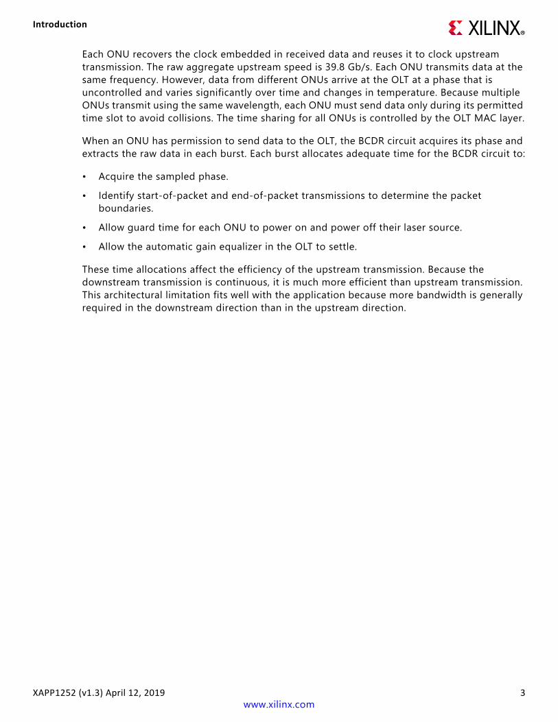
Each ONU recovers the clock embedded in received data and reuses it to clock upstream transmission. The raw aggregate upstream speed is 39.8 Gb/s. Each ONU transmits data at the same frequency. However, data from different ONUs arrive at the OLT at a phase that is uncontrolled and varies significantly over time and changes in temperature. Because multiple ONUs transmit using the same wavelength, each ONU must send data only during its permitted time slot to avoid collisions. The time sharing for all ONUs is controlled by the OLT MAC layer.
When an ONU has permission to send data to the OLT, the BCDR circuit acquires its phase and extracts the raw data in each burst. Each burst allocates adequate time for the BCDR circuit to:
• Acquire the sampled phase.• Identify start-of-packet and end-of-packet transmissions to determine the packet
boundaries.• Allow guard time for each ONU to power on and power off their laser source.• Allow the automatic gain equalizer in the OLT to settle.
These time allocations affect the efficiency of the upstream transmission. Because the downstream transmission is continuous, it is much more efficient than upstream transmission. This architectural limitation fits well with the application because more bandwidth is generally required in the downstream direction than in the upstream direction.

Introduction
XAPP1252 (v1.3) April 12, 2019 4www.xilinx.com
Figure 3 shows the data flow for both downstream and upstream transmissions.
The upstream transmission shows a configuration of phases. Note that all upstream bursts have a preamble, which is required only for upstream transmission. The preamble is a periodic repetition of a 10-bit pattern. This pattern maximizes the statistical information in the preamble to optimize the overall upstream efficiency. The length of the pattern is set by the OLT to a value that allows a BCDR quick-lock circuit to acquire the burst phase.
X-Ref Target - Figure 3
Figure 3: NG-PON2 Downstream and Upstream Transmissions
OLTλ1
λ2
λ3
λ4
OLT
OLT
OLT
Time
λ5
Pack
et P
hase
λ6Phase 1
Packet 1
ONU2
Phase 2
Packet 2
ONU5
Phase 3
Packet 3
ONU6
Phase 2
Packet 2
ONU3
Phase 1
Packet 1
ONU1
Phase 3
Packet 3
ONU4
Downstream
Transmission
Upstream
Transmission
Time
Time
Pack
et P
hase
X22339-022019
Introduction
XAPP1252 (v1.3) April 12, 2019 5www.xilinx.com
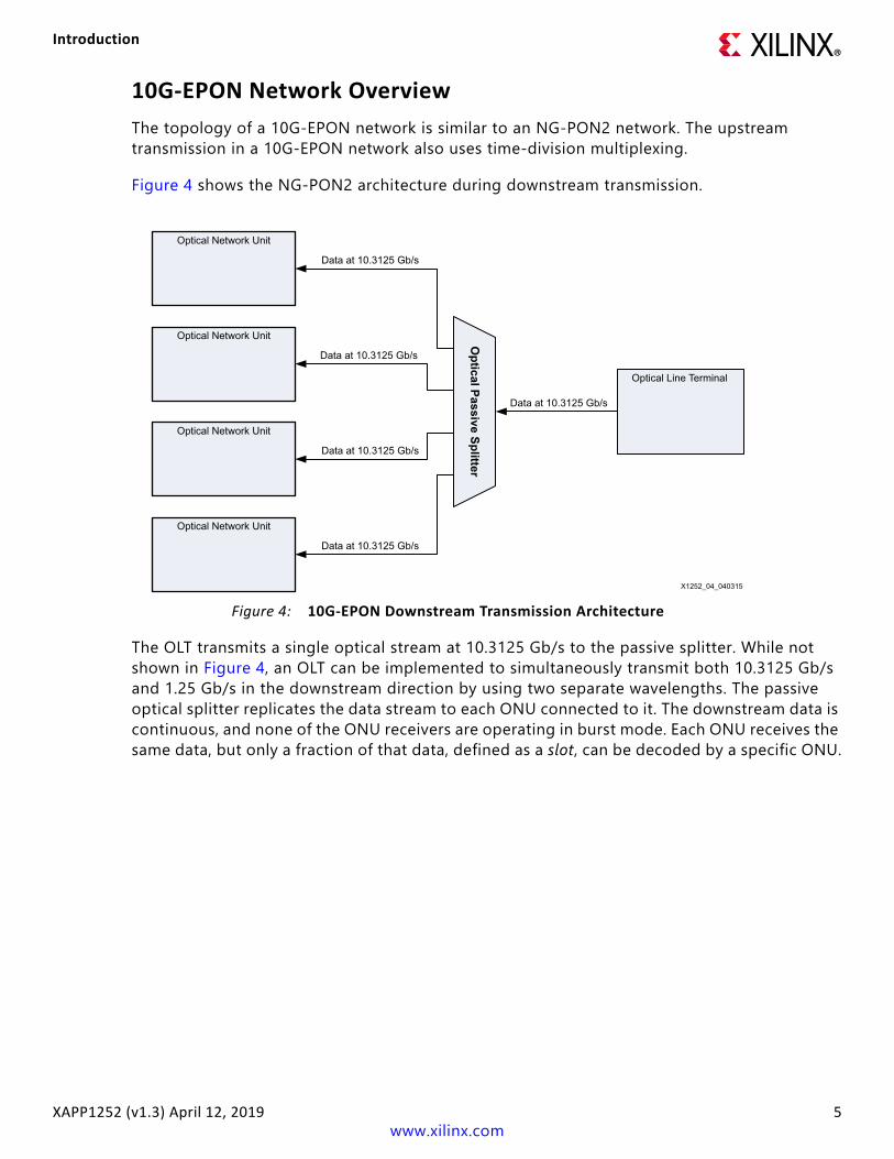
10G-EPON Network OverviewThe topology of a 10G-EPON network is similar to an NG-PON2 network. The upstream transmission in a 10G-EPON network also uses time-division multiplexing.
Figure 4 shows the NG-PON2 architecture during downstream transmission.
The OLT transmits a single optical stream at 10.3125 Gb/s to the passive splitter. While not shown in Figure 4, an OLT can be implemented to simultaneously transmit both 10.3125 Gb/s and 1.25 Gb/s in the downstream direction by using two separate wavelengths. The passive optical splitter replicates the data stream to each ONU connected to it. The downstream data is continuous, and none of the ONU receivers are operating in burst mode. Each ONU receives the same data, but only a fraction of that data, defined as a slot, can be decoded by a specific ONU.
X-Ref Target - Figure 4
Figure 4: 10G-EPON Downstream Transmission ArchitectureX1252_04_040315
Optical Passive Splitter
Data at 10.3125 Gb/s
Data at 10.3125 Gb/s
Data at 10.3125 Gb/s
Data at 10.3125 Gb/s
Optical Line Terminal
Data at 10.3125 Gb/s

Introduction
XAPP1252 (v1.3) April 12, 2019 6www.xilinx.com
Figure 5 shows the 10G-EPON2 architecture for upstream transmission.
Each ONU recovers the clock embedded in received data and reuses it to clock upstream transmission. The raw aggregate upstream speed is 10.3125 Gb/s, assuming all ONUs are transmitting at 10.3125 Gb/s. However, it is possible to also have ONUs transmitting at 1.25 Gb/s simultaneously with ONUs transmitting at 10.3125 Gb/s. Data from different ONUs arrive at the OLT at a phase that is uncontrolled, and varies significantly over time and changes in temperature. Because multiple ONUs can transmit using the same wavelength, each ONU must send data only during its permitted time slot to avoid collisions. The time sharing for all ONUs is controlled by the OLT MAC layer.
When an ONU has permission to send data to the OLT, the BCDR quick-lock circuit acquires its phase and extracts the raw data in each burst. Each burst allocates adequate time for the BCDR circuit to:
• Acquire the sampled phase.• Identify the start-of-packet and end-of-packet to determine the packet boundaries.• Allow guard time for each ONU to power on and power off their laser source.• Allow the automatic gain equalizer in the OLT to settle.
These time allocations affect the efficiency of the upstream transmission. Because the downstream transmission is continuous, it is much more efficient than upstream transmission. This architectural limitation fits well with the application because more bandwidth is generally required in the downstream direction than in the upstream direction.
X-Ref Target - Figure 5
Figure 5: 10G-EPON Upstream Transmission ArchitectureX1252_05_040315
Optical Passive Splitter
Data at 10.3125 Gb/s
Data at 10.3125 Gb/s
Data at 10.3125 Gb/s
Data at 10.3125 Gb/s
Optical Line Terminal
Data at 10.3125 Gb/sBCDR
Circuit Description
XAPP1252 (v1.3) April 12, 2019 7www.xilinx.com
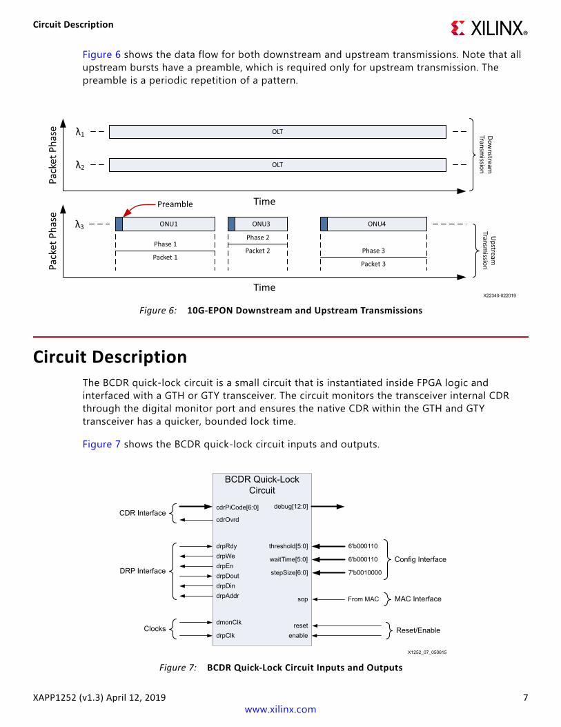
Figure 6 shows the data flow for both downstream and upstream transmissions. Note that all upstream bursts have a preamble, which is required only for upstream transmission. The preamble is a periodic repetition of a pattern.
Circuit DescriptionThe BCDR quick-lock circuit is a small circuit that is instantiated inside FPGA logic and interfaced with a GTH or GTY transceiver. The circuit monitors the transceiver internal CDR through the digital monitor port and ensures the native CDR within the GTH and GTY transceiver has a quicker, bounded lock time.
Figure 7 shows the BCDR quick-lock circuit inputs and outputs.
X-Ref Target - Figure 6
Figure 6: 10G-EPON Downstream and Upstream Transmissions
OLTλ1
λ2 OLT
Time
λ3
Pack
et P
hase
Preamble
Phase 2
Packet 2
ONU3
Phase 1
Packet 1
ONU1
Phase 3
Packet 3
ONU4
Downstream
Transm
issionU
pstream
Transmission
Pack
et P
hase
Time
X22340-022019
X-Ref Target - Figure 7
Figure 7: BCDR Quick-Lock Circuit Inputs and OutputsX1252_07_050615
Config Interface
Clocks
MAC Interface
BCDR Quick-Lock Circuit
dmonClk
drpClk
sop
cdrOvrd
drpAddrdrpDindrpDoutdrpEndrpWedrpRdy
cdrPiCode[6:0]
reset
From MAC
threshold[5:0]
waitTime[5:0]
stepSize[6:0] 7'b0010000
6'b000110
6'b000110
debug[12:0]
enable
CDR Interface
DRP Interface
Reset/Enable

Interfacing the BCDR Quick-Lock Circuit
XAPP1252 (v1.3) April 12, 2019 8www.xilinx.com
Table 1 describes the ports of the BCDR quick-lock circuit IP core.
Interfacing the BCDR Quick-Lock CircuitTo interface the BCDR quick lock-circuit:
1. Generate the GT Wizard IP Core Wrapper using the UltraScale FPGAs Transceivers wizard.2. Instantiate the GT Wrapper and BCDR Quick-Lock Circuit into the PON design.3. Apply proper Timing Constraints and Design Constraints to the design.
Table 1: BCDR Quick-Lock Circuit IP Core PortsPort Direction Clock Domain Description
dmonClk IN N/A DMON clock.
sop IN MAC Clock
Start of burst. Must be asserted immediately after valid preamble bits are known to be arriving at the input of the GTH or GTY transceiver. Care must be taken to ensure this port is never asserted prior to valid preamble bits arriving at the transceiver.
cdrPiCode[6:0] IN DMON clock RX phase code read from the digital monitor port.drpClk IN N/A DRP clock.drpRdy IN drpclk_i
For GTH Transceivers, see the “DRP Ports of GTHE3/4_CHANNEL” table in UltraScale Architecture GTH Transceivers User Guide (UG576) [Ref 1].For GTY Transceivers, see the “DRP Ports of GTYE3/4_CHANNEL” table in UltraScale Architecture GTY Transceivers User Guide (UG578) [Ref 2].
drpWe OUT drpclk_idrpEn OUT drpclk_i
drpDout IN drpclk_idrpDin OUT drpclk_i
drpAddr[8:0] OUT drpclk_i
reset IN AsyncActive-High reset for the BCDR quick lock circuit block. Reset is retimed locally to all internal clock domains. Hold the circuit in reset until the GTH or GTY transceiver completes its reset procedure.
cdrOvrd OUT DMON clock RX CDR override.
threshold[6:0] IN DMON clock Threshold for the difference in phase offset codes that activates the CDR phase adjust.
waitTime[5:0] IN DMON clock Number of cycles that BCDR solution samples DMON output.
stepSize[6:0] IN DMON clock Phase code override offset.enable IN DMON clock Enables the BCDR quick-lock circuit.
debug[12:0] OUT DMON clock Reserved.
Interfacing the BCDR Quick-Lock Circuit
XAPP1252 (v1.3) April 12, 2019 9www.xilinx.com
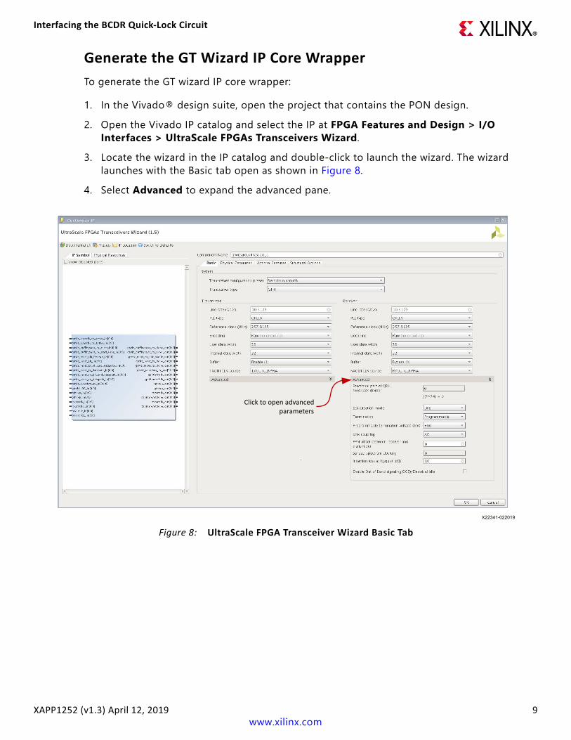
Generate the GT Wizard IP Core WrapperTo generate the GT wizard IP core wrapper:
1. In the Vivado® design suite, open the project that contains the PON design.2. Open the Vivado IP catalog and select the IP at FPGA Features and Design > I/O
Interfaces > UltraScale FPGAs Transceivers Wizard.3. Locate the wizard in the IP catalog and double-click to launch the wizard. The wizard
launches with the Basic tab open as shown in Figure 8.4. Select Advanced to expand the advanced pane.
X-Ref Target - Figure 8
Figure 8: UltraScale FPGA Transceiver Wizard Basic Tab
Click to open advanced parameters
X22341-022019

Interfacing the BCDR Quick-Lock Circuit
XAPP1252 (v1.3) April 12, 2019 10www.xilinx.com
Basic Tab Setup
1. In the Component Name field, Enter a name for your IP core wrapper.2. Select, enter, or verify the values in the remaining fields shown in Figure 9.
IMPORTANT: As shown in Figure 9, both the user data width and the internal data width must be 32 bits wide.
X-Ref Target - Figure 9
Figure 9: Basic Tab Parameters
Select GTH or GTY Depending on Design
Enter 10.3125 for 10G-EPON
Enter 10.3125 for 10G-EPON
Select Bypass
Select DFE
X22342-022019
Interfacing the BCDR Quick-Lock Circuit
XAPP1252 (v1.3) April 12, 2019 11www.xilinx.com
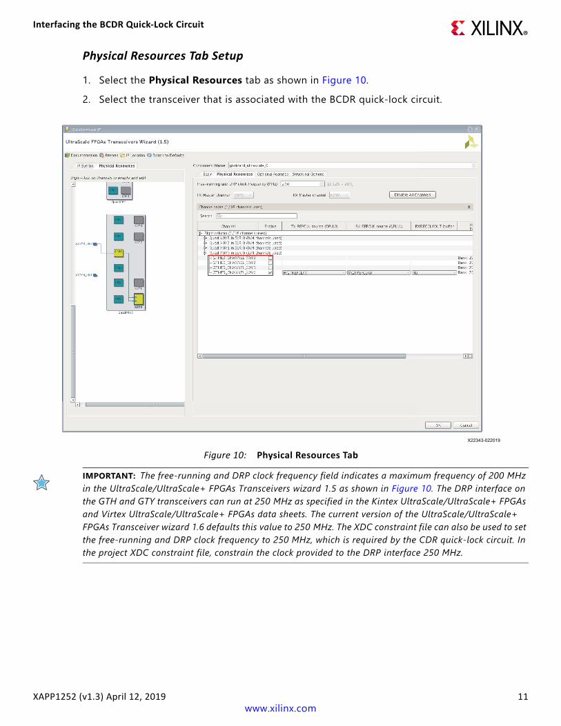
Physical Resources Tab Setup
1. Select the Physical Resources tab as shown in Figure 10.2. Select the transceiver that is associated with the BCDR quick-lock circuit.
IMPORTANT: The free-running and DRP clock frequency field indicates a maximum frequency of 200 MHz in the UltraScale/UltraScale+ FPGAs Transceivers wizard 1.5 as shown in Figure 10. The DRP interface on the GTH and GTY transceivers can run at 250 MHz as specified in the Kintex UltraScale/UltraScale+ FPGAs and Virtex UltraScale/UltraScale+ FPGAs data sheets. The current version of the UltraScale/UltraScale+ FPGAs Transceiver wizard 1.6 defaults this value to 250 MHz. The XDC constraint file can also be used to set the free-running and DRP clock frequency to 250 MHz, which is required by the CDR quick-lock circuit. In the project XDC constraint file, constrain the clock provided to the DRP interface 250 MHz.
X-Ref Target - Figure 10
Figure 10: Physical Resources TabX22343-022019
Interfacing the BCDR Quick-Lock Circuit
XAPP1252 (v1.3) April 12, 2019 12www.xilinx.com
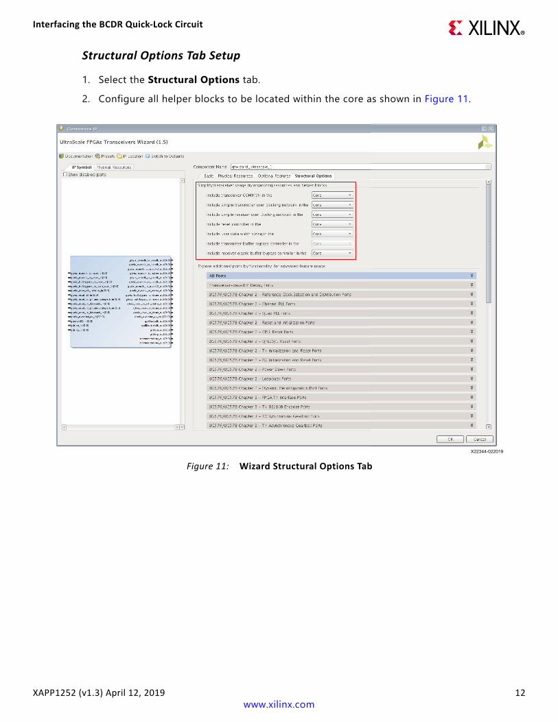
Structural Options Tab Setup
1. Select the Structural Options tab.2. Configure all helper blocks to be located within the core as shown in Figure 11.
X-Ref Target - Figure 11
Figure 11: Wizard Structural Options TabX22344-022019

Interfacing the BCDR Quick-Lock Circuit
XAPP1252 (v1.3) April 12, 2019 13www.xilinx.com
The BCDR quick-lock circuit requires several transceiver ports to be brought out of the GT IP core wrapper. In the Expose additional ports by functionality, for advanced feature usage pane:
1. Locate and click RX Equalizer (DFE and LPM) Ports to expand the RX Equalizer Ports pane.2. Select the checked ports shown Figure 12.
X-Ref Target - Figure 12
Figure 12: RX Equalizer PortsX22345-022019

Interfacing the BCDR Quick-Lock Circuit
XAPP1252 (v1.3) April 12, 2019 14www.xilinx.com
3. Locate and click Dynamic Reconfiguration Ports to expand the Dynamic Reconfiguration Ports.
4. Select the checked ports shown in Figure 13.X-Ref Target - Figure 13
Figure 13: DRP PortsX22346-022019

Interfacing the BCDR Quick-Lock Circuit
XAPP1252 (v1.3) April 12, 2019 15www.xilinx.com
5. Locate and click RX CDR Ports to expand the RX CDR Ports pane.6. Select the ports shown in Figure 14.
X-Ref Target - Figure 14
Figure 14: RX CDR PortsX22347-022019
Interfacing the BCDR Quick-Lock Circuit
XAPP1252 (v1.3) April 12, 2019 16www.xilinx.com
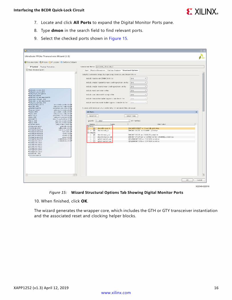
7. Locate and click All Ports to expand the Digital Monitor Ports pane.8. Type dmon in the search field to find relevant ports.9. Select the checked ports shown in Figure 15.
10. When finished, click OK.
The wizard generates the wrapper core, which includes the GTH or GTY transceiver instantiation and the associated reset and clocking helper blocks.
X-Ref Target - Figure 15
Figure 15: Wizard Structural Options Tab Showing Digital Monitor PortsX22348-022019

Interfacing the BCDR Quick-Lock Circuit
XAPP1252 (v1.3) April 12, 2019 17www.xilinx.com
Instantiate the GT Wrapper and BCDR Quick-Lock CircuitEach GTH or GTY transceiver used in a PON application requires an instance of the GT wizard IP core wrapper and an instance of the BCDR quick-lock circuit. Connect the exposed ports on the GT wizard IP core wrapper and make the connections with the BCDR quick-lock circuit as shown in Figure 16 and Figure 17. While the BCDR quick-lock circuit is enabled, the DRP interface on the GTH or GTY transceiver must only be allowed to communicate with the BCDR quick-lock circuit.
X-Ref Target - Figure 16
Figure 16: UltraScale FPGA BCDR Quick-Lock Circuit and Core Wrapper
BUFGdmonitorout_out[16]
dmonitorclk_in
GT Wizard IP Core Wrapper Instance
UltraScale BCDRQuick-Lock Circuit Instance
dmonClk
drpClk
250 MHz
drpclk_in
drpaddr_in
drpdi_in
drpdo_out
drpen_in
drpwe_in
rxcdrovrden_in
sop
cdrOvrd
drpAddr
drpDin
drpDout
drpEn
drpWe
drprdy_out drpRdy
dmonitorout_out[6:0] cdrPiCode[6:0]
reset
From MAC
rxdfelfovrden_inrxdfeagcovrden_in
1
rxdfetap2ovrden_inrxdfetap3ovrden_inrxdfetap4ovrden_inrxdfetap5ovrden_inrxdfetap6ovrden_inrxdfetap7ovrden_inrxdfetap8ovrden_inrxdfetap9ovrden_inrxdfetap10ovrden_inrxdfetap11ovrden_inrxdfetap12ovrden_inrxdfetap13ovrden_inrxdfetap14ovrden_inrxdfetap15ovrden_in
threshold[6:0]
waitTime[5:0]
stepSize[6:0] 7'b0010000
6'b000110
7'b0000110
BUFG
debug[12:0]
enable
X22412-022819

Interfacing the BCDR Quick-Lock Circuit
XAPP1252 (v1.3) April 12, 2019 18www.xilinx.com
1. Add the BCDR_QuickLock.dcp file to the project.
The design checkpoint (DCP) file provided with this application note provides the BCDR quick-lock circuit as a precompiled file, BCDR_QuickLock.dcp. To add this file to the project as a design source:
a. In the Flow Navigator pane, open Project Manager and select Add Sources.
X-Ref Target - Figure 17
Figure 17: UltraScale+ FPGA BCDR Quick-Lock Circuit and Core Wrapper
GT Wizard IP CoreWrapper Instance
rxdfetap15ovrden_in
dmonitorout_out[6:0]
rxcdrovrden_in
dmonitoroutclk
dmonitorclk_in
drprdy_out
drpwe_in
drpen_in
drpdi_in
drpaddr_in
drpdo_out
drpclk_in
rxdfetap14ovrden_inrxdfetap13ovrden_inrxdfetap12ovrden_inrxdfetap11ovrden_inrxdfetap10ovrden_inrxdfetap9ovrden_inrxdfetap8ovrden_inrxdfetap7ovrden_inrxdfetap6ovrden_inrxdfetap5ovrden_inrxdfetap4ovrden_inrxdfetap3ovrden_inrxdfetap2ovrden_inrxdfeagcovrden_inrxdfelfovrden_in1
UltraScale+ BCDR Quick-Lock Circuit Instance
cdrPiCode[6:0] debug[12:0]
threshold[6:0]
drpRdy
drpWe
drpEn
drpDin
drpAddr
drpDout
drpClk
cdrOvrd
BUFG250 MHz
BUFG_GTdmonClk
waitTime[5:0]
stepSize[5:0]
sop
reset
enable
7'b0000110
6'b000110
7'b0010000
From MAC
X18036-022819
X-Ref Target - Figure 18
Figure 18: Add SourcesX22349-022019

Interfacing the BCDR Quick-Lock Circuit
XAPP1252 (v1.3) April 12, 2019 19www.xilinx.com
b. Select Add or create design sources.
Figure 20 shows the BCDR_QuickLock.dcp file added to the design sources hierarchy in the project.
X-Ref Target - Figure 19
Figure 19: Add BCDR_QuickLock.dcp to Design SourcesX22350-022019
X-Ref Target - Figure 20
Figure 20: BCDR_QuickLock.dcp Added to Design SourcesX22351-022019
Interfacing the BCDR Quick-Lock Circuit
XAPP1252 (v1.3) April 12, 2019 20www.xilinx.com
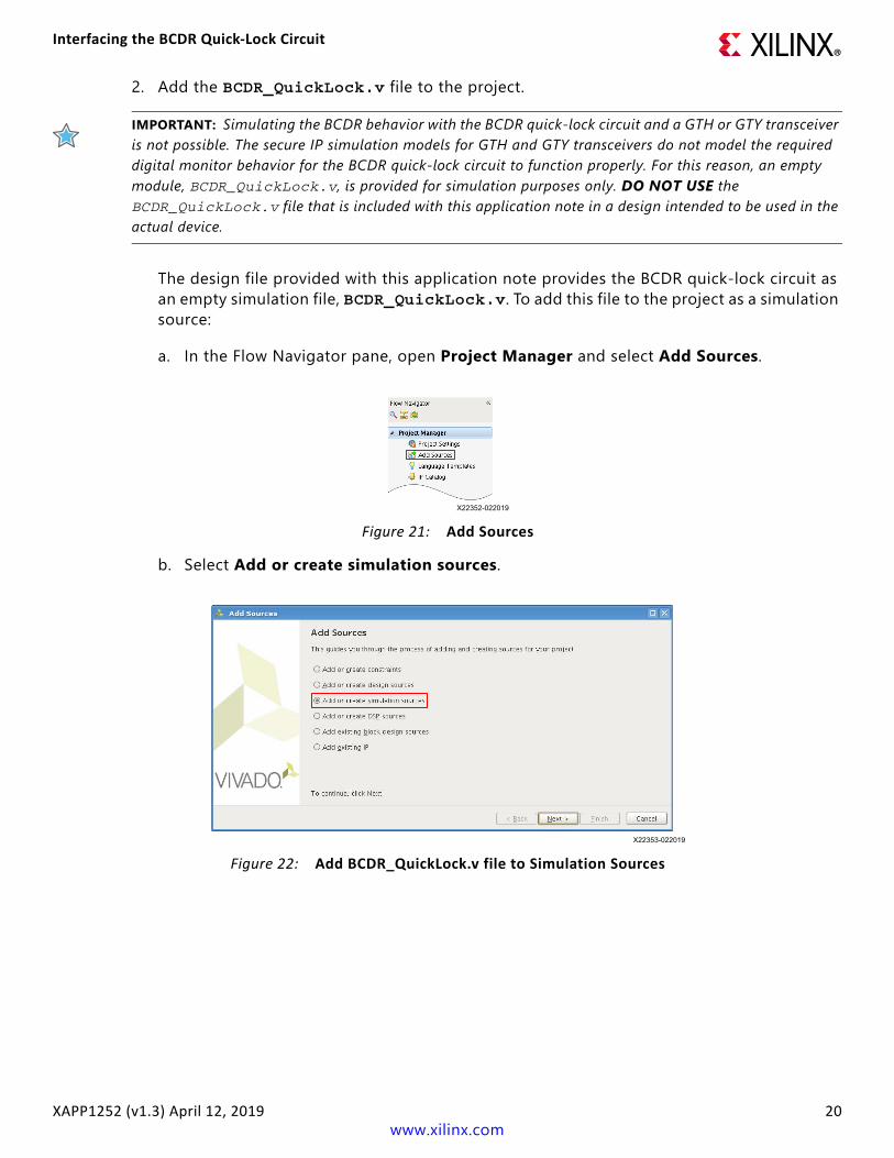
2. Add the BCDR_QuickLock.v file to the project.
IMPORTANT: Simulating the BCDR behavior with the BCDR quick-lock circuit and a GTH or GTY transceiver is not possible. The secure IP simulation models for GTH and GTY transceivers do not model the required digital monitor behavior for the BCDR quick-lock circuit to function properly. For this reason, an empty module, BCDR_QuickLock.v, is provided for simulation purposes only. DO NOT USE the BCDR_QuickLock.v file that is included with this application note in a design intended to be used in the actual device.
The design file provided with this application note provides the BCDR quick-lock circuit as an empty simulation file, BCDR_QuickLock.v. To add this file to the project as a simulation source:
a. In the Flow Navigator pane, open Project Manager and select Add Sources.
b. Select Add or create simulation sources.
X-Ref Target - Figure 21
Figure 21: Add SourcesX22352-022019
X-Ref Target - Figure 22
Figure 22: Add BCDR_QuickLock.v file to Simulation SourcesX22353-022019

Interfacing the BCDR Quick-Lock Circuit
XAPP1252 (v1.3) April 12, 2019 21www.xilinx.com
Figure 23 shows the BCDR_QuickLock.v file added to the simulation sources hierarchy in the project.
Design ConstraintsSeveral design constraints must be considered for this design and added to the Xilinx design constraints (XDC) file.
GTH and GTY Transceiver Attributes
To enable the digital monitor and configure the CDR for UltraScale FPGA GTH and GTY transceivers, use set_property commands in the project XDC file to override the attributes listed in Table 2 and Table 3.
X-Ref Target - Figure 23
Figure 23: BCDR_QuickLook.v File Added to Simulation SourcesX22354-022019
Table 2: UltraScale FPGA GTH Transceiver Attribute Settings to be Overridden by XDC ConstraintsGTH Transceiver Attribute Value
ADAPT_CFG1 16'b0001000000000000
DMONITOR_CFG1 8'b00000001
RXCDR_CFG0 16'b0010000000000000
RXCDR_CFG216'b0000010101000110 (10G-EPON preamble)16'b0000010101010110 (NG-PON2 preamble)
Interfacing the BCDR Quick-Lock Circuit
XAPP1252 (v1.3) April 12, 2019 22www.xilinx.com
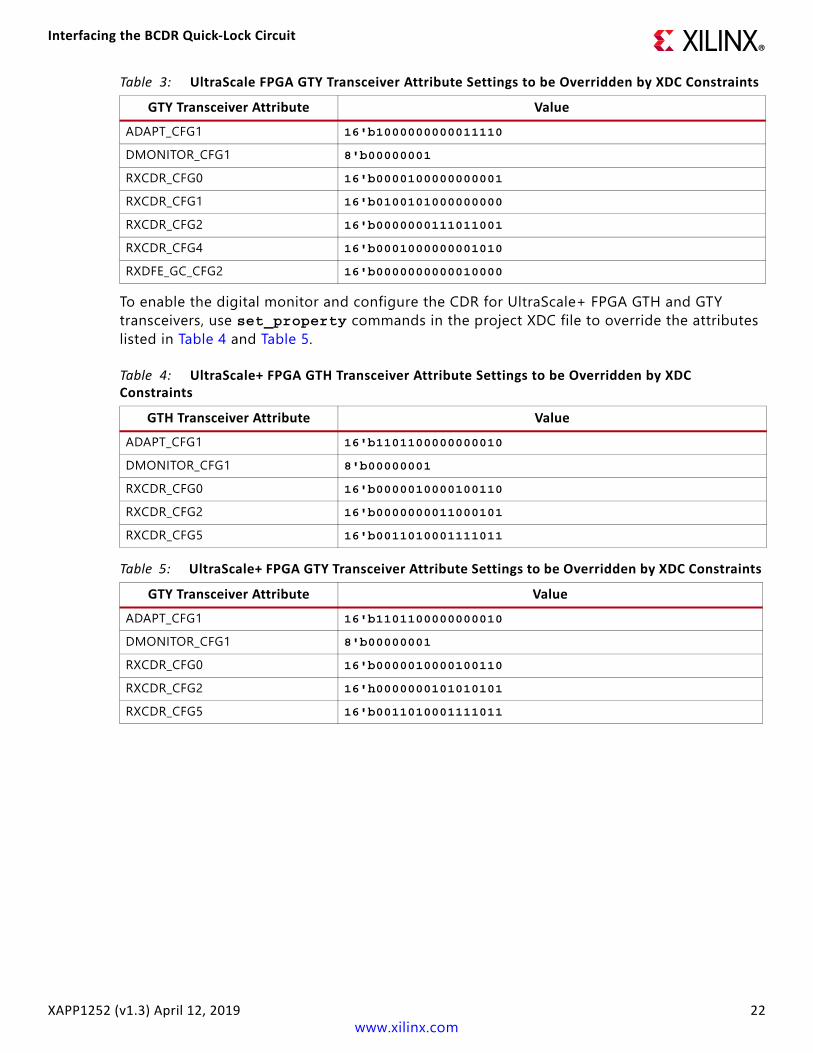
To enable the digital monitor and configure the CDR for UltraScale+ FPGA GTH and GTY transceivers, use set_property commands in the project XDC file to override the attributes listed in Table 4 and Table 5.
Table 3: UltraScale FPGA GTY Transceiver Attribute Settings to be Overridden by XDC ConstraintsGTY Transceiver Attribute Value
ADAPT_CFG1 16'b1000000000011110
DMONITOR_CFG1 8'b00000001
RXCDR_CFG0 16'b0000100000000001
RXCDR_CFG1 16'b0100101000000000
RXCDR_CFG2 16'b0000000111011001
RXCDR_CFG4 16'b0001000000001010
RXDFE_GC_CFG2 16'b0000000000010000
Table 4: UltraScale+ FPGA GTH Transceiver Attribute Settings to be Overridden by XDC Constraints
GTH Transceiver Attribute ValueADAPT_CFG1 16'b1101100000000010
DMONITOR_CFG1 8'b00000001
RXCDR_CFG0 16'b0000010000100110
RXCDR_CFG2 16'b0000000011000101
RXCDR_CFG5 16'b0011010001111011
Table 5: UltraScale+ FPGA GTY Transceiver Attribute Settings to be Overridden by XDC ConstraintsGTY Transceiver Attribute Value
ADAPT_CFG1 16'b1101100000000010
DMONITOR_CFG1 8'b00000001
RXCDR_CFG0 16'b0000010000100110
RXCDR_CFG2 16'h0000000101010101
RXCDR_CFG5 16'b0011010001111011

Interfacing the BCDR Quick-Lock Circuit
XAPP1252 (v1.3) April 12, 2019 23www.xilinx.com
An example set_property command is shown here. The specific hierarchical path is an example only:
set_property ADAPT_CFG1 16'b1000000000011110 [get_cells -hierarchical -filter{NAME =~ *gen_channel_container[0].*gen_gthe3_channel_inst[0].GTHE3_CHANNEL_PRIM_INST}]
Location Constraints
For UltraScale FPGAs, use the set_property LOC to constrain the BUFG used to buffer the digital monitor clock to a BUFG that is located nearest the transceiver.
An example location constraint is shown here. The specific BUFG location and instance name are examples only:
set_property LOC BUFGCE_X1Y50 [get_cells ch0_dmon_bufg]
For UltraScale+ FPGAs, the tool automatically picks the location of the BUFG_GT used to buffer the digital monitor clock to the same clock region as the transceiver. There is no need to manually constrain the BUFG_GT.
Timing Constraints
Timing constraints must be applied to the clocks listed in Table 6.
An example timing constraint for the digital monitor clock is shown here. The specific clock name, period value and BUFG instance name are examples only:
create_clock -name CH0_DMONCLK -period 3.103 [get_pins ch0_dmon_bufg/O]
Table 6: Required Clock Timing ConstraintsClock Required Timing Constraint
Digital Monitor clock Line rate/GT internal data widthGT reference clock Reference clock frequencyDRP clock 250 MHz
Reference Design
XAPP1252 (v1.3) April 12, 2019 24www.xilinx.com
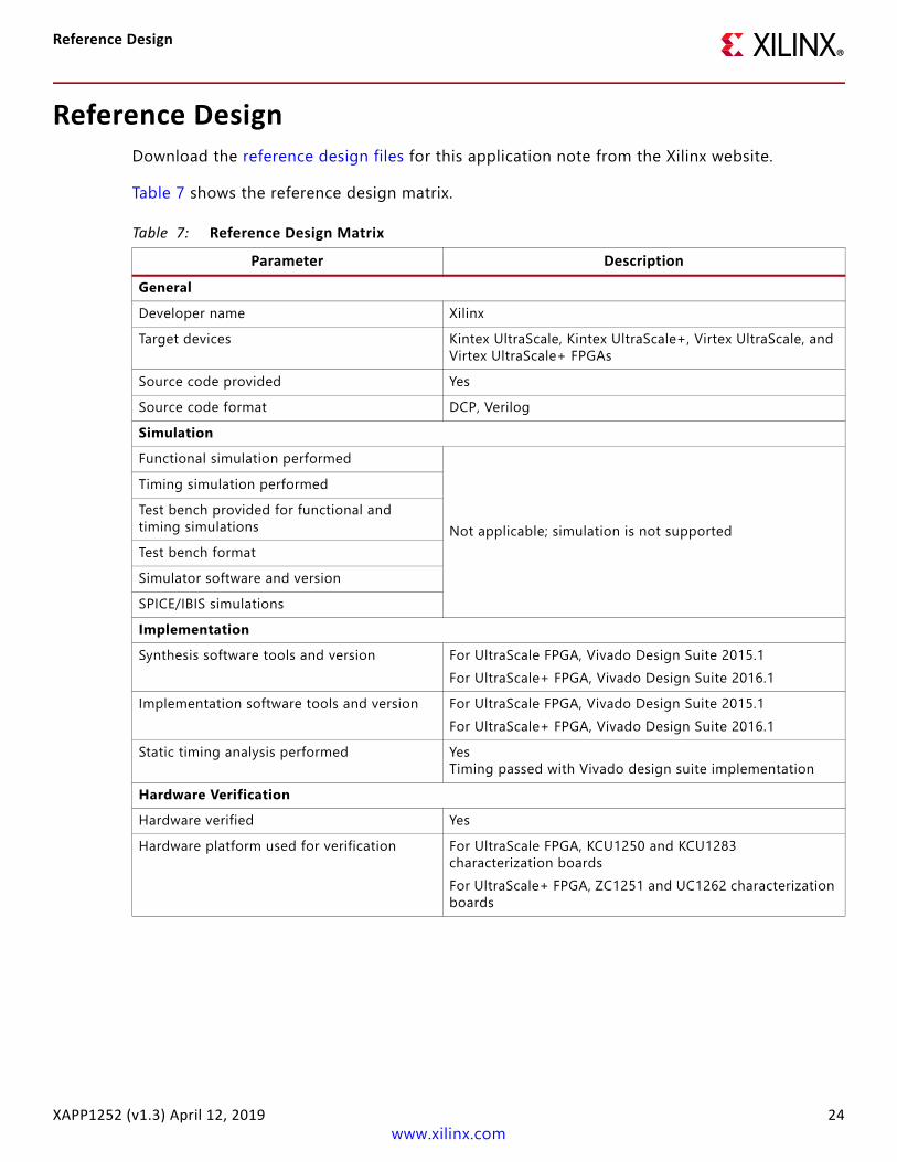
Reference DesignDownload the reference design files for this application note from the Xilinx website.
Table 7 shows the reference design matrix.
Table 7: Reference Design MatrixParameter Description
GeneralDeveloper name XilinxTarget devices Kintex UltraScale, Kintex UltraScale+, Virtex UltraScale, and
Virtex UltraScale+ FPGAsSource code provided YesSource code format DCP, VerilogSimulationFunctional simulation performed
Not applicable; simulation is not supported
Timing simulation performedTest bench provided for functional andtiming simulationsTest bench formatSimulator software and versionSPICE/IBIS simulationsImplementationSynthesis software tools and version For UltraScale FPGA, Vivado Design Suite 2015.1
For UltraScale+ FPGA, Vivado Design Suite 2016.1Implementation software tools and version For UltraScale FPGA, Vivado Design Suite 2015.1
For UltraScale+ FPGA, Vivado Design Suite 2016.1Static timing analysis performed Yes
Timing passed with Vivado design suite implementationHardware VerificationHardware verified YesHardware platform used for verification For UltraScale FPGA, KCU1250 and KCU1283
characterization boardsFor UltraScale+ FPGA, ZC1251 and UC1262 characterization boards
References
XAPP1252 (v1.3) April 12, 2019 25www.xilinx.com
ConclusionThis application note described how to enhance the performance of the CDR circuit used by the GTH and GTY transceivers in UltraScale devices. A BCDR quick-start circuit was implemented for use in NG-PON2 and 10G-EPON passive optical network applications where fast and bounded lock times are required.
ReferencesThis application note uses the following references:
1. UltraScale Architecture GTH Transceivers User Guide (UG576)2. UltraScale Architecture GTY Transceivers User Guide (UG578)3. UltraScale FPGAs Transceivers Wizard 1.5 LogiCORE IP Product Guide (PG182)4. Fractional Burst Clock Data Recovery for XG-PON Applications (XAPP1083)5. Ethernet Standard, IEEE Std 802.3av (www.ieee802.org/3/)6. NG-PON2 Standard (ITU-T G.989.3) (www.itu.int/itu-t/workprog/wp_item.aspx?isn=9119)
Revision HistoryThe following table shows the revision history for this document.
Date Version Revision04/12/2019 1.3 Revised threshold port in Figure 16 and Figure 17.02/20/2019 1.2 Added an Important note below Figure 9 on page 10. Updated Figure 17.11/17/2016 1.1 Added UltraScale+ FPGA information throughout.06/17/2015 1.0 Initial Xilinx release.

Please Read: Important Legal Notices
XAPP1252 (v1.3) April 12, 2019 26www.xilinx.com
Please Read: Important Legal NoticesThe information disclosed to you hereunder (the “Materials”) is provided solely for the selection and use of Xilinx products. To the maximum extent permitted by applicable law: (1) Materials are made available "AS IS" and with all faults, Xilinx hereby DISCLAIMS ALL WARRANTIES AND CONDITIONS, EXPRESS, IMPLIED, OR STATUTORY, INCLUDING BUT NOT LIMITED TO WARRANTIES OF MERCHANTABILITY, NON-INFRINGEMENT, OR FITNESS FOR ANY PARTICULAR PURPOSE; and (2) Xilinx shall not be liable (whether in contract or tort, including negligence, or under any other theory of liability) for any loss or damage of any kind or nature related to, arising under, or in connection with, the Materials (including your use of the Materials), including for any direct, indirect, special, incidental, or consequential loss or damage (including loss of data, profits, goodwill, or any type of loss or damage suffered as a result of any action brought by a third party) even if such damage or loss was reasonably foreseeable or Xilinx had been advised of the possibility of the same. Xilinx assumes no obligation to correct any errors contained in the Materials or to notify you of updates to the Materials or to product specifications. You may not reproduce, modify, distribute, or publicly display the Materials without prior written consent. Certain products are subject to the terms and conditions of Xilinx’s limited warranty, please refer to Xilinx’s Terms of Sale which can be viewed at https://www.xilinx.com/legal.htm#tos; IP cores may be subject to warranty and support terms contained in a license issued to you by Xilinx. Xilinx products are not designed or intended to be fail-safe or for use in any application requiring fail-safe performance; you assume sole risk and liability for use of Xilinx products in such critical applications, please refer to Xilinx’s Terms of Sale which can be viewed at https://www.xilinx.com/legal.htm#tos.Automotive Applications DisclaimerAUTOMOTIVE PRODUCTS (IDENTIFIED AS "XA" IN THE PART NUMBER) ARE NOT WARRANTED FOR USE IN THE DEPLOYMENT OF AIRBAGS OR FOR USE IN APPLICATIONS THAT AFFECT CONTROL OF A VEHICLE ("SAFETY APPLICATION") UNLESS THERE IS A SAFETY CONCEPT OR REDUNDANCY FEATURE CONSISTENT WITH THE ISO 26262 AUTOMOTIVE SAFETY STANDARD ("SAFETY DESIGN"). CUSTOMER SHALL, PRIOR TO USING OR DISTRIBUTING ANY SYSTEMS THAT INCORPORATE PRODUCTS, THOROUGHLY TEST SUCH SYSTEMS FOR SAFETY PURPOSES. USE OF PRODUCTS IN A SAFETY APPLICATION WITHOUT A SAFETY DESIGN IS FULLY AT THE RISK OF CUSTOMER, SUBJECT ONLY TO APPLICABLE LAWS AND REGULATIONS GOVERNING LIMITATIONS ON PRODUCT LIABILITY.© Copyright 2015–2019 Xilinx, Inc. Xilinx, the Xilinx logo, Artix, ISE, Kintex, Spartan, Virtex, Vivado, Zynq, and other designated brands included herein are trademarks of Xilinx in the United States and other countries. All other trademarks are the property of their respective owners.