Embed Size (px)
Citation preview

IEEE TRANSACTIONS ON COMPUTER-AIDED DESIGN OF INTEGRATED CIRCUITS AND SYSTEMS, VOL. 18, NO. 11, NOVEMBER 1999 1633
Buffer Insertion for Noise and Delay OptimizationCharles J. Alpert,Member, IEEE, Anirudh Devgan,Member, IEEE, and Stephen T. Quay
Abstract—Interconnect-driven optimization is an increasinglyimportant step in high-performance design. Algorithms for bufferinsertion have been successfully utilized to reduce delay in globalinterconnect paths; however, existing techniques only optimizedelay and timing slack. With the continually increasing ratioof coupling capacitance to total capacitance and the use ofaggressive dynamic logic circuit families, noise analysis andavoidance is becoming a major design bottleneck. Hence, timingand noise must be simultaneously optimized to achieve maximumperformance. This paper presents comprehensive buffer insertiontechniques for noise and delay optimization. Three algorithmsare presented, the first for noise avoidance for single sink trees,the second for avoidance for multiple sink trees, and the last forsimultaneous noise and delay optimization. We prove the optimal-ity of each algorithm (under various assumptions) and presentother theoretical results as well. We ran experiments on a high-performance microprocessor design and show that our approachfixes all noise violations. Our approach was separately verified bya detailed, simulation-based noise analysis tool. Further, we showthat optimizing delay alone cannot fix all of the noise violationsand that the performance penalty induced by optimizing bothdelay and noise as opposed to only delay is less than 2%.
Index Terms—Buffer insertion, interconnect-synthesis, noiseanalysis, routing, Steiner-tree.
I. INTRODUCTION
PERFORMANCE optimization has always been a criticalstep in the design of integrated circuits. Process tech-
nology scaling into the deep submicron regime has madeinterconnect performance more dominant than transistor andlogic performance. With the continued scaling of processtechnology, the resistance per unit length of the interconnectcontinues to increase, the capacitance per unit length remainsroughly constant and transistor or logic delay continues todecrease. This trend has led to interconnect delay been moredominant than logic delay. Process technology options, such asuse of copper wires instead of aluminum can only provide tem-porary relief. The trend of increasing interconnect dominanceis expected to continue.
Interconnect-driven timing optimization techniques, suchas wire sizing, buffer insertion and gate sizing have gainedwidespread acceptance in deep submicron design (see Conget al. [7] for an excellent survey on layout optimizationand interconnect synthesis). In particular, buffer insertiontechniques have been successful in reducing interconnectdelay. To the first order, interconnect delay is proportional
Manuscript received December 24, 1998; revised July 27, 1999. This paperwas recommended by Associate Editor M. Pedram.
C. J. Alpert is with the IBM Austin Research Laboratory, Austin, TX 78758USA (e-mail: [email protected]).
A. Devgan and S. T. Quay are with the IBM Server Group, Austin, TX78758 USA (e-mail: [email protected]; [email protected]).
Publisher Item Identifier S 0278-0070(99)09466-X.
to the square of the length of the wire. Inserting bufferseffectively divides the wire into smaller segments, whichmakes the delay almost linear in terms of interconnect length(plus the buffer delays). Additional advantages of bufferinsertion will make this optimization even more pervasive asthe ratio of device to interconnect delay continues to decrease.
Several works have studied the delay-driven buffer insertionproblem. Closed formed solutions have been proposed byAlpert and Devgan [1], Bakoglu [2], Chu and Wong [5], andDhar and Franklin [9], all of which find exact solutions (underdifferent assumptions) for inserting buffers on a two-pin net.Approaches which simultaneously construct a routing tree andinsert buffers have been proposed by Kanget al. [13], Lilliset al. [19], and Okamoto and Cong [23]; Bermanet al. [3]showed this problem is NP-complete. The works of Kannanet al. [14] and Lin and Marek-Sadowska [20] insert bufferson a tree by iteratively finding the best location for a singlebuffer. Finally, a number of works [1], [17]–[19], [23] canbe classified as extensions and variants to Van Ginneken’sdynamic programming algorithm [31] which finds the optimalbuffer placement under the Elmore delay model [10]. Lilliset al. [18] extended the algorithm to simultaneously performwire sizing and buffer insertion using a buffer library thatcontains both inverting and noninverting buffers. In addition,they show how to integrate skew into the gate delay model andoptimize a power function (e.g., the total number of buffers),all while retaining optimality. Later, Lillis [17] extended thiswork to handle nets with multiple sources. Alpert and Devgan[1] proposed a wire segmenting preprocessing algorithm tohandle the one buffer per wire limitation of Van Ginneken’salgorithm, which results in a smooth tradeoff between solutionquality and run time.
Although timing optimization has always been critical inthe design process, present day design techniques and processtechnologies are making noise analysis and avoidance asimportant, or in some cases, even more important than timinganalysis and optimization. The shrinking of minimum dis-tance between adjacent wires has caused an increase in thecoupling capacitance of a net to its neighbors. Furthermore,a wire’s thickness is typically greater than its width, whichhas increased the ratio of coupling to total capacitance. Alarge coupling capacitance can cause a switching net to in-duce significant noise onto a neighboring net, resulting in anincorrect functional response. Further, the widespread use offast dynamic logic circuits and its derivative logic families hasmade noise avoidance and analysis even more critical sincethese logic families are more susceptible to noise failure.
It is no longer sufficient or even acceptable to optimize onlyfor delay. Noise avoidance techniques must become an integral
0278–0070/99$10.00 1999 IEEE

1634 IEEE TRANSACTIONS ON COMPUTER-AIDED DESIGN OF INTEGRATED CIRCUITS AND SYSTEMS, VOL. 18, NO. 11, NOVEMBER 1999
(a)
(b)
Fig. 1. The noise effect on a victim net: (a) without a buffer and (b) witha buffer.
part of the performance optimization environment. Bufferinsertion provides a suitable environment for simultaneousoptimization of timing and noise.
Consider the circuit shown in Fig. 1. The amount of cou-pling capacitance from one net to another is proportional to thedistance that the two nets run parallel to each other. Fig. 1(a)illustrates the noise effects that the aggressor net (top) canhave on the victim net (bottom). The coupling capacitancemay cause an input signal on the aggressor net to induce anoise pulse on the victim net. If the resulting noise is greaterthan the tolerable noise margin (NM) of the sink, then anelectrical fault results. Fig. 1(b) shows how inserting a buffercan distribute the capacitive coupling between the two newlycreated wires, resulting in a smaller noise pulse on the inputof the inserted buffer than the pulse in Fig. 1(a). Since thebuffer is a restoring logic gate, ideally no noise is propagatedto its output (if the noise induced on its input is less than thetolerable noise margin). The second wire will also receive asmaller noise pulse, and if the amplitude of this noise pulseis lower the sink’s noise margin, the circuit will functioncorrectly. Further, if the wire is long enough, insertion of thebuffer will also reduce the total source to sink delay.
Various noise analysis and avoidance techniques have beenproposed over the last few years [4], [12], [24], [28], [29], [32].Circuit simulation techniques, such as SPICE [22], can also beused for noise estimation. When the problem can be modeledas a linear circuit (which it generally can be for most couplednoise problems), specialized linear model reduction techniques(such as rapid interconnect circuit evaluation (RICE) [27] orasymptotic waveform evaluation (AWE) [25]) are typicallyapplied [10], [26]. For linear circuits, model reduction ispreferred to circuit simulation due to the computational costsavings; however, the cost may still be prohibitive. The run-time concurrents are even more critical if noise analysis isto be performed within a physical design system, such as aglobal router. Hence, model reduction and circuit simulationare not suitable for these applications. Geometric noise models,e.g., based on geometric distances between wires, are compu-tationally efficient enough to be used within a physical designsystem (such as a global router). However, these models arenot accurate since they ignore the electrical properties of thecircuit.
Simplified electrical noise metrics are particularly amenablefor use within a physical design optimization tool since theycan be efficient and accurate. Vittal and Marek-Sadowska[32] proposed a noise model for crosstalk and showed how
to reduce crosstalk during channel routing. The authors of[32] model a coupled network as a simplified RC circuitin which the capacitances for the victim line, coupling, andthe aggressor line are modeled as lumped capacitances, andthe gates are modeled by linear resistors. They then deriveanalytical expressions for noise from the resultant RC circuit.However, the Vittal and Marek-Sadowska do not consider theresistances for the victim and aggressor lines. Stohret al. [29]represent the victim and aggressor net as simplified T modelscircuits and compute analytical noise expressions similar thatare similar to those in [32].
The recently proposed noise metric of Devgan [8] efficientlycomputes coupled noise while considering circuit effects suchas input slew rate, line resistances, and coupling capacitances.A nice feature of the metric is that its computational com-plexity, structure, and incremental nature is the same as thefamous Elmore delay metric (see Section II-B), which makeit particularly amenable for noise avoidance. Further, like theElmore metric for delay, the noise metric is a provable upperbound on coupled noise. Other advantages of the noise metricinclude the ability to incorporate multiple aggressor nets andhandle general victim and aggressor net topologies. For thesereasons, we adopt the Devgan noise metric in this work.
A disadvantage of the Devgan metric is that it becomes morepessimistic as the ratio of the aggressor net’s transition time(at the output of the driver) to its delay decreases. However,cases in which this ratio becomes very small are rare sincea long net delay generally corresponds to a large load onthe driver, which in turn causes a slower transition time. Themetric also does not consider the duration of the noise pulse.In general, the noise margin of a gate is dependent on boththe peak noise amplitude and the noise pulse width. However,when considering failure at a gate, peak amplitude dominatespulse width. In other words, the gate is much more sensitiveto a change in peak amplitude than a change in pulse width.Consequently, the induced noise can be approximated by thepeak noise amplitude, especially when the noise metric is anupper bound. In practice, we observe that the Devgan metricprovides a computationally efficient and sufficiently accuratenoise estimate, as illustrated through the realistic industrialexamples studied in Section V.
The following contributions are made in the paper.
• We propose a formula for the maximum length of a wiresuch that no noise violation is induced. We prove thatany buffer insertion algorithm that optimizes only delayis insufficient for fixing noise violations.
• We present two algorithms for optimal buffer insertionfor noise avoidance. The first is an optimal linear-timealgorithm for two-pin nets, and the second is an optimalquadratic-time algorithm for multipin nets.
• We present a third algorithm for minimizing the maxi-mum source to sink delay such that all noise constraintsare satisfied. The algorithm is optimal under the conditionthat the buffer library contains a single buffer type.
• Experiments with an industrial noise analysis tool showthat our algorithm eliminates all noise violations for aset of 500 nets from a modern microprocessor design,while optimizing for delay alone does not eliminate

ALPERT et al.: BUFFER INSERTION FOR NOISE AND DELAY OPTIMIZATION 1635
all violations. Further, the average delay penalty forsimultaneously optimizing noise and delay compared tooptimizing delay alone is only 2%.
The rest of our paper is as follows. Section II discussespresents notation, a review of Devgan’s noise metric [8], andthe problem formulations that we study. Section III presentsoptimal buffer insertion algorithms for noise avoidance, andSection IV presents an optimal algorithm for simultaneouslyoptimizing noise and delay. Section V presents experimentalresults, and we conclude in Section VI.
II. PRELIMINARIES
We assume that the input routing tree topology is fixed orthat a Steiner estimation has been computed for the given net.A routing tree contains a set of wires anda set of nodes where is the uniquesourcenode, is the set of sink nodes, and is the setof internal nodes. A wire with length is an orderedpair of nodes in which the signal propagates from
to . Each node has a uniqueparent wire. The tree is assumed to bebinary, i.e., each node
can have at most two children.1 Let the left and right childrenof be denoted by and , respectively. Weassume that if has only one child, then it is . Thepath from node to , denoted by , is an orderedsubset of wires of
. A buffer library is also given.A buffer insertion solution is a mapping
which either assigns a buffer or no buffer, denotedby , to each internal node of .2 Let
denote the number of internal nodeswith inserted buffers from solution . For sufficiently longwires in which multiple buffers may need to be inserted,wires should first be segmented (e.g., as in [1]) to createas many internal nodes as necessary to form a reasonableset of potential locations for buffer insertion.3 Assigningbuffers to induces nets, and hence subtrees,each with no internally placed buffers. For each , let
, the subtree rootedat , be the maximal subtree of such that is the sourceand contains no internal buffers. Observe that if ,
contains only one node.
A. Delay Optimization
As in [1], [18], [23], and [31], we adopt the Elmore delay
1In general, a routed Steiner topology will never have more than threechildren. Such a topology is converted into a binary tree by considering eachnode v with three children, saya, b, and c. A dummy infeasible nodewis inserted and two of the children, saya and b, are picked to be childrenof w. Node v now has two children,c and w, and wire (v; w) has zerolength. Which pair of nodes are chosen to be children ofw does not affectthe solutions returned by any of the algorithms presented.
2A buffer placed on an internal node with degreed is interpreted as havingone input, one output, andd� 1 fanouts.
3Note that our algorithms are independent of the wire segmenting algorithmused. Solution quality increases as the number of internal nodes increases,albeit at the expense of runtime. Indeed, it may be appropriate to develop anew wire segmenting algorithm for the particular formulations we address.
model4 [10] for interconnect delays and a linear model for gatedelays. For each gate, let denote the input capacitance,
the intrinsic resistance and the intrinsic delay of . Letand , respectively, denote the lumped capacitance and
resistance for each wire . The capacitive load seen atnode is the total lumped capacitance of , i.e.,
(1)
The Elmore delay for a wire is given by
(2)
The delay through a gate is given by
(3)
If , , then . The total delayfrom to is given by
(4)Each sink has a given required arrival time ,
and we assume that the input signal arrives at the source nodeat time zero. The condition
(5)
must hold for the circuit to meet its timing require-ments. We define theslack for every as
where is the setof all sinks that are downstream from, i.e., is an ancestorof all sinks in . This definition differs slightly from thetraditional definition of slack, but one can see that they areactually the same if is viewed as the root of the tree. Observethat the conditions in (5) holds if and only if .
B. Noise Avoidance
In [8], Devgan proposed a coupled noise estimation metricthat is similar in spirit to Elmore delay. The noise metric isan upper bound for RC and overdamped RLC circuits. Hence,if a given net satisfies the noise constraints formed by thismetric, it should also pass any reasonable noise analysis tool.The metric enables a quick estimation of the noise induced bysimultaneous switching of multiple aggressor nets. The metricdepends on the resistance of the victim net, the resistance ofthe gate driving the victim net, coupling capacitances to theaggressor nets, and the rise times and the slopes of the signalson the aggressor nets. For example, consider the four aggressornets and the single two-pin victim net in Fig. 2. The wire inthe victim net is segmented into nine new wires such that each
4We note recent efforts [15], [21] to compute delays in constant times basedon lookup tables. Although these methods hold promise, we adopt the Elmoredelay because it has the additive property that a path delay is equal to thesum of the edge delays in the path. Without this property, our buffer insertionalgorithms cannot be proven optimal.

1636 IEEE TRANSACTIONS ON COMPUTER-AIDED DESIGN OF INTEGRATED CIRCUITS AND SYSTEMS, VOL. 18, NO. 11, NOVEMBER 1999
Fig. 2. Wire segmenting scheme for multiple aggressor nets.
new wire is completely coupled to either zero, one, or two ofthe aggressor nets.
The coupling capacitance from an aggressor net to a victimnet can be modeled as some fraction of the wire capacitance ofthe victim net. For a given wire near wires from simulta-neously switching aggressor nets , let bethe ratios of coupling to wire capacitance from each net to,and let be theslopes(i.e., power supply voltageover input rise time) of the net signals. The totalcurrentinduced by the aggressor nets onis
(6)
Note that is the current through due to capacitive coupling.Often, information about neighboring aggressor nets is
unavailable, especially if buffer insertion is performed beforerouting. In this case, a designer may wish to perform bufferinsertion to improve performance while also avoiding futurepotential noise problems. When performing buffer insertion inestimation mode,one might assume that: 1) there is a singleaggressor net which couples with each wire in the routing tree,2) the slope of all aggressor nets is, and 3) some fixed ratio
of the total capacitance of each wire is due to couplingcapacitance. In this case for each wire .
Let be defined as the total downstream current seenat , i.e.,
(7)
Each wire adds to the noise induced on the victim net. Theamount of additionalnoise induced from a wireis given by
(8)
The total noise additional noise seen at a sinkstarting atsome upstream node is given by
(9)
where 0 if there is no gate at. The path from to hasno intermediate buffers. If an intermediate buffer is present,the noise computation begins from the output of the buffer,since the buffer is a restoring stage.
Fig. 3 shows an example of a victim net with driverandsinks and . The wires are labeled with their corresponding
Fig. 3. Example noise computation.
currents (induced from not shown aggressor nets) and resis-tances. To compute the cumulative noise seen at the sinks,we first compute the total downstream currents via (7) foreach node: , ,
, , and . One can now computethe noise induced on each edge from (8), which yields
Noise
Noise
Noise (10)
Assuming the driver at has resistance , we can computethe noise seen at each sink via (9)
Noise Noise Noise
Noise Noise Noise
Noise
which evaluates to
Noise
Noise
Each node has a predetermined noise margin. The condition
Noise (11)
must hold if the circuit is to have no electrical faults. In otherwords, the total noise propagated from every restoring gateto each its sinks must be less than the noise margin for.We define the noise slack for every as
(12)
The purpose of noise slack is to serve as a noise margin forinternal nodes of the tree. Observe that foreach sink . The noise constraints for the downstream sinksin will be satisfied if and only if the noise slack atis

ALPERT et al.: BUFFER INSERTION FOR NOISE AND DELAY OPTIMIZATION 1637
greater than the noise seen at. Observe that (11) holds if andonly if for each .5
C. Problem Formulations
We study two different buffer insertion problems. The firstformulation tries to optimize only noise while minimizingthe total number of buffers; two algorithms for this problemare presented in Section III. The second formulation seeks asolution with no noise violations that optimizes delay, andthis problem is solved by our third algorithm, which is anextension of Van Ginneken’s algorithm [31]. Optimality forall three algorithms is guaranteed under the condition that thebuffer library contains a single buffer type.
The first problem seeks the minimum number of buffers thatmust be inserted into a tree so that no noise violations exist.
Problem 1: Given a tree , a bufferlibrary , and noise margins for each ,find a solution which minimizes ,such that for each .
A solution to this problem formulation is certainly usefulfor handling noncritical nets with noise problems, for whichdelay optimization is unnecessary. One can integrate delay intothe problem by instead optimizing performance (maximize theslack at the source) while simultaneously avoiding noise.
Problem 2: Given a tree , a bufferlibrary , and noise margins for each ,find a solution which maximizes ,6
such that for each .
D. Review of Van Ginneken’s Algorithm
Two of the algorithms we present rely on concepts in-troduced in Van Ginneken’s buffer insertion algorithm [31];we now present a review. The algorithm optimally solvesthe problem of minimizing delay for a single buffer type.The algorithm’s main idea is to construct possible candidatesolutions for each node in the tree. The candidates for node
only can be computed after candidates for all nodes in. A candidate is a three-tuple
where is the load seen at, is the slack at , andis the current solution for the subtree . Given a candidatefor a node , the only information needed to compute theslack for the parent of is the load at , the slack at , andthe parent wire capacitance and resistance. Hence, and
are used to percolate new candidates up the tree, andis used to recover the final solution when the algorithm
terminates.Fig. 4 shows Van Ginneken’s algorithm which takes a
routing tree and a single buffer as input and returns a candidatesolution for the source. Step 1 calls the Find_Candidatesprocedure which is presented in Fig. 5. It returns a set of
5Observe the similarities between the noise metric and Elmore delay metric.In particular, noise margin is analogous to require arrival time, noise slack isanalogous to slack, current is analogous to capacitance, and noise is analogousto delay.
6Observe that various formulations can be captured by manipulatingthe RAT (si) values. For example, ifsi is the only critical sink thenRAT (w) =1 for all w 2 SI �fsig. Alternatively, setting all slacks to beequal captures minimizingmaxsi2SI Delay(so � si).
Fig. 4. Van Ginneken’s algorithm.
Fig. 5. Find_Candidates procedure.
possible candidates for the source, but without accountingfor the driver delay. Hence, Step 3 updates each candidateto include the driver delay, and Step 4 returns the candidatewith largest slack. The complexity of the algorithm is .
The Find_Candidates procedure shown in Fig. 5. It takesthe node to be processed as input, recursively computes thelists of possible candidates for all the nodes in , and thenreturns the candidate list for node. The procedure can bebroken into four main parts:
• Steps 1–4 examine the candidates for the children ofandmerge them together to form, the set of candidates for
. Step 1 handles the base case in whichis a sink, Step 2handles the single child case, and Steps 3 and 4 handlethe two children case. For the two children case, the twochild candidate lists and are traversed, and the twocandidates and are merged together by summingtheir downstream capacitances and currents, and takingthe minimums of their timing and noise slacks. Observethat the number of candidates resulting from merging thetwo lists is only as opposed to .
1638 IEEE TRANSACTIONS ON COMPUTER-AIDED DESIGN OF INTEGRATED CIRCUITS AND SYSTEMS, VOL. 18, NO. 11, NOVEMBER 1999
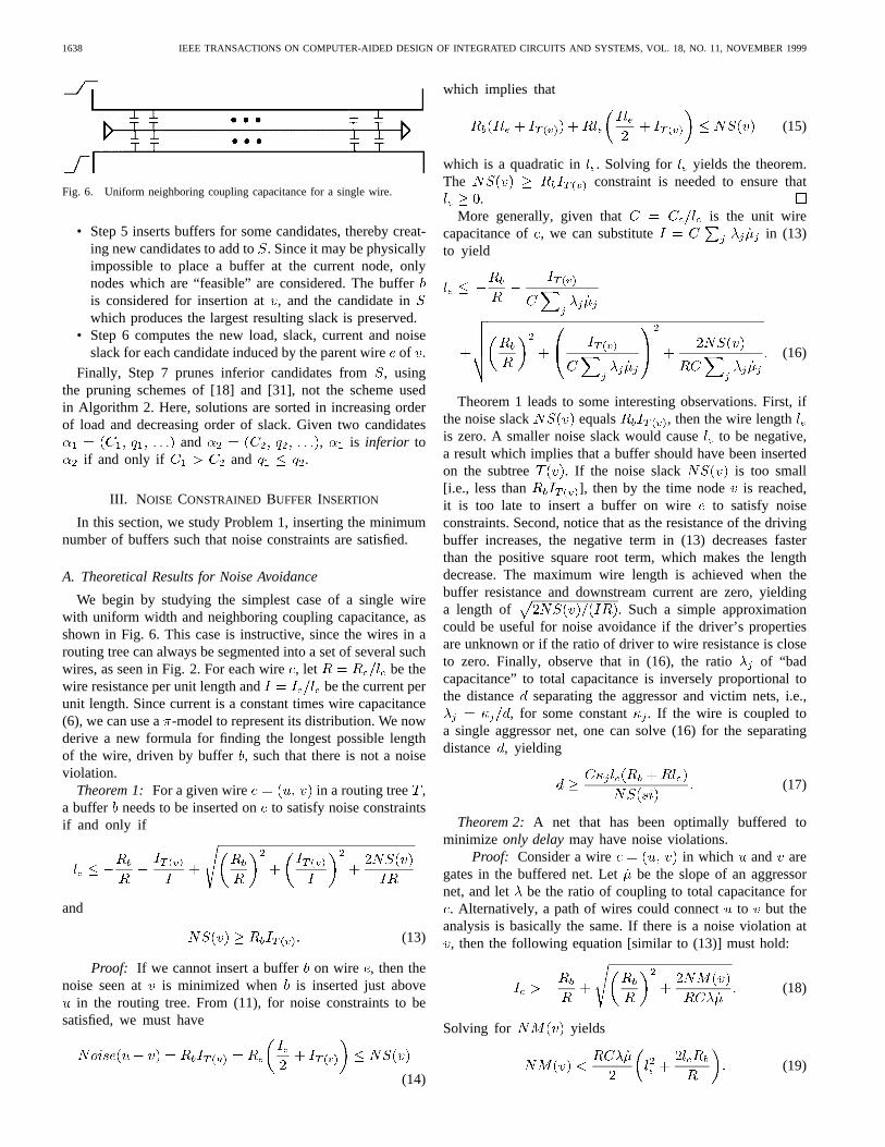
Fig. 6. Uniform neighboring coupling capacitance for a single wire.
• Step 5 inserts buffers for some candidates, thereby creat-ing new candidates to add to. Since it may be physicallyimpossible to place a buffer at the current node, onlynodes which are “feasible” are considered. The bufferis considered for insertion at, and the candidate inwhich produces the largest resulting slack is preserved.
• Step 6 computes the new load, slack, current and noiseslack for each candidate induced by the parent wireof .
Finally, Step 7 prunes inferior candidates from, usingthe pruning schemes of [18] and [31], not the scheme usedin Algorithm 2. Here, solutions are sorted in increasing orderof load and decreasing order of slack. Given two candidates
and , is inferior toif and only if and .
III. N OISE CONSTRAINED BUFFER INSERTION
In this section, we study Problem 1, inserting the minimumnumber of buffers such that noise constraints are satisfied.
A. Theoretical Results for Noise Avoidance
We begin by studying the simplest case of a single wirewith uniform width and neighboring coupling capacitance, asshown in Fig. 6. This case is instructive, since the wires in arouting tree can always be segmented into a set of several suchwires, as seen in Fig. 2. For each wire, let be thewire resistance per unit length and be the current perunit length. Since current is a constant times wire capacitance(6), we can use a-model to represent its distribution. We nowderive a new formula for finding the longest possible lengthof the wire, driven by buffer , such that there is not a noiseviolation.
Theorem 1: For a given wire in a routing tree ,a buffer needs to be inserted onto satisfy noise constraintsif and only if
and
(13)
Proof: If we cannot insert a buffer on wire , then thenoise seen at is minimized when is inserted just above
in the routing tree. From (11), for noise constraints to besatisfied, we must have
(14)
which implies that
(15)
which is a quadratic in . Solving for yields the theorem.The constraint is needed to ensure that
.More generally, given that is the unit wire
capacitance of , we can substitute in (13)to yield
(16)
Theorem 1 leads to some interesting observations. First, ifthe noise slack equals , then the wire lengthis zero. A smaller noise slack would causeto be negative,a result which implies that a buffer should have been insertedon the subtree . If the noise slack is too small[i.e., less than ], then by the time node is reached,it is too late to insert a buffer on wire to satisfy noiseconstraints. Second, notice that as the resistance of the drivingbuffer increases, the negative term in (13) decreases fasterthan the positive square root term, which makes the lengthdecrease. The maximum wire length is achieved when thebuffer resistance and downstream current are zero, yieldinga length of . Such a simple approximationcould be useful for noise avoidance if the driver’s propertiesare unknown or if the ratio of driver to wire resistance is closeto zero. Finally, observe that in (16), the ratio of “badcapacitance” to total capacitance is inversely proportional tothe distance separating the aggressor and victim nets, i.e.,
, for some constant . If the wire is coupled toa single aggressor net, one can solve (16) for the separatingdistance , yielding
(17)
Theorem 2: A net that has been optimally buffered tominimize only delaymay have noise violations.
Proof: Consider a wire in which and aregates in the buffered net. Let be the slope of an aggressornet, and let be the ratio of coupling to total capacitance for. Alternatively, a path of wires could connectto but the
analysis is basically the same. If there is a noise violation at, then the following equation [similar to (13)] must hold:
(18)
Solving for yields
(19)

ALPERT et al.: BUFFER INSERTION FOR NOISE AND DELAY OPTIMIZATION 1639
Fig. 7. Iterative application of Theorem 1.
Fig. 8. Algorithm 1: noise avoidance for single-sink tree.
For any fixed values for the parameters on the right side ofthe inequality, a noise violation will occur if the noise marginat is small enough. Even if is reasonably large,an aggressor net can have a very large slopeand a highcoupling ratio which would also cause a violation.
B. Algorithm 1: Optimal Noise Avoidance for Single-Sink Trees
Theorem 1 suggests a noise avoidance buffer insertionalgorithm for trees with only one sink. Begin at the sink nodeand work up the tree, updating the total downstream currentand noise slacks of visited internal nodes. At a given node,use Theorem 1 to find out if adding a buffer is necessary andto compute its furthest possible location up the parent wire.The algorithm terminates when the source node is reached.Fig. 7 illustrates the order in which buffers will be insertedby the algorithm.
Fig. 8 presents the description for Algorithm 1, NoiseAvoidance for Single-Sink Trees. The algorithm accepts arouting tree, and a single buffer type. Step 1 initializesthe current and noise slack of the sink node, then Steps 2–4climb up the tree visiting each node in turn. Step 3 examineswhether or not a buffer needs to be inserted on the currentwire , by computing the noise from placing a bufferat node . If this noise is less than the noise slack, then nobuffer needs to be inserted, so the algorithm computes thedownstream current and noise slack for node, then moves tothe next wire. If the noise computed in Step 3 is larger then the
noise slack, then a buffer must be inserted. Step 4 computesthe maximum length that this buffer may be inserted from,and inserts it there at a new internal node. Finally, Step 5computes the noise slack and the source and inserts a bufferright after the source if there is a noise violation (which canonly occur if ).
Theorem 3: Algorithm 1 computes an optimal solution toProblem 1 for a single-sink tree in time.
The proof of optimality follows from the fact that buffers arealways inserted their maximal distance up the tree, accordingto Theorem 1. Observe that extending Algorithm 1 to accom-modate a buffer library with multiple buffer types is trivial,since according to Theorem 1, the buffer with smallest resis-tance always yields the maximum spacing between buffers.Hence, one can equivalently obtain the optimal solution bycreating a new buffer library consisting only of the buffer inthe original library with smallest resistance.
C. Algorithm 2: Optimal Noise Avoidance for Multi-Sink Trees
It may appear fairly easy to extend Algorithm 1 to trees withmultiple sinks. However, some difficulty arises when process-ing an internal node with two children, under the followingscenario. Let , , and , respectively, bethe wire, current, and noise slack for the left (right) branchof . It may be that and , i.e., thenoise constraints for the left and right branches are satisfied.However, we may have ,which implies that merging the two branches would causea noise violation. Thus, a buffer must be placed on eitherthe left or right branch immediately following. One cannotimmediately deduce which branch to choose since we mayhave and , i.e., the left branch is moretolerant of noise than the right branch, but the left branchhas a larger downstream current which makes it more noisesensitive. The correct choice cannot be made without knowingthe characteristics and location of the gate driving, but sincethe algorithm is bottom-up, this location of this gate has notyet been determined.
To handle this additional complexity, we propose to generatea set of candidate solutions for each node and propagatethese candidate solutions up the tree, in the same spirit asin Van Ginneken’s algorithm [31]. This time, acandidateis defined as a three-tuple where isthe downstream current seen at, is the noise slackfor , and is the current solution for the subtree .
and are used to determine which candidatesto percolate up the tree, and stores the current solutionseen so far. When a node with two children is encountered,we let denote the new solution that resultsfrom merging solutions for the left and for the rightbranch of . We assign if either or
and otherwise. Whenever a nodewith two children is encountered and a buffer needs to beinserted on either the left or the right branch, candidates foreach of these two options are generated. The candidates arestored in nondecreasing order by downstream current so thatinferior solutions can be pruned in a linear pass of the current

1640 IEEE TRANSACTIONS ON COMPUTER-AIDED DESIGN OF INTEGRATED CIRCUITS AND SYSTEMS, VOL. 18, NO. 11, NOVEMBER 1999
Fig. 9. Algorithm 2: noise avoidance for multi-sink trees.
candidate list. Given two candidatesand for node , we say that isinferior to if and only if and .The complete description for Algorithm 2: Optimal NoiseAvoidance for Multi-Sink Trees, is presented in Fig. 9. Thealgorithm is recursive and is initially passed the sourceforthe tree.7
Algorithm 2 is similar to Algorithm 1, except for Steps4–7 which handle nodes with two children. Step 4 iteratesthrough each left branch candidate and each right branchcandidate using the Van Ginneken’s linear merging technique[31]. Step 5 tests whether merging the two candidates resultsin a noise violation,8 and if there is no violation, Step 7 mergesthe candidates for the two branches without inserting a buffer.
7Note that it is inefficient to storeM for each candidate. In the actualimplementation, pointers are stored for the left and right candidates, and thefinal solution can be revealed by traversing these pointers.
8We assumeRso > Rb for this test, otherwise one must test whetherthe current solutionM will have no noise violations if no more buffers areinserted. If this test yields no noise violations, then Step 7 should be executedinstead of Step 6.
If there is a violation, then two new solutions, one with a newbuffer on the left and one with a new buffer on the right, aregenerated and inserted into the current list of candidates. Whenthe algorithm terminates, the solution(s) inwith the fewestnumber of buffers is chosen.
Theorem 4: Algorithm 2 returns an optimal solution toProblem 1 for a multi-sink tree in time.
As in Algorithm 1, optimality follows from the fact thatbuffers are only inserted at their maximal distance up the tree,except for the case when the test in Step 5 holds. But inthis case, both possible buffer insertions are preserved andpropagated up the tree, and at least one of these must beoptimal. The complexity is since each node may haveas many as candidates. In practice, we believe that thealgorithm’s run time will be linear in the average case, sincethe test in Step 5 will rarely hold. As for Algorithm 1, onecan equivalently obtain an optimal solution for a buffer librarywith multiple buffer types by selecting the buffer type withsmallest resistance.
IV. OPTIMIZING DELAY WHILE
SATISFYING NOISE CONSTRAINTS
A. Algorithm 3: Noise Avoidance for Delay Minimization
To address Problem 2, simultaneous optimization of noiseand delay, we modify Van Ginneken’s optimal delay algorithm(Figs. 4 and 5) to include noise avoidance. The essence ofour modifications is the following: whenever Van Ginneken’salgorithm considers inserting a buffer into a candidate, wecheck to see if the noise constraints have been violated; ifthey have, we do not permit a buffer to be inserted. Observethat our algorithm will actually generate fewer candidatesthan Van Ginneken’s algorithm. Van Ginneken’s algorithmgenerates a set of candidates which violate noise constraintsand a set which satisfy noise constraints, while our algorithmonly generates candidates belonging to the latter set. The othermodifications are for bookkeeping purposes and to permit abuffer library with more than one buffer.
Again, a list of candidates is computed for each nodein the tree, except that this now acandidate is a five-tuple where is theload seen at , is the slack at , is the downstreamcurrent seen at , is the noise slack at , and isthe current solution. Figs. 10 and 11 illustrate Algorithm 3,which is equivalent to Van Ginneken’s algorithm except forthe modifications for noise avoidance which are shown inboldface.
Step 1 calls the Find_Noise_Candidates procedure whichreturns a list of candidate solutions that do not include thedriver’s effect on delay and noise. Step 2 adds the driver delayand computes the noise slack, then the candidate with the bestslack, such that noise constraints are satisfied, is returned inStep 3.
The Find_Noise_Candidates procedure shown in Fig. 11. Ittakes the node to be processed as input, recursively computesthe lists of possible candidates for all the nodes in ,and then returns the candidate list for node. Steps 1–4 are

ALPERT et al.: BUFFER INSERTION FOR NOISE AND DELAY OPTIMIZATION 1641
Fig. 10. Algorithm 3: noise avoidance for delay minimization.
Fig. 11. Find_Noise_Candidates procedure.
the same as in Fig. 5 except for additional bookkeeping. InStep 5, each buffer type in the library is considered forinsertion at , and the candidate in which produces thelargest resulting slacksuch that noise constraints are satisfiedis chosen. The procedure willnot insert a buffer if its causesa noise violation. This step is the fundamental modificationmade to Van Ginneken’s algorithm. Step 6 computes the newload, slack, current and noise slack for each candidate inducedby the parent wire of . Finally, Step 7 is the same as inFig. 5.
The modifications for noise avoidance do not increasethe time complexity of Van Ginneken’s algorithm; hence,Algorithm 3 has time complexity [18].
Fig. 12. Illustrations for proof of Theorem 5.
B. Optimality of Algorithm 3
Theorem 5: If and both andhold for each , then Algorithm 3 returns an
optimal solution to Problem 2.Proof: First, observe that Algorithm 3 always returns a
solution which satisfies the noise constraints (even when) since neither a buffer nor the driver is added to a candidate
if it has a noise violation. In Step 5 of the Find_Candidatesprocedure, a buffer is only added to a candidateif theaddition of the buffer does not violate the noise margins ofthe sinks that it drives. Similarly, Step 4 of Fig. 10 will onlyreturn a solution with positive noise slack.
It may seem at first that pruning candidates may cause theoptimal solution to be eliminated, since pruning is performedbased on load and timing slack, not current and noise slack.Consider candidates and
for node where and. Since is inferior to , then will be pruned
by Step 7, but perhaps will have a noise violation furtherup the tree while will not. Since subsequently becomesan illegal solution, may actually be the optimal solutionto Problem 2, but the existence of causes it to be pruned.We now show that the optimal solution will never be pruned.There are three cases, illustrated in Fig. 12.
Case 1: and both see a single gate downstream from. If this gate is a buffer for both candidates, then the wire
capacitance component of will be greater than the wirecapacitance component for since the gate loads are thesame and . Hence, the total downstream wire lengthfrom will be longer for than for . Since currentis monotone increasing in wire length, we have .And since the noise margins for the buffers are the same,
. So, if fails to meet noise constraints furtherup the tree, will fail as well, i.e., pruning does noteliminate an optimal solution.
Alternatively, if sees one of the original sinks down-stream from , while sees a buffer, then its downstreamwire length must be longer than that of, so . Clearly,it is impossible for to see a buffer downstream and for
to see a sink because then (because the buffer

1642 IEEE TRANSACTIONS ON COMPUTER-AIDED DESIGN OF INTEGRATED CIRCUITS AND SYSTEMS, VOL. 18, NO. 11, NOVEMBER 1999
has smaller input capacitance than each sink). By assumption,the sink’s noise margin is no greater than the buffer’s noisemargin, so . As before, if fails to meet noiseconstraints further up the tree then will fail as well.
Case 2: One candidate drives a single gate, and one drivesmultiple gates. Since , then must drive the singlegate since the buffer must have smaller capacitance than eitherbranch. Hence, this gate must be further up the tree then eitherof the two gates driven by . Analysis similar to that of Case1 can be applied to conclude that and ,which makes worse than in terms of both timing andnoise, so pruning will not eliminate an optimal solution.
Case 3: Each candidate sees multiple sinks downstreamfrom . In this case, it is possible to have , sincethe gate(s) driven on the left branch for may be further upthe tree than for . This means that unlike in the previoustwo cases, may violate noise constraints further up thetree, while would not. Thus, a legal solution may in effectbecome pruned by an illegal one, making it seem possible thata potentially optimal solution may be pruned. We now showthat Step 4 in Find_Candidates constructs a third solutionwhich will not be pruned, and that is inferior to bothin terms of noise and timing. This implies that could nothave been part of the optimal solution.
Decompose the loads and of and into their leftand right components: and . If
, then we can use the same analyzes from Cases 1 and2 to conclude that is inferior to in terms of both timingand noise. Thus, pruning it does not eliminate an optimalsolution. If , then either or sincedownstream current is a monotone nondecreasing functionof capacitance. If , then consists of the leftbranch of and the right branch of , otherwise, it consistsof the right branch of and the left branch of . Thus,
, and since the buffers seen atare furtherup the tree for than for and , we conclude that
, and by usingthe same arguments as in Cases 1 and 2. Finally, to showthat it is safe to prune because of the existence of ,we must show that . Decompose the slacks and
into their left and right components:and . Since is inferior to ,and hence . If consists of theleft branch of and the right branch of , then
. If consists of the right branch of andthe left branch of , then . In either case,
, which means that is inferior to in terms ofboth noise and timing.
C. Discussion
For Theorem 5, the assumptions andare somewhat realistic since one generally would
want to choose buffers with small input capacitance and highnoise margin. We observe that if is sufficiently large, thenany solution with buffer inserted would instantly be prunedsince both its capacitance and slack would be worse that thosefor the zero-buffer solution. In this case, Algorithm 3 would
fail to insert any buffers, even if the zero-buffer solution hadnoise violations.
In practice, buffers are commonly used to reduce delay oftenby decoupling off-path load capacitance. Thus, a buffer libraryshould have at least one buffer with small input capacitancerelative to the wire and sink capacitances. As long as sucha buffer exists in the library and there is sufficient wiresegmenting, Algorithm 3 will find a legal solution.
When there is more than one buffer in the buffer library,even if they all have small input capacitance, the optimalityof Algorithm 3 is not guaranteed. The proof of Theorem 5utilizes the fact that if one candidate sees more downstreamcapacitance than another candidate, then it must also see morewire capacitance, and hence, more downstream current. Sincedifferent buffer types have different input capacitances, thisassertion cannot be made. We believe that even with multiplebuffer types, Algorithm 3 will generally produce solutions thatare very close to optimal; our experimental results in Section Vstrongly support this claim.
In optimally solving Problem 2, more buffers may be addedthan necessary, e.g., six additional buffers might be insertedto squeeze out an extra 25 ps of performance. Alternatively,one may wish to minimize the number of inserted buffers suchthat noise and timing constraints are satisfied.
Problem 3: Given a tree , a bufferlibrary , and noise margins for each , finda solution which minimizes such that
and for each. Since many possible solutions may exist, maximize
as a secondary objective.We can address this formulation by incorporating an exten-
sion to Van Ginneken’s algorithm proposed by Lilliset al. [18]into Algorithm 3. Lillis et al. showed that instead of storing asingle candidate list for each node, one can store several listsin an array indexed by the total number of buffers insertedin the candidate solution. This allows one to generate theoptimal solution in terms of delay for any desired number ofbuffers. We have incorporated this extension into Algorithm 3and address Problem 3 by first finding the best solution interms of timing for each possible number of buffers and thenreturning the solution with the fewest buffers such that bothnoise and timing constraints are satisfied. This algorithm hasbeen incorporated into a tool called BuffOpt.
We have theoretically shown that optimizing delay alonecannot possibly fix all noise problems. The experimentalresults in the next section shows that this phenomenon occursin practice as well.
V. EXPERIMENTAL RESULTS
The techniques presented in the previous sections have beenimplemented in a tool called Buffopt. We refer to the algorithmwhich find the optimizes only delay [1], [18] as DelayOpt.DelayOpt is the same as Algorithm 3 in Fig. 10, withoutthe boldface modifications. However, like BuffOpt, DelayOptwas extended to be able to trade off between the degree oftiming optimization and the number of buffers inserted. Thisextension allows us to report the best result for any given

ALPERT et al.: BUFFER INSERTION FOR NOISE AND DELAY OPTIMIZATION 1643
TABLE ISINK DISTRIBUTION OF THE 500 TEST NETS
TABLE IINUMBER OF NOISE VIOLATIONS REPORTED BY
3dNOISE BEFORE AND AFTER RUNNING BuffOpt
number of buffers k, and we denote this result as DelayOpt(k).For our experiments, we selected a set of 500 nets from amodern Power PC microprocessor design. Each gate in thedesign belongs to precharacterized cell library, and timing andcapacitance data for each gate was obtained by simulation andextraction. The 500 nets with largest total capacitances werechosen for analysis, since these nets were most likely to havenoise violations. Table I shows the distribution of the sizes ofthese nets.
To verify BuffOpt, we separately ran a more detailed,simulation-based noise analysis tool, 3dnoise [26]. 3dnoisewas run both before and after running BuffOpt and DelayOpt.To perform noise analysis, 3dnoise uses accurate moment-matching based techniques that are similar to RICE [27].
We ran BuffOpt, DelayOpt and 3dnoise all in estimationmode (see Section II-B), assuming a 0.7 coupling to totalcapacitance ratio from a single aggressor net with rise time0.25 ns and a power supply voltage of 1.8 V (so 7.2). Thetolerable noise margin for every gate in the design is 0.8 V.Our buffer library contained 5 inverting and 6 noninvertingbuffers of varying power levels. Our experiments show thefollowing.
• BuffOpt eliminated every noise problem in the designdata.
• DelayOpt was unable to solve identified noise problems.• The average delay penalty from using BuffOpt instead of
DelayOpt was less than 2%.
A. BuffOpt Successfully Avoids Noise
We ran BuffOpt on the 500 nets, and observed that BuffOptidentified noise violations for 423 of the nets and success-fully inserted buffers to fix all of them. To verify BuffOpt’sidentification of noise critical nets, we ran 3dnoise on the testdata before running BuffOpt. The accurate analysis of 3dnoiseidentified 386 nets with noise violations, all of which werealso identified by BuffOpt. BuffOpt identified 423 386 37more nets with violations, which shows that the noise metricis more conservative. This is due to the fact that the noisemetric is an upper bound. To verify the ability of BuffOpt toeliminate noise violations, we ran 3dnoise on the test data afterrunning BuffOpt. 3dnoise identified no noise violations on thedata after buffers had been inserted. This data is summarizedin Table II.
TABLE IIINOISE AVOIDANCE COMPARISONS OFBuffOpt VERSUS DelayOpt(k)
TABLE IVAVERAGE DELAY REDUCTION IN PICOSECONDS FROMBUFFER INSERTION
B. Delay Alone is an Insufficient Optimization
Our next set of experiments compared BuffOpt to DelayOpt(optimal delay-driven buffer insertion) in terms of how well thealgorithms avoided noise. Since BuffOpt never inserted morethan four buffers on any net, we ran DelayOpt four times inwhich no solution was allowed to have more thanbuffers,and ranged from 1 to 4. Table III compares the solutionsgenerated by DelayOpt(k) with BuffOpt.
Observe that running DelayOpt(4) causes the addition of1126 more buffers than BuffOpt, and yet still has 13 noiseviolations. Limiting the total number of buffers inserted byDelayOpt only increases the number of noise violations andstill causes more buffers to be inserted for . Thus, as weproved in Theorem 2, noise avoidancemustbe integrated intothe problem formulation in order to avoid all noise. Finally,observe that the total CPU time for BuffOpt is actually lessthan DelayOpt(k) for . This occurs because BuffOptprunes candidate solutions which violate noise constraints,which gives BuffOpt fewer total candidates to analyze thanDelayOpt.
The total number of buffers inserted is given by netswith buffers. For example BuffOpt inserted (077)(1 161) (2 232) (3 84) (4 2) 717 buffers.
C. The Delay Penalty Is Small
Our final experiment compares DelayOpt to BuffOpt interms of total delay. We first ran BuffOpt to see how manybuffers were inserted, then ran DelayOpt for the same numberof buffers in order to make an apples to apples comparison.We computed the reduction in total delay for each net, andaveraged the results by the number of buffers inserted. Thecumulative results are presented in Table IV. For example,there were 232 nets for which two buffers were inserted, andon average BuffOpt reduced delay by 336.0 ps while DelayOptreduced delay by 338.2 ps. To find the average delay reduction

1644 IEEE TRANSACTIONS ON COMPUTER-AIDED DESIGN OF INTEGRATED CIRCUITS AND SYSTEMS, VOL. 18, NO. 11, NOVEMBER 1999
over all 423 instances, we compute the total reduction in delayfor all nets and divide by 423. For example, for BuffOpt,the weighted average is ((161124.8) (336.0 232)(1043.4 28) (45.5 2))/423 301.1.
From the last column in the table, we see that overall therewas an average delay penalty of only 6 ps, or equivalently1.99%, from avoiding noise. Thus, Buffopt is able to integratenoise into a delay-driven algorithm with virtually no loss intotal delay.
Recall that in Section IV, we proved the optimality ofAlgorithm 3 for Problem 2 under the assumption that thebuffer library contained only a single buffer type, but thatwe could not guarantee optimality for a larger buffer library.The DelayOpt results in Table IV form an upper bound on theoptimal solution to Problem 2 since it is an optimal algorithmfor minimum delay without noise constraints. Thus, we seethat even with a buffer library of size 11, BuffOpt returnsvirtually the optimal delay since it is on average within 2%of an upper bound.
VI. CONCLUSIONS
Noise is becoming an increasingly critical bottleneck inthe design process. In this work, we presented comprehensivebuffer insertion techniques for noise and delay optimization.Three algorithms were presented, the first for optimal noiseavoidance for single-sink trees, the second for optimal noiseavoidance for multi-sink trees, and the third for simultaneousnoise and delay optimization. We successfully verified ourapproach on a modern PowerPC design. We also showedboth theoretically and empirically that optimizing delay alonecannot solve all noise problems, and that the performancepenalty of optimizing both noise and delay compared to delayalone was only 2% on average.
ACKNOWLEDGMENT
The authors would like to thank J. Rahmeh for his help with3dnoise and the PowerPC design data.
REFERENCES
[1] C. J. Alpert and A. Devgan, “Wire segmenting for improved bufferinsertion,” in Proc. 34th IEEE/ACM Design Automation Conf.,1997,pp. 588–593.
[2] H. B. Bakoglu, Circuits, Interconnections, and Packaging for VLSI.Reading, MA: Addison-Wesley, 1990.
[3] C. L. Berman, J. L. Carter, and K. F. Day, “The fanout problem: Fromtheory to practice,” inAdvanced Research in VLSI: Proc. 1989 DecennialCaltech Conference,C. L. Seitz, Ed. Cambridge, MA; MIT Press, Mar.1989, pp. 69–99.
[4] I. Catt, “Crosstalk (noise) in digital systems,”IEEE Trans. Electron.Comput.,vol. ED-16, pp. 743–763, 1967.
[5] C. C. N. Chu and D. F. Wong, “Closed form solution to simultaneousbuffer insertion/sizing and wire sizing,” inProc. Int. Symp. PhysicalDesign,1997, pp. 192–197.
[6] , “A new approach to simultaneous buffer insertion and wiresizing,” in Proc. IEEE/ACM Int. Conf. Computer-Aided Design,1997,pp. 614–621.
[7] J. Cong, L. He, C.-K. Koh, and P. H. Madden, “Performance optimiza-tion of VLSI interconnect layout,”Integration: The VLSI J.,vol. 21, pp.1–94, 1996.
[8] A. Devgan, “Efficient coupled noise estimation for on-chip intercon-nects,” in Proc. IEEE/ACM Int. Conf. Computer-Aided Design,1997,pp. 147–151.
[9] S. Dhar and M. A. Franklin, “Optimum buffer circuits for driving longuniform lines,” IEEE J. Solid-State Circuits,vol. 26, pp. 32–40, Jan1991.
[10] W. C. Elmore, “The transient response of damped linear network withparticular regard to wideband amplifiers,”J. Appl. Phys.,vol. 19, pp.55–63, 1948.
[11] P. Feldmann and R. W. Fruend, “Reduced-order modeling of large linearsubcircuits via a block Lanczos algorithm,” inProc. ACM/IEEE DesignAutomation Conf.,1995, pp. 474–479.
[12] L. Gal, “On-chip crosstalk—The new signal integrity challenge,” inProc. Custom Integrated Circuits Conf.,1995, pp. 12.1.1–12.1.4.
[13] M. Z.-W. Kang, W. W.-M. Dai, T. Dillinger, and D. P. LaPotin, “Delaybounded buffered tree construction for timing driven floorplanning,” inProc. IEEE/ACM Int. Conf. Computer-Aided Design,1997, pp. 707–712.
[14] L. N. Kannan, P. R. Suaris, and H.-G. Fang, “A methodology and algo-rithms for post-placement delay optimization,” inProc. 31st IEEE/ACMDesign Automation Conf.,1994, pp. 327–332.
[15] R. Kay and L. Pileggi, “PRIMO: Probability interpretation of momentsfor delay calculation,” inProc. ACM/IEEE Design Automation Conf.,1998, pp. 463–468.
[16] D. Kirkpatrick and A. Sangiovanni-Vincentelli, “Techniques forcrosstalk avoidance in design of high-performance digital systems,”in Proc. IEEE Int. Conf. Computer-Aided Design,1994, pp. 616–619.
[17] J. Lillis, “Timing optimization for multi-source nets: Characterizationand optimal repeater insertion,” inProc. 34th IEEE/ACM Design Au-tomation Conf.,1997, pp. 214–219.
[18] J. Lillis, C.-K. Cheng, and T.-T. Y. Lin, “Optimal wire sizing andbuffer insertion for low power and a generalized delay model,”IEEE J.Solid-State Circuits,vol. 31, pp. 437–447, Mar. 1996.
[19] , “Simultaneous routing and buffer insertion for high-performanceinterconnect,” inProc. 6th Great Lakes Symp. Physical Design,1996,pp. 7–12.
[20] S. Lin and M. Marek-Sadowska, “A fast and efficient algorithm fordetermining fanout trees in large networks,” inProc. European Conf.Design Automation,1991, pp. 539–544.
[21] T. Lin, E. Acar, and L. Pileggi, “h-gamma: An RC delay metric basedon a gamma distribution approximation of the homogeneous response,”in Proc. IEEE/ACM Int. Conf. Computer-Aided Design,1998, pp. 19–25.
[22] L. W. Nagel, “SPICE2, a computer program to simulate semiconductorcircuits,” Univ. California, Berkeley, CA, Tech. Rep. ERL-M520, May1975.
[23] T. Okamoto and J. Cong, “Interconnect layout optimization by simul-taneous Steiner tree construction and buffer insertion,” inProc. 5thACM/SIGDA Physical Design Workshop,1996, pp. 1–6.
[24] P. Penfield and J. Rubinstein, “Signal delay in RC tree networks,” inProc. ACM/IEEE Design Automation Conf.,1981, pp. 613–617.
[25] L. T. Pillage and R. A. Rohrer, “Asymptotic waveform evaluationfor timing analysis,”IEEE Trans. Computer-Aided Design,vol. 9, pp.352–366, Apr. 1990.
[26] J. Rahmeh, “The 3d-noise user guide,” IBM, Austin, TX, Internal Rep.,1997.
[27] C. Ratzlaff and L. T. Pillage, “RICE: Rapid interconnect circuit eval-uator using asymptotic waveform evaluation,”IEEE Trans. Computer-Aided Design,vol. 13, pp. 763–776, June 1994.
[28] K. Shephard and V. Narayan, “Noise in submicron digital design,” inProc. IEEE/ACM Int. Conf. Computer-Aided Design,1996, pp. 524–531.
[29] T. Stohr, M. Alt, A. Hetzel, and J. Koehl, “Analysis, reduction andavoidance of crosstalk on VLSI chips,” inProc. Int. Symp. PhysicalDesign,1998, pp. 211–218.
[30] R. R Tummala and E. J. Ryamszewski,Microelectronics PackagingHandbook. New York: Van Nostrand, Reinhold, 1989.
[31] L. P. P. P. van Ginneken, “Buffer placement in distributed RC-treenetworks for minimal Elmore delay,” inProc. Int. Symp. Circuits andSystems,1990, pp. 865–868.
[32] A. Vittal and M. Marek-Sadowska, “Crosstalk reduction for VLSI,”IEEE Trans. Computer-Aided Design,vol. 16, pp. 290–298, Mar. 1997.
Charles J. Alpert (S’92–M’96) received the B.S.and the B.A. degrees from Stanford University,Stanford, CA, in 1991. He received the Ph.D. degreein computer science at the University of Californiaat Los Angeles in 1996.
He currently works as a Research Staff Member atthe IBM Austin Research Laboratory in Austin, TX.
Dr. Alpert received a Best Paper Award at boththe 1994 and 1995 ACM/IEEE Design AutomationConferences. He also serves on the program com-mittee for the International Symposium on Physical
Design. His research interests include clock distribution, noise analysis, globalrouting, and timing optimization.

ALPERT et al.: BUFFER INSERTION FOR NOISE AND DELAY OPTIMIZATION 1645
Anirudh Devgan (S’91–M’91) received the B.T.degree in electrical engineering from the IndianInstitute of Technology, Delhi, India, in 1990 andthe M.S. and Ph.D. degrees in electrical and com-puter engineering from Carnegie Mellon University,Pittsburgh, PA, in 1991 and 1993, respectively.
He is currently the Manager of electrical analysisand physical design in the IBM Server Group inAustin, TX. From 1994 to 1999, he was a ResearchStaff Member in the IBM Research Division, atIBM Thomas J. Watson Research Center, Yorktown
Heights, NY, and at IBM Austin Research Laboratory, Austin, TX. Hisresearch interests are in the area of design automation of integrated cir-cuits, specifically transistor and interconnect level modeling, analysis, andoptimization.
Stephen T. Quayreceived the B.S. degree in elec-trical engineering and the B.S. degree in computerscience from Washington University, St. Louis, MO,in 1983.
Since 1983, he has worked in many areas of chiplayout and analysis for IBM in Endicott, NY, andAustin, TX. Currently, he is an Advisory Engineerin the Server Development Group where he devel-ops design automation applications for interconnectextraction and performance optimization.


![Understanding Wireless Attacks Detection 1633[1]](https://img.pdfslide.us/doc/110x75/577cd1681a28ab9e78945ff0/understanding-wireless-attacks-detection-16331.jpg)