Embed Size (px)
Citation preview
BSMS Service ManualDAEDALUS - LOCK
Version 005
Bruker BioSpin
The information in this manual may be altered without notice.
Bruker BioSpin accepts no responsibility for actions taken as a result of use of this manual. Bruker BioSpin accepts no liability for any mistakes contained in the manual, leading to coinciden-tal damage, whether during installation or operation of the in-strument. Unauthorised reproduction of manual contents, without written permission from the publishers, or translation into another language, either in full or in part, is forbidden.
This manual was written by
C. Gosteli, B. Jud, A. Kuster, A. Schwilch, C. Schumacher
Translated and Desktop Published by
C.M. Brumby and B.Jud
Bruker BioSpin AG, CH-8117 Fällanden
© September 5, 2003: Bruker BioSpin AGFällanden, Switzerland
P/N: Z31130DWG-Nr.: 806 005
2(127) Bruker BioSpin Daedalus Lock Manual Index 005
Contents
Contents ............................................................... 3
Index ..................................................................... 7
1 Introduction ........................................................ 15
2 General Description ............................................ 172.1 Introduction ....................................................................... 172.2 Features ............................................................................ 172.3 Design ............................................................................... 192.4 Installation ......................................................................... 21
3 Operation ............................................................ 233.1 Lock Parameters ............................................................... 233.2 Manual Lock-In .................................................................. 253.3 Optimal Operation with the Digital Lock ............................. 26
Quick guide for choosing the lock parameters ................293.4 Drift Calibration Procedure ................................................ 303.5 Lock Keyboard Menu Tree ................................................. 313.6 Lock-Hold Operation .......................................................... 32
Lock-Hold Trouble shooting ...........................................33
4 19F Lock Option ................................................. 354.1 Introduction ....................................................................... 354.2 19F-Option Installation ...................................................... 354.3 19F-Wiring ........................................................................ 394.4 19F-Operation ................................................................... 40
5 Lock Transmitter ................................................. 435.1 Function Description .......................................................... 44
General .........................................................................44Digitalization of the 10 MHz Reference ...........................4560 MHz Multiplier for DDS Clock Frequency ...................45N x 10 MHz Multiplier .....................................................46Direct Digital Synthesizer (DDS) ....................................46Quadrature Mixer ...........................................................47Attenuator and Switching ...............................................47Digital-Analog Converter (DAC) .....................................48PFP / FFA-Mode Switching ............................................48FFA Amplifier .................................................................48Pulse-Section ................................................................49
Daedalus Lock Manual Index 005 Bruker BioSpin 3 (127)
Contents
Transmitter Blanking ...................................................... 51HPPR Gating Pulse TP-F0 ............................................. 52Description of the Most Important Controller Pulses: ...... 53Print (Hardware) Version ............................................... 59
6 19F TX Option ...................................................... 616.1 Function Description ......................................................... 61
General ......................................................................... 61Block Diagram ............................................................... 6119F_LO Synthesis ......................................................... 62Mixer ............................................................................. 6219F_TR Signal Path ...................................................... 6219F Lock Operation ....................................................... 63
7 Lock Receiver ...................................................... 657.1 Function Description ......................................................... 66
Concept ........................................................................ 66High Frequency -Section (HF Part) ................................ 67Low Frequency Section (LF Section) ............................. 67Aquisition ...................................................................... 68Print (Hardware) Version ............................................... 68
8 19F RX Option ...................................................... 698.1 Function Description ......................................................... 69
Print (Hardware) Version ............................................... 718.2 Connecting the 19F RX-Option .......................................... 71
9 Lock Controller .................................................... 739.1 Function Description ......................................................... 74
General ......................................................................... 74Microcontroller .............................................................. 74Address Decoder in the Lock System ............................ 75VME - Interface ............................................................. 76Reset and Power up Logic ............................................. 76RCP- Interface .............................................................. 76DSP- Host Interface ...................................................... 77DSP-Section (Hardware) ............................................... 77DSP-Section (Software) ................................................. 78Display Data .................................................................. 78Current Source .............................................................. 79Serial Interface in the Locksystem ................................. 79Lock- Software .............................................................. 81
9.2 Jumper Setting .................................................................. 829.3 Print (Hardware) Version ................................................... 83
10 Lock RS232 Piggy Board ..................................... 8510.1 General ............................................................................. 8510.2 Upgrade to ECL01 ............................................................ 85
4(127) Bruker BioSpin Daedalus Lock Manual Index 005
Contents
11 Hold Interface for AVANCE Spectrometers ........ 8711.1 Introduction ....................................................................... 8711.2 General Description ........................................................... 8711.3 Upgrade to new ECL04 ...................................................... 8811.4 Software Configuration ...................................................... 8811.5 Upgrade from LCB ECL02 to ECL03 .................................. 8911.6 Upgrade from LCB ECL03 to ECL04 .................................. 90
12 Technical Data .................................................... 9312.1 Lock Receiver Data ........................................................... 9312.2 Lock 19F Receiver Option Data ......................................... 9312.3 Lock Transmitter Data ....................................................... 9412.4 Lock 19F Transmitter Option Data ..................................... 9512.5 Lock Controller Data .......................................................... 96
13 Trouble Shooting ................................................ 9713.1 Self Test ............................................................................ 97
14 BSMS service tool .............................................. 9914.1 Init ..................................................................................... 9914.2 DownLoad ......................................................................... 9914.3 Delete Error ....................................................................... 9914.4 Version, Config.. .............................................................. 10014.5 Lock Substance ............................................................... 10014.6 Autolock Mode ................................................................. 10014.7 Magnet Type ................................................................... 10014.8 Trans Blanking On/Off ..................................................... 10114.9 Rec. Blanking On/Off ....................................................... 10114.10 Lock Hold Pulse Polarity .................................................. 10114.11 Display mode .................................................................. 10114.12 Read Lock Level .............................................................. 10214.13 Lock Shift ........................................................................ 10214.14 Lock Diagnostic ............................................................... 10314.15 Autolock H0 Calibration ................................................... 10414.16 Options ........................................................................... 10514.17 Save Lock Settings .......................................................... 10514.18 Load Lock Settings .......................................................... 10514.19 RS232 Display Baudrate .................................................. 10514.20 Lock in PWRStep ............................................................. 10514.21 L-TX TP_F0 Polarity ........................................................ 106
15 Lock Error Messages ......................................... 10715.1 Error Descriptions ............................................................ 107
16 Appendix ............................................................ 11516.1 Technical Data for the H0 Coil ......................................... 11516.2 Regulating Range ............................................................ 11616.3 Frequency Generation ..................................................... 11616.4 Chemical Shifts ............................................................... 119
Daedalus Lock Manual Index 005 Bruker BioSpin 5(127)
Contents
16.5 Frequency Coding Table .................................................. 12016.6 List of Abbreviations Used ............................................... 122
Figures ............................................................... 123
Tables ................................................................ 125
6(127) Bruker BioSpin Daedalus Lock Manual Index 005
General Description 22000000
Introduction 2.1
0 To compenstate or eliminate the effects of drift and disturbances to the magnet sy-sem, a special regulating system has been employed. Every variation in the mag-netic field brings about a change in the magnetic resonance signal.
To achieve the necessary high stability we employ a special measurement/regula-tion system known as the LOCK CHANNEL. This requires an independent, com-plete transmission/receiving channel for Deuterium that is used to stabilize the magnetic field with a regulating system.
Deuterium is added to samples that we wish to measure. In most cases Deuteri-um has no influence on the outcome of experiments conducted with the NMR sys-tem.
In special cases where Deuterium is the substance of interest an alternative lock channel can be used. This alternative channel (option) uses Fluorine as the lock substance.
The Daedalus Lock is applied to ARX, AMX, DRX, DMX, DPX-Spectrometers.
Features 2.2
0 • ULTRA LOW NOISE DESIGN
• SIGNIFICANT IMPROVEMENTS IN SHORT AND LONG TIME STABILITY
• LOWEST T1 NOISE IN 2D - SPECTRAS
• INDEPENDEND IN TEMPERATURE CHANGES
• HIGH SUPPRESSION OF MAGNETIC FIELD DISTURBANCES
• VARIABLE REGULATION PARAMETERS
• FAST SEARCH OF LOCK SIGNAL AND FAST LOCK IN (Bloch’ Regulator)
• ADJUSTABLE LOCK FREQUENCY (±1MHz)
• VARIABLE LOCK SHIFT (±200ppm)
• NARROW LOCK TRANSMITTER SPECTRUM (Blackman Window)
• COMPUTER CONTROL OF ALL LOCK PARAMETERS
• IMPLEMENTED START UP AND RUN TIME DIAGNOSTICS
• FEATURES FOR GRADIENT SPECTROSCOPY
• ALTERNATING PHASE RECEIVING
• DIGITAL SIGNAL PROCESSING IN RECEIVER AND CONTROLLER
Daedalus Lock Manual Index 005 Bruker BioSpin 17 (127)
General Description
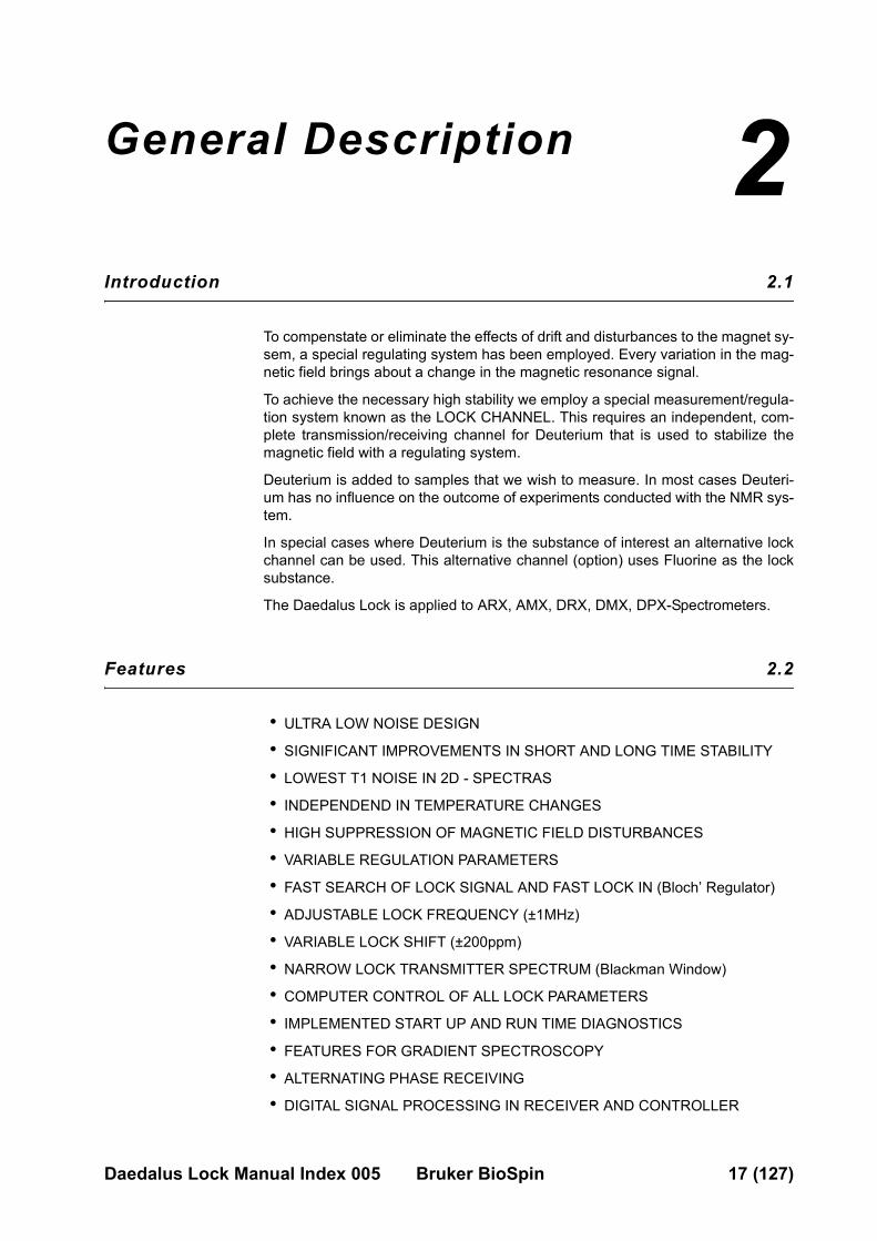
• MOUNTED in 19’ HF MOULDED CASES
• GALVANIC ISOLATION between Analog- und Digital elements
• ON FIELD change over to Fluorine (Option)
Figure 2.1. Lock Function Diagram
Mix
erB
P
H0-
Coi
l
Prob
eB
P
Mix
er
¹
Rec
tifie
r
Tran
smitt
er
ux uy
DH
reg
�m
/2
�m
/2
LO(0
°)
LO(9
0°)
Rec
tifie
r
Dig
ital S
igna
l Pro
cess
ing
Dig
ital R
egul
ator
18 (127) Bruker BioSpin Daedalus Lock Manual Index 005
Design
Design 2.3
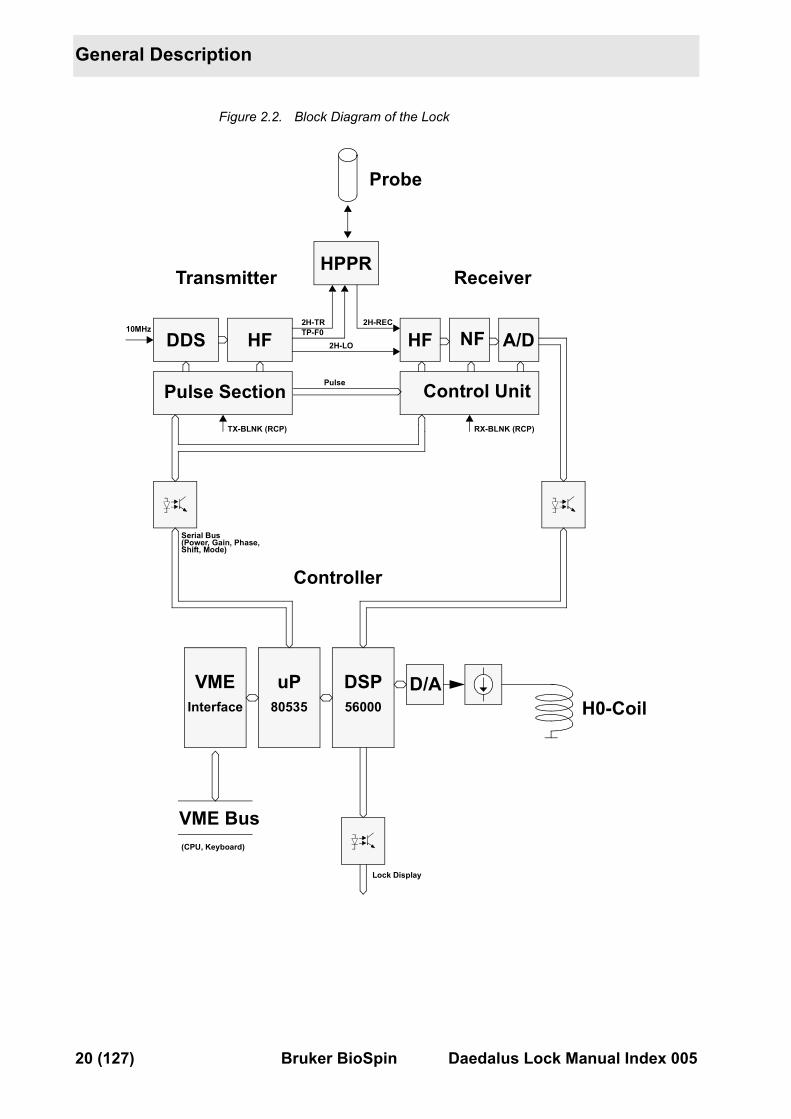
0 The Digital Lock is located on three boards. The Receiver and Transmitter are both contained in a moulded 19 inch high frequency housing. The Digital Synthe-sizer and the Pulse Section (old PFP) are located on the Transmitter. The entire frequency generation is based on a 10 MHz reference. The Power, Gain, Phase, Mode and Shift settings are conducted through a serial Bus from the Controller Board. The settings are reclocked to the Controller and checked with the originals as verification. The galvanic isolation of the Bus is located on the Transmitter.
The Bus is looped from the Transmitter to the Receiver for the Lock Gain setting. The IF-Signals (Dispersion, Absorption) are digitized in the Receiver and are seri-ally forwarded to the Controller Board via optocouplers. The sampling rate pro-ceeds at 13.3 kHz per channel. There are some other diagnostic signals which are digitized with the same A/D-Converter for diagnostic purposes.
The Controller Board receives all User or X32 commands via the VME Interface. The 80535 microprocessor is the central element of the lock system; it receives, processes and sends the commands to the various boards. All digital signal pro-cessing, including mixing, regulating and filtering, takes place in the Signal Pro-cessor. Display data for the X32 (lock line) is produced in the DSP and sent in serial form via optocouplers to the GT01 board. The H0 power source is the only analog part located on the Cotroller Board. It is also managed by the DSP.
Daedalus Lock Manual Index 005 Bruker BioSpin 19 (127)
General Description
Figure 2.2. Block Diagram of the Lock
A/DHF NF
Control Unit
DDS HF
Pulse Section
D/ADSP56000
uP80535
VMEInterface
VME Bus
HPPR
Probe
TX-BLNK (RCP) RX-BLNK (RCP)
2H-LO
2H-TRTP-F0
2H-REC10MHz
Serial Bus(Power, Gain, Phase,Shift, Mode)
H0-Coil
Lock Display
(CPU, Keyboard)
ReceiverTransmitter
Controller
Pulse
20 (127) Bruker BioSpin Daedalus Lock Manual Index 005
Installation
Installation 2.4
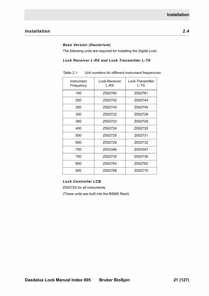
0 Base Version (Deuterium)The following units are required for installing the Digital Lock:
Lock Receiver L-RX and Lock Transmitter L-TX
Table 2.1. Unit numbers for different instrument frequencies
Lock Controller LCB Z002720 for all instruments
(These units are built into the BSMS Rack)
InstrumentFrequency
Lock-ReceiverL-RX
Lock-TransmitterL-TX
100 Z002760 Z002761
200 Z002742 Z002744
250 Z002743 Z002745
300 Z002722 Z002728
360 Z002723 Z002729
400 Z002724 Z002730
500 Z002725 Z002731
600 Z002726 Z002732
700 Z003346 Z003347
750 Z002735 Z002736
800 Z002763 Z002762
900 Z002769 Z002770
Daedalus Lock Manual Index 005 Bruker BioSpin 21 (127)

General Description
22 (127) Bruker BioSpin Daedalus Lock Manual Index 005
Operation 33000000
Lock Parameters 3.1
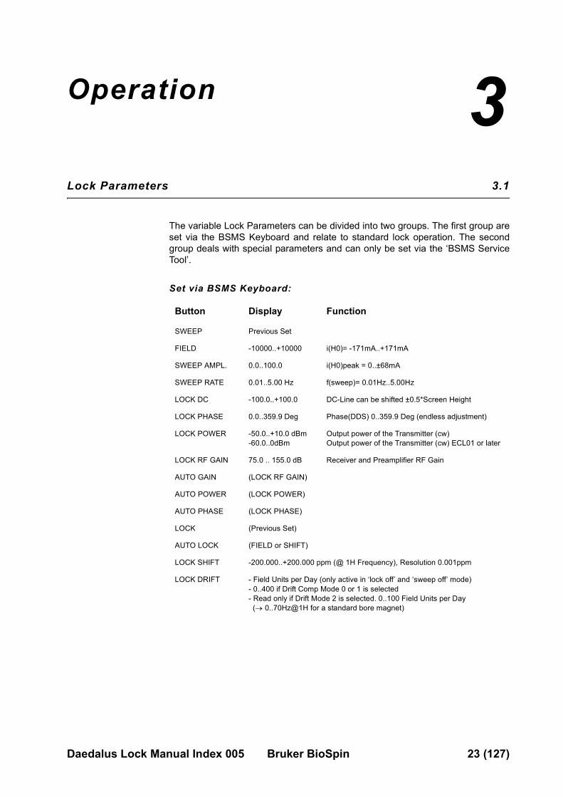
0 The variable Lock Parameters can be divided into two groups. The first group are set via the BSMS Keyboard and relate to standard lock operation. The second group deals with special parameters and can only be set via the ‘BSMS Service Tool’.
Set via BSMS Keyboard:
Button Display Function
SWEEP Previous Set
FIELD -10000..+10000 i(H0)= -171mA..+171mA
SWEEP AMPL. 0.0..100.0 i(H0)peak = 0..±68mA
SWEEP RATE 0.01..5.00 Hz f(sweep)= 0.01Hz..5.00Hz
LOCK DC -100.0..+100.0 DC-Line can be shifted ±0.5*Screen Height
LOCK PHASE 0.0..359.9 Deg Phase(DDS) 0..359.9 Deg (endless adjustment)
LOCK POWER -50.0..+10.0 dBm-60.0..0dBm
Output power of the Transmitter (cw) Output power of the Transmitter (cw) ECL01 or later
LOCK RF GAIN 75.0 .. 155.0 dB Receiver and Preamplifier RF Gain
AUTO GAIN (LOCK RF GAIN)
AUTO POWER (LOCK POWER)
AUTO PHASE (LOCK PHASE)
LOCK (Previous Set)
AUTO LOCK (FIELD or SHIFT)
LOCK SHIFT -200.000..+200.000 ppm (@ 1H Frequency), Resolution 0.001ppm
LOCK DRIFT - Field Units per Day (only active in ‘lock off’ and ‘sweep off’ mode)- 0..400 if Drift Comp Mode 0 or 1 is selected- Read only if Drift Mode 2 is selected. 0..100 Field Units per Day � (� 0..70Hz@1H for a standard bore magnet)
Daedalus Lock Manual Index 005 Bruker BioSpin 23 (127)
Operation
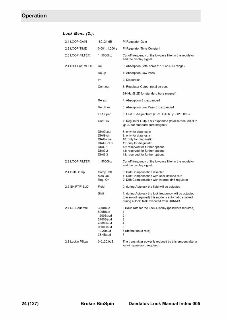
Lock Menu (2.):
2.1 LOOP GAIN -80..24 dB PI Regulator Gain
2.2 LOOP TIME 0.001..1.000 s PI Regulator Time Constant
2.3 LOOP FILTER 1..5000Hz Cut off frequency of the lowpass filter in the regulator and the display signal.
2.4 DISPLAY MODE Re 0: Absorption (total screen: 1/3 of ADC range)
Re Lp 1: Absorption Low Pass
Im 2: Dispersion
Cont.out 3: Regulator Output (total screen:
244Hz @ 2D for standard bore magnet)
Re ex. 4: Absorption 8 x expanded
Re LP ex 5: Absorption Low Pass 8 x expanded
FFA Spec 6: Last FFA-Spectrum (x: -2..+2kHz, y: -120..0dB)
Cont. ex. 7: Regulator Output 8 x expanded (total screen: 30.5Hz @ 2D for standard bore magnet)
DIAGLoLiDIAG-sinDIAG-cosDIAGCoExDIAG 1DIAG 2DIAG 3
8: only for diagnostic9: only for diagnostic10: only for diagnostic11: only for diagnostic12: reserved for further options13: reserved for further options13: reserved for further options
2.3 LOOP FILTER 1..5000Hz Cut off frequency of the lowpass filter in the regulator and the display signal.
2.4 Drift Comp Comp. OffMan OnReg. On
0: Drift Compensation disabled1: Drift Compensation with user defined rate2: Drift Compensation with internal drift regulator
2.6 SHIFT/FIELD Field 0: during Autolock the field will be adjusted
Shift 1: during Autolock the lock frequency will be adjusted (password required) this mode is automatic enabled during a ‘lock’ task executed from UXNMR.
2.7 RS-Baudrate 300Baud600Baud1200Baud2400Baud4800Baud9600Baud19.2Baud38.4Baud
0 Baud rate for the Lock-Display (password required)123456 (default baud rate)7
2.8 Lockin PStep 0.0..20.0dB The transmitter power is reduced by this amount after a lock-in (password required).
24 (127) Bruker BioSpin Daedalus Lock Manual Index 005
Manual Lock-In
Manual Lock-In 3.2
0
The first step in manually locking on a solvent when the correct field value is not known is to search for the lock signal. One approach to finding the lock signal is to set the sweep amplitude to the maximum (100), increase the lock power (e.g., to 0 dBm), and increase the lock gain (e.g., to 120 dB). The lock DC should be set to approximately –75 and the sweep rate to 0.2 Hz. Adjust the field value until the lock signal is approximately centered on the screen, and then begin to reduce the sweep amplitude. If the signal disappears from the screen during this process, it may be brought back by re-adjusting the field value. Eventually, the lock signal should be centered on the screen with the sweep amplitude reduced to a value in the range of 2 to 5. The lock power and gain should also be reduced to a level suitable to the particular solvent. Finally, the lock phase must be adjusted. The phase is optimized when the amplitude of the sweep wiggles is the same for both directions of the field sweep. If the wiggles in one direction are larger than those in the other, adjust the lock phase to correct the imbalance. Having the correct phase is important to achieving lock-in.
Caution: Sidebands
It may be difficult, especially if the lock signal is very narrow, to observe the lock signal when the sweep amplitude is fully open, despite the high power and gain settings suggested above. If this is the case, reduce the sweep amplitude. How-ever, be warned that before locking in on an unfamiliar solvent, it is important to verify that the lock signal observed is the parent signal and not a sideband. Al-though it is possible to lock on a sideband, the poorer signal-to-noise ratio of the sideband will result in a poorer overall lock performance. One way to verify that the lock signal is not a sideband, once the lock signal is centered on the screen, is to set the field value to +/–5300 units (for a standard bore magnet, more for a wide bore magnet). After changing the field value it is necessary to wait a few seconds as the actual magnetic field follows slowly (due to eddy-current effects). If the orig-inal signal was indeed the parent signal, the signal observed now is a sideband and has a much lower signal amplitude. Be sure to lock on the signal with the highest amplitude.
A second caution is that optimum lock performance will only be achieved if the lock power level is set somewhat below saturation (as described below). Thus, when using lock solvents which saturate easily (e.g., Acetone-d6), the lock power should be set rather low, ideally around –20 dBm.
Once the sweep wiggles of the parent signal are centered on the screen, have the correct phase, and are at least 1/3 the height of the screen, lock-in may be started by pressing the [LOCK ON/OFF] key. If the wiggles are too small adjust the lock gain to compensate. A strong regulator is used for the first moment of lock-in to establish the correct field value. If lock-in is successful, a second regulator then automatically takes over, the [LOCK ON/OFF] LED stops blinking, and the lock power is reduced. This second regulator uses the parameters (described below) set from the BSMS keyboard or computer.
Once lock-in is achieved, the overall lock results can be improved by adjusting the lock phase to produce the maximum signal amplitude.
Daedalus Lock Manual Index 005 Bruker BioSpin 25 (127)
Operation
Optimal Operation with the Digital Lock 3.3
0 The ‘lock’ command
One advantage of the digital lock system provided by the BSMS is that the user is no longer restricted to adjusting the field value to find the lock signal. It is now also possible to adjust the actual frequency of the lock channel. This is advantageous because it allows very nearly the same magnetic field (H0) value to be used for all lock solvents. When the same H0 value is used, the absolute frequency of the ref-erence (e.g., TMS) signal remains approximately the same, regardless of the sol-vent, and thus spectral referencing is no longer solvent dependent. In addition, if the absolute frequency of the TMS signal no longer varies from sample to sample, it now makes sense to define the offset frequencies of the observe and decouple channels in terms of ppm rather than Hz. This is helpful to the chemist who is used to thinking of chemical shifts in terms of ppm and not Hz, and who would know the offset frequencies in ppm appropriate for a particular sample.
From the BSMS keyboard itself it is possible to adjust the frequency of the lock channel by first placing the keyboard in shift mode (see Lock Parameters on page 23), pressing the [LOCK SHIFT] key, and then selecting the frequency (in ppm) with the control knob (password required). A more convenient way is to execute the „lock“ command from the UXNMR. A window occurs where the desired lock nucleus can be selected and then the Lock Transmitter is automatically being set to the corresponding frequency and an „Autolock“ command is being executed.
A second advantage of the digital lock is that it allows the user to optimize the reg-ulator used to control H0 once lock-in has been achieved. Currently, there are three lock parameters (loop gain, loop time and loop filter) available in the menu mode of the BSMS keyboard, which enable the user to control the behavior of this regulator. The following briefly describes how to set these lock parameters, in ad-dition to the standard lock parameters, for the best lock results.
During shimming, these lock parameters are not terribly important. It is important, however, to set the lock power approximately 6 to 10 dB under saturation and to optimize the lock phase.
Optimization Lock-Power and Lock-Gain
During critical NMR experiments (e.g., difference experiments), it is very important to have good shim values and optimal lock parameters to ensure good field stabil-ity. The most important indicator of an optimal lock parameter set is a high signal-to-noise ratio of the lock signal. To achieve this, first the lock power should be set as high as possible and yet not so high as to cause saturation. Increase the lock power in small steps and observe the lock line on the screen. The lock level should increase steadily in response to the increase in power level; when it no longer increases, or even begins to decrease, saturation has been reached. De-pending on the lock solvent, this may happen rather quickly (e.g., at approximate-ly –30 dBm for Acetone). The optimum lock power level is a few dB below saturation.
It is also important to choose the best lock receiver gain (lock gain). In general, if the lock DC is set appropriately (i.e., at approximately –75) it is sufficient to set the lock gain so that the lock line is in the upper part of the screen. The goal here is to best use the ranges of the A/D converter and the number range of the signal pro-cessor. This occurs when the lock gain is set as high as possible without causing receiver gain overflow, which can be recognized by the presence of a very noisy lock signal, and a decrease in lock level with a further increase in lock gain.
26 (127) Bruker BioSpin Daedalus Lock Manual Index 005
Optimal Operation with the Digital Lock
Optimization Loop-Gain, Loop-Time and Loop-Filter
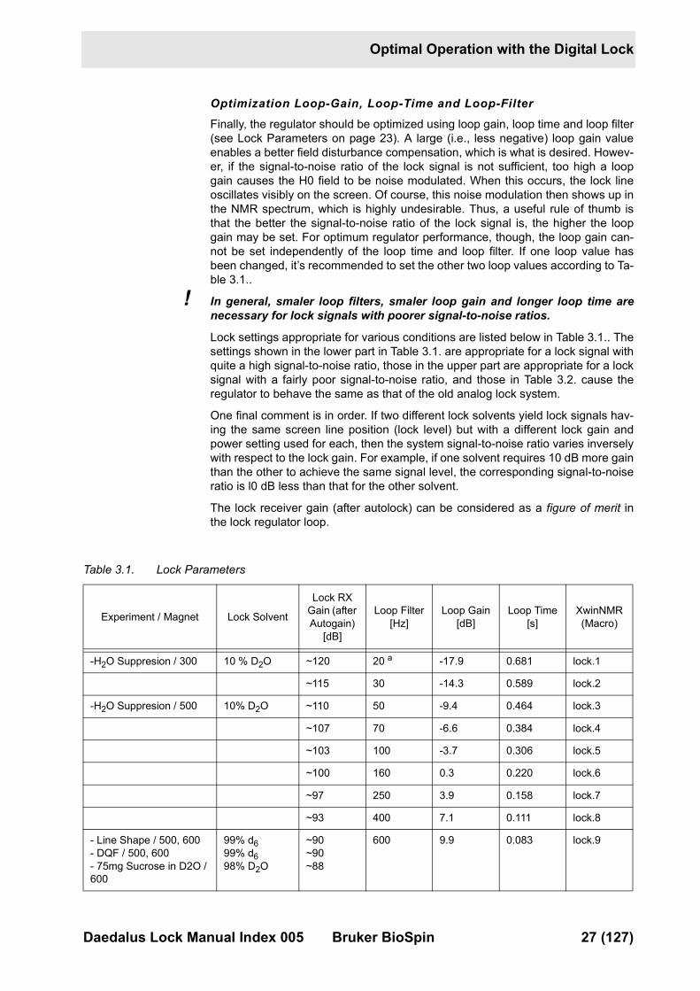
Finally, the regulator should be optimized using loop gain, loop time and loop filter (see Lock Parameters on page 23). A large (i.e., less negative) loop gain value enables a better field disturbance compensation, which is what is desired. Howev-er, if the signal-to-noise ratio of the lock signal is not sufficient, too high a loop gain causes the H0 field to be noise modulated. When this occurs, the lock line oscillates visibly on the screen. Of course, this noise modulation then shows up in the NMR spectrum, which is highly undesirable. Thus, a useful rule of thumb is that the better the signal-to-noise ratio of the lock signal is, the higher the loop gain may be set. For optimum regulator performance, though, the loop gain can-not be set independently of the loop time and loop filter. If one loop value has been changed, it’s recommended to set the other two loop values according to Ta-ble 3.1..
! In general, smaler loop filters, smaler loop gain and longer loop time are necessary for lock signals with poorer signal-to-noise ratios.
Lock settings appropriate for various conditions are listed below in Table 3.1.. The settings shown in the lower part in Table 3.1. are appropriate for a lock signal with quite a high signal-to-noise ratio, those in the upper part are appropriate for a lock signal with a fairly poor signal-to-noise ratio, and those in Table 3.2. cause the regulator to behave the same as that of the old analog lock system.
One final comment is in order. If two different lock solvents yield lock signals hav-ing the same screen line position (lock level) but with a different lock gain and power setting used for each, then the system signal-to-noise ratio varies inversely with respect to the lock gain. For example, if one solvent requires 10 dB more gain than the other to achieve the same signal level, the corresponding signal-to-noise ratio is l0 dB less than that for the other solvent.
The lock receiver gain (after autolock) can be considered as a figure of merit in the lock regulator loop.
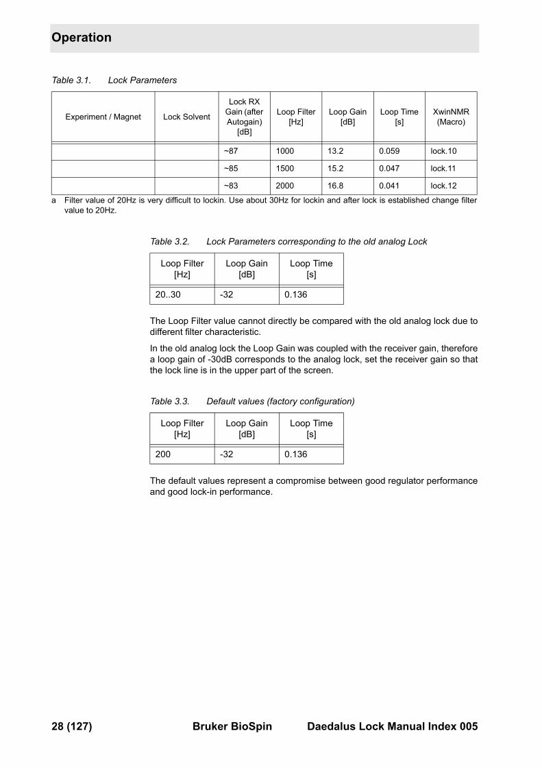
Table 3.1. Lock Parameters
Experiment / Magnet Lock Solvent
Lock RX Gain (after Autogain)
[dB]
Loop Filter[Hz]
Loop Gain[dB]
Loop Time[s]
XwinNMR(Macro)
-H2O Suppresion / 300 10 % D2O ~120 20 a -17.9 0.681 lock.1
~115 30 -14.3 0.589 lock.2
-H2O Suppresion / 500 10% D2O ~110 50 -9.4 0.464 lock.3
~107 70 -6.6 0.384 lock.4
~103 100 -3.7 0.306 lock.5
~100 160 0.3 0.220 lock.6
~97 250 3.9 0.158 lock.7
~93 400 7.1 0.111 lock.8
- Line Shape / 500, 600- DQF / 500, 600- 75mg Sucrose in D2O / 600
99% d699% d698% D2O
~90~90~88
600 9.9 0.083 lock.9
Daedalus Lock Manual Index 005 Bruker BioSpin 27 (127)
Operation
The Loop Filter value cannot directly be compared with the old analog lock due to different filter characteristic.
In the old analog lock the Loop Gain was coupled with the receiver gain, therefore a loop gain of -30dB corresponds to the analog lock, set the receiver gain so that the lock line is in the upper part of the screen.
The default values represent a compromise between good regulator performance and good lock-in performance.
~87 1000 13.2 0.059 lock.10
~85 1500 15.2 0.047 lock.11
~83 2000 16.8 0.041 lock.12
a Filter value of 20Hz is very difficult to lockin. Use about 30Hz for lockin and after lock is established change filter value to 20Hz.
Table 3.2. Lock Parameters corresponding to the old analog Lock
Loop Filter[Hz]
Loop Gain[dB]
Loop Time[s]
20..30 -32 0.136
Table 3.3. Default values (factory configuration)
Loop Filter[Hz]
Loop Gain[dB]
Loop Time[s]
200 -32 0.136
Table 3.1. Lock Parameters
Experiment / Magnet Lock Solvent
Lock RX Gain (after Autogain)
[dB]
Loop Filter[Hz]
Loop Gain[dB]
Loop Time[s]
XwinNMR(Macro)
28 (127) Bruker BioSpin Daedalus Lock Manual Index 005
Optimal Operation with the Digital Lock
Quick guide for choosing the lock parameters 3.3.1
No external field disturbances and no vibrationsUse the default values as shown in Table 3.2.
Strong external field disturbances and good lock signalCritical NMR experiments during strong field disturbances demand optimized lock parameters. Use triple values in the lower part of Table 3.1.
Strong external field disturbances and poor lock signalThis situation is one of the most difficult. A compromise between noise modulation caused by the poor lock signal and the effects of the field disturbances must be found. In this case it’s very important to work just a few dBs below the saturation of the lock signal. If the noise modulation dominates then use triple values one step higher in Table 3.1.
Strong vibrationsVibrations cannot completely be suppressed by the lock. With a very strong lock signal an acceptable suppression can be achieved. In all other cases the vibration must be mechanically damped.
Daedalus Lock Manual Index 005 Bruker BioSpin 29 (127)
Operation
Drift Calibration Procedure 3.4
0 The [DRIFT] function enables compensation of the magnetic field drift (in field units per day) during a long term measurement performed without lock. In order for [DRIFT] to provide the correct compensation, it is necessary to calibrate the magnetic field drift as follows:
1. Set the drift to zero ([2nd], [DRIFT], and choose 0 with the control knob).
2. Insert a sample with a strong lock signal.
3. Switch lock off ([LOCK ON/OFF]).
4. Switch sweep on ([SWEEP]).
5. Adjust the H0 field value until the sweep wiggles are centered on the screen ([FIELD]).
6. Press [STD BY] and wait for 24 hours without any action on spectrometer.
7. After 24 hours, enter diff-mode ([DIFF.MODE]) and select [FIELD].
8. Adjust the field value to return the sweep wiggles to the center of the screen as in step 5.. Notice the � value displayed on the right-hand side of the display.
9. Select drift ([2nd], [DRIFT]) and set this parameter to the � value found in step 8. with the same polarity. This completes the drift adjustment and further cor-rections are usually not necessary.
10. To save the drift value, first select the menu on the keyboard ([2nd] and [Y3]).
11. Enter the security code (‘4. Service’, [ENTER], ‘4.1 Sec.-Code’, [ENTER], en-ter the code with control knob and [ENTER], a beep sounds if the code is cor-rect, [ESC], and you are now in the submenu ‘4. Service’).
12. Save the drift by saving the BSMS configuration (‘4. Service’, [ENTER], ‘4.2 Save Config’, [ENTER], you hear a beep and the message ‘Done’ appears).
13. Leave the menu ([ESC], [ESC], ‘Standby’).
Once [DRIFT] has been set to a non-zero value, magnetic field drift compensation occurs when both lock and sweep are off.
30 (127) Bruker BioSpin Daedalus Lock Manual Index 005
Lock Keyboard Menu Tree
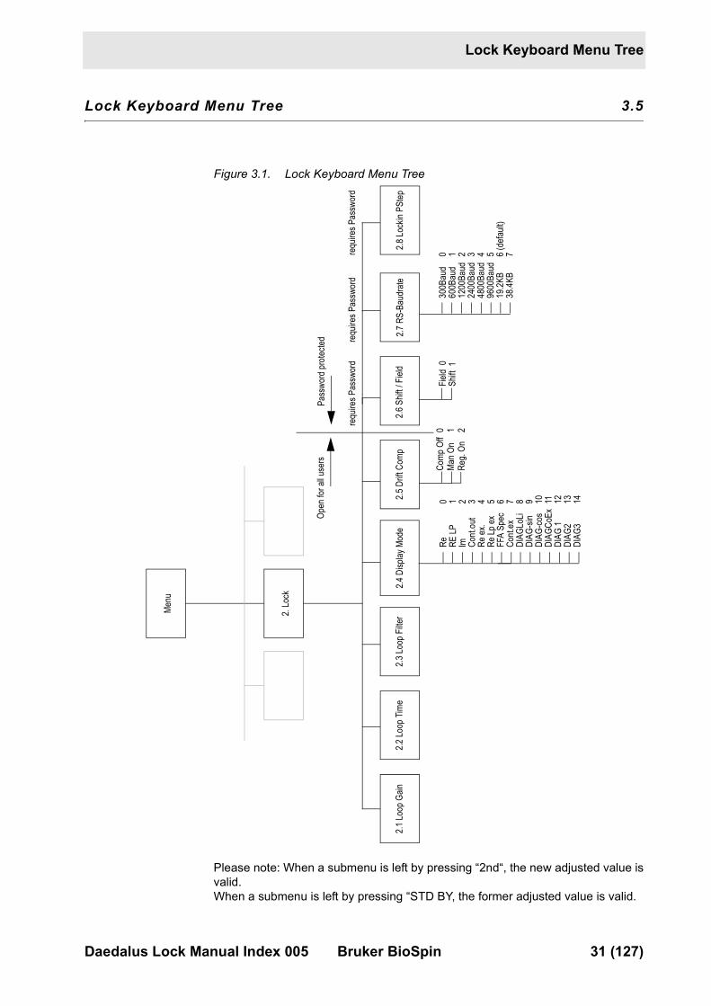
Lock Keyboard Menu Tree 3.5
0
Figure 3.1. Lock Keyboard Menu Tree
Please note: When a submenu is left by pressing “2nd“, the new adjusted value is valid.�When a submenu is left by pressing “STD BY, the former adjusted value is valid.
Menu
2. Lo
ck
2.1
Loop
Gain
2.2 Lo
op T
ime
2.4 D
isplay
Mod
e2.
6 Shif
t / F
ield
2.3 L
oop
Filte
r
requ
ires P
assw
ord
2.7 R
S-Ba
udra
te
requ
ires P
assw
ord
300B
aud
600B
aud
1200
Baud
2400
Baud
4800
Baud
9600
Baud
19.2
KB38
.4KB
Field
0Sh
ift 1
Re RE L
PIm Co
nt.o
utRe
ex.
Re L
p ex
FFA
Spec
Cont
.ex
DIAG
LoLi
DIAG
-sin
DIAG
-cos
DIAG
CoEx
DIAG
1DI
AG2
DIAG
3
2.8 L
ockin
PSt
ep
requ
ires P
assw
ord
Pass
word
prot
ected
Open
for a
ll use
rs
2.5 D
rift C
omp
Comp
Off
Man O
nRe
g. On
0 1 2 3 4 5 6 7 8 9 10 11 12 13 14
0 1 2
0 1 2 3 4 5 6 (de
fault
)7
Daedalus Lock Manual Index 005 Bruker BioSpin 31 (127)
Operation
Lock-Hold Operation 3.6
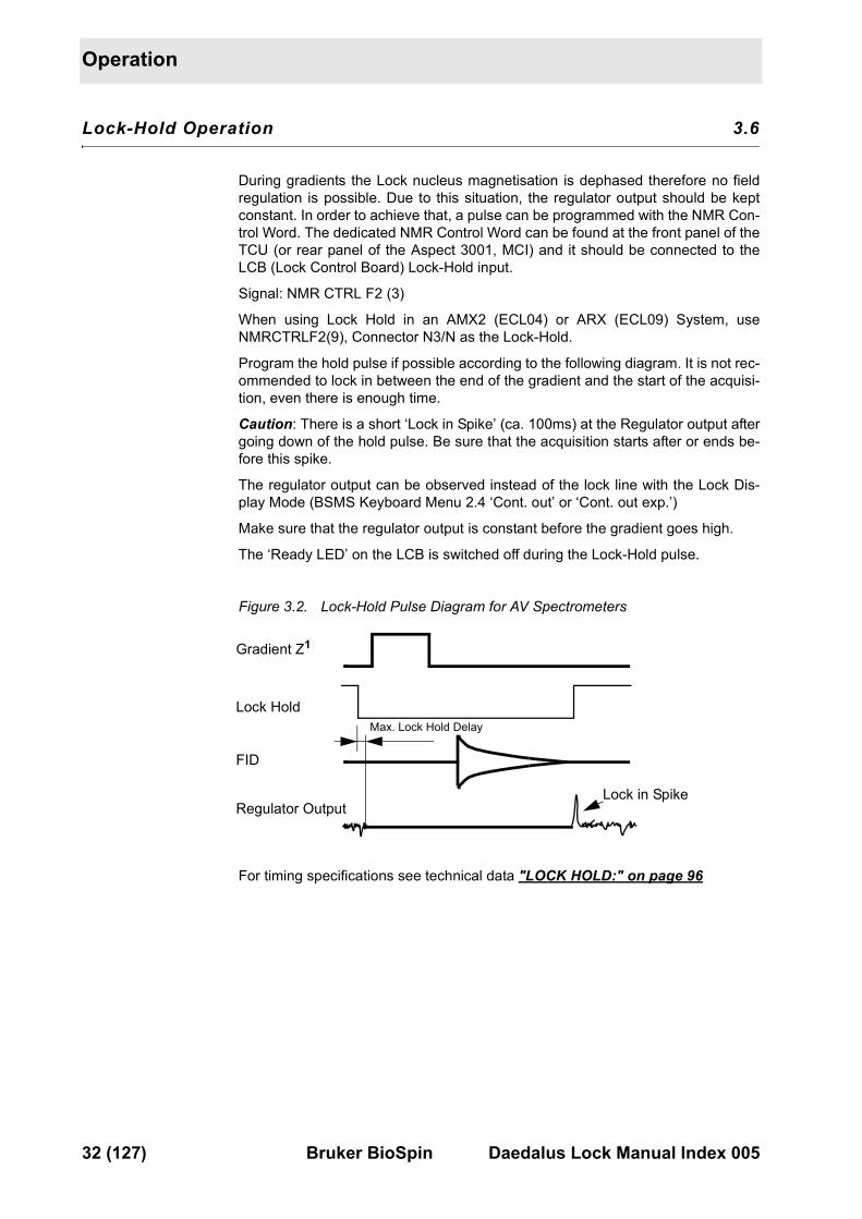
0 During gradients the Lock nucleus magnetisation is dephased therefore no field regulation is possible. Due to this situation, the regulator output should be kept constant. In order to achieve that, a pulse can be programmed with the NMR Con-trol Word. The dedicated NMR Control Word can be found at the front panel of the TCU (or rear panel of the Aspect 3001, MCI) and it should be connected to the LCB (Lock Control Board) Lock-Hold input.
Signal: NMR CTRL F2 (3)
When using Lock Hold in an AMX2 (ECL04) or ARX (ECL09) System, use NMRCTRLF2(9), Connector N3/N as the Lock-Hold.
Program the hold pulse if possible according to the following diagram. It is not rec-ommended to lock in between the end of the gradient and the start of the acquisi-tion, even there is enough time.
Caution: There is a short ‘Lock in Spike’ (ca. 100ms) at the Regulator output after going down of the hold pulse. Be sure that the acquisition starts after or ends be-fore this spike.
The regulator output can be observed instead of the lock line with the Lock Dis-play Mode (BSMS Keyboard Menu 2.4 ‘Cont. out’ or ‘Cont. out exp.’)
Make sure that the regulator output is constant before the gradient goes high.
The ‘Ready LED’ on the LCB is switched off during the Lock-Hold pulse.
Figure 3.2. Lock-Hold Pulse Diagram for AV Spectrometers
For timing specifications see technical data "LOCK HOLD:" on page 96
Gradient Z1
Lock Hold
FID
Regulator OutputLock in Spike
Max. Lock Hold Delay
32 (127) Bruker BioSpin Daedalus Lock Manual Index 005
Lock-Hold Operation
Example of a Lock-Hold Pulse Program:; xxx.setf2_3
; january 1993
; program to control NMRCONTROL F2 #3
; written based on UXNMR 921218 on ARX500
1 ze
2 d30 setf2^3 ; lock hold on
3 d31 setf2|3 ; lock hold off
6 go=2
7 exit
; e.g. d30=10ms
; e.g. d31=20ms
Lock-Hold Trouble shooting 3.6.1
• The console wiring may be different. The L_Hold RCP pulse may be connect-ed to an other NMR Control Word as described above. Check your hardware installation and use then the right sequence in the UXNMR pulse program (e.g setf2^3).
The BSMS LOCK activates the Lock Hold without a RCP pulse.• The RCP signal ground may not be connected. The interface is floating.
• With LCB boards ECL03 (or lower) in AVANCE spectrometers: The TCU may drive the RCP pulses temporary high impedance, the LCB triggers an inter-rupt.
• Upgrade the LCB to ECL04. The L_Hold interface is configurable with software to either MCI AMX, ARX or TCU DRX, DMX applications.
The LOCK regulator acts inverse to the connected L_Hold pulse. • The NMR Control Word sequence in the UXNMR pulse program may be
wrong. (e.g setf2^3 or setf2|3)�Make sure, that the pulse polarity in your UXNMR pulse program behaves as described above in "Lock-Hold Pulse Diagram for AV Spectrometers" on page 32.
• With LCB boards ECL04 (or later). The L_Hold interface is wrong configured. Configure the interface with the BSMS tool.
! Important:
The Lock Hold State must be left when the configuration is changed. The Lock software does not accept a new interface configuration while the Hold state is ac-tive. Drive the RCP pulse with the proper logic level before the interface is recon-figured.
The Hold interrupt is not free from delay. Make sure that the regulator is switched off at least 2msec before the gradients start. Program at least 2msec to recover
Daedalus Lock Manual Index 005 Bruker BioSpin 33 (127)
Operation
from a L_Hold interrupt before an other L_Hold interrupt is asserted. �For timing specifications see technical data "LOCK HOLD:" on page 96
All AVANCE spectrometers use negative logic, the RCP pulse is therefore invert-ed.
34 (127) Bruker BioSpin Daedalus Lock Manual Index 005
19F Lock Option 44000000
Introduction 4.1
0 In order to lock on to a substance other than Deuterium, option boards must be built into the Lock-Receiver and Lock-Transmitter.
The descriptions in this chapter deal with 19F as lock substance.
The entire Fluorine-Option consists of two BSMS modules (BSMS L-RX Option 19F, BSMS L-TX Option 19F), a HPPR 19F-Selective module, a special probe-head for 19F Lock purpose and some cables.
Each Deuterium-Lock can be upgraded with a Fluorine-Option in the field very easily.
The HPPR 19F-Selective module can also be used for observe applications.
19F-Option Installation 4.2
0 The following units are required for installing the Fluorine-Lock-Option:
Table 4.1. BSMS Unit numbers for different instrument frequencies
InstrumentFrequency
L-RXOption19F
L-TXOption19F
19F PREAMP MODULE HPPR HPPR/2
200
Z002748
Z002749 Z002686 Z003489
250 Z002750 Z002691 Z003490
300 Z002751 Z002599 Z003491
360 Z002752 Z002601 Z003492
400 Z002753 Z002601 Z003493
500 Z002754 Z002602 Z003494
600 Z002755 Z002603 Z003495
750 Z002756 ---- Z003497
Daedalus Lock Manual Index 005 Bruker BioSpin 35 (127)
19F Lock Option
CablesCable Set BSMS 19F-Option Z12318 (including the following two cables)
• 19F-LO Cable Z1740 (SMA/SMA)
• 19F-TR Cable Z12257 (N/SMA)
• Probehead-Cable Z2743 RG214 1.2M (BNC/N)
The two BSMS modules are realised as plug in modules. Voltage supply and con-trol signals are connected by a print single-in-line plug. HF signals are connected directly to the Receiver/Transmitter main board with SMB print connectors.
The signal from the ‘L-TX Option 19F’ board (e.g. 19F_LO and 19F_TR) are con-nected to the front panel of the Lock-Transmitter (L-TX) case via coaxial cables with SMA connectors. Before screw on the SMA connector the front foil has to be pierced through at the corresponding point with a sharp object.
The 19F_LO signal to the ‘L-RX Option 19F’ board has to be connected in the same way.
36 (127) Bruker BioSpin Daedalus Lock Manual Index 005
19F-Option Installation
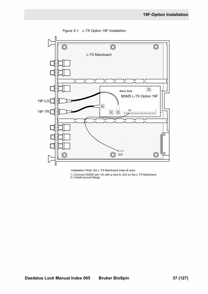
Figure 4.1. L-TX Option 19F Installation
1
Back Side
BSMS L-TX Option 19F
L-TX Mainboard
19F-TR
19F-LO
JU2
Installation Hints: (for L-TX Mainboard Index B only)1.) Connect DGND (pin 14) with a wire to JU2 on the L-TX Mainboard
.
14
2.) Install second flange
Daedalus Lock Manual Index 005 Bruker BioSpin 37 (127)
19F Lock Option
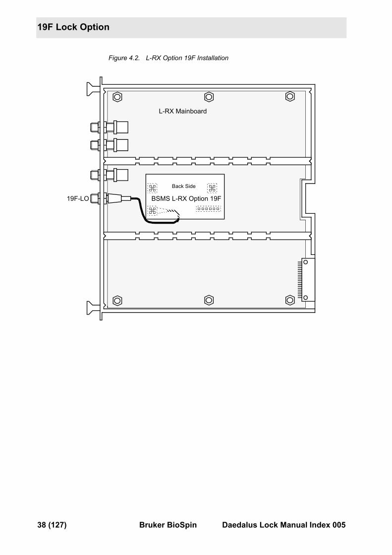
Figure 4.2. L-RX Option 19F Installation
Back Side
BSMS L-RX Option 19F
L-RX Mainboard
19F-LO
38 (127) Bruker BioSpin Daedalus Lock Manual Index 005
19F-Wiring
19F-Wiring 4.3
0
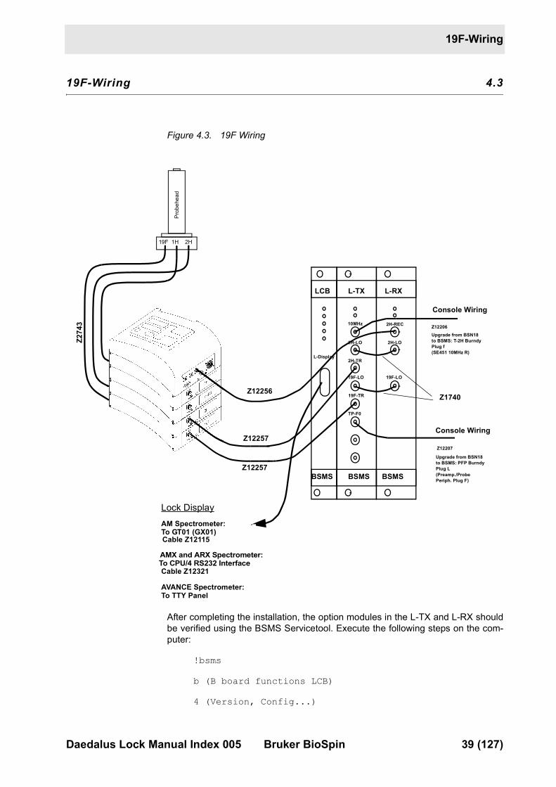
Figure 4.3. 19F Wiring
After completing the installation, the option modules in the L-TX and L-RX should be verified using the BSMS Servicetool. Execute the following steps on the com-puter:
!bsms
b (B board functions LCB)
4 (Version, Config...)
2H19F 1H
Prob
ehea
d
BSMSBSMS
L-TX L-RXLCB
BSMS
19F-LO19F-LO
19F-TR
2H-LO2H-LO
10MHz 2H-REC
2H-TR
TP-F0
Upgrade from BSN18to BSMS: PFP BurndyPlug L(Preamp./ProbePeriph. Plug F)
Upgrade from BSN18 to BSMS: T-2H BurndyPlug f(SE451 10MHz R)
Z12257
Z12257
Z274
3
Z12256Z1740
AM Spectrometer:
Cable Z12115
L-Display
Lock Display
Console Wiring
Z12206
Z12207
Console Wiring
To CPU/4 RS232 InterfaceCable Z12321
To GT01 (GX01)
AMX and ARX Spectrometer:
AVANCE Spectrometer:To TTY Panel
Daedalus Lock Manual Index 005 Bruker BioSpin 39 (127)
19F Lock Option
The BSMS will inform you the actual Lock configuration (example for 500Mhz unit):
Receiver 8 Type 500MHz
Transmitter 8 Type 500MHz
Rec Option 1 Fluorine Option
Trans Option 1 Fluorin Option 1
This means the complete 19F-Option is acknowledged by the software and 19F operation can start.
19F-Operation 4.4
0 In 19F mode most Lock-Parameters have the same effect as in 2H mode. The fol-lowing part is a description of Lock-Parameters which are different from regular 2H mode.
The 19F mode can be activated from the Acquisition-Parameters in the UXNMR (not implemented in version 920801). Select the 19F lock nucleus and after the next ‘ii’ the BSMS and the HPPR were switching to 19F.
There is an other possibility to assert the 19F mode in the BSMS. Execute the fol-lowing commands with the BSMS-Servicetool:
!bsms
B board functions LCB � B
5 Lock Substance � 5
Read or Write Lock Substance? [R,W] � w
Select Lock Substance: 0=Deuterium 1=Option �Enter Value �1
After these steps, the BSMS service tool can be exited. The 2H mode could be activated in the same manner by selecting 0 (Deuterium) as the lock substance.
The 19F signals from the probehead are much more stronger then the 2H signals. Because of this fact the receiver gain in the entire 19F receiver path is 20 dB less than the gain in the 2H receiver path.
Set the right Lock-Shift if the compound is known (see table ‘Chemical Shifts’ in section A). The Lock-Shift can be set directly in ppm on the BSMS-Keyboard. If it doesn’t appear any signal on the screen try to search for it in the same way as in the 2H mode.
Because of the higher frequency of the 19F nucleus, H0 changes are much more sensitive. Use a Sweep Rate about six times less than in the 2H mode.
The regulating characteristic in 19F mode is also different from 2H mode. After re-ducing the Loop Gain by 15dB, regulating characteristic will correspond with the 2H mode.
1 This does not working correctly with L-TX ECL00
40 (127) Bruker BioSpin Daedalus Lock Manual Index 005
19F-Operation
Lock Settings for 19F which correspond to the old Analog-LockLoop Gain: -47 dBLoop Time: 0.136 s
Daedalus Lock Manual Index 005 Bruker BioSpin 41 (127)

19F Lock Option
42 (127) Bruker BioSpin Daedalus Lock Manual Index 005
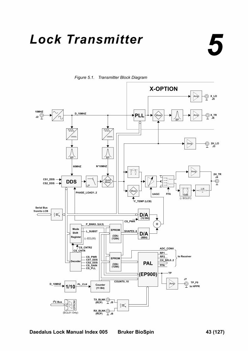
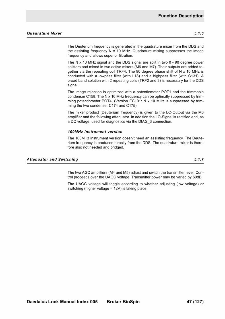
Lock Transmitter 55000000
Figure 5.1. Transmitter Block Diagram
D/A
D/A
LP
Mixer
PAL
(EP900)
EPROM
(32k)
EPROM
(32k)
1/10 Counter(11 Bit)
ModeShift
Register
Decoder
D_10MHZ
TX_BLNK
RX_BLNK
Serial Bus
(12 Bit)
(8Bit)
SHAPE0..6
COUNT0..10PL_CLK
ADC_CONVRP1RP2CH_SEL0..2
FFA
to Receiver
Amp TP_F0to HPPR
TP
DDS
PHASE_LOAD1..2
CS_CNTR
CS_PWRCS1_DDSCS2_DDSCS_GAINCS_PLL
CS1_DDSCS2_DDS
CS_PWRP_BNK0..3(4,5)
Mixer
Amp
Amp
�/4
BP BP
PLL Mixer
BP
Amp
Amp
Quad
F_TEMP (LCB)
2H_TR
2H_LO
X_TR
X_LO
10MHZ
(RCP)
(RCP)
X-OPTION
D_10MHZ
60MHZ N*10MHZ
L_SUBST
UAGC
J5
J6
J3
J4
J9
J8
J2
FFA
J7
from/to LCB
I2 C
I2C Bus
EPR
OM
10dB(� ECL01)
(ECL01 Only)
CS_CNTR2
(128k)
(128k)
(��ECL05)
Daedalus Lock Manual Index 005 Bruker BioSpin 43 (127)
Lock Transmitter
Function Description 5.1
0
General 5.1.1
The Deuterium transmitter signal (2H_TR) and the Deuterium local oscillating sig-nal (2H_LO) are generated in the HF section of the Lock Transmitter using an ex-ternal 10MHz Reference Signal. The base version is equipped with a Deuterium Lock.
The Transmitter is mounted on one four layer board and contains the following subsections:
• Digitization of the 10 MHz Reference
• 60MHz Multiplier
• N x 10 MHz Multiplier (Depends on Instrument)
• Direct Digital Synthesizer (DDS)
• Quadrature Mixer
• Attenuator and Switching
• Digital-Analog Converter (DAC)
• PFP / FFA-Mode Selector
• FFA Amplifier
44 (127) Bruker BioSpin Daedalus Lock Manual Index 005
Function Description
Digitalization of the 10 MHz Reference 5.1.2
The digitalization circuit for the 10 MHz Reference is the same as used in other NMR instruments.
The 10 MHz sinus signal is changed by a regulating DC voltage in the IC80 Gate into a 10 MHz square wave signal. The regulating signal is taken from the aver-age value of the symmetrical square wave and is adjusted via R112. The positive feedback (R105) stabilises the circuit and retards multiple switching of IC80 on the flank.
If the 10MHz signal is missing at input J1, the regulating voltage begins to oscil-late between zero and five volts (because of charging at C61).
60 MHz Multiplier for DDS Clock Frequency 5.1.3
Using the different time delays from two gates (Pins 4 and 5 of IC81) a needle im-pulse (Pin 6) is generated from the digitized 10 MHz square wave signal. Such a needle impulse contains all multiples of 10 MHz (10, 20, 30 ...MHz). The R107 re-sistor and the C60 condenser determine the pulse width of the needle impulse and therefore also its spectral distribution. In reality the needle impulse is some-what altered by the load.
Following generation a filter selects a frequency of 60 MHz. The operating level is reached by combining the amplifier MOD3 with an attenuator, consisting of C157, R117 and R136.
J10 is a coaxial print connector for tests. The two resistors R144 and R145 and a 50 Ohm load function together as a 20dB attenuator.
Daedalus Lock Manual Index 005 Bruker BioSpin 45 (127)
Lock Transmitter
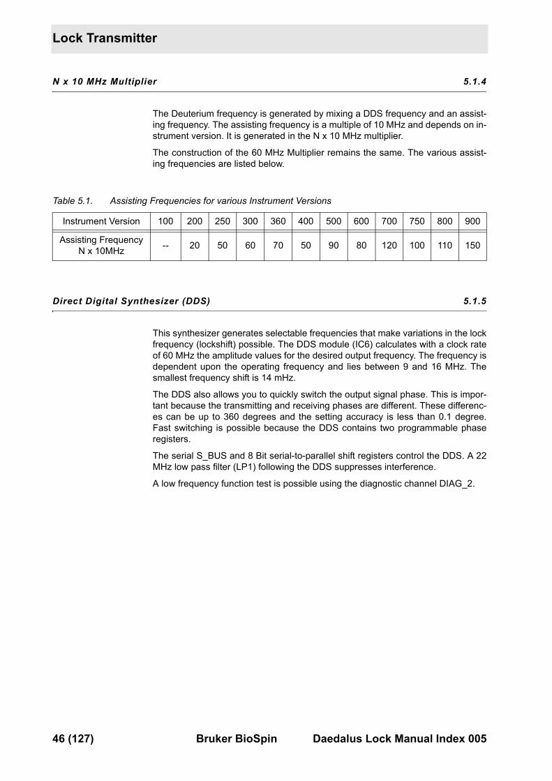
N x 10 MHz Multiplier 5.1.4
The Deuterium frequency is generated by mixing a DDS frequency and an assist-ing frequency. The assisting frequency is a multiple of 10 MHz and depends on in-strument version. It is generated in the N x 10 MHz multiplier.
The construction of the 60 MHz Multiplier remains the same. The various assist-ing frequencies are listed below.
Direct Digital Synthesizer (DDS) 5.1.5
This synthesizer generates selectable frequencies that make variations in the lock frequency (lockshift) possible. The DDS module (IC6) calculates with a clock rate of 60 MHz the amplitude values for the desired output frequency. The frequency is dependent upon the operating frequency and lies between 9 and 16 MHz. The smallest frequency shift is 14 mHz.
The DDS also allows you to quickly switch the output signal phase. This is impor-tant because the transmitting and receiving phases are different. These differenc-es can be up to 360 degrees and the setting accuracy is less than 0.1 degree. Fast switching is possible because the DDS contains two programmable phase registers.
The serial S_BUS and 8 Bit serial-to-parallel shift registers control the DDS. A 22 MHz low pass filter (LP1) following the DDS suppresses interference.
A low frequency function test is possible using the diagnostic channel DIAG_2.
Table 5.1. Assisting Frequencies for various Instrument Versions
Instrument Version 100 200 250 300 360 400 500 600 700 750 800 900
Assisting FrequencyN x 10MHz -- 20 50 60 70 50 90 80 120 100 110 150
46 (127) Bruker BioSpin Daedalus Lock Manual Index 005
Function Description
Quadrature Mixer 5.1.6
The Deuterium frequency is generated in the quadrature mixer from the DDS and the assisting frequency N x 10 MHz. Quadrature mixing suppresses the image frequency and allows superior filtration.
The N x 10 MHz signal and the DDS signal are split in two 0 - 90 degree power splitters and mixed in two active mixers (M6 and M7). Their outputs are added to-gether via the repeating coil TRF4. The 90 degree phase shift of N x 10 MHz is conducted with a lowpass filter (with L18) and a highpass filter (with C131). A broad band solution with 2 repeating coils (TRF2 and 3) is necessary for the DDS signal.
The image rejection is optimized with a potentiometer POT1 and the trimmable condenser C158. The N x 10 MHz frequency can be optimally suppressed by trim-ming potentiometer POT4. (Version ECL01: N x 10 MHz is suppressed by trim-ming the two condenser C174 and C175)
The mixer product (Deuterium frequency) is given to the LO-Output via the M3 amplifier and the following attenuator. In addition the LO-Signal is rectified and, as a DC voltage, used for diagnostics via the DIAG_3 connection.
100MHz instrument versionThe 100MHz instrument version doesn’t need an assisting frequency. The Deute-rium frequency is produced directly from the DDS. The quadrature mixer is there-fore also not needed and bridged.
Attenuator and Switching 5.1.7
The two AGC amplifiers (M4 and M5) adjust and switch the transmitter level. Con-trol proceeds over the UAGC voltage. Transmitter power may be varied by 60dB.
The UAGC voltage will toggle according to whether adjusting (low voltage) or switching (higher voltage = 12V) is taking place.
Daedalus Lock Manual Index 005 Bruker BioSpin 47 (127)
Lock Transmitter
Digital-Analog Converter (DAC) 5.1.8
The transmitter level controlling signal is produced in a DAC (IC5). This DAC is controlled by the Serial Bus and IC3 (OP) converts the current output of the DAC into a proportional voltage. The transmitter power range is adjusted via the poten-tiometers POT2 and POT3. Thereafter the transmitter maximum power is first set with POT2 and then the minimum power with POT3. Both of the temperature sen-sors IC31 and IC32 are compensating the transmitter gain temperature drift. IC31 corrects the gain elevation angle drift and IC32 the gain offset drift.
A second DAC (IC1) may be used for switching and is quickly set via a 7 Bit Bus (EPROM_BUS). Because the In and Out Flanking of the transmitter pulse is con-trolled by this DAC the transmitter pulses are able to be generated in different shapes. The different shape forms are stored in the EPROM.
An OP (IC3) adds both of the DAC signals and delivers the control signal UAGC. This is possible because the control voltage UAGC acts in a linear fashion upon the transmitter power. The Zener Diode limits the UAGC to a maximum of 12 V.
PFP / FFA-Mode Switching 5.1.9
The transmitter signal from the AGC amplifier is divided after the amplifier MOD1. One part is used for the X-Option (e.g. 19F); the other part is amplified again in MOD2. In normal lock operation (PFP Mode) the transmitter signal is switched us-ing IC4 and sent via L19 to the transmitter output (J3). Therefore C79, L19 and C119 act as a quarter wave. The print version ECL01 has an additional attenuator between the switch IC4 and L19 to reduce the transmitter signal. Thus the output level at J4 is 10dB less then the level of version ECL00. The rectified transmitter signal may be used for diagnostics via the DIAG_1 connection.
In FFA mode IC4 switches the signal to the FFA amplifier (T7). IC4 is controlled by a TTL signal via the FFA connection. A logic high level switches on the FFA ampli-fier supply voltage.
If there is a lock substance other than Deuterium used the control connection L_SUBST is logic high. This switches the two Deuterium transmitter signals off.
FFA Amplifier 5.1.10
When the system is functioning in FFA (Fourier) mode this amplifier is switched on to provide the necessary increase in transmitter power. The R127 resistor controls the working point of the transistor T7.
During normal PFP Mode the anti-parallel diodes improve the switching suppres-sion and suppress at the same time a loading of the transmitter signal.
On the other hand in FFA mode L19 and C119 are on resonance and don’t load the FFA transmitter pulse.
48 (127) Bruker BioSpin Daedalus Lock Manual Index 005
Function Description
Pulse-Section 5.1.11
All the digital control pulses for the digital lock are created in the pulse section. The pulse banks are saved in two EPROMs (IC28 and IC29). Every lock mode (Reset, FFA, Normal, Diagnostic...) has its own pulse bank. There is a maximum of two kilobytes per pulse bank. The pulse banks are controlled via the shift regis-ter IC27. The shift register is serially loaded from the lock controller board via the P_BNK0...3 connections and opto-couplers (IC16, IC17, IC18).
The pulse section central unit is the PAL (IC14). Here the control signals (P_BNK0...10), the pulsebank pulses, the counter values and the RCP pulses are coordinated.
Using the RCP pulses (RX_BLNK and TX_BLNK) the receiver and transmitter are switched out in normal lock mode (PFP). The two signals are galvanically separat-ed from the lock electronics by an opto-coupler (IC15).
ECL00..ECL01:An 11 Bit counter counts the addresses from 0 to 2K (A0 to A10). The 1MHz counter clock is generated by dividing the 10 MHz reference (IC30). The counter generates the addresses for the EPROMs. A Clear or Preset signal for the counter is generated by the pulse section central unit depending of the selected mode and counter value.
From ECL02 on:An 10 Bit counter counts the addresses from 0 to 1K (A0 to A9). The 1MHz counter clock is generated by dividing the 10 MHz reference (IC30). The counter generates the addresses for the EPROMs. A Clear or Preset signal for the counter is generated by the pulse section central unit depending of the selected mode and counter value.
A10 (MSB of counter values) is controlled by the pulse section central unit. The pulse section central unit divides each pulse bank into two 1K BYTE wide banks. The lower banks 0K..1K -1 contain the pulse waves and transmitter shapes for normal Lock operation.
The upper banks 1K..2K -1 contain the pulse waves and transmitter shapes for operation in the Transmitter Blank mode. Therefore, A10 is a logical AND connec-tion of the TX_BLNK and the Software Transmitter Blank Mode enable. The signal A10 will be named as BLK_PBANK (BLanK PulseBANK) in further transmitter lay-outs.
The transmitter shape is not generated in normal PFP mode when the transmitter blank is on.
Daedalus Lock Manual Index 005 Bruker BioSpin 49 (127)
Lock Transmitter
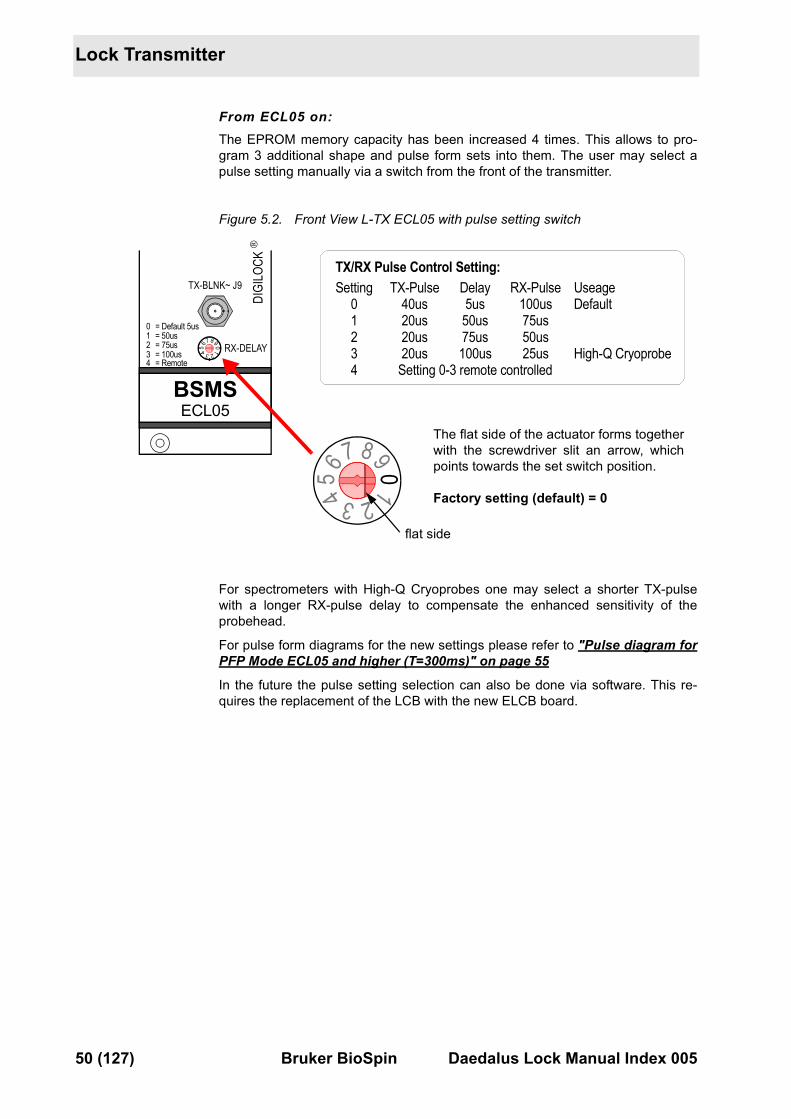
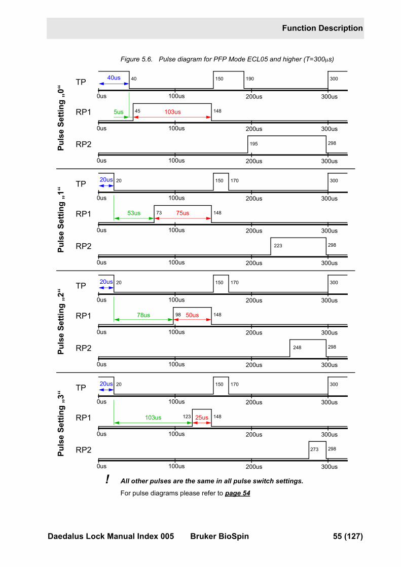
From ECL05 on:The EPROM memory capacity has been increased 4 times. This allows to pro-gram 3 additional shape and pulse form sets into them. The user may select a pulse setting manually via a switch from the front of the transmitter.
Figure 5.2. Front View L-TX ECL05 with pulse setting switch
For spectrometers with High-Q Cryoprobes one may select a shorter TX-pulse with a longer RX-pulse delay to compensate the enhanced sensitivity of the probehead.
For pulse form diagrams for the new settings please refer to "Pulse diagram for PFP Mode ECL05 and higher (T=300ms)" on page 55
In the future the pulse setting selection can also be done via software. This re-quires the replacement of the LCB with the new ELCB board.
05 1
6
2
7
3
8
4
9
TX-BLNK~ J9
BSMSECL05
DIGI
LOCK
�
RX-DELAY10
= 50us= Default 5us
23
= 75us= 100us
4 = Remote
TX-PulseSetting Delay01234
40us20us20us20us
Setting 0-3 remote controlled
5us50us75us100us
TX/RX Pulse Control Setting:RX-Pulse
100us75us50us25us
Default
High-Q Cryoprobe
Useage
05 1
6
2
7
3
8
4
9The flat side of the actuator forms together with the screwdriver slit an arrow, which points towards the set switch position.
Factory setting (default) = 0
flat side
50 (127) Bruker BioSpin Daedalus Lock Manual Index 005
Function Description
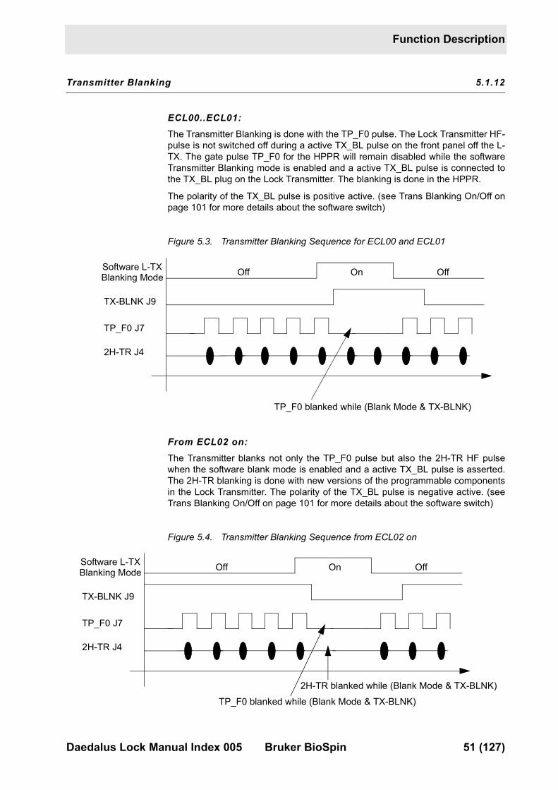
Transmitter Blanking 5.1.12
ECL00..ECL01:The Transmitter Blanking is done with the TP_F0 pulse. The Lock Transmitter HF-pulse is not switched off during a active TX_BL pulse on the front panel off the L-TX. The gate pulse TP_F0 for the HPPR will remain disabled while the software Transmitter Blanking mode is enabled and a active TX_BL pulse is connected to the TX_BL plug on the Lock Transmitter. The blanking is done in the HPPR.
The polarity of the TX_BL pulse is positive active. (see Trans Blanking On/Off on page 101 for more details about the software switch)
Figure 5.3. Transmitter Blanking Sequence for ECL00 and ECL01
From ECL02 on:The Transmitter blanks not only the TP_F0 pulse but also the 2H-TR HF pulse when the software blank mode is enabled and a active TX_BL pulse is asserted. The 2H-TR blanking is done with new versions of the programmable components in the Lock Transmitter. The polarity of the TX_BL pulse is negative active. (see Trans Blanking On/Off on page 101 for more details about the software switch)
Figure 5.4. Transmitter Blanking Sequence from ECL02 on
2H-TR J4
TX-BLNK J9
TP_F0 J7
Software L-TXBlanking Mode Off On Off
TP_F0 blanked while (Blank Mode & TX-BLNK)
2H-TR J4
TX-BLNK J9
TP_F0 J7
Software L-TXBlanking Mode Off On Off
TP_F0 blanked while (Blank Mode & TX-BLNK)2H-TR blanked while (Blank Mode & TX-BLNK)
Daedalus Lock Manual Index 005 Bruker BioSpin 51 (127)
Lock Transmitter
HPPR Gating Pulse TP-F0 5.1.13
The 2H or 19F HF transmit pulse is gated in the HPPR using the TP-F0 pulse.
ECL00..01The TP-F0 is positive active and may be blanked when the Lock Transmitter Blanking mode is asserted.)
From ECL02 on:The TP-F0 Polarity is selectable by the software. The pulse may be either positive or negative active depending on the ECL of the HPPR. The pulse polarity may be configured in the BSMS tool. The TP-F0 may be blanked when the Lock Transmit-ter Blanking mode is asserted.
52 (127) Bruker BioSpin Daedalus Lock Manual Index 005
Function Description
Description of the Most Important Controller Pulses: 5.1.14
From ECL02 on:
CLR~: Reset the Counters
LOAD~: Counter Load Impulse
TP: Lock Electronics Transmitter Pulse
TP_F0: Transmitter Pulse for HP-Preamp, can drive 50 Ohms
RP1, RP2: Receiver Pulse
FFA: Fast Field Adjustment, activates ‘Fast Lock In’
CH_SEL0..2: Address connections for the multiplexer in the Receiver
PHASE_LOAD1: Load Phase 0 in the DDS (Transmitter)
PHASE_LOAD2: Load the selected Lock Phase in the DDS
D_10MHz 10 MHz Clock
PL_CLK: 1 MHz Clock
SHAPE0...6: Blackman Window for Transmitter-Shaping (7 Bit)
ADC_CONV: Conversion pulse for the A/D converter in the Receiver
L_SUBST: Lock Substance (0 = Deuterium, 1 = Option)
RX_BLNK: Receiver Blanking- the Receiver can be switched off using this signal. The signal is galvanically separated from the Lock electronics by an opto-coupler. To enable this input see Rec. Blanking On/Off on page 101.
TX_BLNK: Transmitter Blanking (as above). To enable this input see Trans Blanking On/Off on page 101.
CONT_DATA: Serial Data from the Controller
CONT_WR~: Write Signal for the Serial Bus
CONT_CLK~: Clock for the Serial Bus
CONT_A0...2: Addresses for the Serial Buses that are decoded in IC23 (0=Status Shift Register, 1=Lock Power, 2=DDS, 3=DDS, 4=Lock Gain, 5=PLL for Option)
CONT_DATAR: Connection to read back the serial data for diagnostics
TP_Polarity: Selects polarity of TP_F0 for the HPPR gating. 0 => posi-tive active, 1 => negative active.
PAL_TP_F0: Pulse section out Transmitter Pulse for HP-Preamp. This pulse can be configured by software. PAL_TP_F0 = (TP exor TP_POLARITY)
BLK_PBANK: Transmitter Blank pulse bank selector. BLK_PBANK = (TX-B & TX_CONT)
Daedalus Lock Manual Index 005 Bruker BioSpin 53 (127)
Lock Transmitter
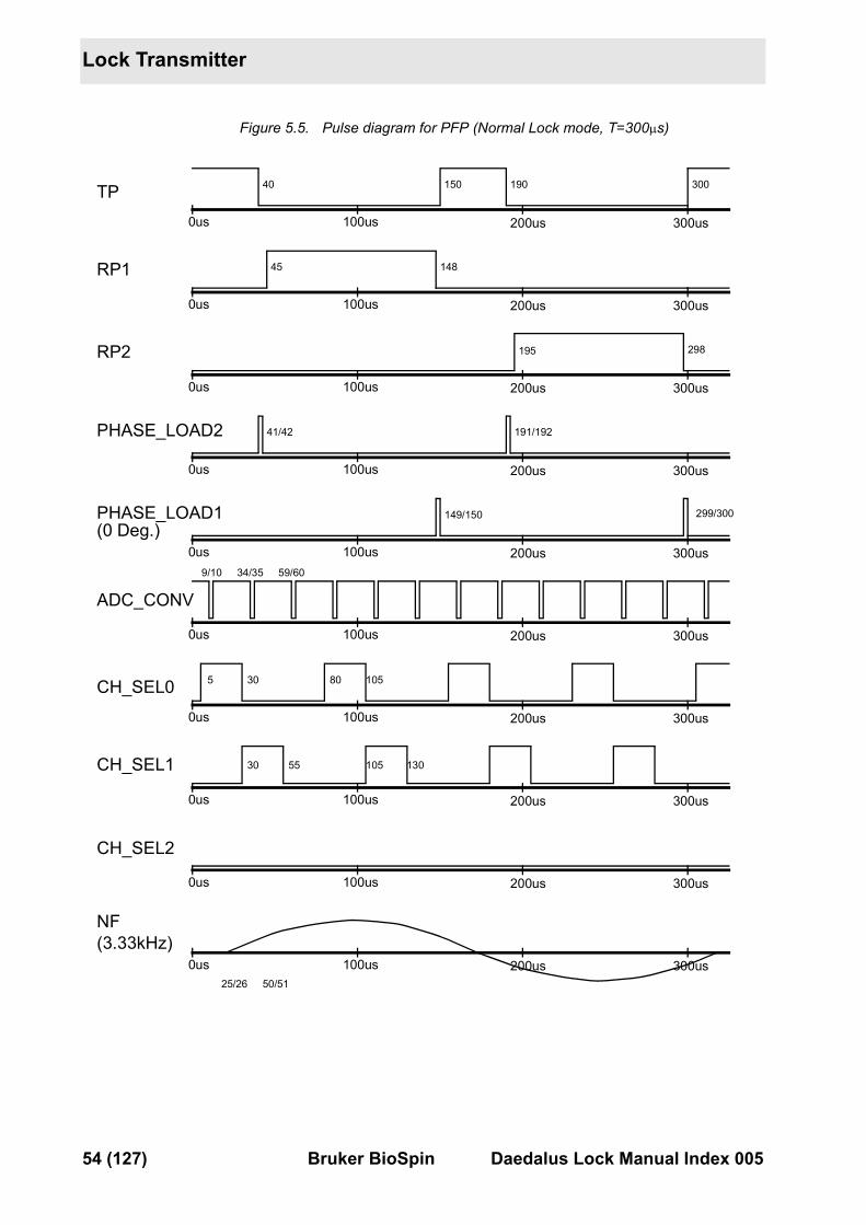
Figure 5.5. Pulse diagram for PFP (Normal Lock mode, T=300�s)
100us 200us 300us0us
100us 200us 300us0us
100us 200us 300us0us
100us 200us 300us0us
100us 200us 300us0us
100us 200us 300us0us
100us 200us 300us0us
100us 200us 300us0us
100us 200us 300us0us
100us 200us 300us0us
TP
RP1
RP2
PHASE_LOAD2
PHASE_LOAD1
ADC_CONV
CH_SEL0
CH_SEL1
CH_SEL2
NF(3.33kHz)
40 150 190 300
45 148
195 298
41/42 191/192
149/150 299/300
9/10 34/35 59/60
5
30
80
105
30
55
105
130
25/26 50/51
(0 Deg.)
54 (127) Bruker BioSpin Daedalus Lock Manual Index 005
Function Description
Figure 5.6. Pulse diagram for PFP Mode ECL05 and higher (T=300�s)
! All other pulses are the same in all pulse switch settings.
For pulse diagrams please refer to page 54
100us 200us 300us0us
100us 200us 300us0us
100us 200us 300us0us
TP
RP1
RP2
40 150 190 300
45 148
195 298
Puls
e Se
tting
„0“
100us 200us 300us0us
100us 200us 300us0us
100us 200us 300us0us
TP
RP1
RP2
20 150 170 300
73 148
223 298
Puls
e Se
tting
„1“
100us 200us 300us0us
100us 200us 300us0us
100us 200us 300us0us
TP
RP1
RP2
20 150 170 300
123 148
273 298
Puls
e Se
tting
„3“
100us 200us 300us0us
100us 200us 300us0us
100us 200us 300us0us
TP
RP1
RP2
20 150 170 300
98 148
248 298
Puls
e Se
tting
„2“
103us
75us
50us
25us
40us
20us
20us
20us
53us
78us
103us
5us
Daedalus Lock Manual Index 005 Bruker BioSpin 55 (127)
Lock Transmitter
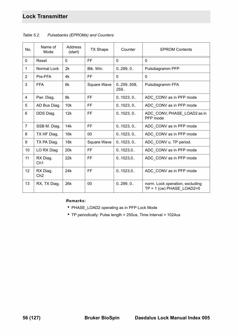
Table 5.2. Pulsebanks (EPROMs) and Counters
Remarks: • PHASE_LOAD2 operating as in PFP Lock Mode
• TP periodically: Pulse length = 250us, Time Interval = 1024us
No. Name of Mode
Address(start) TX Shape Counter EPROM Contents
0 Reset 0 FF 0 0
1 Normal Lock 2k Blk. Win. 0..299, 0.. Pulsdiagramm PFP
2 Pre-FFA 4k FF 0 0
3 FFA 6k Square Wave 0..259..508, 259..
Pulsdiagramm FFA
4 Pwr. Diag. 8k FF 0..1023, 0.. ADC_CONV as in PFP mode
5 AD Bus Diag. 10k FF 0..1023, 0.. ADC_CONV as in PFP mode
6 DDS Diag. 12k FF 0..1023, 0.. ADC_CONV, PHASE_LOAD2 as in PFP mode
7 SSB M. Diag. 14k FF 0..1023, 0.. ADC_CONV as in PFP mode
8 TX HF Diag. 16k 00 0..1023, 0.. ADC_CONV as in PFP mode
9 TX PA Diag. 18k Square Wave 0..1023, 0.. ADC_CONV u. TP period.
10 LO RX Diag 20k FF 0..1023,0.. ADC_CONV as in PFP mode
11 RX Diag. Ch1
22k FF 0..1023,0.. ADC_CONV as in PFP mode
12 RX Diag. Ch2
24k FF 0..1023,0.. ADC_CONV as in PFP mode
13 RX, TX Diag. 26k 00 0..299, 0.. norm. Lock operation, excluding TP = 1 (cw) PHASE_LOAD2=0
56 (127) Bruker BioSpin Daedalus Lock Manual Index 005
Function Description
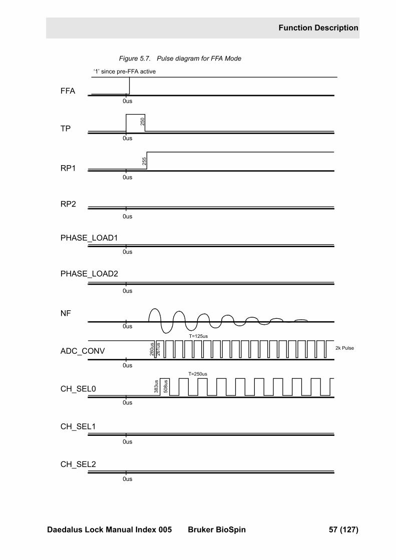
Figure 5.7. Pulse diagram for FFA Mode
‘1’ since pre-FFA active
FFA
TP
RP1
RP2
PHASE_LOAD1
PHASE_LOAD2
NF
ADC_CONV
CH_SEL0
CH_SEL1
CH_SEL2
0us
0us
0us
0us
0us
0us
0us
0us
0us
0us
0us
250
255
383u
s
2k Pulse
T=250us
T=125us
508u
s
260u
s26
1us
Daedalus Lock Manual Index 005 Bruker BioSpin 57 (127)
Lock Transmitter
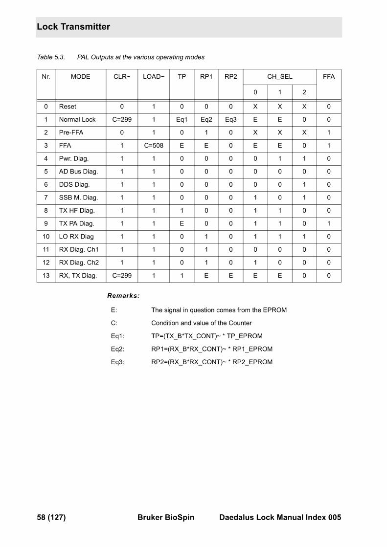
Table 5.3. PAL Outputs at the various operating modes
Remarks:
Nr. MODE CLR~ LOAD~ TP RP1 RP2 CH_SEL FFA
0 1 2
0 Reset 0 1 0 0 0 X X X 0
1 Normal Lock C=299 1 Eq1 Eq2 Eq3 E E 0 0
2 Pre-FFA 0 1 0 1 0 X X X 1
3 FFA 1 C=508 E E 0 E E 0 1
4 Pwr. Diag. 1 1 0 0 0 0 1 1 0
5 AD Bus Diag. 1 1 0 0 0 0 0 0 0
6 DDS Diag. 1 1 0 0 0 0 0 1 0
7 SSB M. Diag. 1 1 0 0 0 1 0 1 0
8 TX HF Diag. 1 1 1 0 0 1 1 0 0
9 TX PA Diag. 1 1 E 0 0 1 1 0 1
10 LO RX Diag 1 1 0 1 0 1 1 1 0
11 RX Diag. Ch1 1 1 0 1 0 0 0 0 0
12 RX Diag. Ch2 1 1 0 1 0 1 0 0 0
13 RX, TX Diag. C=299 1 1 E E E E 0 0
E: The signal in question comes from the EPROM
C: Condition and value of the Counter
Eq1: TP=(TX_B*TX_CONT)~ * TP_EPROM
Eq2: RP1=(RX_B*RX_CONT)~ * RP1_EPROM
Eq3: RP2=(RX_B*RX_CONT)~ * RP2_EPROM
58 (127) Bruker BioSpin Daedalus Lock Manual Index 005
Function Description
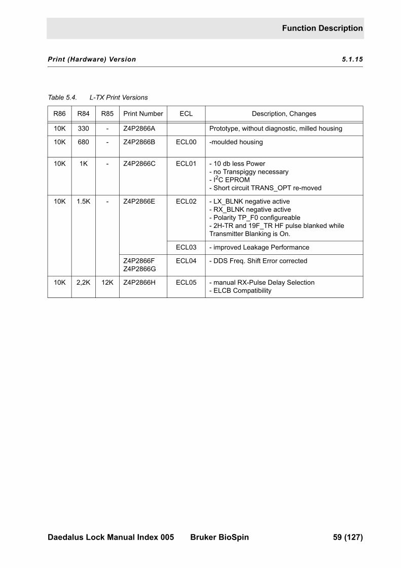
Print (Hardware) Version 5.1.15
Table 5.4. L-TX Print Versions
R86 R84 R85 Print Number ECL Description, Changes
10K 330 - Z4P2866A Prototype, without diagnostic, milled housing
10K 680 - Z4P2866B ECL00 -moulded housing
10K 1K - Z4P2866C ECL01 - 10 db less Power- no Transpiggy necessary- I2C EPROM- Short circuit TRANS_OPT re-moved
10K 1.5K - Z4P2866E ECL02 - LX_BLNK negative active- RX_BLNK negative active- Polarity TP_F0 configureable- 2H-TR and 19F_TR HF pulse blanked while Transmitter Blanking is On.
ECL03 - improved Leakage Performance
Z4P2866FZ4P2866G
ECL04 - DDS Freq. Shift Error corrected
10K 2,2K 12K Z4P2866H ECL05 - manual RX-Pulse Delay Selection- ELCB Compatibility
Daedalus Lock Manual Index 005 Bruker BioSpin 59 (127)

Lock Transmitter
60 (127) Bruker BioSpin Daedalus Lock Manual Index 005
19F TX Option 66000000
Function Description 6.1
0
General 6.1.1
If Fluorine (19F) is used as lock substance, the normal Deuterium lock frequency must be shifted to 19F frequency. This is done in a mixer, which uses a local oscil-lator signal (fpll) and the normal Deuterium signal (f2H) as inputs and creates the 19F frequency (f19F) as output.
This mixing process is performed on the 19F TX Option board. The board also provides the local oscillator signal for the inverse mixing process on the 19F RX Option board, where the Fluorine frequency is shifted back to Deuterium in order to use the normal Deuterium lock receiver path.
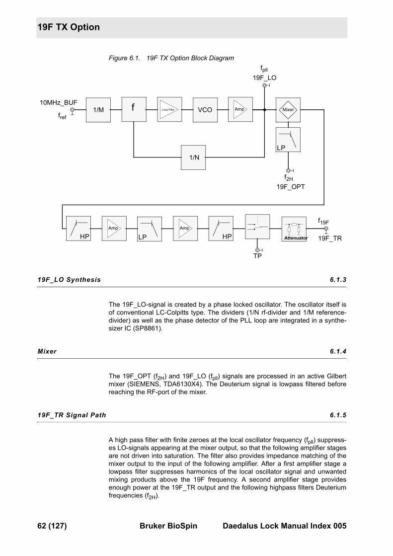
Block Diagram 6.1.2
The block diagram of the lock transmitter gives information about the environment of the 19F TX Option (see "Lock Transmitter" on page 43). A detailed block dia-gram of the 19F TX Option is shown in Figure 6.1.:
f19F fpll f2H��
Daedalus Lock Manual Index 005 Bruker BioSpin 61 (127)
19F TX Option
Figure 6.1. 19F TX Option Block Diagram
19F_LO Synthesis 6.1.3
The 19F_LO-signal is created by a phase locked oscillator. The oscillator itself is of conventional LC-Colpitts type. The dividers (1/N rf-divider and 1/M reference-divider) as well as the phase detector of the PLL loop are integrated in a synthe-sizer IC (SP8861).
Mixer 6.1.4
The 19F_OPT (f2H) and 19F_LO (fpll) signals are processed in an active Gilbert mixer (SIEMENS, TDA6130X4). The Deuterium signal is lowpass filtered before reaching the RF-port of the mixer.
19F_TR Signal Path 6.1.5
A high pass filter with finite zeroes at the local oscillator frequency (fpll) suppress-es LO-signals appearing at the mixer output, so that the following amplifier stages are not driven into saturation. The filter also provides impedance matching of the mixer output to the input of the following amplifier. After a first amplifier stage a lowpass filter suppresses harmonics of the local oscillator signal and unwanted mixing products above the 19F frequency. A second amplifier stage provides enough power at the 19F_TR output and the following highpass filters Deuterium frequencies (f2H).
Mixer
LPHP
VCO1/M
1/N
f Loop Filter
Amp
Amp
HPAmp
fref
10MHz_BUF
f2H
19F_LO
19F_TR
f19F
LP
TP
19F_OPT
fpll
Attenuator
62 (127) Bruker BioSpin Daedalus Lock Manual Index 005
Function Description
A SPDT-bipolar switch controlled by the transmitter pulse (TP) is used to switch off the 19F_TR frequency during acquisition and a resistive attenuator improves VSWR at the 19F_TR output.
19F Lock Operation 6.1.6
• For information about 19F lock operation see "" on page 41.
Daedalus Lock Manual Index 005 Bruker BioSpin 63 (127)
19F TX Option
64 (127) Bruker BioSpin Daedalus Lock Manual Index 005
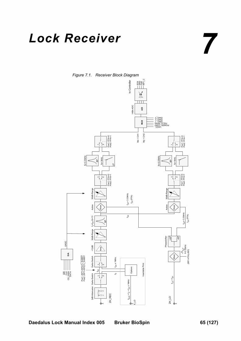
Lock Receiver 77000000
Figure 7.1. Receiver Block Diagram
Mix
er
Mix
er
LP
BP
BP
Amp
A/D
+45o
-45o
MU
X
Mix
er
BP
(RP
1+FF
A)-
RP2
f=3.
33kH
z
2H_L
O
2H_R
EC
30dB
-Ran
ge3d
B-A
ttenu
ator
GaA
s-Sw
itch
+12d
Bf o
=f2H
,Q=1
330
dB-R
ange
fo=3
.33k
Hz
fo=1
kHz
fo=3
.33k
Hz
fo=1
kHz
30dB
-Ran
ge
14Bi
t-AD
C
Pha
sesh
ifter
Activ
e
Activ
eG
aAs-
Sw
itch O
ptio
nsX
_LO
11
22
Pos
1: (R
P1+
RP
2)*L
_SU
BS
T
1 2
1 2
Pos
1: F
FA=0
Pos
2: F
FA=1
Pos
1: F
FA=0
Pos
2: F
FA=1
Pos
1: F
FA=0
Pos
2: F
FA=1
Pos
1: F
FA=0
Pos
2: F
FA=1
11
22
Pos
2: (R
P1+
RP
2)*L
_SU
BS
T
POWER_CONTUAGC
FIELD_SENSDIAG_1DIAG_2DIAG_3
Mx
= C
H1
My
= C
H2
f 2H
± 1
MH
zf X
f LO
= f 2
H
f 2H
f 2H
+ 3.
33kH
z
f 2H
(FFA
)
f 2H
f 2H
+ 3.
33kH
z
f 2H
(FFA
)
SC
KS
RD
FSR
RP
1_C
to C
ontro
ller
D/A
UA
GC
WR
CLK
CS_
GA
IND
ATA
f AU
X =
f X +
f 2H
± 1
MH
z
Inse
rtabl
e P
rint
Daedalus Lock Manual Index 005 Bruker BioSpin 65 (127)
Lock Receiver
Function Description 7.1
0
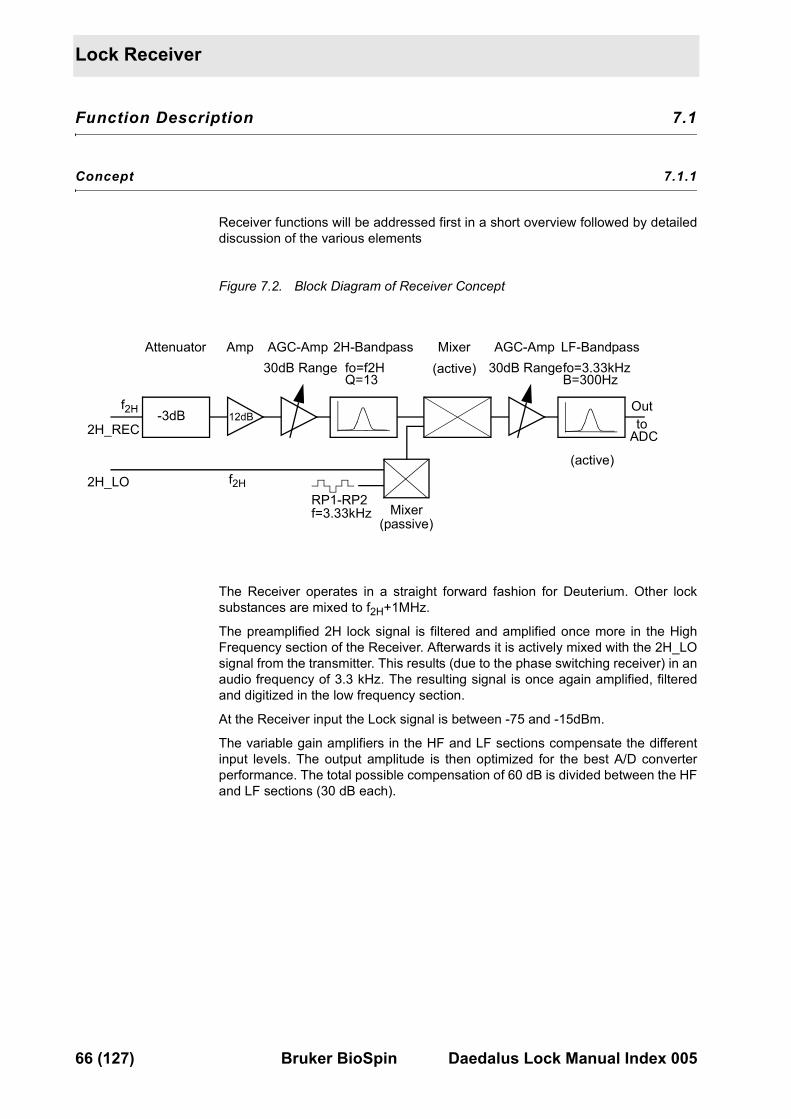
Concept 7.1.1
Receiver functions will be addressed first in a short overview followed by detailed discussion of the various elements
Figure 7.2. Block Diagram of Receiver Concept
The Receiver operates in a straight forward fashion for Deuterium. Other lock substances are mixed to f2H+1MHz.
The preamplified 2H lock signal is filtered and amplified once more in the High Frequency section of the Receiver. Afterwards it is actively mixed with the 2H_LO signal from the transmitter. This results (due to the phase switching receiver) in an audio frequency of 3.3 kHz. The resulting signal is once again amplified, filtered and digitized in the low frequency section.
At the Receiver input the Lock signal is between -75 and -15dBm.
The variable gain amplifiers in the HF and LF sections compensate the different input levels. The output amplitude is then optimized for the best A/D converter performance. The total possible compensation of 60 dB is divided between the HF and LF sections (30 dB each).
Attenuator Amp Mixer AGC-Amp30dB Range
AGC-Amp30dB Range
2H-Bandpass LF-Bandpass
12dB
fo=f2H fo=3.33kHzB=300HzQ=13
Outto
ADC2H_REC-3dB
RP1-RP2f=3.33kHz
2H_LO f2H
f2H
(active)
Mixer(passive)
(active)
66 (127) Bruker BioSpin Daedalus Lock Manual Index 005
Function Description
High Frequency -Section (HF Part) 7.1.2
Attenuator
A 3 dB attenuator at the Receiver input ensures a good matching with the Preamp output.
HF-Amp
Between the attenuator and following variable amplifier stages is a low noise am-plifier. Its job is to keep the noise figure of the whole system low despite the higher noise figure of the following amplifiers. The larger the gain of the previous ele-ments the smaller will be the noise influence of the following stages.The gain is limited by the maximum input signal of the following stages.
HF-Amp with variable Gain
This stage amplifies the signal in the range of 0 to 30 dB (depending on the input level) with very little phase shifting.
HF-Bandpass
A Bandpass (with fo = Deuterium frequency) suppresses disturbing signals from the following mixer. The filter is optimized to a minimum constant group delay, en-suring a short transient time.
Mixer
From here the signal is split into two 90o phase shifted paths to distinguish the dif-ference between absorption and dispersion signals (real and imaginary). As these two paths are identical we will describe just one.
The amplified and filtered Lock signal is mixed at this stage with the 2H_LO-Transmitter Signal. Because phase switching occurs at a clock speed of 6.66 kHz a frequency of 3.33 kHz is found at the mixer output (instead of DC).
Low Frequency Section (LF Section) 7.1.3
LF-Amp with variable Gain
This unit, with a gain range of 30 dB, produces a low frequency signal with con-stant amplitude. This guarantees maximum input range and the best possible res-olution from the D/A converter which follows.
Active Bandpassfilter
To eliminate possible disturbance frequencies and improve the S/N ratio, the low frequency signal is actively filtered before digitization. A choice is made between two filters - a bandpass filter with fo = 3.33 kHz with Q = 10 for normal operation or a lowpass fliter with fo = 0.9 kHz for FFA operation.
Daedalus Lock Manual Index 005 Bruker BioSpin 67 (127)
Lock Receiver
Aquisition 7.1.4
An A/D converter digitizes the absorption and dispersion lock signals alternately and send these serially via the Optocoupler (galvanic isolation) to the Lock Con-troller Board for further processing.
The Multiplexer alternately switches the three low frequency channels (Disper-sions signal, Absorbtions signal, ext. Sensor) to the A/D converter. The sampling rate is 40 kHz. This results in 13.333 kHz per channel which is four times the IF frequency of the receiver.
The digital signals are sent via the 74HC541 driver, the HCPL 2631 optocoupler and the 74HC14 Schmitt-Trigger to the signal processor. The clock is 1 MHz. All components are placed on the receiver board.
Print (Hardware) Version 7.1.5
Table 7.1. L-RX Print Version
R114 R115 R116 Print Number ECL Description
10K 0 -- Z3P2853B Prototype, without diagnostic, milled hous-ing
10K 330 -- Z3P2853C ECL00 moulded housing
10K 680 -- Z3P2853D, E, F, G
ECL01 new mixer, improved leakage and produc-tion performance
68 (127) Bruker BioSpin Daedalus Lock Manual Index 005
19F RX Option 88000000
Function Description 8.1
0
General
In order to lock on to a substance other than Deuterium options must be built into the Receiver and Transmitter.
The descriptions in the this chapter deal with 19F as lock substance.
The Receiver functions as straight forward receiver for Deuterium. To lock on to Fluorine or other substances requires a frequency mixer. The Fluorine frequency (f19F) is created in the transmitter from the Deuterium frequency (f2H) mixed with an auxiliary frequency (fAUX = f2H ± 1MHz + f19F ). Using the same auxiliary fre-quency the Fluorine signal is converted back to the Deuterium frequency range in the receiver option.
The same connection (X_REC) from the preamp to the receiver is used for the 19F-Signal as for the 2H signal. We therefore require switching to the option at the input and output.
Figure 8.1. Signal path in Receiver with built in Option.
Trouble free upgrades to optional lock are available on-site. Upgrading to Fluorine requires alterations to the transmitter as well as the receiver.
AmpX_REC
3dB-Attenuator GaAs-Switch +12dBGaAs-Switch
OptionX_LO
1 1
2 2
Pos1: (RP1+RP2)*L_SUBSTPos2: (RP1+RP2)*L_SUBST
f2H ± 1MHz
fAUX = fX + f2H ± 1MHz
fX
f2H
LOCK_P15VLOCK_AGNDLOCK_AGNDLOCK_AGND
RECEIVER
Daedalus Lock Manual Index 005 Bruker BioSpin 69 (127)
19F RX Option
Concept
The Option has the transfer characteristics of a bandpass filter (see following block diagram). �On the one hand the Lowpass section suppresses the mixer disturbances from the 19F-LO (X_LO) and 19F-RF (X_REC) and on the other hand the highpass section suppresses the 10 MHz reference and other low frequency disturbances. The lower cutoff frequency is 30 MHz (f2H @ 200MHz), while the upper cutoff fre-quency is 115MHz (f2H @ 750MHz). The lowpass is built as a third order filter.
Figure 8.2. X_Option Block Diagram
Mixer
The X_REC and X_LO- signal are processed in a mixer (Mini-Circuit: LRMS 2D) to IF. The capacitor at the RF Input improves the mixer matching for the X_REC Input. X_REC and X_LO are DC coupled.
LRMS_2D data: Conversion Loss: typ. 7.5dB, max 10dB; IF: DC-1000MHz
Attenuator
The attenuator following the mixer matches the mixer to 50 Ohm and suppresses the crosstalk between the LO and the RF path.
Highpass
The second order highpass suppresses the 10 MHz reference and other low fre-quency interference. A 10 MHz signal is suppressed by more than 30 dB. The cut-off frequency is 30 MHz (f2H @ 200MHz).
Buffer Amplifier
The buffer amplifier decouples both the high and low pass filter and compensates the mixer, filter and attenuator losses.
The unit employed is a MSA 0186 from Avantek. Its operating resistance is 560 Ohm. The DC working value of the MSA 0186 is chosen such that the DC voltage at the output is 5V and has a current of 17.8mA. The supply voltage is +15V (LOCK_P15V).
Data for the MSA 0186: Gain: 17dB @ 0.5GHz; Noise Figure: 5.5dB @ 0.5GHz
LPHP
Mixer Amp
DC-BLOCK
X_REC
X_LO
Mixer Attenuator Highpass Buffer Amplifier Lowpass DC-Decouplings
X_IF
0dB@30MHz 0dB@115MHzA=17dBNF=5.5dB
A=-8dB
70 (127) Bruker BioSpin Daedalus Lock Manual Index 005
Connecting the 19F RX-Option
Lowpass FilterThe third order lowpass filter suppresses the 19F-LO (X_LO) and 19F-RF (X_REC) signals. The cutoff frequency is 115MHz. Frequencies below 188MHz (f19F @ 200MHZ) are suppressed by more than 40dB.
DC Decoupling The X_OPTION is DC decoupled with a 10nF condensor.
Print (Hardware) Version 8.1.1
Connecting the 19F RX-Option 8.2
0 The entire X_OPTION/RX (RX: Receiver-Section of the X_OPTION) is a plug in module. Voltage supply, LOCK_P15V and LOCK_AGND are connected by print plugs. The X_REC signals and X_IF are connected directly to the Receiver board with the SMB print connectors. The X_LO signal is connected to the front of the Receiver case on a SMA plug and sent to the X_OPTION/RX via a coaxial cable.
Table 8.1. 19F-RX Option Print Version
R10 R11 Print Number ECL Description
330 -- Z4P2908A ECL00 19F RX-Optin 200..750MHz
Daedalus Lock Manual Index 005 Bruker BioSpin 71 (127)

19F RX Option
72 (127) Bruker BioSpin Daedalus Lock Manual Index 005
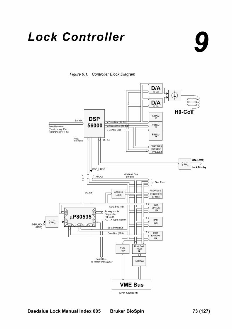
Lock Controller 99000000
Figure 9.1. Controller Block Diagram
H0-Coil
GT01 (X32)
Lock Display
D/A
DSP56000
VME Bus(CPU, Keyboard)
Port 1
Port 2
Port 0
Port 3 Port 4
Port 5
Port 6
RAM
Flash
ADDRESS DECODER
Boot
32k
(EP910)
EPROM128k
EPROM32k
AddressLatch
Dual PortRAM
1k
Latches
VMELogic
Serial Busto / from Transmitter
Analog InputsDiagnostic
Data Bus (8Bit)
up-Control Bus
(16 Bit)
D/A
X RAM2k
Y RAM2k
P RAM
ADDRESS DECODER
Data Bus (8Bit)
TIPAL20L8
16 Bit
16 Bit
Data Bus (24 Bit)
Control Bus
4kSSI TX
SSI RX
from Receiver
HostInterface
A0..A3Address Bus
Adress Bus (16 Bit)(Real-, Imag. Part
D0..D8
DSP_HREQ~
PR-CodeRX, TX Type, Option
DSP_HOLD(RCP)
Test Pins
Reference PP1_C)
�P80535
Daedalus Lock Manual Index 005 Bruker BioSpin 73 (127)
Lock Controller
Function Description 9.1
0
General 9.1.1
The controller is the interface between the Lock’s HF electronics and the BSMS. It receive its instructions for interpretation, completion and confirmation via the VME-Interface.
Microcontroller 9.1.2
The Microcontroller system consists of a 80C535 12 MHz Microcontroller, a 32K * 8 Static RAM, a 32K * 8 EPROM, a 1K * 8 Dual Port RAM, a 128K * 8 Flash EPROM and an EP910 as Addressdecoder. The EPROM contains the Startup and Download software. Applications software is stored in the Flash EPROM. The 80C535 Bus structure consists of a 8 Bit Databus, a 16 Bit address Bus and 5 control connections. In the beginning of a Fetch/Execute sequence the address-latch IC37 latches the addresses A0-A7 with the signal ALE. Port 0 is now changed to function as a data bus for the rest of the sequence (Time multiplexed Portsystem). The System Clock may be generated by the crystal oscillator Q2 (Jumpers 7, 8 on - Jumper 9 off) or be sourced from the BSMS (Jumpers 7, 8 off - Jumper 9 on).
74 (127) Bruker BioSpin Daedalus Lock Manual Index 005
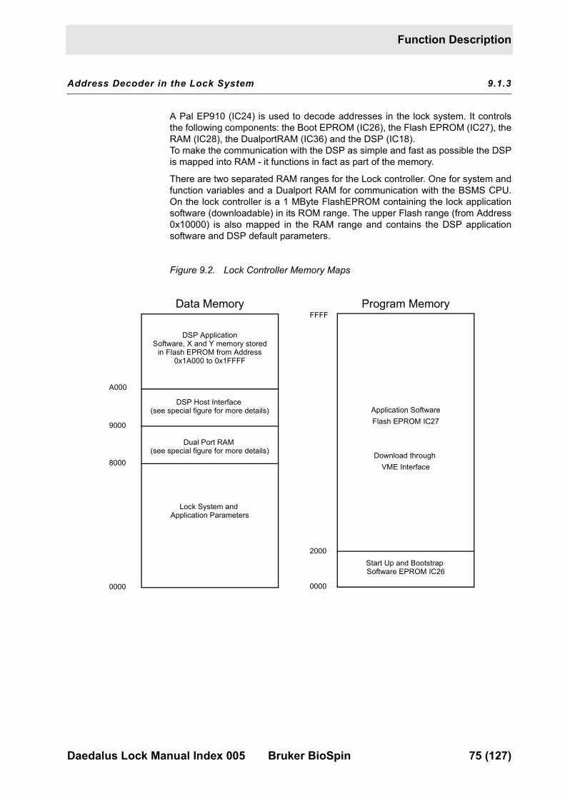
Function Description
Address Decoder in the Lock System 9.1.3
A Pal EP910 (IC24) is used to decode addresses in the lock system. It controls the following components: the Boot EPROM (IC26), the Flash EPROM (IC27), the RAM (IC28), the DualportRAM (IC36) and the DSP (IC18).�To make the communication with the DSP as simple and fast as possible the DSP is mapped into RAM - it functions in fact as part of the memory.
There are two separated RAM ranges for the Lock controller. One for system and function variables and a Dualport RAM for communication with the BSMS CPU. On the lock controller is a 1 MByte FlashEPROM containing the lock application software (downloadable) in its ROM range. The upper Flash range (from Address 0x10000) is also mapped in the RAM range and contains the DSP application software and DSP default parameters.
Figure 9.2. Lock Controller Memory Maps
Data Memory
DSP ApplicationSoftware, X and Y memory stored
in Flash EPROM from Address0x1A000 to 0x1FFFF
DSP Host Interface (see special figure for more details)
Dual Port RAM
Lock System and Application Parameters
(see special figure for more details)
0000
8000
9000
A000
Program Memory
Application SoftwareFlash EPROM IC27
Download through VME Interface
Start Up and Bootstrap Software EPROM IC26
FFFF
0000
2000
Daedalus Lock Manual Index 005 Bruker BioSpin 75 (127)
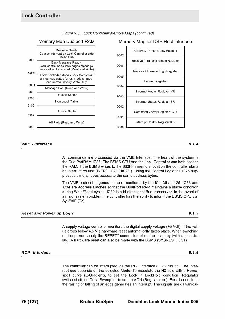
Lock Controller
Figure 9.3. Lock Controller Memory Maps (continued)
VME - Interface 9.1.4
All commands are processed via the VME Interface. The heart of the system is the DualPortRAM IC36. The BSMS CPU and the Lock Controller can both access the RAM. If the BSMS writes to the $83FFh memory location the controller starts an interrupt routine (INTR~, IC23,Pin 23 ). Using the Control Logic the IC25 sup-presses simultaneous access to the same address bytes.
The VME protocol is generated and monitored by the IC’s 35 and 25. IC33 and IC34 are Address Latches so that the DualPort RAM maintains a stable condition during Write/Read cycles. IC32 is a bi-directional Bus transceiver. In the event of a major system problem the controller has the ability to inform the BSMS CPU via �SysFail~ (T2).
Reset and Power up Logic 9.1.5
A supply voltage controller monitors the digital supply voltage (+5 Volt). If the val-ue drops below 4.5 V a hardware reset automatically takes place. When switching on the power supply the RESET~ connection placed on standby (with a time de-lay). A hardware reset can also be made with the BSMS (SYSRES~, IC31).
RCP- Interface 9.1.6
The controller can be interrupted via the RCP Interface (IC23,PIN 32). The Inter-rupt use depends on the selected Mode: To modulate the H0 field with a Homo-spoil curve (Z-Gradient), to set the Lock in LockHold condition (Regulator switched off, no Delta Sweep) or to set LockON (Regulator on). For all conditions the raising or falling of an edge generates an interrupt. The signals are galvanical-
83FF
83FE
83FD
8300
8200
8100
8302
8000
Memory Map Dualport RAM
Message ReadyCauses Interrupt on Lock Controller side
Read Only
Back Message Ready
received and executed (Read and Write)Lock Controller acknowledges message
Lock Controller Mode - Lock Controller announces status (error, mode change
and normal mode): Write Only
Message Pool (Read and Write)
Unused Sector
Homospoil Table
Unused Sector
H0 Field (Read and Write)
9007
9006
9005
9004
9003
9002
9001
9000
Memory Map for DSP Host Interface
Interrupt Vector Register IVR
Interrupt Status Register ISR
Command Vector Register CVR
Interrupt Control Register ICR
Unused Register
Receive / Transmit High Register
Receive / Transmit Middle Register
Receive / Transmit Low Register
76 (127) Bruker BioSpin Daedalus Lock Manual Index 005
Function Description
ly separated with an Optocoupler (IC8). A transistor switch T1 drives the Optocou-pler so that the Bruker norm for threshold switching is adhered to (Logic High = 1 Bruker Volt).
DSP- Host Interface 9.1.7
Communication between the DSP IC18 and the Microcontroller IC23 is achieved with 8 Data Bits, three Address Connections and three Control Connections. The controller has the Host Interface Register mapped in its Data Memory (from Ad-dress 9000h). DSP is selected with DSP_HEN~. The controller chooses the type of access to the DSP with the DSP_HR/W~. The DSP can cause an Interrupt on the controller at any time (DSP_HREQ~, IC23 Pin 24).�After each Power Up or Reset the DSP applications software is loaded via the DSP Host Interface. The DSP keeps its program in the Static RAM IC19.
DSP-Section (Hardware) 9.1.8
The DSP operates in Bootstrap mode. The mode is read in after the Reset with the Pins MODA and MODB. The DSP connection D23 is grounded with a 10k Re-sistor. This leads to the internal Bootstrap Program being activated in DSP after a Reset and the program being loaded via the Host Interface. The data from the Re-ceiver (Dispersion, Absorption and external Field sensor signals) are read into the DSP via the serial sychronized SSI Interface. The display data are sent via the SSI Interface to the graphic terminal (GT01 board in the X32). The entire DSP program is synchronized with the RP1_C pulse via the Interrupt B (negative Edge). External memory MCM56824 (8k*24) is connected at Port A.
The Decoder consists of a 15ns PAL 20L8. The ME~ Signal is decoded here for the memory. The Signals EDAC1~ and EDAC2~ write the data to the Latches (74ACT534 IC12, IC15). The WR~ signal can’t be decoded by the PAL (due to time considerations) and are therefore decoded by fast AC Gates (47AC032). The Most Significant Bit (MSB) is inverted because the DSP delivers the data in two complementing formats (CTC) and the D/A converter also requires the Comple-mentary Offset Binary Format (COB). The converter has its own special 5 V ana-log supply (to reduce disturbance in the converter). The Grounds HO_GND and DGND are connected at DAC (IC17).
RAM OrganizationName Address LocationProgram: (PS~=0) $000..$FFF 0..2k, 4..6kX-Data: (PS~=1, X/Y~=1) $000..$7FF 6..8k Y-Data: (PS~=1, X/Y~=0) $000..$7FF 2..4k
Daedalus Lock Manual Index 005 Bruker BioSpin 77 (127)
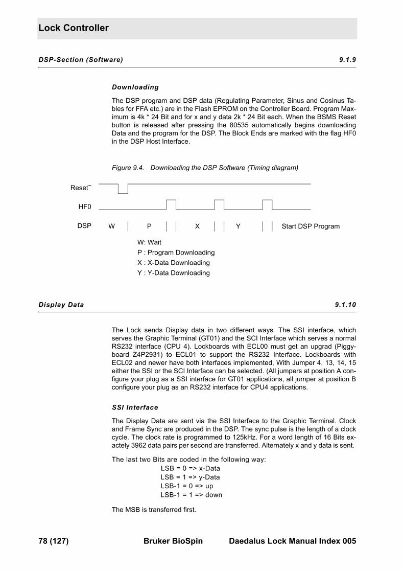
Lock Controller
DSP-Section (Software) 9.1.9
Downloading
The DSP program and DSP data (Regulating Parameter, Sinus and Cosinus Ta-bles for FFA etc.) are in the Flash EPROM on the Controller Board. Program Max-imum is 4k * 24 Bit and for x and y data 2k * 24 Bit each. When the BSMS Reset button is released after pressing the 80535 automatically begins downloading Data and the program for the DSP. The Block Ends are marked with the flag HF0 in the DSP Host Interface.
Figure 9.4. Downloading the DSP Software (Timing diagram)
Display Data 9.1.10
The Lock sends Display data in two different ways. The SSI interface, which serves the Graphic Terminal (GT01) and the SCI Interface which serves a normal RS232 interface (CPU 4). Lockboards with ECL00 must get an upgrad (Piggy-board Z4P2931) to ECL01 to support the RS232 Interface. Lockboards with ECL02 and newer have both interfaces implemented, With Jumper 4, 13, 14, 15 either the SSI or the SCI Interface can be selected. (All jumpers at position A con-figure your plug as a SSI interface for GT01 applications, all jumper at position B configure your plug as an RS232 interface for CPU4 applications.
SSI Interface
The Display Data are sent via the SSI Interface to the Graphic Terminal. Clock and Frame Sync are produced in the DSP. The sync pulse is the length of a clock cycle. The clock rate is programmed to 125kHz. For a word length of 16 Bits ex-actely 3962 data pairs per second are transferred. Alternately x and y data is sent.
The last two Bits are coded in the following way:�LSB = 0 => x-Data�LSB = 1 => y-Data�LSB-1 = 0 => up�LSB-1 = 1 => down
The MSB is transferred first.
Reset~
HF0
DSP W P X Y Start DSP Program
W: WaitP : Program DownloadingX : X-Data DownloadingY : Y-Data Downloading
78 (127) Bruker BioSpin Daedalus Lock Manual Index 005
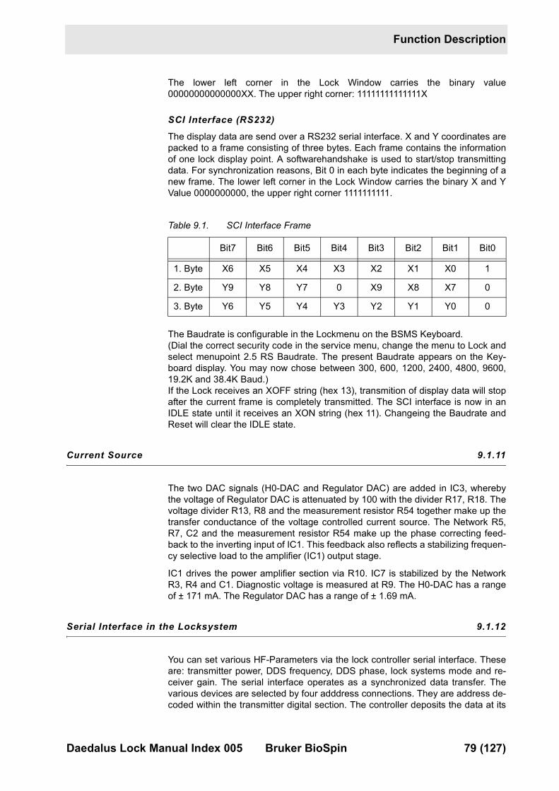
Function Description
The lower left corner in the Lock Window carries the binary value 00000000000000XX. The upper right corner: 11111111111111X
SCI Interface (RS232)
The display data are send over a RS232 serial interface. X and Y coordinates are packed to a frame consisting of three bytes. Each frame contains the information of one lock display point. A softwarehandshake is used to start/stop transmitting data. For synchronization reasons, Bit 0 in each byte indicates the beginning of a new frame. The lower left corner in the Lock Window carries the binary X and Y Value 0000000000, the upper right corner 1111111111.
The Baudrate is configurable in the Lockmenu on the BSMS Keyboard.�(Dial the correct security code in the service menu, change the menu to Lock and select menupoint 2.5 RS Baudrate. The present Baudrate appears on the Key-board display. You may now chose between 300, 600, 1200, 2400, 4800, 9600, 19.2K and 38.4K Baud.)�If the Lock receives an XOFF string (hex 13), transmition of display data will stop after the current frame is completely transmitted. The SCI interface is now in an IDLE state until it receives an XON string (hex 11). Changeing the Baudrate and Reset will clear the IDLE state.
Current Source 9.1.11
The two DAC signals (H0-DAC and Regulator DAC) are added in IC3, whereby the voltage of Regulator DAC is attenuated by 100 with the divider R17, R18. The voltage divider R13, R8 and the measurement resistor R54 together make up the transfer conductance of the voltage controlled current source. The Network R5, R7, C2 and the measurement resistor R54 make up the phase correcting feed-back to the inverting input of IC1. This feedback also reflects a stabilizing frequen-cy selective load to the amplifier (IC1) output stage.
IC1 drives the power amplifier section via R10. IC7 is stabilized by the Network R3, R4 and C1. Diagnostic voltage is measured at R9. The H0-DAC has a range of ± 171 mA. The Regulator DAC has a range of ± 1.69 mA.
Serial Interface in the Locksystem 9.1.12
You can set various HF-Parameters via the lock controller serial interface. These are: transmitter power, DDS frequency, DDS phase, lock systems mode and re-ceiver gain. The serial interface operates as a synchronized data transfer. The various devices are selected by four adddress connections. They are address de-coded within the transmitter digital section. The controller deposits the data at its
Table 9.1. SCI Interface Frame
Bit7 Bit6 Bit5 Bit4 Bit3 Bit2 Bit1 Bit0
1. Byte X6 X5 X4 X3 X2 X1 X0 1
2. Byte Y9 Y8 Y7 0 X9 X8 X7 0
3. Byte Y6 Y5 Y4 Y3 Y2 Y1 Y0 0
Daedalus Lock Manual Index 005 Bruker BioSpin 79 (127)
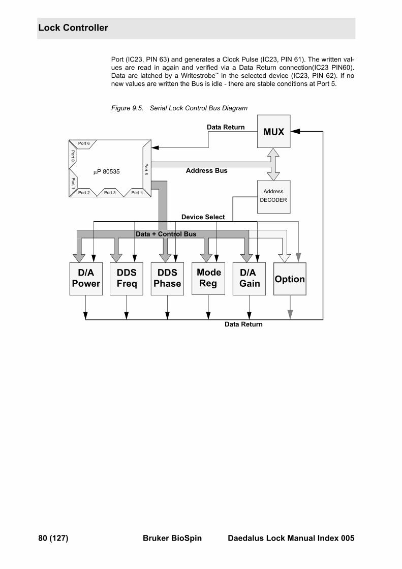
Lock Controller
Port (IC23, PIN 63) and generates a Clock Pulse (IC23, PIN 61). The written val-ues are read in again and verified via a Data Return connection(IC23 PIN60). Data are latched by a Writestrobe~ in the selected device (IC23, PIN 62). If no new values are written the Bus is idle - there are stable conditions at Port 5.
Figure 9.5. Serial Lock Control Bus Diagram
MUX
D/A
Port 1
Port 2
Port 0
Port 3 Port 4
Port 5�P 80535
Port 6
D/A DDSFreq
DDSPhase
ModeReg GainPower
Address Bus
Device Select
Data Return
Data Return
Data + Control Bus
Option
AddressDECODER
80 (127) Bruker BioSpin Daedalus Lock Manual Index 005
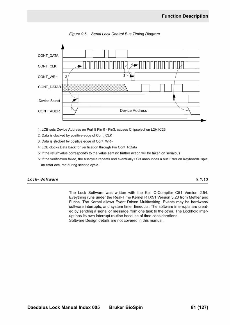
Function Description
Figure 9.6. Serial Lock Control Bus Timing Diagram
Lock- Software 9.1.13
The Lock Software was written with the Keil C-Compiler C51 Version 2.54. Eveything runs under the Real-Time Kernel RTX51 Version 3.20 from Mettler and Fuchs. The Kernel allows Event Driven Multitasking. Events may be hardware/software interrupts, and system timer timeouts. The software interrupts are creat-ed by sending a signal or message from one task to the other. The Lockhold inter-upt has its own interrupt routine because of time considerations. �Software Design details are not covered in this manual.
CONT_DATA
CONT_CLK
CONT_WR~
CONT_DATAR
CONT_ADDR Device Address
Device Select
1
2 3
4
5
1: LCB sets Device Address on Port 5 Pin 0 - Pin3, causes Chipselect on L2H IC232: Data is clocked by positive edge of Cont_CLK3: Data is strobed by positive edge of Cont_WR~
4: LCB clocks Data back for verification through Pin Cont_RData5: If the returnvalue corresponds to the value sent no further action will be taken on serialbus5: If the verification failed, the buscycle repeats and eventually LCB announces a bus Error on KeyboardDisplay
an error occured during second cycle.
Daedalus Lock Manual Index 005 Bruker BioSpin 81 (127)
Lock Controller
Jumper Setting 9.2
0 Jumper settings for board Z4P2859A (ECL00 and 01):
The inscription of JU9 and JU11 on the board shoud be exchanged.
• JU3: always on
• JU4: always on
• JU5: always on
• JU6: on, Download jumper, if this jumper is set the microcontroller system has access to the Boot EPROM and the application software Flash EPROM.�Not set, the microcontroller system access only to the Boot EPROM, the sys-tem is ready for downloading. Remove this jumper if your LCB is in a state which makes normal downloading impossible. Insert it again after completion of download (Your system won’t work until this jumper is inserted again)
• JU9, JU10: on Clock jumper, if the uC clock is generated on board (quarz Q2) set jumper JU9 and JU10 (mind wrong silk screen printing, JU 9 � JU 11)
• JU11: off Clock jumper, if the uC clock is BSMS wide generated and connected to each board, set JU11 and take out JU9 and JU10. (mind wrong silk screen printing, JU 9 � JU 11)
Jumper settings for board Z4P2859B (and C) ECL02:
Two inscriptions used for jumpers, JU and J. JU is not equal to J (JU4 � J4)
• JU3: always on
• JU4: always on
• JU5: always on
• JU6: on, Download jumper, if this jumper is set the microcontroller system has access to the Boot EPROM and the application software Flash EPROM.�Not set, the microcontroller system access only to the Boot EPROM, the sys-tem is ready for downloading. Remove this jumper if your LCB is in a state which makes normal downloading impossible. Insert it again after completion of download (Your system won’t work until this jumper is inserted again)
• JU9, JU10: on Clock jumper, if the uC clock is generated on board (quarz Q2) set jumper JU9 and JU10 (mind wrong silk screen printing, JU9 � JU11)
• JU11: off Clock jumper, if the uC clock is BSMS wide generated and connected to each board, set JU11 and take out JU9 and JU10.
• J4, J13, J14, J15 Display jumpers, this jumpers configure your lock display in-terface. The interface is either SSI or SCI. (see chapter Lock Controller, Dis-play Data for more details) All jumpers at position A configure the interface as SSI for applications with the GT01 board. All jumpers at position B configure the interface as SCI(RS232) for applications with CPU4 uso.�!! Caution Move the four jumpers just blockwide, all at A or all at B !!�If the interface is configured as SCI (all at B), set J10, J11, J12 at position B otherwise no data is transmitted.
• J10, J11, J12 SCI jumpers, this jumpers configure the DSP SCI (serial commu-nication interface) port. All jumpers at position A select the Comp_Bus as SCI driver. All jumpers at position B select the RS232 interface as SCI driver.�!! Caution Move the three jumpers just blockwide, all at A or all at B !!�
82 (127) Bruker BioSpin Daedalus Lock Manual Index 005
Print (Hardware) Version
If the interface is a RS232 interface note that J4, J13, J14 and J15 must be sit-uated at position B.
Print (Hardware) Version 9.3
0
Table 9.2. LCB Print Version
R43 R44 R45 Print Number ECL Description
10K 0 Z4P2859 Prototype, without H0 diagnostic
10K 330 Z4P2859A ECL00
10K 680 Z4P2859A &Z4P2931
ECL01 Piggy Board for RS232-Interface
10K 1K Z4P2859B and Index C
ECL02 -DSP Flat Pack-RS232 Interface-2MBit Flash-Can be upgraded with Z0-Comp.
10K 1K Z4P2859B and Index C
ECL03 -R78,79,80 have been changed to 100 Ohms, the impedance of the RS232 control signals was to high.
10K 1.5K Z4P2859B and Index C
ECL04 -Lock Hold interface hardware chan-ged to negative active, see chapter: Hold Interface for AVANCE Spectrome-ters on page 87
10K 1.8K Z4P2859B and Index C
ECL05 - DSP 33MHz Flat Pack�- DSP with 29.4912 MHz Systemclock�- TP 100Hz at H0 D/AC for Drift Com-pensation
10K 1.8K Z4P2859B and Index C
ECL05.1 LCB ECL05 with a different address decoding EPLD (LCB0AB03.ZE)
10K 1.8K Z4P2859B and Index C
ECL06 - Serial ADC bus terminated with 1.2K� Pull-down Resistors
10K 4.7K 4.7K Z4P2859B and Index C
ECL07 2MByte uProcessor systemNew real time operating system.New boot- and address decoding devices.
Daedalus Lock Manual Index 005 Bruker BioSpin 83 (127)
Lock Controller
84 (127) Bruker BioSpin Daedalus Lock Manual Index 005
Lock RS232 Piggy Board 1010000000
General 10.1
0 The LCB (ECL00) can be upgraded with the Lock-RS Interface Piggy Board (Z4P2931) to ECL01. The main differnce is the interface for transfering the Dis-play-Datas to the computer. The Display-Datas are now being transfererd in RS232 (or SSI) format and can be processed by any computer fitted with RS232-Interface. The LCB ECL02 is standardly equiped with the RS232 and SSI-Interfac. No piggy-board is required for ECL02. The two interfaces can be selected by jumpers (see chapter ‘Jumper Setting’).
Upgrade to ECL01 10.2
0 The following components on the mainboard should be exchanged:
1. New Frontpanel (Z12284)
2. R44 must be exchanged with a 680 ohm resistor (20734)
The following signals have to be connected with the main board:
1. TP1 (X5V) � TP1 Mainboard
2. TP2 (XGND) � JU7 Mainboard
3. TP3 (RXD) � J2 9A Mainboard
4. TP4 (TXD) � J2 9B Mainboard
5. Connnect flat-band-cable (9 pol) with the Sub-D-Connector on the front panel
6. Exchange BSMS-Label with BSMS ECL01-Label
Daedalus Lock Manual Index 005 Bruker BioSpin 85 (127)
Lock RS232 Piggy Board
Figure 10.1. Connections with the Mainboard
Connect with J2 9B
Connect with J2 9A
Connect with TP1Connect with JU7
86 (127) Bruker BioSpin Daedalus Lock Manual Index 005
Hold Interface for AVANCE Spectrom-eters 11
11000000
Introduction 11.1
0
The polarity of all pulses in the new AVANCE Spectrometers have been changed to negative logic.
AMX, ARX or ASX Spectrometers:
The MCI drives the LOCK Hold interface. All pulses are positive active. The LOCK regulates field disturbances when a low (+0V) is connected to the interface. It stops controlling as soon the MCI pulls the Hold pulse high (+5V).
AVANCE D-Series Spectrometers
The TCU drives the LOCK Hold interface. All pulses are negative active. The LOCK regulates field disturbances when a high (+5V) is connected to the inter-face. It stops controlling as soon the TCU pulls the Hold pulse low (+0V).
The interface is configurable either to A-Series (AMX, ARX) spectrometers or to AVANCE spectrometers. The internal interface hardware avoids unstable states when the LOCK Hold interface is not connected or the signal is temporary high impedance driven.
General Description 11.2
0
Adapting the LOCK Hold interface to positive or negative logic requires a hard- and software upgrade. The new requested software release for LOCK systems in all types of spectrometers is lockaf.hex. The software will be downloaded auto-matically when the latest BSMS release (~may 94) is installed and an autodown-load BSMS is executed. The ECL hardware changes must be done according to the upgrade instruction. �The interface must then be configured with the BSMS tool. (see chapter software configuration)�The input logic levels must correspond to the TTL specifications.
Daedalus Lock Manual Index 005 Bruker BioSpin 87 (127)
Hold Interface for AVANCE Spectrometers
Upgrade to new ECL04 11.3
0 The LCB ECL02 and LCB ECL03 can be upgraded to ECL04. The hardware up-grade is necessary for LOCK systems in AVANCE spectrometers. LCB’s in older spectrometers like ARX, AMX do not need an upgrade, the interfaces matches al-ready with the pulse driving device (MCI).�The new software should be downloaded to all BSMS LOCK boards. It includes some new features (see release notes).�Some AVANCE spectrometers are equiped with inverter boxes. LCB useing the LOCK-HOLD with ECL04 must be disconnected from the inverter box and pluged directly to the TCU outputs.
Caution:
Any connected inverters for the L_Hold pulse must be removed. A AVANCE spec-trometer with a new upgraded LCB and a connected inverter box acts like a BSMS LOCK in AMX or ARX spectrometers.
Software Configuration 11.4
0 The interface can be configured with the BSMS tool. This procedure must be done:
• when a BSMS is new installed
• when a CPU in a BSMS system was exchanged
• when the LCB board is upgraded to new ECL04.
Please make sure that possible hardware inverters for the L_HOLD pulse are re-moved.
Configuration Procedure:
• Start the BSMS tool in a UNIX shell with <bsms>
• Change to submenu b “Board functions LCB...“
• Select A L-Hold Pulse Polarity
• Configure 0 if the BSMS is in an AMX or ARX spectrometer (MCI)
• Configure 1 if the BSMS is in a AVANCE D-series spectrometer (TCU)
• Save the Configuration. Exit the “Board functions LCB...“ menu and change to the 5 “BSMS system functions...“ menu. Execute 2 “Save Configuration to EE-PROM“
The configuration is now saved in the non volatile memory of the BSMS. The Lock configures the interface after a power-up or a hardware reset to the selected spectrometer.
88 (127) Bruker BioSpin Daedalus Lock Manual Index 005
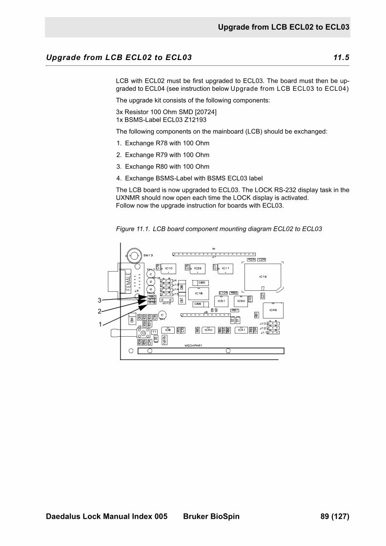
Upgrade from LCB ECL02 to ECL03
Upgrade from LCB ECL02 to ECL03 11.5
0 LCB with ECL02 must be first upgraded to ECL03. The board must then be up-graded to ECL04 (see instruction below Upgrade from LCB ECL03 to ECL04)
The upgrade kit consists of the following components:
3x Resistor 100 Ohm SMD [20724]�1x BSMS-Label ECL03 Z12193
The following components on the mainboard (LCB) should be exchanged:
1. Exchange R78 with 100 Ohm
2. Exchange R79 with 100 Ohm
3. Exchange R80 with 100 Ohm
4. Exchange BSMS-Label with BSMS ECL03 label
The LCB board is now upgraded to ECL03. The LOCK RS-232 display task in the UXNMR should now open each time the LOCK display is activated.�Follow now the upgrade instruction for boards with ECL03.
Figure 11.1. LCB board component mounting diagram ECL02 to ECL03
8 923
1
Daedalus Lock Manual Index 005 Bruker BioSpin 89 (127)
Hold Interface for AVANCE Spectrometers
Upgrade from LCB ECL03 to ECL04 11.6
0 The upgrade kit consists of the following components:
1x self sticky label Z4D5349 L-HOLD~�1x BSMS-Label ECL04 Z12194�3x resistor 0 Ohm [21352]�1x resistor 1.5 kOhm [20739]�1x resistor 2.2 kOhm [20741]�1x resistor 4.7 kOhm [20745]�1x diode 1N914 [22029]
1. Stick label L-HOLD~ over existing L-HOLD labeling at the frontpanel
2. Sxchange BSMS-Label with BSMS ECL04 label
3. Remove R28 56 Ohm
4. Replace R29 with resistor 2.2 kOhm
5. Remove C34
6. Remove C35
7. Replace R32 with diode (mind the polarity, see second diagram). Place the cathode closer to the DSUB9 plug.
8. Replace R30 with resistor 0 Ohm
9. Replace R31 with resistor 0 Ohm
10. Remove T1
11. Replace R55 with resistor 4.7 kOhm
12. Replace R44 with resistor 1.5 kOhm
13. Insert the upgraded LCB board in the BSMS an power up the BSMS
14. Configure the interface with the BSMS tool. (See chapter software configura-tion).
90 (127) Bruker BioSpin Daedalus Lock Manual Index 005
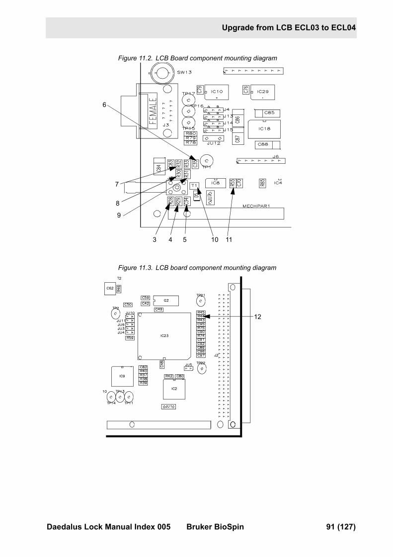
Upgrade from LCB ECL03 to ECL04
Figure 11.2. LCB Board component mounting diagram
Figure 11.3. LCB board component mounting diagram
3 5
7
8
9
104
6
11
12
Daedalus Lock Manual Index 005 Bruker BioSpin 91 (127)
Hold Interface for AVANCE Spectrometers
After the upgrade, the board should look like this.�Check once again the polarity of the inserted diode.
Figure 11.4. LCB Board component mounting after modification
9
Dnew
7
8
114
92 (127) Bruker BioSpin Daedalus Lock Manual Index 005
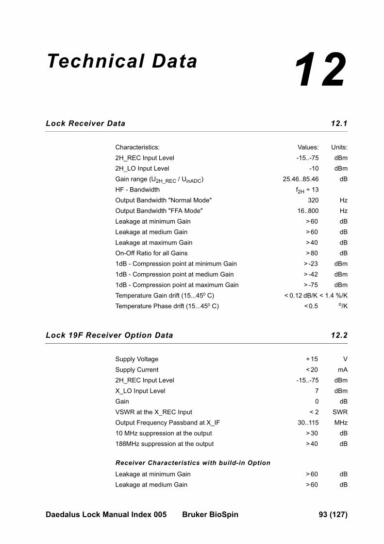
Technical Data 1212000000
Lock Receiver Data 12.1
0 Characteristics: Values: Units:2H_REC Input Level -15..-75 dBm2H_LO Input Level -10 dBmGain range (U2H_REC / UinADC) 25.46..85.46 dBHF - Bandwidth f2H ÷ 13Output Bandwidth "Normal Mode" 320 HzOutput Bandwidth "FFA Mode" 16..800 HzLeakage at minimum Gain > 60 dBLeakage at medium Gain > 60 dBLeakage at maximum Gain > 40 dBOn-Off Ratio for all Gains > 80 dB1dB - Compression point at minimum Gain > -23 dBm1dB - Compression point at medium Gain > -42 dBm1dB - Compression point at maximum Gain > -75 dBmTemperature Gain drift (15...450 C) < 0.12 dB/K < 1.4 %/KTemperature Phase drift (15...450 C) < 0.5 o/K
Lock 19F Receiver Option Data 12.2
0 Supply Voltage + 15 VSupply Current < 20 mA2H_REC Input Level -15..-75 dBmX_LO Input Level 7 dBmGain 0 dBVSWR at the X_REC Input < 2 SWROutput Frequency Passband at X_IF 30..115 MHz10 MHz suppression at the output > 30 dB188MHz suppression at the output > 40 dB
Receiver Characteristics with build-in Option
Leakage at minimum Gain > 60 dBLeakage at medium Gain > 60 dB
Daedalus Lock Manual Index 005 Bruker BioSpin 93 (127)
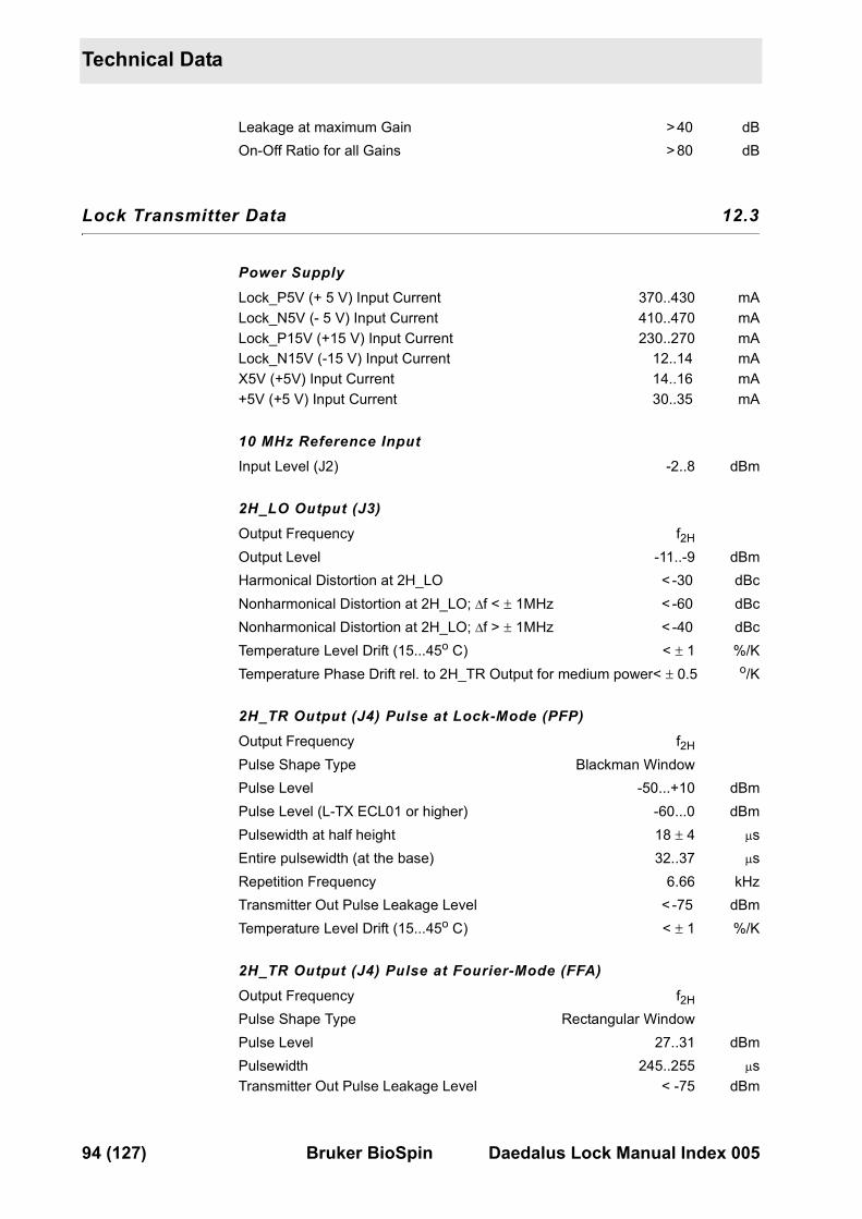
Technical Data
Leakage at maximum Gain > 40 dBOn-Off Ratio for all Gains > 80 dB
Lock Transmitter Data 12.3
0 Power SupplyLock_P5V (+ 5 V) Input Current 370..430 mA�Lock_N5V (- 5 V) Input Current 410..470 mA�Lock_P15V (+15 V) Input Current 230..270 mA�Lock_N15V (-15 V) Input Current 12..14 mA�X5V (+5V) Input Current 14..16 mA�+5V (+5 V) Input Current 30..35 mA
10 MHz Reference InputInput Level (J2) -2..8 dBm
2H_LO Output (J3)Output Frequency f2H
Output Level -11..-9 dBmHarmonical Distortion at 2H_LO < -30 dBcNonharmonical Distortion at 2H_LO; �f < � 1MHz < -60 dBcNonharmonical Distortion at 2H_LO; �f > � 1MHz < -40 dBcTemperature Level Drift (15...45o C) < � 1 %/KTemperature Phase Drift rel. to 2H_TR Output for medium power< � 0.5 o/K
2H_TR Output (J4) Pulse at Lock-Mode (PFP)Output Frequency f2H
Pulse Shape Type Blackman WindowPulse Level -50...+10 dBmPulse Level (L-TX ECL01 or higher) -60...0 dBmPulsewidth at half height 18 � 4 �sEntire pulsewidth (at the base) 32..37 �sRepetition Frequency 6.66 kHzTransmitter Out Pulse Leakage Level < -75 dBmTemperature Level Drift (15...45o C) < � 1 %/K
2H_TR Output (J4) Pulse at Fourier-Mode (FFA)Output Frequency f2H
Pulse Shape Type Rectangular WindowPulse Level 27..31 dBmPulsewidth 245..255 �s �Transmitter Out Pulse Leakage Level < -75 dBm
94 (127) Bruker BioSpin Daedalus Lock Manual Index 005
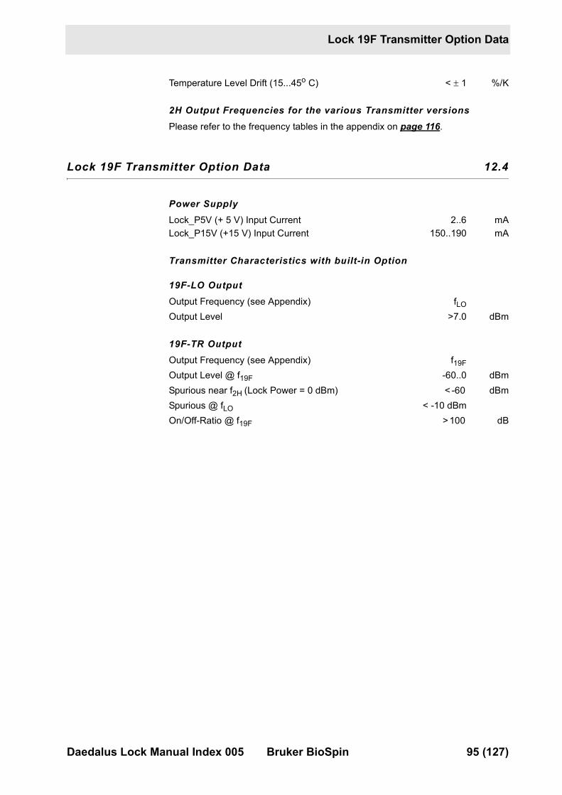
Lock 19F Transmitter Option Data
Temperature Level Drift (15...45o C) < � 1 %/K
2H Output Frequencies for the various Transmitter versionsPlease refer to the frequency tables in the appendix on page 116.
Lock 19F Transmitter Option Data 12.4
0 Power SupplyLock_P5V (+ 5 V) Input Current 2..6 mA�Lock_P15V (+15 V) Input Current 150..190 mA
Transmitter Characteristics with built-in Option
19F-LO OutputOutput Frequency (see Appendix) fLO
Output Level >7.0 dBm
19F-TR OutputOutput Frequency (see Appendix) f19FOutput Level @ f19F -60..0 dBmSpurious near f2H (Lock Power = 0 dBm) < -60 dBmSpurious @ fLO < -10 dBmOn/Off-Ratio @ f19F > 100 dB
Daedalus Lock Manual Index 005 Bruker BioSpin 95 (127)
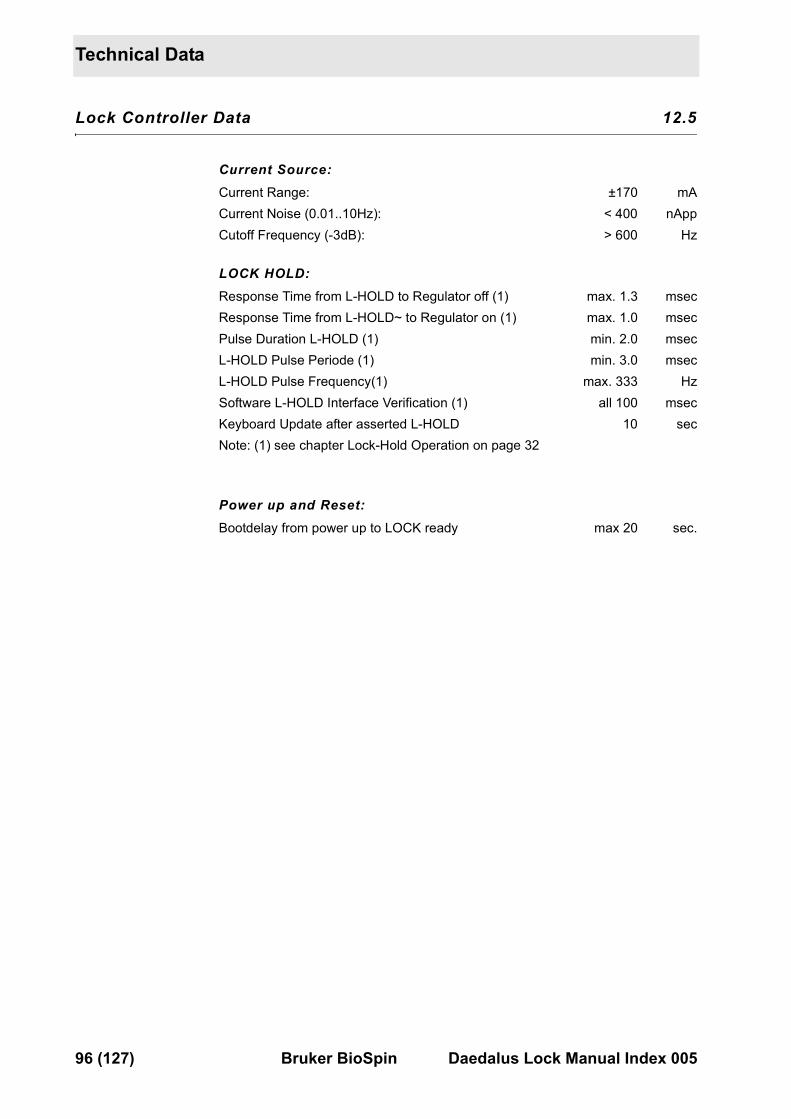
Technical Data
Lock Controller Data 12.5
0 Current Source:Current Range: ±170 mACurrent Noise (0.01..10Hz): < 400 nAppCutoff Frequency (-3dB): > 600 Hz
LOCK HOLD: Response Time from L-HOLD to Regulator off (1) max. 1.3 msecResponse Time from L-HOLD~ to Regulator on (1) max. 1.0 msecPulse Duration L-HOLD (1) min. 2.0 msecL-HOLD Pulse Periode (1) min. 3.0 msecL-HOLD Pulse Frequency(1) max. 333 HzSoftware L-HOLD Interface Verification (1) all 100 msec Keyboard Update after asserted L-HOLD 10 sec Note: (1) see chapter Lock-Hold Operation on page 32
Power up and Reset:Bootdelay from power up to LOCK ready max 20 sec.
96 (127) Bruker BioSpin Daedalus Lock Manual Index 005
Trouble Shooting 1313000000 13000000
Self Test 13.1
0 The self test is automatically activated after each reset. If the self test is success-fully completed on all three lock boards without error detection the green ‘RUN’ LED on the LCB will be lit.
There are two different extension boards helpful and available if you have to make further hardware measurements. They allow you to check the boards out of the BSMS-Rack.
Extension boards for controller testsFor controller tests you need two different extension boards for its two 96-Pin con-nectors. The upper one in the BSMS rack is the VME-Bus and needs a VME-Ex-tension Board (multilayer). A simple one-on-one connection is needed at the lower 96-Pin connector that transmitts the digital control signals.
You may order these two boards with the necessary installation kit at Rotronic AG; Grindelstrasse 6; CH-8303 Bassersdorf; Tel 01/838’11’11 as:
• TESTADAPTER (VME); Part Nr. 20800-191
• TESTADAPTER (1-to-1); Part Nr. 20800-186
• ZWISCHENADAPTER (Inst. Kit); Part Nr. 20800-168
Extension board for receiver and transmitter testsYou may order this extension board at Bruker BioSpin AG; Switzerland:
• BSMS TEST-ADAPTER LOCK Part Nr. Z002746
Daedalus Lock Manual Index 005 Bruker BioSpin 97 (127)

Trouble Shooting
98 (127) Bruker BioSpin Daedalus Lock Manual Index 005
BSMS service tool 14
14000000
The service tool running under UNIX supports more BSMS function than the key-board does. This program can be started by typing ‘bsms‘ under UNIX or by open-ing a shell(!) and typing bsms (!bsms) under UXNMR. Some menupoints affect your system, therefore use them carefully and consider the effects they may have to your lock system.�The lock menu is located at menupoint (B) Board functions LCB.. at the top level of the BSMS service tool (>> Main Menu <<).
Init 14.1
0
The lock initializes itself with its own default values. This values are different than the ‘Save Config’ values after a reset or power up.
DownLoad 14.2
0
This is the manual download feature of new lock application software. Normally BSMS application software is downloaded with the ‘download all boards’ function in the main menu. Download all boards guarantees BSMS software con-sistency. Using the manual download function may cause a not corresponding software configuration at the BSMS. Normally the path for BSMS software is ./bsmssw/
Example: Enter path and name of file to download: bsmssw/lockam.hex
An infostring ‘Erasing Flash EPROM’ indicates that the downloading has be-gun. After the Flash EPROM is erased completely, a linecounter shows the cur-rent state of the download procedure. This counter will raise depending on the software version up to about 4800.
Delete Error 14.3
0
Same function as STD BY on keyboard. The lock displays in case of an error an infostring. As long as this error has not been deleted the lock will remain in an er-rorstate any further operations will be refused. Delete error clears one error in the lock system.
Daedalus Lock Manual Index 005 Bruker BioSpin 99 (127)
BSMS service tool
Version, Config.. 14.4
0
This menupoint gives you useful information about your lock configuration. It shows the type of transmitter and receiver and if any options are plugged into your system.
Lock Substance 14.5
0
This point determines the lock frequency. It sets the lock frequency to a default value (see table Appendix Frequency Generation). It also enables the PLL on the transmitter piggyboard when fluorine option is selected. Since the LOCK SHIFT is in ppm (parts per million of the lock frequency) it also depends on this set-tings.(see D. Lock Shift for more details). After a software upgrade to version lockac (92.02.12), the lock default frequency has to be set to Deuterium (0) and saved with ‘Save Config’ before operation.
A warning is generated after every BSMS powerup or reset if your lock frequency does not equal to the default frequency (Caution Lock Frequency).
Autolock Mode 14.6
0
This is the same function as menu point 2.4 Shift/Field in the lockmenu on key-board.
When Shift/Field is set to ‘0‘(Field) then the Lock Field parameter is adjustable and an autolock routine shifts the H0 Field. The Lock frequency (Lock Shift) is locked and can not be changed.
When Shift/Field is set to ‘1‘(Shift) then the Lock Shift parameter is adjustable and an autolock routine shifts the Lock Transmitter frequency. The Lock Field is locked and can not be changed.
Magnet Type 14.7
0
This point tells to the lock system your magnet type (standard bore, wide bore, su-per wide bore). The lock needs this information for its autolock routines since the magnets have different transfer constants(G/Amp).(see table Technical Data for the H0 Coil and H0 Frequency and Regulating Range for more details).
The Default Value is ‘0‘ equal to standard bore. Write 1 for wide bore and 2 for su-per wide bore magnets.
100 (127) Bruker BioSpin Daedalus Lock Manual Index 005
Trans Blanking On/Off
Trans Blanking On/Off 14.8
0 This functions enables/disables lock transmitter blanking. To blank (no transmitter signal) the transmitter, enable this function and connect plug J9 TX_BLNK at the front panel of L_TX with your blank pulse.
Rec. Blanking On/Off 14.9
0 This functions enables/disables lock receiver blanking. To blank (no receiver ac-quisition) the receiver, enable this function and connect plug J8 RX_BLNK at the front panel of L_TX with your blank pulse.
Lock Hold Pulse Polarity 14.10
0 The Lock Hold interface may be configured to either positive or negative polarity. The appropriate pulse depends on the spectrometer in which the BSMS is in-stalled. The polarity can be set with this function.
Configure ‘0‘ (equals pulse is active high) for a Lock system in an AMX or ARX spectrometer (with a MCI board).
Configure ‘1‘ (equals pulse is active low) for a Lock system in a DMX, DPX , DRX or AV spectrometer (with a TCU board).
The explanation above is not valid for Lock Hold pulses with connected inverter boxes. Remove any inverting components before the configuration of the Hold in-terface.
Make sure that the new configuration is then saved to the non volatile memory in the BSMS CPU (Save Configuration to EEPROM in the BSMS system func-tions menu).
! Important:
The Lock Hold State must be left when the configuration is changed. The Lock software does not accept a new interface configuration while the Hold state is ac-tive. Drive the RCP pulse with the proper logic level before the interface is recon-figured.
For more details see chapter "Lock-Hold Operation" on page 32
Display mode 14.11
0 This is the same function as menupoint Display Mode in the lockmenu on key-board. The lock can display different signals like:
• ‘0‘ real part
• ‘1‘ real part low pass filtered
• ‘2‘ imaginary part
Daedalus Lock Manual Index 005 Bruker BioSpin 101 (127)
BSMS service tool
• ‘3‘ controller out
• ‘4‘ real part expanded (8-times sensitiver than normal real display, sensational for fine shimming)
• ‘5‘ real part expanded low pass filtered
• ‘6‘ FFA spectrum
• ‘7‘ Controller out expanded
• ‘8‘ Lock In Limit
• ‘9‘ inverse sine table
• ‘10‘ inverse cos table
• ‘11‘ regulator diviso
Default value is ‘0‘.
Read Lock Level 14.12
0 This function allows you to read either the MX(0) or MY(1) value.
Lock Shift 14.13
0 This function allows you to work with any desirable lock frequencies. The lock 2H transmitter frequency is generated by mixing a multiple of 10MHz and the DDS frequency, the 19F frequency by mixing a multiple of 10MHz, the DDS freq. and the PPL freq.(a multiple of 1MHz). The controller can load the DDS with frequen-cies up to 20 MHz. The menu Lock Shift has four subfunctions,
• ‘W‘ write a new shift (like the Lock Shift parameter on keyboard), if you want to work with this then the ’Autolock Mode’ (see above) must first be set to ’Shift’.
• ‘R‘ read the current Lock Shift parameter (like the Lock Shift parameter on key-board),
• ‘G‘ read the DDS frequency and display it in Hz,
• ‘O‘ write a new DDS frequency in Hz (Shift value is not taken into consider-ation). This changes the default DDS value and also the frequency variation caused by ‘Lock Shift’ (1ppm � defaultfreq / 1E+06).
Examples 1: Locked with CFCl3 as lock compound. New sample has C6F6 as lock compound. Refer to 19F chemical shift table referenced to CFCl3.
�/ppm for C6F6 is -163 � New Lock Shift is -163ppm(‘W’ 163000).
Example 2: Your 500 Mhz Magnet is 40KHz @ 2H below the standard field. The new 2H de-fault lock frequency is calculated with freq = f2H - 40KHz (Refer to "The follow-ing table contains the recommended ‘new’ Lock-Frequencies. These
102 (127) Bruker BioSpin Daedalus Lock Manual Index 005
Lock Diagnostic
corresponds with the factory configuration of the BSMS. The advantage of this frequency is that in a locked system and a correct set Lock-Shift to the corresponding solvent, the TMS line appears at the exact frequency (for in-stance 500.13000MHz)." on page 117).
f2H for a 500MHz Instrument = 76.774386MHz.
76.774386MHz - 40KHz = 76.734386MHz
Frequency Generation for a 500MHz Instrument: 90MHz - freqDDS (mind the sign!)
New default DDS frequency is 90MHz - 76.734386MHz = 13.265614MHz
Enter 13265614 as new default DDS frequency. Remember that 1ppm (Lock Shift) changes from 76.774386Hz to 76.768244Hz. Save this new configuration with Save Config. in the keyboard service menu. Your lock system is now working as if it was a regular 500MHz system in 2H and 19F applications.
After every BSMS powerup or reset a warning (Caution Lock Frequency) will in-form you about your unusual lock frequency.
Example 3:
Setting the default 2H frequency for all magnets.
Lock Menu � 5. Lock Substance (W)rite ‘0‘ Deuterium. The default frequency is now set as in "The following table contains the recommended ‘new’ Lock-Frequencies. These corresponds with the factory configuration of the BSMS. The advantage of this frequency is that in a locked system and a cor-rect set Lock-Shift to the corresponding solvent, the TMS line appears at the exact frequency (for instance 500.13000MHz)." on page 117. Save this config-uration with Save Config. in the keyboard service menu.
Lock Diagnostic 14.14
0 The lock allows you to run insystem different diagnostic tests. This tests check the system just in a quantity way, that means they will find out that your current source is broken, but they won’t find out a too noisy current source.
Possible checks:
• ‘1‘ Complete self diagnostic, all tests are executed.
• ‘3‘ ADC diagnostic
• ‘4‘ Current Source
• ‘5‘ DDS (Direct Digital Synthesizer) Diagnostic
• ‘6‘ QuadMixer Diagnostic (LO)
• ‘7‘ Transmitter HFSection Diagnostic
• ‘8‘ FFA Amplifier Diagnostic
• ‘9‘ Lock Power Supply Diagnostic
• ‘A‘ Receiver AGC Voltage Diagnostic
The service tool displays the measured value and the range for this diagnostic point. If the value is out of the range an error will appear.
Daedalus Lock Manual Index 005 Bruker BioSpin 103 (127)
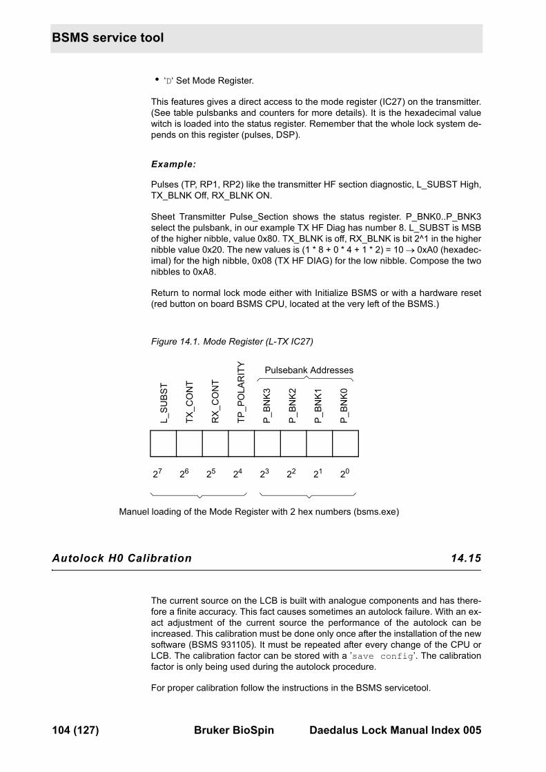
BSMS service tool
• ‘D‘ Set Mode Register.
This features gives a direct access to the mode register (IC27) on the transmitter. (See table pulsbanks and counters for more details). It is the hexadecimal value witch is loaded into the status register. Remember that the whole lock system de-pends on this register (pulses, DSP).
Example:
Pulses (TP, RP1, RP2) like the transmitter HF section diagnostic, L_SUBST High, TX_BLNK Off, RX_BLNK ON.
Sheet Transmitter Pulse_Section shows the status register. P_BNK0..P_BNK3 select the pulsbank, in our example TX HF Diag has number 8. L_SUBST is MSB of the higher nibble, value 0x80. TX_BLNK is off, RX_BLNK is bit 2^1 in the higher nibble value 0x20. The new values is (1 * 8 + 0 * 4 + 1 * 2) = 10 � 0xA0 (hexadec-imal) for the high nibble, 0x08 (TX HF DIAG) for the low nibble. Compose the two nibbles to 0xA8.
Return to normal lock mode either with Initialize BSMS or with a hardware reset (red button on board BSMS CPU, located at the very left of the BSMS.)
Figure 14.1. Mode Register (L-TX IC27)
Autolock H0 Calibration 14.15
0
The current source on the LCB is built with analogue components and has there-fore a finite accuracy. This fact causes sometimes an autolock failure. With an ex-act adjustment of the current source the performance of the autolock can be increased. This calibration must be done only once after the installation of the new software (BSMS 931105). It must be repeated after every change of the CPU or LCB. The calibration factor can be stored with a ’save config’. The calibration factor is only being used during the autolock procedure.
For proper calibration follow the instructions in the BSMS servicetool.
27 26 25 24 23 22 21 20
L_SU
BST
TX_C
ON
T
RX_
CO
NT
P_BN
K0
P_BN
K1
P_BN
K2
P_BN
K3
Pulsebank Addresses
Manuel loading of the Mode Register with 2 hex numbers (bsms.exe)
TP_P
OLA
RIT
Y
104 (127) Bruker BioSpin Daedalus Lock Manual Index 005
Options
Options 14.16
0 Different development and debug tools.
• ‘W’ Load the PLL with a special bitframe.
• ‘X’ load DDS with a special bitframe.
• ‘Y’ Test controller DAC, Testfeature for the controller DAC (IC16).
• ‘0‘ Sets 0, TP 3 = 0V, H0_CURRENT = 0mA
• ‘1‘ Sets +1, TP 3 = 10V, H0_CURRENT = 1.71mA
• ‘2‘ Sets -1, TP 3 = -10V, H0_CURRENT = -1.71mA.
Rewrite the DAC after using with 0!
• ‘Z’ Read only, Locklost parameter.
Save Lock Settings 14.17
0 All lock settings are saved in a file on disk. This includes some parameters which are not part of the BSMS Save Config command. (The only exceptions which are not covered by the BSMS save config command are magnet type, receiver blanking, transmitter blanking and lock substance).
Load Lock Settings 14.18
0 The tool recovers a saved lock setting from a file on disk. This includes some pa-rameter which are not part of the BSMS Init command. (The only exceptions which are not covered by the BSMS save config command are magnet type, re-ceiver blanking, transmitter blanking and lock substance).
RS232 Display Baudrate 14.19
0 This is the same function as menu point RS-Baudrate in the lockmenu on the BSMS keyboard. The lock data is transferred to the CPU/4 CCU via a serial RS232 link. The Baudrate is adjustable to several standard Baudrates.
The RS232 Baudrate generator on the CPU/4 CCU must be initialized with the same baudrate like the BSMS lock.
Default 19200 Baud.
Lock in PWRStep 14.20
0 This is the same function as menupoint Lockin PStep in the lockmenu on the BSMS keyboard. The lock decreases the lock transmitter power parameter when
Daedalus Lock Manual Index 005 Bruker BioSpin 105 (127)
BSMS service tool
the lockin state has been achieved. It increases the lock transmitter power pa-rameter when the lockin state is left.
The magnitude of this power step is adjustable.
Default power step 10dBm.
L-TX TP_F0 Polarity 14.21
0 The Lock transmitter gating pulse for the HPPR preamplifier may be configured to either positive or negative polarity. The selected polarity must match with the preamplifier. Default value: high active.
The polarity selection requests Lock Transmitter ECL02 or newer.
For more details see chapter HPPR Gating Pulse TP-F0 on page 52 of the Daedalus Lock Manual.
106 (127) Bruker BioSpin Daedalus Lock Manual Index 005
Lock Error Messages 1515000000
Error Descriptions 15.1
0 The following Lock error messages may be displayed during start-up or operation of the BSMS.
Table 15.1. Lock Error Messages in alphabetical order
ERROR MESSAGE ERROR DESCRIPTION
SIGNALSNote: Signals of the serial bus (power, gain phase, shift etc.) are only active during a process change
LOCKError 11
Lock boots only from the Boot EPROM (IC26, LCB), there is no applications software in the Flash-EPROM (IC27, LCB). The error may be corrected by loading the lock software.
LOCK Configurable TP-F0 requires L_TX with ECL02 or newerError 169
The TP_F0 pulse is configurable to either positive or negative logic. This requires at least Lock Transmitter with ECL02. The hardware of older L-TX does not support this features.
LOCK DDSFreqBusErrorError 133
Active if a DDS frequency shift could not be loaded correctly. The microprocessor on the lock controller board loads the shift register (IC7, IC8, IC9, IC10) in the Lock Transmitter via a serial bus during a frequency-shift setting. The digital frequency value is read in again by the microprocessor and compared with the transmitted value. If the values are not the same, a LOCK DDS Freq Bus Error is generated.
WR~�
CLK�CS1_DDS�CS2_DDS�DATA LOCK FREQ_RETURN
LOCK DDSPhaseBusErrorError 132
This is displayed if the DDS Phase could not be loaded. The microprocessor on the lock controller board loads the shift register (IC7, IC10) in the Lock Transmitter via a serial bus during a phase setting. The digital phase value is read back in by the microprocessor and compared with the transmitted value. If the values are not the same, a DDS Phase Bus Error is generated.
WR~�
CLK�CS2_DDS�DATA�PHASE_RETURN
LOCK DP_RAMErrorError 15
This means that Read/Write is not possible for one or more memory locations in the Dual Port RAM (IC36 LCB).
Daedalus Lock Manual Index 005 Bruker BioSpin 107 (127)
Lock Error Messages
LOCK DSP Command not acceptedError 167
Communication problems between the uP and the DSP. The software handshake is confused about a inconsistent bus state. You may have to boot the BSMS again if this error appears twice. Please save your BSMS settings with the UXNMR wsh or the “save config“ command in the keyboard.
LOCK DSPDownLoadErrorError 135
Displayed if Downloading is not correctly completed. During Lock Booting the DSP software is loaded into DSP Ram by the microprocessor via the DSP (IC19 on the LCB). After this error several more DSP ERROR messages are displayed but these are of no significance in this instance.
LOCK DSPNoSerialDataError 146
Appears if there is no serial data at the DSP on the lock controller board. The data comes from the Receiver’s A/D converter (IC9).Other possible causes:- The Pulse Section in the transmitter is not working correctly - 10 MHz reference is not connected.Note: Different error messages may appear with the LOCK DSP No Serial Data warning. If this is the case fix the Serial Data problem first and the other message will most likely disappear.
SCK�SRD�
FSRRP1_C�
PL_CLK�HC_10MHZ�ADC_CONV.
LOCK DSP RAM ChecksumError 148
Appears if downloading of the DSP application software was done, but the Microcontroller and the DSP calculated different Checksums Possible Causes:- Failure on the Host Bus, some bits missing at the DSP side- Parts of the DSP Processor system on the LCB do not work correctly (IC18, IC19, IC20)
LCB:uP: A0..A2uP: D0..D7uP: Bus Control SignalsDSP : whole DSP Processor system
LOCK EraseFailError 37
Special algorithms allow an insystem programming of the Flash EPROM. If an erase cycle of a memory location fails, downloading will stop immediately. If this error happens twice, contact your next Bruker service agent or replace board LCB.�To restart the download, reset the BSMS and clear the LOCK Errormessage #11.(The lock uses only the booteprom, no valid application software in its program memory).
LOCK ErrorOnLCBError 4
This is displayed if the CPU, Keyboard or X32 ignore an error that is detected by the Lock and sent to the CPU.
Table 15.1. Lock Error Messages in alphabetical order
ERROR MESSAGE ERROR DESCRIPTION
SIGNALSNote: Signals of the serial bus (power, gain phase, shift etc.) are only active during a process change
108 (127) Bruker BioSpin Daedalus Lock Manual Index 005
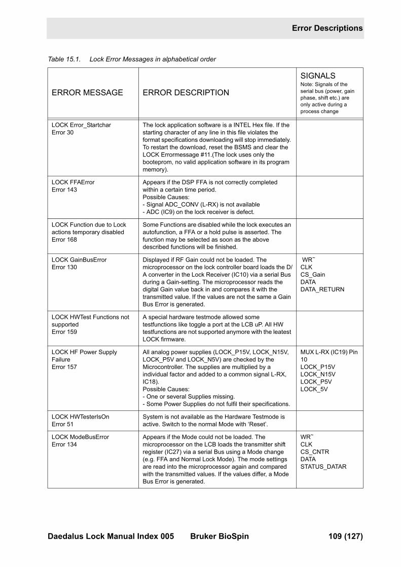
Error Descriptions
LOCK Error_StartcharError 30
The lock application software is a INTEL Hex file. If the starting character of any line in this file violates the format specifications downloading will stop immediately. �To restart the download, reset the BSMS and clear the LOCK Errormessage #11.(The lock uses only the booteprom, no valid application software in its program memory).
LOCK FFAErrorError 143
Appears if the DSP FFA is not correctly completed within a certain time period.Possible Causes:- Signal ADC_CONV (L-RX) is not available- ADC (IC9) on the lock receiver is defect.
LOCK Function due to Lock actions temporary disabledError 168
Some Functions are disabled while the lock executes an autofunction, a FFA or a hold pulse is asserted. The function may be selected as soon as the above described functions will be finished.
LOCK GainBusErrorError 130
Displayed if RF Gain could not be loaded. The microprocessor on the lock controller board loads the D/A converter in the Lock Receiver (IC10) via a serial Bus during a Gain-setting. The microprocessor reads the digital Gain value back in and compares it with the transmitted value. If the values are not the same a Gain Bus Error is generated.
WR~�
CLK�CS_Gain�DATA�DATA_RETURN
LOCK HWTest Functions not supported�Error 159
A special hardware testmode allowed some testfunctions like toggle a port at the LCB uP. All HW testfunctions are not supported anymore with the leatest LOCK firmware.
LOCK HF Power Supply FailureError 157
All analog power supplies (LOCK_P15V, LOCK_N15V, �LOCK_P5V and LOCK_N5V) are checked by the Microcontroller. The supplies are multiplied by a individual factor and added to a common signal L-RX, IC18).Possible Causes:- One or several Supplies missing.- Some Power Supplies do not fulfil their specifications.
MUX L-RX (IC19) Pin 10LOCK_P15VLOCK_N15VLOCK_P5VLOCK_5V
LOCK HWTesterIsOnError 51
System is not available as the Hardware Testmode is active. Switch to the normal Mode with ‘Reset’.
LOCK ModeBusErrorError 134
Appears if the Mode could not be loaded. The microprocessor on the LCB loads the transmitter shift register (IC27) via a serial Bus using a Mode change (e.g. FFA and Normal Lock Mode). The mode settings are read into the microprocessor again and compared with the transmitted values. If the values differ, a Mode Bus Error is generated.
WR~�
CLK�CS_CNTR�
DATA�STATUS_DATAR
Table 15.1. Lock Error Messages in alphabetical order
ERROR MESSAGE ERROR DESCRIPTION
SIGNALSNote: Signals of the serial bus (power, gain phase, shift etc.) are only active during a process change
Daedalus Lock Manual Index 005 Bruker BioSpin 109 (127)
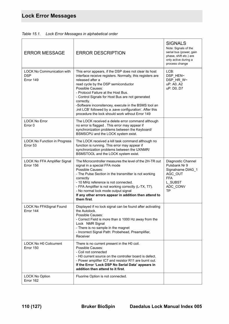
Lock Error Messages
LOCK No Communication with DSPError 149
This error appears, if the DSP does not clear its host interface receive registers. Normally, this registers are released after aread cycle by the DSP semiconductorPossible Causes:- Protocol Failure at the Host Bus.- Control Signals for Host Bus are not generated correctly.-Software inconsitencey, execute in the BSMS tool an ‚init LCB‘ followed by a ‚save configuration‘. After this procedure the lock should work wthout Error 149
LCB:DSP_HEN~DSP_HR_W~uP: A0..A2uP: D0..D7
LOCK No ErrorError 0
The LOCK received a delete error command although no error is flagged . This error may appear if synchronization problems between the Keyboard/BSMSCPU and the LOCK system exist.
LOCK No Function in ProgressError 53
The LOCK received a kill task command although no function is running. This error may appear if synchronization problems between the UXNMR/BSMSTOOL and the LOCK system exist.
LOCK No FFA Amplifier SignalError 156
The Microcontroller measures the level of the 2H-TR out signal in a special FFA modePossible Causes:- The Pulse Section in the transmitter is not working correctly - 10 MHz reference is not connected.- FFA Amplifier is not working correctly (L-TX, T7).- No normal lock mode output signalIf any other errors appear in addition then attend to them first.
Diagnostic ChannelPulsbank Nr 9Signalname DIAG_1AGC_OUTFFAL_SUBSTADC_CONVTP
LOCK No FFASignal FoundError 144
Displayed if no lock signal can be found after activating the Autolock. Possible Causes:- Correct Field is more than ± 1000 Hz away from the Lock NMR Signal- There is no sample in the magnet- Incorrect Signal Path: Probehead, Preamplifier, Receiver
LOCK No H0 CoilcurrentError 150
There is no current present in the H0 coil.Possible Causes:- Coil not connected- H0 current source on the controller board is defect. - Power amplifier IC7 and resistor R11 are burnt out. If the Error ‘Lock DSP No Serial Data’ appears in addition then attend to it first.
LOCK No OptionError 162
Fluorine Option is not connected.
Table 15.1. Lock Error Messages in alphabetical order
ERROR MESSAGE ERROR DESCRIPTION
SIGNALSNote: Signals of the serial bus (power, gain phase, shift etc.) are only active during a process change
110 (127) Bruker BioSpin Daedalus Lock Manual Index 005
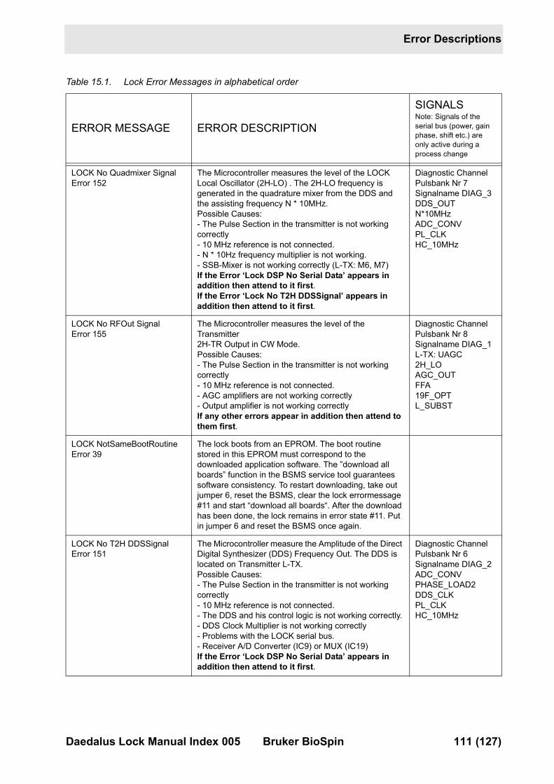
Error Descriptions
LOCK No Quadmixer SignalError 152
The Microcontroller measures the level of the LOCK Local Oscillator (2H-LO) . The 2H-LO frequency is generated in the quadrature mixer from the DDS and the assisting frequency N * 10MHz.Possible Causes:- The Pulse Section in the transmitter is not working correctly - 10 MHz reference is not connected.- N * 10Hz frequency multiplier is not working.- SSB-Mixer is not working correctly (L-TX: M6, M7)If the Error ‘Lock DSP No Serial Data’ appears in addition then attend to it first.If the Error ‘Lock No T2H DDSSignal’ appears in addition then attend to it first.
Diagnostic ChannelPulsbank Nr 7Signalname DIAG_3DDS_OUTN*10MHzADC_CONVPL_CLKHC_10MHz
LOCK No RFOut SignalError 155
The Microcontroller measures the level of the Transmitter �2H-TR Output in CW Mode.Possible Causes:- The Pulse Section in the transmitter is not working correctly - 10 MHz reference is not connected.- AGC amplifiers are not working correctly- Output amplifier is not working correctlyIf any other errors appear in addition then attend to them first.
Diagnostic ChannelPulsbank Nr 8Signalname DIAG_1L-TX: UAGC2H_LOAGC_OUTFFA19F_OPTL_SUBST
LOCK NotSameBootRoutineError 39
The lock boots from an EPROM. The boot routine stored in this EPROM must correspond to the downloaded application software. The ”download all boards” function in the BSMS service tool guarantees software consistency. To restart downloading, take out jumper 6, reset the BSMS, clear the lock errormessage #11 and start “download all boards“. After the download has been done, the lock remains in error state #11. Put in jumper 6 and reset the BSMS once again.
LOCK No T2H DDSSignalError 151
The Microcontroller measure the Amplitude of the Direct Digital Synthesizer (DDS) Frequency Out. The DDS is located on Transmitter L-TX.Possible Causes:- The Pulse Section in the transmitter is not working correctly - 10 MHz reference is not connected.- The DDS and his control logic is not working correctly.- DDS Clock Multiplier is not working correctly- Problems with the LOCK serial bus.- Receiver A/D Converter (IC9) or MUX (IC19)If the Error ‘Lock DSP No Serial Data’ appears in addition then attend to it first.
Diagnostic Channel Pulsbank Nr 6Signalname DIAG_2ADC_CONVPHASE_LOAD2DDS_CLKPL_CLKHC_10MHz
Table 15.1. Lock Error Messages in alphabetical order
ERROR MESSAGE ERROR DESCRIPTION
SIGNALSNote: Signals of the serial bus (power, gain phase, shift etc.) are only active during a process change
Daedalus Lock Manual Index 005 Bruker BioSpin 111 (127)
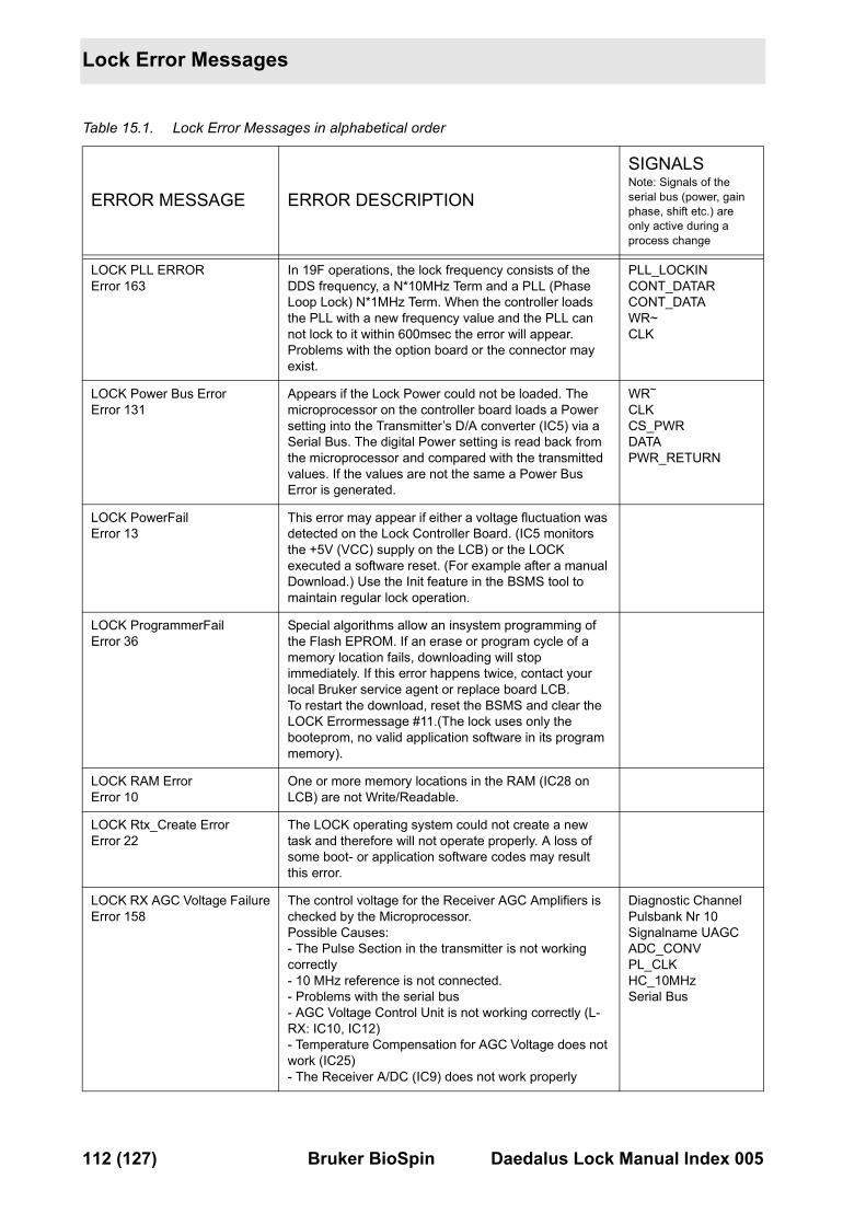
Lock Error Messages
LOCK PLL ERRORError 163
In 19F operations, the lock frequency consists of the DDS frequency, a N*10MHz Term and a PLL (Phase Loop Lock) N*1MHz Term. When the controller loads the PLL with a new frequency value and the PLL can not lock to it within 600msec the error will appear.Problems with the option board or the connector may exist.
PLL_LOCKINCONT_DATARCONT_DATAWR~CLK
LOCK Power Bus ErrorError 131
Appears if the Lock Power could not be loaded. The microprocessor on the controller board loads a Power setting into the Transmitter’s D/A converter (IC5) via a Serial Bus. The digital Power setting is read back from the microprocessor and compared with the transmitted values. If the values are not the same a Power Bus Error is generated.
WR~�
CLK�CS_PWR�
DATA�PWR_RETURN
LOCK PowerFailError 13
This error may appear if either a voltage fluctuation was detected on the Lock Controller Board. (IC5 monitors the +5V (VCC) supply on the LCB) or the LOCK executed a software reset. (For example after a manual Download.) Use the Init feature in the BSMS tool to maintain regular lock operation.
LOCK ProgrammerFailError 36
Special algorithms allow an insystem programming of the Flash EPROM. If an erase or program cycle of a memory location fails, downloading will stop immediately. If this error happens twice, contact your local Bruker service agent or replace board LCB.�To restart the download, reset the BSMS and clear the LOCK Errormessage #11.(The lock uses only the booteprom, no valid application software in its program memory).
LOCK RAM ErrorError 10
One or more memory locations in the RAM (IC28 on LCB) are not Write/Readable.
LOCK Rtx_Create Error Error 22
The LOCK operating system could not create a new task and therefore will not operate properly. A loss of some boot- or application software codes may result this error.
LOCK RX AGC Voltage FailureError 158
The control voltage for the Receiver AGC Amplifiers is checked by the Microprocessor.Possible Causes:- The Pulse Section in the transmitter is not working correctly - 10 MHz reference is not connected.- Problems with the serial bus- AGC Voltage Control Unit is not working correctly (L-RX: IC10, IC12)- Temperature Compensation for AGC Voltage does not work (IC25)- The Receiver A/DC (IC9) does not work properly
Diagnostic ChannelPulsbank Nr 10Signalname UAGCADC_CONVPL_CLKHC_10MHzSerial Bus
Table 15.1. Lock Error Messages in alphabetical order
ERROR MESSAGE ERROR DESCRIPTION
SIGNALSNote: Signals of the serial bus (power, gain phase, shift etc.) are only active during a process change
112 (127) Bruker BioSpin Daedalus Lock Manual Index 005
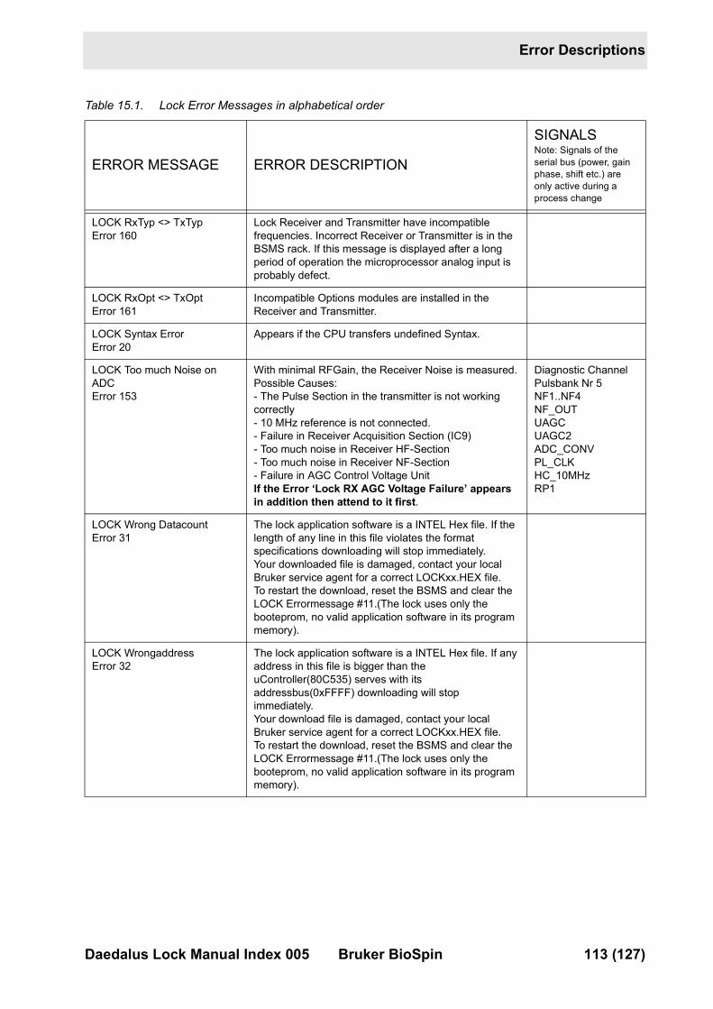
Error Descriptions
LOCK RxTyp <> TxTypError 160
Lock Receiver and Transmitter have incompatible frequencies. Incorrect Receiver or Transmitter is in the BSMS rack. If this message is displayed after a long period of operation the microprocessor analog input is probably defect.
LOCK RxOpt <> TxOptError 161
Incompatible Options modules are installed in the Receiver and Transmitter.
LOCK Syntax ErrorError 20
Appears if the CPU transfers undefined Syntax.
LOCK Too much Noise on ADCError 153
With minimal RFGain, the Receiver Noise is measured.Possible Causes:- The Pulse Section in the transmitter is not working correctly - 10 MHz reference is not connected.- Failure in Receiver Acquisition Section (IC9)- Too much noise in Receiver HF-Section- Too much noise in Receiver NF-Section- Failure in AGC Control Voltage UnitIf the Error ‘Lock RX AGC Voltage Failure’ appears in addition then attend to it first.
Diagnostic ChannelPulsbank Nr 5NF1..NF4NF_OUTUAGCUAGC2ADC_CONVPL_CLKHC_10MHzRP1
LOCK Wrong DatacountError 31
The lock application software is a INTEL Hex file. If the length of any line in this file violates the format specifications downloading will stop immediately. �Your downloaded file is damaged, contact your local Bruker service agent for a correct LOCKxx.HEX file.�To restart the download, reset the BSMS and clear the LOCK Errormessage #11.(The lock uses only the booteprom, no valid application software in its program memory).
LOCK WrongaddressError 32
The lock application software is a INTEL Hex file. If any address in this file is bigger than the uController(80C535) serves with its addressbus(0xFFFF) downloading will stop immediately. �Your download file is damaged, contact your local Bruker service agent for a correct LOCKxx.HEX file.�To restart the download, reset the BSMS and clear the LOCK Errormessage #11.(The lock uses only the booteprom, no valid application software in its program memory).
Table 15.1. Lock Error Messages in alphabetical order
ERROR MESSAGE ERROR DESCRIPTION
SIGNALSNote: Signals of the serial bus (power, gain phase, shift etc.) are only active during a process change
Daedalus Lock Manual Index 005 Bruker BioSpin 113 (127)
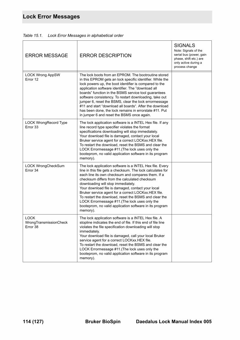
Lock Error Messages
LOCK Wrong AppSWError 12
The lock boots from an EPROM. The bootroutine stored in this EPROM gets an lock specific identifier. While the lock powers up, the boot identifier is compared to the application software identifier. The ”download all boards” function in the BSMS service tool guarantees software consistency. To restart downloading, take out jumper 6, reset the BSMS, clear the lock errormessage #11 and start “download all boards“. After the download has been done, the lock remains in errorstate #11. Put in jumper 6 and reset the BSMS once again.
LOCK WrongRecord TypeError 33
The lock application software is a INTEL Hex file. If any line record type specifier violates the format specifications downloading will stop immediately. �Your download file is damaged, contact your local Bruker service agent for a correct LOCKxx.HEX file.�To restart the download, reset the BSMS and clear the LOCK Errormessage #11.(The lock uses only the booteprom, no valid application software in its program memory).
LOCK WrongCheckSumError 34
The lock application software is a INTEL Hex file. Every line in this file gets a checksum. The lock calculates for each line its own checksum and compares them. If a checksum differs from the calculated checksum downloading will stop immediately. �Your download file is damaged, contact your local Bruker service agent for a correct LOCKxx.HEX file.�To restart the download, reset the BSMS and clear the LOCK Errormessage #11.(The lock uses only the booteprom, no valid application software in its program memory).
LOCK WrongTransmissionCheckError 38
The lock application software is a INTEL Hex file. A stopline indicates the end of file. If this end of file line violates the file specification downloading will stop immediately. �Your download file is damaged, call your local Bruker service agent for a correct LOCKxx.HEX file.�To restart the download, reset the BSMS and clear the LOCK Errormessage #11.(The lock uses only the booteprom, no valid application software in its program memory).
Table 15.1. Lock Error Messages in alphabetical order
ERROR MESSAGE ERROR DESCRIPTION
SIGNALSNote: Signals of the serial bus (power, gain phase, shift etc.) are only active during a process change
114 (127) Bruker BioSpin Daedalus Lock Manual Index 005
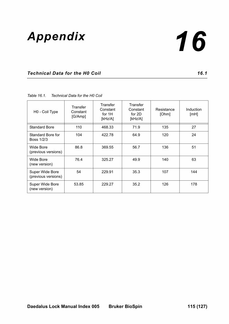
Appendix 1616000000
Technical Data for the H0 Coil 16.1
0
Table 16.1. Technical Data for the H0 Coil
H0 - Coil TypeTransfer Constant[G/Amp]
Transfer Constant
for 1H[kHz/A]
Transfer Constant
for 2D[kHz/A]
Resistance[Ohm]
Induction[mH]
Standard Bore 110 468.33 71.9 135 27
Standard Bore for Boss 1/2/3
104 422.78 64.9 120 24
Wide Bore (previous versions)
86.8 369.55 56.7 136 51
Wide Bore (new version)
76.4 325.27 49.9 140 63
Super Wide Bore (previous versions)
54 229.91 35.3 107 144
Super Wide Bore (new version)
53.85 229.27 35.2 126 178
Daedalus Lock Manual Index 005 Bruker BioSpin 115 (127)
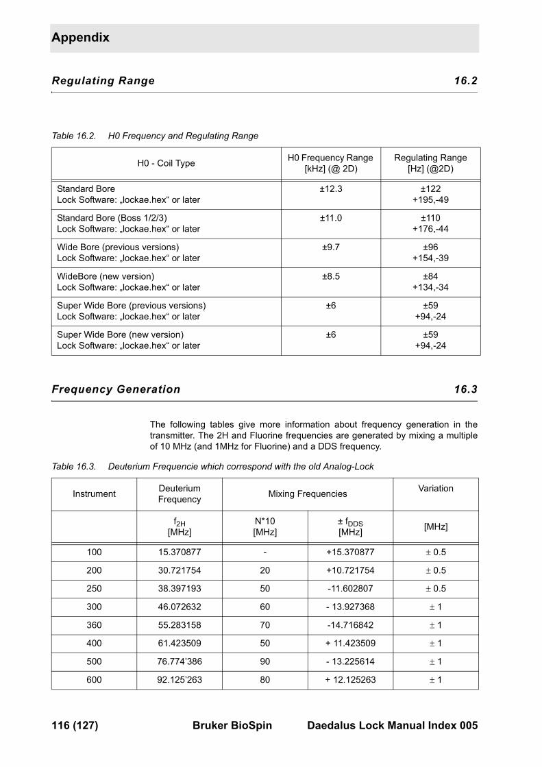
Appendix
Regulating Range 16.2
0
Frequency Generation 16.3
0 The following tables give more information about frequency generation in the transmitter. The 2H and Fluorine frequencies are generated by mixing a multiple of 10 MHz (and 1MHz for Fluorine) and a DDS frequency.
Table 16.2. H0 Frequency and Regulating Range
H0 - Coil Type H0 Frequency Range [kHz] (@ 2D)
Regulating Range [Hz] (@2D)
Standard BoreLock Software: „lockae.hex“ or later
±12.3 ±122+195,-49
Standard Bore (Boss 1/2/3)Lock Software: „lockae.hex“ or later
±11.0 ±110+176,-44
Wide Bore (previous versions)Lock Software: „lockae.hex“ or later
±9.7 ±96+154,-39
WideBore (new version)Lock Software: „lockae.hex“ or later
±8.5 ±84+134,-34
Super Wide Bore (previous versions)Lock Software: „lockae.hex“ or later
±6 ±59+94,-24
Super Wide Bore (new version)Lock Software: „lockae.hex“ or later
±6 ±59+94,-24
Table 16.3. Deuterium Frequencie which correspond with the old Analog-Lock
Instrument Deuterium Frequency Mixing Frequencies Variation
f2H [MHz]
N*10[MHz]
± fDDS[MHz] [MHz]
100 15.370877 - +15.370877 � 0.5
200 30.721754 20 +10.721754 � 0.5
250 38.397193 50 -11.602807 � 0.5
300 46.072632 60 - 13.927368 � 1
360 55.283158 70 -14.716842 � 1
400 61.423509 50 + 11.423509 � 1
500 76.774’386 90 - 13.225614 � 1
600 92.125’263 80 + 12.125263 � 1
116 (127) Bruker BioSpin Daedalus Lock Manual Index 005
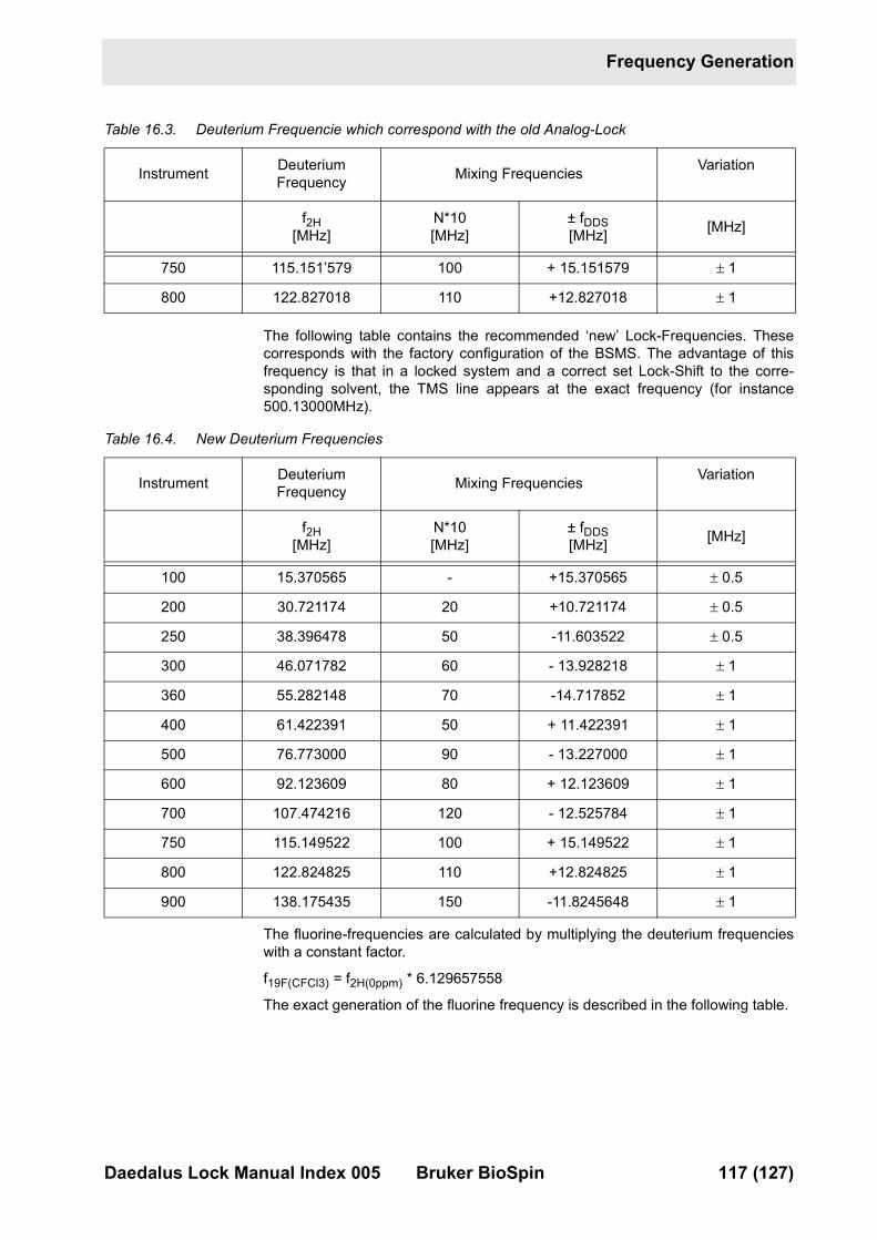
Frequency Generation
The following table contains the recommended ‘new’ Lock-Frequencies. These corresponds with the factory configuration of the BSMS. The advantage of this frequency is that in a locked system and a correct set Lock-Shift to the corre-sponding solvent, the TMS line appears at the exact frequency (for instance 500.13000MHz).
The fluorine-frequencies are calculated by multiplying the deuterium frequencies with a constant factor.
f19F(CFCl3) = f2H(0ppm) * 6.129657558
The exact generation of the fluorine frequency is described in the following table.
750 115.151’579 100 + 15.151579 � 1
800 122.827018 110 +12.827018 � 1
Table 16.4. New Deuterium Frequencies
Instrument Deuterium Frequency Mixing Frequencies Variation
f2H [MHz]
N*10[MHz]
± fDDS[MHz] [MHz]
100 15.370565 - +15.370565 � 0.5
200 30.721174 20 +10.721174 � 0.5
250 38.396478 50 -11.603522 � 0.5
300 46.071782 60 - 13.928218 � 1
360 55.282148 70 -14.717852 � 1
400 61.422391 50 + 11.422391 � 1
500 76.773000 90 - 13.227000 � 1
600 92.123609 80 + 12.123609 � 1
700 107.474216 120 - 12.525784 � 1
750 115.149522 100 + 15.149522 � 1
800 122.824825 110 +12.824825 � 1
900 138.175435 150 -11.8245648 � 1
Table 16.3. Deuterium Frequencie which correspond with the old Analog-Lock
Instrument Deuterium Frequency Mixing Frequencies Variation
f2H [MHz]
N*10[MHz]
± fDDS[MHz] [MHz]
Daedalus Lock Manual Index 005 Bruker BioSpin 117 (127)
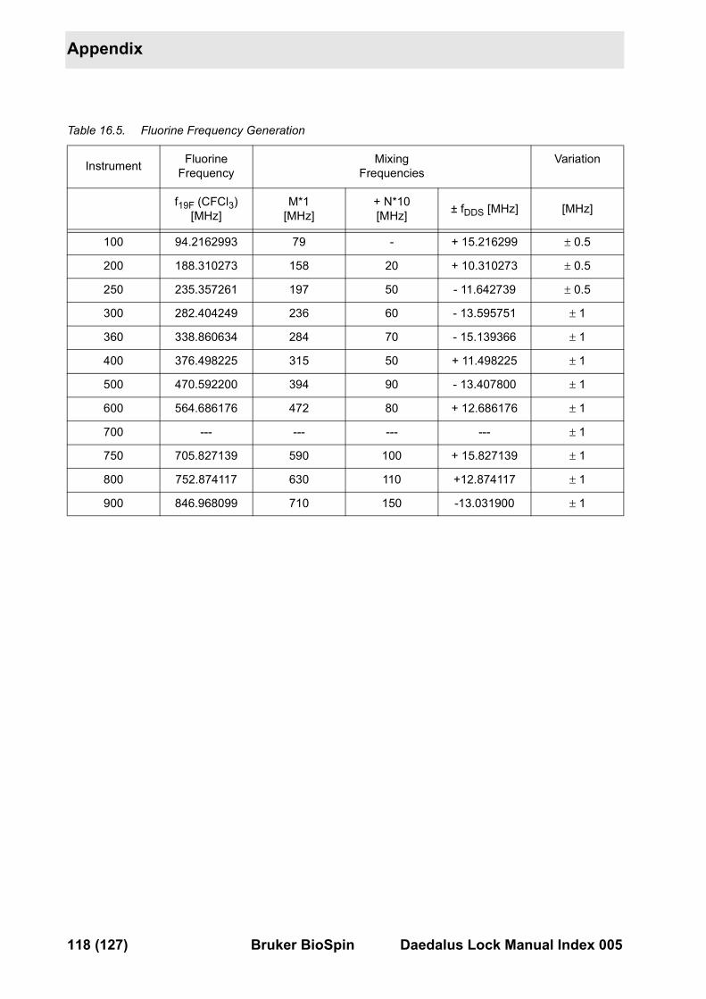
Appendix
Table 16.5. Fluorine Frequency Generation
Instrument Fluorine Frequency
Mixing Frequencies
Variation
f19F (CFCl3)[MHz]
M*1[MHz]
+ N*10[MHz] ± fDDS [MHz] [MHz]
100 94.2162993 79 - + 15.216299 � 0.5
200 188.310273 158 20 + 10.310273 � 0.5
250 235.357261 197 50 - 11.642739 � 0.5
300 282.404249 236 60 - 13.595751 � 1
360 338.860634 284 70 - 15.139366 � 1
400 376.498225 315 50 + 11.498225 � 1
500 470.592200 394 90 - 13.407800 � 1
600 564.686176 472 80 + 12.686176 � 1
700 --- --- --- --- � 1
750 705.827139 590 100 + 15.827139 � 1
800 752.874117 630 110 +12.874117 � 1
900 846.968099 710 150 -13.031900 � 1
118 (127) Bruker BioSpin Daedalus Lock Manual Index 005
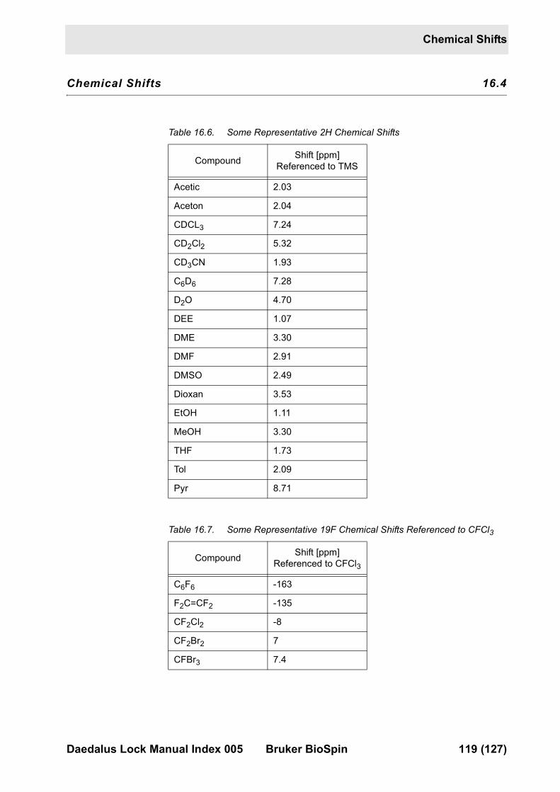
Chemical Shifts
Chemical Shifts 16.4
0
Table 16.6. Some Representative 2H Chemical Shifts
Compound Shift [ppm]Referenced to TMS
Acetic 2.03
Aceton 2.04
CDCL3 7.24
CD2Cl2 5.32
CD3CN 1.93
C6D6 7.28
D2O 4.70
DEE 1.07
DME 3.30
DMF 2.91
DMSO 2.49
Dioxan 3.53
EtOH 1.11
MeOH 3.30
THF 1.73
Tol 2.09
Pyr 8.71
Table 16.7. Some Representative 19F Chemical Shifts Referenced to CFCl3
Compound Shift [ppm]Referenced to CFCl3
C6F6 -163
F2C=CF2 -135
CF2Cl2 -8
CF2Br2 7
CFBr3 7.4
Daedalus Lock Manual Index 005 Bruker BioSpin 119 (127)
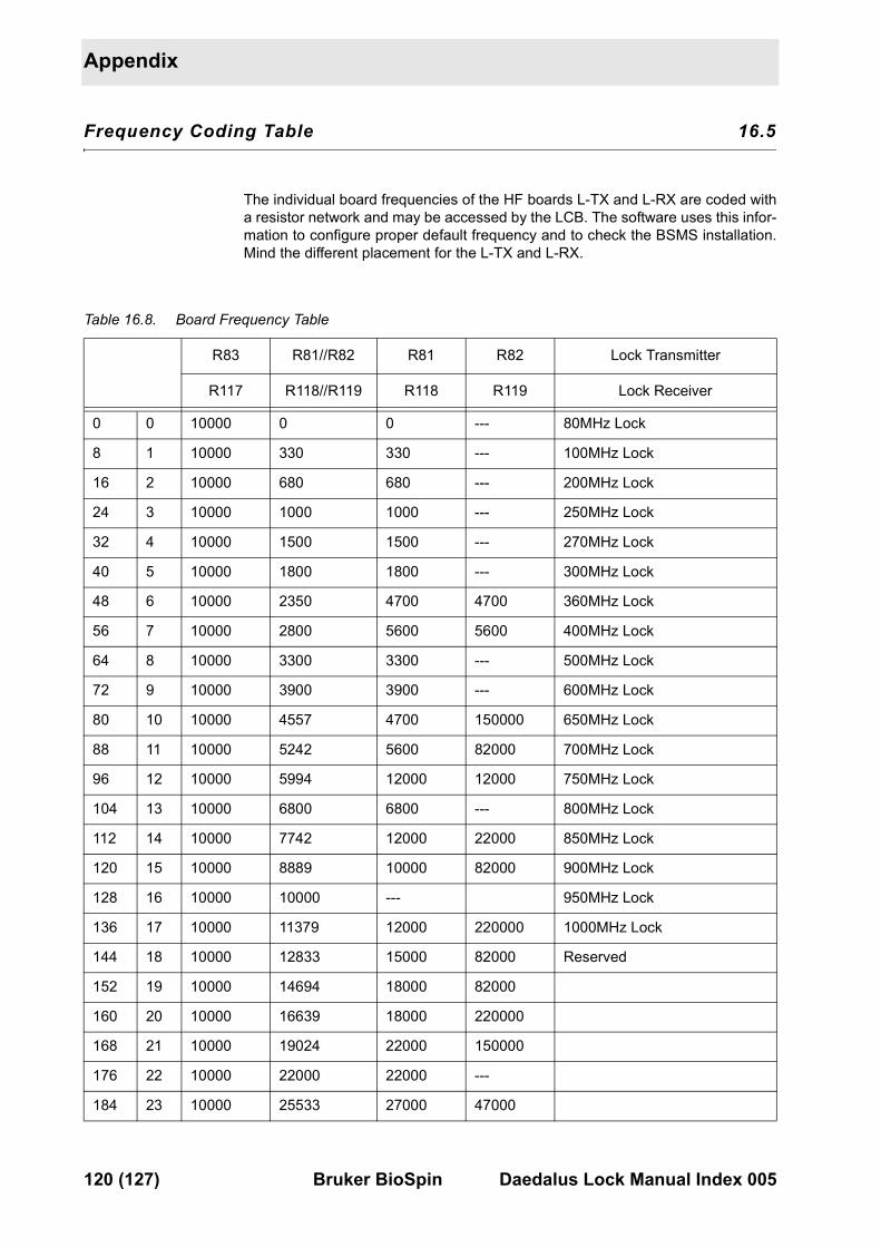
Appendix
Frequency Coding Table 16.5
0
The individual board frequencies of the HF boards L-TX and L-RX are coded with a resistor network and may be accessed by the LCB. The software uses this infor-mation to configure proper default frequency and to check the BSMS installation. Mind the different placement for the L-TX and L-RX.
Table 16.8. Board Frequency Table
R83 R81//R82 R81 R82 Lock Transmitter
R117 R118//R119 R118 R119 Lock Receiver
0 0 10000 0 0 --- 80MHz Lock
8 1 10000 330 330 --- 100MHz Lock
16 2 10000 680 680 --- 200MHz Lock
24 3 10000 1000 1000 --- 250MHz Lock
32 4 10000 1500 1500 --- 270MHz Lock
40 5 10000 1800 1800 --- 300MHz Lock
48 6 10000 2350 4700 4700 360MHz Lock
56 7 10000 2800 5600 5600 400MHz Lock
64 8 10000 3300 3300 --- 500MHz Lock
72 9 10000 3900 3900 --- 600MHz Lock
80 10 10000 4557 4700 150000 650MHz Lock
88 11 10000 5242 5600 82000 700MHz Lock
96 12 10000 5994 12000 12000 750MHz Lock
104 13 10000 6800 6800 --- 800MHz Lock
112 14 10000 7742 12000 22000 850MHz Lock
120 15 10000 8889 10000 82000 900MHz Lock
128 16 10000 10000 --- 950MHz Lock
136 17 10000 11379 12000 220000 1000MHz Lock
144 18 10000 12833 15000 82000 Reserved
152 19 10000 14694 18000 82000
160 20 10000 16639 18000 220000
168 21 10000 19024 22000 150000
176 22 10000 22000 22000 ---
184 23 10000 25533 27000 47000
120 (127) Bruker BioSpin Daedalus Lock Manual Index 005
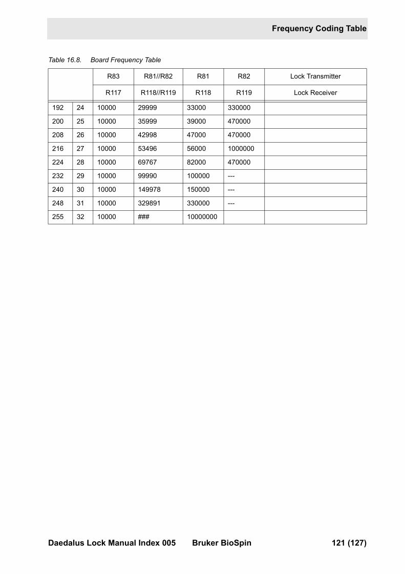
Frequency Coding Table
192 24 10000 29999 33000 330000
200 25 10000 35999 39000 470000
208 26 10000 42998 47000 470000
216 27 10000 53496 56000 1000000
224 28 10000 69767 82000 470000
232 29 10000 99990 100000 ---
240 30 10000 149978 150000 ---
248 31 10000 329891 330000 ---
255 32 10000 ### 10000000
Table 16.8. Board Frequency Table
R83 R81//R82 R81 R82 Lock Transmitter
R117 R118//R119 R118 R119 Lock Receiver
Daedalus Lock Manual Index 005 Bruker BioSpin 121 (127)
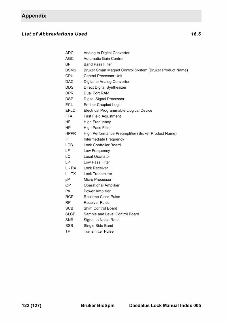
Appendix
List of Abbreviations Used 16.6
0
ADC Analog to Digital ConverterAGC Automatic Gain ControlBP Band Pass Filter BSMS Bruker Smart Magnet Control System (Bruker Product Name)CPU Central Processor UnitDAC Digital to Analog ConverterDDS Direct Digital SynthesizerDPR Dual Port RAMDSP Digital Signal ProcessorECL Emitter Coupled LogicEPLD Electrical Programmable Llogical DeviceFFA Fast Field AdjustmentHF High FrequencyHP High Pass Filter HPPR High Performance Preamplifier (Bruker Product Name)IF Intermediate FrequencyLCB Lock Controller BoardLF Low FrequencyLO Local OscillatorLP Low Pass FilterL - RX Lock ReceiverL - TX Lock Transmitter�P Micro ProcessorOP Operational AmplifierPA Power AmplifierRCP Realtime Clock PulseRP Receiver PulseSCB Shim Control BoardSLCB Sample and Level Control BoardSNR Signal to Noise RatioSSB Single Side BandTP Transmitter Pulse
122 (127) Bruker BioSpin Daedalus Lock Manual Index 005
Figures
Contents 3
Index 7
1 Introduction 15
2 General Description 17Figure 2.1. Lock Function Diagram ....................................................... 18Figure 2.2. Block Diagram of the Lock .................................................. 20
3 Operation 23Figure 3.1. Lock Keyboard Menu Tree ................................................. 31Figure 3.2. Lock-Hold Pulse Diagram for AV Spectrometers .................. 32
4 19F Lock Option 35Figure 4.1. L-TX Option 19F Installation ............................................... 37Figure 4.2. L-RX Option 19F Installation ............................................... 38Figure 4.3. 19F Wiring ......................................................................... 39
5 Lock Transmitter 43Figure 5.1. Transmitter Block Diagram ................................................. 43Figure 5.2. Front View L-TX ECL05 with pulse setting switch ................ 50Figure 5.3. Transmitter Blanking Sequence for ECL00 and ECL01 ........ 51Figure 5.4. Transmitter Blanking Sequence from ECL02 on .................. 51Figure 5.5. Pulse diagram for PFP (Normal Lock mode, T=300s) ........ 54Figure 5.6. Pulse diagram for PFP Mode ECL05 and higher (T=300s) 55Figure 5.7. Pulse diagram for FFA Mode .............................................. 57
6 19F TX Option 61Figure 6.1. 19F TX Option Block Diagram ............................................ 62
7 Lock Receiver 65Figure 7.1. Receiver Block Diagram ..................................................... 65Figure 7.2. Block Diagram of Receiver Concept ................................... 66
8 19F RX Option 69Figure 8.1. Signal path in Receiver with built in Option. ........................ 69Figure 8.2. X_Option Block Diagram .................................................... 70
9 Lock Controller 73
Daedalus Lock Manual Index 005 Bruker BioSpin 123 (127)
Figures
Figure 9.1. Controller Block Diagram ................................................... 73Figure 9.2. Lock Controller Memory Maps ............................................ 75Figure 9.3. Lock Controller Memory Maps (continued) .......................... 76Figure 9.4. Downloading the DSP Software (Timing diagram) ............... 78Figure 9.5. Serial Lock Control Bus Diagram ........................................ 80Figure 9.6. Serial Lock Control Bus Timing Diagram ............................ 81
10 Lock RS232 Piggy Board 85Figure 10.1. Connections with the Mainboard ........................................ 86
11 Hold Interface for AVANCE Spectrometers 87Figure 11.1. LCB board component mounting diagram ECL02 to ECL03 89Figure 11.2. LCB Board component mounting diagram ........................... 91Figure 11.3. LCB board component mounting diagram ........................... 91Figure 11.4. LCB Board component mounting after modification ............ 92
12 Technical Data 93
13 Trouble Shooting 97
14 BSMS service tool 99Figure 14.1. Mode Register (L-TX IC27) .............................................. 104
15 Lock Error Messages 107
16 Appendix 115
Figures 123
Tables 125
124 (127) Bruker BioSpin Daedalus Lock Manual Index 005
Tables
Contents 3
Index 7
1 Introduction 15
2 General Description 17Table 2.1. Unit numbers for different instrument frequencies .......... 21
3 Operation 23Table 3.1. Lock Parameters ............................................................ 27Table 3.2. Lock Parameters corresponding to the old analog Lock .. 28Table 3.3. Default values (factory configuration) ............................. 28
4 19F Lock Option 35Table 4.1. BSMS Unit numbers for different instrument frequencies 35
5 Lock Transmitter 43Table 5.1. Assisting Frequencies for various Instrument Versions ... 46Table 5.2. Pulsebanks (EPROMs) and Counters ............................. 56Table 5.3. PAL Outputs at the various operating modes .................. 58Table 5.4. L-TX Print Versions ........................................................ 59
6 19F TX Option 61
7 Lock Receiver 65Table 7.1. L-RX Print Version ......................................................... 68
8 19F RX Option 69Table 8.1. 19F-RX Option Print Version .......................................... 71
9 Lock Controller 73Table 9.1. SCI Interface Frame ...................................................... 79Table 9.2. LCB Print Version .......................................................... 83
10 Lock RS232 Piggy Board 85
11 Hold Interface for AVANCE Spectrometers 87
Daedalus Lock Manual Index 005 Bruker BioSpin 125 (127)
Tables
12 Technical Data 93
13 Trouble Shooting 97
14 BSMS service tool 99
15 Lock Error Messages 107Table 15.1. Lock Error Messages in alphabetical order .................. 107
16 Appendix 115Table 16.1. Technical Data for the H0 Coil ..................................... 115Table 16.2. H0 Frequency and Regulating Range .......................... 116Table 16.3. Deuterium Frequencie which correspond with the old Analog-
Lock 116Table 16.4. New Deuterium Frequencies ........................................ 117Table 16.5. Fluorine Frequency Generation ................................... 118Table 16.6. Some Representative 2H Chemical Shifts .................... 119Table 16.7. Some Representative 19F Chemical Shifts Referenced to
CFCl3 119Table 16.8. Board Frequency Table ................................................ 120
Figures 123
Tables 125
126 (127) Bruker BioSpin Daedalus Lock Manual Index 005

Notizen
Daedalus Lock Manual Index 005 Bruker BioSpin 127 (127)
Lastpage
Index
Numerics
19F Chemical Shifts .......................................................................................... 11919F RX Option ........................................................................................ 35, 61, 6919F TX Option..................................................................................................... 6119F_LO signal..................................................................................................... 3619F_LO-signa ..................................................................................................... 6219F-Operation ..................................................................................................... 4019F-Option Installation ........................................................................................ 3519F-Wiring........................................................................................................... 392H Chemical Shifts............................................................................................ 1192H-TR.................................................................................................................. 5160MHz Multiplier ................................................................................................. 4480535 microprocessor......................................................................................... 19
A
A/D converter ...................................................................................................... 68Absorption ........................................................................................................... 68Acetone-d6.......................................................................................................... 25Acquisition........................................................................................................... 68Acquisition-Parameters ....................................................................................... 40Active Bandpassfilter........................................................................................... 67ADC diagnostic ................................................................................................. 103AGC Amplifiers.................................................................................................... 47AMX .................................................................................................................... 87applications software......................................................................................... 107ARX..................................................................................................................... 87ASX..................................................................................................................... 87Attenuator............................................................................................................ 70Auto Gain ............................................................................................................ 23Auto Lock ............................................................................................................ 23Auto Phase.......................................................................................................... 23Auto Power.......................................................................................................... 23Autolock ...................................................................................................... 24, 104Autolock H0 Calibration..................................................................................... 104Autolock Mode .................................................................................................. 100AVANCE ............................................................................................................. 87AVANCE spectrometers...................................................................................... 34
B
Baudrate.............................................................................................................. 79beep (buzzer) ...................................................................................................... 30Blackman Window................................................................................... 17, 53, 94blanking............................................................................................................. 101Bloch ................................................................................................................... 17
Daedalus Lock Manual Index 005 Bruker BioSpin 7 (127)
Index
Boot EPROM..................................................................................................... 107BSMS Keyboard.................................................................................................. 23BSMS Servicetool ............................................................................................... 39Buffer Amplifier.................................................................................................... 70
C
Cables ................................................................................................................. 36Calibration ......................................................................................................... 104Caution Lock Frequency ........................................................................... 100, 103Chemical Shifts ........................................................................................... 40, 117compound ........................................................................................................... 40Config................................................................................................................ 100Configurable TP-F0 requires L_TX with ECL02 or newer................................. 107Controller Board .................................................................................................. 19controller DAC................................................................................................... 105controller out ..................................................................................................... 102Controller Pulses................................................................................................. 53Cryoprobes.......................................................................................................... 50Current Source.................................................................................................. 103current source ................................................................................................... 104
D
DC Decoupling .................................................................................................... 71DDS................................................................................................................... 102DDS (Direct Digital Synthesizer) Diagnostic ..................................................... 103DDS Frequency................................................................................................... 46DDS frequency.................................................................................................. 103DDSFreqBusError ............................................................................................. 107DDSPhaseBusError .......................................................................................... 107default 2H frequency ......................................................................................... 103default DDS frequency ...................................................................................... 103default values ...................................................................................................... 99Delete Error ......................................................................................................... 99Deuterium............................................................................................................ 17Deuterium Frequency.......................................................................... 46 – 47, 116Deuterium local oscillating signal ........................................................................ 44Deuterium transmitter signal ............................................................................... 44development and debug tools ........................................................................... 105Diagnostic ......................................................................................................... 103difference experiments........................................................................................ 26Digital Analog Converter (DAC) .......................................................................... 44Digital Lock Settings............................................................................................ 19Digital Synthesizer .............................................................................................. 19Direct Digital Synthesizer (DDS) ................................................................... 44, 46Dispersion ........................................................................................................... 68Display ................................................................................................................ 24Display Data........................................................................................................ 78Display jumpers................................................................................................... 82Display Mode ................................................................................................ 24, 32Display mode .................................................................................................... 101dividers................................................................................................................ 62DownLoad ........................................................................................................... 99DP_RAMError ................................................................................................... 107
8 (127) Bruker BioSpin Daedalus Lock Manual Index 005
Index
Drift...................................................................................................................... 17Drift Comp........................................................................................................... 24DSP............................................................................................................. 77 – 78DSP Command not accepted............................................................................ 108DSP Host Interface ............................................................................................. 77DSP RAM Checksum........................................................................................ 108DSPDownLoadError.......................................................................................... 108DSPNoSerialData ............................................................................................. 108
E
ECL ................................................................................................... 59, 68, 71, 83ECL02 ................................................................................................................. 52ECL03 ................................................................................................................. 89ECL04 ..................................................................................................... 33, 88, 90EraseFail ........................................................................................................... 108Erasing Flash EPROM........................................................................................ 99Error 0 ............................................................................................................... 110Error 10 ............................................................................................................. 112Error 11 ............................................................................................................. 107Error 12 ............................................................................................................. 107Error 13 ............................................................................................................. 112Error 130 ........................................................................................................... 109Error 131 ........................................................................................................... 112Error 132 ........................................................................................................... 107Error 133 ........................................................................................................... 107Error 134 ........................................................................................................... 109Error 135 ........................................................................................................... 108Error 143 ........................................................................................................... 109Error 144 ........................................................................................................... 110Error 146 ........................................................................................................... 108Error 148 ........................................................................................................... 108Error 149 ........................................................................................................... 110Error 150 ........................................................................................................... 110Error 151 ........................................................................................................... 111Error 152 ........................................................................................................... 111Error 153 ........................................................................................................... 113Error 155 ........................................................................................................... 111Error 156 ........................................................................................................... 110Error 157 ........................................................................................................... 109Error 158 ........................................................................................................... 112Error 160 ........................................................................................................... 113Error 161 ........................................................................................................... 113Error 162 ........................................................................................................... 110Error 163 ........................................................................................................... 112Error 167 ........................................................................................................... 108Error 168 ........................................................................................................... 109Error 169 ........................................................................................................... 107Error 22 ............................................................................................................. 112Error 30 ............................................................................................................. 109Error 4 ............................................................................................................... 108Error 51 ............................................................................................................. 109Error 53 ............................................................................................................. 110Error 8 ............................................................................................................... 113Error Code......................................................................................................... 108
Daedalus Lock Manual Index 005 Bruker BioSpin 9 (127)
Index
Error Code = 12................................................................................................. 114Error Code = 31................................................................................................. 113Error Code = 32................................................................................................. 113Error Code = 33................................................................................................. 114Error Code = 34................................................................................................. 114Error Code = 36................................................................................................. 112Error Code = 39................................................................................................. 111Error Code 38.................................................................................................... 114Error Messages................................................................................................. 107Error_Startchar.................................................................................................. 109ErrorOnLCB ...................................................................................................... 108
F
FFA Amplifier Diagnostic................................................................................... 103FFA Mode ..................................................................................................... 44, 48FFA Spectrum ................................................................................................... 102FFAError ........................................................................................................... 109FFA-Spectrum..................................................................................................... 24FIELD .................................................................................................................. 23Field .................................................................................................................... 24figure of merit ...................................................................................................... 27Fluorine ............................................................................................................... 61Fluorine (as lock substance) ............................................................................... 17Fluorine-Lock-Option........................................................................................... 35Function due to Lock actions temjporary disabled ............................................ 109
G
GainBusError .................................................................................................... 109Galvanic Isolation................................................................................................ 18gradients ............................................................................................................. 32Graphic Terminal................................................................................................. 78GT01 ............................................................................................................. 78, 82
H
H0 Power Source ................................................................................................ 19H0_CURRENT .................................................................................................. 105Hardware) Version .............................................................................................. 83HF Amplifier ........................................................................................................ 67HF Bandpass Filter ............................................................................................. 67HF Parameters.................................................................................................... 79HF Power Supply Failure .................................................................................. 109Highpass Filter .................................................................................................... 70hold off ................................................................................................................ 33hold on ................................................................................................................ 33Hold Operation .................................................................................................... 32Hold Pulse Polarity ...................................................................................... 88, 101HPPR .................................................................................................................. 52HPPR 19F-Selective module .............................................................................. 35HPPR Gating Pulse TP-F0.................................................................................. 52HWTest Functions not supported...................................................................... 109HWTesterIsOn .................................................................................................. 109
10 (127) Bruker BioSpin Daedalus Lock Manual Index 005
Index
I
ii........................................................................................................................... 40imaginary part ................................................................................................... 101Init ....................................................................................................................... 99
J
Jumper ................................................................................................................ 78Jumper Setting .............................................................................................. 79, 82
K
Keyboard............................................................................................................. 31
L
L_HOLD pulse..................................................................................................... 88L_SUBST .......................................................................................................... 104LF-Amplifier......................................................................................................... 67Lock Channel ...................................................................................................... 17Lock Controller LCB............................................................................................ 21Lock DC .............................................................................................................. 23Lock Drift ............................................................................................................. 23Lock Gain ............................................................................................................ 19Lock Hold Pulse Polarity ................................................................................... 101Lock in Spike....................................................................................................... 32Lock Parameters ................................................................................................. 23Lock Phase ......................................................................................................... 23Lock Power ......................................................................................................... 23Lock RF Gain ...................................................................................................... 23Lock Setting ........................................................................................................ 31Lock Settings for 19F .......................................................................................... 41Lock Shift .............................................................................................. 17, 23, 102Lock Substance................................................................................................... 40Lock-Hold Trouble shooting ................................................................................ 33Lock-In ................................................................................................................ 25Lockin PStep....................................................................................................... 24Locklost ............................................................................................................. 105Lock-Shift ............................................................................................................ 40LOOP FILTER..................................................................................................... 24Loop Gain............................................................................................................ 24Loop Time ........................................................................................................... 24Lowpass Filter ..................................................................................................... 71
M
Magnet Type ..................................................................................................... 100Manual Lock In.................................................................................................... 31Manual Lock-In.................................................................................................... 25Menu Tree........................................................................................................... 31Mixer ................................................................................................................... 70Mode Register................................................................................................... 104
Daedalus Lock Manual Index 005 Bruker BioSpin 11 (127)
Index
ModeBusError ................................................................................................... 109MX..................................................................................................................... 102MY..................................................................................................................... 102
N
NMR Control Word.............................................................................................. 32No Communication with DSP............................................................................ 110No FFA Amplifier Signal .................................................................................... 110No FFASignal Found......................................................................................... 110No H0 Coilcurrent.............................................................................................. 110No Option .......................................................................................................... 110No Quadmixer Signal ........................................................................................ 111No RFOut Signal ............................................................................................... 111No T2H DDSSignal ........................................................................................... 111noise modulation ................................................................................................. 27normal lock mode.............................................................................................. 104NotSameBootRoutine ....................................................................................... 111
O
Operation ............................................................................................................ 23Option (19F) ............................................................................................ 70, 93, 95Options.............................................................................................................. 105
P
P_BNK0..P_BNK3............................................................................................. 104PFP Mode ..................................................................................................... 44, 48phase detector .................................................................................................... 62phase locked oscillator........................................................................................ 62PI Regulator ........................................................................................................ 24PLL.............................................................................................................. 62, 105PLL ERROR...................................................................................................... 112power .................................................................................................................. 99Power Bus Error................................................................................................ 112Power Supply Diagnostic .................................................................................. 103PowerFail .......................................................................................................... 112ppm ..................................................................................................................... 40Print Number ..................................................................................... 59, 68, 71, 83ProgrammerFail ................................................................................................ 112Pulsbanks.......................................................................................................... 104Pulse Bank .......................................................................................................... 49Pulse Program .................................................................................................... 33Pulse Section ................................................................................................ 19, 49Pulses ............................................................................................................... 104
Q
QuadMixer Diagnostic....................................................................................... 103Quadrature Mixer .......................................................................................... 44, 47
12 (127) Bruker BioSpin Daedalus Lock Manual Index 005
Index
R
RAM Error ......................................................................................................... 112RCP Interface...................................................................................................... 76Read Lock Level ............................................................................................... 102real part ............................................................................................................. 101real part expanded ............................................................................................ 102real part low pass filtered .................................................................................. 101Rec. Blanking .................................................................................................... 101Rec. Blanking On/Off ........................................................................................ 101Receiver ............................................................................................ 19, 35, 69, 93Receiver AGC Voltage Diagnostic .................................................................... 103Receiver Blanking ............................................................................................... 53receiver gain overflow ......................................................................................... 26Reference Signal................................................................................................. 44Regulator Gain .................................................................................................... 24Regulator Output................................................................................................. 24regulator output ................................................................................................... 32Regulator Time Constant .................................................................................... 24reset .................................................................................................................... 99Reset and Power up Logic .................................................................................. 76RP1 ................................................................................................................... 104RS Baudrate........................................................................................................ 79RS232 ......................................................................................................... 78 – 79RS232 Piggy Board............................................................................................. 85RS-Baudrate ....................................................................................................... 24RX AGC Voltage Failure ................................................................................... 112RX_BLNK............................................................................................................ 49RX_BLNK ON ................................................................................................... 104RxOpt TxOpt .................................................................................................... 113RX-pulse delay.................................................................................................... 50RxTyp TxTyp.................................................................................................... 113
S
saturation .................................................................................................... 25 – 26Save Config....................................................................................................... 103Save Lock Settings ........................................................................................... 104SCI Interface ....................................................................................................... 79SCI jumpers ........................................................................................................ 82service tool .......................................................................................................... 99Shift ..................................................................................................................... 24SHIFT/FIELD....................................................................................................... 24Shift/Field .......................................................................................................... 100sidebands............................................................................................................ 25Signal Processor ................................................................................................. 19software............................................................................................................... 99softwarehandshake............................................................................................. 79SSI Interface ....................................................................................................... 78standard bore .................................................................................................... 100standard field..................................................................................................... 102STD BY ............................................................................................................... 99Substance ......................................................................................................... 100super wide bore................................................................................................. 100Sweep ................................................................................................................. 23
Daedalus Lock Manual Index 005 Bruker BioSpin 13 (127)
Index
Sweep Amplitude ................................................................................................ 23Sweep Rate......................................................................................................... 23sweep wiggles..................................................................................................... 25Syntax Error ...................................................................................................... 113
T
Too much Noise on ADC .................................................................................. 113TP...................................................................................................................... 104TP_F0 ................................................................................................................. 51TP-F0 .................................................................................................................. 52Trans Blanking .................................................................................................. 101Trans Blanking On/Off....................................................................................... 101Transmitter ........................................................................................ 19, 35, 69, 94Transmitter Blank Mod ........................................................................................ 49Transmitter Blanking ..................................................................................... 51, 53Transmitter HFSection Diagnostic .................................................................... 103Transmitter Power Range ................................................................................... 48Transmitter Subsections ..................................................................................... 44TX_BL ................................................................................................................. 51TX_BLNK ............................................................................................................ 49TX_BLNK Off .................................................................................................... 104
U
Upgrade from LCB ECL02 to ECL03 .................................................................. 89Upgrade from LCB ECL03 to ECL04 .................................................................. 90Upgrade to ECL01 .............................................................................................. 85UXNMR ............................................................................................................... 40
V
Variable Lock Parameters................................................................................... 23Version .............................................................................................................. 100VME Interface ......................................................................................... 19, 74, 76
W
wide bore........................................................................................................... 100wiggles ................................................................................................................ 25Wrong AppSW .................................................................................................. 114Wrong Datacount .............................................................................................. 113Wrongaddress................................................................................................... 113WrongCheckSum .............................................................................................. 114WrongRecord Type ........................................................................................... 114WrongTransmissionCheck ................................................................................ 114
X
X32 Commands .................................................................................................. 19XOFF................................................................................................................... 79XON .................................................................................................................... 79
14 (127) Bruker BioSpin Daedalus Lock Manual Index 005
Introduction 11000000
About DaedalusThose of you with a knowledge of ancient Greek history will no doubt recognise the name we have used for our new digital lock. Daedalus and his son Icarus, in an effort to flee from one island to another, built two sets of wings in order to fly to freedom. The wings were constructed of feathers glued to a wicker frame with wax. The wings functioned beautifully and they set over the ocean. In his joy Icarus flew higher and higher and, heeding Daedalus no longer, plunged to his death after flying too close to the Sun. His wax had melted and the wings disinte-grated. His wise father Daedalus flew on for a great distance - safely reaching his goal.
Just as the original Daedalus came to be a legend so too is our Digital Daedalus Lock System destined to receive great acclaim. Inspired by the same soaring phi-losophy and thorough preparation our Daedalus Lock will perform for you to achieve the ever more exacting demands for NMR in the 90’s!
Your Manual ContainsYour manual features three major areas to help you quickly locate your subject of interest.
The first two chapters -‘General Description’ and ‘Operation’ - provide an overview of the entire system with specifics for operation.
The following three chapters ‘Lock Transmitter’, ‘Lock Receiver’, and ‘Lock Con-troller’ cover in detail the print boards from which the Digital Lock is constructed. Function descriptions, general information, schematics, diagrams and testing in-formation for the boards are all located in this mid section.
The final chapters give you an overview of the System Software, Technical Data, Error Messages and Correcting Technique. The appendix includes various fre-quency and range information and a list of abbreviations we hope you will find useful.
For your convenience we have also included at the rear a ‘List of Figures’ and a ‘List of Tables’.
Sincerely Yours
‘The Daedalus Team’
Daedalus Lock Manual Index 005 Bruker BioSpin 15 (127)

Introduction
16 (127) Bruker BioSpin Daedalus Lock Manual Index 005