Embed Size (px)
Citation preview
BSIM4.5.0 MOSFET Model
- User’s Manual
Xuemei (Jane) Xi, Mohan Dunga, Jin He, Weidong Liu, Kanyu M. Cao, Xiaodong Jin, Jeff J. Ou, Mansun Chan, Ali M. Niknejad,
Chenming Hu
Department of Electrical Engineering and Computer Sciences
University of California, Berkeley, CA 94720
Copyright © 2004The Regents of the University of California
All Rights Reserved
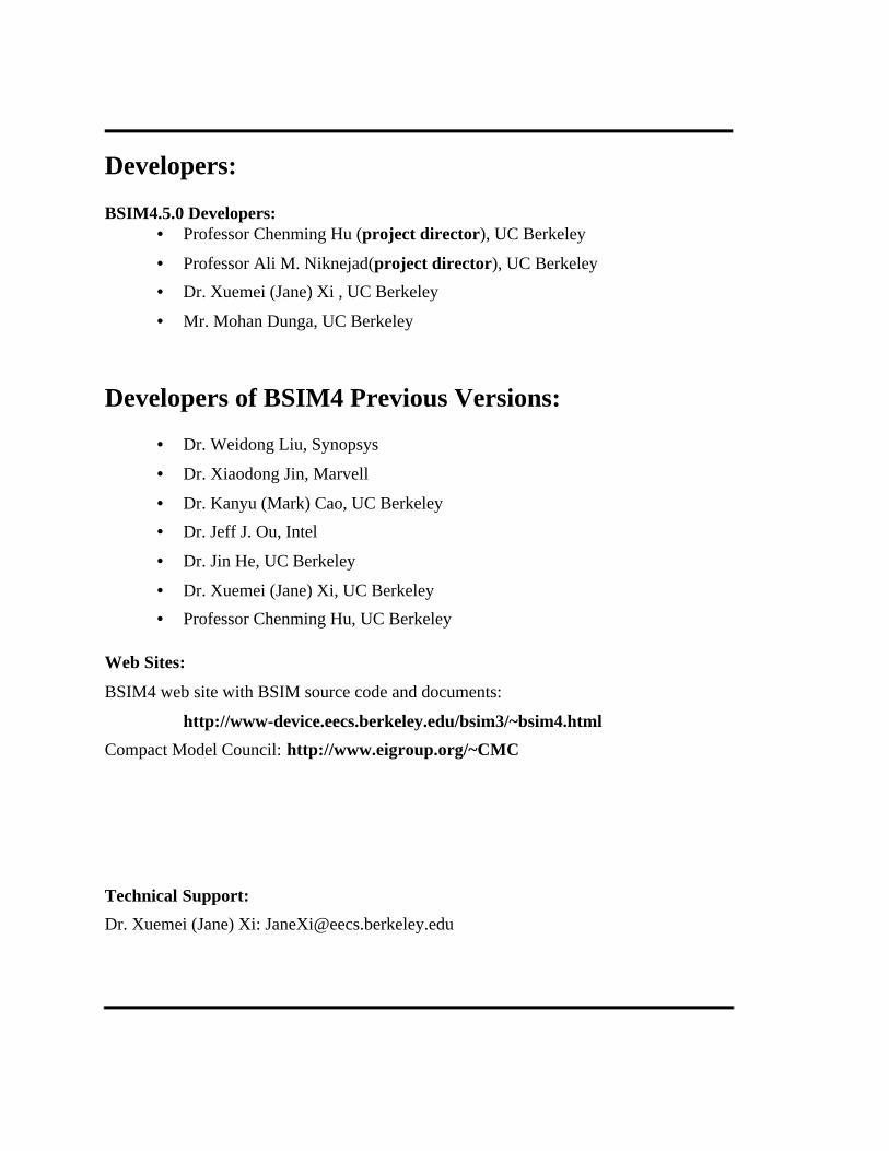
Developers:
BSIM4.5.0 Developers:• Professor Chenming Hu (project director), UC Berkeley
• Professor Ali M. Niknejad(project director), UC Berkeley
• Dr. Xuemei (Jane) Xi , UC Berkeley
• Mr. Mohan Dunga, UC Berkeley
Developers of BSIM4 Previous Versions:
• Dr. Weidong Liu, Synopsys
• Dr. Xiaodong Jin, Marvell
• Dr. Kanyu (Mark) Cao, UC Berkeley
• Dr. Jeff J. Ou, Intel
• Dr. Jin He, UC Berkeley
• Dr. Xuemei (Jane) Xi, UC Berkeley
• Professor Chenming Hu, UC Berkeley
Web Sites:
BSIM4 web site with BSIM source code and documents:
http://www-device.eecs.berkeley.edu/bsim3/~bsim4.html
Compact Model Council: http://www.eigroup.org/~CMC
Technical Support:
Dr. Xuemei (Jane) Xi: [email protected]
Acknowledgement:
The development of BSIM4.5.0 benefited from the input of many BSIM
users, especially the Compact Model Council (CMC) member companies.
The developers would like to thank Keith Green, Tom Vrotsos, Suhail
Murtaza, David Zweidinger, Britt Brooks and Doug Weiser at TI, Joe
Watts and Richard Q Williams at IBM, Yu-Tai Chia, Ke-Wei Su, Chung-
Kai Chung, and Y-M Sheu at TSMC, Rainer Thoma, Ivan To, Young-Bog
Park and Colin McAndrew at Motorola, Paul Humphries, Geoffrey J.
Coram and Andre Martinez at Analog Devices, Andre Juge and Gilles
Gouget at STmicroelectronics, Mishel Matloubian at Mindspeed, Judy An
at AMD, Bernd Lemaitre, Joachim Assenmacher, Laurens Weiss and Peter
Klein at Infinion, Ping-Chin Yeh and Dick Dowell at HP, Shiuh-Wuu Lee,
Wei-Kai Shih, Paul Packan, Sivakumar P Mudanai and Rafael Rio at Intel,
Xiaodong Jin at Marvell, Weidong Liu at Synopsys, Marek Mierzwinski at
Tiburon-DA, Jean-Paul MALZAC at Silvaco, Min-Chie Jeng, Ping Chen,
Jushan Xie, and Zhihong Liu at Cadence, Mohamed Selim and Ahmed
Ramadan at Mentor Graphics, Peter Lee, Kazunori Onozawa at Renesas,
Toshiyuki Saito and Shigetaka Kumashiro at NEC, Richard Taylor at NSC,
for their valuable assistance in identifying the desirable modifications and
testing of the new model.
The BSIM project is partially supported by SRC, and CMC.

BSIM4.5.0 Manual Copyright © 2005 UC Berkeley 1
Table of Contents
Chapter 1: Effective Oxide Thickness, Channel Length and Channel Width 1-1
1.1 Gate Dielectric Model 1-1
1.2 Poly-Silicon Gate Depletion 1-2
1.3 Effective Channel Length and Width 1-5
Chapter 2: Threshold Voltage Model 2-12.1 Long-Channel Model With Uniform Doping 2-1
2.2 Non-Uniform Vertical Doping 2-2
2.3 Non-Uniform Lateral Doping: Pocket (Halo) Implant 2-5
2.4 Short-Channel and DIBL Effects 2-6
2.5 Narrow-Width Effect 2-9
Chapter 3: Channel Charge and Subthreshold Swing Models 3-13.1 Channel Charge Model 3-1
3.2 Subthreshold Swing n 3-5
Chapter 4: Gate Direct Tunneling Current Model 4-14.1 Model selectors 4-2
4.2 Voltage Across Oxide Vox 4-2
4.3 Equations for Tunneling Currents 4-3
Chapter 5: Drain Current Model 5-15.1 Bulk Charge Effect 5-1
5.2Unified Mobility Model 5-2
5.3Asymmetric and Bias-Dependent Source/Drain Resistance Model 5-4
5.4 Drain Current for Triode Region 5-5
5.5 Velocity Saturation 5-7
5.6Saturation Voltage Vdsat 5-8
5.7Saturation-Region Output Conductance Model 5-10
5.8Single-Equation Channel Current Model 5-16
BSIM4.5.0 Manual Copyright © 2005 UC Berkeley 2
5.9 New Current Saturation Mechanisms: Velocity Overshoot and Source End Velocity Limit Model 5-17
Chapter 6: Body Current Models 6-16.1 Iii Model 6-1
6.2 IGIDL Model 6-2
Chapter 7: Capacitance Model 7-17.1 General Description 7-1
7.2Methodology for Intrinsic Capacitance Modeling 7-3
7.3Charge-Thickness Capacitance Model (CTM) 7-9
7.4Intrinsic Capacitance Model Equations 7-13
7.5Fringing/Overlap Capacitance Models 7-19
Chapter 8: High-Speed/RF Modelsm 8-18.1Charge-Deficit Non-Quasi-Static (NQS) Model 8-1
8.2Gate Electrode Electrode and Intrinsic-Input Resistance (IIR) Model 8-6
8.3Substrate Resistance Network 8-8
Chapter 9: Noise Modeling 9-19.1 Flicker Noise Models 9-1
9.2Channel Thermal Noise 9-4
9.3Other Noise Sources Modeled 9-7
Chapter 10: Asymmetric MOS Junction Diode Models 10-110.1Junction Diode IV Model 10-1
10.2Junction Diode CV Model 10-6
Chapter 11: Layout-Dependent Parasitics Model 11-111.1 Geometry Definition 11-1
11.2Model Formulation and Options 11-3
Chapter 12: Temperature Dependence Model 12-112.1Temperature Dependence of Threshold Voltage 12-1
BSIM4.5.0 Manual Copyright © 2005 UC Berkeley 3
12.2Temperature Dependence of Mobility 12-1
12.3Temperature Dependence of Saturation Velocity 12-2
12.4Temperature Dependence of LDD Resistance 12-2
12.5Temperature Dependence of Junction Diode IV 12-3
12.6Temperature Dependence of Junction Diode CV 12-5
12.7Temperature Dependences of Eg and ni 12-8
Chapter 13: Stress Effect Model 13-113.1 Stress effect model development 13-1
13.2 Effective SA and SB for irregular LOD 13-2
Chapter 14: Well Proximity Effect Model 14-114.1 Well Proximity effect model development 14-1
14.2 Extraction of Instance Parameters (for post-layout simulation) 14-2
Chapter 15: Parameter Extraction Methodology 15-115.1Optimization strategy 15-1
15.2 Extraction Strategy 15-2
15.3Extraction Procedure 15-3
Appendix A: Complete Parameter List A-1A.1BSIM4.0.0 Model Selectors/Controllers A-1
A.2 Process Parameters A-3
A.3Basic Model Parameters A-5
A.4Parameters for Asymmetric and Bias-Dependent Rds Model A-10
A.5Impact Ionization Current Model Parameters A-11
A.6Gate-Induced Drain Leakage Model Parameters A-11
A.7Gate Dielectric Tunneling Current Model Parameters A-12
A.8Charge and Capacitance Model Parameters A-15
A.9High-Speed/RF Model Parameters A-17
A.10Flicker and Thermal Noise Model Parameters A-18
A.11Layout-Dependent Parasitics Model Parameters A-19
A.12Asymmetric Source/Drain Junction Diode Model Parameters A-20
A.13Temperature Dependence Parameters A-23
BSIM4.5.0 Manual Copyright © 2005 UC Berkeley 4
A.14dW and dL Parameters A-25
A.15Range Parameters for Model Application A-26
A.16 Notes 1-8 A-26
Appendix B: Core Parameter List for General Parameter Extraction B-1
Appendix C: References C-1‘
BSIM4.5.0 Manual Copyright © 2005 UC Berkeley 1-1
Chapter 1: Effective Oxide Thickness, Channel Length and Channel Width
BSIM4, as the extension of BSIM3 model, addresses the MOSFET physical
effects into sub-100nm regime. The continuous scaling of minimum feature size
brought challenges to compact modeling in two ways: One is that to push the
barriers in making transistors with shorter gate length, advanced process
technologies are used such as non-uniform substrate doping. The second is its
opportunities to RF applications.
To meet these challenges, BSIM4 has the following major improvements and
additions over BSIM3v3: (1) an accurate new model of the intrinsic input
resistance for both RF, high-frequency analog and high-speed digital applications;
(2) flexible substrate resistance network for RF modeling; (3) a new accurate
channel thermal noise model and a noise partition model for the induced gate
noise; (4) a non-quasi-static (NQS) model that is consistent with the Rg-based RF
model and a consistent AC model that accounts for the NQS effect in both
transconductances and capacitances. (5) an accurate gate direct tunneling model
for multiple layer gate dielectrics; (6) a comprehensive and versatile geometry-
dependent parasitics model for various source/drain connections and multi-finger
devices; (7) improved model for steep vertical retrograde doping profiles; (8)
better model for pocket-implanted devices in Vth, bulk charge effect model, and
Rout; (9) asymmetrical and bias-dependent source/drain resistance, either internal
or external to the intrinsic MOSFET at the user's discretion; (10) acceptance of
either the electrical or physical gate oxide thickness as the model input at the user's
Gate Dielectric Model
1-2 BSIM4.5.0 Manual Copyright © 2005 UC Berkeley
choice in a physically accurate maner; (11) the quantum mechanical charge-layer-
thickness model for both IV and CV; (12) a more accurate mobility model for
predictive modeling; (13) a gate-induced drain/source leakage (GIDL/GISL)
current model, available in BSIM for the first time; (14) an improved unified
flicker (1/f) noise model, which is smooth over all bias regions and considers the
bulk charge effect; (15) different diode IV and CV charatistics for source and drain
junctions; (16) junction diode breakdown with or without current limiting; (17)
dielectric constant of the gate dielectric as a model parameter; (18) A new scalable
stress effect model for process induced stress effect; device performance
becoming thus a function of the active area geometry and the location of the
device in the active area; (19) A unified current-saturation model that includes all
mechanisms of current saturation- velocity saturation, velocity overshoot and
source end velocity limit; (20) A new temperature model format that allows
convenient prediction of temperature effects on saturation velocity, mobility, and
S/D resistances.
1.1Gate Dielectric Model
As the gate oxide thickness is vigorously scaled down, the finite charge-layer
thickness can not be ignored [1]. BSIM4 models this effect in both IV and CV. For
this purpose, BSM4 accepts two of the following three as the model inputs: the
electrical gate oxide thickness TOXE1, the physical gate oxide thickness TOXP,
and their difference DTOX = TOXE - TOXP. Based on these parameters, the effect
of effective gate oxide capacitance Coxeff on IV and CV is modeled [2].
1. Capital and italic alphanumericals in this manual are model parameters.
Gate Dielectric Model
BSIM4.5.0 Manual Copyright © 2005 UC Berkeley 1-3
High-k gate dielectric can be modeled as SiO2 (relative permittivity: 3.9) with an
equivalent SiO2 thickness. For example, 3nm gate dielectric with a dielectric
constant of 7.8 would have an equivalent oxide thickness of 1.5nm.
BSIM4 also allows the user to specify a gate dielectric constant (EPSROX)
different from 3.9 (SiO2) as an alternative approach to modeling high-k dielectrics.
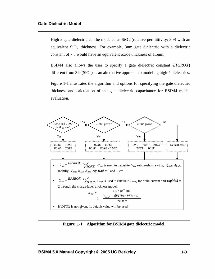
Figure 1-1 illustrates the algorithm and options for specifying the gate dielectric
thickness and calculation of the gate dielectric capacitance for BSIM4 model
evaluation.
Figure 1-1. Algorithm for BSIM4 gate dielectric model.
TOXE given?TOXE and TOXPboth given?
No
Yes
TOXP given?No
YesYes
No
TOXE ⇐ TOXETOXP ⇐ TOXP
TOXE ⇐ TOXETOXP ⇐ TOXE - DTOX
TOXE ⇐ TOXP + DTOXTOXP ⇐ TOXP
Default case
• TOXEEPSROXCoxe
0ε⋅= , Coxe is used to calculate Vth, subthreshold swing, Vgsteff, Abulk,
mobiliy, Vdsat, K1ox, K2ox, capMod = 0 and 1, etc
• TOXPEPSROXCoxp
0ε⋅= , Coxp is used to calculate Coxeff for drain current and capMod =
2 through the charge-layer thickness model:
( ) 7.0
9
2
041
cm109.1
Φ−−++
×=
−
TOXP
VFBVTHVX
sgsteff
DC
• If DTOX is not given, its default value will be used.
Poly-Silicon Gate Depletion
BSIM4.5.0 Manual Copyright © 2005 UC Berkeley 1-4
1.2 Poly-Silicon Gate Depletion
When a gate voltage is applied to the poly-silicon gate, e.g. NMOS with n+ poly-
silicon gate, a thin depletion layer will be formed at the interface between the poly-
silicon and the gate oxide. Although this depletion layer is very thin due to the high
doping concentration of the poly-silicon gate, its effect cannot be ignored since the
gate oxide thickness is small.
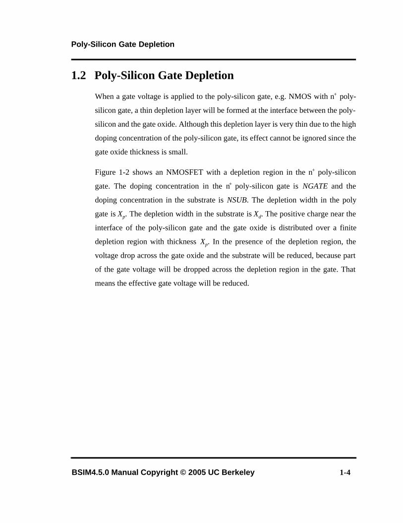
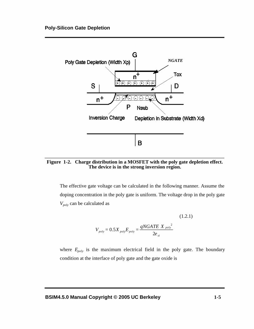
Figure 1-2 shows an NMOSFET with a depletion region in the n+ poly-silicon
gate. The doping concentration in the n+ poly-silicon gate is NGATE and the
doping concentration in the substrate is NSUB. The depletion width in the poly
gate is Xp. The depletion width in the substrate is Xd. The positive charge near the
interface of the poly-silicon gate and the gate oxide is distributed over a finite
depletion region with thickness Xp. In the presence of the depletion region, the
voltage drop across the gate oxide and the substrate will be reduced, because part
of the gate voltage will be dropped across the depletion region in the gate. That
means the effective gate voltage will be reduced.
Poly-Silicon Gate Depletion
BSIM4.5.0 Manual Copyright © 2005 UC Berkeley 1-5
Figure 1-2. Charge distribution in a MOSFET with the poly gate depletion effect. The device is in the strong inversion region.
The effective gate voltage can be calculated in the following manner. Assume the
doping concentration in the poly gate is uniform. The voltage drop in the poly gate
Vpoly can be calculated as
(1.2.1)
where Epoly is the maximum electrical field in the poly gate. The boundary
condition at the interface of poly gate and the gate oxide is
NGATE
si
polypolypolypoly
XqNGATEEXV
ε25.0
2⋅==

Poly-Silicon Gate Depletion
BSIM4.5.0 Manual Copyright © 2005 UC Berkeley 1-6
(1.2.2)
where Eox is the electric field in the gate oxide. The gate voltage satisfies
(1.2.3)
where Vox is the voltage drop across the gate oxide and satisfies Vox = EoxTOXE.
From (1.2.1) and (1.2.2), we can obtain
(1.2.4)
where
(1.2.5)
By solving (1.2.4), we get the effective gate voltage Vgse which is equal to
(1.2.6)
polysipolysiox VNGATEqEEEPSROX ⋅==⋅ εε 2
oxpolysFBgs VVVV +=Φ−−
( ) 02 =−−Φ−− polypolysFBgs VVVVa
2
2
2 TOXENGATEqEPSROX
asi ⋅
=ε
( )
−
⋅Φ−−
+⋅
+Φ+= 12
1 2
2
2
2
TOXENGATEqVFBVEPSROX
EPSROXTOXENGATEq
VFBVsi
sgssisgse ε
ε
Effective Channel Length and Width
BSIM4.5.0 Manual Copyright © 2005 UC Berkeley 1-7
1.3 Effective Channel Length and Width
The effective channel length and width used in the drain current model are given
below where XL and XW are parameters to account the channel length/width
offset due to mask/etch effect
(1.3.1)
(1.3.2a)
(1.3.2b)
The difference between (1.3.2a) and (1.3.2b) is that the former includes bias
dependencies. NF is the number of device fingers. dW and dL are modeled by
(1.3.3)
(1.3.4)
dLXLLL drawneff 2−+=
dWXWNF
WW drawn
eff 2−+=
'2' dWXWNF
WW drawn
eff −+=
( )
WWNWLNWWNWLN
sbseffsgsteff
WLWWL
WWW
LWL
WINTdW
VDWBVDWGdWdW
+++=
Φ−−Φ+⋅+=
'
'
LWNLLNLWNLLN WLLWL
WLW
LLL
LINTdL +++= LWNLLNLWNLLN WLLWL
WLW
LLL
LINTdL +++=
Effective Channel Length and Width
BSIM4.5.0 Manual Copyright © 2005 UC Berkeley 1-8
WINT represents the traditional manner from which "delta W" is extracted (from
the intercept of straight lines on a 1/Rds~Wdrawn plot). The parameters DWG and
DWB are used to account for the contribution of both gate and substrate bias
effects. For dL, LINT represents the traditional manner from which "delta L" is
extracted from the intercept of lines on a Rds~Ldrawn plot).
The remaining terms in dW and dL are provided for the convenience of the user.
They are meant to allow the user to model each parameter as a function of Wdrawn ,
Ldrawn and their product term. By default, the above geometrical dependencies for
dW and dL are turned off.
MOSFET capacitances can be divided into intrinsic and extrinsic components. The
intrinsic capacitance is associated with the region between the metallurgical source
and drain junction, which is defined by the effective length (Lactive) and width
(Wactive) when the gate to source/drain regions are under flat-band condition. Lactive
and Wactive are defined as
(1.3.5)
(1.3.6)
(1.3.7)
dLXLLL drawnactive 2−+=
dWXWNF
WW drawn
active 2−+=
LWNLLNLWNLLN WLLWLC
WLWC
LLLC
DLCdL +++=
Effective Channel Length and Width
BSIM4.5.0 Manual Copyright © 2005 UC Berkeley 1-9
(1.3.8)
The meanings of DWC and DLC are different from those of WINT and LINT in the
I-V model. Unlike the case of I-V, we assume that these dimensions are bias-
dependent. The parameter δLeff is equal to the source/drain to gate overlap length
plus the difference between drawn and actual POLY CD due to processing (gate
patterning, etching and oxidation) on one side.
The effective channel length Leff for the I-V model does not necessarily carry a
physical meaning. It is just a parameter used in the I-V formulation. This Leff is
therefore very sensitive to the I-V equations and also to the conduction
characteristics of the LDD region relative to the channel region. A device with a
large Leff and a small parasitic resistance can have a similar current drive as
another with a smaller Leff but larger Rds.
The Lactive parameter extracted from capacitance is a closer representation of the
metallurgical junction length (physical length). Due to the graded source/drain
junction profile, the source to drain length can have a very strong bias dependence.
We therefore define Lactive to be that measured at flat-band voltage between gate to
source/drain. If DWC, DLC and the length/width dependence parameters (LLC,
LWC, LWLC, WLC, WWC and WWLC) are not specified in technology files,
BSIM4 assumes that the DC bias-independent Leff and Weff will be used for the
capacitnace models, and DWC, DLC, LLC, LWC, LWLC, WLC, WWC and WWLC
will be set to the values of their DC counterparts.
WWNWLNWWNWLN WLWWLC
WWWC
LWLC
DWCdW +++=
Effective Channel Length and Width
BSIM4.5.0 Manual Copyright © 2005 UC Berkeley 1-10
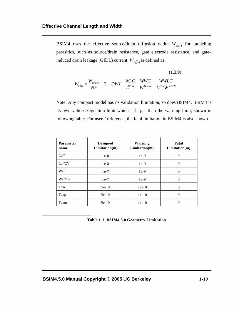
BSIM4 uses the effective source/drain diffusion width Weffcj for modeling
parasitics, such as source/drain resistance, gate electrode resistance, and gate-
induced drain leakage (GIDL) current. Weffcj is defined as
(1.3.9)
Note: Any compact model has its validation limitation, so does BSIM4. BSIM4 is
its own valid designation limit which is larger than the warning limit, shown in
following table. For users’ reference, the fatal limitation in BSIM4 is also shown.
Table 1-1. BSIM4.5.0 Geometry Limitation
Parameter name
Designed Limitation(m)
Warning Limitation(m)
Fatal Limitation(m)
Leff 1e-8 1e-9 0
LeffCV 1e-8 1e-9 0
Weff 1e-7 1e-9 0
WeffCV 1e-7 1e-9 0
Toxe 5e-10 1e-10 0
Toxp 5e-10 1e-10 0
Toxm 5e-10 1e-10 0
+++⋅−=
WWNWLNWWNWLNdrawn
effcj WLWWLC
WWWC
LWLC
DWJNF
WW 2
BSIM4.5.0 Manual Copyright © 2005 UC Berkeley 2-1
Chapter 2: Threshold Voltage Model
2.1 Long-Channel Model With Uniform Doping
Accurate modeling of threshold voltage Vth is important for precise description of
device electrical characteristics. Vth for long and wide MOSFETs with uniform
substrate doping is given by
(2.1.1)
where VFB is the flat band voltage, VTH0 is the threshold voltage of the long
channel device at zero substrate bias, and γ is the body bias coefficient given by
(2.1.2)
where Nsubstrate is the uniform substrate doping concentration.
Equation (2.1.1) assumes that the channel doping is constant and the channel
length and width are large enough. Modifications have to be made when the
substrate doping concentration is not constant and/or when the channel is short, or
narrow.
( )sbssbsssth VVTHVVFBV Φ−−Φ+=−Φ+Φ+= γγ 0
oxe
substratesi
CNqε
γ2
=
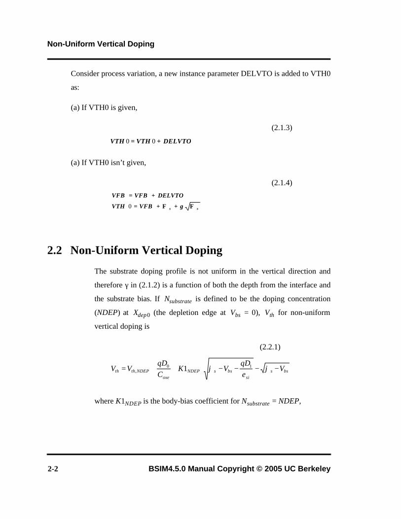
Non-Uniform Vertical Doping
2-2 BSIM4.5.0 Manual Copyright © 2005 UC Berkeley
Consider process variation, a new instance parameter DELVTO is added to VTH0
as:
(a) If VTH0 is given,
(2.1.3)
(a) If VTH0 isn’t given,
(2.1.4)
2.2 Non-Uniform Vertical Doping
The substrate doping profile is not uniform in the vertical direction and
therefore γ in (2.1.2) is a function of both the depth from the interface and
the substrate bias. If Nsubstrate is defined to be the doping concentration
(NDEP) at Xdep0 (the depletion edge at Vbs = 0), Vth for non-uniform
vertical doping is
(2.2.1)
where K1NDEP is the body-bias coefficient for Nsubstrate = NDEP,
DELVTOVTHVTH += 00
ssVFBVTH
DELVTOVFBVFB
Φ+Φ+=
+=
γ0
−−−−++= bss
sibssNDEP
oxeNDEPthth V
qDVK
CqD
VV ϕε
ϕ 10, 1
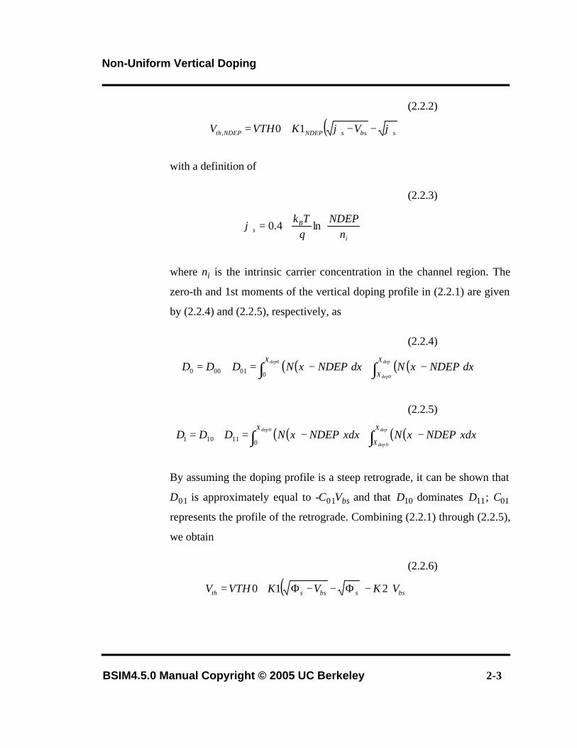
Non-Uniform Vertical Doping
BSIM4.5.0 Manual Copyright © 2005 UC Berkeley 2-3
(2.2.2)
with a definition of
(2.2.3)
where ni is the intrinsic carrier concentration in the channel region. The
zero-th and 1st moments of the vertical doping profile in (2.2.1) are given
by (2.2.4) and (2.2.5), respectively, as
(2.2.4)
(2.2.5)
By assuming the doping profile is a steep retrograde, it can be shown that
D01 is approximately equal to -C01Vbs and that D10 dominates D11; C01
represents the profile of the retrograde. Combining (2.2.1) through (2.2.5),
we obtain
(2.2.6)
( )sbssNDEPNDEPth VKVTHV ϕϕ −−+= 10,
+=
i
Bs n
NDEPqTk
ln4.0ϕ
( )( ) ( )( )∫∫ −+−=+=dep
dep
dep X
X
XdxNDEPxNdxNDEPxNDDD
0
0
001000
( )( ) ( )( )∫∫ −+−=+=dep
dep
dep X
X
XxdxNDEPxNxdxNDEPxNDDD
0
0
011101
( ) bssbssth VKVKVTHV ⋅−Φ−−Φ+= 210
Non-Uniform Vertical Doping
2-4 BSIM4.5.0 Manual Copyright © 2005 UC Berkeley
where K2 = qC01 / Coxe, and the surface potential is defined as
(2.2.7)
where
VTH0, K1, K2, and PHIN are implemented as model parameters for model
flexibility. Appendix A lists the model selectors and parameters.
Detail information on the doping profile is often available for predictive
modeling. Like BSIM3v3, BSIM4 allows K1 and K2 to be calculated based
on such details as NSUB, XT, VBX, VBM, etc. ( with the same meanings as
in BSIM3v3):
(2.2.8)
(2.2.9)
where γ1 and γ2 are the body bias coefficients when the substrate doping
concentration are equal to NDEP and NSUB, respectively:
PHINn
NDEPqTk
i
Bs +
+=Φ ln4.0
siqDPHIN ε10−=
VBMKK s −Φ−= 221 2γ
( )( )( ) VBMVBM
VBXK
sss
ss
+Φ−−ΦΦ
Φ−−Φ−=
22 21 γγ
Non-Uniform Lateral Doping: Pocket (Halo) Implant
BSIM4.5.0 Manual Copyright © 2005 UC Berkeley 2-5
(2.2.10)
(2.2.11)
VBX is the body bias when the depletion width is equal to XT, and is
determined by
(2.2.12)
2.3 Non-Uniform Lateral Doping: Pocket (Halo) Implant
In this case, the doping concentration near the source/drain junctions is
higher than that in the middle of the channel. Therefore, as channel length
becomes shorter, a Vth roll-up will usually result since the effective channel
doping concentration gets higher, which changes the body bias effect as
well. To consider these effects, Vth is written as
oxe
si
CNDEPqε
γ2
1 =
oxe
si
CNSUBqε
γ2
2 =
VBXXTqNDEP
ssi
−Φ=⋅
ε2
2
Non-Uniform Lateral Doping: Pocket (Halo) Implant
2-6 BSIM4.5.0 Manual Copyright © 2005 UC Berkeley
(2.3.1)
In addition, pocket implant can cause significant drain-induced threshold
shift (DITS) in long-channel devices [3]:
(2.3.2)
For Vds of interest, the above equation is simplified and implemented as
for tempMod = 1:
(2.3.3a)
for tempMod = 2:
(2.3.3b)
( )
seff
bseff
sbssth
LLPE
K
VKL
LPEBVKVTHV
Φ
−++
⋅−+⋅Φ−−Φ+=
10
11
2110
( ) ( )( )
+⋅+⋅−
⋅−=∆ ⋅−
−
ds
tds
VDVTPeff
effvV
tth eDVTPLLe
nvDITSV 1
/
101
ln
( ) ( )
+⋅+⋅−=∆ ⋅− dsVDVTP
eff
efftth eDVTPL
LnvDITSV 110
ln
( ) ( )
+⋅+⋅−=∆ ⋅− dsVDVTP
eff
efftnomth eDVTPL
LnvDITSV 110
ln
Short-Channel and DIBL Effects
BSIM4.5.0 Manual Copyright © 2005 UC Berkeley 2-7
Note: when tempMod =2, drain-induced threshold voltage shift (DITS)
due to pocket implant has no temperature dependence, so nominal
temperature (TNOM) is used as equation(2.3.4). when tempMod=0 or
1, equation(2.3.3) is used.
(2.3.4)
2.4 Short-Channel and DIBL Effects
As channel length becomes shorter, Vth shows a greater dependence on
channel length (SCE: short-channel effect) and drain bias (DIBL: drain-
induced barrier lowering). Vth dependence on the body bias becomes
weaker as channel length becomes shorter, because the body bias has
weaker control of the depletion region. Based on the quasi 2D solution of
the Poisson equation, Vth change due to SCE and DIBL is modeled [4]
(2.4.1)
where Vbi, known as the built-in voltage of the source/drain junctions, is
given by
(2.4.2)
( ) ( )
+⋅+⋅−=∆ ⋅− dsVDVTP
eff
efftnomth eDVTPL
LnvDITSV 110
ln
( ) ( ) ( )[ ]dssbieffthth VVLDIBLSCEV +Φ−⋅−=∆ 2, θ
⋅= 2ln
i
Bbi
nNSDNDEP
qTk
V
Short-Channel and DIBL Effects
2-8 BSIM4.5.0 Manual Copyright © 2005 UC Berkeley
where NSD is the doping concentration of source/drain diffusions. The
short-channel effect coefficient θth(Leff) in (2.4.1) has a strong dependence
on the channel length given by
(2.4.3)
lt is referred to as the characteristic length and is given by
(2.4.4)
with the depletion width Xdep equal to
(2.4.5)
Xdep is larger near the drain due to the drain voltage. Xdep / η represents the
average depletion width along the channel.
Note that in BSIM3v3 and [4], θth(Leff) is approximated with the form of
(2.4.6)
( ) ( ) 1cosh
5.0
−=
t
eff
lLeffth Lθ
ηε
⋅⋅⋅
=EPSROX
XTOXEl depsit
( )qNDEP
VX bsssi
dep−Φ
=ε2
( )
−+
−=
t
eff
t
effeffth l
L
l
LL exp2
2expθ
Short-Channel and DIBL Effects
BSIM4.5.0 Manual Copyright © 2005 UC Berkeley 2-9
which results in a phantom second Vth roll-up when Leff becomes very
small (e.g. Leff < LMIN). In BSIM4, the function form of (2.4.3) is
implemented with no approximation.
To increase the model flexibility for different technologies, several
parameters such as DVT0, DVT1, DVT2, DSUB, ETA0, and ETAB are
introduced, and SCE and DIBL are modeled separately.
To model SCE, we use
(2.4.7)
(2.4.8)
with lt changed to
(2.4.9)
To model DIBL, we use
(2.4.10)
( ) ( ) 11cosh05.0
SCE−⋅
⋅=
t
eff
lLth
DVTDVT
θ
( ) ( ) ( )sbithth VV Φ−⋅−=∆ SCESCE θ
( )bsdepsi
t VDVTEPSROX
XTOXEl ⋅+⋅
⋅⋅= 21
ε
( ) ( ) 1cosh5.0
DIBL0
−⋅=
t
eff
lLth
DSUBθ
Narrow-Width Effect
2-10 BSIM4.5.0 Manual Copyright © 2005 UC Berkeley
(2.4.11)
and lt0 is calculated by
(2.4.12)
with
(2.4.13)
DVT1 is basically equal to 1/(η)1/2. DVT2 and ETAB account for substrate
bias effects on SCE and DIBL, respectively.
2.5 Narrow-Width Effect
The actual depletion region in the channel is always larger than what is
usually assumed under the one-dimensional analysis due to the existence of
fringing fields. This effect becomes very substantial as the channel width
decreases and the depletion region underneath the fringing field becomes
comparable to the "classical" depletion layer formed from the vertical field.
The net result is an increase in Vth. This increase can be modeled as
( ) ( ) ( ) dsbsthth VVETABETAV ⋅⋅+⋅−=∆ 0DIBLDIBL θ
EPSROXXTOXE
l depsit
00
⋅⋅=
ε
qNDEPX ssi
dep
Φ=
ε20
Narrow-Width Effect
BSIM4.5.0 Manual Copyright © 2005 UC Berkeley 2-11
(2.5.1)
This formulation includes but is not limited to the inverse of channel width
due to the fact that the overall narrow width effect is dependent on process
(i.e. isolation technology). Vth change is given by
(2.5.2)
In addition, we must consider the narrow width effect for small channel
lengths. To do this we introduce the following
(2.5.3)
with ltw given by
(2.5.4)
The complete Vth model implemented in SPICE is
(2.5.5)
seffeffoxe
dep
WTOXE
WCXqNDEP
Φ=⋅
ππ
32
2max,
( ) ( ) seff
bsth WWTOXE
VBKKwidthNarrowV Φ+
⋅+=∆ − 0'331
( ) ( ) ( )sbi
lWL-th V
WDVTWDVT
widthNarrowVtw
effeffΦ−⋅
−⋅⋅
−=∆11cosh
05.02 '
( )bsdepsi
tw VWDVTEPSROX
XTOXEl ⋅+⋅
⋅⋅= 21
ε
Narrow-Width Effect
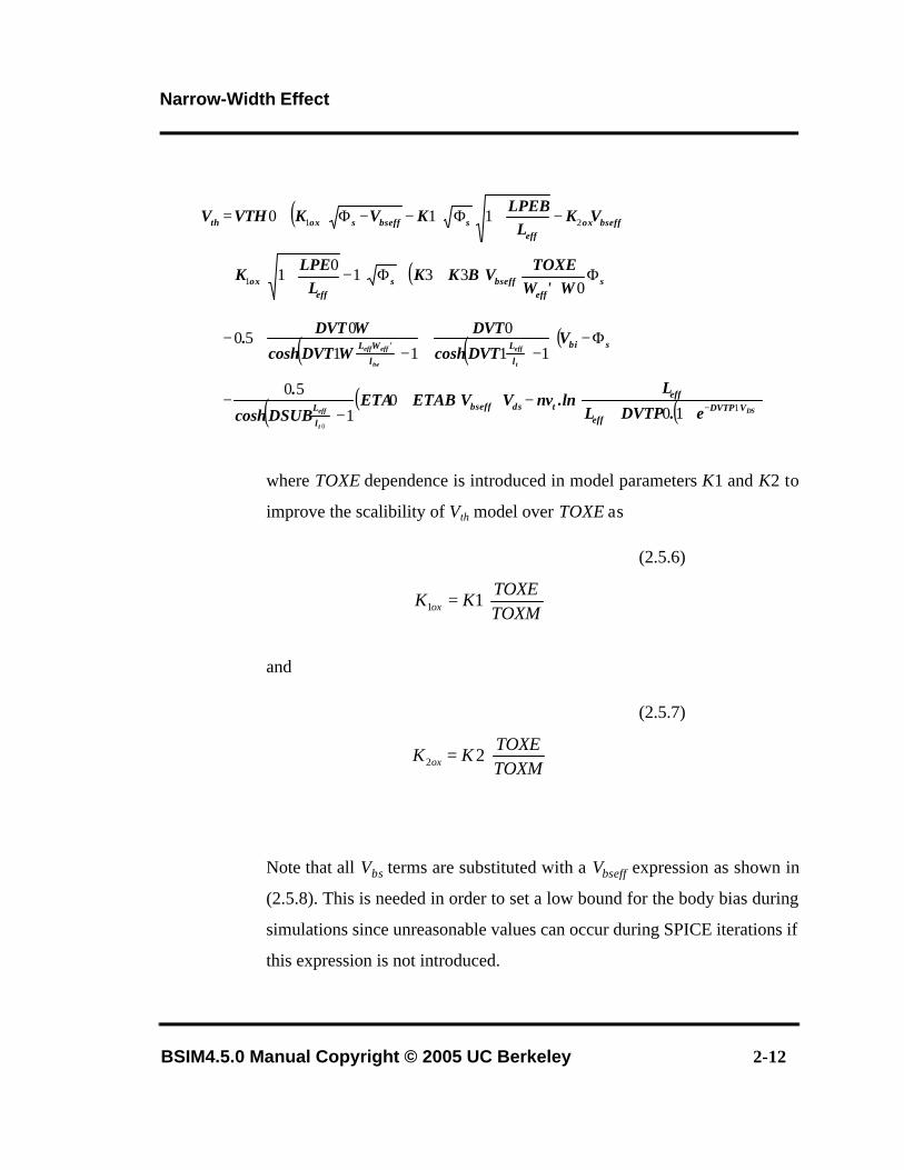
BSIM4.5.0 Manual Copyright © 2005 UC Berkeley 2-12
where TOXE dependence is introduced in model parameters K1 and K2 to
improve the scalibility of Vth model over TOXE as
(2.5.6)
and
(2.5.7)
Note that all Vbs terms are substituted with a Vbseff expression as shown in
(2.5.8). This is needed in order to set a low bound for the body bias during
simulations since unreasonable values can occur during SPICE iterations if
this expression is not introduced.
( )
( )
( ) ( ) ( )
( ) ( ) ( )
++−⋅⋅+
−−
Φ−
−+
−⋅−
Φ+
⋅++Φ
−++
−+Φ⋅−−Φ⋅+=
⋅− DS
t
eff
t
eff
tw
effeff
VDVTPeff
efftdsbseff
l
L
sbi
l
L
l
'WL
seff
bseffseff
ox
bseffoxeff
sbseffsoxth
e.DVTPL
Lln.nvVVETABETA
DSUBcosh
.
VDVTcosh
DVT
WDVTcosh
WDVT.
W'WTOXE
VBKKL
LPEK
VKL
LPEBKVKVTHV
1
1
21
100
1
50
11
0
11
050
0331
01
110
0
TOXMTOXE
KK ox ⋅= 11
TOXMTOXE
KK ox ⋅= 22
Narrow-Width Effect
BSIM4.5.0 Manual Copyright © 2005 UC Berkeley 2-13
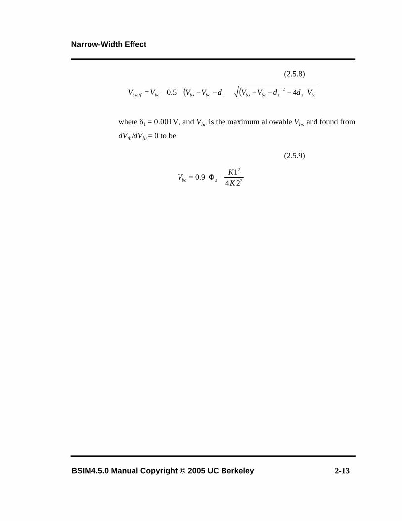
(2.5.8)
where δ1 = 0.001V, and Vbc is the maximum allowable Vbs and found from
dVth/dVbs= 0 to be
(2.5.9)
( ) ( )
⋅−−−+−−⋅+= bcbcbsbcbsbcbseff VVVVVVV 1
211 45.0 δδδ
−Φ= 2
2
241
9.0KK
V sbc
Narrow-Width Effect
2-14 BSIM4.5.0 Manual Copyright © 2005 UC Berkeley
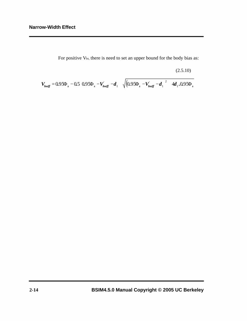
For positive Vbs, there is need to set an upper bound for the body bias as:
(2.5.10)
( )
Φ+−−Φ+−−Φ−Φ= s
'bseffs
'bseffssbseff ..V.V...V 950495095050950 1
2
11 δδδ
BSIM4.5.0 Manual Copyright © 2005 UC Berkeley 3-1
Chapter 3: Channel Charge and Subthreshold Swing Models
3.1 Channel Charge Model
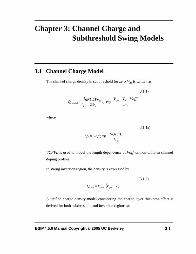
The channel charge density in subthreshold for zero Vds is written as
(3.1.1)
where
(3.1.1a)
VOFFL is used to model the length dependence of Voff’ on non-uniform channel
doping profiles.
In strong inversion region, the density is expressed by
(3.1.2)
A unified charge density model considering the charge layer thickness effect is
derived for both subthreshold and inversion regions as
−−⋅
Φ=
t
thgset
s
sichsubs nv
VoffVVv
qNDEPQ
'exp
20ε
effLVOFFL
VOFFVoff +='
( )thgseoxechs VVCQ −⋅=0
Channel Charge Model
3-2 BSIM4.5.0 Manual Copyright © 2005 UC Berkeley
(3.1.3)
where Coxeff is modeled by
(3.1.4)
and XDC is given as
(3.1.5)
In the above equations, Vgsteff, the effective (Vgse-Vth) used to describe the channel
charge densities from subthreshold to strong inversion, is modeled by
(3.1.6a)
where
(3.1.6b)
gsteffoxeffch VCQ ⋅=0
DC
sicen
cenoxe
cenoxeoxeff X
CwithCCCC
Cε
=+⋅
=
( ) 7.0
9
204
1
m109.1
Φ−−++
×=
−
TOXPVFBVTHV
Xsgsteff
DC
( )
( )( )
−−−−
Φ⋅+
−+
=∗
∗
∗
t
thgse
si
soxe
t
thgset
gsteff
nv
VoffVVm
qNDEPnCm
nv
VVmnv
V'1
exp2
exp1ln
ε
( )πMINV
marctan
5.0 +=∗
Channel Charge Model
BSIM4.5.0 Manual Copyright © 2005 UC Berkeley 3-3
MINV is introduced to improve the accuracy of Gm, Gm/Id and Gm2/Id in the
moderate inversion region.
To account for the drain bias effect, The y dependence has to be included in
(3.1.3). Consider first the case of strong inversion
(3.1.7)
VF(y) stands for the quasi-Fermi potential at any given point y along the channel
with respect to the source. (3.1.7) can also be written as
(3.1.8)
The term ∆Qchs(y) = -CoxeffAbulkVF(y) is the incremental charge density introduced
by the drain voltage at y.
In subthreshold region, the channel charge density along the channel from source
to drain can be written as
(3.1.9)
Taylor expansion of (3.1.9) yields the following (keeping the first two terms)
( ) ( )( )yVAVVCyQ Fbulkthgseoxeffchs −−⋅=
( ) ( )yQQyQ chschschs ∆+= 0
( ) ( )
−⋅=
t
Fbulkchsubschsubs nv
yVAQyQ exp0
Channel Charge Model
3-4 BSIM4.5.0 Manual Copyright © 2005 UC Berkeley
(3.1.10)
Similarly, (3.1.10) is transformed into
(3.1.11)
where ∆Qchsubs(y) is the incremental channel charge density induced by the drain
voltage in the subthreshold region. It is written as
(3.1.12)
To obtain a unified expression for the incremental channel charge density ∆Qch(y)
induced by Vds, we assume ∆Qch(y) to be
(3.1.13)
Substituting ∆Qch(y) of (3.1.8) and (3.1.12) into (3.1.13), we obtain
(3.1.14)
( ) ( )
−=
t
Fbulkchsubschsubs nv
yVAQyQ 10
( ) ( )yQQyQ chsubschsubschsubs ∆+= 0
( ) ( )t
Fbulkchsubschsubs nv
yVAQyQ ⋅−=∆ 0
( ) ( ) ( )( ) ( )yQyQ
yQyQyQ
chsubschs
chsubschsch ∆+∆
∆⋅∆=∆
( ) ( )0ch
b
Fch Q
VyV
yQ −=∆
Subthreshold Swing n
BSIM4.5.0 Manual Copyright © 2005 UC Berkeley 3-5
where Vb = (Vgsteff + nvt) / Abulk. In the model implementation, n of Vb is replaced
by a typical constant value of 2. The expression for Vb now becomes
(3.1.15)
A unified expression for Qch(y) from subthreshold to strong inversion regions is
(3.1.16)
3.2 Subthreshold Swing n
The drain current equation in the subthreshold region can be expressed as
(3.2.1)
where
(3.2.2)
vt is the thermal voltage and equal to kBT/q. Voff’ = VOFF + VOFFL / Leff is the
offset voltage, which determines the channel current at Vgs = 0. In (3.2.1), n is the
VV v
Ab
gsteff t
bulk= +2
( ) ( )
−⋅⋅=
b
Fgsteffoxeffch V
yVVCyQ 1
−−⋅
−−=
t
offthgs
t
dsds nv
VVVv
VII
'expexp10
20 2 t
s
si vNDEPq
LW
IΦ
=ε
µ
Subthreshold Swing n
3-6 BSIM4.5.0 Manual Copyright © 2005 UC Berkeley
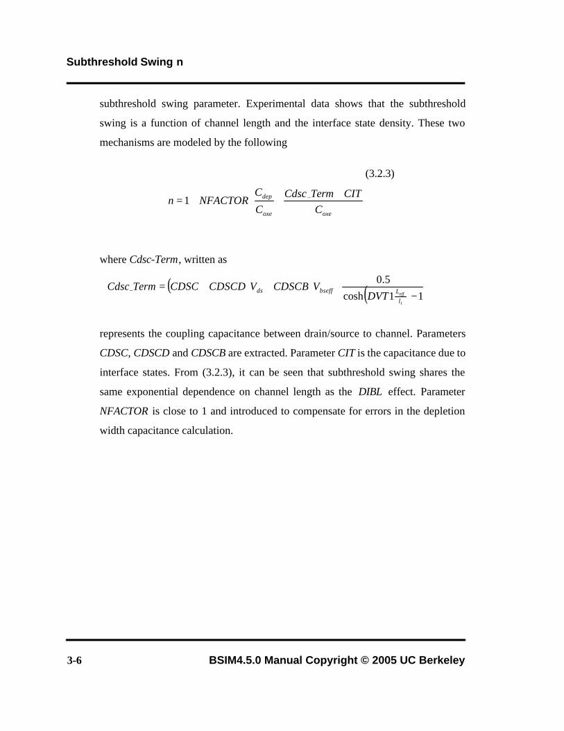
subthreshold swing parameter. Experimental data shows that the subthreshold
swing is a function of channel length and the interface state density. These two
mechanisms are modeled by the following
(3.2.3)
where Cdsc-Term, written as
represents the coupling capacitance between drain/source to channel. Parameters
CDSC, CDSCD and CDSCB are extracted. Parameter CIT is the capacitance due to
interface states. From (3.2.3), it can be seen that subthreshold swing shares the
same exponential dependence on channel length as the DIBL effect. Parameter
NFACTOR is close to 1 and introduced to compensate for errors in the depletion
width capacitance calculation.
oxeoxe
dep
CCITTermCdsc
C
CNFACTORn
++⋅+= −1
( ) ( ) 11cosh5.0
−⋅⋅+⋅+=−
t
eff
lLbseffds
DVTVCDSCBVCDSCDCDSCTermCdsc
BSIM4.5.0 Manual Copyright © 2005 UC Berkeley 4-1
Chapter 4: Gate Direct Tunneling Current Model
As the gate oxide thickness is scaled down to 3nm and below, gate leakage current
due to carrier direct tunneling becomes important. This tunneling happens between
the gate and silicon beneath the gate oxide. To reduce the tunneling current, high-k
dielectrics are being studied to replace gate oxide. In order to maintain a good
interface with substrate, multi-layer dielectric stacks are being proposed. The
BSIM4 gate tunneling model has been shown to work for multi-layer gate stacks
as well. The tunneling carriers can be either electrons or holes, or both, either from
the conduction band or valence band, depending on (the type of the gate and) the
bias regime.
In BSIM4, the gate tunneling current components include the tunneling current
between gate and substrate (Igb), and the current between gate and channel (Igc),
which is partitioned between the source and drain terminals by Igc = Igcs + Igcd.
Model selectors
4-2 BSIM4.5.0 Manual Copyright © 2005 UC Berkeley
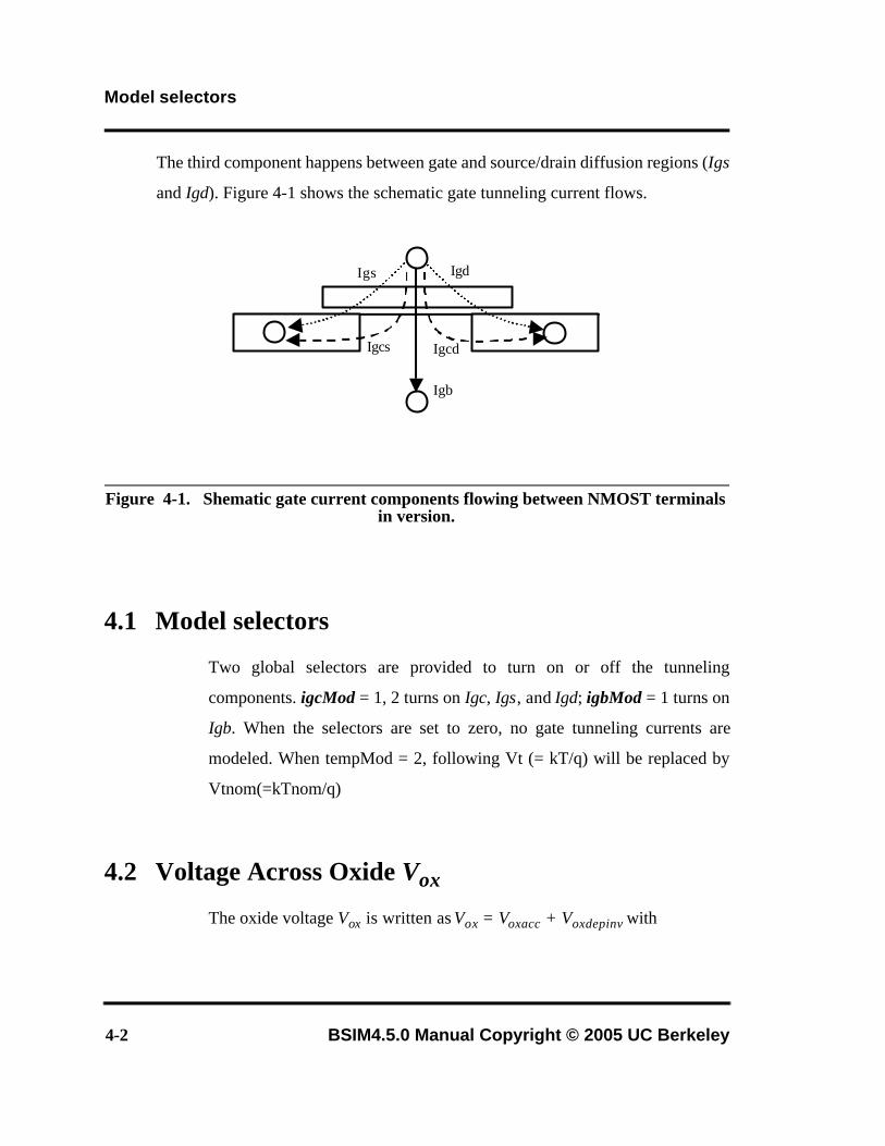
The third component happens between gate and source/drain diffusion regions (Igs
and Igd). Figure 4-1 shows the schematic gate tunneling current flows.
Figure 4-1. Shematic gate current components flowing between NMOST terminals in version.
4.1 Model selectors
Two global selectors are provided to turn on or off the tunneling
components. igcMod = 1, 2 turns on Igc, Igs, and Igd; igbMod = 1 turns on
Igb. When the selectors are set to zero, no gate tunneling currents are
modeled. When tempMod = 2, following Vt (= kT/q) will be replaced by
Vtnom(=kTnom/q)
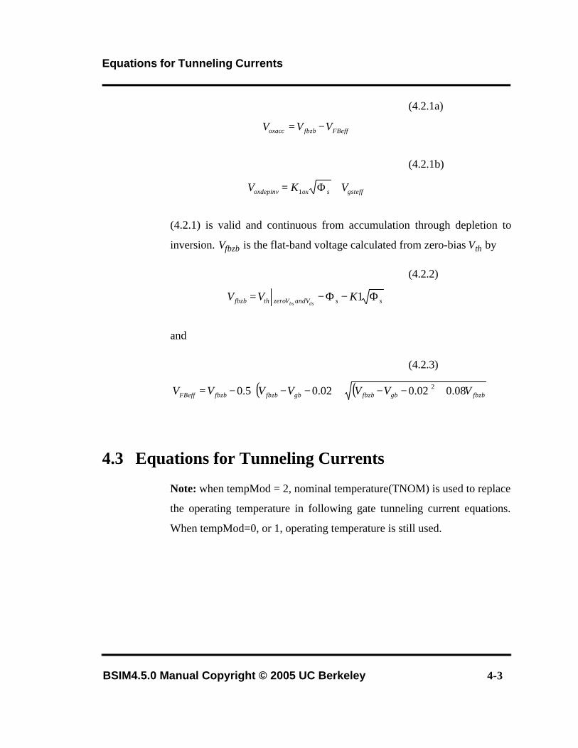
4.2 Voltage Across Oxide Vox
The oxide voltage Vox is written as Vox = Voxacc + Voxdepinv with
Igs Igd
Igb
Igcs Igcd
Equations for Tunneling Currents
BSIM4.5.0 Manual Copyright © 2005 UC Berkeley 4-3
(4.2.1a)
(4.2.1b)
(4.2.1) is valid and continuous from accumulation through depletion to
inversion. Vfbzb is the flat-band voltage calculated from zero-bias Vth by
(4.2.2)
and
(4.2.3)
4.3 Equations for Tunneling Currents
Note: when tempMod = 2, nominal temperature(TNOM) is used to replace
the operating temperature in following gate tunneling current equations.
When tempMod=0, or 1, operating temperature is still used.
FBefffbzboxacc VVV −=
gsteffsoxoxdepinv VKV +Φ= 1
ssVandVzerothfbzb KVVdsbs
Φ−Φ−= 1
( ) ( )
+−−+−−−= fbzbgbfbzbgbfbzbfbzbFBeff VVVVVVV 08.002.002.05.0 2
Equations for Tunneling Currents
4-4 BSIM4.5.0 Manual Copyright © 2005 UC Berkeley
4.3.1 Gate-to-Substrate Current ( Igb = Igbacc + Igbinv)
Igbacc, determined by ECB (Electron tunneling from Conduction Band), is
significant in accumulation and given by
(4.3.1)
where the physical constants A = 4.97232e-7 A/V2, B = 7.45669e11 (g/F-
s2)0.5, and
Igbinv, determined by EVB (Electron tunneling from Valence Band), is
significant in inversion and given by
(4.3.2)
where A = 3.75956e-7 A/V2, B = 9.82222e11 (g/F-s2)0.5, and
( ) ( )[ ]oxaccoxacc
auxgboxRatioeffeff
VCIGBACCVBIGBACCAIGBACCTOXEB
VVTALWIgbacc
⋅+⋅⋅−⋅−⋅
⋅⋅⋅⋅=
1exp
2
1TOXETOXE
TOXREFT
NTOX
oxRatio ⋅
=
⋅
−−+⋅⋅=
t
fbzbgbtaux vNIGBACC
VVvNIGBACCV exp1log
( ) ( )[ ]oxdepinvoxdepinv
auxgboxRatioeffeff
VCIGBINVVBIGBINVAIGBINVTOXEB
VVTALWIgbinv
⋅+⋅⋅−⋅−⋅
⋅⋅⋅⋅=
1exp
Equations for Tunneling Currents
BSIM4.5.0 Manual Copyright © 2005 UC Berkeley 4-5
4.3.2 Gate-to-Channel Current (Igc0) and Gate-to-S/D (Igs and Igd)
Igc0, determined by ECB for NMOS and HVB (Hole tunneling from
Valence Band) for PMOS at Vds=0, is formulated as
(4.3.3)
where A = 4.97232 A/V2 for NMOS and 3.42537 A/V2 for PMOS, B =
7.45669e11 (g/F-s2)0.5 for NMOS and 1.16645e12 (g/F-s2)0.5 for PMOS,
and for igcMod = 1:
for igcMod = 2:
Igs and Igd -- Igs represents the gate tunneling current between the gate
and the source diffusion region, while Igd represents the gate tunneling
current between the gate and the drain diffusion region. Igs and Igd are
determined by ECB for NMOS and HVB for PMOS, respectively.
⋅
−+⋅⋅=
t
oxdepinvtaux vNIGBINV
EIGBINVVvNIGBINVV exp1log
( ) ( )[ ]oxdepinvoxdepinv
auxgseoxRatioeffeff
VCIGCVBIGCAIGCTOXEBexp
VVTALWIgc
⋅+⋅⋅−⋅−⋅
⋅⋅⋅⋅=
1
0
⋅
−+⋅⋅=
t
gsetaux vNIGC
VTHVvNIGCV
0exp1log
⋅
−+⋅⋅=
t
gsetaux vNIGC
VTHVvNIGCV explog 1
Equations for Tunneling Currents
4-6 BSIM4.5.0 Manual Copyright © 2005 UC Berkeley
(4.3.4)
and
(4.3.5)
where A = 4.97232 A/V2 for NMOS and 3.42537 A/V2 for PMOS, B =
7.45669e11 (g/F-s2)0.5 for NMOS and 1.16645e12 (g/F-s2)0.5 for PMOS,
and
Vfbsd is the flat-band voltage between gate and S/D diffusions calculated as
If NGATE > 0.0
Else Vfbsd = 0.0.
( ) ( )[ ]''
'
1exp gsgs
gsgseoxRatioEdgeff
VCIGSDVBIGSDAIGSDPOXEDGETOXEB
VVTADLCIGWIgs
⋅+⋅⋅−⋅⋅⋅−⋅
⋅⋅⋅⋅=
( ) ( )[ ]''
'
1exp gdgd
gdgdeoxRatioEdgeff
VCIGSDVBIGSDAIGSDPOXEDGETOXEB
VVTADLCIGWIgd
⋅+⋅⋅−⋅⋅⋅−⋅
⋅⋅⋅⋅=
( )2
1POXEDGETOXEPOXEDGETOXE
TOXREFT
NTOX
eoxRatioEdg ⋅⋅
⋅=
( ) 40.12' −+−= eVVV fbsdgsgs
( ) 40.12' −+−= eVVV fbsdgdgd
VFBSDOFFNSD
NGATElogqTk
V Bfbsd +
=
Equations for Tunneling Currents
BSIM4.5.0 Manual Copyright © 2005 UC Berkeley 4-7
4.3.3 Partition of Igc
To consider the drain bias effect, Igc is split into two components, Igcs and
Igcd, that is Igc = Igcs + Igcd, and
(4.3.6)
and
(4.3.7)
Where Igc0 is Igc at Vds=0.
If the model parameter PIGCD is not specified, it is given by
(4.3.8)
( )4e0.2
4e0.11exp0 22 −+⋅
−+−⋅−+⋅⋅=
dseff
dseffdseff
VPIGCD
VPIGCDVPIGCDIgcIgcs
( ) ( )4e0.2
4e0.1exp110 22 −+⋅
−+⋅−⋅+⋅−⋅=
dseff
dseffdseff
VPIGCD
VPIGCDVPIGCDIgcIgcd
⋅−
⋅=
gsteff
dseff
gsteff V
V
VTOXEB
PIGCD2
12
BSIM4.5.0 Manual Copyright © 2005 UC Berkeley 5-1
Chapter 5: Drain Current Model
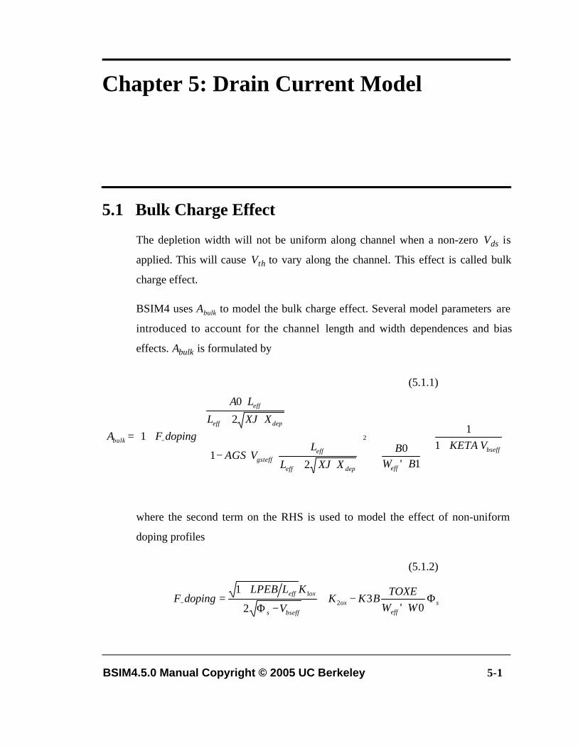
5.1 Bulk Charge Effect
The depletion width will not be uniform along channel when a non-zero Vds is
applied. This will cause Vth to vary along the channel. This effect is called bulk
charge effect.
BSIM4 uses Abulk to model the bulk charge effect. Several model parameters are
introduced to account for the channel length and width dependences and bias
effects. Abulk is formulated by
(5.1.1)
where the second term on the RHS is used to model the effect of non-uniform
doping profiles
(5.1.2)
bseff
effdepeff
effgsteff
depeff
eff
bulk VKETA
BWB
XXJL
LVAGS
XXJL
LA
dopingFA⋅+
⋅
++
⋅+⋅−
⋅⋅+
⋅
⋅+= − 11
1'0
21
2
0
1 2
seff
oxbseffs
oxeff
WWTOXE
BKKV
KLLPEBdopingF Φ
+−+
−Φ
+=− 0'
32
12
1
Unified Mobility Model
5-2 BSIM4.5.0 Manual Copyright © 2005 UC Berkeley
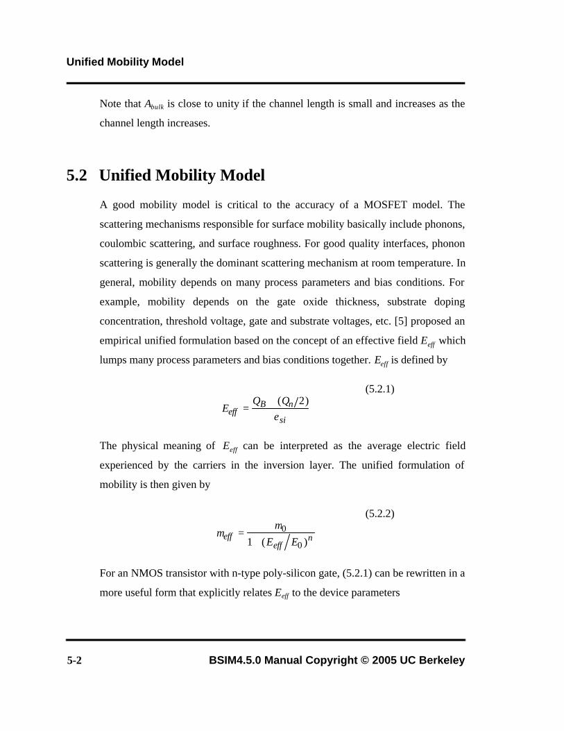
Note that Abulk is close to unity if the channel length is small and increases as the
channel length increases.
5.2 Unified Mobility Model
A good mobility model is critical to the accuracy of a MOSFET model. The
scattering mechanisms responsible for surface mobility basically include phonons,
coulombic scattering, and surface roughness. For good quality interfaces, phonon
scattering is generally the dominant scattering mechanism at room temperature. In
general, mobility depends on many process parameters and bias conditions. For
example, mobility depends on the gate oxide thickness, substrate doping
concentration, threshold voltage, gate and substrate voltages, etc. [5] proposed an
empirical unified formulation based on the concept of an effective field Eeff which
lumps many process parameters and bias conditions together. Eeff is defined by
(5.2.1)
The physical meaning of Eeff can be interpreted as the average electric field
experienced by the carriers in the inversion layer. The unified formulation of
mobility is then given by
(5.2.2)
For an NMOS transistor with n-type poly-silicon gate, (5.2.1) can be rewritten in a
more useful form that explicitly relates Eeff to the device parameters
EQ Q
effB n
si=
+ ( )2ε
µµ
νeffeffE E
=+
0
01 ( )
Unified Mobility Model
BSIM4.5.0 Manual Copyright © 2005 UC Berkeley 5-3
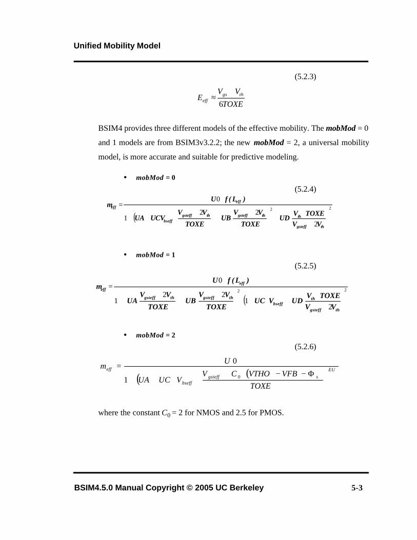
(5.2.3)
BSIM4 provides three different models of the effective mobility. The mobMod = 0
and 1 models are from BSIM3v3.2.2; the new mobMod = 2, a universal mobility
model, is more accurate and suitable for predictive modeling.
• mobMod = 0
(5.2.4)
• mobMod = 1
(5.2.5)
• mobMod = 2
(5.2.6)
where the constant C0 = 2 for NMOS and 2.5 for PMOS.
TOXE
VVE thgs
eff 6
+≈
( )22
2
221
0
+⋅
+
++
+++
⋅=
thgsteff
ththgsteffthgsteffbseff
effeff
VVTOXEV
UDTOXE
VVUB
TOXE
VVUCVUA
)L(fUµ
( )22
21
221
0
+⋅
+⋅+
++
++
⋅=
thgsteff
thbseff
thgsteffthgsteff
effeff
VVTOXEV
UDVUCTOXE
VVUB
TOXE
VVUA
)L(fUµ
( ) ( ) EUsgsteff
bseff
eff
TOXEVFBVTHOCV
VUCUA
U
Φ−−⋅+⋅++
=01
0µ
Asymmetric and Bias-Dependent Source/Drain Resistance Model
5-4 BSIM4.5.0 Manual Copyright © 2005 UC Berkeley
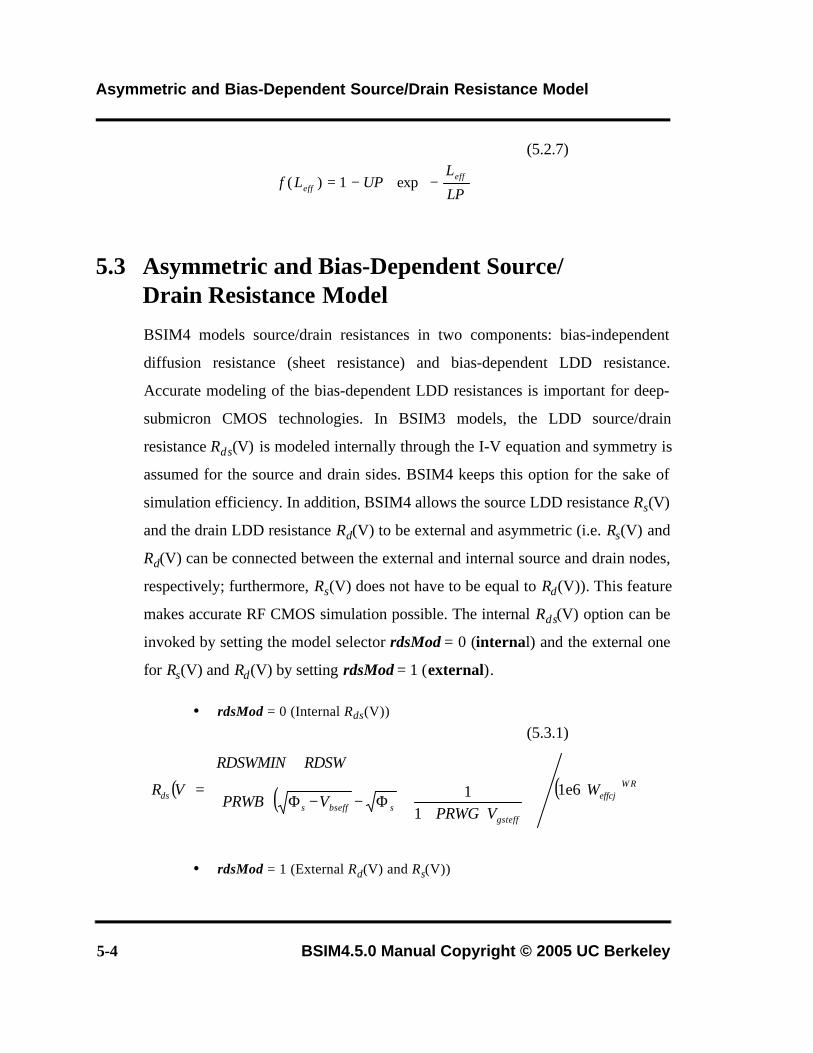
(5.2.7)
5.3 Asymmetric and Bias-Dependent Source/Drain Resistance Model
BSIM4 models source/drain resistances in two components: bias-independent
diffusion resistance (sheet resistance) and bias-dependent LDD resistance.
Accurate modeling of the bias-dependent LDD resistances is important for deep-
submicron CMOS technologies. In BSIM3 models, the LDD source/drain
resistance Rds(V) is modeled internally through the I-V equation and symmetry is
assumed for the source and drain sides. BSIM4 keeps this option for the sake of
simulation efficiency. In addition, BSIM4 allows the source LDD resistance Rs(V)
and the drain LDD resistance Rd(V) to be external and asymmetric (i.e. Rs(V) and
Rd(V) can be connected between the external and internal source and drain nodes,
respectively; furthermore, Rs(V) does not have to be equal to Rd(V)). This feature
makes accurate RF CMOS simulation possible. The internal Rds(V) option can be
invoked by setting the model selector rdsMod = 0 (internal) and the external one
for Rs(V) and Rd(V) by setting rdsMod = 1 (external).
• rdsMod = 0 (Internal Rds(V))
(5.3.1)
• rdsMod = 1 (External Rd(V) and Rs(V))
−⋅−=
LP
LUPLf eff
eff exp1)(
( ) ( ) ( )W Reffcj
gsteffsbseffs
ds WVPRWG
VPRWB
RDSWRDSWMIN
VR ⋅
⋅++Φ−−Φ⋅
⋅+
= 1e61
1
Asymmetric and Bias-Dependent Source/Drain Resistance Model
BSIM4.5.0 Manual Copyright © 2005 UC Berkeley 5-5
(5.3.2)
(5.3.3)
Vfbsd is the calculated flat-band voltage between gate and source/drain as given in
Section 4.3.2.
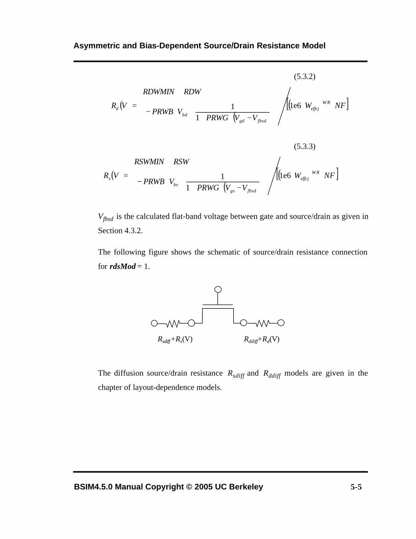
The following figure shows the schematic of source/drain resistance connection
for rdsMod = 1.
The diffusion source/drain resistance Rsdiff and Rddiff models are given in the
chapter of layout-dependence models.
( )( )
( )[ ]NFWVVPRWG
VPRWB
RDWRDWMIN
VR W Reffcj
fbsdgdbd
d ⋅⋅
−⋅++⋅−
⋅+
= 1e61
1
( )( )
( )[ ]NFWVVPRWG
VPRWB
RSWRSWMIN
VR W Reffcj
fbsdgsbs
s ⋅⋅
−⋅++⋅−
⋅+
= 1e61
1
Rsdiff+Rs(V) Rddiff+Rd(V)
Drain Current for Triode Region
5-6 BSIM4.5.0 Manual Copyright © 2005 UC Berkeley
5.4 Drain Current for Triode Region
5.4.1 Rds(V)=0 or rdsMod=1 (“intrinsic case”)
Both drift and diffusion currents can be modeled by
(5.4.1)
where une(y) can be written as
(5.4.2)
Substituting (5.4.2) in (5.4.1), we get
(5.4.3)
(5.4.3) is integrated from source to drain to get the expression for linear
drain current. This expression is valid from the subthreshold regime to the
strong inversion regime
( ) ( ) ( ) ( )dy
ydVyyWQyI F
nechds µ=
µ µne y
eff
y
sat
EE
( ) =+1
( ) ( ) ( )dy
ydV
EEV
yVWQyI F
sat
y
eff
b
Fchds
+
−=
110
µ
Velocity Saturation
BSIM4.5.0 Manual Copyright © 2005 UC Berkeley 5-7
(5.4.4)
5.4.2 Rds(V) > 0 and rdsMod=0 (“Extrinsic case”)
The drain current in this case is expressed by
(5.4.5)
5.5 Velocity Saturation
Velocity saturation is modeled by [5]
(5.5.1)
where Esat corresponds to the critical electrical field at which the carrier velocity
becomes saturated. In order to have a continuous velocity model at E = Esat, Esat
must satisfy
+
−
=
LEV
L
VV
VQWI
sat
ds
b
dsdscheff
ds
1
210
0
µ
IIR I
V
dsdso
ds dso
ds
=+1
sat
satsat
eff
EEVSAT
EEEEE
v
≥=
<+
=1
µ
Saturation Voltage Vdsat
5-8 BSIM4.5.0 Manual Copyright © 2005 UC Berkeley
(5.5.2)
5.6 Saturation Voltage Vdsat
5.6.1 Intrinsic case
In this case, the LDD source/drain resistances are either zero or non zero
but not modeled inside the intrinsic channel region. It is easy to obtain Vdsat
as [7]
(5.6.1)
5.6.2 Extrinsic Case
In this case, non-zero LDD source/drain resistance Rds(V) is modeled
internally through the I-V equation and symetry is assumed for the source
and drain sides. Vdsat is obtained as [7]
(5.6.2a)
where
effsat
VSATE
µ2
=
VE L V v
A E L V vdsat
sat gsteff t
bulk sat gsteff t=
++ +
( )22
Vb b ac
adsat =
− − −2 42

Saturation Voltage Vdsat
BSIM4.5.0 Manual Copyright © 2005 UC Berkeley 5-9
(5.6.2b)
(5.6.2c)
(5.6.2d)
(5.6.2e)
λ is introduced to model the non-saturation effects which are found for
PMOSFETs.
5.6.3 Vdseff Formulation
An effective Vds, Vdseff, is used to ensure a smooth transition near Vdsat
from trode to saturation regions. Vdseff is formulated as
(5.6.3)
where δ (DELTA) is a model parameter.
−+= 1
12
λbulkdsoxeeffbulk ARVSATCWAa
( )( )
++
+
−+
−=
dsoxeefftgsteffbulk
effsatbulktgsteff
RVSATCWvVA
LEAvVb
23
12
2λ
( ) ( ) dsoxeefftgsteffeffsattgsteff RVSATCWvVLEvVc 2222 +++=
21 AVA gsteff +=λ
( ) ( )
⋅+−−+−−−= dsatdsdsatdsdsatdsatdseff VVVVVVV δδδ 4
21 2
Saturation-Region Output Conductance Model
5-10 BSIM4.5.0 Manual Copyright © 2005 UC Berkeley
5.7 Saturation-Region Output Conductance Model
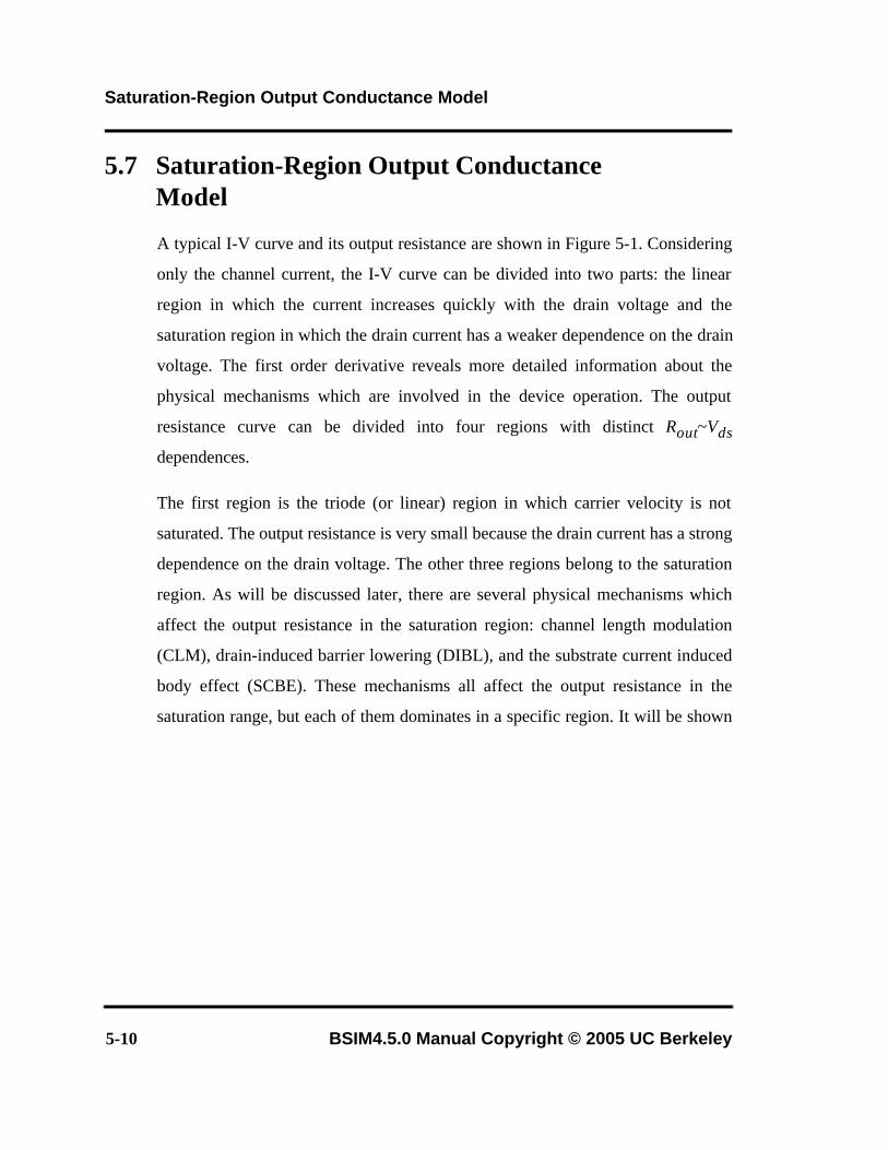
A typical I-V curve and its output resistance are shown in Figure 5-1. Considering
only the channel current, the I-V curve can be divided into two parts: the linear
region in which the current increases quickly with the drain voltage and the
saturation region in which the drain current has a weaker dependence on the drain
voltage. The first order derivative reveals more detailed information about the
physical mechanisms which are involved in the device operation. The output
resistance curve can be divided into four regions with distinct Rout~Vds
dependences.
The first region is the triode (or linear) region in which carrier velocity is not
saturated. The output resistance is very small because the drain current has a strong
dependence on the drain voltage. The other three regions belong to the saturation
region. As will be discussed later, there are several physical mechanisms which
affect the output resistance in the saturation region: channel length modulation
(CLM), drain-induced barrier lowering (DIBL), and the substrate current induced
body effect (SCBE). These mechanisms all affect the output resistance in the
saturation range, but each of them dominates in a specific region. It will be shown
Saturation-Region Output Conductance Model
BSIM4.5.0 Manual Copyright © 2005 UC Berkeley 5-11
next that CLM dominates in the second region, DIBL in the third region, and
SCBE in the fourth region.
Figure 5-1. General behavior of MOSFET output resistance.
The channel current is a function of the gate and drain voltage. But the current
depends on the drain voltage weakly in the saturation region. In the following, the
Early voltage is introduced for the analysis of the output resistance in the
saturation region:
(5.7.1)
0 1 2 3 40.0
0.5
1.0
1.5
2.0
2.5
3.0
SCBE
Rout (K
Ohm
s)
DIBLCLMTriodeI ds
(m
A)
Vds (V)
0
2
4
6
8
10
12
14
( ) ( ) ( )
( )
⋅+⋅=
⋅∂
∂+=
∫
∫
d
V
VA
dsatgsdsat
d
V
Vd
dsgsdsdsatgsdsatdsgsds
dVV
VVI
dVV
VVIVVIVVI
ds
dsat
ds
dsat
11,
,,,
Saturation-Region Output Conductance Model
BSIM4.5.0 Manual Copyright © 2005 UC Berkeley 5-12
where the Early voltage VA is defined as
(5.7.2)
We assume in the following analysis that the contributions to the Early voltage
from all mechanisms are independent and can be calculated separately.
5.7.1 Channel Length Modulation (CLM)
If channel length modulation is the only physical mechanism to be taken
into account, the Early voltage can be calculated by
(5.7.3)
Based on quasi two-dimensional analysis and through integration, we
propose VACLM to be
(5.7.4)
where
(5.7.5)
( ) 1,
−
∂
∂⋅=
d
dsgsdsdsatA V
VVIIV
( ) 1,
−
∂∂
⋅∂
∂⋅=
d
dsgsdsdsatACLM V
LL
VVIIV
( )dsatdsclmACLM VVCV −⋅=
litlEV
LV
IRLE
VPVAGF
PCLMC
sat
dsateff
dseff
dsods
effsat
gsteffclm
111
1⋅
+
⋅+
+⋅⋅=
Saturation-Region Output Conductance Model
BSIM4.5.0 Manual Copyright © 2005 UC Berkeley 5-13
and the F factor to account for the impact of pocket implant technology is
(5.7.6)
and litl in (5.7.5) is given by
(5.7.7)
PCLM is introduced into VACLM to compensate for the error caused by XJ
since the junction depth XJ can not be determined very accurately.
5.7.2 Drain-Induced Barrier Lowering (DIBL)
The Early voltage VADIBLC due to DIBL is defined as
(5.7.8)
Vth has a linear dependence on Vds. As channel length decreases, VADIBLC
decreases very quickly
(5.7.9)
tgsteff
eff
vV
LFPROUT
F
21
1
+⋅+
=
EPSROXXJTOXE
litl si ⋅=
ε
( ) 1,
−
∂∂
⋅∂
∂⋅=
d
th
th
dsgsdsdsatADIBL V
VV
VVIIV
( )
+⋅
++−
⋅++
=effsat
gsteff
tgsteffdsatbulk
dsatbulk
bseffrout
tgsteffADIBL LE
VPVAG
vVVAVA
VPDIBLCBvV
V 12
11
2θ
Saturation-Region Output Conductance Model
BSIM4.5.0 Manual Copyright © 2005 UC Berkeley 5-14
where θrout has a similar dependence on the channel length as the DIBL
effect in Vth, but a separate set of parameters are used:
(5.7.10)
Parameters PDIBLC1, PDIBLC2, PDIBLCB and DROUT are introduced to
correct the DIBL effect in the strong inversion region. The reason why
DVT0 is not equal to PDIBLC1 and DVT1 is not equal to DROUT is
because the gate voltage modulates the DIBL effect. When the threshold
voltage is determined, the gate voltage is equal to the threshold voltage.
But in the saturation region where the output resistance is modeled, the
gate voltage is much larger than the threshold voltage. Drain induced
barrier lowering may not be the same at different gate bias. PDIBLC2 is
usually very small. If PDIBLC2 is put into the threshold voltage model, it
will not cause any significant change. However it is an important parameter
in VADIBLC for long channel devices, because PDIBLC2 will be dominant if
the channel is long.
5.7.3 Substrate Current Induced Body Effect (SCBE)
When the electrical field near the drain is very large (> 0.1MV/cm), some
electrons coming from the source (in the case of NMOSFETs) will be
energetic (hot) enough to cause impact ionization. This will generate
electron-hole pairs when these energetic electrons collide with silicon
atoms. The substrate current Isub thus created during impact ionization will
( ) 22cosh2
1
0
LCPDIBPDIBLC
ltLDROUTrout eff
+−
= ⋅θ
Saturation-Region Output Conductance Model
BSIM4.5.0 Manual Copyright © 2005 UC Berkeley 5-15
increase exponentially with the drain voltage. A well known Isub model [8]
is
(5.7.11)
Parameters Ai and Bi are determined from measurement. Isub affects the
drain current in two ways. The total drain current will change because it is
the sum of the channel current as well as the substrate current. The total
drain current can now be expressed as follows
(5.7.12)
The Early voltage due to the substrate current VASCBE can therefore be
calculated by
(5.7.13)
We can see that VASCBE is a strong function of Vds. In addition, we also
observe that VASCBE is small only when Vds is large. This is why SCBE is
important for devices with high drain voltage bias. The channel length and
gate oxide dependence of VASCBE comes from Vdsat and litl. We replace Bi
with PSCBE2 and Ai/Bi with PSCBE1/Leff to get the following expression
for VASCBE
( )
−⋅
−−=dsatds
idsatdsds
i
isub VV
litlBVVI
BA
I exp
( )
−+⋅=+=
−⋅−−−−
dsatds
i
i
iVVlitlB
AB
dsatdsIsubowdssubIsubowdsds
VVIIII
exp1//
−⋅
=dsatds
i
i
iASCBE VV
litlBAB
V exp
Single-Equation Channel Current Model
BSIM4.5.0 Manual Copyright © 2005 UC Berkeley 5-16
(5.7.14)
5.7.4 Drain-Induced Threshold Shift (DITS) by Pocket Implant
It has been shown that a long-channel device with pocket implant has a
smaller Rout than that of uniformly-doped device [3]. The Rout degradation
factor F is given in (5.7.6). In addition, the pocket implant introduces a
potential barrier at the drain end of the channel. This barrier can be lowered
by the drain bias even in long-channel devices. The Early voltage due to
DITS is modeled by
(5.7.15)
5.8 Single-Equation Channel Current Model
The final channel current equation for both linear and saturation regions now
becomes
(5.8.1)
where NF is the number of device fingers, and
−
⋅−=
dsatdseffASCBE VVlitlPSCBE
LEPSCB
V1
exp21
( ) ( )[ ]dseffADITS VPDITSDLPDITSLFPDITS
V ⋅⋅++⋅⋅= exp111
−+⋅
−+⋅
−+⋅
+
+⋅
=ASCBE
dseffds
ADITS
dseffds
ADIBL
dseffds
Asat
A
clmVIR
dsds V
VV
V
VV
V
VV
VV
CNFI
Idseff
dsds111ln
11
1 0
0
New Current Saturation Mechanisms: Velocity Overshoot and Source End
BSIM4.5.0 Manual Copyright © 2005 UC Berkeley 5-17
(5.8.2)
VA is written as
(5.8.3)
where VAsat is
(5.8.4)
VAsat is the Early voltage at Vds = Vdsat. VAsat is needed to have continuous drain
current and output resistance expressions at the transition point between linear and
saturation regions.
5.9 New Current Saturation Mechanisms: Velocity Overshoot and Source End Velocity Limit Model
5.9.1 Velocity Overshoot
In the deep-submicron region, the velocity overshoot has been observed to
be a significant effect even though the supply voltage is scaled down
ACLMAsatA VVV +=
( )[ ]λ2
22
1
12
+−
−⋅++= +
bulkeffoxeds
vVVA
gsteffeffoxedsdsateffsat
Asat AWvsatCR
VWvsatCRVLEV tgsteff
dsatbulk
New Current Saturation Mechanisms: Velocity Overshoot and Source End
BSIM4.5.0 Manual Copyright © 2005 UC Berkeley 5-18
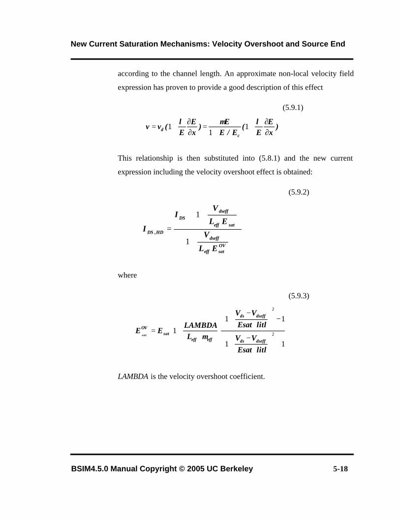
according to the channel length. An approximate non-local velocity field
expression has proven to provide a good description of this effect
(5.9.1)
This relationship is then substituted into (5.8.1) and the new current
expression including the velocity overshoot effect is obtained:
(5.9.2)
where
(5.9.3)
LAMBDA is the velocity overshoot coefficient.
)xE
E(
E/EE
)xE
E(vv
cd ∂
∂+
+=
∂∂
+=λµλ
11
1
OVsateff
dseff
sateff
dseffDS
HD,DS
EL
V
EL
VI
I
+
+⋅
=1
1
+
⋅
−+
−
⋅
−+
⋅⋅
+=
11
111 2
2
litlEsatVV
litlEsatVV
LLAMBDA
EEdseffds
dseffds
effeffsat
OVsa t µ
New Current Saturation Mechanisms: Velocity Overshoot and Source End
BSIM4.5.0 Manual Copyright © 2005 UC Berkeley 5-19
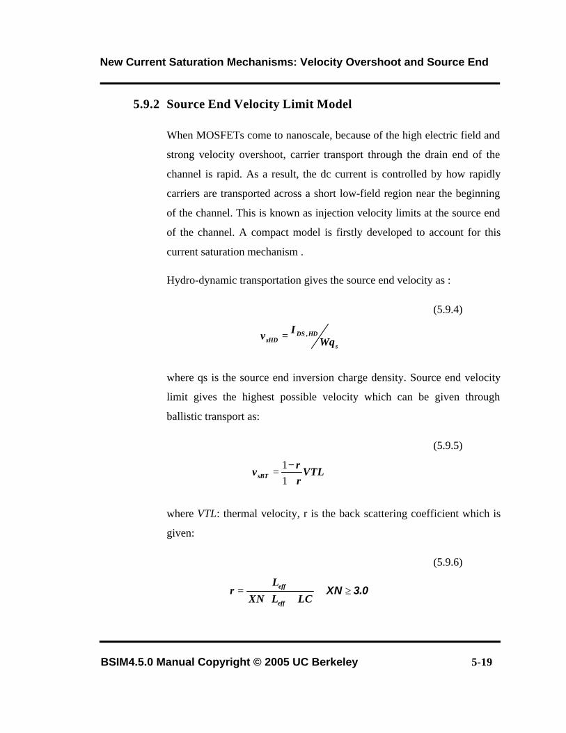
5.9.2 Source End Velocity Limit Model
When MOSFETs come to nanoscale, because of the high electric field and
strong velocity overshoot, carrier transport through the drain end of the
channel is rapid. As a result, the dc current is controlled by how rapidly
carriers are transported across a short low-field region near the beginning
of the channel. This is known as injection velocity limits at the source end
of the channel. A compact model is firstly developed to account for this
current saturation mechanism .
Hydro-dynamic transportation gives the source end velocity as :
(5.9.4)
where qs is the source end inversion charge density. Source end velocity
limit gives the highest possible velocity which can be given through
ballistic transport as:
(5.9.5)
where VTL: thermal velocity, r is the back scattering coefficient which is
given:
(5.9.6)
s
HD,DSsHD Wq
Iv =
VTLrr
vsBT +−
=11
3.0XN ≥+⋅
=LCLXN
Lr
eff
eff
New Current Saturation Mechanisms: Velocity Overshoot and Source End
BSIM4.5.0 Manual Copyright © 2005 UC Berkeley 5-20
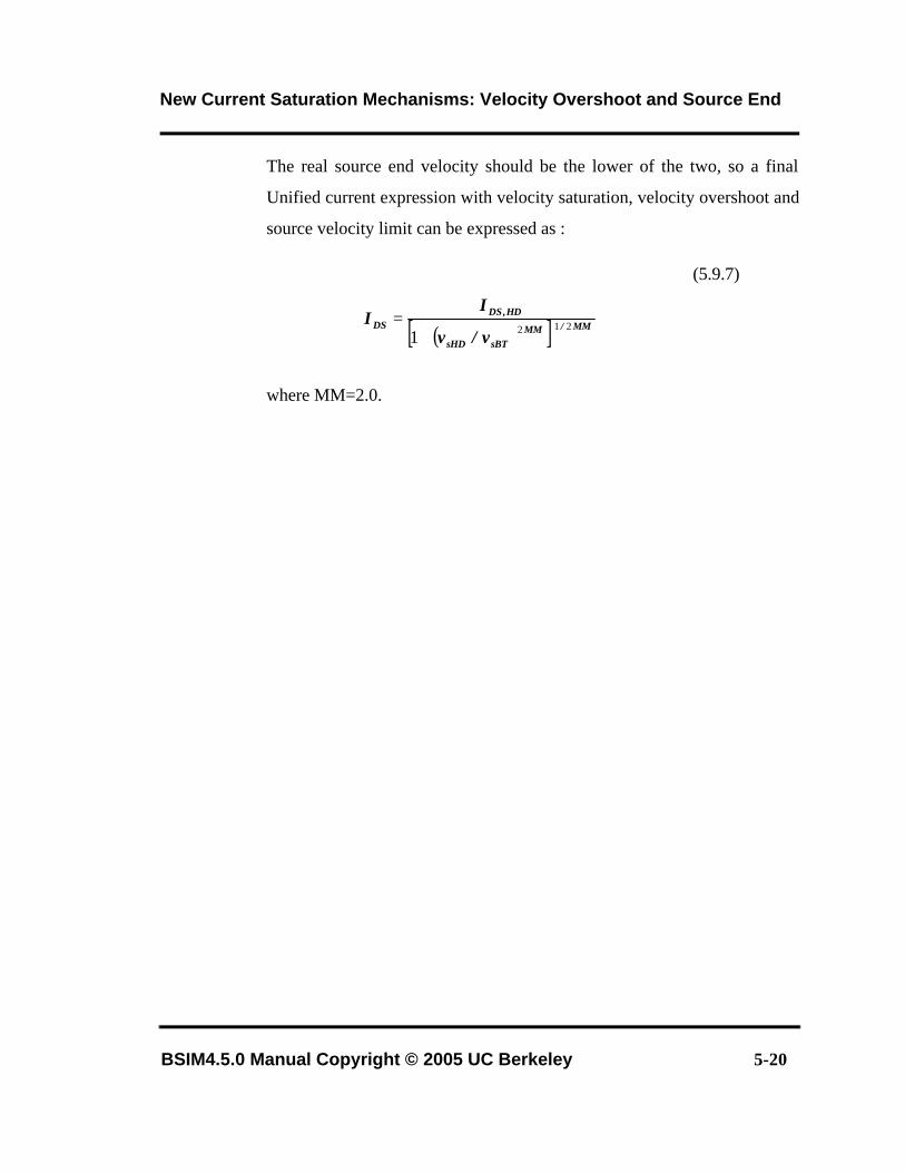
The real source end velocity should be the lower of the two, so a final
Unified current expression with velocity saturation, velocity overshoot and
source velocity limit can be expressed as :
(5.9.7)
where MM=2.0.
( )[ ] MM/MMsBTsHD
HD,DSDS
v/v
II 2121
+
=
BSIM4.3.0 Manual Copyright © 2003 UC Berkeley 6-1
Chapter 6: Body Current Models
In addition to the junction diode current and gate-to-body tunneling current, the substrate
terminal current consists of the substrate current due to impact ionization (Iii), and gate-
induced drain leakage current (IGIDL).
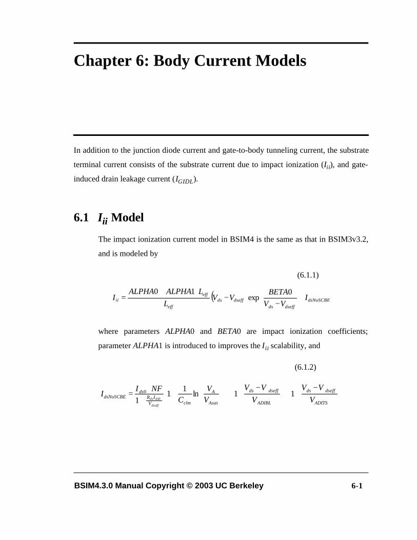
6.1 Iii Model
The impact ionization current model in BSIM4 is the same as that in BSIM3v3.2,
and is modeled by
(6.1.1)
where parameters ALPHA0 and BETA0 are impact ionization coefficients;
parameter ALPHA1 is introduced to improves the Iii scalability, and
(6.1.2)
( ) dsNoSCBEdseffds
dseffdseff
effii I
VVBETA
VVL
LALPHAALPHAI ⋅
−−
⋅+=
0exp
10
−+⋅
−+⋅
+
+⋅
=ADITS
dseffds
ADIBL
dseffds
Asat
A
clmVIR
dsdsNoSCBE V
VVV
VVVV
CNFI
Idseff
dsds11ln
11
1 0
0
IGIDL and IGISL Model
6-2 BSIM4.3.0 Manual Copyright © 2003 UC Berkeley
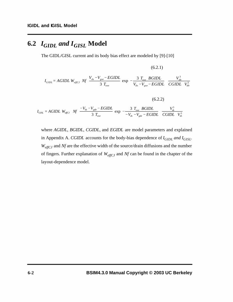
6.2 IGIDL and IGISL Model
The GIDL/GISL current and its body bias effect are modeled by [9]-[10]
(6.2.1)
(6.2.2)
where AGIDL, BGIDL, CGIDL, and EGIDL are model parameters and explained
in Appendix A. CGIDL accounts for the body-bias dependence of IGIDL and IGISL.
WeffCJ and Nf are the effective width of the source/drain diffusions and the number
of fingers. Further explanation of WeffCJ and Nf can be found in the chapter of the
layout-dependence model.
3
33exp
3 db
db
gseds
oxe
oxe
gsedseffCJGIDL VCGIDL
VEGIDLVV
BGIDLTT
EGIDLVVNfWAGIDLI
+⋅
−−⋅⋅−⋅
⋅
−−⋅⋅⋅=
3
33exp
3 sb
sb
gdeds
oxe
oxe
gdedseffCJGISL VCGIDL
VEGIDLVV
BGIDLTT
EGIDLVVNfWAGIDLI
+⋅
−−−⋅⋅
−⋅⋅
−−−⋅⋅⋅=
BSIM4.5.0 Manual Copyright © 2005 UC Berkeley 7-1
Chapter 7: Capacitance Model
Accurate modeling of MOSFET capacitance plays equally important role as that of the
DC model. This chapter describes the methodology and device physics considered in both
intrinsic and extrinsic capacitance modeling in BSIM4.0.0. Complete model parameters
can be found in Appendix A.
7.1 General Description
BSIM4.0.0 provides three options for selecting intrinsic and overlap/fringing
capacitance models. These capacitance models come from BSIM3v3.2, and the
BSIM3v3.2 capacitance model parameters are used without change in BSIM4.
except that separate CKAPPA parameters are introduced for the source-side and
drain-side overlap capacitances. The BSIM3v3.2 capMod = 1 is no longer
supported in BSIM4. The following table maps the BSIM4 capacitance models to
those of BSIM3v3.2.
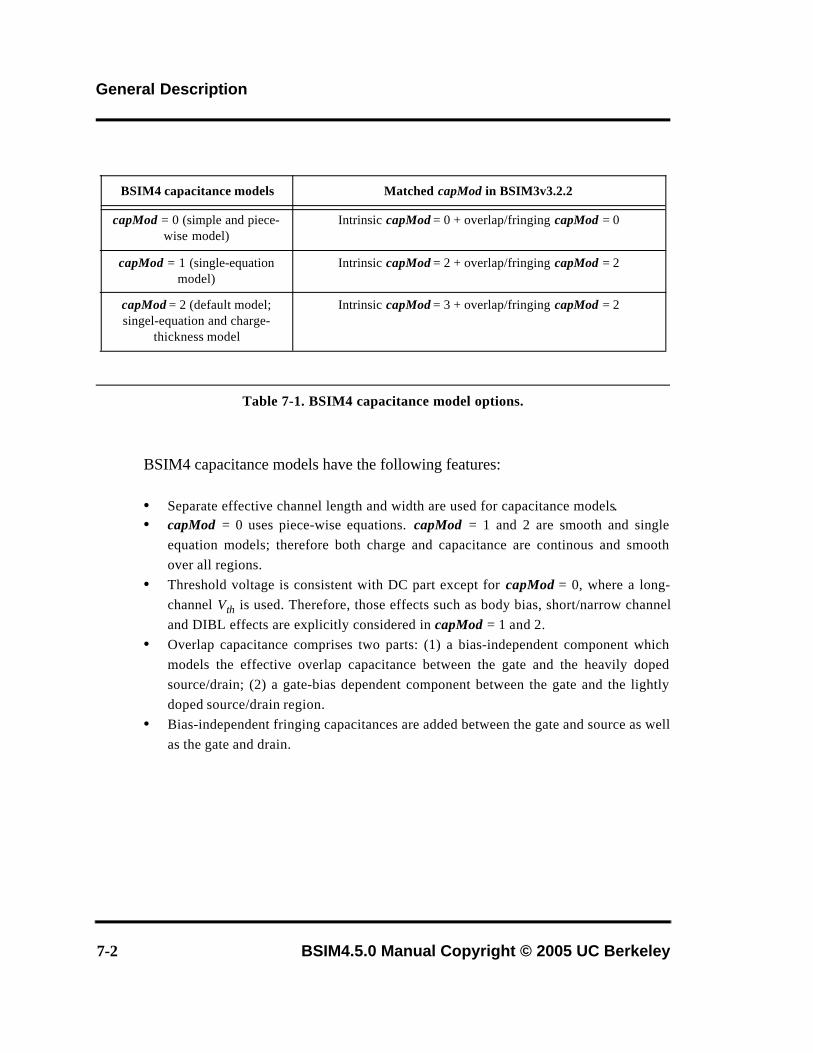
General Description
7-2 BSIM4.5.0 Manual Copyright © 2005 UC Berkeley
Table 7-1. BSIM4 capacitance model options.
BSIM4 capacitance models have the following features:
• Separate effective channel length and width are used for capacitance models.• capMod = 0 uses piece-wise equations. capMod = 1 and 2 are smooth and single
equation models; therefore both charge and capacitance are continous and smoothover all regions.
• Threshold voltage is consistent with DC part except for capMod = 0, where a long-channel Vth is used. Therefore, those effects such as body bias, short/narrow channeland DIBL effects are explicitly considered in capMod = 1 and 2.
• Overlap capacitance comprises two parts: (1) a bias-independent component whichmodels the effective overlap capacitance between the gate and the heavily dopedsource/drain; (2) a gate-bias dependent component between the gate and the lightlydoped source/drain region.
• Bias-independent fringing capacitances are added between the gate and source as wellas the gate and drain.
BSIM4 capacitance models Matched capMod in BSIM3v3.2.2
capMod = 0 (simple and piece- wise model)
Intrinsic capMod = 0 + overlap/fringing capMod = 0
capMod = 1 (single-equation model)
Intrinsic capMod = 2 + overlap/fringing capMod = 2
capMod = 2 (default model;singel-equation and charge-
thickness model
Intrinsic capMod = 3 + overlap/fringing capMod = 2
Methodology for Intrinsic Capacitance Modeling
BSIM4.5.0 Manual Copyright © 2005 UC Berkeley 7-3
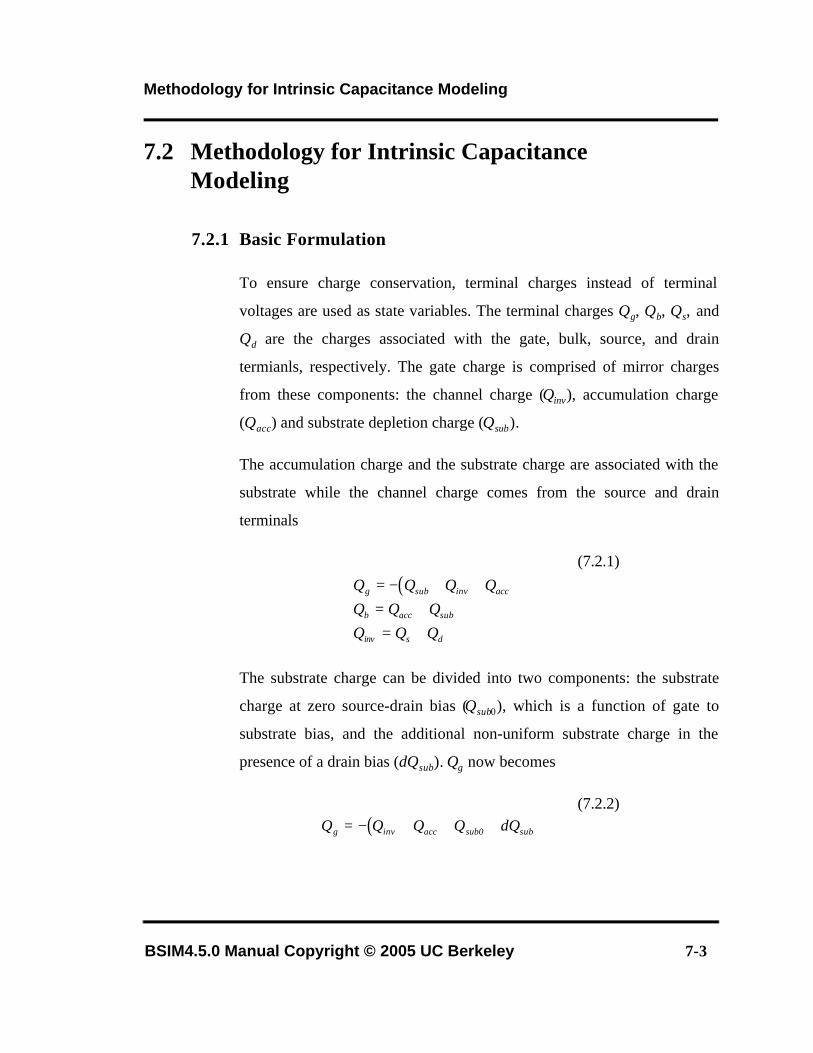
7.2 Methodology for Intrinsic Capacitance Modeling
7.2.1 Basic Formulation
To ensure charge conservation, terminal charges instead of terminal
voltages are used as state variables. The terminal charges Qg, Qb, Qs, and
Qd are the charges associated with the gate, bulk, source, and drain
termianls, respectively. The gate charge is comprised of mirror charges
from these components: the channel charge (Qinv), accumulation charge
(Qacc) and substrate depletion charge (Qsub).
The accumulation charge and the substrate charge are associated with the
substrate while the channel charge comes from the source and drain
terminals
(7.2.1)
The substrate charge can be divided into two components: the substrate
charge at zero source-drain bias (Qsub0), which is a function of gate to
substrate bias, and the additional non-uniform substrate charge in the
presence of a drain bias (δQsub). Qg now becomes
(7.2.2)
( )Q Q Q QQ Q QQ Q Q
g sub inv acc
b acc sub
inv s d
= − + += += +
( )Q Q Q Q Qg inv acc sub sub= − + + +0 δ
Methodology for Intrinsic Capacitance Modeling
7-4 BSIM4.5.0 Manual Copyright © 2005 UC Berkeley
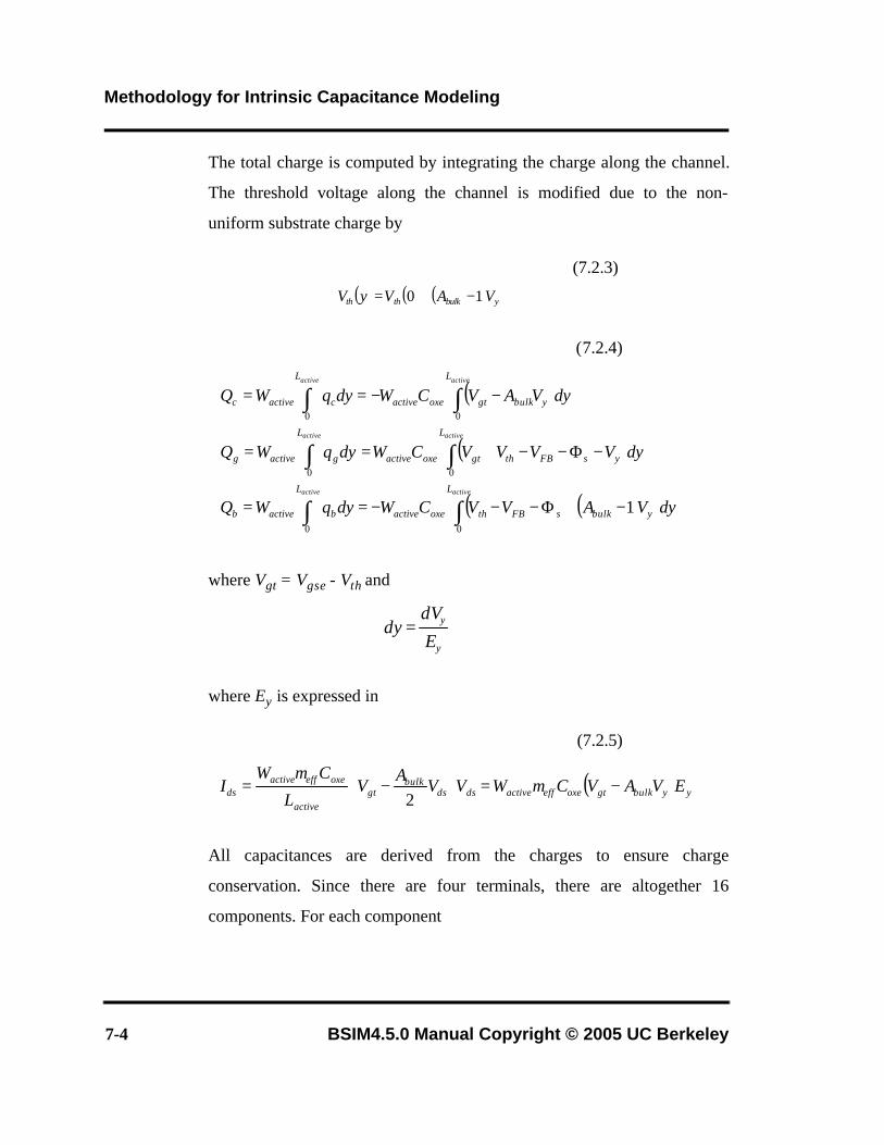
The total charge is computed by integrating the charge along the channel.
The threshold voltage along the channel is modified due to the non-
uniform substrate charge by
(7.2.3)
(7.2.4)
where Vgt = Vgse - Vth and
where Ey is expressed in
(7.2.5)
All capacitances are derived from the charges to ensure charge
conservation. Since there are four terminals, there are altogether 16
components. For each component
( ) ( ) ( ) ybulkthth VAVyV 10 −+=
( )
( )
( )( )
−+Φ−−−==
−Φ−−+==
−−==
∫ ∫
∫ ∫
∫ ∫
active active
active active
active active
L L
ybulksFBthoxeactivebactiveb
L L
ysFBthgtoxeactivegactiveg
L L
ybulkgtoxeactivecactivec
dyVAVVCWdyqWQ
dyVVVVCWdyqWQ
dyVAVCWdyqWQ
0 0
0 0
0 0
1
y
y
E
dVdy =
( ) yybulkgtoxeeffactivedsdsbulk
gtactive
oxeeffactiveds EVAVCWVV
AV
L
CWI −=
−= µ
µ
2
Methodology for Intrinsic Capacitance Modeling
BSIM4.5.0 Manual Copyright © 2005 UC Berkeley 7-5
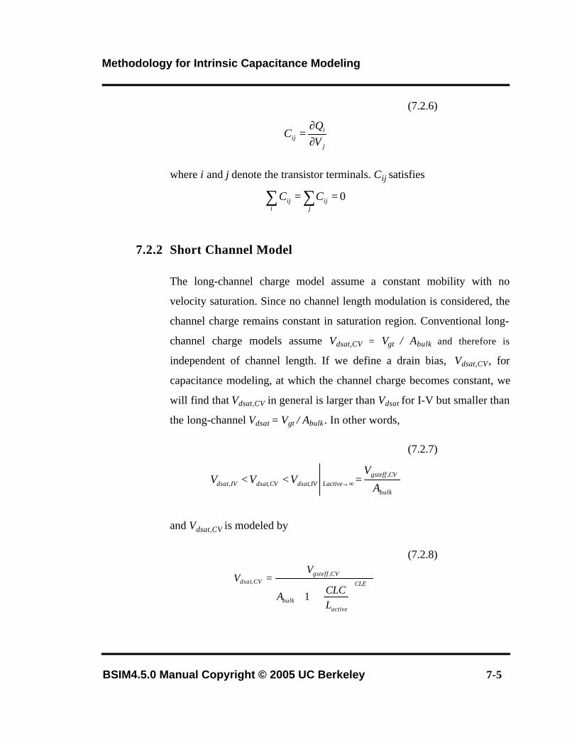
(7.2.6)
where i and j denote the transistor terminals. Cij satisfies
7.2.2 Short Channel Model
The long-channel charge model assume a constant mobility with no
velocity saturation. Since no channel length modulation is considered, the
channel charge remains constant in saturation region. Conventional long-
channel charge models assume Vdsat,CV = Vgt / Abulk and therefore is
independent of channel length. If we define a drain bias, Vdsat,CV , for
capacitance modeling, at which the channel charge becomes constant, we
will find that Vdsat,CV in general is larger than Vdsat for I-V but smaller than
the long-channel Vdsat = Vgt / Abulk . In other words,
(7.2.7)
and Vdsat,CV is modeled by
(7.2.8)
j
iij V
QC
∂∂
=
∑∑ ==j
iji
ij CC 0
bulk
CVgsteffLactiveIVdsatCVdsatIVdsat A
VVVV ,
,,, =<< ∞→
+⋅
=CLE
activebulk
CVgsteffCVdsat
LCLCA
VV
1
,,
Methodology for Intrinsic Capacitance Modeling
7-6 BSIM4.5.0 Manual Copyright © 2005 UC Berkeley
(7.2.9)
Model parameters CLC and CLE are introduced to consider the effect of
channel-length modulation. Abulk for the capacitance model is modeled by
(7.2.10)
where
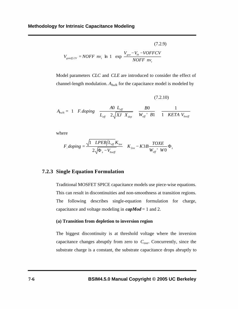
7.2.3 Single Equation Formulation
Traditional MOSFET SPICE capacitance models use piece-wise equations.
This can result in discontinuities and non-smoothness at transition regions.
The following describes single-equation formulation for charge,
capacitance and voltage modeling in capMod = 1 and 2.
(a) Transition from depletion to inversion region
The biggest discontinuity is at threshold voltage where the inversion
capacitance changes abruptly from zero to Coxe. Concurrently, since the
substrate charge is a constant, the substrate capacitance drops abruptly to
⋅
−−+⋅⋅=
t
thgsetCVgsteff nvNOFF
VOFFCVVVnvNOFFV exp1ln,
bseffeffdepeff
effbulk VKETABW
BXXJL
LAdopingFA
⋅+
⋅
++⋅
⋅+
⋅⋅+= − 1
11'
02
01
seff
oxbseffs
oxeff
WWTOXE
BKKV
KLLPEBdopingF Φ
+−+
−Φ
+=− 0'
32
12
1
Methodology for Intrinsic Capacitance Modeling
BSIM4.5.0 Manual Copyright © 2005 UC Berkeley 7-7
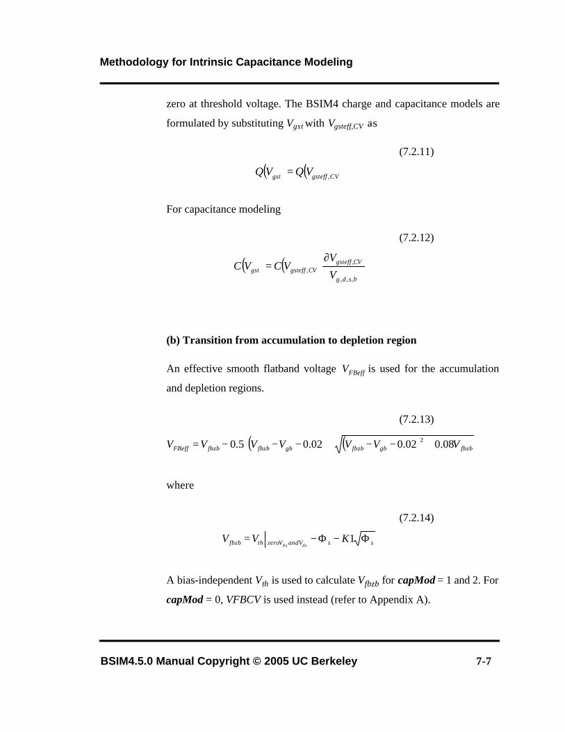
zero at threshold voltage. The BSIM4 charge and capacitance models are
formulated by substituting Vgst with Vgsteff,CV as
(7.2.11)
For capacitance modeling
(7.2.12)
(b) Transition from accumulation to depletion region
An effective smooth flatband voltage VFBeff is used for the accumulation
and depletion regions.
(7.2.13)
where
(7.2.14)
A bias-independent Vth is used to calculate Vfbzb for capMod = 1 and 2. For
capMod = 0, VFBCV is used instead (refer to Appendix A).
( ) ( )CVgsteffgst VQVQ ,=
( ) ( )bsdg
CVgsteffCVgsteffgst V
VVCVC
,,,
,,
∂=
( ) ( )
+−−+−−−= fbzbgbfbzbgbfbzbfbzbFBeff VVVVVVV 08.002.002.05.0 2
ssVandVzerothfbzb KVVdsbs
Φ−Φ−= 1
Methodology for Intrinsic Capacitance Modeling
7-8 BSIM4.5.0 Manual Copyright © 2005 UC Berkeley
(c) Transition from linear to saturation region
An effective Vds, Vcveff, is used to smooth out the transition between linear
and saturation regions.
(7.2.15)
7.2.4 Charge partitioning
The inversion charges are partitioned into Qinv = Qs + Qd. The ratio of Qd to
Qs is the charge partitioning ratio. Existing charge partitioning schemes are
0/100, 50/50 and 40/60 (XPART = 1, 0.5 and 0).
50/50 charge partition
This is the simplest of all partitioning schemes in which the inversion
charges are assumed to be contributed equally from the source and drain
terminals.
40/60 charge partition
This is the most physical model of the three partitioning schemes in which
the channel charges are allocated to the source and drain terminals by
assuming a linear dependence on channel position y.
{ } VVVVwhereVVVVV dsCVdsatCVdsatCVdsatcveff 02.0;45.0 44,4,42
44, =−−=++−= δδδ
Charge-Thickness Capacitance Model (CTM)
BSIM4.5.0 Manual Copyright © 2005 UC Berkeley 7-9
(7.2.16)
0/100 charge partition
In fast transient simulations, the use of a quasi-static model may result in a
large unrealistic drain current spike. This partitioning scheme is developed
to artificially suppress the drain current spike by assigning all inversion
charges in the saturation region to the source electrode. Notice that this
charge partitioning scheme will still give drain current spikes in the linear
region and aggravate the source current spike problem.
7.3 Charge-Thickness Capacitance Model (CTM)
Current MOSFET models in SPICE generally overestimate the intrinsic
capacitance and usually are not smooth at Vfb and Vth. The discrepancy is more
pronounced in thinner Tox devices due to the assumption of inversion and
accumulation charge being located at the interface. Numerical quantum simulation
results in Figure 7-1 indicate the significant charge thickness in all regions of
operation.
Q W q yL
dy
Q W qy
Ldy
s active cactive
L
d active cactive
L
active
active
= −
=
∫
∫
10
0
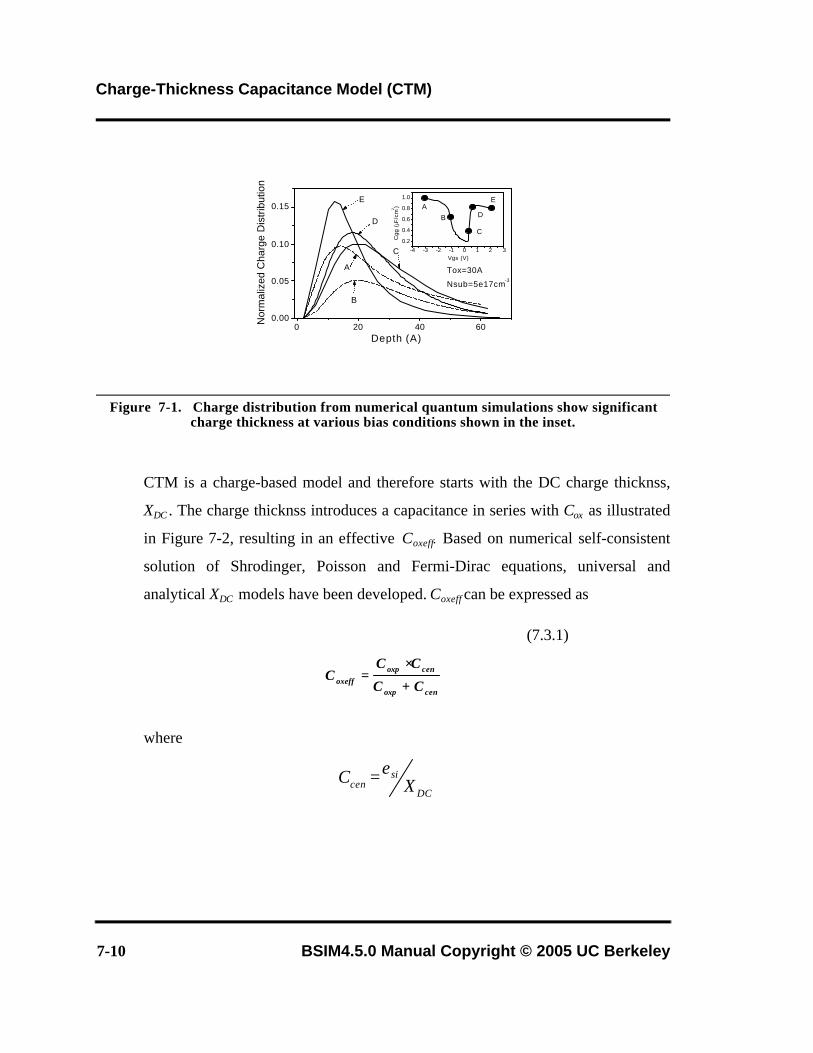
Charge-Thickness Capacitance Model (CTM)
7-10 BSIM4.5.0 Manual Copyright © 2005 UC Berkeley
Figure 7-1. Charge distribution from numerical quantum simulations show significant charge thickness at various bias conditions shown in the inset.
CTM is a charge-based model and therefore starts with the DC charge thicknss,
XDC . The charge thicknss introduces a capacitance in series with Cox as illustrated
in Figure 7-2, resulting in an effective Coxeff. Based on numerical self-consistent
solution of Shrodinger, Poisson and Fermi-Dirac equations, universal and
analytical XDC models have been developed. Coxeff can be expressed as
(7.3.1)
where
0 20 40 600.00
0.05
0.10
0.15
Tox=30A
Nsub=5e17cm-3
C
D
A
B
E
Nor
mal
ized
Cha
rge
Dis
trib
utio
n
Depth (A)
-4 -3 -2 -1 0 1 2 3
0.2
0.4
0.6
0.8
1.0 E
D
C
B
A
Cgg
(µF
/cm
2 )
Vgs (V)
cenoxp
cenoxpoxeff CC
CCC
+
⋅=
DC
sicen XC ε=
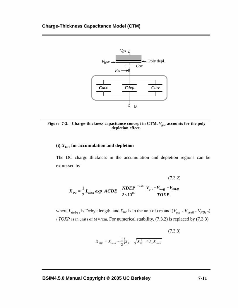
Charge-Thickness Capacitance Model (CTM)
BSIM4.5.0 Manual Copyright © 2005 UC Berkeley 7-11
Figure 7-2. Charge-thickness capacitance concept in CTM. Vgse accounts for the poly depletion effect.
(i) XDC for accumulation and depletion
The DC charge thickness in the accumulation and depletion regions can be
expressed by
(7.3.2)
where Ldebye is Debye length, and XDC is in the unit of cm and (Vgse - Vbseff - VFBeff)
/ TOXP is in units of MV/cm. For numerical statbility, (7.3.2) is replaced by (7.3.3)
(7.3.3)
CoxPoly depl.
Cacc Cdep Cinv
B
Vgs
Vgse
Φs
−−⋅
×⋅=
−
TOXP
VVVNDEPACDEexpLX FBeffbseffgse
.
debyeDC
250
1610231
( )max2
00max 421 XXXXX xDC δ++−=
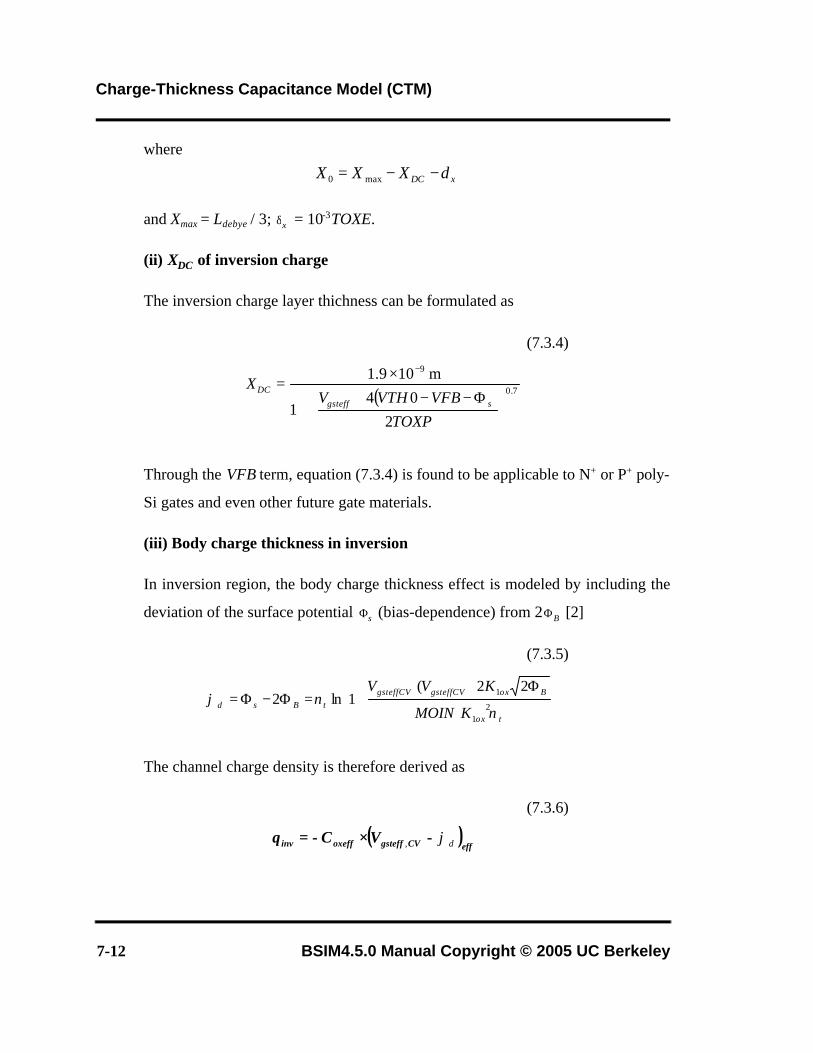
Charge-Thickness Capacitance Model (CTM)
7-12 BSIM4.5.0 Manual Copyright © 2005 UC Berkeley
where
and Xmax = Ldebye / 3; = 10-3TOXE.
(ii) XDC of inversion charge
The inversion charge layer thichness can be formulated as
(7.3.4)
Through the VFB term, equation (7.3.4) is found to be applicable to N+ or P+ poly-
Si gates and even other future gate materials.
(iii) Body charge thickness in inversion
In inversion region, the body charge thickness effect is modeled by including the
deviation of the surface potential (bias-dependence) from 2 [2]
(7.3.5)
The channel charge density is therefore derived as
(7.3.6)
xDCXXX δ−−= max0
δx
( ) 7.0
9
204
1
m109.1
Φ−−++
×=
−
TOXPVFBVTHV
Xsgsteff
DC
Φs ΦB
⋅
Φ+⋅+=Φ−Φ=
tox
BoxgsteffCVgsteffCVtBs
KMOIN
KVV
ννϕδ 2
1
1 22(1ln2
( )effCVgsteffoxeffinv VCq δϕ−⋅−= ,
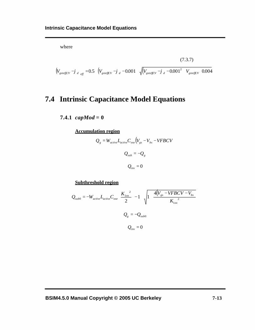
Intrinsic Capacitance Model Equations
BSIM4.5.0 Manual Copyright © 2005 UC Berkeley 7-13
where
(7.3.7)
7.4 Intrinsic Capacitance Model Equations
7.4.1 capMod = 0
Accumulation region
Subthreshold region
( ) ( ) ( )
⋅+−−+−−⋅=− 004.0001.0001.05.0 ,
2,,, CVgsteffCVgsteffCVgsteffeffCVgsteff VVVV δδδ ϕϕϕ
( )VFBCVVVCLWQ bsgsoxeactiveactiveg −−=
gsub QQ −=
0=invQ
( )
−−++−⋅−= 2
1
21
0
411
2 ox
bsgsoxoxeactiveactivesub K
VVFBCVVKCLWQ
0subg QQ −=
0=invQ
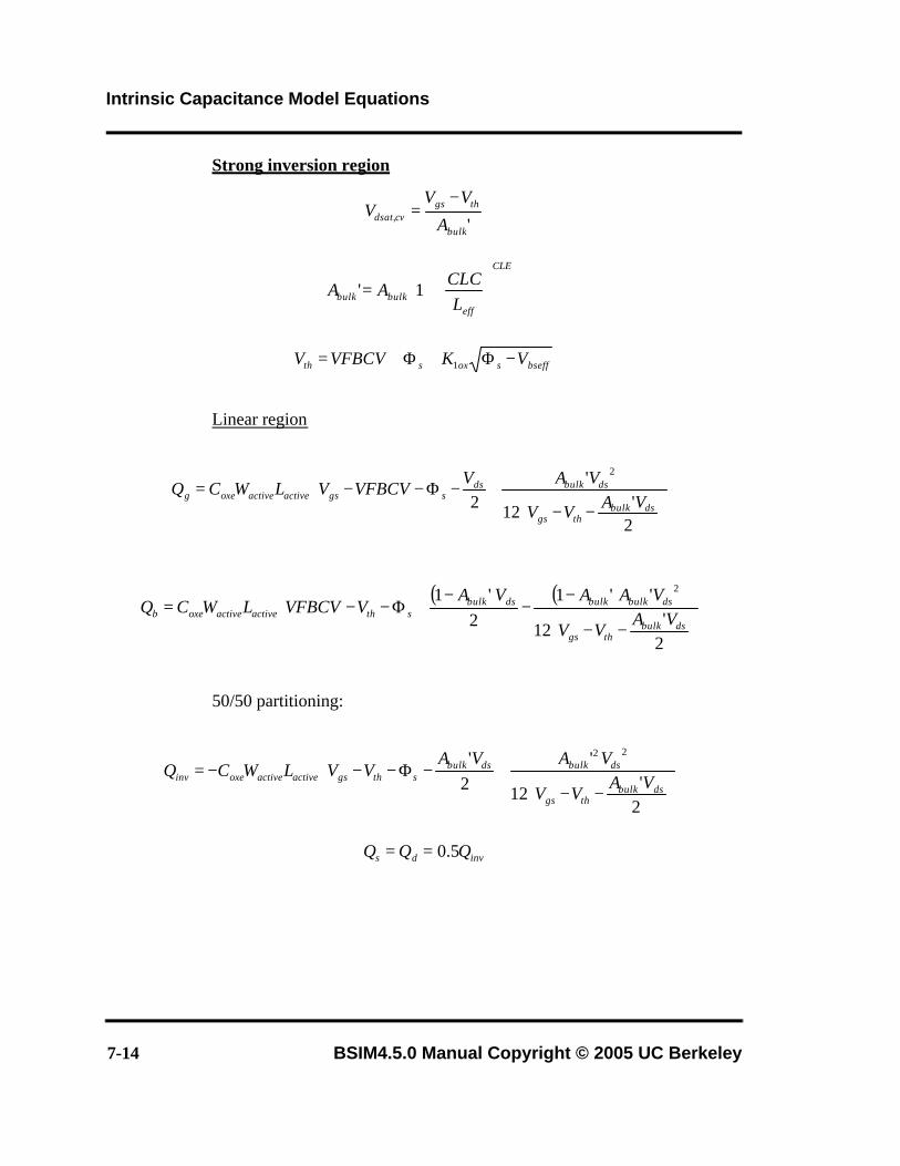
Intrinsic Capacitance Model Equations
7-14 BSIM4.5.0 Manual Copyright © 2005 UC Berkeley
Strong inversion region
Linear region
50/50 partitioning:
',bulk
thgscvdsat A
VVV
−=
+=
CLE
effbulkbulk L
CLCAA 1'
bseffsoxsth VKVFBCVV −Φ+Φ+= 1
−−
+−Φ−−=
2'12
'2
2
dsbulkthgs
dsbulkdssgsactiveactiveoxeg VAVV
VAVVFBCVVLWCQ
( ) ( )
−−
−−
−+Φ−−=
2'
12
''12
'1 2
dsbulkthgs
dsbulkbulkdsbulksthactiveactiveoxeb VA
VV
VAAVAVVFBCVLWCQ
−−
+−Φ−−−=
2'
12
'2' 22
dsbulkthgs
dsbulkdsbulksthgsactiveactiveoxeinv VA
VV
VAVAVVLWCQ
invds QQQ 5.0==
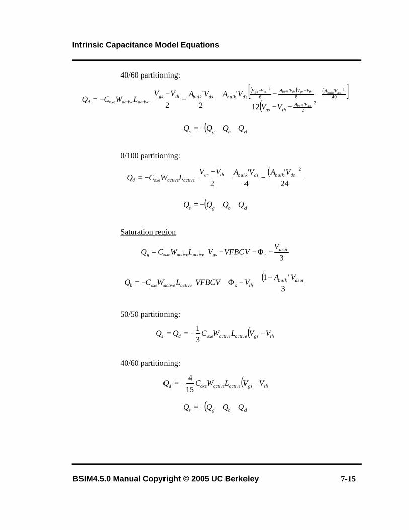
Intrinsic Capacitance Model Equations
BSIM4.5.0 Manual Copyright © 2005 UC Berkeley 7-15
40/60 partitioning:
0/100 partitioning:
Saturation region
50/50 partitioning:
40/60 partitioning:
( ) ( ) ( )[ ]( )
−−
+−+−
−−=
−−
2
2'
40'
8'
6
12
'2'
2
22
dsbulk
dsbulkthgsdsbulkthgs
VAthgs
VAVVVAVVdsbulkdsbulkthgs
activeactiveoxedVV
VAVAVVLWCQ
( )dbgs QQQQ ++−=
( )
−+
−−=
24'
4'
2
2dsbulkdsbulkthgs
activeactiveoxedVAVAVV
LWCQ
( )dbgs QQQQ ++−=
−Φ−−=
3dsat
sgsactiveactiveoxegV
VFBCVVLWCQ
( )
−
+−Φ+−=3
'1 dsatbulkthsactiveactiveoxeb
VAVVFBCVLWCQ
( )thgsactiveactiveoxeds VVLWCQQ −−==31
( )thgsactiveactiveoxed VVLWCQ −−=154
( )dbgs QQQQ ++−=
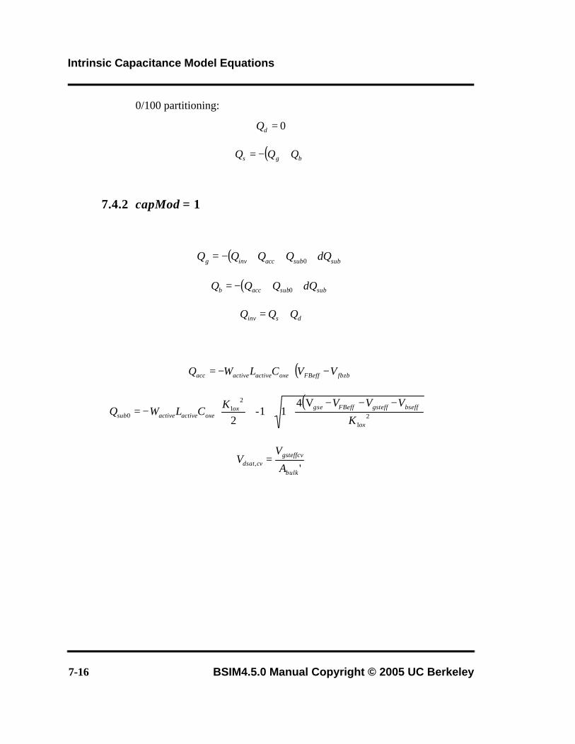
Intrinsic Capacitance Model Equations
7-16 BSIM4.5.0 Manual Copyright © 2005 UC Berkeley
0/100 partitioning:
7.4.2 capMod = 1
0=dQ
( )bgs QQQ +−=
( )subsubaccinvg QQQQQ δ+++−= 0
( )subsubaccb QQQQ δ++−= 0
dsinv QQQ +=
( )fbzbFBeffoxeactiveactiveacc VVCLWQ −⋅−=
( )
−−−++⋅⋅−=
V411-
2 21
21
0ox
bseffgsteffFBeffgseoxoxeactiveactivesub K
VVVKCLWQ
',bulk
gsteffcvcvdsat A
VV =
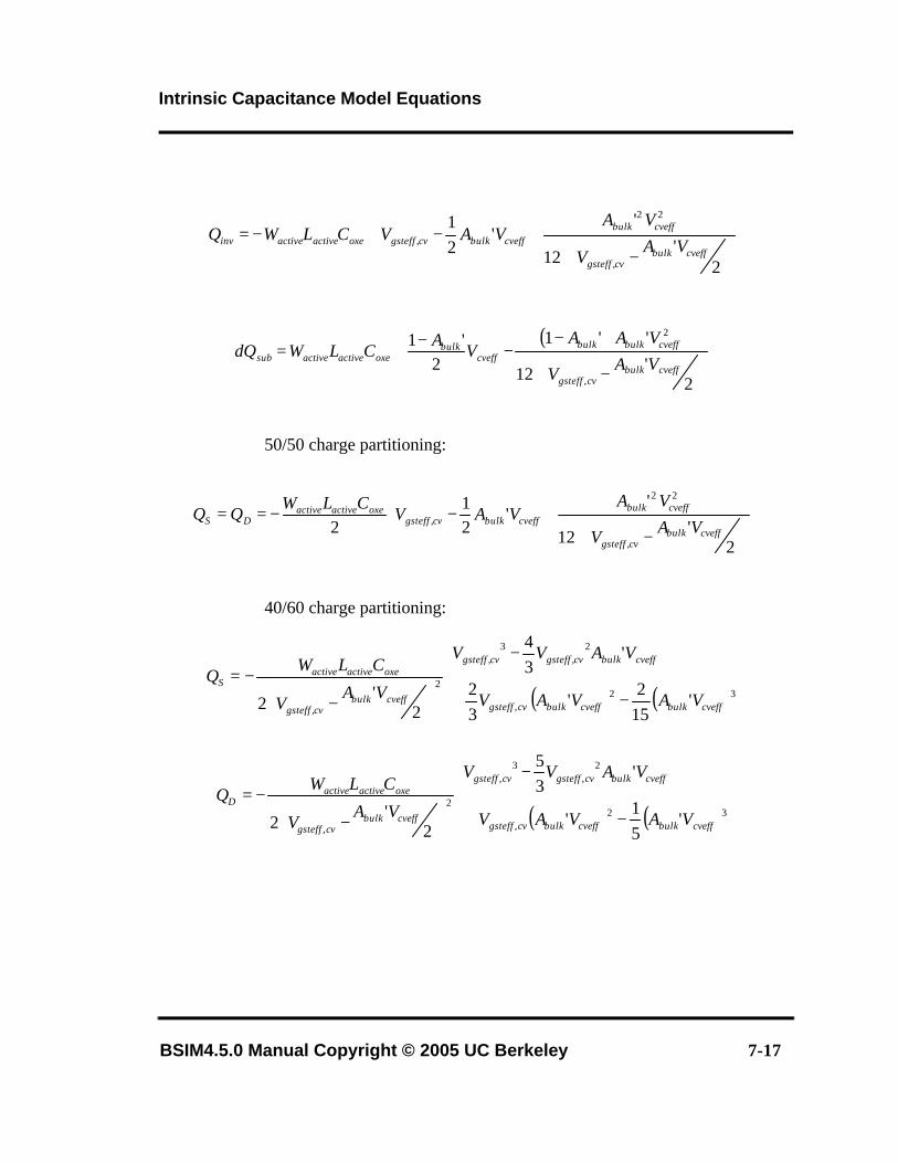
Intrinsic Capacitance Model Equations
BSIM4.5.0 Manual Copyright © 2005 UC Berkeley 7-17
50/50 charge partitioning:
40/60 charge partitioning:
−⋅
+−⋅−=
2'
12
''
21
,
22
,cveffbulk
cvgsteff
cveffbulkcveffbulkcvgsteffoxeactiveactiveinv VA
V
VAVAVCLWQ
( )
−⋅
⋅−−
−⋅=
2'12
''12
'1
,
2
cveffbulkcvgsteff
cveffbulkbulkcveff
bulkoxeactiveactivesub VAV
VAAV
ACLWQδ
−⋅
+−−==
2'12
''
21
2,
22
,cveffbulk
cvgsteff
cveffbulkcveffbulkcvgsteff
oxeactiveactiveDS VAV
VAVAV
CLWQQ
( ) ( )
−+
−
−
−=32
,
2,
3,
2
,'
152
'32
'34
2'
2 cveffbulkcveffbulkcvgsteff
cveffbulkcvgsteffcvgsteff
cveffbulkcvgsteff
oxeactiveactiveS
VAVAV
VAVV
VAV
CLWQ
( ) ( )
−+
−
−
−=32
,
2,
3,
2
,'
51
'
'35
2'
2 cveffbulkcveffbulkcvgsteff
cveffbulkcvgsteffcvgsteff
cveffbulkcvgsteff
oxeactiveactiveD
VAVAV
VAVV
VAV
CLWQ
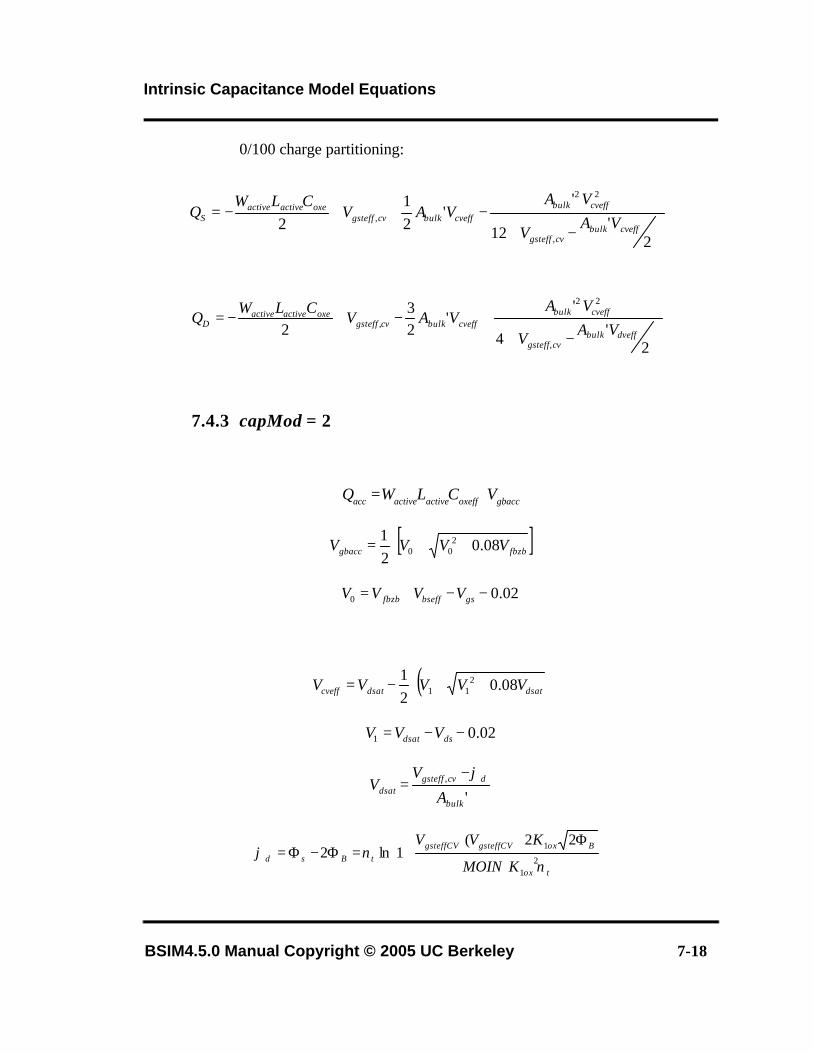
Intrinsic Capacitance Model Equations
BSIM4.5.0 Manual Copyright © 2005 UC Berkeley 7-18
0/100 charge partitioning:
7.4.3 capMod = 2
−⋅
−+⋅−=
2'
12
''
21
2,
22
,cveffbulk
cvgsteff
cveffbulkcveffbulkcvgsteff
oxeactiveactiveS VA
V
VAVAV
CLWQ
−⋅
+−⋅−=
2'4
''
23
2,
22
,dveffbulk
cvgsteff
cveffbulkcveffbulkcvgsteff
oxeactiveactiveD VAV
VAVAV
CLWQ
gbaccoxeffactiveactiveacc VCLWQ ⋅=
[ ]fbzbgbacc VVVV 08.021 2
00 ++⋅=
02.00 −−+= gsbsefffbzb VVVV
( )dsatdsatcveff VVVVV 08.021 2
11 ++⋅−=
02.01 −−= dsdsat VVV
',
bulk
cvgsteffdsat A
VV δϕ−
=
⋅
Φ+⋅+=Φ−Φ=
tox
BoxgsteffCVgsteffCVtBs
KMOIN
KVV
ννϕδ 2
1
1 22(1ln2
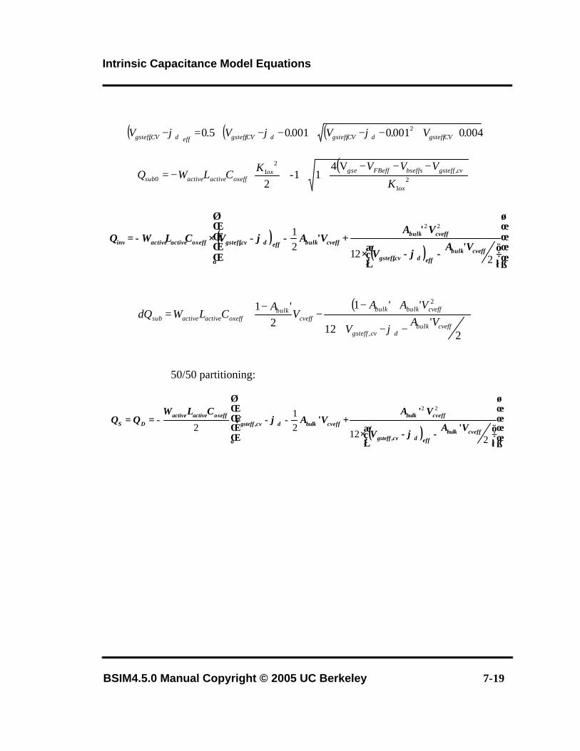
Intrinsic Capacitance Model Equations
BSIM4.5.0 Manual Copyright © 2005 UC Berkeley 7-19
50/50 partitioning:
( ) ( ) ( )
⋅+−−+−−⋅=− 004.0001.0001.05.0 ,
2,,, CVgsteffCVgsteffCVgsteffeffCVgsteff VVVV δδδ ϕϕϕ
( )
−−−++⋅⋅−=
V411-
2 21
,2
10
ox
cvgsteffbseffsFBeffgseoxoxeffactiveactivesub K
VVVKCLWQ
( )( )
−−⋅
+−−⋅−=
21221
22
cveffbulkeffcvgsteff
cveffbulkcveffbulkeffcvgsteffoxeffactiveactiveinv VA
V
VAVAVCLWQ
'
''
,
,
δ
δ
ϕϕ
( )
−−⋅
⋅−−
−⋅=
2'
12
''1
2'1
,
2
cveffbulkcvgsteff
cveffbulkbulkcveff
bulkoxeffactiveactivesub VA
V
VAAV
ACLWQ
δϕδ
( )
−−⋅
+−−−==
21221
2
22
cveffbulkeffcvgsteff
cveffbulkcveffbulkcvgsteff
oxeffactiveactiveDS VA
V
VAVAV
CLWQQ
'
''
,
,
δ
δ
ϕϕ
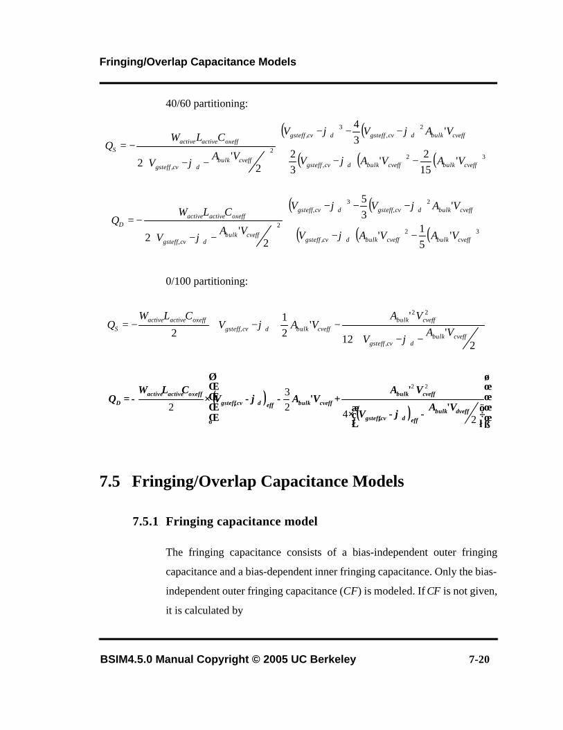
Fringing/Overlap Capacitance Models
BSIM4.5.0 Manual Copyright © 2005 UC Berkeley 7-20
40/60 partitioning:
0/100 partitioning:
7.5 Fringing/Overlap Capacitance Models
7.5.1 Fringing capacitance model
The fringing capacitance consists of a bias-independent outer fringing
capacitance and a bias-dependent inner fringing capacitance. Only the bias-
independent outer fringing capacitance (CF) is modeled. If CF is not given,
it is calculated by
( ) ( )
( )( ) ( )
−−+
−−−
−−
−=32
,
2,
3,
2
,'
152
'32
'34
2'
2 cveffbulkcveffbulkcvgsteff
cveffbulkcvgsteffcvgsteff
cveffbulkcvgsteff
oxeffactiveactiveS
VAVAV
VAVV
VAV
CLWQ
δ
δδ
δϕ
ϕϕ
ϕ
( ) ( )
( )( ) ( )
−−+
−−−
−−
−=32
,
2,
3,
2
,'
51
'
'35
2'
2 cveffbulkcveffbulkcvgsteff
cveffbulkcvgsteffcvgsteff
cveffbulkcvgsteff
oxeffactiveactiveD
VAVAV
VAVV
VAV
CLWQ
δ
δδ
δϕ
ϕϕ
ϕ
−−⋅
−+−⋅−=
2'
12
''
21
2,
22
,cveffbulk
cvgsteff
cveffbulkcveffbulkcvgsteff
oxeffactiveactiveS VA
V
VAVAV
CLWQ
δ
δ
ϕϕ
( )( )
−−⋅
+−−⋅−=
2423
2
22
dveffbulkeffcvgsteff
cveffbulkcveffbulkeffcvgsteff
oxeffactiveactiveD VA
V
VAVAV
CLWQ
'
''
,
,
δ
δ
ϕϕ
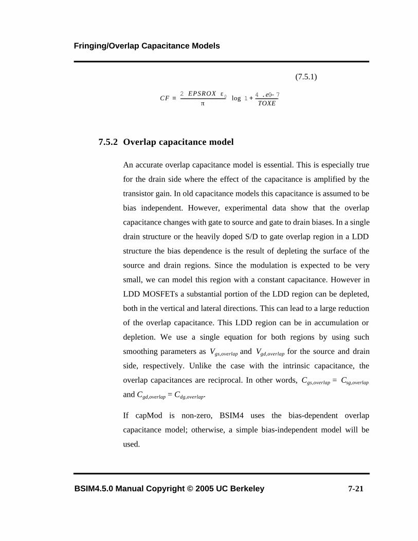
Fringing/Overlap Capacitance Models
BSIM4.5.0 Manual Copyright © 2005 UC Berkeley 7-21
(7.5.1)
7.5.2 Overlap capacitance model
An accurate overlap capacitance model is essential. This is especially true
for the drain side where the effect of the capacitance is amplified by the
transistor gain. In old capacitance models this capacitance is assumed to be
bias independent. However, experimental data show that the overlap
capacitance changes with gate to source and gate to drain biases. In a single
drain structure or the heavily doped S/D to gate overlap region in a LDD
structure the bias dependence is the result of depleting the surface of the
source and drain regions. Since the modulation is expected to be very
small, we can model this region with a constant capacitance. However in
LDD MOSFETs a substantial portion of the LDD region can be depleted,
both in the vertical and lateral directions. This can lead to a large reduction
of the overlap capacitance. This LDD region can be in accumulation or
depletion. We use a single equation for both regions by using such
smoothing parameters as Vgs,overlap and Vgd,overlap for the source and drain
side, respectively. Unlike the case with the intrinsic capacitance, the
overlap capacitances are reciprocal. In other words, Cgs,overlap = Csg,overlap
and Cgd,overlap = Cdg,overlap.
If capMod is non-zero, BSIM4 uses the bias-dependent overlap
capacitance model; otherwise, a simple bias-independent model will be
used.
CF2 EPSROX ε0⋅ ⋅
π---------------------------------------- 1 4.0 e 7–
TOXE---------------------+
log⋅=
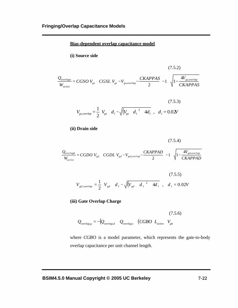
Fringing/Overlap Capacitance Models
BSIM4.5.0 Manual Copyright © 2005 UC Berkeley 7-22
Bias-dependent overlap capacitance model
(i) Source side
(7.5.2)
(7.5.3)
(ii) Drain side
(7.5.4)
(7.5.5)
(iii) Gate Overlap Charge
(7.5.6)
where CGBO is a model parameter, which represents the gate-to-body
overlap capacitance per unit channel length.
−+−−−+⋅=
CKAPPASVCKAPPAS
VVCGSLVCGSOW
Q overlapgsoverlapgsgsgs
active
soverlap ,,
, 411
2
( ) VVVV gsgsoverlapgs 02.0,421
112
11, =
++−+= δδδδ
−+−−−+⋅=
CKAPPADVCKAPPAD
VVCGDLVCGDOW
Q overlapgdoverlapgdgdgd
active
doverlap ,,
, 411
2
( ) VVVV gdgdoverlapgd 02.0,421
112
11, =
++−+= δδδδ
( )( )gbactivesoverlapdoverlapgoverlap VLCGBOQQQ ⋅⋅++−= ,,,
Fringing/Overlap Capacitance Models
BSIM4.5.0 Manual Copyright © 2005 UC Berkeley 7-23
Bias-independent overlap capacitance model
If capMod = 0, a bias-independent overlap capacitance model will be used.
In this case, model parameters CGSL, CGDL, CKAPPAS and CKAPPD all
have no effect.
The gate-to-source overlap charge is expressed by
The gate-to-drain overlap charge is calculated by
The gate-to-substrate overlap charge is computed by
Default CGSO and CGDO
If CGSO and CGDO (the overlap capacitances between the gate and the
heavily doped source/drain regions, respectively) are not given, they will
be calculated. Appendix A gives the information on how CGSO, CGDO
and CGBO are calculated.
gsactivesoverlap VCGSOWQ ⋅⋅=,
gdactivedoverlap VCGDOWQ ⋅⋅=,
gbactiveboverlap VCGBOLQ ⋅⋅=,
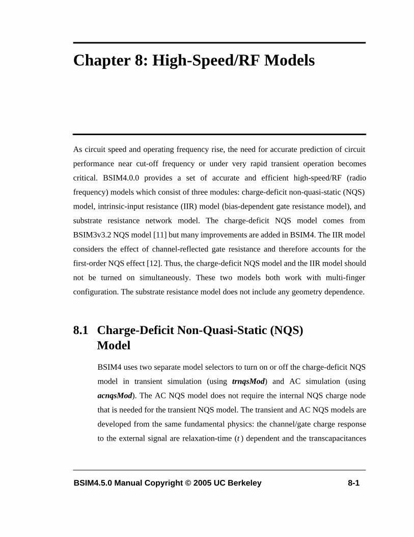
BSIM4.5.0 Manual Copyright © 2005 UC Berkeley 8-1
Chapter 8: High-Speed/RF Models
As circuit speed and operating frequency rise, the need for accurate prediction of circuit
performance near cut-off frequency or under very rapid transient operation becomes
critical. BSIM4.0.0 provides a set of accurate and efficient high-speed/RF (radio
frequency) models which consist of three modules: charge-deficit non-quasi-static (NQS)
model, intrinsic-input resistance (IIR) model (bias-dependent gate resistance model), and
substrate resistance network model. The charge-deficit NQS model comes from
BSIM3v3.2 NQS model [11] but many improvements are added in BSIM4. The IIR model
considers the effect of channel-reflected gate resistance and therefore accounts for the
first-order NQS effect [12]. Thus, the charge-deficit NQS model and the IIR model should
not be turned on simultaneously. These two models both work with multi-finger
configuration. The substrate resistance model does not include any geometry dependence.
8.1 Charge-Deficit Non-Quasi-Static (NQS) Model
BSIM4 uses two separate model selectors to turn on or off the charge-deficit NQS
model in transient simulation (using trnqsMod) and AC simulation (using
acnqsMod). The AC NQS model does not require the internal NQS charge node
that is needed for the transient NQS model. The transient and AC NQS models are
developed from the same fundamental physics: the channel/gate charge response
to the external signal are relaxation-time (τ) dependent and the transcapacitances
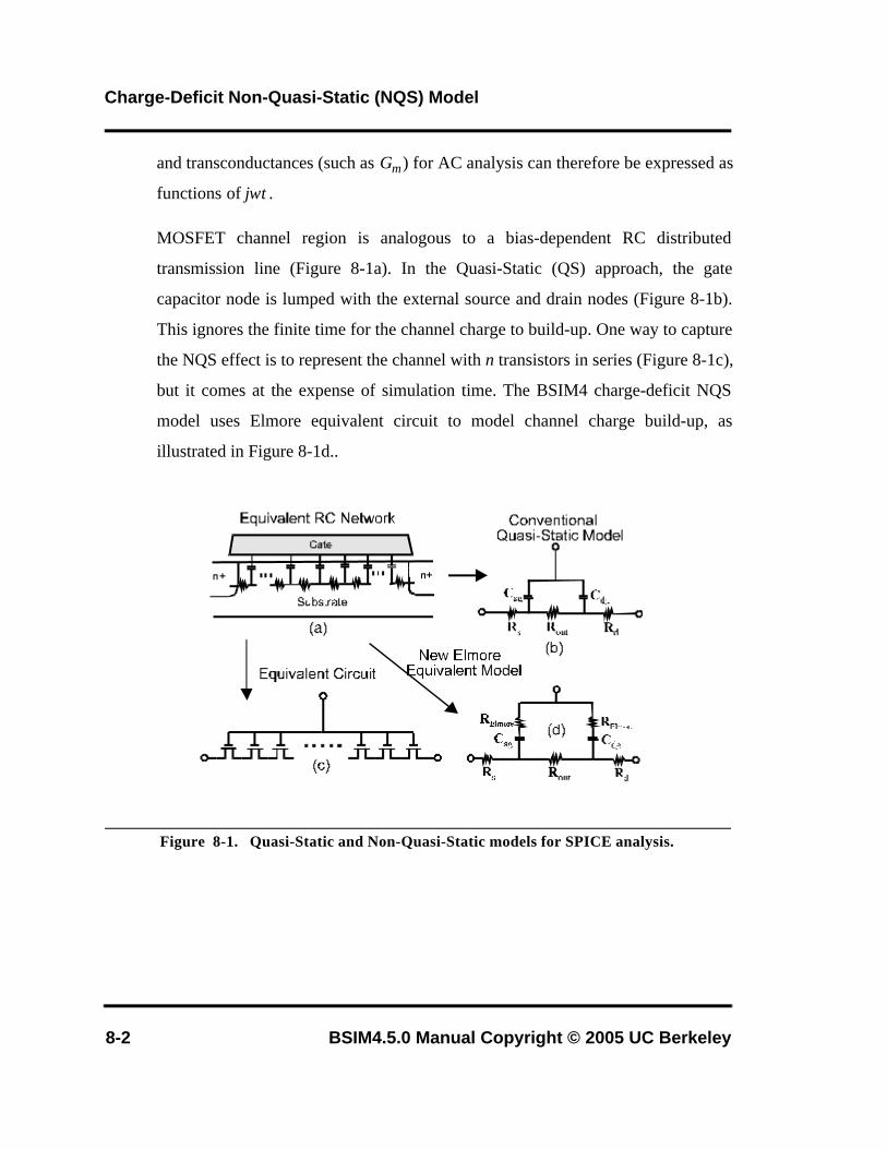
Charge-Deficit Non-Quasi-Static (NQS) Model
8-2 BSIM4.5.0 Manual Copyright © 2005 UC Berkeley
and transconductances (such as Gm) for AC analysis can therefore be expressed as
functions of jωτ.
MOSFET channel region is analogous to a bias-dependent RC distributed
transmission line (Figure 8-1a). In the Quasi-Static (QS) approach, the gate
capacitor node is lumped with the external source and drain nodes (Figure 8-1b).
This ignores the finite time for the channel charge to build-up. One way to capture
the NQS effect is to represent the channel with n transistors in series (Figure 8-1c),
but it comes at the expense of simulation time. The BSIM4 charge-deficit NQS
model uses Elmore equivalent circuit to model channel charge build-up, as
illustrated in Figure 8-1d..
Figure 8-1. Quasi-Static and Non-Quasi-Static models for SPICE analysis.
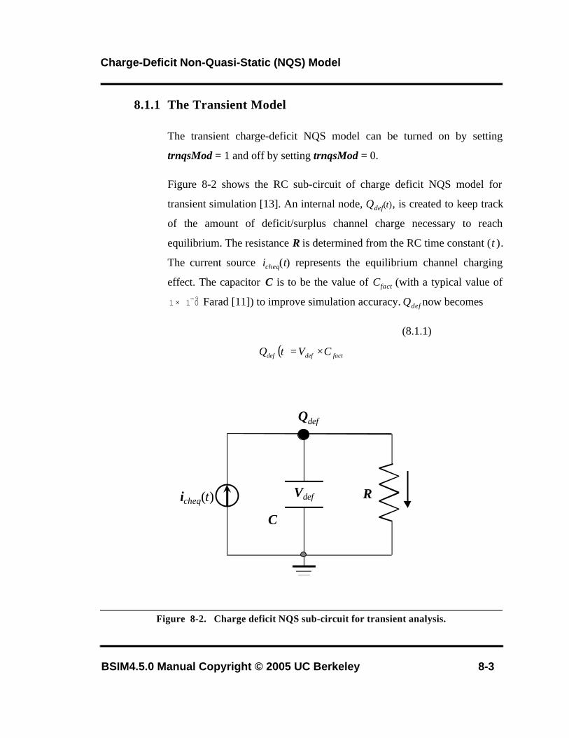
Charge-Deficit Non-Quasi-Static (NQS) Model
BSIM4.5.0 Manual Copyright © 2005 UC Berkeley 8-3
8.1.1 The Transient Model
The transient charge-deficit NQS model can be turned on by setting
trnqsMod = 1 and off by setting trnqsMod = 0.
Figure 8-2 shows the RC sub-circuit of charge deficit NQS model for
transient simulation [13]. An internal node, Qdef(t), is created to keep track
of the amount of deficit/surplus channel charge necessary to reach
equilibrium. The resistance R is determined from the RC time constant (τ).
The current source icheq(t) represents the equilibrium channel charging
effect. The capacitor C is to be the value of Cfact (with a typical value of
Farad [11]) to improve simulation accuracy. Qdef now becomes
(8.1.1)
Figure 8-2. Charge deficit NQS sub-circuit for transient analysis.
1 109–×
( ) factdefdef CVtQ ×=
icheq(t) R
C
Vdef
Qdef
Charge-Deficit Non-Quasi-Static (NQS) Model
8-4 BSIM4.5.0 Manual Copyright © 2005 UC Berkeley
Considering both the transport and charging component, the total current
related to the terminals D, G and S can be written as
(8.1.2)
Based on the relaxation time approach, the terminal charge and
corresponding charging current are modeled by
(8.1.3)
and
(8.1.4a)
(8.1.4b)
where D,G,Sxpart are charge deficit NQS channel charge partitioning
number for terminals D, G and S, respectively; Dxpart + Sxpart = 1 and Gxpart
= -1.
The transit time τ is equal to the product of Rii and WeffLeffCoxe, where Rii
is the intrinsic-input resistance [12] given by
( ) ( )( )
t
tQIti sgd
SGDSGD ∂
∂+= ,,
,,,, DC
( ) ( ) ( )tQtQtQ chcheqdef −=
( ) ( ) ( )τ
tQ
t
tQ
t
tQ defcheqdef −∂
∂=
∂
∂
( ) ( )τ
tQSGD
t
tQ defxpart
sgd ,,,, =∂
∂
Charge-Deficit Non-Quasi-Static (NQS) Model
BSIM4.5.0 Manual Copyright © 2005 UC Berkeley 8-5
(8.1.5)
where Coxeff is the effective gate dielectric capacitance calculated from the
DC model. Note that Rii in (8.1.5) considers both the drift and diffusion
componets of the channel conduction, each of which dominates in
inversion and subthreshold regions, respectively.
8.1.2 The AC Model
Similarly, the small-signal AC charge-deficit NQS model can be turned on
by setting acnqsMod = 1 and off by setting acnqsMod = 0.
For small signals, by substituting (8.1.3) into (8.1.4b), it is easy to show
that in the frequency domain, Qch(t) can be transformed into
(8.1.6)
where ω is the angular frequency. Based on (8.1.6), it can be shown that the
transcapacitances Cgi, Csi, and Cdi (i stands for any of the G, D, S and B
terminals of the device) and the channel transconductances Gm, Gds, and
Gmbs all become complex quantities. For example, now Gm have the form
of
⋅+⋅=
eff
Boxeffeffeff
dseff
ds
ii qLTkCW
XRCRGV
IXRCRG
Rµ
211
( ) ( )ωτj
tQtQ cheq
ch +
∆=∆
1
Gate Electrode Electrode and Intrinsic-Input Resistance (IIR) Model
BSIM4.5.0 Manual Copyright © 2005 UC Berkeley 8-6
(8.1.7)
and
(8.1.8)
Those quantities with sub “0” in the above two equations are known from
OP (operating point) analysis.
8.2 Gate Electrode Electrode and Intrinsic-Input Resistance (IIR) Model
8.2.1 General Description
BSIM4 provides four options for modeling gate electrode resistance (bias-
independent) and intrinsic-input resistance (IIR, bias-dependent). The IIR
model considers the relaxation-time effect due to the distributive RC nature
of the channel region, and therefore describes the first-order non-quasi-
static effect. Thus, the IIR model should not be used together with the
charge-deficit NQS model at the same time. The model selector rgateMod
is used to choose different options.
+⋅
−++
= 220
220
11 τωωτ
τωmm
mG
jG
G
+
⋅−+
+= 22
022
0
11 τω
ωτ
τωdgdg
dg
Cj
CC
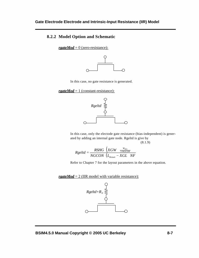
Gate Electrode Electrode and Intrinsic-Input Resistance (IIR) Model
BSIM4.5.0 Manual Copyright © 2005 UC Berkeley 8-7
8.2.2 Model Option and Schematic
rgateMod = 0 (zero-resistance):
In this case, no gate resistance is generated.
rgateMod = 1 (constant-resistance):
In this case, only the electode gate resistance (bias-independent) is gener-ated by adding an internal gate node. Rgeltd is give by
(8.1.9)
Refer to Chapter 7 for the layout parameters in the above equation.
rgateMod = 2 (IIR model with variable resistance):
Rgeltd
( )( ) NFXGLLNGCONXGWRSHG
Rgeltddrawn
NGCONWeffcj
⋅−⋅+⋅
= ⋅3
Rgeltd+Rii
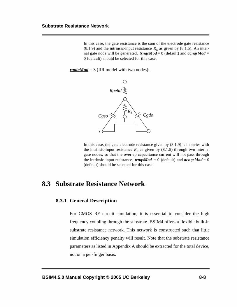
Substrate Resistance Network
BSIM4.5.0 Manual Copyright © 2005 UC Berkeley 8-8
In this case, the gate resistance is the sum of the electrode gate resistance(8.1.9) and the intrinsic-input resistance Ri i as given by (8.1.5). An inter-nal gate node will be generated. trnqsMod = 0 (default) and acnqsMod =0 (default) should be selected for this case.
rgateMod = 3 (IIR model with two nodes):
In this case, the gate electrode resistance given by (8.1.9) is in series withthe intrinsic-input resistance Rii as given by (8.1.5) through two internalgate nodes, so that the overlap capacitance current will not pass throughthe intrinsic-input resistance. trnqsMod = 0 (default) and acnqsMod = 0(default) should be selected for this case.
8.3 Substrate Resistance Network
8.3.1 General Description
For CMOS RF circuit simulation, it is essential to consider the high
frequency coupling through the substrate. BSIM4 offers a flexible built-in
substrate resistance network. This network is constructed such that little
simulation efficiency penalty will result. Note that the substrate resistance
parameters as listed in Appendix A should be extracted for the total device,
not on a per-finger basis.
Rii
Rgeltd
Cgso Cgdo
Substrate Resistance Network
BSIM4.5.0 Manual Copyright © 2005 UC Berkeley 8-9
8.3.2 Model Selector and Topology
The model selector rbodyMod can be used to turn on or turn off the
resistance network.
rbodyMod = 0 (Off):
No substrate resistance network is generated at all.
rbodyMod = 1 (On):
All five resistances in the substrate network as shown schematicallybelow are present simultaneously.
A minimum conductance, GBMIN, is introduced in parallel with each
resistance and therefore to prevent infinite resistance values, which would
otherwise cause poor convergence. In Figure 8-3, GBMIN is merged into
each resistance to simplify the representation of the model topology. Note
that the intrinsic model substrate reference point in this case is the internal
body node bNodePrime, into which the impact ionization current Iii and
the GIDL current IGIDL flow.
rbodyMod = 2 (On : Scalable Substrate Network):
The schematic is similar to rbodyMod = 1 but all the five resistors in thesubstrate network are now scalable with a possibility of chosing eitherfive resistors, three resistors or one resistor as the substrate network.
The resistors of the substrate network are scalable with respect to channel
length (L), channel width (W) and number of fingers (NF). The scalable
model allows to account for both horizontal and vertical contacts.
The scalable resistors RBPS and RBPD are evaluated through
Substrate Resistance Network
BSIM4.5.0 Manual Copyright © 2005 UC Berkeley 8-10
(8.1.10)
(8.1.11)
The resistor RBPB consists of two parallel resistor paths, one to the
horizontal contacts and other to the vertical contacts. These two resistances
are scalable and RBPB is given by a parallel combination of these two
resistances.
(8.1.12)
The resistors RBSB and RBDB share the same scaling parameters but have
different scaling prefactors. These resistors are modeled in the same way as
RBPB. The equations for RBSB are shown below. The calculation for
RBDB follows RBSB.
RBPSNFRBPSWRBPSL
NFWLRBPSRBPS •
•
•= −− 66 1010
0
RBPDNFRBPDWRBPDL
NFWLRBPDRBPD •
•
•= −− 66 1010
0
RBPBNFRBPBXWRBPBXL
NFWLRBPBXRBPBX •
•
•= −− 66 1010
0
RBPBYRBPBXRBPBYRBPBXRBPB
+•=
RBPBYNFRBPBYWRBPBYL
NFWLRBPBYRBPBY •
•
•= −− 66 1010
0
Substrate Resistance Network
BSIM4.5.0 Manual Copyright © 2005 UC Berkeley 8-11
(8.1.13)
The implementation of rbodyMod = 2 allows the user to chose between the
5-R network (with all five resistors), 3-R network (with RBPS, RBPD and
RBPB) and 1-R network (with only RBPB).
If the user doesn’t provide both the scaling parameters RBSBX0 and
RBSBY0 for RBSB OR both the scaling parameters RBDBX0 and RBDBY0
for RBDB, then the conductances for both RBSB and RBDB are set to
GBMIN. This converts the 5-R schematic to 3-R schematic where the
substrate network consists of the resistors RBPS, RBPD and RBPB. RBPS,
RBPD and RBPB are then calculated using (8.1.10), (8.1.11) and (8.1.12).
If the user chooses not to provide either of RBPS0 or RBPD0, then the 5-R
schematic is converted to 1-R network with only one resistor RBPB. The
conductances for RBSB and RBDB are set to GBMIN. The resistances
RBPS and RBPD are set to 1e-3 Ohm. The resistor RBPB is then calculated
using (8.1.12).
In all other situations, 5-R network is used with the resistor values
calculated from the equations aforementioned.
RBSDBXNFRBSDBXWRBSDBXL
NFWLRBSBXRBSBX •
•
•= −− 66 1010
0
RBSBYRBSBXRBSBYRBSBXRBSB
+•=
RBSDBXNFRBSDBXWRBSDBXL
NFWLRBSBXRBSBX •
•
•= −− 66 1010
0
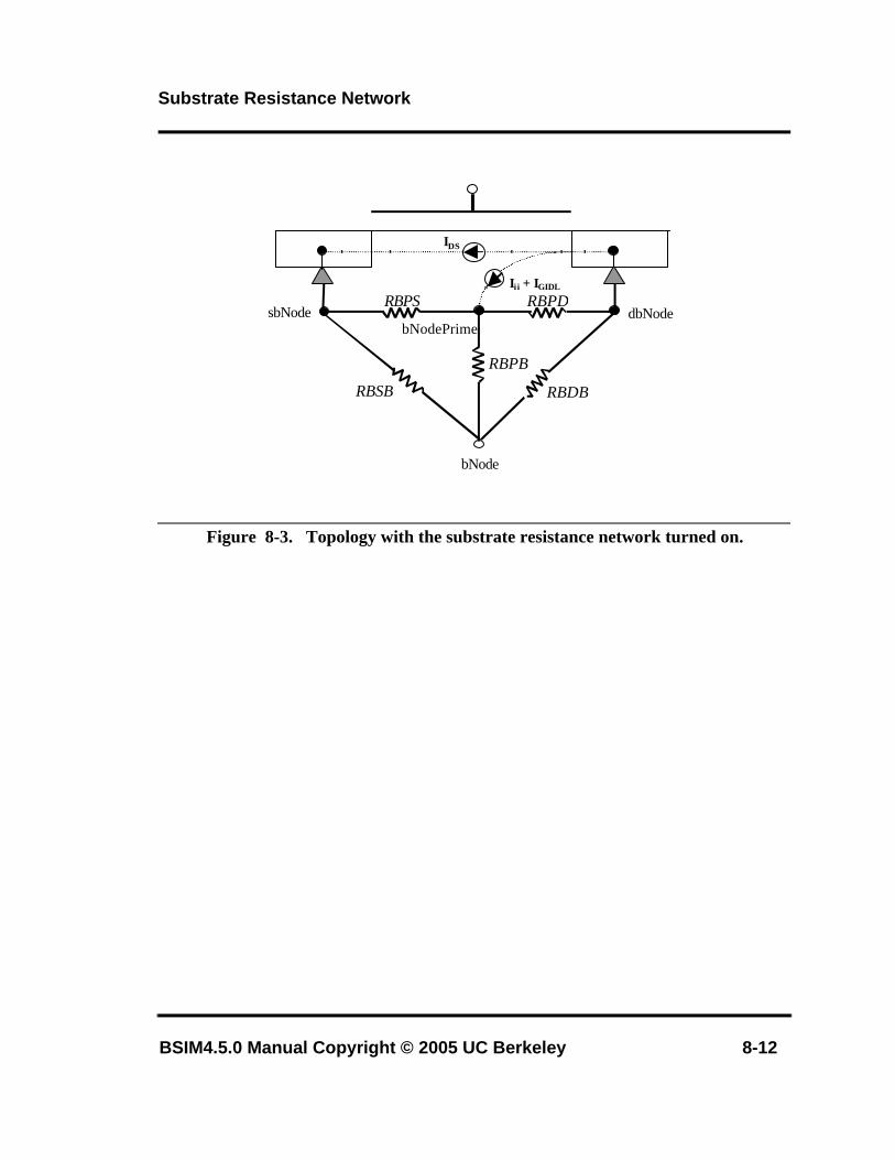
Substrate Resistance Network
BSIM4.5.0 Manual Copyright © 2005 UC Berkeley 8-12
Figure 8-3. Topology with the substrate resistance network turned on.
RBDB
RBPD
RBSB
RBPS
RBPB
Ii i + IGIDL
IDS
bNodePrimedbNodesbNode
bNode
BSIM4.5.0 Manual Copyright © 2005 UC Berkeley 9-1
Chapter 9: Noise Modeling
The following noise sources in MOSFETs are modeled in BSIM4 for SPICE noise
ananlysis: flicker noise (also known as 1/f noise), channel thermal noise and induced gate
noise and their correlation, thermal noise due to physical resistances such as the source/
drain, gate electrode, and substrate resistances, and shot noise due to the gate dielectric
tunneling current. A complete list of the noise model parameters and explanations are
given in Appendix A.
9.1 Flicker Noise Models
9.1.1 General Description
BSIM4 provides two flicker noise models. When the model selector
fnoiMod is set to 0, a simple flicker noise model which is convenient for
hand calculations is invoked. A unified physical flicker noise model, which
is the default model, will be used if fnoiMod = 1. These two modes come
from BSIM3v3, but the unified model has many improvements. For
instance, it is now smooth over all bias regions and considers the bulk
charge effect.
9.1.2 Equations
• fnoiMod = 0 (simple model)
Flicker Noise Models
9-2 BSIM4.5.0 Manual Copyright © 2005 UC Berkeley
The noise density is
(9.1.1)
where f is device operating frequency.
• fnoiMod = 1 (unified model)
The physical mechanism for the flicker noise is trapping/detrapping-related
charge fluctuation in oxide traps, which results in fluctuations of both
mobile carrier numbers and mobilities in the channel. The unified flicker
noise model captures this physical process.
In the inversion region, the noise density is expressed as [14]
(9.1.2)
where µeff is the effective mobility at the given bias condition, and Leff and
Weff are the effective channel length and width, respectively. The
parameter N0 is the charge density at the source side given by
( )EF
effoxe
AFds
idfLC
IKFfS 2
⋅=
( ) ( )
( )2
2
102
2
2200
0102
2
102
2102
*l
llef
effeff
clmdsB
ll*l
*
efbulkeffoxe
dseffBinv,id
NN
NNOICNNOIBNOIAf)LINTNOIL(W
LTIk
NNNOIC
NNNOIBNNNN
logNOIAfA)LINTNOIL(C
ITqk)f(S
+
⋅+⋅+⋅
⋅⋅−⋅∆
+
−+−⋅+
++
⋅⋅⋅−
=µ
Flicker Noise Models
BSIM4.5.0 Manual Copyright © 2005 UC Berkeley 9-3
(9.1.3)
The parameter Nl is the charge density at the drain end given by
(9.1.4)
N* is given by
(9.1.5)
where CIT is a model parameter from DC IV and Cd is the depletion
capacitance.
∆Lclm is the channel length reduction due to channel length modulation and
given by
(9.1.6)
In the subthreshold region, the noise density is written as
qVCN gsteffoxe ⋅=0
qV
VAVCN
tgsteff
dseffbulkgsteffoxel
+−⋅⋅=
ν21
( )2
*
qCITCCTkN doxeB ++⋅=
effsat
sat
dseffds
VSATE
E
EMLitl
VV
LitlL
µ2
logclm
=
+
−
⋅=∆
Channel Thermal Noise
9-4 BSIM4.5.0 Manual Copyright © 2005 UC Berkeley
(9.1.7)
The total flicker noise density is
(9.1.8)
9.2 Channel Thermal Noise
There are two channel thermal noise models in BSIM4. One is a charge-
based model (default model) similar to that used in BSIM3v3.2. The other
is the holistic model. These two models can be selected through the model
selector tnoiMod.
• tnoiMod = 0 (charge based)
The noise current is given by
(9.2.1)
where Rds(V) is the bias-dependent LDD source/drain resistance, and the
parameter NTNOI is introduced for more accurate fitting of short-channel
devices. Qinv is modeled by
( )102*
2
,10⋅
⋅⋅=
NfLW
ITkNOIAfS
EFeffeff
dsBsubVtid
( ) ( ) ( )( ) ( )fSfS
fSfSfS
invdsubvtid
subvtidinvdid
,i,
,,i
+×
=
( )NTNOI
VR
fTki
inveff
eff
QL
ds
Bd ⋅
+
∆=
µ
2
42
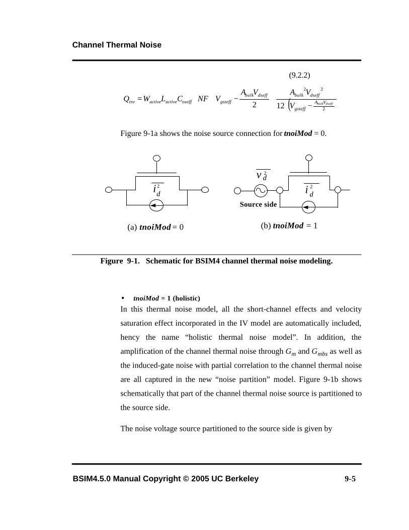
Channel Thermal Noise
BSIM4.5.0 Manual Copyright © 2005 UC Berkeley 9-5
(9.2.2)
Figure 9-1a shows the noise source connection for tnoiMod = 0.
Figure 9-1. Schematic for BSIM4 channel thermal noise modeling.
• tnoiMod = 1 (holistic)
In this thermal noise model, all the short-channel effects and velocity
saturation effect incorporated in the IV model are automatically included,
hency the name “holistic thermal noise model”. In addition, the
amplification of the channel thermal noise through Gm and Gmbs as well as
the induced-gate noise with partial correlation to the channel thermal noise
are all captured in the new “noise partition” model. Figure 9-1b shows
schematically that part of the channel thermal noise source is partitioned to
the source side.
The noise voltage source partitioned to the source side is given by
( )
−⋅+−⋅⋅=
2
22
122 dseffbulkVAgsteff
dseffbulkdseffbulkgsteffoxeffactiveactiveinv
V
VAVAVNFCLWQ
i 2
d
(a) tnoiMod = 0
v 2d
i 2
d
(b) tnoiMod = 1
Source side
Channel Thermal Noise
BSIM4.5.0 Manual Copyright © 2005 UC Berkeley 9-6
(9.2.3)
and the noise current source put in the channel region with gate and body
amplication is given by
(9.2.4)
where
(9.2.5)
and
(9.2.6)
where RNOIB and RNOIA are model parameters with default values 0.37
and 0.577 respectively.
ds
dsefftnoiBd I
fVTkv
∆⋅⋅= 22 4 θ
( )[ ]
( )22
22 4
mbsdsmd
mbsmtnoidsds
dseffBd
GGGv
GGGI
fVTki
++⋅−
+⋅+∆
= β
⋅⋅+⋅=
2
1effsat
gsteffefftnoi LE
VLTNOIBRNOIBθ
⋅⋅+⋅=
2
1effsat
gsteffefftnoi LE
VLTNOIARNOIAβ
Other Noise Sources Modeled
BSIM4.5.0 Manual Copyright © 2005 UC Berkeley 9-7
9.3 Other Noise Sources Modeled
BSIM4 also models the thermal noise due to the substrate, electrode gate, and
source/drain resistances. Shot noise due to various gate tunneling components is
modeled as well.
BSIM4.5.0 Manual Copyright © 2005 UC Berkeley 10-1
Chapter 10: Asymmetric MOS Junction Diode Models
10.1 Junction Diode IV Model
In BSIM4, there are three junction diode IV models. When the IV model selector
dioMod is set to 0 ("resistance-free"), the diode IV is modeled as resistance-free
with or without breakdown depending on the parameter values of XJBVS or
XJBVD. When dioMod is set to 1 ("breakdown-free"), the diode is modeled
exactly the same way as in BSIM3v3.2 with current-limiting feature in the
forward-bias region through the limiting current parameters IJTHSFWD or
IJTHDFWD; diode breakdown is not modeled for dioMod = 1 and XJBVS,
XJBVD, BVS, and BVD parameters all have no effect. When dioMod is set to 2
("resistance-and-breakdown"), BSIM4 models the diode breakdown with current
limiting in both forward and reverse operations. In general, setting dioMod to 1
produces fast convergence.
10.1.1 Source/Body Junction Diode
In the following, the equations for the source-side diode are given. The
model parameters are shown in Appendix A.
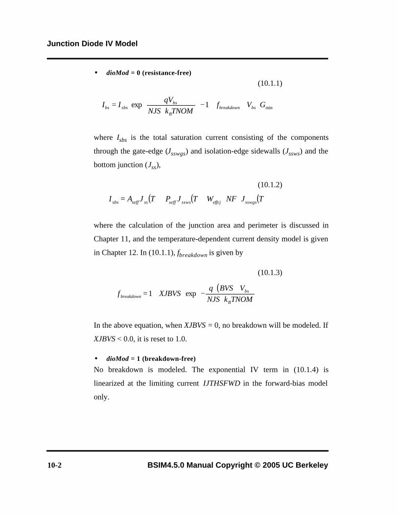
Junction Diode IV Model
10-2 BSIM4.5.0 Manual Copyright © 2005 UC Berkeley
• dioMod = 0 (resistance-free)
(10.1.1)
where Isbs is the total saturation current consisting of the components
through the gate-edge (Jsswgs) and isolation-edge sidewalls (Jssws) and the
bottom junction (Jss),
(10.1.2)
where the calculation of the junction area and perimeter is discussed in
Chapter 11, and the temperature-dependent current density model is given
in Chapter 12. In (10.1.1), fbreakdown is given by
(10.1.3)
In the above equation, when XJBVS = 0, no breakdown will be modeled. If
XJBVS < 0.0, it is reset to 1.0.
• dioMod = 1 (breakdown-free)
No breakdown is modeled. The exponential IV term in (10.1.4) is
linearized at the limiting current IJTHSFWD in the forward-bias model
only.
min1exp GVfTNOMkNJS
qVII bsbreakdown
B
bssbsbs ⋅+⋅
−
⋅
=
( ) ( ) ( )TJNFWTJPTJAI sswgseffcjsswsseffssseffsbs ⋅⋅++=
( )
⋅
+⋅−⋅+=
TNOMkNJSVBVSq
XJBVSfB
bsbreakdown exp1
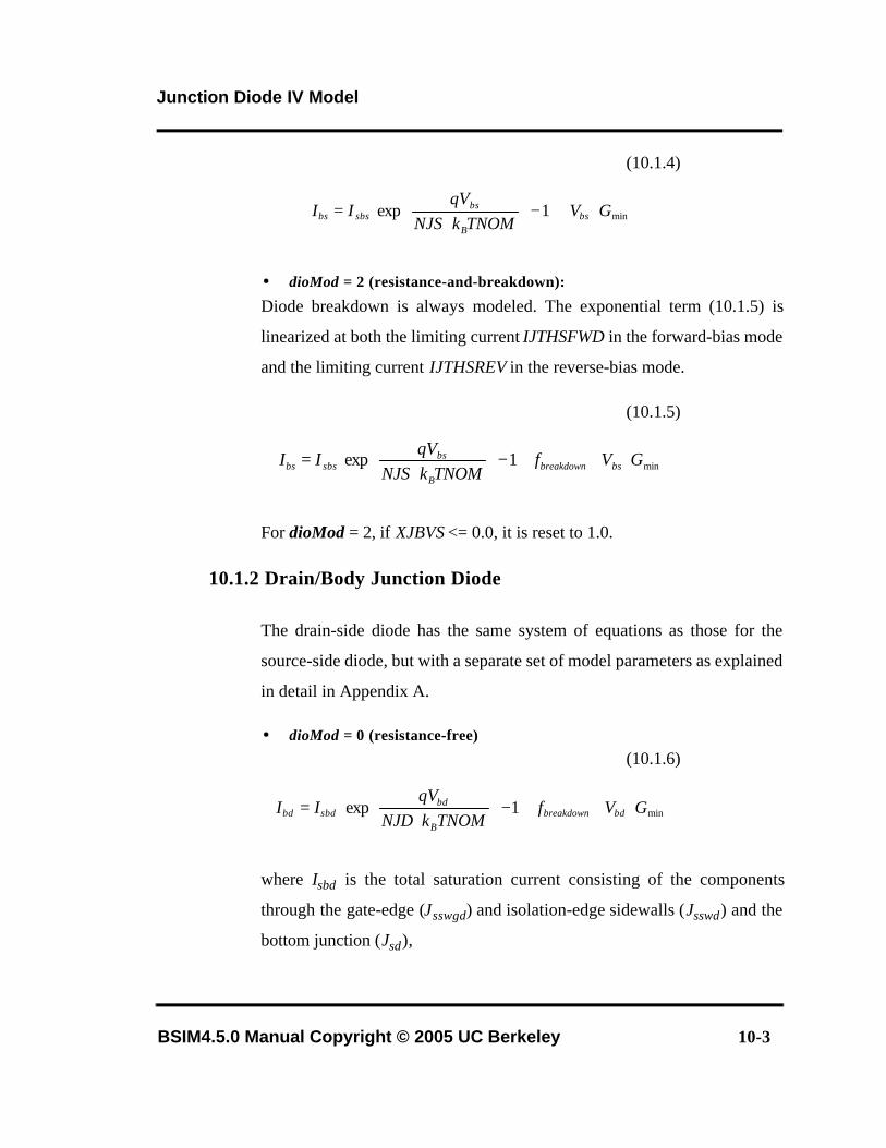
Junction Diode IV Model
BSIM4.5.0 Manual Copyright © 2005 UC Berkeley 10-3
(10.1.4)
• dioMod = 2 (resistance-and-breakdown):
Diode breakdown is always modeled. The exponential term (10.1.5) is
linearized at both the limiting current IJTHSFWD in the forward-bias mode
and the limiting current IJTHSREV in the reverse-bias mode.
(10.1.5)
For dioMod = 2, if XJBVS <= 0.0, it is reset to 1.0.
10.1.2 Drain/Body Junction Diode
The drain-side diode has the same system of equations as those for the
source-side diode, but with a separate set of model parameters as explained
in detail in Appendix A.
• dioMod = 0 (resistance-free)
(10.1.6)
where Isbd is the total saturation current consisting of the components
through the gate-edge (Jsswgd) and isolation-edge sidewalls (Jsswd) and the
bottom junction (Jsd),
min1exp GVTNOMkNJS
qVII bs
B
bssbsbs ⋅+
−
⋅
=
min1exp GVfTNOMkNJS
qVII bsbreakdown
B
bssbsbs ⋅+⋅
−
⋅
=
min1exp GVfTNOMkNJD
qVII bdbreakdown
B
bdsbdbd ⋅+⋅
−
⋅
=
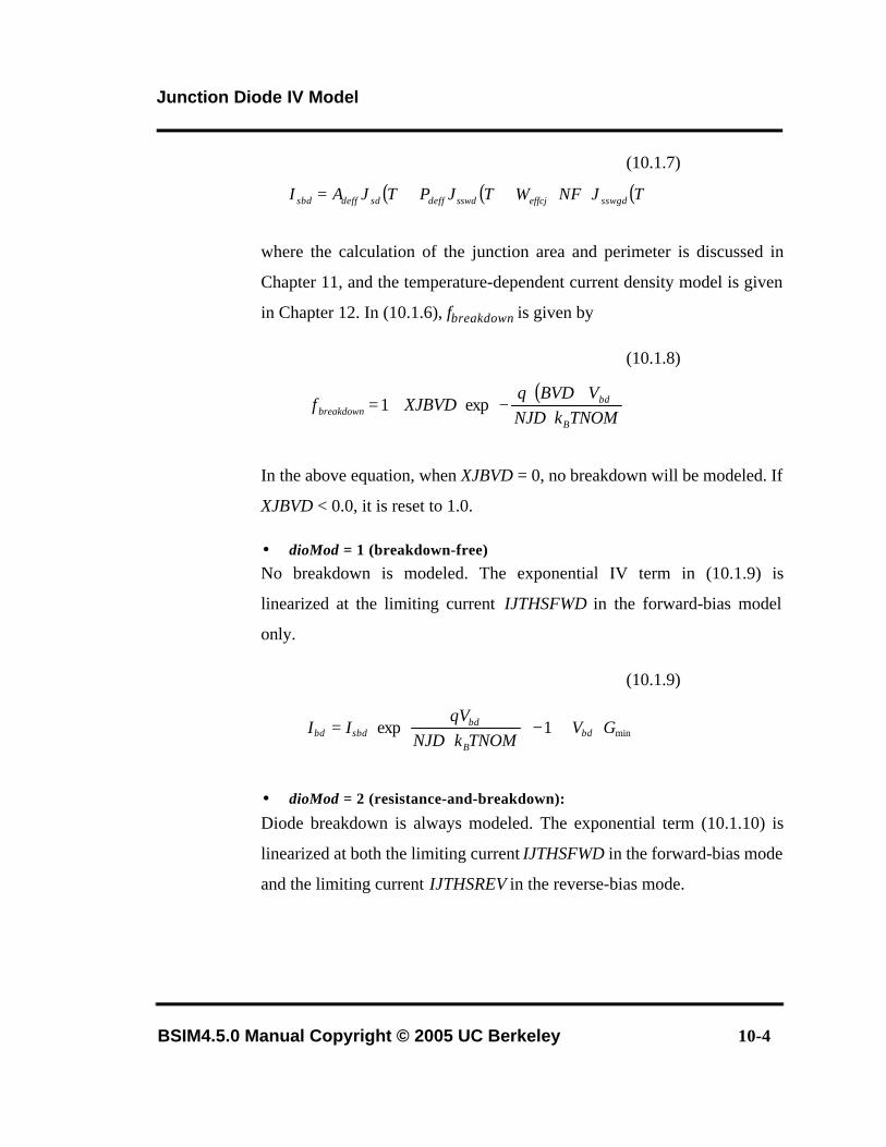
Junction Diode IV Model
BSIM4.5.0 Manual Copyright © 2005 UC Berkeley 10-4
(10.1.7)
where the calculation of the junction area and perimeter is discussed in
Chapter 11, and the temperature-dependent current density model is given
in Chapter 12. In (10.1.6), fbreakdown is given by
(10.1.8)
In the above equation, when XJBVD = 0, no breakdown will be modeled. If
XJBVD < 0.0, it is reset to 1.0.
• dioMod = 1 (breakdown-free)
No breakdown is modeled. The exponential IV term in (10.1.9) is
linearized at the limiting current IJTHSFWD in the forward-bias model
only.
(10.1.9)
• dioMod = 2 (resistance-and-breakdown):
Diode breakdown is always modeled. The exponential term (10.1.10) is
linearized at both the limiting current IJTHSFWD in the forward-bias mode
and the limiting current IJTHSREV in the reverse-bias mode.
( ) ( ) ( )TJNFWTJPTJAI sswgdeffcjsswddeffsddeffsbd ⋅⋅++=
( )
⋅
+⋅−⋅+=
TNOMkNJDVBVDq
XJBVDfB
bdbreakdown exp1
min1exp GVTNOMkNJD
qVII bd
B
bdsbdbd ⋅+
−
⋅
=
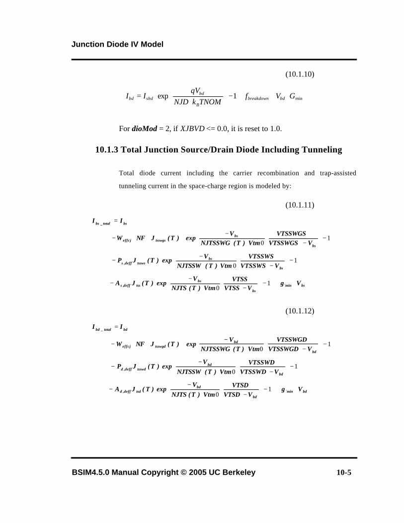
Junction Diode IV Model
BSIM4.5.0 Manual Copyright © 2005 UC Berkeley 10-5
(10.1.10)
For dioMod = 2, if XJBVD <= 0.0, it is reset to 1.0.
10.1.3 Total Junction Source/Drain Diode Including Tunneling
Total diode current including the carrier recombination and trap-assisted
tunneling current in the space-charge region is modeled by:
(10.1.11)
(10.1.12)
min1exp GVfTNOMkNJD
qVII bdbreakdown
B
bdsbdbd ⋅+⋅
−
⋅
=
bs`minbs
bstssdeff,s
bs
bstsswsdeff,s
bs
bstsswgseffcj
bstotal_bs
VgVVTSS
VTSSVtm)T(NJTS
Vexp)T(JA
VVTSSWSVTSSWS
Vtm)T(NJTSSWVexp)T(JP
VVTSSWGSVTSSWGS
Vtm)T(NJTSSWGV
exp)T(JNFW
II
⋅+
−
−
⋅⋅
−−
−
−
⋅⋅
−−
−
−
⋅⋅
−⋅⋅⋅−
=
10
10
10
bd`minbd
bdtsddeff,d
bd
bdtsswddeff,d
bd
bdtsswgdeffcj
bdtotal_bd
VgVVTSD
VTSDVtm)T(NJTS
Vexp)T(JA
VVTSSWDVTSSWD
Vtm)T(NJTSSWV
exp)T(JP
VVTSSWGDVTSSWGD
Vtm)T(NJTSSWGV
exp)T(JNFW
II
⋅+
−
−
⋅⋅
−−
−
−
⋅⋅
−−
−
−
⋅⋅
−⋅⋅⋅−
=
10
10
10
Junction Diode IV Model
BSIM4.5.0 Manual Copyright © 2005 UC Berkeley 10-6
Junction Diode CV Model
BSIM4.5.0 Manual Copyright © 2005 UC Berkeley 10-7
10.2 Junction Diode CV Model
Source and drain junction capacitances consist of three components: the bottom
junction capacitance, sidewall junction capacitance along the isolation edge, and
sidewall junction capacitance along the gate edge. An analogous set of equations
are used for both sides but each side has a separate set of model parameters.
10.2.1 Source/Body Junction Diode
The source-side junction capacitance can be calculated by
(10.2.1)
where Cjbs is the unit-area bottom S/B junciton capacitance, Cjbssw is the
unit-length S/B junction sidewall capacitance along the isolation edge, and
Cjbsswg is the unit-length S/B junction sidewall capacitance along the gate
edge. The effective area and perimeters in (10.2.1) are given in Chapter 11.
Cjbs is calculated by
if Vbs < 0
(10.2.2)
otherwise
jbsswgeffcjjbsswseffjbsseffbs CNFWCPCAC ⋅⋅++=
( ) ( )
MJS
bsjbs TPBS
VTCJSC
−
−⋅= 1
Junction Diode CV Model
10-8 BSIM4.5.0 Manual Copyright © 2005 UC Berkeley
(10.2.3)
Cjbssw is calculated by
if Vbs < 0
(10.2.4)
otherwise
(10.2.5)
Cjbsswg is calculated by
if Vbs < 0
(10.2.6)
otherwise
( ) ( )
⋅+⋅=
TPBSV
MJSTCJSC bsjbs 1
( ) ( )
MJSWS
bsjbssw TPBSWS
VTCJSWSC
−
−⋅= 1
( ) ( )
⋅+⋅=
TPBSWSV
MJSWSTCJSWSC bsjbssw 1
( ) ( )
MJSWGS
bsjbsswg TPBSWGS
VTCJSWGSC
−
−⋅= 1
Junction Diode CV Model
BSIM4.5.0 Manual Copyright © 2005 UC Berkeley 10-9
(10.2.7)
10.2.2 Drain/Body Junction Diode
The drain-side junction capacitance can be calculated by
(10.2.8)
where Cjbd is the unit-area bottom D/B junciton capacitance, Cjbdsw is the
unit-length D/B junction sidewall capacitance along the isolation edge, and
Cjbdswg is the unit-length D/B junction sidewall capacitance along the gate
edge. The effective area and perimeters in (10.2.8) are given in Chapter 11.
Cjbd is calculated by
if Vbd < 0
(10.2.9)
otherwise
(10.2.10)
( ) ( )
MJSWGS
bsjbsswg TPBSWGS
VTCJSWGSC
−
−⋅= 1
jbdswgeffcjjbdswdeffjbddeffbd CNFWCPCAC ⋅⋅++=
( ) ( )
MJD
bdjbd TPBD
VTCJDC
−
−⋅= 1
( ) ( )
⋅+⋅=
TPBDV
MJDTCJDC bdjbd 1
Junction Diode CV Model
10-10 BSIM4.5.0 Manual Copyright © 2005 UC Berkeley
Cjbdsw is calculated by
if Vbd < 0
(10.2.11)
otherwise
(10.2.12)
Cjbdswg is calculated by
if Vbd < 0
(10.2.13)
otherwise
(10.2.14)
( ) ( )
MJSWD
bdjbdsw TPBSWD
VTCJSWDC
−
−⋅= 1
( ) ( )
⋅+⋅=
TPBSWDV
MJSWDTCJSWDC bdjbdsw 1
( ) ( )
MJSWGD
bdjbdswg TPBSWGD
VTCJSWGDC
−
−⋅= 1
( ) ( )
⋅+⋅=
TPBSWGDV
MJSWGDTCJSWGDC bdjbdswg 1
BSIM4.5.0 Manual Copyright © 2005 UC Berkeley 11-1
Chapter 11: Layout-Dependent Parasitics Model
BSIM4 provides a comprehensive and versatile geometry/layout-dependent parasitcs
model [15]. It supports modeling of series (such as isolated, shared, or merged source/
drain) and multi-finger device layout, or a combination of these two configurations. This
model have impact on every BSIM4 sub-models except the substrate resistance network
model. Note that the narrow-width effect in the per-finger device with multi-finger
configuration is accounted for by this model. A complete list of model parameters and
selectors can be found in Appendix A.
11.1 Geometry Definition
Figure 11-1 schematically shows the geometry definition for various source/drain
connections and source/drain/gate contacts. The layout parameters shown in this
figure will be used to calculate resistances and source/drain perimeters and areas.
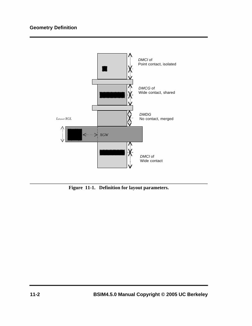
Geometry Definition
11-2 BSIM4.5.0 Manual Copyright © 2005 UC Berkeley
Figure 11-1. Definition for layout parameters.
DMCI ofPoint contact, isolated
DMCG ofWide contact, shared
DMDGNo contact, merged
DMCI ofWide contact
XGW
Ldrawn-XGL
Model Formulation and Options
BSIM4.5.0 Manual Copyright © 2005 UC Berkeley 11-3
11.2 Model Formulation and Options
11.2.1 Effective Junction Perimeter and Area
In the following, only the source-side case is illustrated. The same
approach is used for the drain side. The effective junction perimeter on the
source side is calculated by
The effective junction area on the source side is calculated by
In the above, Pseff and Aseff will be used to calculate junction diode IV and
CV. Pseff does not include the gate-edge perimeter.
If (PS is given) if (perMod == 0) Pseff = PS else NFWPSP effcjseff ⋅−=
Else Pseff computed from NF, DWJ, geoMod, DMCG, DMCI, DMDG, DMCGT, and MIN.
If (AS is given) Aseff = ASElse Aseff computed from NF, DWJ, geoMod, DMCG, DMCI, DMDG, DMCGT, and MIN.
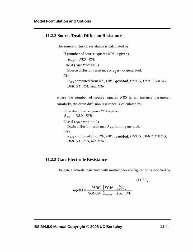
Model Formulation and Options
BSIM4.5.0 Manual Copyright © 2005 UC Berkeley 11-4
11.2.2 Source/Drain Diffusion Resistance
The source diffusion resistance is calculated by
where the number of source squares NRS is an instance parameter.
Similarly, the drain diffusion resistance is calculated by
11.2.3 Gate Electrode Resistance
The gate electrode resistance with multi-finger configuration is modeled by
(11.2.1)
If (number of source squares NRS is given) RSHNRSRsdiff ⋅=
Else if (rgeoMod == 0) Source diffusion resistance Rsdiff is not generated. Else Rsdiff computed from NF, DWJ, geoMod, DMCG, DMCI, DMDG, DMCGT, RSH, and MIN.
If (number of source squares NRD is given)
RSHNRDRddiff ⋅=
Else if (rgeoMod == 0) Drain diffusion resistance Rddiff is not generated. Else Rddiff computed from NF, DWJ, geoMod, DMCG , DMCI, DMDG, DMCGT, RSH, and MIN .
( )( ) NFXGLLNGCONXGWRSHG
Rgeltddrawn
NGCONWeffcj
⋅−⋅+⋅
= ⋅3
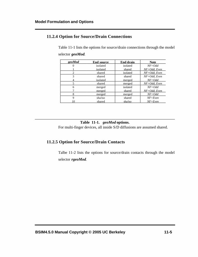
Model Formulation and Options
BSIM4.5.0 Manual Copyright © 2005 UC Berkeley 11-5
11.2.4 Option for Source/Drain Connections
Table 11-1 lists the options for source/drain connections through the model
selector geoMod.
Table 11-1. geoMod options.For multi-finger devices, all inside S/D diffusions are assumed shared.
11.2.5 Option for Source/Drain Contacts
Talbe 11-2 lists the options for source/drain contacts through the model
selector rgeoMod.
geoMod End source End drain Note0 isolated isolated NF=Odd1 isolated shared NF=Odd, Even2 shared isolated NF=Odd, Even3 shared shared NF=Odd, Even4 isolated merged NF=Odd5 shared merged NF=Odd, Even6 merged isolated NF=Odd7 merged shared NF=Odd, Even8 merged merged NF=Odd9 sha/iso shared NF=Even10 shared sha/iso NF=Even
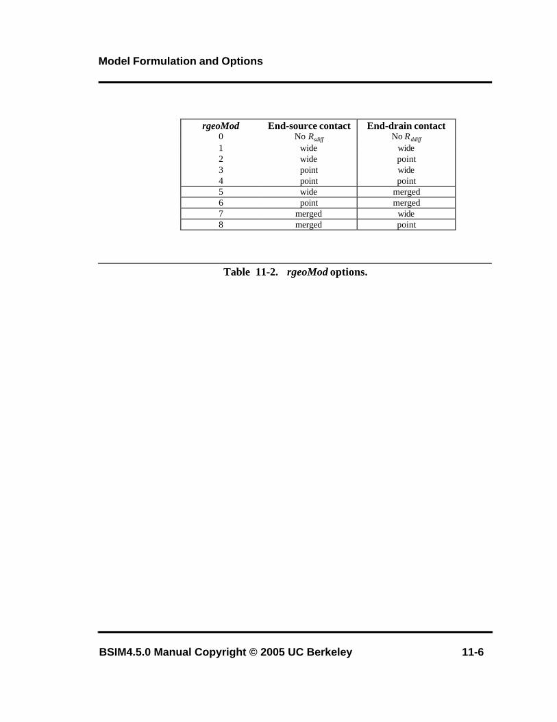
Model Formulation and Options
BSIM4.5.0 Manual Copyright © 2005 UC Berkeley 11-6
Table 11-2. rgeoMod options.
rgeoMod End-source contact End-drain contact0 No Rsdiff No Rddiff
1 wide wide2 wide point3 point wide4 point point5 wide merged6 point merged7 merged wide8 merged point
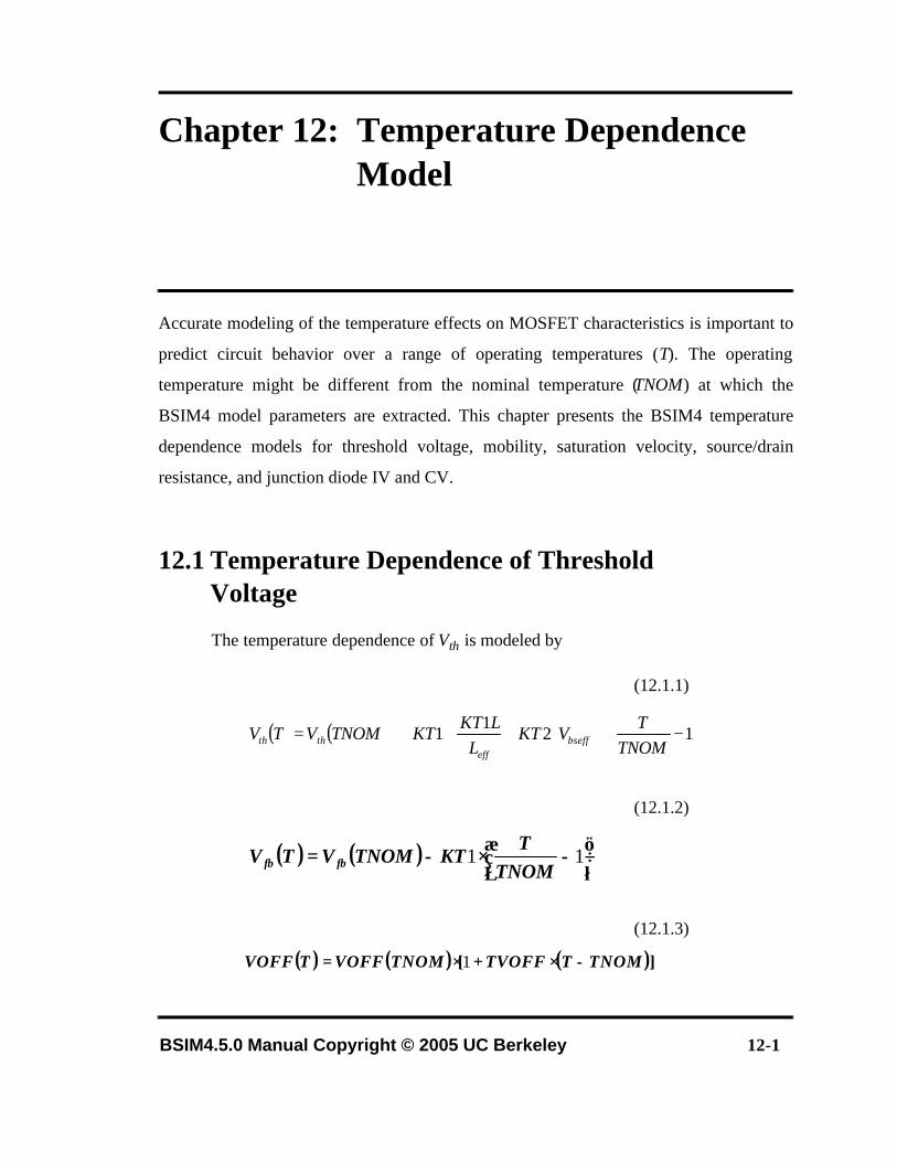
BSIM4.5.0 Manual Copyright © 2005 UC Berkeley 12-1
Chapter 12: Temperature Dependence Model
Accurate modeling of the temperature effects on MOSFET characteristics is important to
predict circuit behavior over a range of operating temperatures (T). The operating
temperature might be different from the nominal temperature (TNOM) at which the
BSIM4 model parameters are extracted. This chapter presents the BSIM4 temperature
dependence models for threshold voltage, mobility, saturation velocity, source/drain
resistance, and junction diode IV and CV.
12.1 Temperature Dependence of Threshold Voltage
The temperature dependence of Vth is modeled by
(12.1.1)
(12.1.2)
(12.1.3)
( ) ( )
−⋅
⋅+++= 12
11
TNOMT
VKTL
LKTKTTNOMVTV bseff
effthth
( ) ( )
−⋅−= 11
TNOMT
KTTNOMVTV fbfb
( ) ( ) ( )][ TNOMTTVOFFTNOMVOFFTVOFF −⋅+⋅= 1
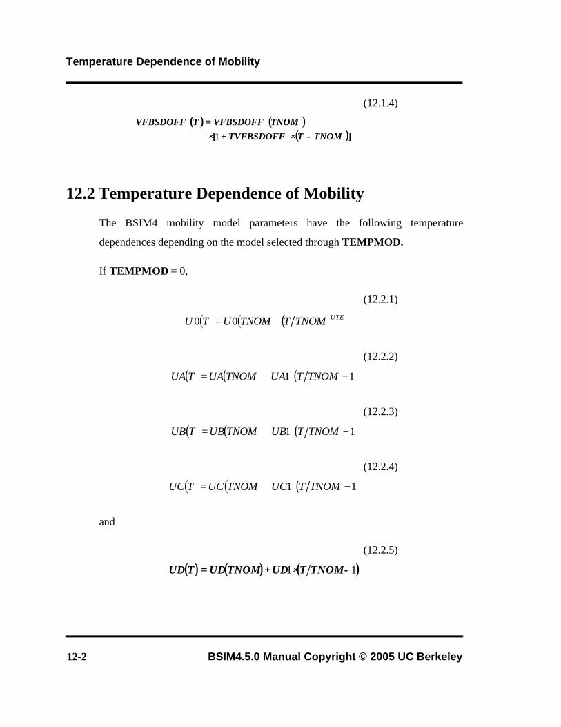
Temperature Dependence of Mobility
12-2 BSIM4.5.0 Manual Copyright © 2005 UC Berkeley
(12.1.4)
12.2 Temperature Dependence of Mobility
The BSIM4 mobility model parameters have the following temperature
dependences depending on the model selected through TEMPMOD.
If TEMPMOD = 0,
(12.2.1)
(12.2.2)
(12.2.3)
(12.2.4)
and
(12.2.5)
( ) ( )( )][ TNOMTTVFBSDOFF
TNOMVFBSDOFFTVFBSDOFF
−⋅+⋅=
1
( ) ( ) ( )UTETNOMTTNOMUTU ⋅= 00
( ) ( ) ( )11 −⋅+= TNOMTUATNOMUATUA
( ) ( ) ( )11 −⋅+= TNOMTUBTNOMUBTUB
( ) ( ) ( )11 −⋅+= TNOMTUCTNOMUCTUC
( ) ( ) ( )11 −⋅+= TNOMTUDTNOMUDTUD
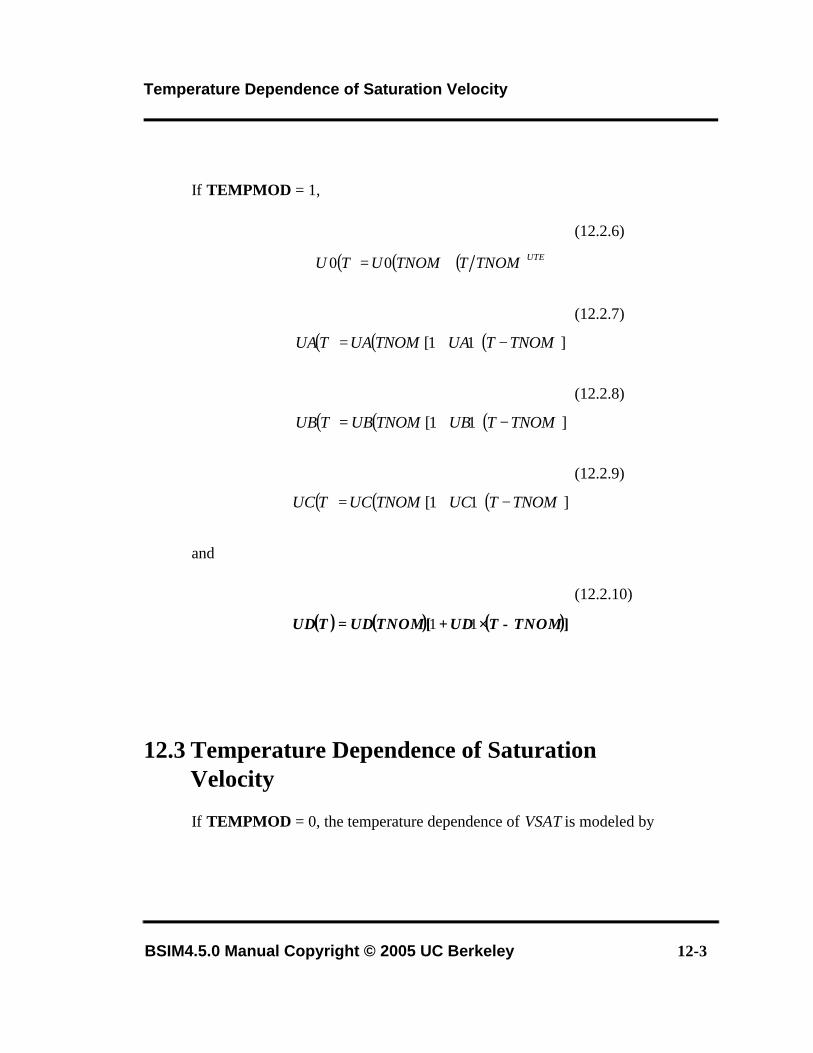
Temperature Dependence of Saturation Velocity
BSIM4.5.0 Manual Copyright © 2005 UC Berkeley 12-3
If TEMPMOD = 1,
(12.2.6)
(12.2.7)
(12.2.8)
(12.2.9)
and
(12.2.10)
12.3 Temperature Dependence of Saturation Velocity
If TEMPMOD = 0, the temperature dependence of VSAT is modeled by
( ) ( ) ( )UTETNOMTTNOMUTU ⋅= 00
( ) ( ) ( )]11[ TNOMTUATNOMUATUA −⋅+=
( ) ( ) ( )]11[ TNOMTUBTNOMUBTUB −⋅+=
( ) ( ) ( )]11[ TNOMTUCTNOMUCTUC −⋅+=
( ) ( ) ( )][ TNOMTUDTNOMUDTUD −⋅+= 11
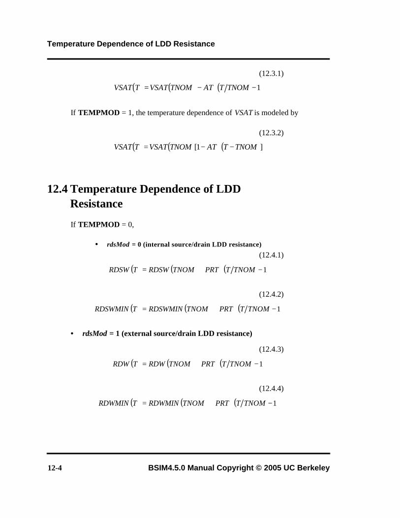
Temperature Dependence of LDD Resistance
12-4 BSIM4.5.0 Manual Copyright © 2005 UC Berkeley
(12.3.1)
If TEMPMOD = 1, the temperature dependence of VSAT is modeled by
(12.3.2)
12.4 Temperature Dependence of LDD Resistance
If TEMPMOD = 0,
• rdsMod = 0 (internal source/drain LDD resistance)
(12.4.1)
(12.4.2)
• rdsMod = 1 (external source/drain LDD resistance)
(12.4.3)
(12.4.4)
( ) ( ) ( )1−⋅−= TNOMTATTNOMVSATTVSAT
( ) ( ) ( )]1[ TNOMTATTNOMVSATTVSAT −⋅−=
( ) ( ) ( )1−⋅+= TNOMTPRTTNOMRDSWTRDSW
( ) ( ) ( )1−⋅+= TNOMTPRTTNOMRDSWMINTRDSWMIN
( ) ( ) ( )1−⋅+= TNOMTPRTTNOMRDWTRDW
( ) ( ) ( )1−⋅+= TNOMTPRTTNOMRDWMINTRDWMIN
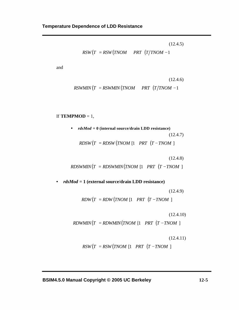
Temperature Dependence of LDD Resistance
BSIM4.5.0 Manual Copyright © 2005 UC Berkeley 12-5
(12.4.5)
and
(12.4.6)
If TEMPMOD = 1,
• rdsMod = 0 (internal source/drain LDD resistance)
(12.4.7)
(12.4.8)
• rdsMod = 1 (external source/drain LDD resistance)
(12.4.9)
(12.4.10)
(12.4.11)
( ) ( ) ( )1−⋅+= TNOMTPRTTNOMRSWTRSW
( ) ( ) ( )1−⋅+= TNOMTPRTTNOMRSWMINTRSWMIN
( ) ( ) ( )]1[ TNOMTPRTTNOMRDSWTRDSW −⋅+=
( ) ( ) ( )]1[ TNOMTPRTTNOMRDSWMINTRDSWMIN −⋅+=
( ) ( ) ( )]1[ TNOMTPRTTNOMRDWTRDW −⋅+=
( ) ( ) ( )]1[ TNOMTPRTTNOMRDWMINTRDWMIN −⋅+=
( ) ( ) ( )]1[ TNOMTPRTTNOMRSWTRSW −⋅+=
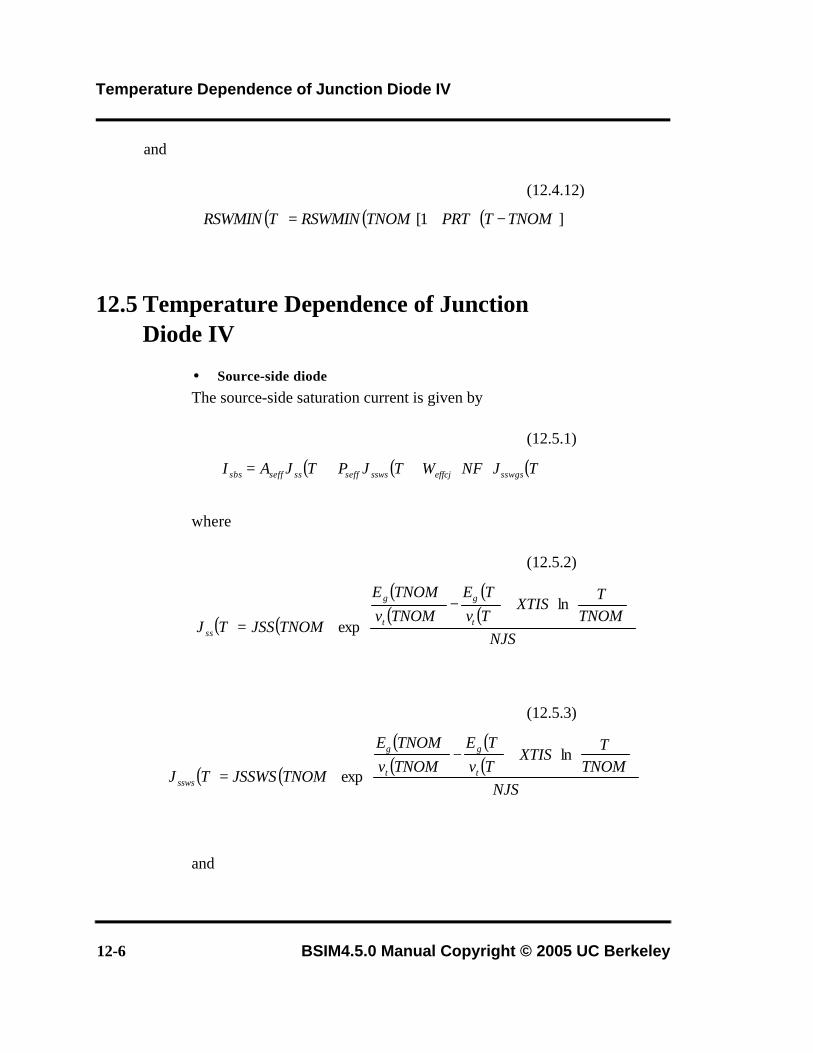
Temperature Dependence of Junction Diode IV
12-6 BSIM4.5.0 Manual Copyright © 2005 UC Berkeley
and
(12.4.12)
12.5 Temperature Dependence of Junction Diode IV
• Source-side diode
The source-side saturation current is given by
(12.5.1)
where
(12.5.2)
(12.5.3)
and
( ) ( ) ( )]1[ TNOMTPRTTNOMRSWMINTRSWMIN −⋅+=
( ) ( ) ( )TJNFWTJPTJAI sswgseffcjsswsseffssseffsbs ⋅⋅++=
( ) ( )
( )( )
( )( )
⋅+−
⋅=NJS
TNOMT
XTISTvTE
TNOMvTNOME
TNOMJSSTJ t
g
t
g
ss
lnexp
( ) ( )
( )( )
( )( )
⋅+−
⋅=NJS
TNOMT
XTISTvTE
TNOMvTNOME
TNOMJSSWSTJ t
g
t
g
ssws
lnexp
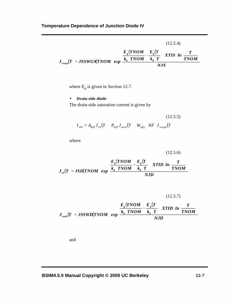
Temperature Dependence of Junction Diode IV
BSIM4.5.0 Manual Copyright © 2005 UC Berkeley 12-7
(12.5.4)
where Eg is given in Section 12.7.
• Drain-side diode
The drain-side saturation current is given by
(12.5.5)
where
(12.5.6)
(12.5.7)
and
( ) ( )
( ) ( )
⋅+⋅
−⋅⋅=
NJSTNOM
TlnXTISTk
TE
TNOMk
TNOME
expTNOMJSSWGSTJ b
g
b
g
sswgs
( ) ( ) ( )TJNFWTJPTJAI sswgdeffcjsswddeffsddeffsbd ⋅⋅++=
( ) ( )
( ) ( )
⋅+⋅
−⋅⋅=
NJDTNOM
TlnXTIDTk
TE
TNOMk
TNOME
expTNOMJSDTJ b
g
b
g
sd
( ) ( )
( ) ( )
⋅+
⋅−
⋅⋅=
NJDTNOM
TlnXTID
Tk
TE
TNOMk
TNOME
expTNOMJSSWDTJ b
g
b
g
sswd
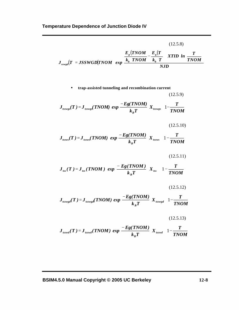
Temperature Dependence of Junction Diode IV
BSIM4.5.0 Manual Copyright © 2005 UC Berkeley 12-8
(12.5.8)
• trap-assisted tunneling and recombination current
(12.5.9)
(12.5.10)
(12.5.11)
(12.5.12)
(12.5.13)
( ) ( )
( ) ( )
⋅+⋅
−⋅⋅=
NJDTNOM
TlnXTIDTk
TE
TNOMk
TNOME
expTNOMJSSWGDTJ b
g
b
g
sswgd
−⋅⋅
−⋅=
TNOMT
XTk
)TNOM(Egexp)TNOM(J)T(J tsswgs
Btsswgstsswgs 1
−⋅⋅−⋅=
TNOMT
XTk
)TNOM(Egexp)TNOM(J)T(J tssws
Btsswstssws 1
−⋅⋅−⋅=
TNOMT
XTk
)TNOM(Egexp)TNOM(J)T(J tss
Btsstss 1
−⋅⋅
−⋅=
TNOMT
XTk
)TNOM(Egexp)TNOM(J)T(J tsswgd
Btsswgdtsswgd 1
−⋅⋅
−⋅=
TNOMT
XTk
)TNOM(Egexp)TNOM(J)T(J tsswd
Btsswdtsswd 1
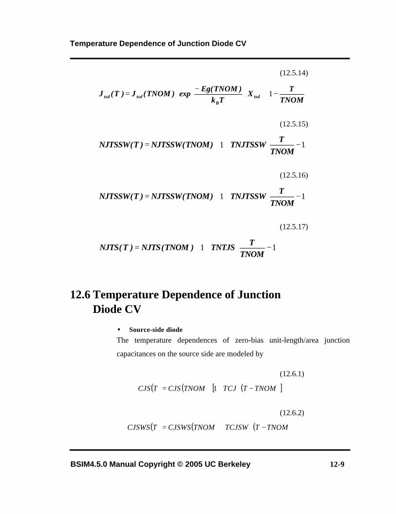
Temperature Dependence of Junction Diode CV
BSIM4.5.0 Manual Copyright © 2005 UC Berkeley 12-9
(12.5.14)
(12.5.15)
(12.5.16)
(12.5.17)
12.6 Temperature Dependence of Junction Diode CV
• Source-side diode
The temperature dependences of zero-bias unit-length/area junction
capacitances on the source side are modeled by
(12.6.1)
(12.6.2)
−⋅⋅−⋅=
TNOMT
XTk
)TNOM(Egexp)TNOM(J)T(J tsd
Btsdtsd 1
−+⋅= 11TNOM
TTNJTSSW)TNOM(NJTSSW)T(NJTSSW
−+⋅= 11TNOM
TTNJTSSW)TNOM(NJTSSW)T(NJTSSW
−+⋅= 11
TNOMTTNTJS)TNOM(NJTS)T(NJTS
( ) ( ) ( )[ ]TNOMTTCJTNOMCJSTCJS −⋅+⋅= 1
( ) ( ) ( )TNOMTTCJSWTNOMCJSWSTCJSWS −⋅+=
Temperature Dependence of Junction Diode CV
BSIM4.5.0 Manual Copyright © 2005 UC Berkeley 12-10
and
(12.6.3)
The temperature dependences of the built-in potentials on the source side are
modeled by
(12.6.4)
(12.6.5)
and
(12.6.6)
• Drain-side diode
The temperature dependences of zero-bias unit-length/area junction
capacitances on the drain side are modeled by
(12.6.7)
(12.6.8)
and
( ) ( ) ( )[ ]TNOMTTCJSWGTNOMCJSWGSTCJSWGS −⋅+⋅= 1
( ) ( ) ( )TNOMTTPBTNOMPBSTPBS −⋅−=
( ) ( ) ( )TNOMTTPBSWTNOMPBSWSTPBSWS −⋅−=
( ) ( ) ( )TNOMTTPBSWGTNOMPBSWGSTPBSWGS −⋅−=
( ) ( ) ( )[ ]TNOMTTCJTNOMCJDTCJD −⋅+⋅= 1
( ) ( ) ( )TNOMTTCJSWTNOMCJSWDTCJSWD −⋅+=
Temperature Dependences of Eg and ni
BSIM4.5.0 Manual Copyright © 2005 UC Berkeley 12-11
(12.6.9)
The temperature dependences of the built-in potentials on the drain side are
modeled by
(12.6.10)
(12.6.11)
and
(12.6.12)
12.7 Temperature Dependences of Eg and ni
• Energy-band gap of Si (Eg)
The temperature dependence of Eg is modeled by
(12.7.1)
and
( ) ( ) ( )[ ]TNOMTTCJSWGTNOMCJSWGDTCJSWGD −⋅+⋅= 1
( ) ( ) ( )TNOMTTPBTNOMPBDTPBD −⋅−=
( ) ( ) ( )TNOMTTPBSWTNOMPBSWDTPBSWD −⋅−=
( ) ( ) ( )TNOMTTPBSWGTNOMPBSWGDTPBSWGD −⋅−=
( )1108
1002.716.1
24
+×
−=−
TNOMTNOM
TNOMEg
Temperature Dependences of Eg and ni
BSIM4.5.0 Manual Copyright © 2005 UC Berkeley 12-12
(12.7.2)
• Intrinsic carrier concentration of Si (ni)
The temperature dependence of ni is modeled by
(12.7.3)
( )11081002.7
16.124
+×
−=−
TT
TEg
( )
⋅
−⋅⋅⋅=Tk
TNOMqETNOMTNOMen
B
gi 2
5565981.21exp15.30015.300
1045.1
BSIM4.5.0 Manual Copyright © 2005 UC Berkeley 13-1
Chapter 13: Stress Effect Model
CMOS feature size aggressively scaling makes shallow trench isolation(STI) very
popular active area isolatiohn process in advanced technologies. Recent years, strain
channel materials have been employed to achieve high device performance. The
mechanical stress effect induced by these process causes MOSFET performance
function of the active area size(OD: oxide definition) and the location of the device
in the active area. And the necessity of new models to describe the layout
dependence of MOS parameters due to stress effect becomes very urgent in advance
CMOS technologies.
Influence of stress on mobility has been well known since the 0.13um technology.
The stress influence on saturation velocity is also experimentally demonstrated.
Stress-induced enhancement or suppression of dopant diffusion during the
processing is reported. Since the doping profile may be changed due to different STI
sizes and stress, the threshold voltage shift and changes of other second-order
effects, such as DIBL and body effect, were shown in process integration.
BSIM4 considers the influence of stress on mobility, velocity saturation, threshold
voltage, body effect, and DIBL effect.
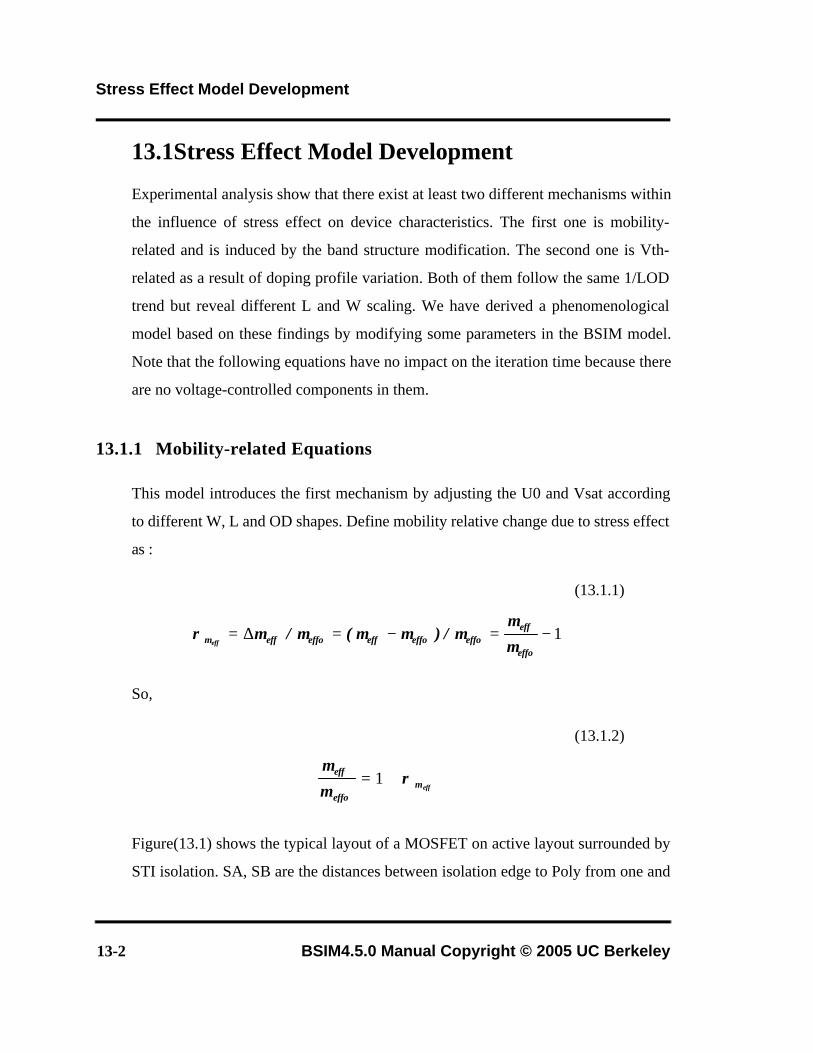
Stress Effect Model Development
13-2 BSIM4.5.0 Manual Copyright © 2005 UC Berkeley
13.1Stress Effect Model Development
Experimental analysis show that there exist at least two different mechanisms within
the influence of stress effect on device characteristics. The first one is mobility-
related and is induced by the band structure modification. The second one is Vth-
related as a result of doping profile variation. Both of them follow the same 1/LOD
trend but reveal different L and W scaling. We have derived a phenomenological
model based on these findings by modifying some parameters in the BSIM model.
Note that the following equations have no impact on the iteration time because there
are no voltage-controlled components in them.
13.1.1 Mobility-related Equations
This model introduces the first mechanism by adjusting the U0 and Vsat according
to different W, L and OD shapes. Define mobility relative change due to stress effect
as :
(13.1.1)
So,
(13.1.2)
Figure(13.1) shows the typical layout of a MOSFET on active layout surrounded by
STI isolation. SA, SB are the distances between isolation edge to Poly from one and
1−=−=∆=effo
effeffoeffoeffeffoeff /)(/
eff µ
µµµµµµρ µ
eff
effo
effµρ
µ
µ+= 1

Stress Effect Model Development
BSIM4.5.0 Manual Copyright © 2005 UC Berkeley 13-3
the other side, respectively. 2D simulation shows that stress distribution can be
expressed by a simple function of SA and SB.
Fig. (13.1) shows the typical layout of a MOSFET
Fig. (13.2) Stress distribution within MOSFET channel using 2D simulation
W
LTrench
isolation edge
SA SB
LOD
W
LTrench
isolation edge
SA SB
LOD
LSBSALOD ++= OD: gate Oxide Definition
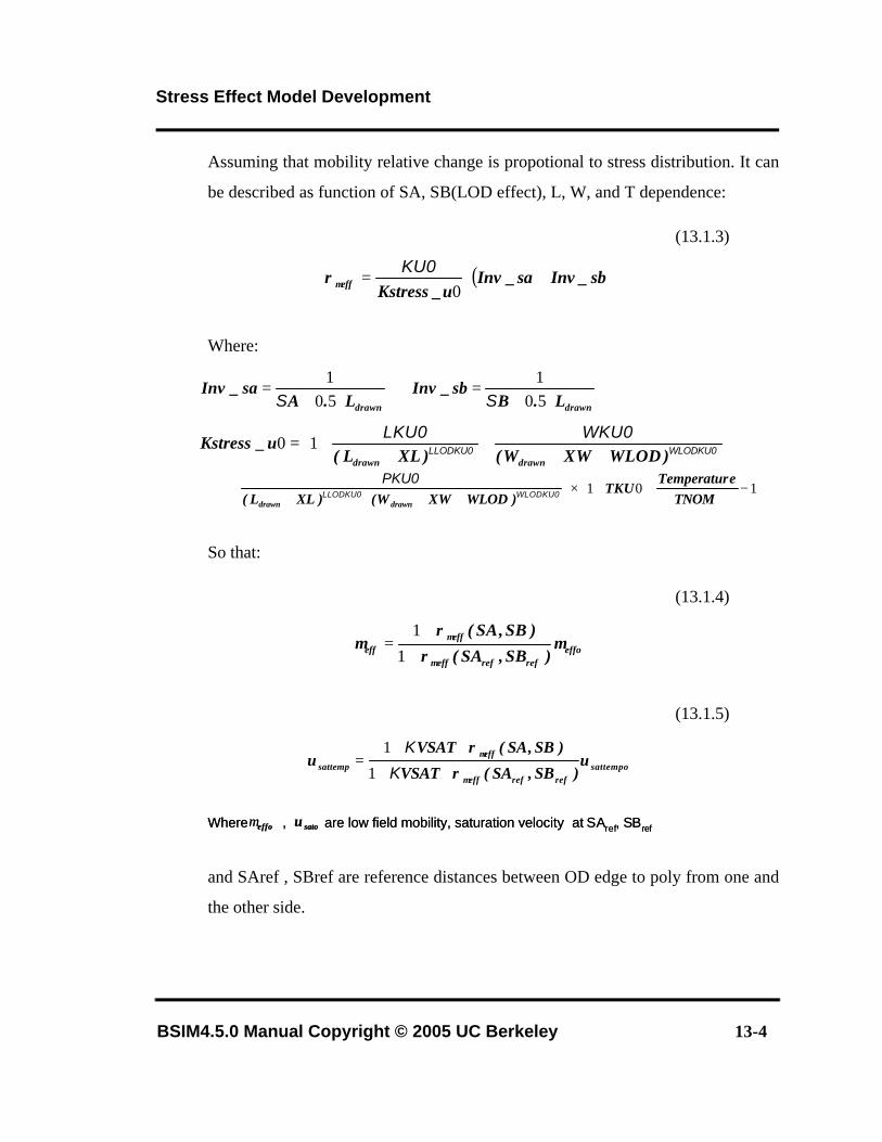
Stress Effect Model Development
BSIM4.5.0 Manual Copyright © 2005 UC Berkeley 13-4
Assuming that mobility relative change is propotional to stress distribution. It can
be described as function of SA, SB(LOD effect), L, W, and T dependence:
(13.1.3)
Where:
So that:
(13.1.4)
(13.1.5)
and SAref , SBref are reference distances between OD edge to poly from one and
the other side.
( )sb_Invsa_Invu_Kstresseff +⋅=
0KU0
µρ
drawnL.Asa_Inv
⋅+=
501
S
++
++
+= WLODKU0LLODKU0
WKU0LKU0)WLODXWW()XLL(
u_Kstressdrawndrawn
10
−⋅+×
++⋅+
+ 101TNOM
eTemperaturTKU
)WLODXWW()XLL( drawndrawnWLODKU0LLODKU0
PKU0
drawnL.Bsb_Inv
⋅+=
501
S
efforefrefeff
effeff )SB,SA(
)SB,SA(µ
ρρ
µµ
µ
++
=1
1
sattemporefrefeff
effsattemp )SB,SA(VSAT
)SB,SA(VSATυ
ρ
ρυ
µ
µ
⋅+
⋅+=
K
K
1
1
Where , are low field mobility, saturation velocity at SAref, SBrefeffoµ satoυWhere , are low field mobility, saturation velocity at SAref, SBrefeffoµ satoυ
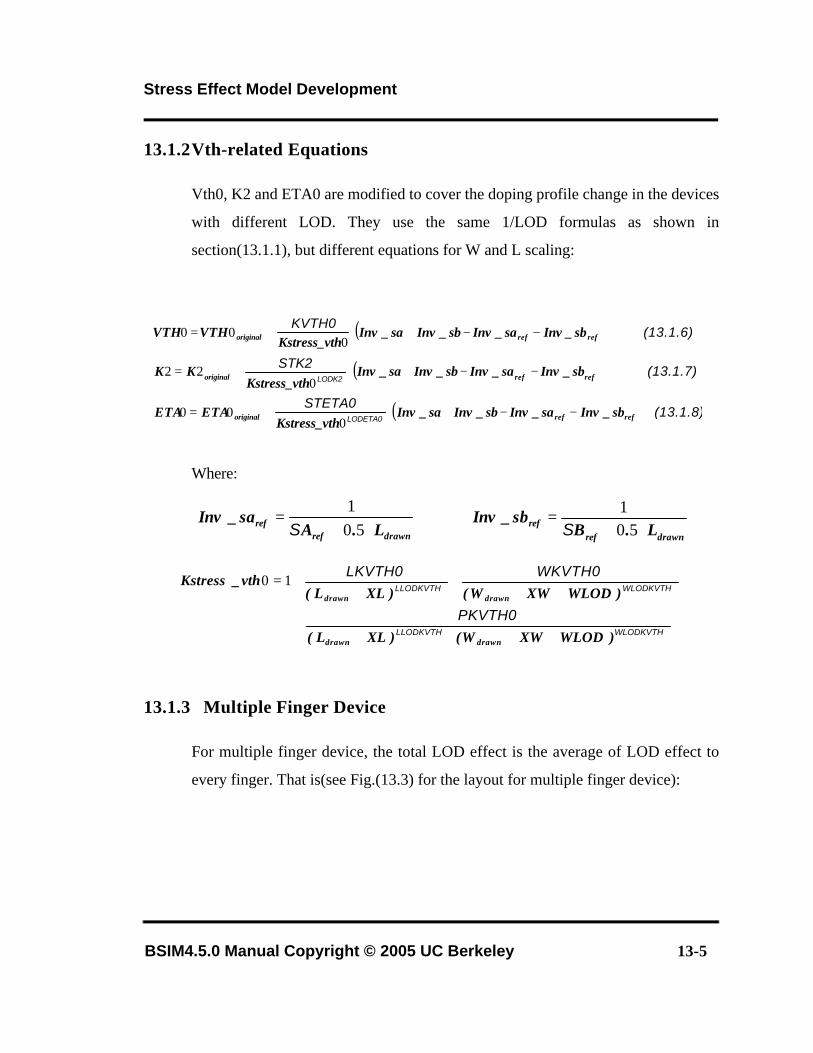
Stress Effect Model Development
BSIM4.5.0 Manual Copyright © 2005 UC Berkeley 13-5
13.1.2Vth-related Equations
Vth0, K2 and ETA0 are modified to cover the doping profile change in the devices
with different LOD. They use the same 1/LOD formulas as shown in
section(13.1.1), but different equations for W and L scaling:
Where:
13.1.3 Multiple Finger Device
For multiple finger device, the total LOD effect is the average of LOD effect to
every finger. That is(see Fig.(13.3) for the layout for multiple finger device):
( )
( )
( ) (13.1.8) STETA0
(13.1.7) STK2
(13.1.6) KVTH0
LODETA0
LODK2
refreforiginal
refreforiginal
refreforiginal
sb_Invsa_Invsb_Invsa_InvhKstress_vt
ETAETA
sb_Invsa_Invsb_Invsa_InvhKstress_vt
KK
sb_Invsa_Invsb_Invsa_InvhKstress_vt
VTHVTH
−−+⋅+=
−−+⋅+=
−−+⋅+=
000
022
000
drawnrefref L.A
sa_Inv⋅+
=50
1S drawnref
ref L.Bsb_Inv
⋅+=
501
S
WLODKVTHLLODKVTH
WLODKVTHLLODKVTH
PKVTH0
WKVTH0LKVTH0
)WLODXWW()XLL(
)WLODXWW()XLL(vth_Kstress
drawndrawn
drawndrawn
++⋅++
+++
++= 10
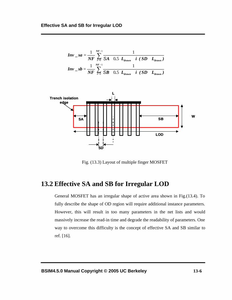
Effective SA and SB for Irregular LOD
BSIM4.5.0 Manual Copyright © 2005 UC Berkeley 13-6
Fig. (13.3) Layout of multiple finger MOSFET
13.2 Effective SA and SB for Irregular LOD
General MOSFET has an irregular shape of active area shown in Fig.(13.4). To
fully describe the shape of OD region will require additional instance parameters.
However, this will result in too many parameters in the net lists and would
massively increase the read-in time and degrade the readability of parameters. One
way to overcome this difficulty is the concept of effective SA and SB similar to
ref. [16].
∑
∑−
=
−
=
+⋅+⋅+=
+⋅+⋅+=
1
0
1
0
5011
5011
NF
i drawndrawn
NF
i drawndrawn
)LSD(iL.BNFsb_Inv
)LSD(iL.ANFsa_Inv
S
S
W
LTrench isolation
edge
SA SB
LOD
SD
W
LTrench isolation
edge
SA SB
LOD
SD
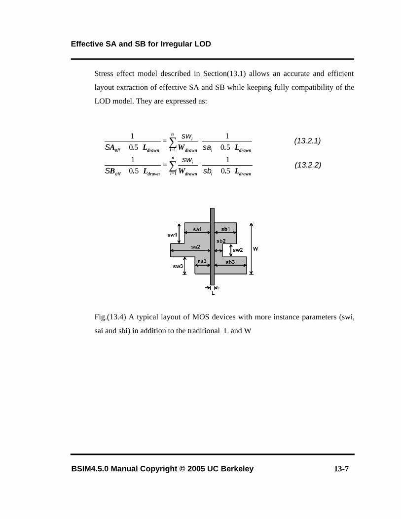
Effective SA and SB for Irregular LOD
BSIM4.5.0 Manual Copyright © 2005 UC Berkeley 13-7
Stress effect model described in Section(13.1) allows an accurate and efficient
layout extraction of effective SA and SB while keeping fully compatibility of the
LOD model. They are expressed as:
Fig.(13.4) A typical layout of MOS devices with more instance parameters (swi,
sai and sbi) in addition to the traditional L and W
(13.2.2) sb
swS
(13.2.1) sa
swS
i
i
eff
i
i
eff
∑
∑
=
=
⋅+⋅=
⋅+
⋅+⋅=
⋅+n
i drawndrawndrawn
n
i drawndrawndrawn
L.WL.B
L.WL.A
1
1
501
501
501
501
BSIM4.5.0 Manual Copyright © 2005 UC Berkeley 14-1
Chapter 14: Well Proximity Effect Model
Retrograde well profiles have several key advantages for highly scaled bulk
complementary metal oxide semiconductor(CMOS) technology. With the advent of
high-energy implanters and reduced thermal cycle processing, it has become
possible to provide a relatively heavily doped deep nwell and pwell without
affecting the critical device-related doping at the surface. The deep well implants
provide a low resistance path and suppress parasitic bipolar gain for latchup
protection, and can also improve soft error rate and noise isolation. A deep buried
layer is also key to forming triple-well structures for isolated-well NMOSFETs.
However, deep buried layers can affect devices located near the mask edge. Some of
the ions scattered out of the edge of the photoresist are implanted in the silicon
surface near the mask edge, altering the threshold voltage of those devices[17]. It is
observed a threshold voltage shifts of up to 100 mV in a deep boron retrograde
pwell, a deep phosphorus retrograde nwell, and also a triple-well implementation
with a deep phosphorus isolation layer below the pwell over a lateral distance on the
order of a micrometer[17]. This effect is called well proximity effect.
BSIM4 considers the influence of well proximity effect on threshold voltage,
mobility, and body effect. This well proximity effect model is developed by
Compact Model Council[18].
Well Proximity Effect Model
14-2 BSIM4.5.0 Manual Copyright © 2005 UC Berkeley
14.1 Well Proximity Effect Model
Experimental analysis[17] shows that well proximity effect is strong function of
distance of FET from mask edge, and electrical quantities influenced by it follow the
same geometrical trend. A phenomenological model based on these findings has
been developed by modifying some parameters in the BSIM model. Note that the
following equations have no impact on the iteration time because there are no
voltage-controlled components in them.
14.1.1 Equations for Threshold Voltage, Body Effect, and Mobility
Due to the well proximity effect, their new equations can be described as:
(14.1.1)
where SCA, SCB, SCC are instance parameters that represent the integral of the
first/second/third distribution function for scattered well dopant.
( )
( )
( )( )SCCWECSCBWEBSCAKU0WE1
SCCWECSCBWEBSCAK2WE22
SCCWECSCBWEBSCAKVTH0WE00
, ⋅+⋅+⋅+⋅=
⋅+⋅+⋅+=
⋅+⋅+⋅+=
orgeffeff
org
org
KK
VthVth
µµ
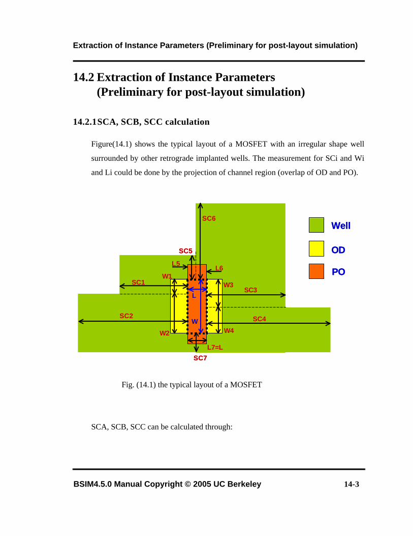
Extraction of Instance Parameters (Preliminary for post-layout simulation)
BSIM4.5.0 Manual Copyright © 2005 UC Berkeley 14-3
14.2 Extraction of Instance Parameters (Preliminary for post-layout simulation)
14.2.1SCA, SCB, SCC calculation
Figure(14.1) shows the typical layout of a MOSFET with an irregular shape well
surrounded by other retrograde implanted wells. The measurement for SCi and Wi
and Li could be done by the projection of channel region (overlap of OD and PO).
Fig. (14.1) the typical layout of a MOSFET
SCA, SCB, SCC can be calculated through:
L
W
Well
OD
POW1SC1
SC2
W2
SC7
L7=L
W3
W4
SC3
SC4
L5L6
SC5
SC6
L
W
Well
OD
POW1SC1
SC2
W2
SC7
L7=L
W3
W4
SC3
SC4
L5L6
SC5
SC6
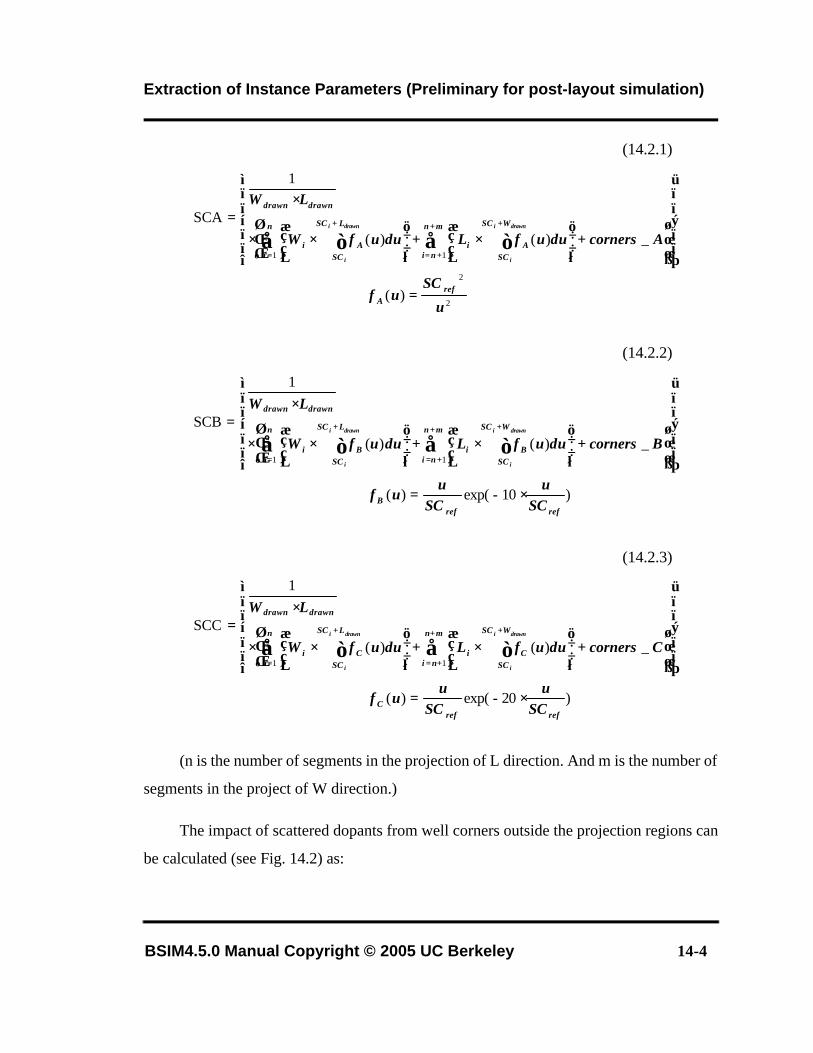
Extraction of Instance Parameters (Preliminary for post-layout simulation)
BSIM4.5.0 Manual Copyright © 2005 UC Berkeley 14-4
(14.2.1)
(14.2.2)
(14.2.3)
(n is the number of segments in the projection of L direction. And m is the number of
segments in the project of W direction.)
The impact of scattered dopants from well corners outside the projection regions can
be calculated (see Fig. 14.2) as:
2
2
11
)(
_)()(
1
SCA
u
SCuf
AcornersduufLduufW
LW
refA
mn
ni
WSC
SCAi
n
i
LSC
SCAi
drawndrawn
drawni
i
drawni
i
=
+
⋅+
⋅⋅
⋅=
∑ ∫∑ ∫+
+=
+
=
+
)10exp()(
_)()(
1
SCB
11
refrefB
mn
ni
WSC
SCBi
n
i
LSC
SCBi
drawndrawn
SCu
SCu
uf
BcornersduufLduufW
LW
drawni
i
drawni
i
⋅−=
+
⋅+
⋅⋅
⋅=
∑ ∫∑ ∫+
+=
+
=
+
)20exp()(
_)()(
1
SCC
11
refrefC
mn
ni
WSC
SCCi
n
i
LSC
SCCi
drawndrawn
SCu
SCu
uf
CcornersduufLduufW
LW
drawni
i
drawni
i
⋅−=
+
⋅+
⋅⋅
⋅=
∑ ∫∑ ∫+
+=
+
=
+
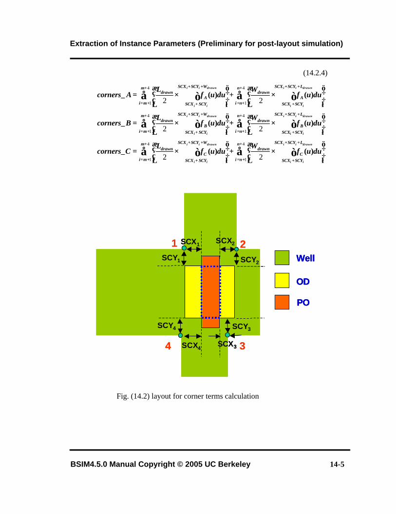
Extraction of Instance Parameters (Preliminary for post-layout simulation)
BSIM4.5.0 Manual Copyright © 2005 UC Berkeley 14-5
(14.2.4)
Fig. (14.2) layout for corner terms calculation
∑ ∫∑ ∫
∑ ∫∑ ∫
∑ ∫∑ ∫
+
+=
++
+
+
+=
++
+
+
+=
++
+
+
+=
++
+
+
+=
++
+
+
+=
++
+
⋅+
⋅=
⋅+
⋅=
⋅+
⋅=
4
1
4
1
4
1
4
1
4
1
4
1
22
22
22
n
ni
LSCYSCX
SCYSCXC
drawnm
mi
WSCYSCX
SCYSCXC
drawn
n
ni
LSCYSCX
SCYSCXB
drawnm
mi
WSCYSCX
SCYSCXB
drawn
n
ni
LSCYSCX
SCYSCXA
drawnm
mi
WSCYSCX
SCYSCXA
drawn
drawnii
ii
drawnii
ii
drawnii
ii
drawnii
ii
drawnii
ii
drawnii
ii
duufW
duufL
Ccorners
duufW
duufL
Bcorners
duufW
duufL
Acorners
)()(_
)()(_
)()(_
Well
OD
PO
SCY1
SCX11 2
34
SCX2
SCY2
SCY3
SCX3SCX4
SCY4
Well
OD
PO
Well
OD
PO
SCY1
SCX11 2
34
SCX2
SCY2
SCY3
SCX3SCX4
SCY4
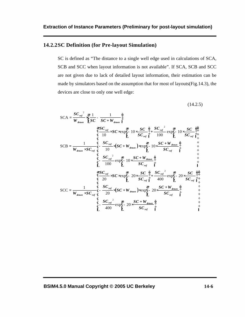
Extraction of Instance Parameters (Preliminary for post-layout simulation)
BSIM4.5.0 Manual Copyright © 2005 UC Berkeley 14-6
14.2.2SC Definition (for Pre-layout Simulation)
SC is defined as “The distance to a single well edge used in calculations of SCA,
SCB and SCC when layout information is not available”. If SCA, SCB and SCC
are not given due to lack of detailed layout information, their estimation can be
made by simulators based on the assumption that for most of layouts(Fig.14.3), the
devices are close to only one well edge:
(14.2.5)
( )
( )
+⋅−−
+⋅−⋅+⋅−
⋅−+
⋅−⋅⋅
⋅=
+⋅−−
+⋅−⋅+⋅−
⋅−+
⋅−⋅⋅
⋅=
+
−⋅=
ref
drawnref
ref
drawndrawn
ref
ref
ref
ref
ref
refdrawn
ref
drawnref
ref
drawndrawn
ref
ref
ref
ref
ref
refdrawn
drawndrawn
ref
SC
WSCSC
SCWSC
WSCSC
SCSCSC
SCSC
SCSC
SCW
SCWSCSC
SCWSC
WSCSC
SCSCSC
SCSCSC
SC
SCW
WSCSCW
SC
20exp400
20exp20
20exp400
20exp20
1SCC
10exp100
10exp10
10exp100
10exp10
1SCB
11SCA
2
2
2
2
2
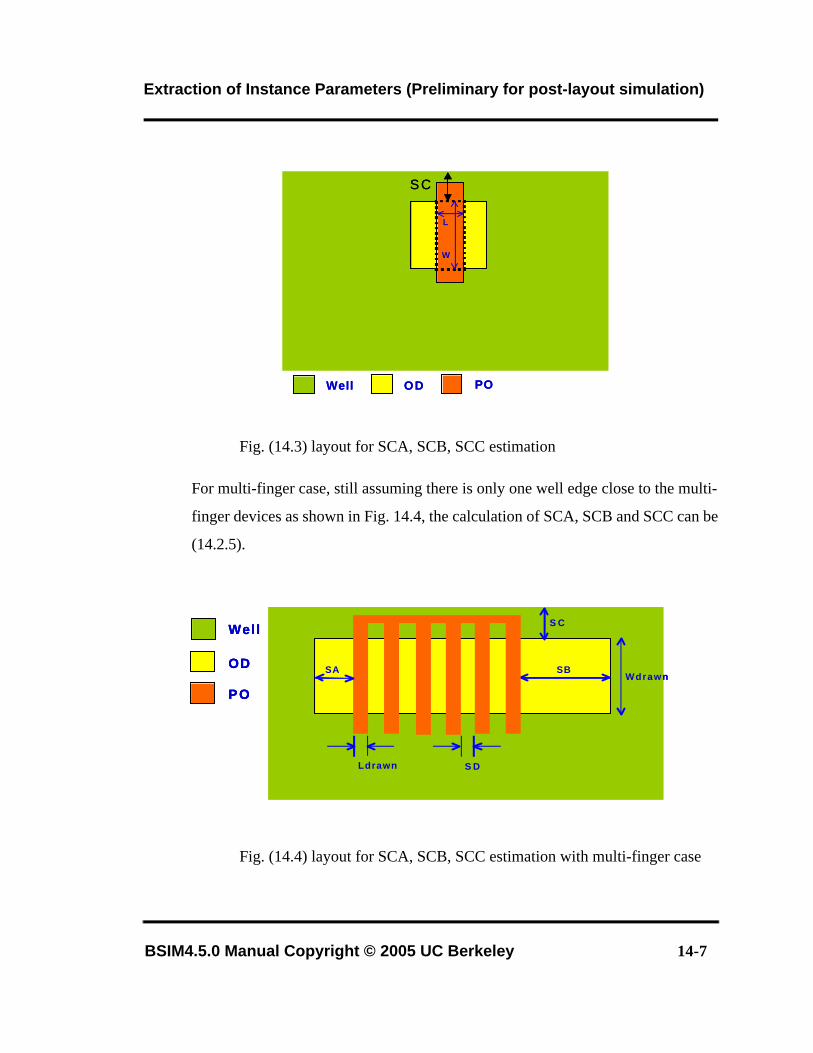
Extraction of Instance Parameters (Preliminary for post-layout simulation)
BSIM4.5.0 Manual Copyright © 2005 UC Berkeley 14-7
Fig. (14.3) layout for SCA, SCB, SCC estimation
For multi-finger case, still assuming there is only one well edge close to the multi-
finger devices as shown in Fig. 14.4, the calculation of SCA, SCB and SCC can be
(14.2.5).
Fig. (14.4) layout for SCA, SCB, SCC estimation with multi-finger case
Well OD POWell OD PO
L
W
S C
L
W
L
W
S C
Well
OD
PO
Ldrawn
WdrawnSBSA
S C
S D
Well
OD
PO
Well
OD
PO
Ldrawn
WdrawnSBSA
S C
S D
BSIM4.5.0 Manual Copyright © 2005 UC Berkeley 15-1
CHAPTER 15: Parameter Extraction Methodology
Parameter extraction is an important part of model development. The extraction
methodology depends on the model and on the way the model is used. A combination of a
local optimization and the group device extraction strategy is adopted for parameter
extraction.
15.1 Optimization strategy
There are two main, different optimization strategies: global optimization and
local optimization. Global optimization relies on the explicit use of a computer to
find one set of model parameters which will best fit the available experimental
(measured) data. This methodology may give the minimum average error between
measured and simulated (calculated) data points, but it also treats each parameter
as a "fitting" parameter. Physical parameters extracted in such a manner might
yield values that are not consistent with their physical intent.
In local optimization, many parameters are extracted independently of one
another. Parameters are extracted from device bias conditions which correspond to
dominant physical mechanisms. Parameters which are extracted in this manner
might not fit experimental data in all the bias conditions. Nonetheless, these
extraction methodologies are developed specifically with respect to a given
parameter’s physical meaning. If properly executed, it should, overall, predict
Extraction Strategy
15-2 BSIM4.5.0 Manual Copyright © 2005 UC Berkeley
device performance quite well. Values extracted in this manner will now have
some physical relevance.
15.2 Extraction Strategy
Two different strategies are available for extracting parameters: single device
extraction strategy and group device extraction strategy. In single device
extraction strategy, experimental data from a single device is used to extract a
complete set of model parameters. This strategy will fit one device very well but
will not fit other devices with different geometries. Furthermore, single device
extraction strategy can not guarantee that the extracted parameters are physical. If
only one set of channel length and width is used, parameters related to channel
length and channel width dependencies can not be determined.
It is suggested that BSIM4 use group device extraction strategy. This requires
measured data from devices with different geometries. All devices are measured
under the same bias conditions. The resulting fit might not be absolutely perfect
for any single device but will be better for the group of devices under
consideration. In the following, a general extraction methodology is proposed for
basic BSIM4 model parameters. Thus, it will not cover other model parameters,
such as those of the gate tunneling current model and RF models, etc.
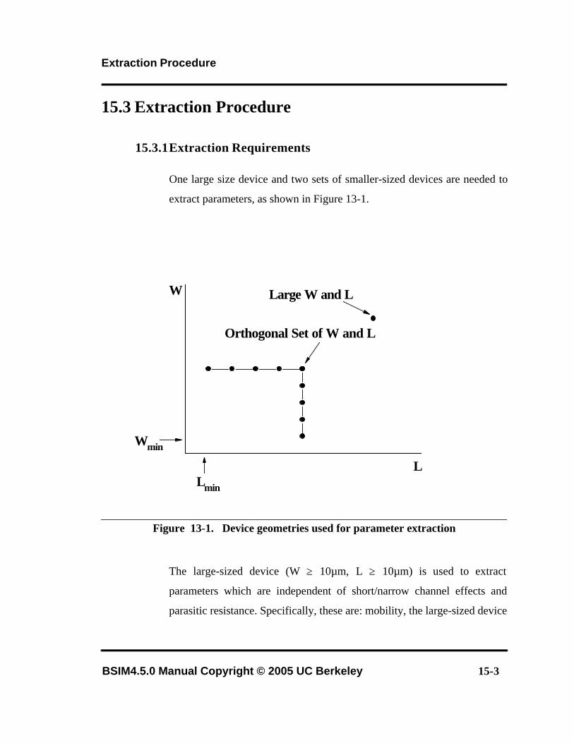
Extraction Procedure
BSIM4.5.0 Manual Copyright © 2005 UC Berkeley 15-3
15.3 Extraction Procedure
15.3.1Extraction Requirements
One large size device and two sets of smaller-sized devices are needed to
extract parameters, as shown in Figure 13-1.
Figure 13-1. Device geometries used for parameter extraction
The large-sized device (W ≥ 10µm, L ≥ 10µm) is used to extract
parameters which are independent of short/narrow channel effects and
parasitic resistance. Specifically, these are: mobility, the large-sized device
Orthogonal Set of W and L
Wmin
Lmin
Large W and LW
L
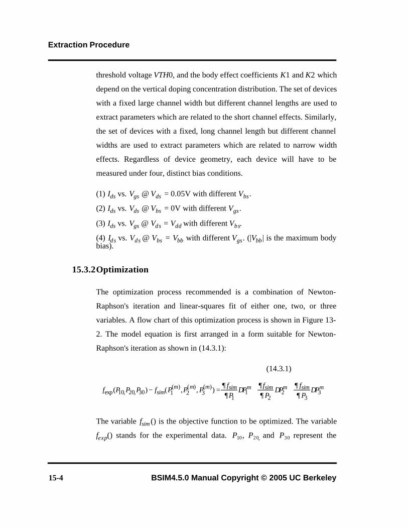
Extraction Procedure
15-4 BSIM4.5.0 Manual Copyright © 2005 UC Berkeley
threshold voltage VTH0, and the body effect coefficients K1 and K2 which
depend on the vertical doping concentration distribution. The set of devices
with a fixed large channel width but different channel lengths are used to
extract parameters which are related to the short channel effects. Similarly,
the set of devices with a fixed, long channel length but different channel
widths are used to extract parameters which are related to narrow width
effects. Regardless of device geometry, each device will have to be
measured under four, distinct bias conditions.
(1) Ids vs. Vgs @ Vds = 0.05V with different Vbs.
(2) Ids vs. Vds @ Vbs = 0V with different Vgs.
(3) Ids vs. Vgs @ Vds = Vdd with different Vbs.
(4) Ids vs. Vds @ Vbs = Vbb with different Vgs. (|Vbb | is the maximum bodybias).
15.3.2Optimization
The optimization process recommended is a combination of Newton-
Raphson's iteration and linear-squares fit of either one, two, or three
variables. A flow chart of this optimization process is shown in Figure 13-
2. The model equation is first arranged in a form suitable for Newton-
Raphson's iteration as shown in (14.3.1):
(14.3.1)
The variable fsim () is the objective function to be optimized. The variable
fexp() stands for the experimental data. P10, P20, and P30 represent the
f P P P f P P PfP
PfP
PfP
Psimm m m sim m sim m sim m
exp , ,( ) ( ) ( )( ) ( , , )10 20 30 1 2 3
11
22
33− = + +
∂∂
∂∂
∂∂
∆ ∆ ∆
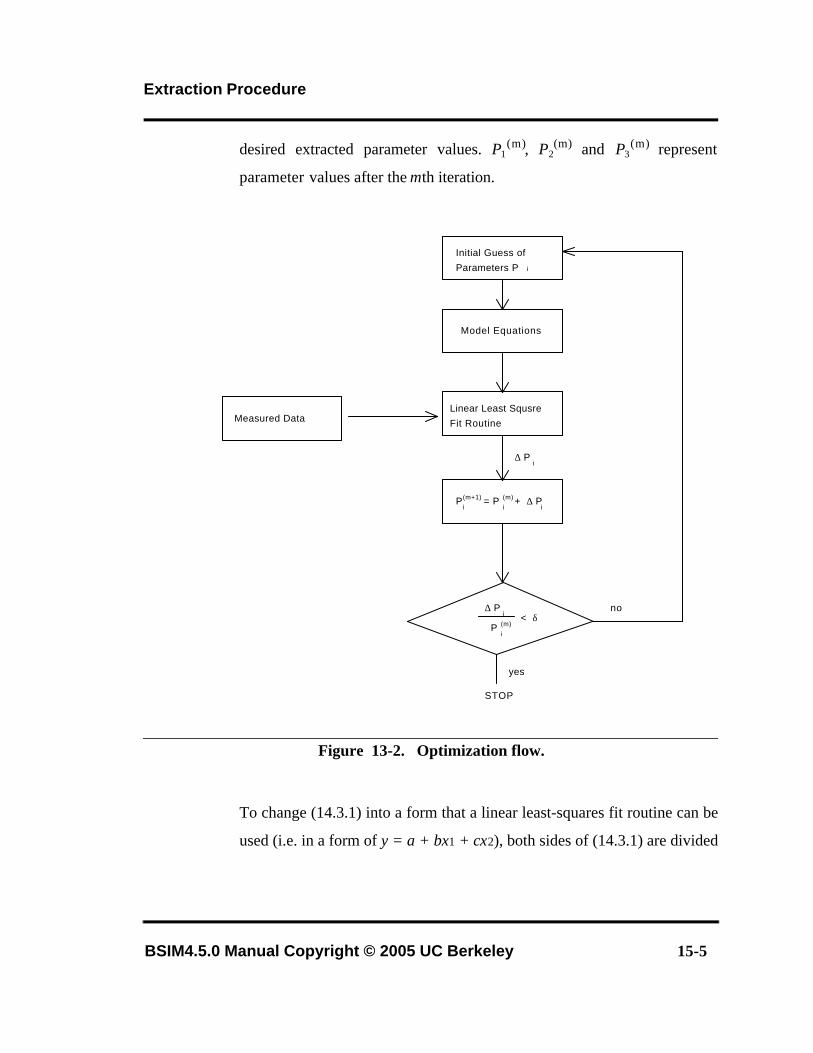
Extraction Procedure
BSIM4.5.0 Manual Copyright © 2005 UC Berkeley 15-5
desired extracted parameter values. P1(m), P2
(m) and P3(m) represent
parameter values after the mth iteration.
Figure 13-2. Optimization flow.
To change (14.3.1) into a form that a linear least-squares fit routine can be
used (i.e. in a form of y = a + bx1 + cx2), both sides of (14.3.1) are divided
Initial Guess of
Parameters P i
Model Equations
Linear Least Squsre
Fit Routine
P = P + ∆ P i i i
(m+1) (m)
Measured Data
STOP
yes
no
∆ Pi
∆ Pi
P i
(m)< δ
Extraction Procedure
15-6 BSIM4.5.0 Manual Copyright © 2005 UC Berkeley
by ∂fsim / ∂P1. This gives the change in P1, ∆P1(m) , for the next iteration
such that:
(14.3.2)
where i=1, 2, 3 for this example. The (m+1) parameter values for P2 and P3
are obtained in an identical fashion. This process is repeated until the
incremental parameter change in parameter values ∆Pi(m) are smaller than
a pre-determined value. At this point, the parameters P1, P2, and P3 have
been extracted.
15.3.3Extraction Routine
Before any model parameters can be extracted, some process parameters
have to be provided. They are listed below in Table 13-1:
Table 13-1. Prerequisite input parameters prior to extraction process.
Input Parameters Names Physical Meaning
TOXE, TOXP, DTOX, or EPSROX
Gate oxide thickness and dielectric con-stant
NDEP Doping concentration in the channel
TNOM Temperature at which the data is taken
Ldrawn Mask level channel length
Wdrawn Mask level channel width
XJ Junction depth
P P Pim
im
im( ) ( ) ( )+ = +1 ∆
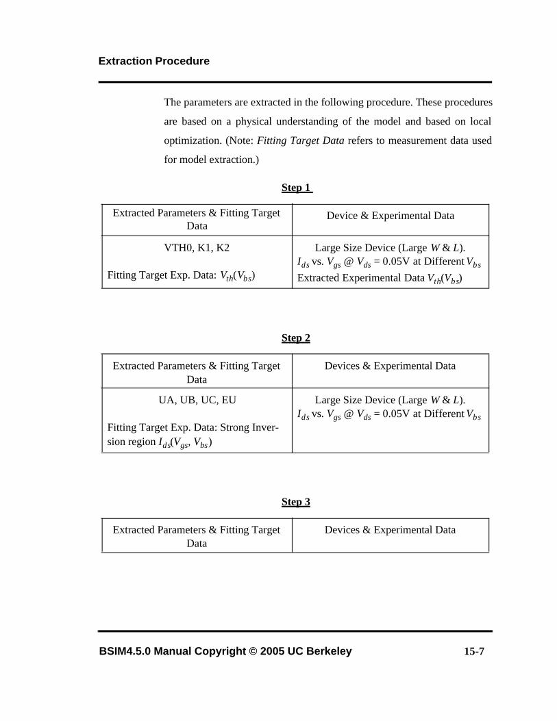
Extraction Procedure
BSIM4.5.0 Manual Copyright © 2005 UC Berkeley 15-7
The parameters are extracted in the following procedure. These procedures
are based on a physical understanding of the model and based on local
optimization. (Note: Fitting Target Data refers to measurement data used
for model extraction.)
Step 1
Step 2
Step 3
Extracted Parameters & Fitting Target Data
Device & Experimental Data
VTH0, K1, K2
Fitting Target Exp. Data: Vth(Vbs)
Large Size Device (Large W & L). Ids vs. Vgs @ Vds = 0.05V at Different Vbs
Extracted Experimental Data Vth(Vbs)
Extracted Parameters & Fitting Target Data
Devices & Experimental Data
UA, UB, UC, EU
Fitting Target Exp. Data: Strong Inver-sion region Ids(Vgs, Vbs)
Large Size Device (Large W & L). Ids vs. Vgs @ Vds = 0.05V at Different Vbs
Extracted Parameters & Fitting Target Data
Devices & Experimental Data
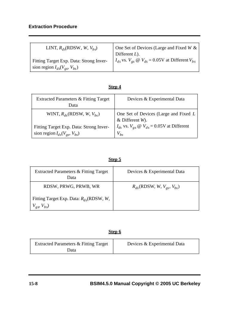
Extraction Procedure
15-8 BSIM4.5.0 Manual Copyright © 2005 UC Berkeley
Step 4
Step 5
Step 6
LINT, Rds(RDSW, W, Vbs)
Fitting Target Exp. Data: Strong Inver-sion region Ids(Vgs, Vbs)
One Set of Devices (Large and Fixed W &Different L). Ids vs. Vgs @ Vds = 0.05V at Different Vbs
Extracted Parameters & Fitting Target Data
Devices & Experimental Data
WINT, Rds(RDSW, W, Vbs)
Fitting Target Exp. Data: Strong Inver-sion region Ids(Vgs, Vbs)
One Set of Devices (Large and Fixed L& Different W). Ids vs. Vgs @ Vds = 0.05V at Different Vbs
Extracted Parameters & Fitting Target Data
Devices & Experimental Data
RDSW, PRWG, PRWB, WR
Fitting Target Exp. Data: Rds(RDSW, W, Vgs, Vbs)
Rds(RDSW, W, Vgs, Vbs)
Extracted Parameters & Fitting Target Data
Devices & Experimental Data
Extraction Procedure
BSIM4.5.0 Manual Copyright © 2005 UC Berkeley 15-9
Step 7
Step 8
Step 9
DVT0, DVT1, DVT2, LPE0, LPEB
Fitting Target Exp. Data: Vth(Vbs, L, W)
One Set of Devices (Large and Fixed W &Different L).
Vth(Vbs, L, W)
Extracted Parameters & Fitting Target Data
Devices & Experimental Data
DVT0W, DVT1W, DVT2WFitting Target Exp. Data: Vth(Vbs, L, W)
One Set of Devices (Large and Fixed L &Different W).
Vth(Vbs, L, W)
Extracted Parameters & Fitting Target Data
Devices & Experimental Data
K3, K3B, W0
Fitting Target Exp. Data: Vth(Vbs, L, W)
One Set of Devices (Large and Fixed L &Different W).
Vth(Vbs, L, W)
Extracted Parameters & Fitting Target Data
Devices & Experimental Data
MINV, VOFF, VOFFL, NFACTOR, CDSC, CDSCB
Fitting Target Exp. Data: Subthreshold region Ids(Vgs, Vbs)
One Set of Devices (Large and Fixed W &Different L). Ids vs. Vgs @ Vds = 0.05V at Different Vbs
Extraction Procedure
15-10 BSIM4.5.0 Manual Copyright © 2005 UC Berkeley
Step 10
Step 11
Step 12
Extracted Parameters & Fitting Target Data
Devices & Experimental Data
CDSCDFitting Target Exp. Data: Subthreshold region Ids(Vgs, Vbs)
One Set of Devices (Large and Fixed W &Different L). Ids vs. Vgs @ Vbs = Vbb at Different Vds
Extracted Parameters & Fitting Target Data
Devices & Experimental Data
DWBFitting Target Exp. Data: Strong Inver-sion region Ids(Vgs, Vbs)
One Set of Devices (Large and Fixed W &Different L). Ids vs. Vgs @ Vds = 0.05V at Different Vbs
Extracted Parameters & Fitting Target Data
Devices & Experimental Data
VSAT, A0, AGS, LAMBDA, XN, VTL, LC
Fitting Target Exp. Data: Isat(Vgs, Vbs)/WA1, A2 (PMOS Only)
Fitting Target Exp. Data Vdsat(Vgs)
One Set of Devices (Large and Fixed W &Different L). Ids vs. Vds @ Vbs = 0V at Different Vgs
Extraction Procedure
BSIM4.5.0 Manual Copyright © 2005 UC Berkeley 15-11
Step 13
Step 14
Step 15
Step 16
Extracted Parameters & Fitting Target Data
Devices & Experimental Data
B0, B1Fitting Target Exp. Data: Isat(Vgs, Vbs)/W
One Set of Devices (Large and Fixed L &Different W). Ids vs. Vds @ Vbs = 0V at Different Vgs
Extracted Parameters & Fitting Target Data
Devices & Experimental Data
DWGFitting Target Exp. Data: Isat(Vgs, Vbs)/W
One Set of Devices (Large and Fixed L &Different W). Ids vs. Vds @ Vbs = 0V at Different Vgs
Extracted Parameters & Fitting Target Data
Devices & Experimental Data
PSCBE1, PSCBE2
Fitting Target Exp. Data: Rout(Vgs, Vds)
One Set of Devices (Large and Fixed W &Different L). Ids vs. Vds @ Vbs = 0V at Different Vgs
Extracted Parameters & Fitting Target Data
Devices & Experimental Data
Extraction Procedure
15-12 BSIM4.5.0 Manual Copyright © 2005 UC Berkeley
Step 17
Step 18
Step 19
PCLM, θ(DROUT, PDIBLC1, PDIBLC2, L), PVAG, FPROUT, DITS,
DITSL, DITSDFitting Target Exp. Data: Rout(Vgs, Vds)
One Set of Devices (Large and Fixed W &Different L). Ids vs. Vds @ Vbs = 0V at Different Vgs
Extracted Parameters & Fitting Target Data
Devices & Experimental Data
DROUT, PDIBLC1, PDIBLC2Fitting Target Exp. Data: θ(DROUT, PDIBLC1, PDIBLC2, L)
One Set of Devices (Large and Fixed W &Different L). θ(DROUT, PDIBLC1, PDIBLC2, L)
Extracted Parameters & Fitting Target Data
Devices & Experimental Data
PDIBLCB
Fitting Target Exp. Data: θ(DROUT, PDIBLC1, PDIBLC2, L, Vbs)
One Set of Devices (Large and Fixed W &Different L). Ids vs. Vgs @ fixed Vgs at Different Vbs
Extracted Parameters & Fitting Target Data
Devices & Experimental Data
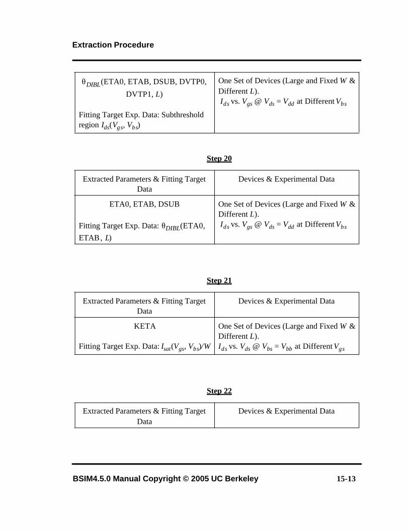
Extraction Procedure
BSIM4.5.0 Manual Copyright © 2005 UC Berkeley 15-13
Step 20
Step 21
Step 22
θDIBL(ETA0, ETAB, DSUB, DVTP0,
DVTP1, L)
Fitting Target Exp. Data: Subthreshold region Ids(Vgs, Vbs)
One Set of Devices (Large and Fixed W &Different L). Ids vs. Vgs @ Vds = Vdd at Different Vbs
Extracted Parameters & Fitting Target Data
Devices & Experimental Data
ETA0, ETAB, DSUB
Fitting Target Exp. Data: θDIBL(ETA0, ETAB , L)
One Set of Devices (Large and Fixed W &Different L). Ids vs. Vgs @ Vds = Vdd at Different Vbs
Extracted Parameters & Fitting Target Data
Devices & Experimental Data
KETA
Fitting Target Exp. Data: Isat(Vgs, Vbs)/W
One Set of Devices (Large and Fixed W &Different L). Ids vs. Vds @ Vbs = Vbb at Different Vgs
Extracted Parameters & Fitting Target Data
Devices & Experimental Data
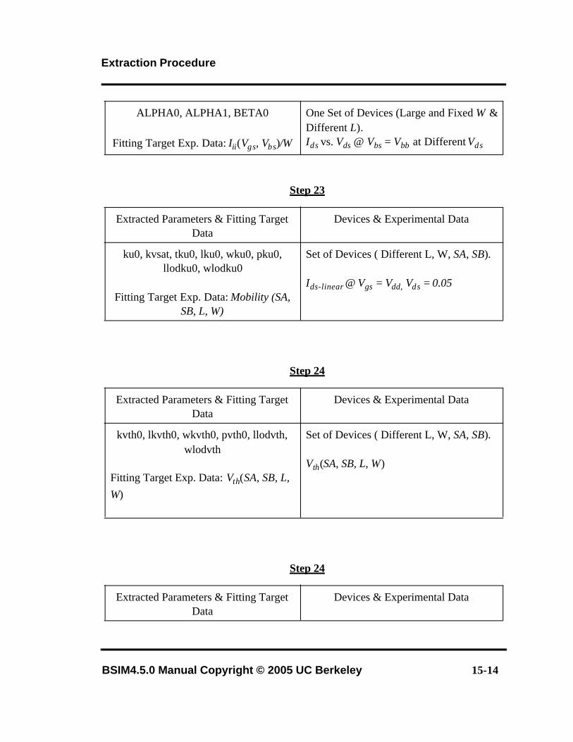
Extraction Procedure
BSIM4.5.0 Manual Copyright © 2005 UC Berkeley 15-14
Step 23
Step 24
Step 24
ALPHA0, ALPHA1, BETA0
Fitting Target Exp. Data: Iii(Vgs, Vbs)/W
One Set of Devices (Large and Fixed W &Different L). Ids vs. Vds @ Vbs = Vbb at Different Vds
Extracted Parameters & Fitting Target Data
Devices & Experimental Data
ku0, kvsat, tku0, lku0, wku0, pku0, llodku0, wlodku0
Fitting Target Exp. Data: Mobility (SA, SB, L, W)
Set of Devices ( Different L, W, SA, SB).
Ids-linear @ Vgs = Vdd, Vds = 0.05
Extracted Parameters & Fitting Target Data
Devices & Experimental Data
kvth0, lkvth0, wkvth0, pvth0, llodvth, wlodvth
Fitting Target Exp. Data: Vth(SA, SB, L, W)
Set of Devices ( Different L, W, SA, SB).
Vth(SA, SB, L, W)
Extracted Parameters & Fitting Target Data
Devices & Experimental Data
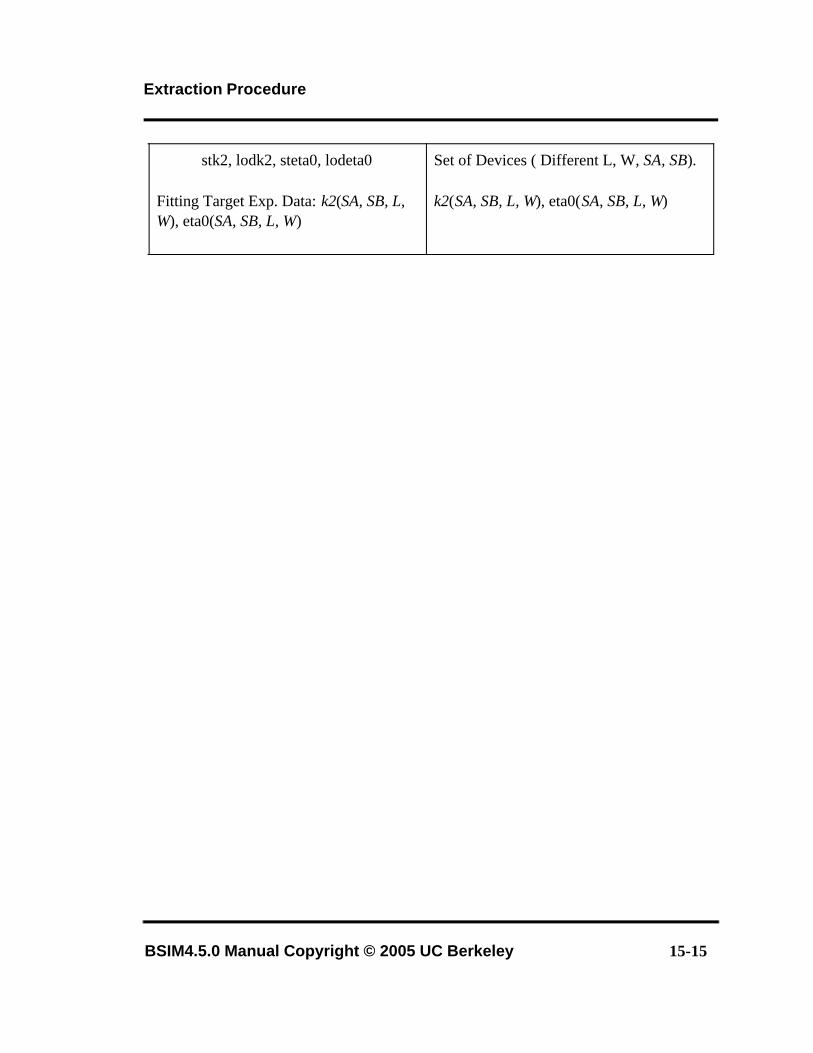
Extraction Procedure
BSIM4.5.0 Manual Copyright © 2005 UC Berkeley 15-15
stk2, lodk2, steta0, lodeta0
Fitting Target Exp. Data: k2(SA, SB, L, W), eta0(SA, SB, L, W)
Set of Devices ( Different L, W, SA, SB).
k2(SA, SB, L, W), eta0(SA, SB, L, W)
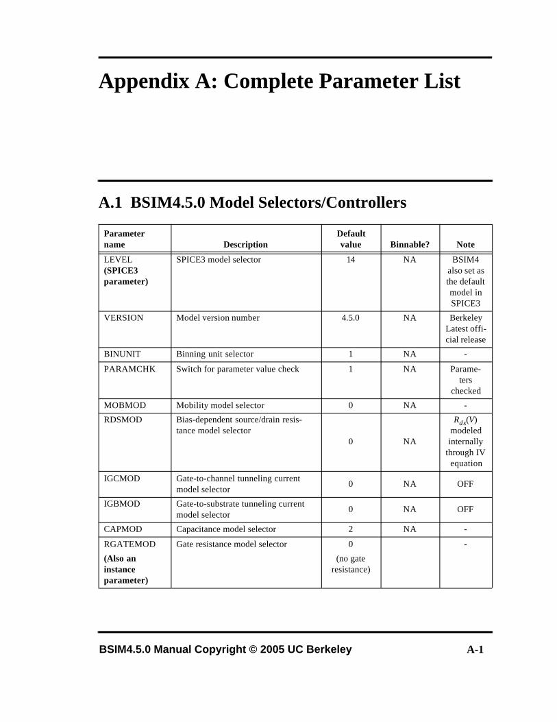
BSIM4.5.0 Manual Copyright © 2005 UC Berkeley A-1
Appendix A: Complete Parameter List
A.1 BSIM4.5.0 Model Selectors/Controllers
Parameter name Description
Default value Binnable? Note
LEVEL (SPICE3 parameter)
SPICE3 model selector 14 NA BSIM4 also set as the default model in SPICE3
VERSION Model version number 4.5.0 NA Berkeley Latest offi-cial release
BINUNIT Binning unit selector 1 NA -
PARAMCHK Switch for parameter value check 1 NA Parame-ters
checked
MOBMOD Mobility model selector 0 NA -
RDSMOD Bias-dependent source/drain resis-tance model selector
0 NA
Rds(V) modeled internally
through IV equation
IGCMOD Gate-to-channel tunneling current model selector
0 NA OFF
IGBMOD Gate-to-substrate tunneling current model selector
0 NA OFF
CAPMOD Capacitance model selector 2 NA -
RGATEMOD
(Also an instance parameter)
Gate resistance model selector 0
(no gate resistance)
-
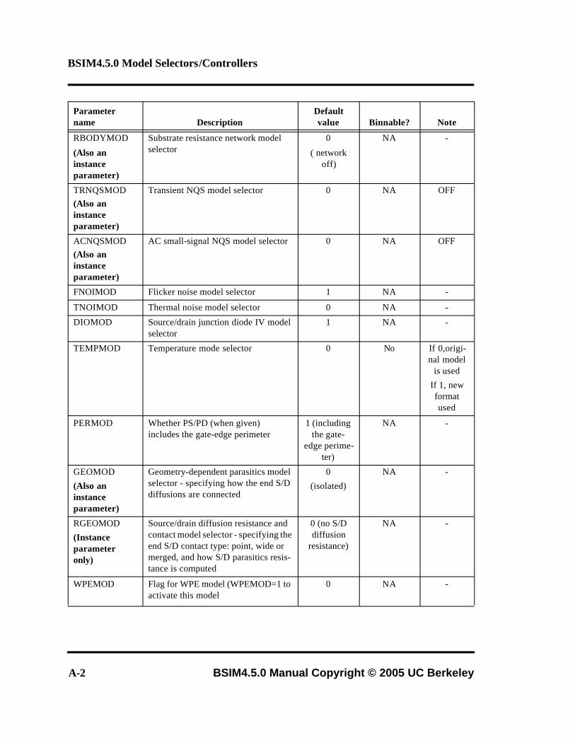
BSIM4.5.0 Model Selectors/Controllers
A-2 BSIM4.5.0 Manual Copyright © 2005 UC Berkeley
RBODYMOD
(Also an instance parameter)
Substrate resistance network model selector
0
( network off)
NA -
TRNQSMOD(Also an instance parameter)
Transient NQS model selector 0 NA OFF
ACNQSMOD(Also an instance parameter)
AC small-signal NQS model selector 0 NA OFF
FNOIMOD Flicker noise model selector 1 NA -
TNOIMOD Thermal noise model selector 0 NA -
DIOMOD Source/drain junction diode IV model selector
1 NA -
TEMPMOD Temperature mode selector 0 No If 0,origi-nal model
is used
If 1, new format used
PERMOD Whether PS/PD (when given) includes the gate-edge perimeter
1 (including the gate-
edge perime-ter)
NA -
GEOMOD
(Also an instance parameter)
Geometry-dependent parasitics model selector - specifying how the end S/D diffusions are connected
0
(isolated)
NA -
RGEOMOD
(Instance parameter only)
Source/drain diffusion resistance and contact model selector - specifying the end S/D contact type: point, wide or merged, and how S/D parasitics resis-tance is computed
0 (no S/D diffusion
resistance)
NA -
WPEMOD Flag for WPE model (WPEMOD=1 to activate this model
0 NA -
Parameter name Description
Default value Binnable? Note
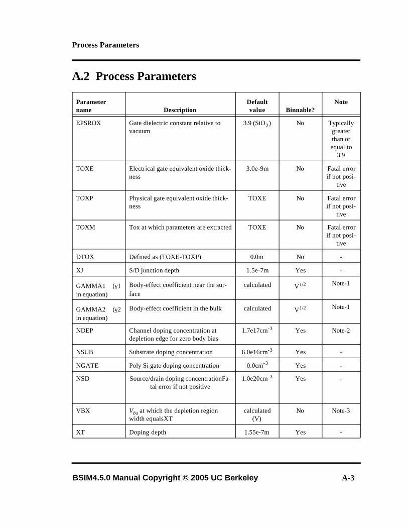
Process Parameters
BSIM4.5.0 Manual Copyright © 2005 UC Berkeley A-3
A.2 Process Parameters
Parameter name Description
Default value Binnable?
Note
EPSROX Gate dielectric constant relative to vacuum
3.9 (SiO2) No Typically greater than or equal to
3.9
TOXE Electrical gate equivalent oxide thick-ness
3.0e-9m No Fatal error if not posi-
tive
TOXP Physical gate equivalent oxide thick-ness
TOXE No Fatal error if not posi-
tive
TOXM Tox at which parameters are extracted TOXE No Fatal error if not posi-
tive
DTOX Defined as (TOXE-TOXP) 0.0m No -
XJ S/D junction depth 1.5e-7m Yes -
GAMMA1 (γ1in equation)
Body-effect coefficient near the sur-face
calculated V1/2 Note-1
GAMMA2 (γ2in equation)
Body-effect coefficient in the bulk calculated V1/2 Note-1
NDEP Channel doping concentration at depletion edge for zero body bias
1.7e17cm-3 Yes Note-2
NSUB Substrate doping concentration 6.0e16cm-3 Yes -
NGATE Poly Si gate doping concentration 0.0cm-3 Yes -
NSD Source/drain doping concentrationFa-tal error if not positive
1.0e20cm-3 Yes -
VBX Vbs at which the depletion region width equalsXT
calculated (V)
No Note-3
XT Doping depth 1.55e-7m Yes -
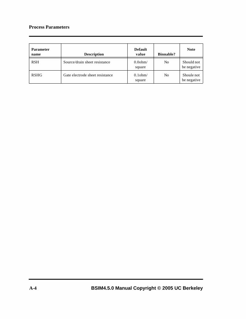
Process Parameters
A-4 BSIM4.5.0 Manual Copyright © 2005 UC Berkeley
RSH Source/drain sheet resistance 0.0ohm/square
No Should not be negative
RSHG Gate electrode sheet resistance 0.1ohm/square
No Shoule not be negative
Parameter name Description
Default value Binnable?
Note
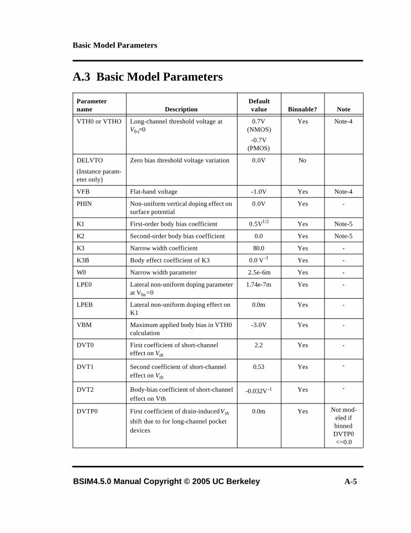
Basic Model Parameters
BSIM4.5.0 Manual Copyright © 2005 UC Berkeley A-5
A.3 Basic Model Parameters
Parameter name Description
Default value Binnable? Note
VTH0 or VTHO Long-channel threshold voltage at Vbs=0
0.7V (NMOS)
-0.7V (PMOS)
Yes Note-4
DELVTO
(Instance param-eter only)
Zero bias threshold voltage variation 0.0V No
VFB Flat-band voltage -1.0V Yes Note-4
PHIN Non-uniform vertical doping effect on surface potential
0.0V Yes -
K1 First-order body bias coefficient 0.5V1/2 Yes Note-5
K2 Second-order body bias coefficient 0.0 Yes Note-5
K3 Narrow width coefficient 80.0 Yes -
K3B Body effect coefficient of K3 0.0 V -1 Yes -
W0 Narrow width parameter 2.5e-6m Yes -
LPE0 Lateral non-uniform doping parameter at Vbs=0
1.74e-7m Yes -
LPEB Lateral non-uniform doping effect on K1
0.0m Yes -
VBM Maximum applied body bias in VTH0 calculation
-3.0V Yes -
DVT0 First coefficient of short-channel effect on Vth
2.2 Yes -
DVT1 Second coefficient of short-channel effect on Vth
0.53 Yes -
DVT2 Body-bias coefficient of short-channel effect on Vth
-0.032V -1 Yes -
DVTP0 First coefficient of drain-induced V th
shift due to for long-channel pocket devices
0.0m Yes Not mod-eled if binned DVTP0 <=0.0
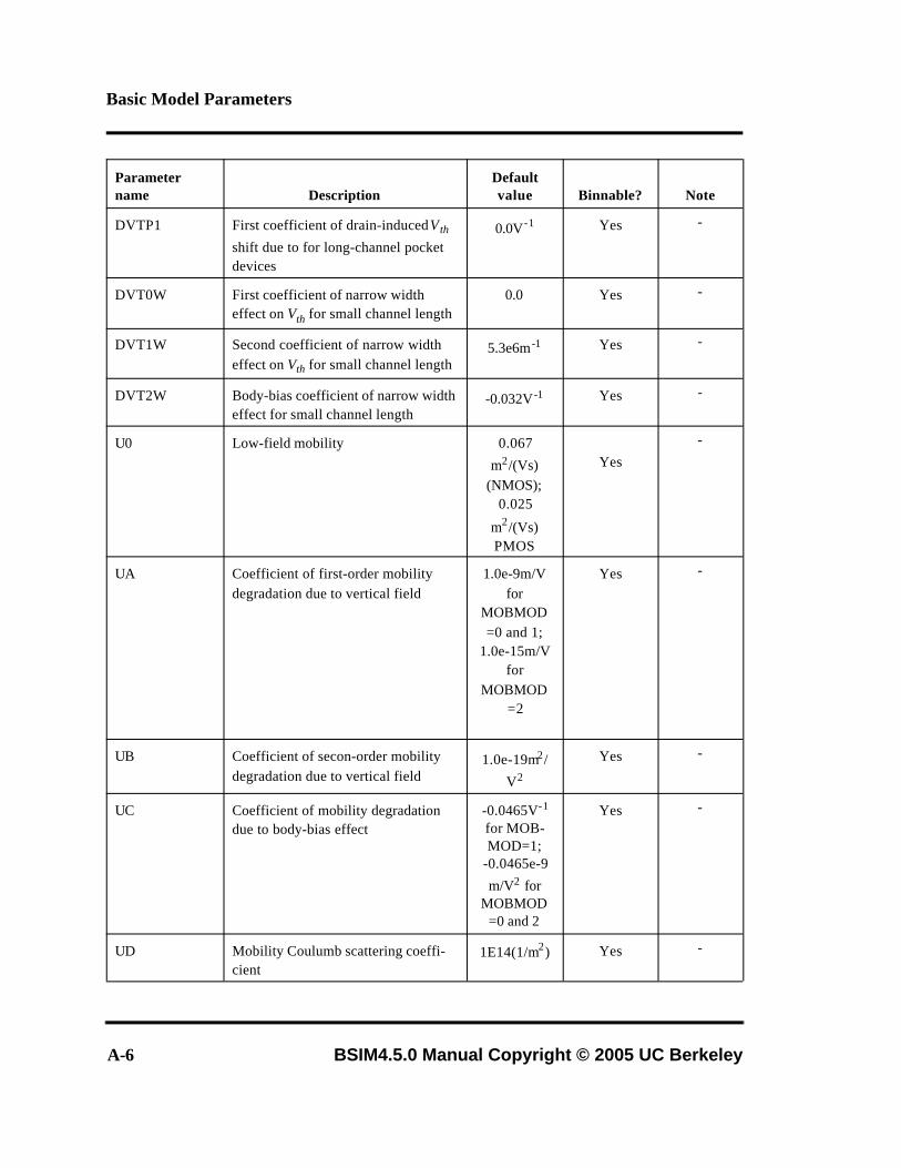
Basic Model Parameters
A-6 BSIM4.5.0 Manual Copyright © 2005 UC Berkeley
DVTP1 First coefficient of drain-induced V th
shift due to for long-channel pocket devices
0.0V-1 Yes -
DVT0W First coefficient of narrow width effect on Vth for small channel length
0.0 Yes -
DVT1W Second coefficient of narrow width effect on Vth for small channel length
5.3e6m -1 Yes -
DVT2W Body-bias coefficient of narrow width effect for small channel length
-0.032V -1 Yes -
U0 Low-field mobility 0.067
m2/(Vs) (NMOS);
0.025
m2/(Vs) PMOS
Yes
-
UA Coefficient of first-order mobility degradation due to vertical field
1.0e-9m/V for
MOBMOD=0 and 1;
1.0e-15m/V for
MOBMOD=2
Yes -
UB Coefficient of secon-order mobility degradation due to vertical field
1.0e-19m2/
V2
Yes -
UC Coefficient of mobility degradation due to body-bias effect
-0.0465V-1 for MOB-MOD=1;
-0.0465e-9
m/V2 for MOBMOD
=0 and 2
Yes -
UD Mobility Coulumb scattering coeffi-cient
1E14(1/m2) Yes -
Parameter name Description
Default value Binnable? Note
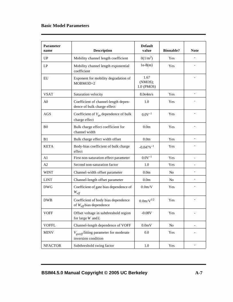
Basic Model Parameters
BSIM4.5.0 Manual Copyright © 2005 UC Berkeley A-7
UP Mobility channel length coefficient 0(1/m2) Yes -
LP Mobility channel length exponential coefficient
1e-8(m) Yes -
EU Exponent for mobility degradation of MOBMOD=2
1.67 (NMOS);
1.0 (PMOS)
-
VSAT Saturation velocity 8.0e4m/s Yes -
A0 Coefficient of channel-length depen-dence of bulk charge effect
1.0 Yes -
AGS Coefficient of Vgs dependence of bulk
charge effect0.0V-1 Yes -
B0 Bulk charge effect coefficient for channel width
0.0m Yes -
B1 Bulk charge effect width offset 0.0m Yes -
KETA Body-bias coefficient of bulk charge effect
-0.047V -1 Yes -
A1 First non-saturation effect parameter 0.0V-1 Yes -
A2 Second non-saturation factor 1.0 Yes -
WINT Channel-width offset parameter 0.0m No -
LINT Channel-length offset parameter 0.0m No -
DWG Coefficient of gate bias dependence of Weff
0.0m/V Yes -
DWB Coefficient of body bias dependence of Weff bias dependence
0.0m/V1/2 Yes -
VOFF Offset voltage in subthreshold region for large W and L
-0.08V Yes -
VOFFL Channel-length dependence of VOFF 0.0mV No -
MINV Vgsteff fitting parameter for moderate
inversion condition
0.0 Yes -
NFACTOR Subthreshold swing factor 1.0 Yes -
Parameter name Description
Default value Binnable? Note
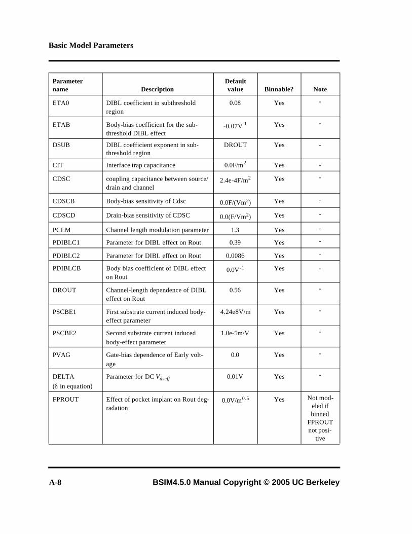
Basic Model Parameters
A-8 BSIM4.5.0 Manual Copyright © 2005 UC Berkeley
ETA0 DIBL coefficient in subthreshold region
0.08 Yes -
ETAB Body-bias coefficient for the sub-threshold DIBL effect
-0.07V-1 Yes -
DSUB DIBL coefficient exponent in sub-threshold region
DROUT Yes -
CIT Interface trap capacitance 0.0F/m2 Yes -
CDSC coupling capacitance between source/drain and channel
2.4e-4F/m2 Yes -
CDSCB Body-bias sensitivity of Cdsc 0.0F/(Vm2) Yes -
CDSCD Drain-bias sensitivity of CDSC 0.0(F/Vm2) Yes -
PCLM Channel length modulation parameter 1.3 Yes -
PDIBLC1 Parameter for DIBL effect on Rout 0.39 Yes -
PDIBLC2 Parameter for DIBL effect on Rout 0.0086 Yes -
PDIBLCB Body bias coefficient of DIBL effect on Rout
0.0V-1 Yes -
DROUT Channel-length dependence of DIBL effect on Rout
0.56 Yes -
PSCBE1 First substrate current induced body-effect parameter
4.24e8V/m Yes -
PSCBE2 Second substrate current induced body-effect parameter
1.0e-5m/V Yes -
PVAG Gate-bias dependence of Early volt-age
0.0 Yes -
DELTA(δ in equation)
Parameter for DC Vdseff 0.01V Yes -
FPROUT Effect of pocket implant on Rout deg-radation
0.0V/m0.5 Yes Not mod-eled if binned
FPROUT not posi-
tive
Parameter name Description
Default value Binnable? Note
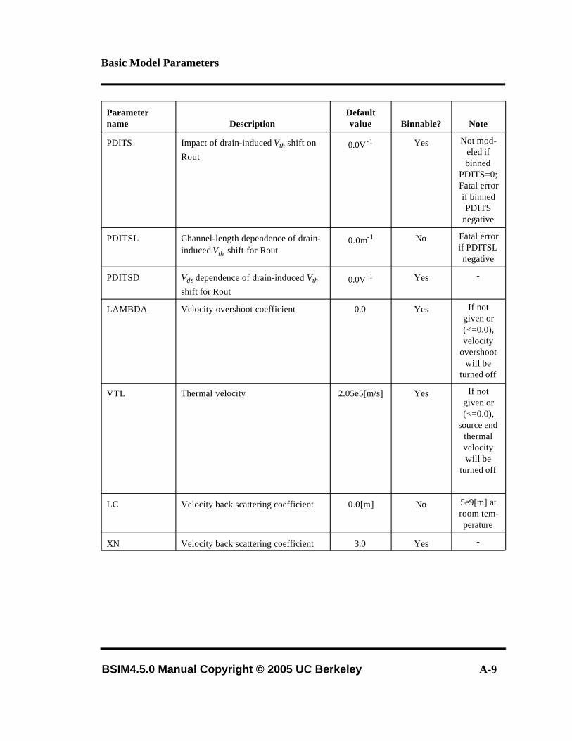
Basic Model Parameters
BSIM4.5.0 Manual Copyright © 2005 UC Berkeley A-9
PDITS Impact of drain-induced Vth shift on
Rout0.0V-1 Yes Not mod-
eled if binned
PDITS=0;Fatal error if binned PDITS
negative
PDITSL Channel-length dependence of drain-induced Vth shift for Rout
0.0m-1 No Fatal error if PDITSL negative
PDITSD Vds dependence of drain-induced Vth
shift for Rout0.0V-1 Yes -
LAMBDA Velocity overshoot coefficient 0.0 Yes If not given or (<=0.0), velocity
overshoot will be
turned off
VTL Thermal velocity 2.05e5[m/s] Yes If not given or (<=0.0),
source end thermal velocity will be
turned off
LC Velocity back scattering coefficient 0.0[m] No 5e9[m] at room tem-perature
XN Velocity back scattering coefficient 3.0 Yes -
Parameter name Description
Default value Binnable? Note
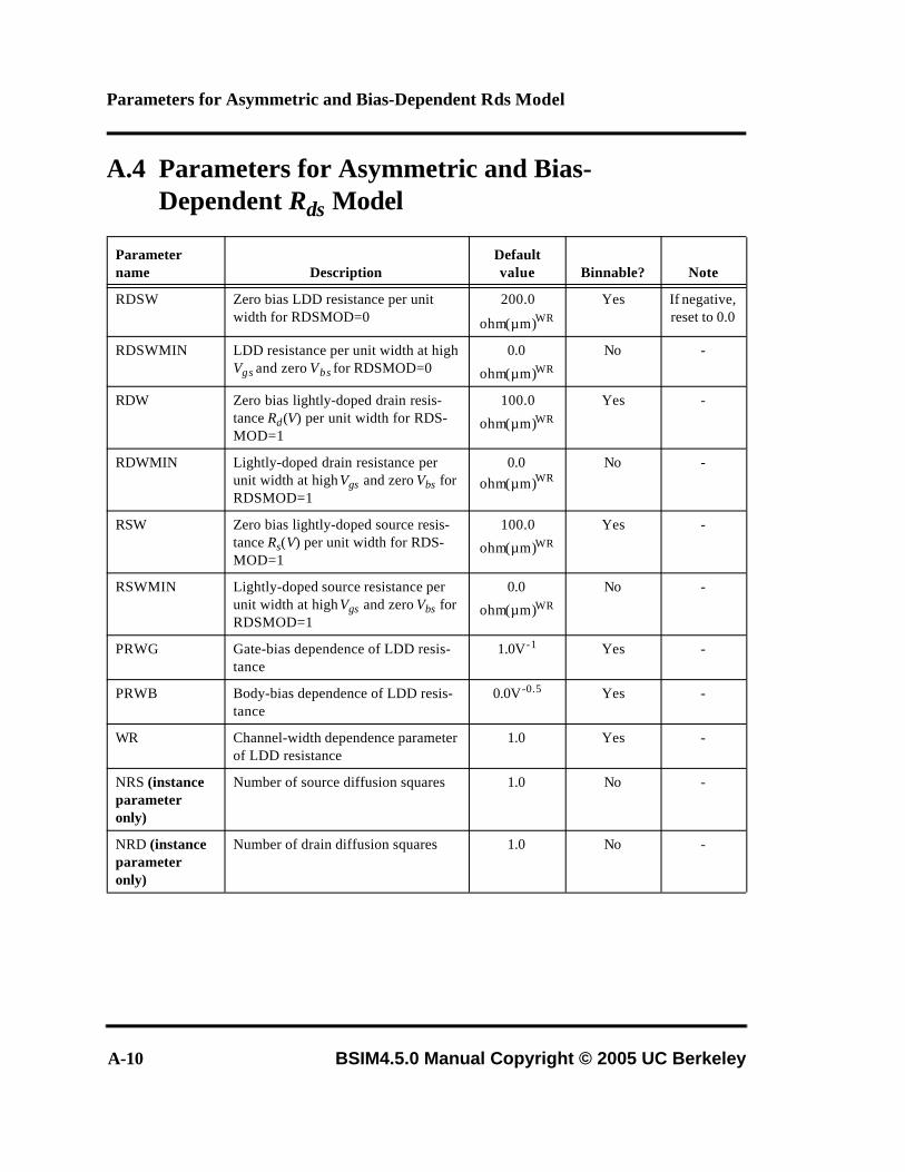
Parameters for Asymmetric and Bias-Dependent Rds Model
A-10 BSIM4.5.0 Manual Copyright © 2005 UC Berkeley
A.4 Parameters for Asymmetric and Bias-Dependent Rds Model
Parameter name Description
Default value Binnable? Note
RDSW Zero bias LDD resistance per unit width for RDSMOD=0
200.0
ohm(µm)WR
Yes If negative, reset to 0.0
RDSWMIN LDD resistance per unit width at high Vgs and zero Vbs for RDSMOD=0
0.0
ohm(µm)WR
No -
RDW Zero bias lightly-doped drain resis-tance Rd(V) per unit width for RDS-MOD=1
100.0
ohm(µm)WR
Yes -
RDWMIN Lightly-doped drain resistance per unit width at high Vgs and zero Vbs for RDSMOD=1
0.0ohm(µm)WR
No -
RSW Zero bias lightly-doped source resis-tance Rs(V) per unit width for RDS-MOD=1
100.0
ohm(µm)WR
Yes -
RSWMIN Lightly-doped source resistance per unit width at high Vgs and zero Vbs for RDSMOD=1
0.0
ohm(µm)WR
No -
PRWG Gate-bias dependence of LDD resis-tance
1.0V-1 Yes -
PRWB Body-bias dependence of LDD resis-tance
0.0V-0.5 Yes -
WR Channel-width dependence parameter of LDD resistance
1.0 Yes -
NRS (instance parameter only)
Number of source diffusion squares 1.0 No -
NRD (instance parameter only)
Number of drain diffusion squares 1.0 No -
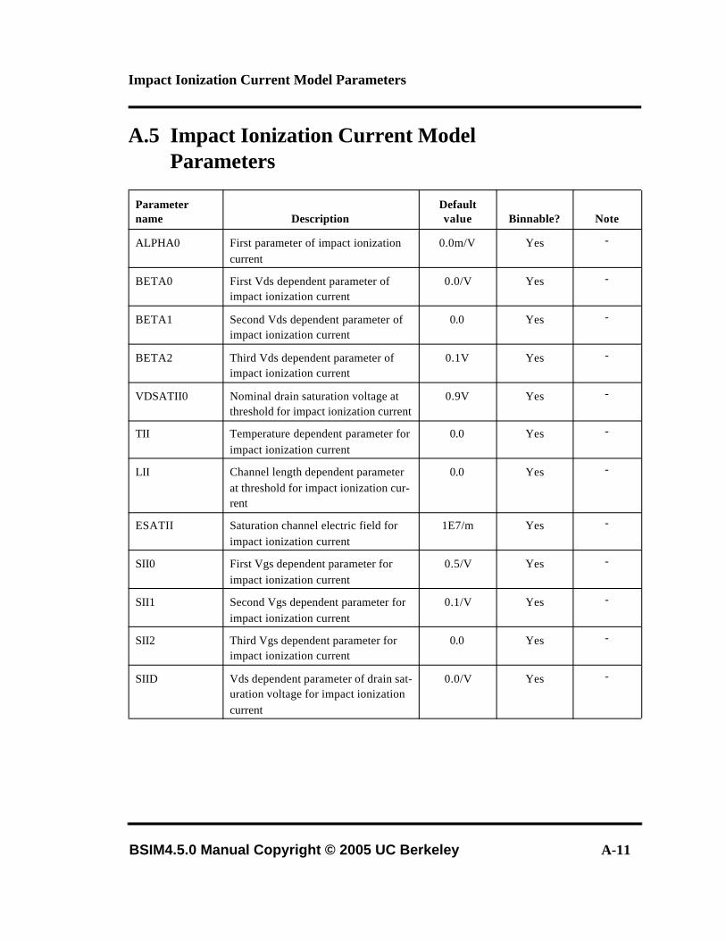
Impact Ionization Current Model Parameters
BSIM4.5.0 Manual Copyright © 2005 UC Berkeley A-11
A.5 Impact Ionization Current Model Parameters
Parameter name Description
Default value Binnable? Note
ALPHA0 First parameter of impact ionization current
0.0m/V Yes -
BETA0 First Vds dependent parameter of impact ionization current
0.0/V Yes -
BETA1 Second Vds dependent parameter of impact ionization current
0.0 Yes -
BETA2 Third Vds dependent parameter of impact ionization current
0.1V Yes -
VDSATII0 Nominal drain saturation voltage at threshold for impact ionization current
0.9V Yes -
TII Temperature dependent parameter for impact ionization current
0.0 Yes -
LII Channel length dependent parameter at threshold for impact ionization cur-rent
0.0 Yes -
ESATII Saturation channel electric field for impact ionization current
1E7/m Yes -
SII0 First Vgs dependent parameter for impact ionization current
0.5/V Yes -
SII1 Second Vgs dependent parameter for impact ionization current
0.1/V Yes -
SII2 Third Vgs dependent parameter for impact ionization current
0.0 Yes -
SIID Vds dependent parameter of drain sat-uration voltage for impact ionization current
0.0/V Yes -
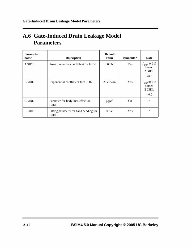
Gate-Induced Drain Leakage Model Parameters
A-12 BSIM4.5.0 Manual Copyright © 2005 UC Berkeley
A.6 Gate-Induced Drain Leakage Model Parameters
Parameter name Description
Default value Binnable? Note
AGIDL Pre-exponential coefficient for GIDL 0.0mho Yes Igidl=0.0 if binned AGIDL
=0.0
BGIDL Exponential coefficient for GIDL 2.3e9V/m Yes Igidl=0.0 if binned BGIDL
=0.0
CGIDL Paramter for body-bias effect on GIDL
0.5V3 Yes -
EGIDL Fitting parameter for band bending for GIDL
0.8V Yes -
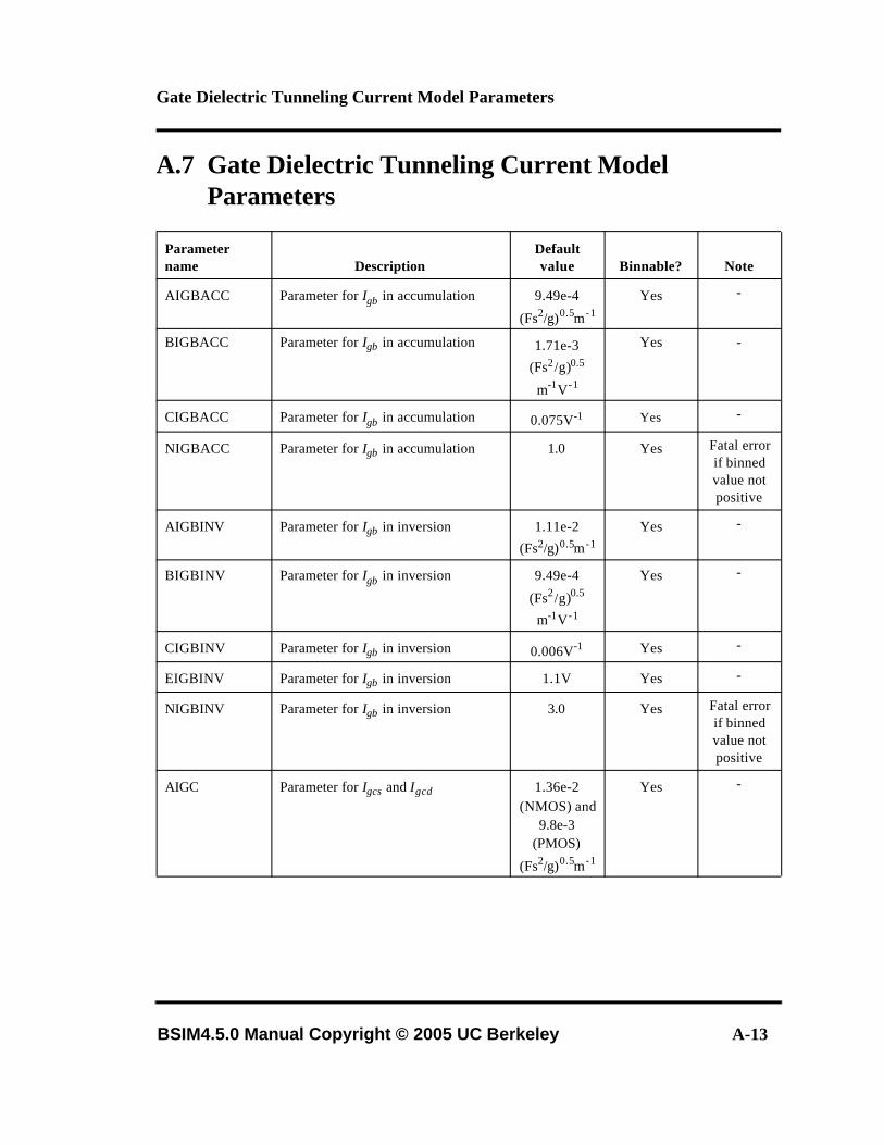
Gate Dielectric Tunneling Current Model Parameters
BSIM4.5.0 Manual Copyright © 2005 UC Berkeley A-13
A.7 Gate Dielectric Tunneling Current Model Parameters
Parameter name Description
Default value Binnable? Note
AIGBACC Parameter for Igb in accumulation 9.49e-4
(Fs2/g)0.5m-1Yes -
BIGBACC Parameter for Igb in accumulation 1.71e-3
(Fs2/g)0.5
m-1V-1
Yes -
CIGBACC Parameter for Igb in accumulation 0.075V-1 Yes -
NIGBACC Parameter for Igb in accumulation 1.0 Yes Fatal error if binned value not positive
AIGBINV Parameter for Igb in inversion 1.11e-2
(Fs2/g)0.5m-1Yes -
BIGBINV Parameter for Igb in inversion 9.49e-4
(Fs2/g)0.5
m-1V-1
Yes -
CIGBINV Parameter for Igb in inversion 0.006V-1 Yes -
EIGBINV Parameter for Igb in inversion 1.1V Yes -
NIGBINV Parameter for Igb in inversion 3.0 Yes Fatal error if binned value not positive
AIGC Parameter for Igcs and Igcd 1.36e-2 (NMOS) and
9.8e-3 (PMOS)
(Fs2/g)0.5m-1
Yes -
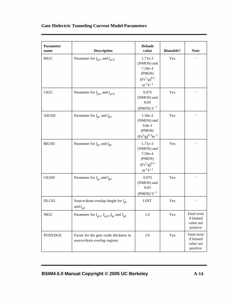
Gate Dielectric Tunneling Current Model Parameters
BSIM4.5.0 Manual Copyright © 2005 UC Berkeley A-14
BIGC Parameter for Igcs and Igcd 1.71e-3 (NMOS) and
7.59e-4 (PMOS)
(Fs2/g)0.5
m-1V-1
Yes -
CIGC Parameter for Igcs and Igcd 0.075 (NMOS) and
0.03
(PMOS) V -1
Yes -
AIGSD Parameter for Igs and Igd 1.36e-2 (NMOS) and
9.8e-3 (PMOS)
(Fs2/g)0.5m-1
Yes -
BIGSD Parameter for Igs and Igd 1.71e-3 (NMOS) and
7.59e-4 (PMOS)
(Fs2/g)0.5
m-1V-1
Yes -
CIGSD Parameter for Igs and Igd 0.075 (NMOS) and
0.03
(PMOS) V -1
Yes -
DLCIG Source/drain overlap length for Igs
and Igd
LINT Yes -
NIGC Parameter for Igcs, Igcd ,Igs and Igd 1.0 Yes Fatal error if binned value not positive
POXEDGE Factor for the gate oxide thickness in source/drain overlap regions
1.0 Yes Fatal error if binned value not positive
Parameter name Description
Default value Binnable? Note
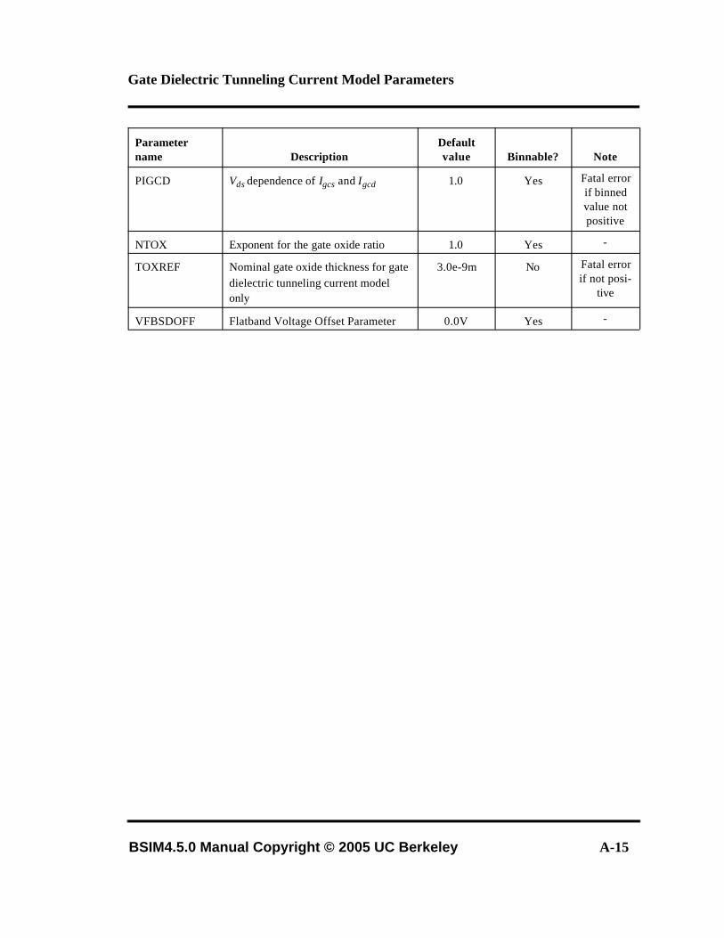
Gate Dielectric Tunneling Current Model Parameters
BSIM4.5.0 Manual Copyright © 2005 UC Berkeley A-15
PIGCD Vds dependence of Igcs and Igcd 1.0 Yes Fatal error if binned value not positive
NTOX Exponent for the gate oxide ratio 1.0 Yes -
TOXREF Nominal gate oxide thickness for gate dielectric tunneling current model only
3.0e-9m No Fatal error if not posi-
tive
VFBSDOFF Flatband Voltage Offset Parameter 0.0V Yes -
Parameter name Description
Default value Binnable? Note
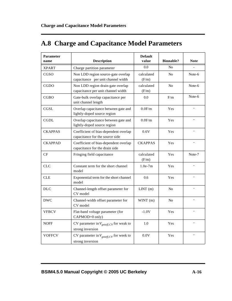
Charge and Capacitance Model Parameters
BSIM4.5.0 Manual Copyright © 2005 UC Berkeley A-16
A.8 Charge and Capacitance Model Parameters
Parameter name Description
Default value Binnable? Note
XPART Charge partition parameter 0.0 No -
CGSO Non LDD region source-gate overlap capacitance per unit channel width
calculated (F/m)
No Note-6
CGDO Non LDD region drain-gate overlap capacitance per unit channel width
calculated(F/m)
No Note-6
CGBO Gate-bulk overlap capacitance per unit channel length
0.0 F/m Note-6
CGSL Overlap capacitance between gate and lightly-doped source region
0.0F/m Yes -
CGDL Overlap capacitance between gate and lightly-doped source region
0.0F/m Yes -
CKAPPAS Coefficient of bias-dependent overlap capacitance for the source side
0.6V Yes -
CKAPPAD Coefficient of bias-dependent overlap capacitance for the drain side
CKAPPAS Yes -
CF Fringing field capacitance calculated(F/m)
Yes Note-7
CLC Constant term for the short channel model
1.0e-7m Yes -
CLE Exponential term for the short channel model
0.6 Yes -
DLC Channel-length offset parameter for CV model
LINT (m) No -
DWC Channel-width offset parameter for CV model
WINT (m) No -
VFBCV Flat-band voltage parameter (for CAPMOD=0 only)
-1.0V Yes -
NOFF CV parameter in Vgsteff,CV for weak to
strong inversion
1.0 Yes -
VOFFCV CV parameter in Vgsteff,CV for week to
strong inversion
0.0V Yes -
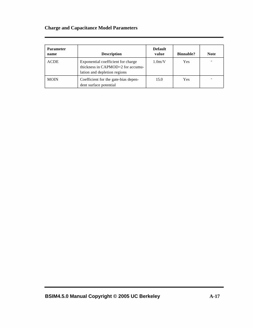
Charge and Capacitance Model Parameters
BSIM4.5.0 Manual Copyright © 2005 UC Berkeley A-17
ACDE Exponential coefficient for charge thickness in CAPMOD=2 for accumu-lation and depletion regions
1.0m/V Yes -
MOIN Coefficient for the gate-bias depen-dent surface potential
15.0 Yes -
Parameter name Description
Default value Binnable? Note
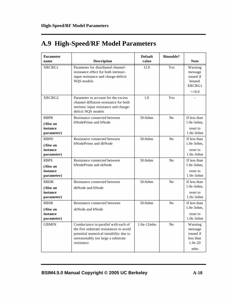
High-Speed/RF Model Parameters
BSIM4.5.0 Manual Copyright © 2005 UC Berkeley A-18
A.9 High-Speed/RF Model Parameters
Parameter name Description
Default value
Binnable?Note
XRCRG1 Parameter for distributed channel-resistance effect for both intrinsic-input resistance and charge-deficit NQS models
12.0 Yes Warning message issued if binned
XRCRG1
<=0.0
XRCRG2 Parameter to account for the excess channel diffusion resistance for both intrinsic input resistance and charge-deficit NQS models
1.0 Yes -
RBPB
(Also an instance parameter)
Resistance connected between bNodePrime and bNode
50.0ohm No If less than 1.0e-3ohm,
reset to 1.0e-3ohm
RBPD
(Also an instance parameter)
Resistance connected between bNodePrime and dbNode
50.0ohm No If less than 1.0e-3ohm,
reset to 1.0e-3ohm
RBPS
(Also an instance parameter)
Resistance connected between bNodePrime and sbNode
50.0ohm No If less than 1.0e-3ohm,
reset to 1.0e-3ohm
RBDB
(Also an instance parameter)
Resistance connected between
dbNode and bNode
50.0ohm No If less than 1.0e-3ohm,
reset to 1.0e-3ohm
RBSB
(Also an instance parameter)
Resistance connected between
sbNode and bNode
50.0ohm No If less than 1.0e-3ohm,
reset to 1.0e-3ohm
GBMIN Conductance in parallel with each of the five substrate resistances to avoid potential numerical instability due to unreasonably too large a substrate resistance
1.0e-12mho No Warning message issued if less than 1.0e-20
mho

High-Speed/RF Model Parameters
BSIM4.5.0 Manual Copyright © 2005 UC Berkeley A-19
RBPS0 Scaling prefactor for RBPS 50 Ohms No
RBPSL Length Scaling parameter for RBPS 0.0 No
RBPSW Width Scaling parameter for RBPS 0.0 No
RBPSNF Number of fingers Scaling parameter for RBPS
0.0 No
RBPD0 Scaling prefactor for RBPD 50 Ohms No
RBPDL Length Scaling parameter for RBPD 0.0 No
RBPDW Width Scaling parameter for RBPD 0.0 No
RBPDNF Number of fingers Scaling parameter for RBPD
0.0 No
RBPBX0 Scaling prefactor for RBPBX 100 Ohms No
RBPBXL Length Scaling parameter forRBPBX 0.0 No
RBPBXW Width Scaling parameter for RBPBX 0.0 No
RBPBXNF Number of fingers Scaling parameter for RBPBX
0.0 No
RBPBY0 Scaling prefactor for RBPBY 100 Ohms No
RBPBYL Length Scaling parameter forRBPBY 0.0 No
RBPBYW Width Scaling parameter for RBPBY 0.0 No
RBPBYNF Number of fingers Scaling parameter for RBPBY
0.0 No
RBSBX0 Scaling prefactor for RBSBX 100 Ohms No
RBSBY0 Scaling prefactor for RBSBY 100 Ohms No
RBDBX0 Scaling prefactor for RBDBX 100 Ohms No
RBDBY0 Scaling prefactor for RBDBY 100 Ohms No
RBSDBXL Length Scaling parameter for RBSBX and RBDBX
0.0 No
RBSDBXW Width Scaling parameter for RBSBX and RBDBX
0.0 No
RBSDBXNF Number of fingers Scaling parameter for RBSBX and RBDBX
0.0 No
RBSDBYL Length Scaling parameter for RBSBY and RBDBY
0.0 No
RBSDBYW Width Scaling parameter for RBSBY and RBDBY
0.0 No
RBSDBYNF Number of fingers Scaling parameter for RBSBY and RBDBY
0.0 No
Parameter name Description
Default value
Binnable?Note
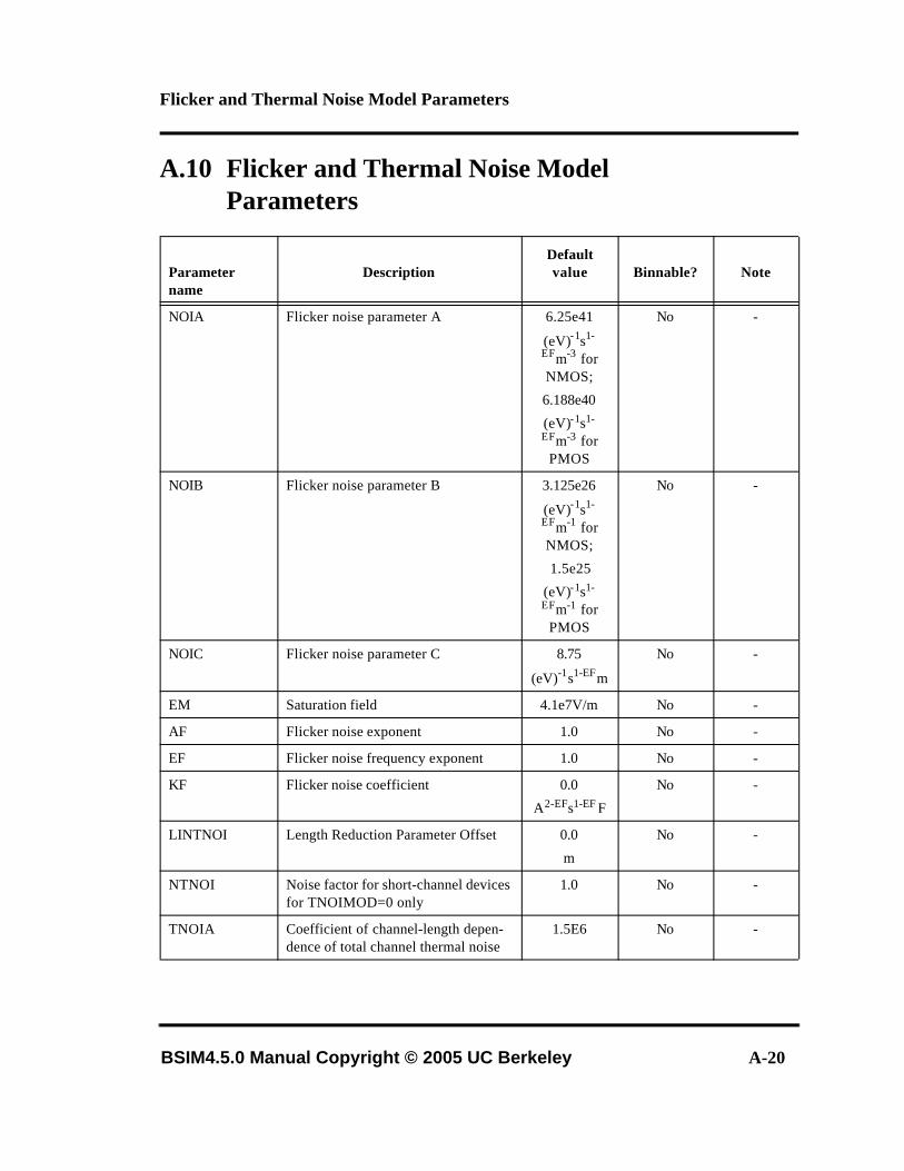
Flicker and Thermal Noise Model Parameters
BSIM4.5.0 Manual Copyright © 2005 UC Berkeley A-20
A.10 Flicker and Thermal Noise Model Parameters
Parameter name
DescriptionDefault value Binnable? Note
NOIA Flicker noise parameter A 6.25e41
(eV)-1s1-
EFm-3 for NMOS;
6.188e40
(eV)-1s1-
EFm-3 for PMOS
No -
NOIB Flicker noise parameter B 3.125e26
(eV)-1s1-
EFm-1 for NMOS;
1.5e25
(eV)-1s1-
EFm-1 for PMOS
No -
NOIC Flicker noise parameter C 8.75
(eV)-1s1-EFm
No -
EM Saturation field 4.1e7V/m No -
AF Flicker noise exponent 1.0 No -
EF Flicker noise frequency exponent 1.0 No -
KF Flicker noise coefficient 0.0
A2-EFs1-EF F
No -
LINTNOI Length Reduction Parameter Offset 0.0
m
No -
NTNOI Noise factor for short-channel devices for TNOIMOD=0 only
1.0 No -
TNOIA Coefficient of channel-length depen-dence of total channel thermal noise
1.5E6 No -
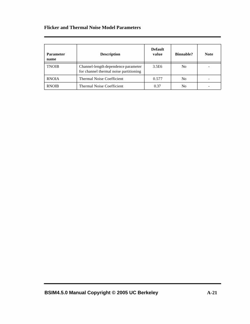
Flicker and Thermal Noise Model Parameters
BSIM4.5.0 Manual Copyright © 2005 UC Berkeley A-21
TNOIB Channel-length dependence parameter for channel thermal noise partitioning
3.5E6 No -
RNOIA Thermal Noise Coefficient 0.577 No -
RNOIB Thermal Noise Coefficient 0.37 No -
Parameter name
DescriptionDefault value Binnable? Note
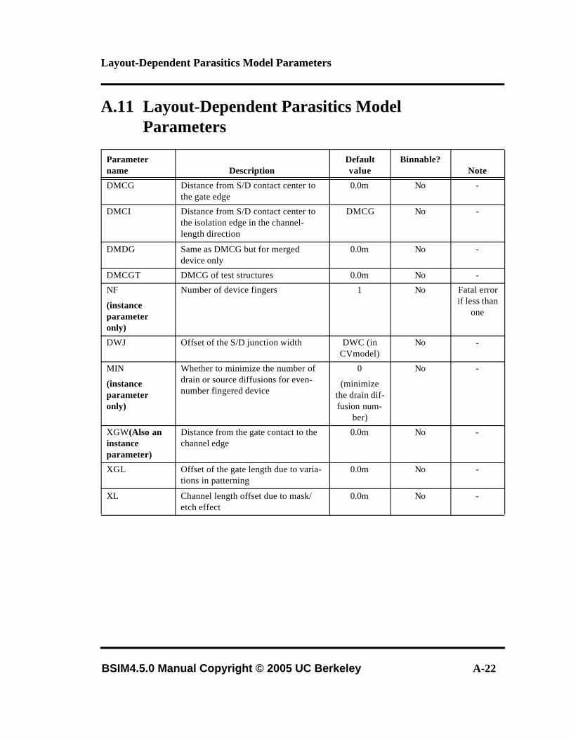
Layout-Dependent Parasitics Model Parameters
BSIM4.5.0 Manual Copyright © 2005 UC Berkeley A-22
A.11 Layout-Dependent Parasitics Model Parameters
Parameter name Description
Default value
Binnable?Note
DMCG Distance from S/D contact center to the gate edge
0.0m No -
DMCI Distance from S/D contact center to the isolation edge in the channel-length direction
DMCG No -
DMDG Same as DMCG but for merged device only
0.0m No -
DMCGT DMCG of test structures 0.0m No -
NF
(instance parameter only)
Number of device fingers 1 No Fatal error if less than
one
DWJ Offset of the S/D junction width DWC (in CVmodel)
No -
MIN
(instance parameter only)
Whether to minimize the number of drain or source diffusions for even-number fingered device
0
(minimize the drain dif-fusion num-
ber)
No -
XGW(Also an instance parameter)
Distance from the gate contact to the channel edge
0.0m No -
XGL Offset of the gate length due to varia-tions in patterning
0.0m No -
XL Channel length offset due to mask/etch effect
0.0m No -
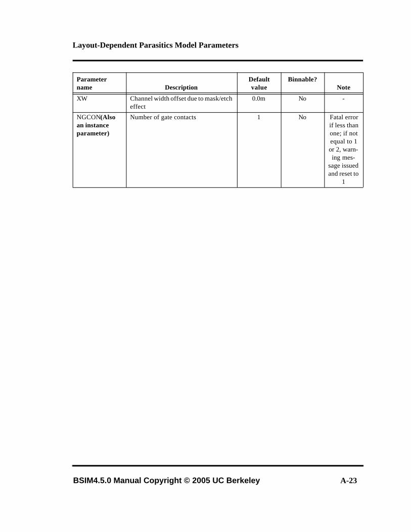
Layout-Dependent Parasitics Model Parameters
BSIM4.5.0 Manual Copyright © 2005 UC Berkeley A-23
XW Channel width offset due to mask/etch effect
0.0m No -
NGCON(Also an instance parameter)
Number of gate contacts 1 No Fatal error if less than one; if not equal to 1 or 2, warn-ing mes-
sage issued and reset to
1
Parameter name Description
Default value
Binnable?Note
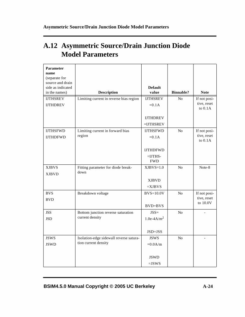
Asymmetric Source/Drain Junction Diode Model Parameters
BSIM4.5.0 Manual Copyright © 2005 UC Berkeley A-24
A.12 Asymmetric Source/Drain Junction Diode Model Parameters
Parameter name(separate for source and drain side as indicated in the names) Description
Default value Binnable? Note
IJTHSREV
IJTHDREV
Limiting current in reverse bias region IJTHSREV
=0.1A
IJTHDREV
=IJTHSREV
No If not posi-tive, reset to 0.1A
IJTHSFWD
IJTHDFWD
Limiting current in forward bias region
IJTHSFWD
=0.1A
IJTHDFWD
=IJTHS-FWD
No If not posi-tive, reset to 0.1A
XJBVS
XJBVD
Fitting parameter for diode break-down
XJBVS=1.0
XJBVD
=XJBVS
No Note-8
BVS
BVD
Breakdown voltage BVS=10.0V
BVD=BVS
No If not posi-tive, reset to 10.0V
JSS
JSD
Bottom junction reverse saturation current density
JSS=
1.0e-4A/m2
JSD=JSS
No -
JSWS
JSWD
Isolation-edge sidewall reverse satura-tion current density
JSWS
=0.0A/m
JSWD
=JSWS
No -
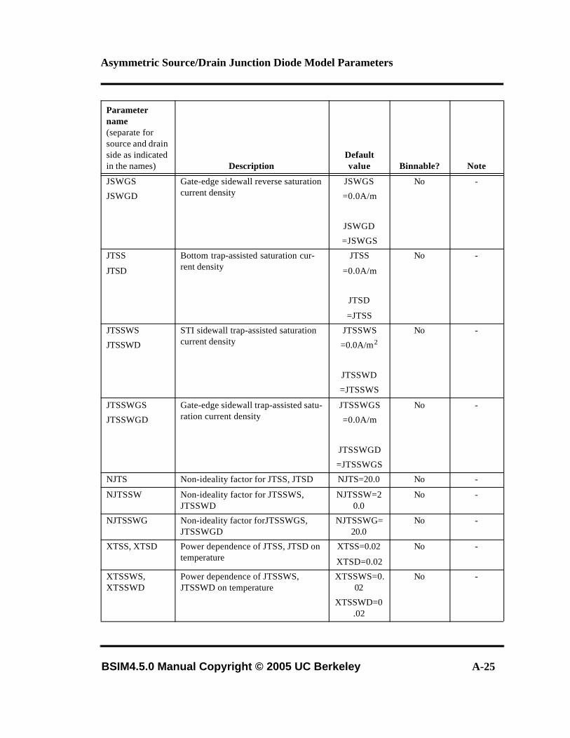
Asymmetric Source/Drain Junction Diode Model Parameters
BSIM4.5.0 Manual Copyright © 2005 UC Berkeley A-25
JSWGS
JSWGD
Gate-edge sidewall reverse saturation current density
JSWGS
=0.0A/m
JSWGD
=JSWGS
No -
JTSS
JTSD
Bottom trap-assisted saturation cur-rent density
JTSS
=0.0A/m
JTSD
=JTSS
No -
JTSSWS
JTSSWD
STI sidewall trap-assisted saturation current density
JTSSWS
=0.0A/m2
JTSSWD
=JTSSWS
No -
JTSSWGS
JTSSWGD
Gate-edge sidewall trap-assisted satu-ration current density
JTSSWGS
=0.0A/m
JTSSWGD
=JTSSWGS
No -
NJTS Non-ideality factor for JTSS, JTSD NJTS=20.0 No -
NJTSSW Non-ideality factor for JTSSWS, JTSSWD
NJTSSW=20.0
No -
NJTSSWG Non-ideality factor forJTSSWGS, JTSSWGD
NJTSSWG=20.0
No -
XTSS, XTSD Power dependence of JTSS, JTSD on temperature
XTSS=0.02
XTSD=0.02
No -
XTSSWS, XTSSWD
Power dependence of JTSSWS, JTSSWD on temperature
XTSSWS=0.02
XTSSWD=0.02
No -
Parameter name(separate for source and drain side as indicated in the names) Description
Default value Binnable? Note
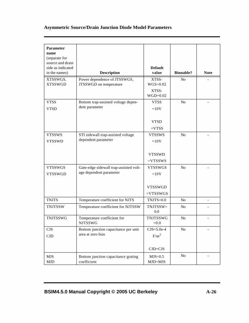
Asymmetric Source/Drain Junction Diode Model Parameters
BSIM4.5.0 Manual Copyright © 2005 UC Berkeley A-26
XTSSWGS, XTSSWGD
Power dependence of JTSSWGS, JTSSWGD on temperature
XTSS-WGS=0.02
XTSS-WGD=0.02
No -
VTSS
VTSD
Bottom trap-assisted voltage depen-dent parameter
VTSS
=10V
VTSD
=VTSS
No -
VTSSWS
VTSSWD
STI sidewall trap-assisted voltage dependent parameter
VTSSWS
=10V
VTSSWD
=VTSSWS
No -
VTSSWGS
VTSSWGD
Gate-edge sidewall trap-assisted volt-age dependent parameter
VTSSWGS
=10V
VTSSWGD
=VTSSWGS
No -
TNJTS Temperature coefficient for NJTS TNJTS=0.0 No -
TNJTSSW Temperature coefficient for NJTSSW TNJTSSW=0.0
No -
TNJTSSWG Temperature coefficient for NJTSSWG
TNJTSSWG=0.0
No -
CJS
CJD
Bottom junction capacitance per unit area at zero bias
CJS=5.0e-4
F/m2
CJD=CJS
No -
MJSMJD
Bottom junction capacitance grating coefficient
MJS=0.5MJD=MJS
No -
Parameter name(separate for source and drain side as indicated in the names) Description
Default value Binnable? Note
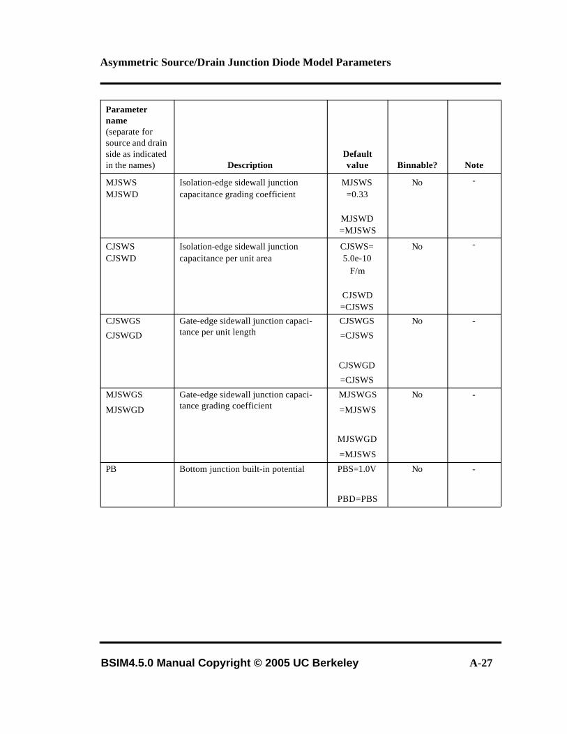
Asymmetric Source/Drain Junction Diode Model Parameters
BSIM4.5.0 Manual Copyright © 2005 UC Berkeley A-27
MJSWSMJSWD
Isolation-edge sidewall junction capacitance grading coefficient
MJSWS=0.33
MJSWD=MJSWS
No -
CJSWSCJSWD
Isolation-edge sidewall junction capacitance per unit area
CJSWS=5.0e-10
F/m
CJSWD=CJSWS
No -
CJSWGS
CJSWGD
Gate-edge sidewall junction capaci-tance per unit length
CJSWGS
=CJSWS
CJSWGD
=CJSWS
No -
MJSWGS
MJSWGD
Gate-edge sidewall junction capaci-tance grading coefficient
MJSWGS
=MJSWS
MJSWGD
=MJSWS
No -
PB Bottom junction built-in potential PBS=1.0V
PBD=PBS
No -
Parameter name(separate for source and drain side as indicated in the names) Description
Default value Binnable? Note
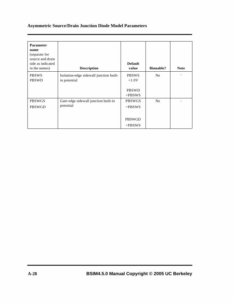
Asymmetric Source/Drain Junction Diode Model Parameters
A-28 BSIM4.5.0 Manual Copyright © 2005 UC Berkeley
PBSWSPBSWD
Isolation-edge sidewall junction built-in potential
PBSWS=1.0V
PBSWD=PBSWS
No -
PBSWGS
PBSWGD
Gate-edge sidewall junction built-in potential
PBSWGS
=PBSWS
PBSWGD
=PBSWS
No -
Parameter name(separate for source and drain side as indicated in the names) Description
Default value Binnable? Note
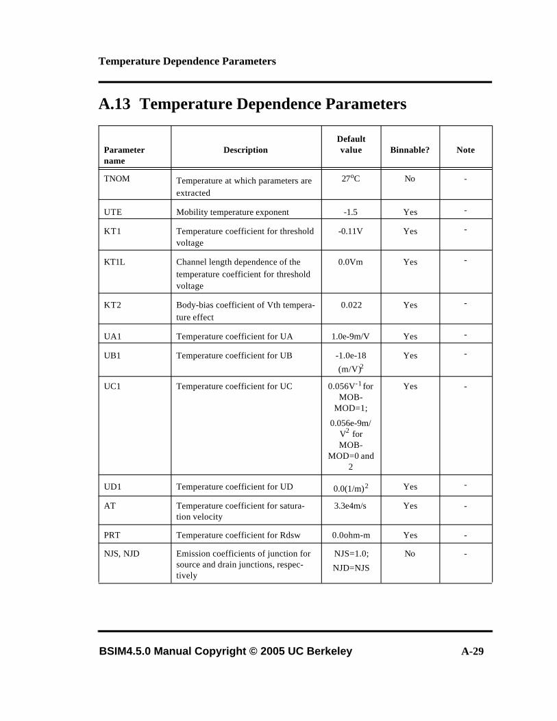
Temperature Dependence Parameters
BSIM4.5.0 Manual Copyright © 2005 UC Berkeley A-29
A.13 Temperature Dependence Parameters
Parameter name
DescriptionDefault value Binnable? Note
TNOM Temperature at which parameters are extracted
27oC No -
UTE Mobility temperature exponent -1.5 Yes -
KT1 Temperature coefficient for threshold voltage
-0.11V Yes -
KT1L Channel length dependence of the temperature coefficient for threshold voltage
0.0Vm Yes -
KT2 Body-bias coefficient of Vth tempera-ture effect
0.022 Yes -
UA1 Temperature coefficient for UA 1.0e-9m/V Yes -
UB1 Temperature coefficient for UB -1.0e-18
(m/V)2Yes -
UC1 Temperature coefficient for UC 0.056V-1 for MOB-
MOD=1;
0.056e-9m/V2 for MOB-
MOD=0 and 2
Yes -
UD1 Temperature coefficient for UD 0.0(1/m)2 Yes -
AT Temperature coefficient for satura-tion velocity
3.3e4m/s Yes -
PRT Temperature coefficient for Rdsw 0.0ohm-m Yes -
NJS, NJD Emission coefficients of junction for source and drain junctions, respec-tively
NJS=1.0;
NJD=NJS
No -
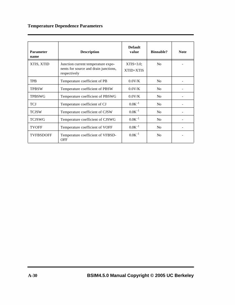
Temperature Dependence Parameters
A-30 BSIM4.5.0 Manual Copyright © 2005 UC Berkeley
XTIS, XTID Junction current temperature expo-nents for source and drain junctions, respectively
XTIS=3.0;
XTID=XTIS
No -
TPB Temperature coefficient of PB 0.0V/K No -
TPBSW Temperature coefficient of PBSW 0.0V/K No -
TPBSWG Temperature coefficient of PBSWG 0.0V/K No -
TCJ Temperature coefficient of CJ 0.0K-1 No -
TCJSW Temperature coefficient of CJSW 0.0K-1 No -
TCJSWG Temperature coefficient of CJSWG 0.0K-1 No -
TVOFF Temperature coefficient of VOFF 0.0K-1 No -
TVFBSDOFF Temperature coefficient of VFBSD-OFF
0.0K-1 No -
Parameter name
DescriptionDefault value Binnable? Note
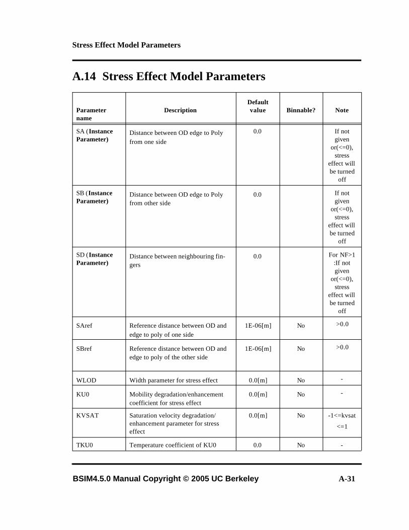
Stress Effect Model Parameters
BSIM4.5.0 Manual Copyright © 2005 UC Berkeley A-31
A.14 Stress Effect Model Parameters
Parameter name
DescriptionDefault value Binnable? Note
SA (Instance Parameter)
Distance between OD edge to Poly from one side
0.0 If not given
or(<=0), stress
effect will be turned
off
SB (Instance Parameter)
Distance between OD edge to Poly from other side
0.0 If not given
or(<=0), stress
effect will be turned
off
SD (Instance Parameter)
Distance between neighbouring fin-gers
0.0 For NF>1 :If not given
or(<=0), stress
effect will be turned
off
SAref Reference distance between OD and edge to poly of one side
1E-06[m] No >0.0
SBref Reference distance between OD and edge to poly of the other side
1E-06[m] No >0.0
WLOD Width parameter for stress effect 0.0[m] No -
KU0 Mobility degradation/enhancement coefficient for stress effect
0.0[m] No -
KVSAT Saturation velocity degradation/enhancement parameter for stress effect
0.0[m] No -1<=kvsat
<=1
TKU0 Temperature coefficient of KU0 0.0 No -
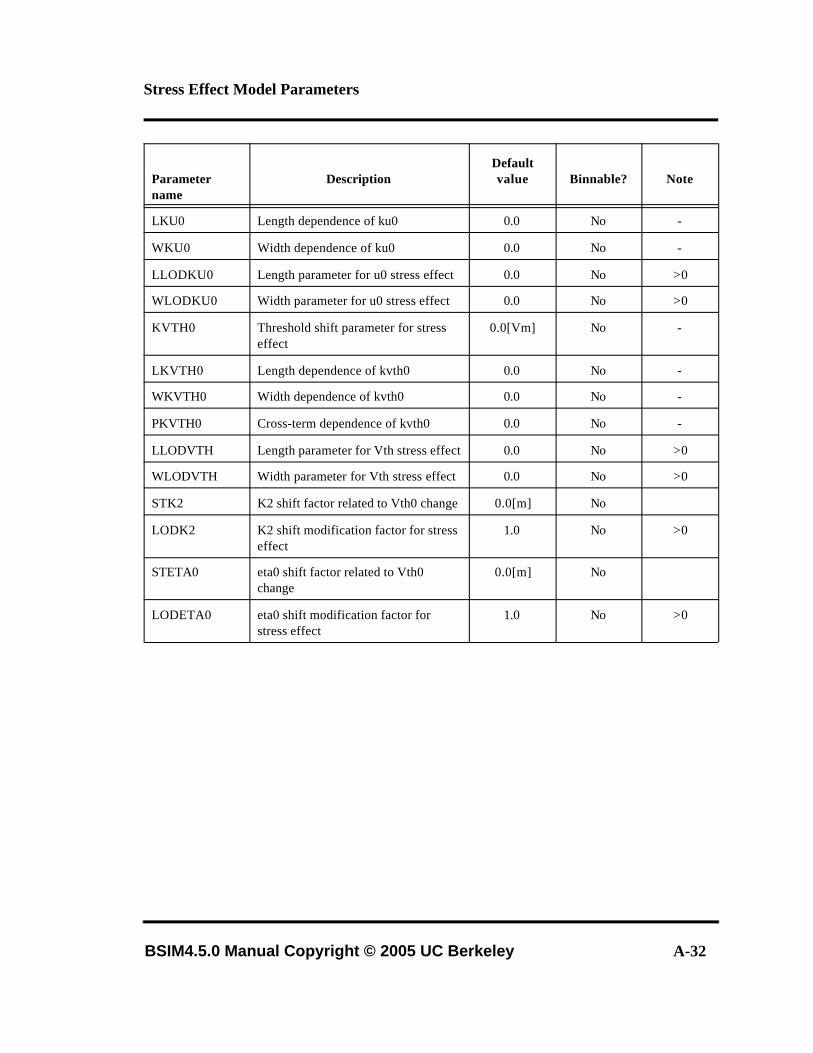
Stress Effect Model Parameters
BSIM4.5.0 Manual Copyright © 2005 UC Berkeley A-32
LKU0 Length dependence of ku0 0.0 No -
WKU0 Width dependence of ku0 0.0 No -
LLODKU0 Length parameter for u0 stress effect 0.0 No >0
WLODKU0 Width parameter for u0 stress effect 0.0 No >0
KVTH0 Threshold shift parameter for stress effect
0.0[Vm] No -
LKVTH0 Length dependence of kvth0 0.0 No -
WKVTH0 Width dependence of kvth0 0.0 No -
PKVTH0 Cross-term dependence of kvth0 0.0 No -
LLODVTH Length parameter for Vth stress effect 0.0 No >0
WLODVTH Width parameter for Vth stress effect 0.0 No >0
STK2 K2 shift factor related to Vth0 change 0.0[m] No
LODK2 K2 shift modification factor for stress effect
1.0 No >0
STETA0 eta0 shift factor related to Vth0 change
0.0[m] No
LODETA0 eta0 shift modification factor for stress effect
1.0 No >0
Parameter name
DescriptionDefault value Binnable? Note
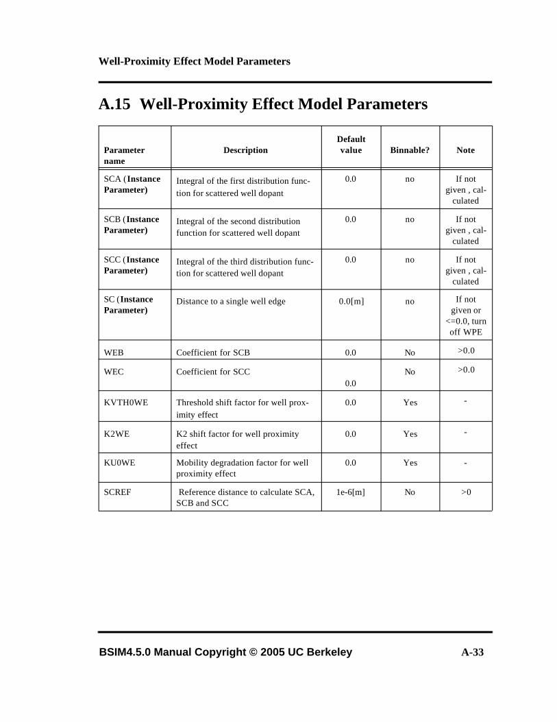
Well-Proximity Effect Model Parameters
BSIM4.5.0 Manual Copyright © 2005 UC Berkeley A-33
A.15 Well-Proximity Effect Model Parameters
Parameter name
DescriptionDefault value Binnable? Note
SCA (Instance Parameter)
Integral of the first distribution func-tion for scattered well dopant
0.0 no If not given , cal-
culated
SCB (Instance Parameter)
Integral of the second distribution function for scattered well dopant
0.0 no If not given , cal-
culated
SCC (Instance Parameter)
Integral of the third distribution func-tion for scattered well dopant
0.0 no If not given , cal-
culated
SC (Instance Parameter)
Distance to a single well edge 0.0[m] no If not given or
<=0.0, turn off WPE
WEB Coefficient for SCB 0.0 No >0.0
WEC Coefficient for SCC0.0
No >0.0
KVTH0WE Threshold shift factor for well prox-imity effect
0.0 Yes -
K2WE K2 shift factor for well proximity effect
0.0 Yes -
KU0WE Mobility degradation factor for well proximity effect
0.0 Yes -
SCREF Reference distance to calculate SCA, SCB and SCC
1e-6[m] No >0
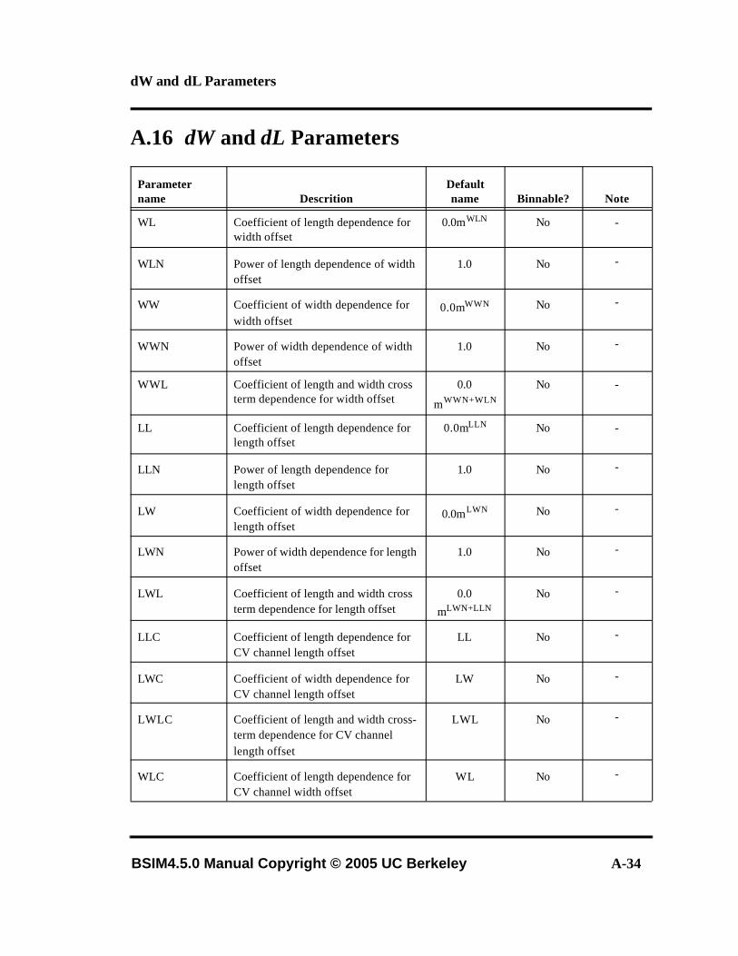
dW and dL Parameters
BSIM4.5.0 Manual Copyright © 2005 UC Berkeley A-34
A.16 dW and dL Parameters
Parameter name Descrition
Default name Binnable? Note
WL Coefficient of length dependence for width offset
0.0mWLN No -
WLN Power of length dependence of width offset
1.0 No -
WW Coefficient of width dependence for width offset
0.0mWWN No -
WWN Power of width dependence of width offset
1.0 No -
WWL Coefficient of length and width cross term dependence for width offset
0.0
mWWN+WLN
No -
LL Coefficient of length dependence for length offset
0.0mLLN No -
LLN Power of length dependence for length offset
1.0 No -
LW Coefficient of width dependence for length offset
0.0mLWN No -
LWN Power of width dependence for length offset
1.0 No -
LWL Coefficient of length and width cross term dependence for length offset
0.0
mLWN+LLNNo -
LLC Coefficient of length dependence for CV channel length offset
LL No -
LWC Coefficient of width dependence for CV channel length offset
LW No -
LWLC Coefficient of length and width cross-term dependence for CV channel length offset
LWL No -
WLC Coefficient of length dependence for CV channel width offset
WL No -
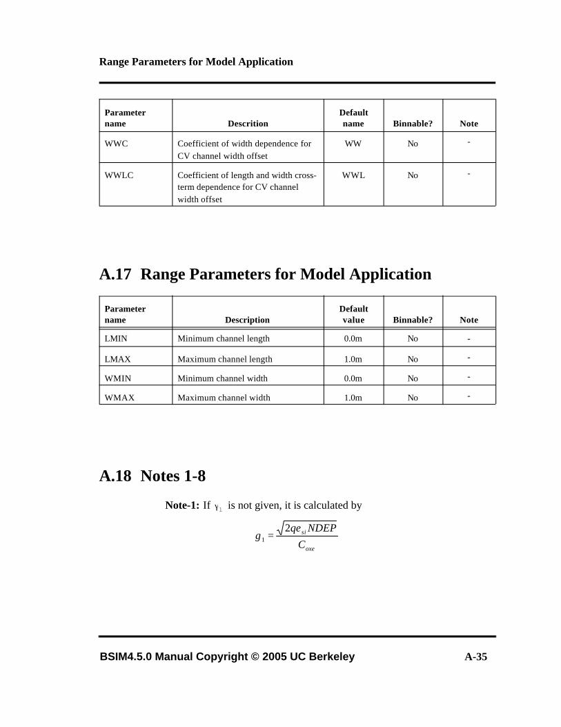
Range Parameters for Model Application
BSIM4.5.0 Manual Copyright © 2005 UC Berkeley A-35
A.17 Range Parameters for Model Application
A.18 Notes 1-8
Note-1: If is not given, it is calculated by
WWC Coefficient of width dependence for CV channel width offset
WW No -
WWLC Coefficient of length and width cross-term dependence for CV channel width offset
WWL No -
Parameter name Description
Default value Binnable? Note
LMIN Minimum channel length 0.0m No -
LMAX Maximum channel length 1.0m No -
WMIN Minimum channel width 0.0m No -
WMAX Maximum channel width 1.0m No -
Parameter name Descrition
Default name Binnable? Note
γ1
oxe
si
CNDEPqε
γ2
1 =
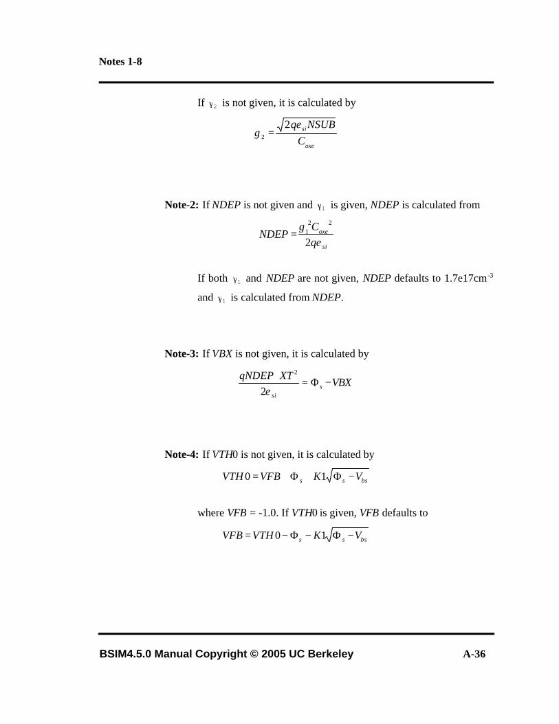
Notes 1-8
BSIM4.5.0 Manual Copyright © 2005 UC Berkeley A-36
If is not given, it is calculated by
Note-2: If NDEP is not given and is given, NDEP is calculated from
If both and NDEP are not given, NDEP defaults to 1.7e17cm-3
and is calculated from NDEP.
Note-3: If VBX is not given, it is calculated by
Note-4: If VTH0 is not given, it is calculated by
where VFB = -1.0. If VTH0 is given, VFB defaults to
γ2
oxe
si
CNSUBqε
γ2
2 =
γ1
si
oxe
qC
NDEPε
γ2
221=
γ1
γ1
VBXXTqNDEP
ssi
−Φ=⋅
ε2
2
bsss VKVFBVTH −Φ+Φ+= 10
bsss VKVTHVFB −Φ−Φ−= 10
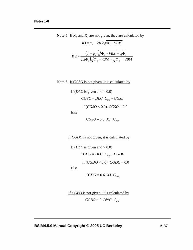
Notes 1-8
BSIM4.5.0 Manual Copyright © 2005 UC Berkeley A-37
Note-5: If K1 and K2 are not given, they are calculated by
Note-6: If CGSO is not given, it is calculated by
If (DLC is given and > 0.0)
if (CGSO < 0.0), CGSO = 0.0Else
If CGDO is not given, it is calculated by
If (DLC is given and > 0.0)
if (CGDO < 0.0), CGDO = 0.0Else
If CGBO is not given, it is calculated by
VBMKK s −Φ−= 221 2γ
( )( )( ) VBMVBM
VBXK
sss
ss
+Φ−−ΦΦ
Φ−−Φ−=
22 21 γγ
CGSLCDLCCGSO oxe −⋅=
oxeCXJCGSO ⋅⋅= 6.0
CGDLCDLCCGDO oxe −⋅=
oxeCXJCGDO ⋅⋅= 6.0
oxeCDWCCGBO ⋅⋅= 2
Notes 1-8
BSIM4.5.0 Manual Copyright © 2005 UC Berkeley A-38
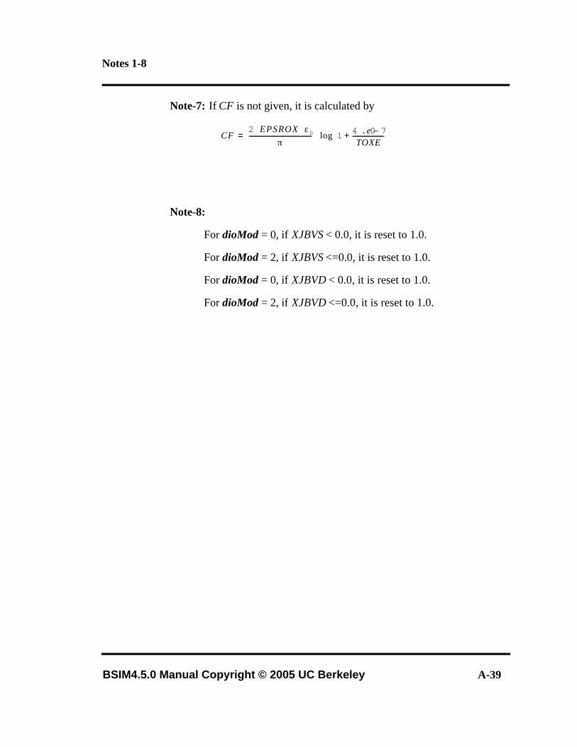
Notes 1-8
BSIM4.5.0 Manual Copyright © 2005 UC Berkeley A-39
Note-7: If CF is not given, it is calculated by
Note-8:
For dioMod = 0, if XJBVS < 0.0, it is reset to 1.0.
For dioMod = 2, if XJBVS <=0.0, it is reset to 1.0.
For dioMod = 0, if XJBVD < 0.0, it is reset to 1.0.
For dioMod = 2, if XJBVD <=0.0, it is reset to 1.0.
CF2 EPSROX ε0⋅ ⋅
π---------------------------------------- 1 4.0 e 7–
TOXE---------------------+
log⋅=
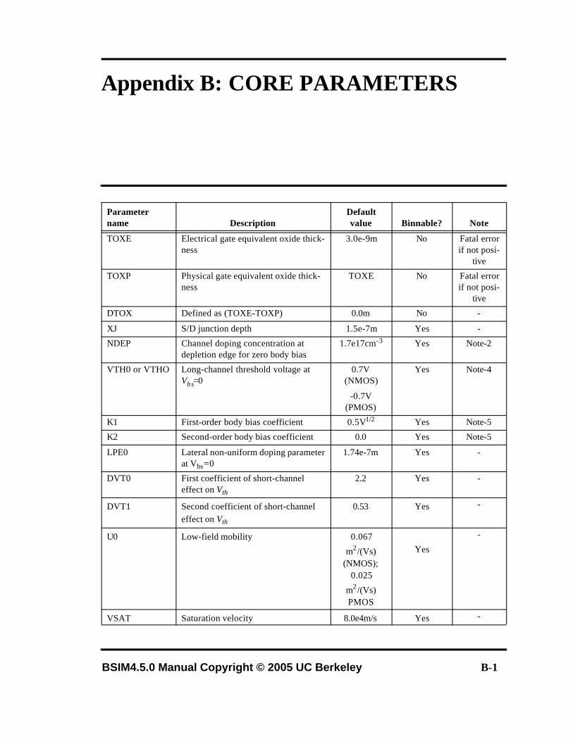
BSIM4.5.0 Manual Copyright © 2005 UC Berkeley B-1
Appendix B: CORE PARAMETERS
Parameter name Description
Default value Binnable? Note
TOXE Electrical gate equivalent oxide thick-ness
3.0e-9m No Fatal error if not posi-
tive
TOXP Physical gate equivalent oxide thick-ness
TOXE No Fatal error if not posi-
tive
DTOX Defined as (TOXE-TOXP) 0.0m No -
XJ S/D junction depth 1.5e-7m Yes -
NDEP Channel doping concentration at depletion edge for zero body bias
1.7e17cm-3 Yes Note-2
VTH0 or VTHO Long-channel threshold voltage at Vbs=0
0.7V (NMOS)
-0.7V (PMOS)
Yes Note-4
K1 First-order body bias coefficient 0.5V1/2 Yes Note-5
K2 Second-order body bias coefficient 0.0 Yes Note-5
LPE0 Lateral non-uniform doping parameter at Vbs=0
1.74e-7m Yes -
DVT0 First coefficient of short-channel effect on Vth
2.2 Yes -
DVT1 Second coefficient of short-channel effect on Vth
0.53 Yes -
U0 Low-field mobility 0.067
m2/(Vs) (NMOS);
0.025
m2/(Vs) PMOS
Yes
-
VSAT Saturation velocity 8.0e4m/s Yes -
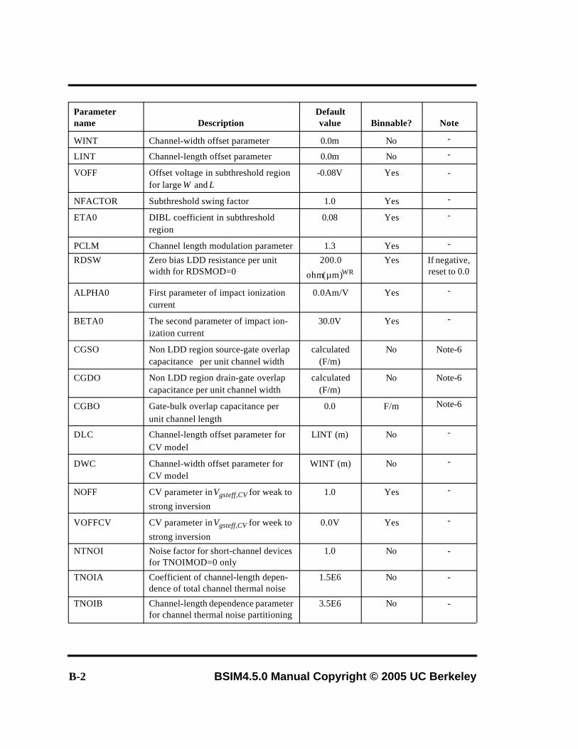
B-2 BSIM4.5.0 Manual Copyright © 2005 UC Berkeley
WINT Channel-width offset parameter 0.0m No -
LINT Channel-length offset parameter 0.0m No -
VOFF Offset voltage in subthreshold region for large W and L
-0.08V Yes -
NFACTOR Subthreshold swing factor 1.0 Yes -
ETA0 DIBL coefficient in subthreshold region
0.08 Yes -
PCLM Channel length modulation parameter 1.3 Yes -
RDSW Zero bias LDD resistance per unit width for RDSMOD=0
200.0
ohm(µm)WR
Yes If negative, reset to 0.0
ALPHA0 First parameter of impact ionization current
0.0Am/V Yes -
BETA0 The second parameter of impact ion-ization current
30.0V Yes -
CGSO Non LDD region source-gate overlap capacitance per unit channel width
calculated (F/m)
No Note-6
CGDO Non LDD region drain-gate overlap capacitance per unit channel width
calculated(F/m)
No Note-6
CGBO Gate-bulk overlap capacitance per unit channel length
0.0 F/m Note-6
DLC Channel-length offset parameter for CV model
LINT (m) No -
DWC Channel-width offset parameter for CV model
WINT (m) No -
NOFF CV parameter in Vgsteff,CV for weak to
strong inversion
1.0 Yes -
VOFFCV CV parameter in Vgsteff,CV for week to
strong inversion
0.0V Yes -
NTNOI Noise factor for short-channel devices for TNOIMOD=0 only
1.0 No -
TNOIA Coefficient of channel-length depen-dence of total channel thermal noise
1.5E6 No -
TNOIB Channel-length dependence parameter for channel thermal noise partitioning
3.5E6 No -
Parameter name Description
Default value Binnable? Note
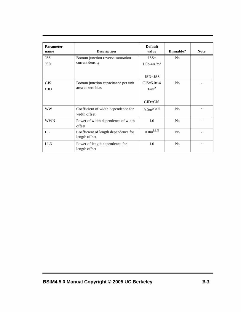
BSIM4.5.0 Manual Copyright © 2005 UC Berkeley B-3
JSS
JSD
Bottom junction reverse saturation current density
JSS=
1.0e-4A/m2
JSD=JSS
No -
CJS
CJD
Bottom junction capacitance per unit area at zero bias
CJS=5.0e-4
F/m2
CJD=CJS
No -
WW Coefficient of width dependence for width offset
0.0mWWN No -
WWN Power of width dependence of width offset
1.0 No -
LL Coefficient of length dependence for length offset
0.0mLLN No -
LLN Power of length dependence for length offset
1.0 No -
Parameter name Description
Default value Binnable? Note
BSIM4.5.0 Manual Copyright © 2005 UC Berkeley C-1
Appendix C: References
[1] Y. C. King, H. Fujioka, S. Kamohara, K. Chen, and Chenming Hu, “DC electrical oxide thickness model
for quantization of the inversion layer in MOSFETs”, Semicond. Sci. Technol., vol. 13, pp. 963-966, 1998.
[2] Weidong Liu, Xiaodong Jin, Yachin King, and Chenming Hu, “An efficient and accurate compact model
for thin-oxide-MOSFET intrinsic capacitance considering the finite charge layer thickness”, IEEE Trans.
Electron Devices, vol. ED-46, May, 1999.
[3] Kanyu M. Cao, Weidong Liu, Xiaodong Jin, Karthik Vasanth, Keith Green, John Krick, Tom Vrotsos,
and Chenming Hu, “Modeling of pocket implanted MOSFETs for anomalous analog behavior,” Tech.
Dig. of IEDM , pp. 171-174, 1999.
[4] Z.H. Liu, C. Hu, J.H. Huang, T.Y. Chan, M.C. Jeng, P.K. Ko, and Y.C. Cheng,“Threshold Voltage
Model For Deep-Submicrometer MOSFETs,” IEEE Tran. Electron Devices , vol. 40, pp. 86-95, 1993.
[5] J.A. Greenfield and R.W. Dutton, “Nonplanar VLSI Device Analysis Using the Solution of Poisson's
Equation,” IEEE Trans. Electron Devices, vol. ED-27, p.1520, 1980.
[6] H. S. Lee, “An Analysis of the Threshold Voltage for Short-Channel IGFET's,” Solid-State Electronics ,
vol.16, p.1407, 1973.
[7] Yuhua Cheng and Chenming Hu, “MOSFET Modeling & BSIM3 User’s Guide,” Kluwer Academic
Publishers, 1999.
[8] C. Hu, S. Tam, F.C. Hsu, P.K. Ko, T.Y. Chan and K.W. Kyle, "Hot-Electron Induced MOSFET
Degradation - Model, Monitor, Improvement," IEEE Trans. Electron Devices, vol. 32, pp. 375-385, 1985.
[9] T. Y. Chen, J. Chen, P. K. Ko, C. Hu, “The impact of gate-induced drain leakage current on MOSFET
scaling,” Tech. Digest of IEDM, pp. 718-721, 1987.
C-2 BSIM4.5.0 Manual Copyright © 2005 UC Berkeley
[10] S. A. Parke, E. Moon, H-J. Wenn, P. K. Ko, and C. Hu, “Design for suppression of gate-induced drain
leakage in LDD MOSFETs using a quasi 2D analytical model,” IEEE Trans. Electron Devices, vol. 39,
no. 7, pp 1694-1703, 1992.
[11] Weidong Liu, Xiaodong Jin, J. Chen, M. Jeng, Z. Liu, Y. Cheng, K. Chen, M. Chan, K. Hui, J. Huang,
R. Tu, P. Ko, and Chenming Hu, “BSIM3v3.2 MOSFET Model and Users’ Manual,” http://www-
device.eecs.berkeley.edu/~bsim3.
[12] Xiaodong Jin, J-J Ou, C-H Chen, Weidong Liu, Paul Gray, and Chenming Hu, “An effective gate
resistance model for CMOS RF and noise modeling,” Tech. Dig. of IEDM, pp. 961-964, 1998.
[13] Mansun Chan, K. Hui, R. Neff, C. Hu, P. Ko, “A Relaxation time Approach to Model the Non-Quasi-
Static Transient Effects in MOSFETs,” Tech. Dig. of IEDM , pp. 169-172, 1994.
[14] K.K. Hung, P. Ko, C. Hu, and Y. C. Cheng, “A Physics-Based MOSFET Noise Model for Circuit
Simulators,” IEEE Trans. Electron Devices , vol. 37, no. 5, pp. 1323-1333, 1990.
[15] Weidong Liu, Kanyu M. Cao, Xiaodong Jin, and Chenming Hu, “BSIM4.0.0 Technical Notes,” http://
www-device.eecs.berkeley.edu/~bsim3/bsim4.html.
[16] R.A.Bianchi, G.Bouche and O.Roux-dit-Buisson, "Accurate Modeling of Trench Isolation Induced
Mechanical Stress Effect on MOSFET Electrical Performance," IEDM 2002, pp. 117-120.
[17] Hook, T.B.; Brown, J.; Cottrell, P.; Adler, E.; Hoyniak, D.; Johnson, J.; Mann, R., “Lateral ion implant
straggle and mask proximity effect”, IEEE Trans. Electron Devices , Volume 50, no 9, pp 1946- 1951,
Sept. 2003
[18] Yi-Ming Sheu, Ke-Wei Su, Sheng-Jier Yang, Hsien-Te Chen, Chih-Chiang Wang, Ming-Jer Chen, and
Sally Liu, “Modeling Well Edge Proximity Effect on Highly-Scaled MOSFETs”, CICC 2005