Embed Size (px)
Citation preview
Broadband absorption and efficiency
enhancement of an ultra-thin silicon solar cell
with a plasmonic fractal
Li-Hao Zhu,1 Ming-Rui Shao,
1 Ru-Wen Peng,
1,* Ren-Hao Fan,
1
Xian-Rong Huang,2 and Mu Wang
1
1National Laboratory of Solid State Microstructures and Department of Physics, Nanjing University, Nanjing 210093,
China 2Advanced Photon Source, Argonne National Laboratory, Argonne, Illinois 60439, USA
Abstract: We report in this work that quantum efficiency can be
significantly enhanced in an ultra-thin silicon solar cell coated by a
fractal-like pattern of silver nano cuboids. When sunlight shines this solar
cell, multiple antireflection bands are achieved mainly due to the
self-similarity in the fractal-like structure. Actually, several kinds of optical
modes exist in the structure. One is cavity modes, which come from
Fabry-Perot resonances at the longitudinal and transverse cavities,
respectively; the other is surface plasmon (SP) modes, which propagate
along the silicon-silver interface. Due to the fact that several feature sizes
distribute in a fractal-like structure, both low-index and high-index SP
modes are simultaneously excited. As a whole effect, broadband absorption
is achieved in this solar cell. Further by considering the ideal process that the
lifetime of carriers is infinite and the recombination loss is ignored, we
demonstrate that external quantum efficiency of the solar cell under this
ideal condition is significantly enhanced. This theoretical finding
contributes to high-performance plasmonic solar cells and can be applied to
designing miniaturized compact photovoltaic devices.
©2013 Optical Society of America
OCIS codes: (250.5403) Plasmonics; (040.5350) Photovoltaic; (350.6050) Solar energy.
References and links
1. M. A. Green, K. Emery, Y. Hishikawa, and W. Warta, “Solar cell efficiency tables (Version 37),” Prog. Photovolt.
Res. Appl. 19(1), 84–92 (2011). 2. H. A. Atwater and A. Polman, “Plasmonics for improved photovoltaic devices,” Nat. Mater. 9(3), 205–213
(2010).
3. M. A. Green, “Recent developments in photovoltaics,” Sol. Energy 76(1–3), 3–8 (2004). 4. V. E. Ferry, M. A. Verschuuren, H. B. T. Li, E. Verhagen, R. J. Walters, R. E. I. Schropp, H. A. Atwater, and A.
Polman, “Light trapping in ultrathin plasmonic solar cells,” Opt. Express 18(13, S2), A237–A245 (2010).
5. L. L. Ma, Y. C. Zhou, N. Jiang, X. Lu, J. Shao, W. Lu, J. Ge, X. M. Ding, and X. Y. Hou, “Wide-band “black
silicon” based on porous silicon,” Appl. Phys. Lett. 88(17), 171907 (2006).
6. C. A. Keasler and E. Bellotti, “A numerical study of broadband absorbers for visible to infrared detectors,” Appl.
Phys. Lett. 99(9), 091109 (2011). 7. Y. J. Lee, D. S. Ruby, D. W. Peters, B. B. McKenzie, and J. W. P. Hsu, “ZnO nanostructures as efficient
antireflection layers in solar cells,” Nano Lett. 8(5), 1501–1505 (2008).
8. S. Fahr, T. Kirchartz, C. Rockstuhl, and F. Lederer, “Approaching the Lambertian limit in randomly textured thin-film solar cells,” Opt. Express 19(14, S4), A865–A874 (2011).
9. S. A. Maier, P. G. Kik, H. A. Atwater, S. Meltzer, E. Harel, B. E. Koel, and A. A. G. Requicha, “Local detection
of electromagnetic energy transport below the diffraction limit in metal nanoparticle plasmon waveguides,” Nat. Mater. 2(4), 229–232 (2003).
10. S. Chhajed, M. F. Schubert, J. K. Kim, and E. F. Schubert, “Nanostructured multilayer graded-index antireflection
coating for Si solar cells with broadband and omnidirectional characteristics,” Appl. Phys. Lett. 93(25), 251108 (2008).
#184209 - $15.00 USD Received 25 Jan 2013; revised 10 Mar 2013; accepted 11 Mar 2013; published 19 Mar 2013(C) 2013 OSA 6 May 2013 / Vol. 21, No. S3 / OPTICS EXPRESS A313
11. J. F. Zhu, M. Xue, H. J. Shen, Z. Wu, S. Kim, J. J. Ho, A. Hassani-Afshar, B. Q. Zeng, and K. L. Wang,
“Plasmonic effects for light concentration in organic photovoltaic thin films induced by hexagonal periodic metallic nanospheres,” Appl. Phys. Lett. 98(15), 151110 (2011).
12. Y. N. Zhang, Z. Ouyang, N. Stokes, B. H. Jia, Z. R. Shi, and M. Gu, “Low cost and high performance Al
nanoparticles for broadband light trapping in Si wafer solar cells,” Appl. Phys. Lett. 100(15), 151101 (2012). 13. Y. H. Kuang, K. H. M. van der Werf, Z. S. Houweling, and R. E. I. Schropp, “Nanorod solar cell with an ultrathin
a-Si:H absorber layer,” Appl. Phys. Lett. 98(11), 113111 (2011).
14. H. P. Wang, K. T. Tsai, K. Y. Lai, T. C. Wei, Y. L. Wang, and J. H. He, “Periodic Si nanopillar arrays by anodic aluminum oxide template and catalytic etching for broadband and omnidirectional light harvesting,” Opt. Express
20(S1), A94–A103 (2012).
15. R. A. Pala, J. White, E. Barnard, J. Liu, and M. L. Brongersma, “Design of Plasmonic Thin-Film Solar Cells with Broadband Absorption Enhancements,” Adv. Mater. 21(34), 3504–3509 (2009).
16. E. Battal, T. A. Yogurt, L. E. Aygun, and A. K. Okyay, “Triangular metallic gratings for large absorption
enhancement in thin film Si solar cells,” Opt. Express 20(9), 9458–9464 (2012). 17. A. Abass, K. Q. Le, A. Alu, M. Burgelman, and B. Maes, “Dual-interface gratings for broadband absorption
enhancement in thin-film solar cells,” Phys. Rev. B 85(11), 115449 (2012).
18. B. B. Mandelbrot, The Fractal Geometry of Nature (W. H. Freeman, 1982).
19. Y. J. Bao, B. Zhang, Z. Wu, J. W. Si, M. Wang, R. W. Peng, X. Lu, J. Shao, Z. F. Li, X. P. Hao, and N. B. Ming,
“Surface-plasmon-enhanced transmission through metallic film perforated with fractal-featured aperture array,”
Appl. Phys. Lett. 90(25), 251914 (2007). 20. G. Volpe, G. Volpe, and R. Quidant, “Fractal plasmonics: subdiffraction focusing and broadband spectral
response by a Sierpinski nanocarpet,” Opt. Express 19(4), 3612–3618 (2011).
21. O. Vetterl, F. Finger, R. Carius, P. Hapke, L. Houben, O. Kluth, A. Lambertz, A. Muck, B. Rech, and H. Wagner, “Intrinsic microcrystalline silicon: A new material for photovoltaics,” Sol. Energy Mater. Sol. Cells 62(1–2),
97–108 (2000).
22. E. D. Palik, Handbook of Optical Constants of Solids (Academic, 1985). 23. W. L. Barnes, A. Dereux, and T. W. Ebbesen, “Surface plasmon subwavelength optics,” Nature 424(6950),
824–830 (2003). 24. D. Li, L. Qin, X. Xiong, R. W. Peng, Q. Hu, G. B. Ma, H. S. Zhou, and M. Wang, “Exchange of electric and
magnetic resonances in multilayered metal/dielectric nanoplates,” Opt. Express 19(23), 22942–22949 (2011).
25. M. Yang, Z. P. Fu, F. Lin, and X. Zhu, “Incident angle dependence of absorption enhancement in plasmonic solar cells,” Opt. Express 19(S4), A763–A771 (2011).
26. Z. H. Tang, R. W. Peng, Z. Wang, X. Wu, Y. J. Bao, Q. J. Wang, Z. J. Zhang, W. H. Sun, and M. Wang, “Coupling
of surface plasmons in nanostructured metal/dielectric multilayers with subwavelength hole arrays,” Phys. Rev. B
76(19), 195405 (2007).
27. J. N. Munday and H. A. Atwater, “Large Integrated Absorption Enhancement in Plasmonic Solar Cells by
Combining Metallic Gratings and Antireflection Coatings,” Nano Lett. 11(6), 2195–2201 (2011). 28. T. Markvart and L. Castaner, Practical handbook of photovoltaics: fundamentals and applications (Elsevier
Advanced Technology, 2003). Chap. a1.
29. W. Shockley and H. J. Queisser, “Detailed balance limit of efficiency of pn junction solar cells,” J. Appl. Phys. 32(3), 510 (1961).
30. R. W. Peng, M. Mazzer, and K. W. J. Barnham, “Efficiency enhancement of ideal photovoltaic solar cells by
photonic excitations in multi-intermediate band structures,” Appl. Phys. Lett. 83(4), 770–772 (2003). 31. B. C. P. Sturmberg, K. B. Dossou, L. C. Botten, A. A. Asatryan, C. G. Poulton, C. M. de Sterke, and R. C.
McPhedran, “Modal analysis of enhanced absorption in silicon nanowire arrays,” Opt. Express 19(S5),
A1067–A1081 (2011). 32. ASTM G173 – 03, “Standard tables for reference solar spectral irradiances” (2012),
http://www.astm.org/Standards/G173.htm.
33. A. Wang, J. Zhao, and M. A. Green, “24% efficient silicon solar cells,” Appl. Phys. Lett. 57(6), 602–604 (1990).
1. Introduction
Silicon is always the leading material in low-cost commercial solar cells, for its second
abundance on earth and non-toxicity in production. Increasing power conversion efficiency
and reducing manufacture cost are important keys to high-performance solar cells [1]. But for
further improving the efficiency, the main problem of silicon material is that the absorption
length (>2000nm) is much longer than the excitation diffusion length (<100nm) [2]. In the past
decades, the second-generation thin-film solar cells [3] have offered a viable pathway to solve
this problem by reducing the carrier recombination in the bulk of semiconductor. Yet the
efficiency of thin-film solar cells is still not high enough comparing with traditional
thick-wafer ones.
#184209 - $15.00 USD Received 25 Jan 2013; revised 10 Mar 2013; accepted 11 Mar 2013; published 19 Mar 2013(C) 2013 OSA 6 May 2013 / Vol. 21, No. S3 / OPTICS EXPRESS A314
It is known that antireflection coatings (ARC) are applied to inhibit light reflecting into the
air [4–7], such as randomly textured surfaces [7] and graded refractive-index surfaces [8].
Recently, it has been found that the efficiency can be enhanced in a plasmonic way [2,9–17].
For example, metallic core-shell nanoparticles [11,12], highly ordered nanorods and
nanopillars [13,14], e.g. are promising approaches for enhancement. In addition, metallic
nanogratings locating on the top [15], the bottom [16] and both sides [17] of solar cells can lead
to high efficiency, respectively. In all of these ways, broadband absorption is a promising
concept perused by the researchers. Physically, if the absorption to sunlight irradiation is
extended to in broader bandwidths, more previously-wasted solar energy can be collected and
converted into photocurrents, which finally enhancing the efficiency of solar cells. Though
much progress has been made on this aspect, lots of solar cell systems achieve strong
absorption only in narrowband, and so far it is still not fully investigated about broadband
absorption enhancement in ultra-thin film photovoltaic (PV) devices.
In this work, in order to achieve broadband enhancement, we design a fractal-like pattern
of silver nano cuboids on the top of an ultra-thin silicon solar cell. Based on the
three-dimensional (3D) finite-difference time-domain (FDTD) method, we show theoretically
that by introducing multiple length scales within the same structure (i.e., fractal), multiple
momentum compensations are achieved in the system. Then incident light at different
frequency bands can couple into the cavity modes and the surface plasmon modes,
respectively. In this way, broadband absorption and efficiency enhancement are achieved in
this system. This finding contributes to high-performance plasmonic solar cells and can be
applied to design miniaturized compact photovoltaic devices.
2. The proposed structure and the simulation method
The concept of fractal can trace back to 17th century, but the term “fractal” was first used by
mathematician Benoît Mandelbrot, now fractal is famous for its self-similar patterns at
different scales and outstanding characteristics [18]. Some groups (including ours) have
already employed fractal to the plasmonic nanostructures [19,20]. Here we further extend this
idea to the photovoltaic devices and try to improve the solar cell efficiency. In order to achieve
broadband response of electromagnetic waves, we intentionally design a fractal-like pattern of
silver nano cuboids coated on an ultra-thin silicon solar cell. As shown in Fig. 1, the system
contains three layers: a silver (Ag) fractal-like pattern (thickness d1) coated on the top, a
crystalline silicon (c-Si) absorb layer (thickness d2) in the middle and a silver (Ag) back
reflector (thickness d3) on the bottom. Here we do not give the dielectric anti-reflection coating
(ARC) and the passivation layer in this simplified system, but in Sec. 3 we additionally show
the role of dielectric ARC in the device. The plasmonic fractal can be constructed as follow. It
starts from the original period (P) with a central square pattern and then it is divided into a grid
of 2 × 2. In each sub-period (0.5P), a sub-square pattern is also in the center. On every next
scale, it repeats the same operation. For several times of iterations, we can illustrate this
fractal-like pattern on top left inset in Fig. 1. Besides, the back reflector is needed in order to
reflect the incident light back and extends the absorption thickness, especially in ultra-thin PV
devices [21]. Two reference structures are given: one is a free-standing 50nm-thick Si film
(ref-1) and the other is a 50nm-thick Si film on the top of a 250nm-thick Ag back reflector
(ref-2).
#184209 - $15.00 USD Received 25 Jan 2013; revised 10 Mar 2013; accepted 11 Mar 2013; published 19 Mar 2013(C) 2013 OSA 6 May 2013 / Vol. 21, No. S3 / OPTICS EXPRESS A315
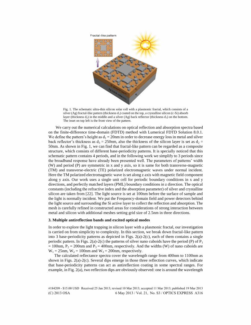
Fig. 1. The schematic ultra-thin silicon solar cell with a plasmonic fractal, which consists of a
silver (Ag) fractal-like pattern (thickness d1) coated on the top, a crystalline silicon (c-Si) absorb
layer (thickness d2) in the middle and a silver (Ag) back reflector (thickness d3) on the bottom. The inset on top left is the front view of the pattern.
We carry out the numerical calculations on optical reflection and absorption spectra based
on the finite-difference time-domain (FDTD) method with Lumerical FDTD Solution 8.0.1.
We define the pattern’s height as d1 = 20nm in order to decrease energy loss in metal and silver
back reflector’s thickness as d3 = 250nm, also the thickness of the silicon layer is set as d2 =
50nm. As shown in Fig. 1, we can find that fractal-like pattern can be regarded as a composite
structure, which consists of different base-periodicity patterns. It is specially noticed that this
schematic pattern contains 4 periods, and in the following work we simplify to 3 periods since
the broadband response have already been presented well. The parameters of patterns’ width
(W) and period (P) are symmetric in x and y axis, so it is same for both transverse-magnetic
(TM) and transverse-electric (TE) polarized electromagnetic waves under normal incident.
Here the TM polarized electromagnetic wave is set along z axis with magnetic field component
along y axis. Our work uses a single unit cell for periodic boundary conditions in x and y
directions, and perfectly matched layers (PML) boundary conditions in z direction. The optical
constants (including the refractive index and the absorption parameter) of silver and crystalline
silicon are taken from [22]. The light source is set at 100nm before the surface of sample and
the light is normally incident. We put the Frequency-domain field and power detectors behind
the light source and surrounding the Si active layer to collect the reflection and absorption. The
mesh is carefully refined in constructed areas for considerations of strong interaction between
metal and silicon with additional meshes setting grid size of 2.5nm in three directions.
3. Multiple antireflection bands and excited optical modes
In order to explore the light trapping in silicon layer with a plasmonic fractal, our investigation
is carried on from simplicity to complexity. In this section, we break down fractal-like pattern
into 3 base-periodicity patterns as depicted in Figs. 2(a)-2(c), each of them contains a single
periodic pattern. In Figs. 2(a)-2(c) the patterns of silver nano cuboids have the period (P) of P1
= 100nm, P2 = 200nm and P3 = 400nm, respectively. And the widths (W) of nano cuboids are
W1 = 25nm, W2 = 100nm and W3 = 200nm, respectively.
The calculated reflectance spectra cover the wavelength range from 400nm to 1100nm as
shown in Figs. 2(a)-2(c). Several dips emerge in those three reflection curves, which indicate
that base-periodicity patterns can act as antireflection coating in some spectral ranges. For
example, in Fig. 2(a), two reflection dips are obviously observed: one is around the wavelength
#184209 - $15.00 USD Received 25 Jan 2013; revised 10 Mar 2013; accepted 11 Mar 2013; published 19 Mar 2013(C) 2013 OSA 6 May 2013 / Vol. 21, No. S3 / OPTICS EXPRESS A316
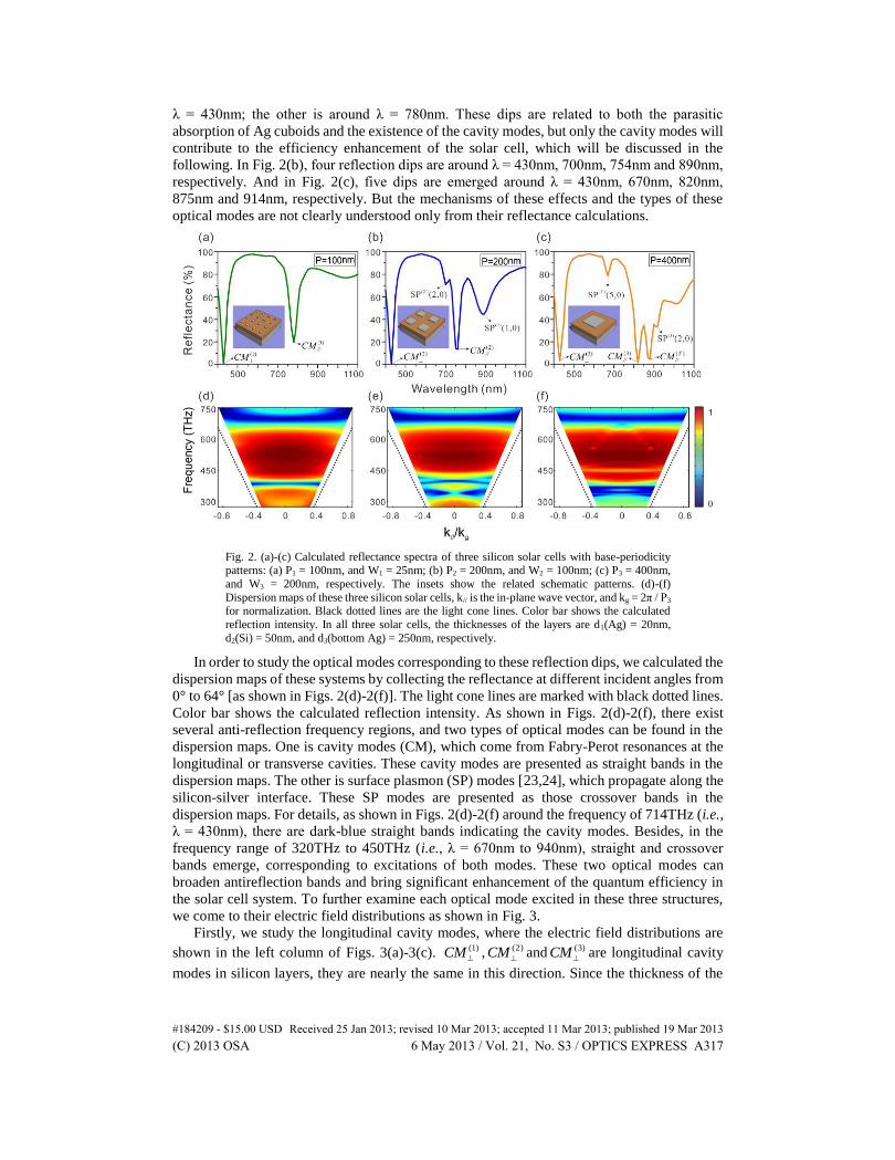
λ = 430nm; the other is around λ = 780nm. These dips are related to both the parasitic
absorption of Ag cuboids and the existence of the cavity modes, but only the cavity modes will
contribute to the efficiency enhancement of the solar cell, which will be discussed in the
following. In Fig. 2(b), four reflection dips are around λ = 430nm, 700nm, 754nm and 890nm,
respectively. And in Fig. 2(c), five dips are emerged around λ = 430nm, 670nm, 820nm,
875nm and 914nm, respectively. But the mechanisms of these effects and the types of these
optical modes are not clearly understood only from their reflectance calculations.
Fig. 2. (a)-(c) Calculated reflectance spectra of three silicon solar cells with base-periodicity
patterns: (a) P1 = 100nm, and W1 = 25nm; (b) P2 = 200nm, and W2 = 100nm; (c) P3 = 400nm,
and W3 = 200nm, respectively. The insets show the related schematic patterns. (d)-(f)
Dispersion maps of these three silicon solar cells, k// is the in-plane wave vector, and kg = 2π / P3 for normalization. Black dotted lines are the light cone lines. Color bar shows the calculated
reflection intensity. In all three solar cells, the thicknesses of the layers are d1(Ag) = 20nm,
d2(Si) = 50nm, and d3(bottom Ag) = 250nm, respectively.
In order to study the optical modes corresponding to these reflection dips, we calculated the
dispersion maps of these systems by collecting the reflectance at different incident angles from
0° to 64° [as shown in Figs. 2(d)-2(f)]. The light cone lines are marked with black dotted lines.
Color bar shows the calculated reflection intensity. As shown in Figs. 2(d)-2(f), there exist
several anti-reflection frequency regions, and two types of optical modes can be found in the
dispersion maps. One is cavity modes (CM), which come from Fabry-Perot resonances at the
longitudinal or transverse cavities. These cavity modes are presented as straight bands in the
dispersion maps. The other is surface plasmon (SP) modes [23,24], which propagate along the
silicon-silver interface. These SP modes are presented as those crossover bands in the
dispersion maps. For details, as shown in Figs. 2(d)-2(f) around the frequency of 714THz (i.e.,
λ = 430nm), there are dark-blue straight bands indicating the cavity modes. Besides, in the
frequency range of 320THz to 450THz (i.e., λ = 670nm to 940nm), straight and crossover
bands emerge, corresponding to excitations of both modes. These two optical modes can
broaden antireflection bands and bring significant enhancement of the quantum efficiency in
the solar cell system. To further examine each optical mode excited in these three structures,
we come to their electric field distributions as shown in Fig. 3.
Firstly, we study the longitudinal cavity modes, where the electric field distributions are
shown in the left column of Figs. 3(a)-3(c). (1)CM , (2)CM and (3)CM are longitudinal cavity
modes in silicon layers, they are nearly the same in this direction. Since the thickness of the
#184209 - $15.00 USD Received 25 Jan 2013; revised 10 Mar 2013; accepted 11 Mar 2013; published 19 Mar 2013(C) 2013 OSA 6 May 2013 / Vol. 21, No. S3 / OPTICS EXPRESS A317
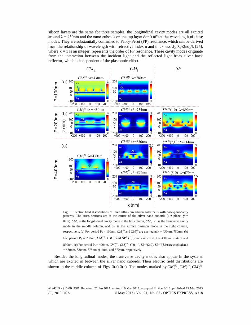
silicon layers are the same for three samples, the longitudinal cavity modes are all excited
around λ = 430nm and the nano cuboids on the top layer don’t affect the wavelength of these
modes. They are substantially confirmed to Fabry-Perot (FP) resonance, which can be derived
from the relationship of wavelength with refractive index n and thickness d2, λk2nd2/k [25],
where k = 1 is an integer, represents the order of FP resonance. These cavity modes originate
from the interaction between the incident light and the reflected light from silver back
reflector, which is independent of the plasmonic effect.
Fig. 3. Electric field distributions of three ultra-thin silicon solar cells with base-periodicity patterns. The cross sections are at the center of the silver nano cuboids (x-z plane, y =
0nm). CM
is the longitudinal cavity mode in the left column, CM ∥
�is the transverse cavity
mode in the middle column, and SP is the surface plasmon mode in the right column,
respectively. (a) For period P1 = 100nm,(1)
CM
and(1)
CM∥
are excited at λ = 430nm, 780nm. (b)
For period P2 = 200nm,( 2 )
CM
,( 2 )
CM∥
and SP(2)(1,0) are excited at λ = 430nm, 754nm and
890nm. (c) For period P3 = 400nm,(3)
CM
,(3)
CM∥
,(3 ')
CM∥
, SP(3)(2,0), SP(3)(5,0) are excited at λ
= 430nm, 820nm, 875nm, 914nm, and 670nm, respectively.
Besides the longitudinal modes, the transverse cavity modes also appear in the system,
which are excited in between the silver nano cuboids. Their electric field distributions are
shown in the middle column of Figs. 3(a)-3(c). The modes marked by (1)CM∥ , (2)CM∥ , (3)CM∥
#184209 - $15.00 USD Received 25 Jan 2013; revised 10 Mar 2013; accepted 11 Mar 2013; published 19 Mar 2013(C) 2013 OSA 6 May 2013 / Vol. 21, No. S3 / OPTICS EXPRESS A318
and ’(3 )CM∥ correspond to the transverse cavity modes at λ = 780nm (P1), 754nm (P2), 820nm
(P3) and 875nm (P3) respectively. Taking the mode “ (1)CM∥ ” as an example, we can see that
strong electric fields are mainly confined in the silicon layer and its surrounding cuboids; and
the electric fields around the cuboids can interact with those in neighbor cuboids along the
parallel direction, which verify the resonance in the transverse cavity. Similarly, (2)CM∥ has the
same mechanism and the electric fields are more confined in the active layer than those in the
silver nano cuboids. To be noticed, (3)CM∥ and ’(3 )CM∥ are the high-index transverse cavity
modes, which are not excited between the neighbors but inside its own period. Compared with
the mode of (3)CM∥ , the mode of ’(3 )CM∥ has stronger electric fields and its electromagnetic
energies are more confined in the active layer [as shown in Fig. 3]. These modes play an
important role in the enhancement of solar cell’s efficiency, since their electric fields are
mainly confined in the active layer, and their intensities are considerably strong.
Actually surface plasmon (SP) modes are also excited in the system, which originate from
the interaction between the surface charge oscillation and the electromagnetic field of the light.
Since the SP can be tailored by adjusting the subwavelength structures on metal surface, such
as altering the type of the structure and the geometry of the unit cell, it may offer a prominent
way for absorption enhancement in our solar cell system. It is well known that at the interface
separating a metal and a dielectric, the SP mode obeys the dispersion relation as [23]
0 ,d m
SP
d m
k k
(1)
where kSP is the wave vector of the SP, k0 is the in-plane component of the incident wave
vector and εd and εm are permittivity of dielectric and metal. We also obtain the minimum
reflectance λmin satisfying [26]:
min2 2
.+
d m
d m
P
i j
(2)
From Eq. (2) the crossover bands around reflectance dips can be indexed with integers (i,j) in
the optical spectra [as shown in Figs. 2(a)-2(c)]. In every base-periodicity pattern, momentum
conservations are strictly required. Electric field distributions of SP modes are shown in the
right column of Figs. 3(b) and 3(c), we can see that the electric-field enhancement is between
the silicon-silver interface and the electric-field propagates along the interface. In Fig. 3(a),
there is no SP mode supported, because the period is too small to satisfy momentum
conservation. Based on our calculations, the SP modes can be indexed as SP(2)
(1,0) at λ =
890nm (P2), SP(2’)
(2,0) at λ = 700nm (P2) in Fig. 2(b), SP(3)
(2,0) at λ = 914nm (P3), and
SP(3)
(5,0) at λ = 670nm (P3) in Fig. 2(c), respectively. Therefore, we can make a conclusion
that in these solar cell systems with base-periodicity patterns, both low-index and high-index
SP modes can be simultaneously excited. And they are evidently different from cavity modes.
At the SP modes, the electromagnetic waves propagate along the silver-silicon interface and
most of electromagnetic energies can come to the active layer (silicon).
4. Broadband absorption and efficiency enhancement
Now that we can understand the optical modes excited in the plasmonic solar cell system with
base-periodicity patterns, we can draw our attentions on the absorption and the efficiency of
the solar cells. The absorbance [27] of the solar cell at a given wavelength (λ) is evaluated by
2
( ) Im( ) ,A E dV (3)
#184209 - $15.00 USD Received 25 Jan 2013; revised 10 Mar 2013; accepted 11 Mar 2013; published 19 Mar 2013(C) 2013 OSA 6 May 2013 / Vol. 21, No. S3 / OPTICS EXPRESS A319
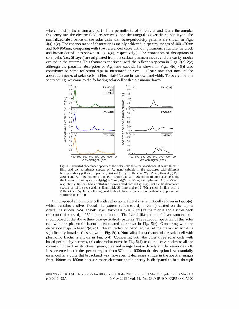
where Im(ε) is the imaginary part of the permittivity of silicon, ω and E are the angular
frequency and the electric field, respectively, and the integral is over the silicon layer. The
normalized absorbance of the solar cells with base-periodicity patterns are shown in Figs.
4(a)-4(c). The enhancement of absorption is mainly achieved in spectral ranges of 400-470nm
and 650-950nm, comparing with two referenced cases without plasmonic structure [as black
and brown dotted lines shown in Fig. 4(a), respectively.]. The resonances of absorptions of
solar cells (i.e., Si layer) are originated from the surface plasmon modes and the cavity modes
excited in the systems. This feature is consistent with the reflection spectra in Figs. 2(a)-2(c)
although the parasitic absorption of Ag nano cuboids [as shown in Figs. 4(d)-4(f)] also
contributes to some reflection dips as mentioned in Sec. 3. Please note that most of the
absorption peaks of solar cells in Figs. 4(a)-4(c) are in narrow bandwidth. To overcome this
shortcoming, we come to the following solar cell with a plasmonic fractal.
Fig. 4. Calculated absorbance spectra of the solar cells (i.e., the absorbance of 50nm thick Si film) and the absorbance spectra of Ag nano cuboids in the structures with different
base-periodicity patterns, respectively. (a) and (d) P1 = 100nm and W1 = 25nm; (b) and (e) P2 =
200nm and W2 = 100nm; (c) and (f) P3 = 400nm and W3 = 200nm. In all three solar cells, the thicknesses of the layers are d1(Ag) = 20nm, d2(Si) = 50nm, and d3(bottom Ag) = 250nm,
respectively. Besides, black-dotted and brown-dotted lines in Fig. 4(a) illustrate the absorbance
spectra of ref-1 (free-standing 50nm-thick Si film) and ref-2 (50nm-thick Si film with a 250nm-thick Ag back reflector), and both of these references are without any plasmonic
structures on the top.
Our proposed silicon solar cell with a plasmonic fractal is schematically shown in Fig. 5(a),
which contains a silver fractal-like pattern (thickness d1 = 20nm) coated on the top, a
crystalline silicon (c-Si) absorb layer (thickness d2 = 50nm) in the middle and a silver back
reflector (thickness d3 = 250nm) on the bottom. The fractal-like pattern of silver nano cuboids
is composed of the above three base-periodicity patterns. The reflection spectrum of this solar
cell with the plasmonic fractal is calculated as shown in Fig. 5(c). Comparing with the
dispersion maps in Figs. 2(d)-2(f), the antireflection band regimes of the present solar cell is
significantly broadened as shown in Fig. 5(b). Normalized absorbance of the solar cell with
plasmonic fractal is shown in Fig. 5(d). Comparing with the other three solar cells with
based-periodicity patterns, this absorption curve in Fig. 5(d) (red line) covers almost all the
curves of those three structures (green, blue and orange line) with only a little resonance shift.
It is presented that in the spectral regime from 670nm to 1000nm the absorption is substantially
enhanced in a quite flat broadband way, however, it decreases a little in the spectral ranges
from 400nm to 480nm because more electromagnetic energy is dissipated to heat through
#184209 - $15.00 USD Received 25 Jan 2013; revised 10 Mar 2013; accepted 11 Mar 2013; published 19 Mar 2013(C) 2013 OSA 6 May 2013 / Vol. 21, No. S3 / OPTICS EXPRESS A320
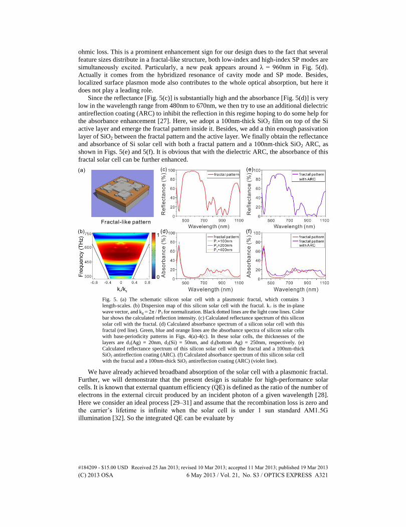
ohmic loss. This is a prominent enhancement sign for our design dues to the fact that several
feature sizes distribute in a fractal-like structure, both low-index and high-index SP modes are
simultaneously excited. Particularly, a new peak appears around λ = 960nm in Fig. 5(d).
Actually it comes from the hybridized resonance of cavity mode and SP mode. Besides,
localized surface plasmon mode also contributes to the whole optical absorption, but here it
does not play a leading role.
Since the reflectance [Fig. 5(c)] is substantially high and the absorbance [Fig. 5(d)] is very
low in the wavelength range from 480nm to 670nm, we then try to use an additional dielectric
antireflection coating (ARC) to inhibit the reflection in this regime hoping to do some help for
the absorbance enhancement [27]. Here, we adopt a 100nm-thick SiO2 film on top of the Si
active layer and emerge the fractal pattern inside it. Besides, we add a thin enough passivation
layer of SiO2 between the fractal pattern and the active layer. We finally obtain the reflectance
and absorbance of Si solar cell with both a fractal pattern and a 100nm-thick SiO2 ARC, as
shown in Figs. 5(e) and 5(f). It is obvious that with the dielectric ARC, the absorbance of this
fractal solar cell can be further enhanced.
Fig. 5. (a) The schematic silicon solar cell with a plasmonic fractal, which contains 3
length-scales. (b) Dispersion map of this silicon solar cell with the fractal. k// is the in-plane
wave vector, and kg = 2π / P3 for normalization. Black dotted lines are the light cone lines. Color bar shows the calculated reflection intensity. (c) Calculated reflectance spectrum of this silicon
solar cell with the fractal. (d) Calculated absorbance spectrum of a silicon solar cell with this
fractal (red line). Green, blue and orange lines are the absorbance spectra of silicon solar cells with base-periodicity patterns in Figs. 4(a)-4(c). In these solar cells, the thicknesses of the
layers are d1(Ag) = 20nm, d2(Si) = 50nm, and d3(bottom Ag) = 250nm, respectively. (e)
Calculated reflectance spectrum of this silicon solar cell with the fractal and a 100nm-thick SiO2 antireflection coating (ARC). (f) Calculated absorbance spectrum of this silicon solar cell
with the fractal and a 100nm-thick SiO2 antireflection coating (ARC) (violet line).
We have already achieved broadband absorption of the solar cell with a plasmonic fractal.
Further, we will demonstrate that the present design is suitable for high-performance solar
cells. It is known that external quantum efficiency (QE) is defined as the ratio of the number of
electrons in the external circuit produced by an incident photon of a given wavelength [28].
Here we consider an ideal process [29–31] and assume that the recombination loss is zero and
the carrier’s lifetime is infinite when the solar cell is under 1 sun standard AM1.5G
illumination [32]. So the integrated QE can be evaluate by
#184209 - $15.00 USD Received 25 Jan 2013; revised 10 Mar 2013; accepted 11 Mar 2013; published 19 Mar 2013(C) 2013 OSA 6 May 2013 / Vol. 21, No. S3 / OPTICS EXPRESS A321
2
1
2
1
1.5
1.5
( ) ( )
,
( )
AM G
AM G
A I dcQE
I dc
(4)
where λ is the incident wavelength, ħ is Plank’s constant, c is the light speed in free space, and
IAM1.5G(λ) is the air mass 1.5 solar spectrum.
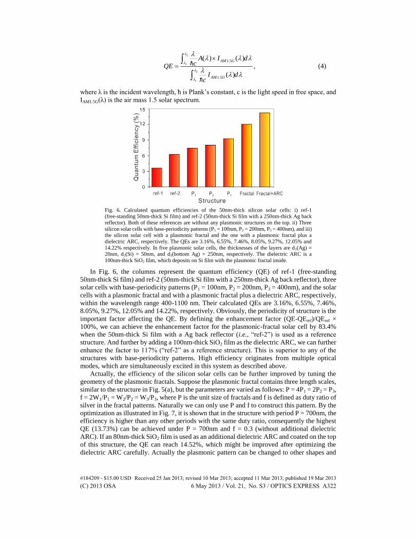
Fig. 6. Calculated quantum efficiencies of the 50nm-thick silicon solar cells: i) ref-1 (free-standing 50nm-thick Si film) and ref-2 (50nm-thick Si film with a 250nm-thick Ag back
reflector). Both of these references are without any plasmonic structures on the top. ii) Three
silicon solar cells with base-periodicity patterns (P1 = 100nm, P2 = 200nm, P3 = 400nm), and iii) the silicon solar cell with a plasmonic fractal and the one with a plasmonic fractal plus a
dielectric ARC, respectively. The QEs are 3.16%, 6.55%, 7.46%, 8.05%, 9.27%, 12.05% and
14.22% respectively. In five plasmonic solar cells, the thicknesses of the layers are d1(Ag) = 20nm, d2(Si) = 50nm, and d3(bottom Ag) = 250nm, respectively. The dielectric ARC is a
100nm-thick SiO2 film, which deposits on Si film with the plasmonic fractal inside.
In Fig. 6, the columns represent the quantum efficiency (QE) of ref-1 (free-standing
50nm-thick Si film) and ref-2 (50nm-thick Si film with a 250nm-thick Ag back reflector), three
solar cells with base-periodicity patterns (P1 = 100nm, P2 = 200nm, P3 = 400nm), and the solar
cells with a plasmonic fractal and with a plasmonic fractal plus a dielectric ARC, respectively,
within the wavelength range 400-1100 nm. Their calculated QEs are 3.16%, 6.55%, 7.46%,
8.05%, 9.27%, 12.05% and 14.22%, respectively. Obviously, the periodicity of structure is the
important factor affecting the QE. By defining the enhancement factor (QE-QEref)/QEref ×
100%, we can achieve the enhancement factor for the plasmonic-fractal solar cell by 83.4%
when the 50nm-thick Si film with a Ag back reflector (i.e., “ref-2”) is used as a reference
structure. And further by adding a 100nm-thick SiO2 film as the dielectric ARC, we can further
enhance the factor to 117% (“ref-2” as a reference structure). This is superior to any of the
structures with base-periodicity patterns. High efficiency originates from multiple optical
modes, which are simultaneously excited in this system as described above.
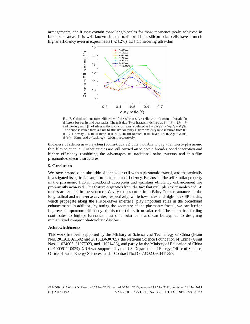
Actually, the efficiency of the silicon solar cells can be further improved by tuning the
geometry of the plasmonic fractals. Suppose the plasmonic fractal contains three length scales,
similar to the structure in Fig. 5(a), but the parameters are varied as follows: P = 4P1 = 2P2 = P3,
f = 2W1/P1 = W2/P2 = W3/P3, where P is the unit size of fractals and f is defined as duty ratio of
silver in the fractal patterns. Naturally we can only use P and f to construct this pattern. By the
optimization as illustrated in Fig. 7, it is shown that in the structure with period P = 700nm, the
efficiency is higher than any other periods with the same duty ratio, consequently the highest
QE (13.73%) can be achieved under P = 700nm and f = 0.3 (without additional dielectric
ARC). If an 80nm-thick SiO2 film is used as an additional dielectric ARC and coated on the top
of this structure, the QE can reach 14.52%, which might be improved after optimizing the
dielectric ARC carefully. Actually the plasmonic pattern can be changed to other shapes and
#184209 - $15.00 USD Received 25 Jan 2013; revised 10 Mar 2013; accepted 11 Mar 2013; published 19 Mar 2013(C) 2013 OSA 6 May 2013 / Vol. 21, No. S3 / OPTICS EXPRESS A322
arrangements, and it may contain more length-scales for more resonance peaks achieved in
broadband areas. It is well known that the traditional bulk silicon solar cells have a much
higher efficiency even in experiments (~24.2%) [33]. Considering ultra-thin
Fig. 7. Calculated quantum efficiency of the silicon solar cells with plasmonic fractals for
different base-units and duty ratios. The unit size (P) of fractals is defined as P = 4P1 = 2P2 = P3
and the duty ratio (f) of silver in the fractal patterns is defined as f = 2W1/P1 = W2/P2 = W3/P3. The period is varied from 400nm to 1000nm for every 100nm and duty ratio is varied from 0.3
to 0.7 for every 0.1. In all these solar cells, the thicknesses of the layers are d1(Ag) = 20nm,
d2(Si) = 50nm, and d3(back Ag) = 250nm, respectively.
thickness of silicon in our system (50nm-thick Si), it is valuable to pay attention to plasmonic
thin-film solar cells. Further studies are still carried on to obtain broader-band absorption and
higher efficiency combining the advantages of traditional solar systems and thin-film
plasmonic/dielectric structures.
5. Conclusion
We have proposed an ultra-thin silicon solar cell with a plasmonic fractal, and theoretically
investigated its optical absorption and quantum efficiency. Because of the self-similar property
in the plasmonic fractal, broadband absorption and quantum efficiency enhancement are
prominently achieved. This feature originates from the fact that multiple cavity modes and SP
modes are excited in the structure. Cavity modes come from Fabry-Perot resonances at the
longitudinal and transverse cavities, respectively; while low-index and high-index SP modes,
which propagate along the silicon-silver interface, play important roles in the broadband
enhancement. In addition, by tuning the geometry of the plasmonic fractal, we can further
improve the quantum efficiency of this ultra-thin silicon solar cell. The theoretical finding
contributes to high-performance plasmonic solar cells and can be applied to designing
miniaturized compact photovoltaic devices.
Acknowledgments
This work has been supported by the Ministry of Science and Technology of China (Grant
Nos. 2012CB921502 and 2010CB630705), the National Science Foundation of China (Grant
Nos. 11034005, 61077023, and 11021403), and partly by the Ministry of Education of China
(20100091110029). XRH was supported by the U.S. Department of Energy, Office of Science,
Office of Basic Energy Sciences, under Contract No.DE-AC02-06CH11357.
#184209 - $15.00 USD Received 25 Jan 2013; revised 10 Mar 2013; accepted 11 Mar 2013; published 19 Mar 2013(C) 2013 OSA 6 May 2013 / Vol. 21, No. S3 / OPTICS EXPRESS A323