Embed Size (px)
Citation preview
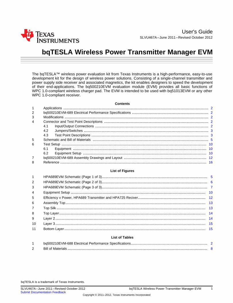
User's GuideSLVU467A–June 2011–Revised October 2012
bqTESLA Wireless Power Transmitter Manager EVM
The bqTESLA™ wireless power evaluation kit from Texas Instruments is a high-performance, easy-to-usedevelopment kit for the design of wireless power solutions. Consisting of a single-channel transmitter andpower supply side receiver and associated magnetics, the kit enables designers to speed the developmentof their end-applications. The bq500210EVM evaluation module (EVM) provides all basic functions ofWPC 1.0-compliant wireless charger pad. The EVM is intended to be used with bq51013EVM or any otherWPC 1.0-compliant receiver.
Contents1 Applications .................................................................................................................. 22 bq500210EVM-689 Electrical Performance Specifications ............................................................ 23 Modifications ................................................................................................................. 24 Connector and Test Point Descriptions .................................................................................. 2
4.1 Input/Output Connections ......................................................................................... 24.2 Jumpers/Switches .................................................................................................. 34.3 Test Point Descriptions ............................................................................................ 3
5 Schematic and Bill of Materials ........................................................................................... 56 Test Setup .................................................................................................................. 10
6.1 Equipment ......................................................................................................... 106.2 Equipment Setup ................................................................................................. 10
7 bq500210EVM-689 Assembly Drawings and Layout ................................................................. 128 Reference ................................................................................................................... 16
List of Figures
1 HPA689EVM Schematic (Page 1 of 3)................................................................................... 5
2 HPA689EVM Schematic (Page 2 of 3)................................................................................... 6
3 HPA689EVM Schematic (Page 3 of 3)................................................................................... 7
4 Equipment Setup .......................................................................................................... 10
5 Efficiency v Power, HPA689 Transmitter and HPA725 Reciver..................................................... 12
6 Assembly Top .............................................................................................................. 13
7 Top Silk ..................................................................................................................... 13
8 Top Layer................................................................................................................... 14
9 Layer 2 ...................................................................................................................... 14
10 Layer 3 ...................................................................................................................... 15
11 Bottom Layer ............................................................................................................... 15
List of Tables
1 bq500210EVM-688 Electrical Performance Specifications............................................................ 2
2 Bill of Materials .............................................................................................................. 8
bqTESLA is a trademark of Texas Instruments.
1SLVU467A–June 2011–Revised October 2012 bqTESLA Wireless Power Transmitter Manager EVMSubmit Documentation Feedback
Copyright © 2011–2012, Texas Instruments Incorporated
Applications www.ti.com
1 Applications
The bq500210EVM-689 evaluation module demonstrates the transmitter portion of the bqTESLA™wireless power system. This transmitter EVM is a complete transmitter-side solution that powers abqTESLA™ receiver. The bq500210EVM requires single 19-V at 0.5 A power supply to operate andcombines on the single printed-circuit board the transmitter electronics, input power socket, LEDindicators, and the transmitting coil. The open design allows easy access to key points of the electricalschematic. The board has installed connectors for optional JTAG and serial interfaces that can be helpfulto advanced users. This EVM has the following features.
• WPC-certified transmitter
• Transmitter mounting pad to provide correct receiver interface
• Receiver output voltage of 5 V up to 1 A
• Standard A1-type transmitter coil
• LED indicates power transfer state and buzzer indicates start of power transfer.
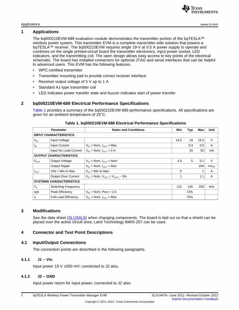
2 bq500210EVM-689 Electrical Performance Specifications
Table 1 provides a summary of the bq500210EVM-689 performance specifications. All specifications aregiven for an ambient temperature of 25°C.
Table 1. bq500210EVM-688 Electrical Performance Specifications
Parameter Notes and Conditions Min Typ Max Unit
INPUT CHARACTERISTICS
VIN Input Voltage 18.5 19 19.5 V
IIN Input Current VIN = Nom, IOUT = Max 0.3 0.5 A
Input No Load Current VIN = Nom, IOUT = 0 A 20 50 mA
OUTPUT CHARACTERISTICS
VOUT Output Voltage VIN = Nom, IOUT = Nom 4.5 5 5.1 V
Output Ripple VIN = Nom, IOUT = Max 200 mVPP
IOUT VIN = Min to Max VIN = Min to Max 0 1 A
Output Over Current VIN = Nom, VOUT = VOUT1 - 5% 1 1.1 A
SYSTEMS CHARACTERISTICS
FS Switching Frequency 110 145 200 kHz
ηpk Peak Efficiency VIN = Nom; Porx = 2.5 72%
η Full-Load Efficiency VIN = Nom, IOUT = Max 70%
3 Modifications
See the data sheet (SLUSAL8) when changing components. The board is laid out so that a shield can beplaced over the active circuit area; Laird Technology BMIS-207 can be used.
4 Connector and Test Point Descriptions
4.1 Input/Output Connections
The connection points are described in the following paragraphs.
4.1.1 J1 – Vin
Input power 19 V ±500 mV; connected to J2 also.
4.1.2 J2 – GND
Input power return for input power; connected to J2 also.
2 bqTESLA Wireless Power Transmitter Manager EVM SLVU467A–June 2011–Revised October 2012Submit Documentation Feedback
Copyright © 2011–2012, Texas Instruments Incorporated
www.ti.com Connector and Test Point Descriptions
4.1.3 J3 – I2C interface
Factory use only
4.1.4 J4 – JTAG (Not Installed)
Factory use only
4.1.5 J5 – Metal Object Detection Threshold
Connection point for external resistor to set trip point for Metal Object Detection. See the bq500210 datasheet for more information (SLUSAL8).
4.1.6 J6 – Select LED Mode
Connection point for external resistor to select LED mode. See the bq500210 data sheet for moreinformation.
4.1.7 J7 – Vin
Input power 19 V ±500 mV; connected to J2 also.
4.1.8 JP1 – NTC
Connection point for external temperature sensor. See the data sheet for more information.
4.2 Jumpers/Switches
The control jumpers are described in the following paragraphs.
4.2.1 R23 – LED Scheme
LED indication scheme set resistor; default 42.2 kΩ. For a detailed function description, see the bq500210data sheet
4.2.2 R51 – MOD-THR
MOD threshold set resistor; default 100 kΩ. For a detailed function description, see the bq500210 datasheet.
4.3 Test Point Descriptions
The test points are described in the following paragraphs.
4.3.1 TP1 – Coil Monitor 1
Test point for measuring ac voltage applied to TX coil.
4.3.2 TP2 – Coil Monitor 2
Test point for measuring ac voltage applied to TX coil.
4.3.3 TP3 – PWR GND
Ground for Switch circuits.
4.3.4 TP4 – Analog GND
Low noise GND
3SLVU467A–June 2011–Revised October 2012 bqTESLA Wireless Power Transmitter Manager EVMSubmit Documentation Feedback
Copyright © 2011–2012, Texas Instruments Incorporated
Connector and Test Point Descriptions www.ti.com
4.3.5 TP5 – Analog GND
Low noise GND
4.3.6 TP6 – Analog GND
Low noise GND
4.3.7 TP7 – Analog GND
Low noise GND
4.3.8 TP8 – DC Buzzer Output
Connection point for external dc buzzer; logic high for 500 ms at start of power transfer to receiver unit.
4.3.9 TP9 – 3.3V Input DC Current
3.3V output from U5 used for low power circuit.
4.3.10 TP10 - Filtered 3.3V
3.3V output with additional filtering for A to D convererters.
4.3.11 TP11 – Gate Drive Voltage
Input voltage to U2, gate driver for power switches.
4.3.12 TP12 – MSP430 3.3V
Filtered 3.3V for MSP430, U4.
4.3.13 TP13 – Demodulation Comm 1 Output
Primary communications channel, input to bq500210 from demodulation circuit.
4.3.14 TP14 – Sleep
Output from bq500210 to 500 ms timer circuit.
4 bqTESLA Wireless Power Transmitter Manager EVM SLVU467A–June 2011–Revised October 2012Submit Documentation Feedback
Copyright © 2011–2012, Texas Instruments Incorporated
R29
R36
R13
Q3
U3
Q1
R33
R32
R3
R34
R6
R5
C21
C23
C9
C29
C14
C13
C15
C27
Q2
R7
U2
R14
R9
C17
C18
D3
C16
TP1 TP2
L2
C7
TP3
R26
TP11
TP13
D4
U5
D1
R1
R4
R37
C2 C31
C6 C25
C30
C32
L1C26
C28
R42
D2
J1
J2
TP4 TP5TP6TP7
5
4
6
12
3
1
23
4 5
6
7 8 12
12
3
4 5
67
8
1
2
1
2
UGATE
BOOTPWM
GND LGATE
VDD
EN/PG PHSE
BOOTVIN
EN
SS VSENS
COMPGND
PH
10
309k
190k
BC847CL
INA214DCK
CSD17308Q3
1.00
1.00
10.0
0
200k
10.0k
0.01uF
0.1uF
0.1uF
0.22uF
33pF
0.047uF
0.047uF
22uF
CSD17308Q3
0.020
TPS28225D
23.2k
1.00k
0.1uF
4700pF
BAT54SW
0.1uF
IND_EC00296A
xx uH
22uF
10
TPS54231D
MBR0540
10.0k
3.16k
76.8k
47uF
10uF 0.1uF
0.1uF
2700pF
330uH
0.1uF
0.01uF
475
LTST-C190GKT
Power Train
19 VinDC in
Buck Regulator
F
DPWM-1A
I_SENSE
COMM+
COMM-
3V3_VCC
VIN
VIN
3V3_VCC
VIN
3V3_VCC
www.ti.com Schematic and Bill of Materials
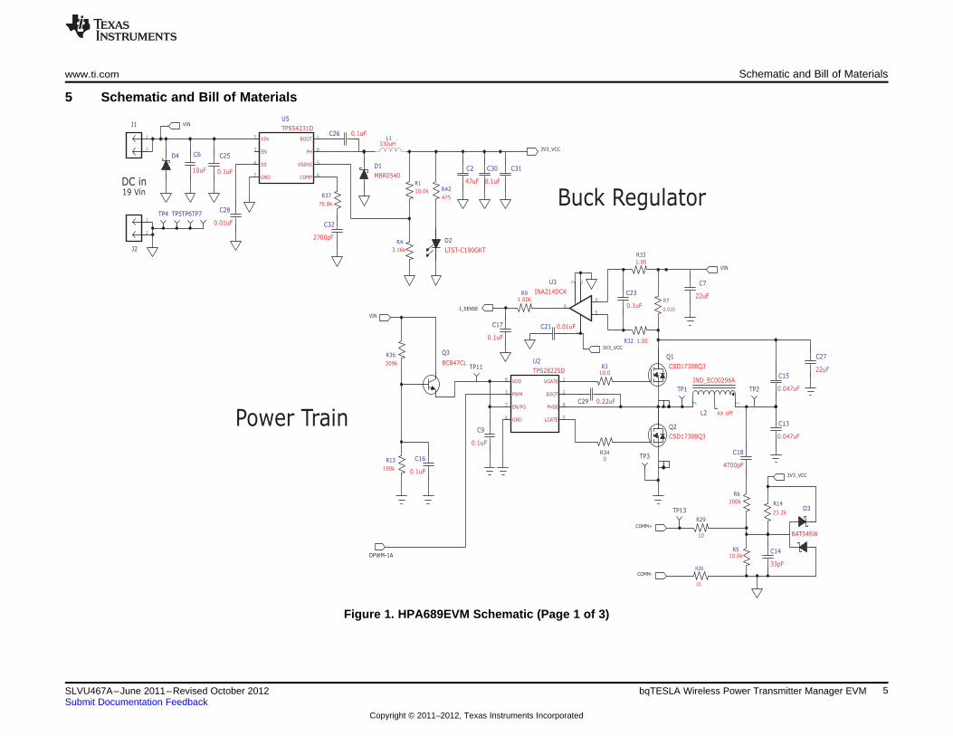
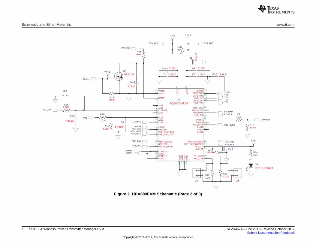
5 Schematic and Bill of Materials
Figure 1. HPA689EVM Schematic (Page 1 of 3)
5SLVU467A–June 2011–Revised October 2012 bqTESLA Wireless Power Transmitter Manager EVMSubmit Documentation Feedback
Copyright © 2011–2012, Texas Instruments Incorporated
R11
R10
BUZ
C1
C4
C19
C3
C5
Q4
R18
C22
R22R23
C20
R25
R19
C24R2
R17
JP1
J5 J6
U1
R44
D6
TP8
TP9TP10
TP14
R45
C8
R30
1
2
1
2
1
2
3
4
5
6
7
8
9
10
11
12
13
14
15
16
17
18
19
20
21
22
23
24
25
26
27
28
29
30
31
32
33
34
35
36
37
38
39
40
41
42
43
44
45
46
47
48
49
12
AIN5
T_SENSE
AIN3
AIN8
RESET
LOBAT
MSP_RST
MSP_TMS/MISO
MSP_JTAG_TEST
PMB_CLK
PMB_DATA
PWM_A
PWM_B
MSP_SYNC
DIO2B
DIO4A
DIO4B
MSP_TCK/CLK
PMB_ALERT
PMB_CTRL
DRV_SEL
BRIDGE_MODE
BUZ_AC
BUZ_DC
MSP_TDI/MOSI/SUP
MSP_TDO/PROG
JTAG_TCK
JTAG_TDO
JTAG_TDI
JATG_TMS
JTAG_TRST
DG
ND
V33D
V33A
BPCAP
AG
ND
COMM_A
AGND
COMM_B
AGND
V33FB
I_IN
MOD_THR
LED_MODE
AIN7
V_IN
AG
N2
AGND
EPAD
2.00k
15.4k
1.0uF
4700pF
4.7uF
1.0uF
4.7uF
BSS138
10.0k
4.7uF
100k42.2k
1.0uF
280k
2.00k
4700pF
10.0
10.0k
BQ500210RGZ
475
LTST-C190GKT
10.0K
0.0
1uF22
VIN
I_SENSE
COMM+
PM_DATA
PM_CLK
MSP_SYNC
SLEEP
SLEEP
MSP_RST
MSP_MISO
MSP_TEST
MSP_CLKMSP_RDY
MSP_MOSI
DPWM-1A
3V3_VCC
/TRST
TMS
TDI
TDO
TCK
COMM-
3V3_VCC
3V3_VCC
3V3_VCC
3V3_ADC
Schematic and Bill of Materials www.ti.com
Figure 2. HPA689EVM Schematic (Page 2 of 3)
6 bqTESLA Wireless Power Transmitter Manager EVM SLVU467A–June 2011–Revised October 2012Submit Documentation Feedback
Copyright © 2011–2012, Texas Instruments Incorporated
SHD1
J4
J3
R20 R21R31R35R38R39 R40R41
R43
R27R28
D5
U4
R15
R8
R12R16
C10
C11
C12
R24
TP12
1
2
3
4
5
6
7
8
9
10
1
2
3
4
5
6
7
8
9
10
11
12
13
14
1
2
3
4
5
6
7 8
9
10
11
12
13
14VCC
P1.0
P1.1
P1.2
P1.3
P1.4
P1.5 P1.6
P1.7
RST
TEST
XOUT
XIN
GND
10.0k 10.0k
475475
HSMF-C165
MSP430G2001
10.0k
10.0k10.0k0.01uF
4.7uF
1.0uF
10.0
Low Power Supervisor
STATUS
I2C and JTAG Connector--Factory Use Only
EMI Shield
PM_DATA
PM_CLK
TMS
/TRST
TDI
TDO
TCK
3V3_VCC
MSP_TEST
MSP_RST
MSP_MISO
MSP_CLK
MSP_MOSI
MSP_RDY
MSP_SYNC
3V3_VCC
www.ti.com Schematic and Bill of Materials
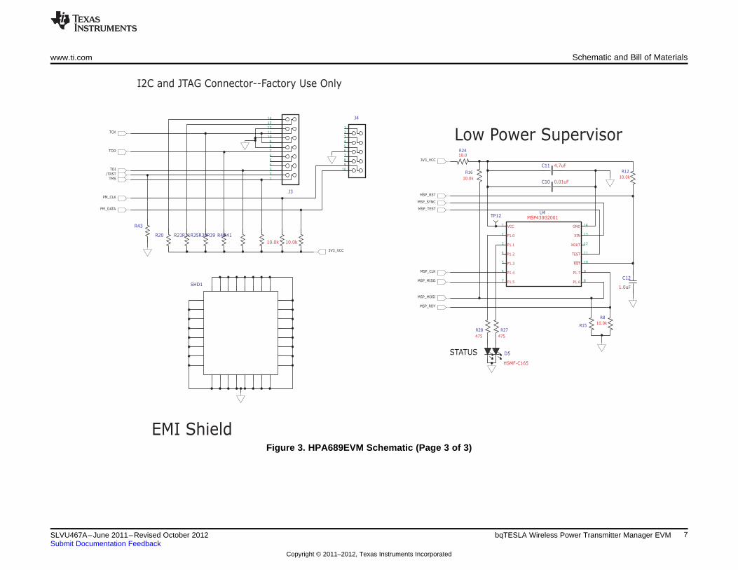
Figure 3. HPA689EVM Schematic (Page 3 of 3)
7SLVU467A–June 2011–Revised October 2012 bqTESLA Wireless Power Transmitter Manager EVMSubmit Documentation Feedback
Copyright © 2011–2012, Texas Instruments Incorporated
Schematic and Bill of Materials www.ti.com
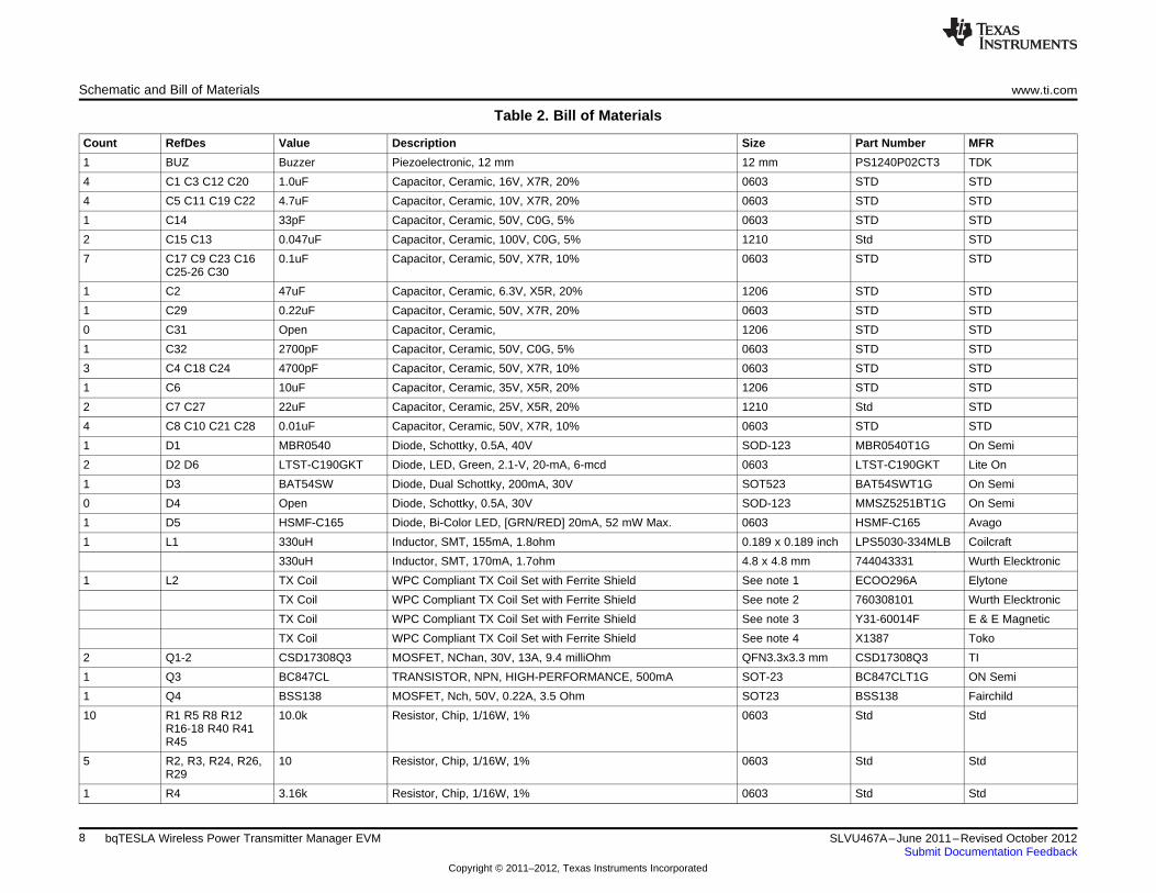
Table 2. Bill of Materials
Count RefDes Value Description Size Part Number MFR
1 BUZ Buzzer Piezoelectronic, 12 mm 12 mm PS1240P02CT3 TDK
4 C1 C3 C12 C20 1.0uF Capacitor, Ceramic, 16V, X7R, 20% 0603 STD STD
4 C5 C11 C19 C22 4.7uF Capacitor, Ceramic, 10V, X7R, 20% 0603 STD STD
1 C14 33pF Capacitor, Ceramic, 50V, C0G, 5% 0603 STD STD
2 C15 C13 0.047uF Capacitor, Ceramic, 100V, C0G, 5% 1210 Std STD
7 C17 C9 C23 C16 0.1uF Capacitor, Ceramic, 50V, X7R, 10% 0603 STD STDC25-26 C30
1 C2 47uF Capacitor, Ceramic, 6.3V, X5R, 20% 1206 STD STD
1 C29 0.22uF Capacitor, Ceramic, 50V, X7R, 20% 0603 STD STD
0 C31 Open Capacitor, Ceramic, 1206 STD STD
1 C32 2700pF Capacitor, Ceramic, 50V, C0G, 5% 0603 STD STD
3 C4 C18 C24 4700pF Capacitor, Ceramic, 50V, X7R, 10% 0603 STD STD
1 C6 10uF Capacitor, Ceramic, 35V, X5R, 20% 1206 STD STD
2 C7 C27 22uF Capacitor, Ceramic, 25V, X5R, 20% 1210 Std STD
4 C8 C10 C21 C28 0.01uF Capacitor, Ceramic, 50V, X7R, 10% 0603 STD STD
1 D1 MBR0540 Diode, Schottky, 0.5A, 40V SOD-123 MBR0540T1G On Semi
2 D2 D6 LTST-C190GKT Diode, LED, Green, 2.1-V, 20-mA, 6-mcd 0603 LTST-C190GKT Lite On
1 D3 BAT54SW Diode, Dual Schottky, 200mA, 30V SOT523 BAT54SWT1G On Semi
0 D4 Open Diode, Schottky, 0.5A, 30V SOD-123 MMSZ5251BT1G On Semi
1 D5 HSMF-C165 Diode, Bi-Color LED, [GRN/RED] 20mA, 52 mW Max. 0603 HSMF-C165 Avago
1 L1 330uH Inductor, SMT, 155mA, 1.8ohm 0.189 x 0.189 inch LPS5030-334MLB Coilcraft
330uH Inductor, SMT, 170mA, 1.7ohm 4.8 x 4.8 mm 744043331 Wurth Elecktronic
1 L2 TX Coil WPC Compliant TX Coil Set with Ferrite Shield See note 1 ECOO296A Elytone
TX Coil WPC Compliant TX Coil Set with Ferrite Shield See note 2 760308101 Wurth Elecktronic
TX Coil WPC Compliant TX Coil Set with Ferrite Shield See note 3 Y31-60014F E & E Magnetic
TX Coil WPC Compliant TX Coil Set with Ferrite Shield See note 4 X1387 Toko
2 Q1-2 CSD17308Q3 MOSFET, NChan, 30V, 13A, 9.4 milliOhm QFN3.3x3.3 mm CSD17308Q3 TI
1 Q3 BC847CL TRANSISTOR, NPN, HIGH-PERFORMANCE, 500mA SOT-23 BC847CLT1G ON Semi
1 Q4 BSS138 MOSFET, Nch, 50V, 0.22A, 3.5 Ohm SOT23 BSS138 Fairchild
10 R1 R5 R8 R12 10.0k Resistor, Chip, 1/16W, 1% 0603 Std StdR16-18 R40 R41R45
5 R2, R3, R24, R26, 10 Resistor, Chip, 1/16W, 1% 0603 Std StdR29
1 R4 3.16k Resistor, Chip, 1/16W, 1% 0603 Std Std
8 bqTESLA Wireless Power Transmitter Manager EVM SLVU467A–June 2011–Revised October 2012Submit Documentation Feedback
Copyright © 2011–2012, Texas Instruments Incorporated
www.ti.com Schematic and Bill of Materials
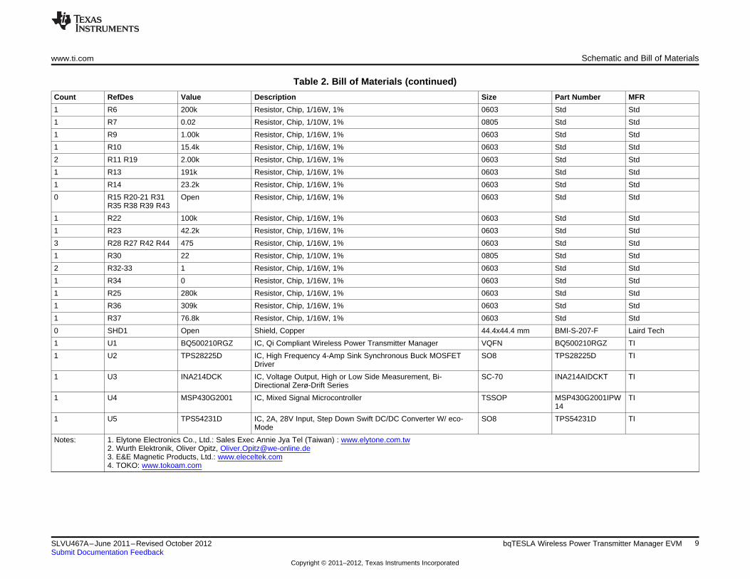
Table 2. Bill of Materials (continued)
Count RefDes Value Description Size Part Number MFR
1 R6 200k Resistor, Chip, 1/16W, 1% 0603 Std Std
1 R7 0.02 Resistor, Chip, 1/10W, 1% 0805 Std Std
1 R9 1.00k Resistor, Chip, 1/16W, 1% 0603 Std Std
1 R10 15.4k Resistor, Chip, 1/16W, 1% 0603 Std Std
2 R11 R19 2.00k Resistor, Chip, 1/16W, 1% 0603 Std Std
1 R13 191k Resistor, Chip, 1/16W, 1% 0603 Std Std
1 R14 23.2k Resistor, Chip, 1/16W, 1% 0603 Std Std
0 R15 R20-21 R31 Open Resistor, Chip, 1/16W, 1% 0603 Std StdR35 R38 R39 R43
1 R22 100k Resistor, Chip, 1/16W, 1% 0603 Std Std
1 R23 42.2k Resistor, Chip, 1/16W, 1% 0603 Std Std
3 R28 R27 R42 R44 475 Resistor, Chip, 1/16W, 1% 0603 Std Std
1 R30 22 Resistor, Chip, 1/10W, 1% 0805 Std Std
2 R32-33 1 Resistor, Chip, 1/16W, 1% 0603 Std Std
1 R34 0 Resistor, Chip, 1/16W, 1% 0603 Std Std
1 R25 280k Resistor, Chip, 1/16W, 1% 0603 Std Std
1 R36 309k Resistor, Chip, 1/16W, 1% 0603 Std Std
1 R37 76.8k Resistor, Chip, 1/16W, 1% 0603 Std Std
0 SHD1 Open Shield, Copper 44.4x44.4 mm BMI-S-207-F Laird Tech
1 U1 BQ500210RGZ IC, Qi Compliant Wireless Power Transmitter Manager VQFN BQ500210RGZ TI
1 U2 TPS28225D IC, High Frequency 4-Amp Sink Synchronous Buck MOSFET SO8 TPS28225D TIDriver
1 U3 INA214DCK IC, Voltage Output, High or Low Side Measurement, Bi- SC-70 INA214AIDCKT TIDirectional Zerø-Drift Series
1 U4 MSP430G2001 IC, Mixed Signal Microcontroller TSSOP MSP430G2001IPW TI14
1 U5 TPS54231D IC, 2A, 28V Input, Step Down Swift DC/DC Converter W/ eco- SO8 TPS54231D TIMode
Notes: 1. Elytone Electronics Co., Ltd.: Sales Exec Annie Jya Tel (Taiwan) : www.elytone.com.tw2. Wurth Elektronik, Oliver Opitz, [email protected]. E&E Magnetic Products, Ltd.: www.eleceltek.com4. TOKO: www.tokoam.com
9SLVU467A–June 2011–Revised October 2012 bqTESLA Wireless Power Transmitter Manager EVMSubmit Documentation Feedback
Copyright © 2011–2012, Texas Instruments Incorporated
+
- V
Wireless Transmitter
Bq500210EVM-689
V
A
A
RL
LP LS
AC1
OUT-J2
VIN
VRECT-TP12
AC2
GND-J4
OUT-TP7
Wireless Receiver
bq51013EVM-725
J1
POS
J2
RTN
TP1
AC1
TP2
AC2
Test Setup www.ti.com
6 Test Setup
6.1 Equipment
6.1.1 bqTESLA™ Receiver
Use bq51013EVM-725 (BQ51013EVM) or WPC Gen 1.0-compliant receiver to work with this EVM.
6.1.2 Voltage Source
Input voltage source must provide regulated dc voltage of 19 V and be able to deliver at least 0.5-Acontinuous load current, current limit should be set to 1A.
6.1.3 Meters
Output voltage can be monitor at bq51013EVM-725 TP7 with a voltmeter. Input current into the load mustbe monitored with an appropriate ammeter. Transmitter input current and voltage can be monitored also,but the meter must use averaging function for reducing error due to communications packets.
6.1.4 Loads
A single load is required for 5 V with a maximum current of 1 A. The load can be resistive or electronic.
6.1.5 Oscilloscope
A dual-channel oscilloscope with appropriate probes is used to observe the COMM_DRV signal atbq51013EVM-725 TP3 and other signals. .
6.1.6 Recommended Wire Gauge
For proper operation, 22 AWG wire is recommended when connecting the bq500210EVM-689 to inputsupply and bq51013EVM-725 to load.
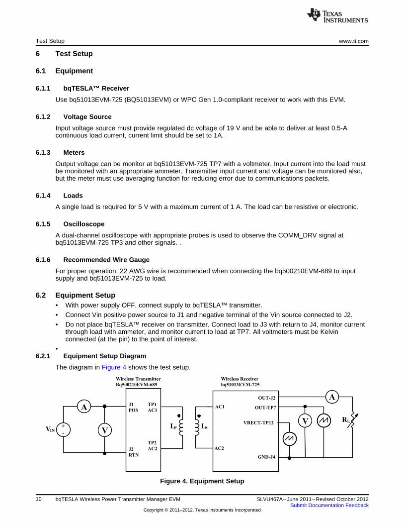
6.2 Equipment Setup• With power supply OFF, connect supply to bqTESLA™ transmitter.
• Connect Vin positive power source to J1 and negative terminal of the Vin source connected to J2.
• Do not place bqTESLA™ receiver on transmitter. Connect load to J3 with return to J4, monitor currentthrough load with ammeter, and monitor current to load at TP7. All voltmeters must be Kelvinconnected (at the pin) to the point of interest.
•6.2.1 Equipment Setup Diagram
The diagram in Figure 4 shows the test setup.
Figure 4. Equipment Setup
10 bqTESLA Wireless Power Transmitter Manager EVM SLVU467A–June 2011–Revised October 2012Submit Documentation Feedback
Copyright © 2011–2012, Texas Instruments Incorporated
www.ti.com Test Setup
6.2.2 EVM Procedures
This section guides the user through a few general test procedures to exercise the functionality of thepresented hardware. Some key notes follow:
6.2.2.1 START UP NO RX
Turn on VIN, and observe that the Green Power LED D2 illuminates. Status LED D5 will be off until powertranfer starts.
Apply the scope probe to the test point TP1 and observe a single pulse bursts approximately every 0.5 s.This is Analog Ping probing environment for the presence of a receiver placed on the Tx coil.
6.2.2.2 APPLY RX
Place bq51013EVM-725 EVM on the top of the transmitting coil. Align centers of the receiving andtransmitting coils across each other. In the next few seconds, observe Status LED D5 illuminates green,indicating that communication between transmitter and receiver is established and power transfer hasbegan.
• Buzzer will sound at the start of power transfer. Status LED D5 flashes green light during powertransfer.
• Typical output voltage is 5 V, and the output current range is 0 mA to 1A.
• Observe continuous sine-wave on the test point TP1 when power transfer is active, frequency will bebetween 110kHz and 205kHz.
• Make tests and measurements applicable to a normal 5V power supply.
6.2.2.3 EFFICIENCY
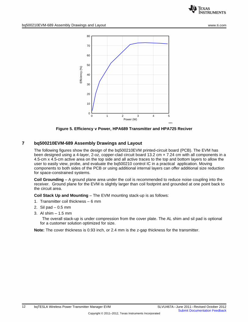
To measure system efficiency, measure the output voltage, the output current, input voltage, and inputcurrent and calculate efficiency as the ratio of the output power to the input power. It is recommended toaverage the input current, the comm pulses will modulate the input current distorting the reading. SeeFigure 5 for efficiency.
6.2.2.4 PARASITIC METAL OBJECT DETECTION
To test the Metal Object Detection (MOD) function. In addition to loading on the output of bq51013EVM-725, apply an electronic load in constant power mode between secondary GND (J4) and TP12 – theoutput of the secondary side rectifier. Increasing load power from 0 W to over 0.5 W, observe LED D5 ofbq500210EVM turning red and the power transfer stopped in approximately 20 s after the MOD thresholdwas exceeded.
6.2.2.5 THERMAL PROTECTION, NTC
Thermal protection is provided by an NTC resistor connected to JP1. At 1.00V on the sense side (U1-2)thermal fault will be set and unit is shutdown, Status LED D5 will illuminate red. Typical resistor value forfault is 850 ohms. System will try to restart in 5 minutes.
11SLVU467A–June 2011–Revised October 2012 bqTESLA Wireless Power Transmitter Manager EVMSubmit Documentation Feedback
Copyright © 2011–2012, Texas Instruments Incorporated
0
10
20
30
40
50
60
70
80
0 1 2 3 4 5Power (W)
Effi
cien
cy (
%)
G001
bq500210EVM-689 Assembly Drawings and Layout www.ti.com
Figure 5. Efficiency v Power, HPA689 Transmitter and HPA725 Reciver
7 bq500210EVM-689 Assembly Drawings and Layout
The following figures show the design of the bq500210EVM printed-circuit board (PCB). The EVM hasbeen designed using a 4-layer, 2-oz, copper-clad circuit board 13.2 cm × 7.24 cm with all components in a4.5-cm x 4.5-cm active area on the top side and all active traces to the top and bottom layers to allow theuser to easily view, probe, and evaluate the bq500210 control IC in a practical application. Movingcomponents to both sides of the PCB or using additional internal layers can offer additional size reductionfor space-constrained systems.
Coil Grounding – A ground plane area under the coil is recommended to reduce noise coupling into thereceiver. Ground plane for the EVM is slightly larger than coil footprint and grounded at one point back tothe circuit area.
Coil Stack Up and Mounting – The EVM mounting stack-up is as follows:
1. Transmitter coil thickness – 6 mm
2. Sil pad – 0.5 mm
3. Al shim – 1.5 mmThe overall stack-up is under compression from the cover plate. The AL shim and sil pad is optional
for a customer solution optimized for size.
Note: The cover thickness is 0.93 inch, or 2.4 mm is the z-gap thickness for the transmitter.
12 bqTESLA Wireless Power Transmitter Manager EVM SLVU467A–June 2011–Revised October 2012Submit Documentation Feedback
Copyright © 2011–2012, Texas Instruments Incorporated
www.ti.com bq500210EVM-689 Assembly Drawings and Layout
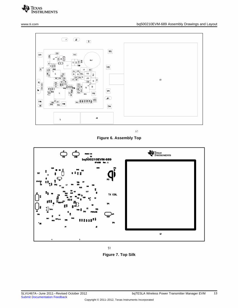
Figure 6. Assembly Top
Figure 7. Top Silk
13SLVU467A–June 2011–Revised October 2012 bqTESLA Wireless Power Transmitter Manager EVMSubmit Documentation Feedback
Copyright © 2011–2012, Texas Instruments Incorporated
bq500210EVM-689 Assembly Drawings and Layout www.ti.com
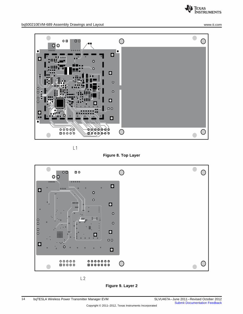
Figure 8. Top Layer
Figure 9. Layer 2
14 bqTESLA Wireless Power Transmitter Manager EVM SLVU467A–June 2011–Revised October 2012Submit Documentation Feedback
Copyright © 2011–2012, Texas Instruments Incorporated
www.ti.com bq500210EVM-689 Assembly Drawings and Layout
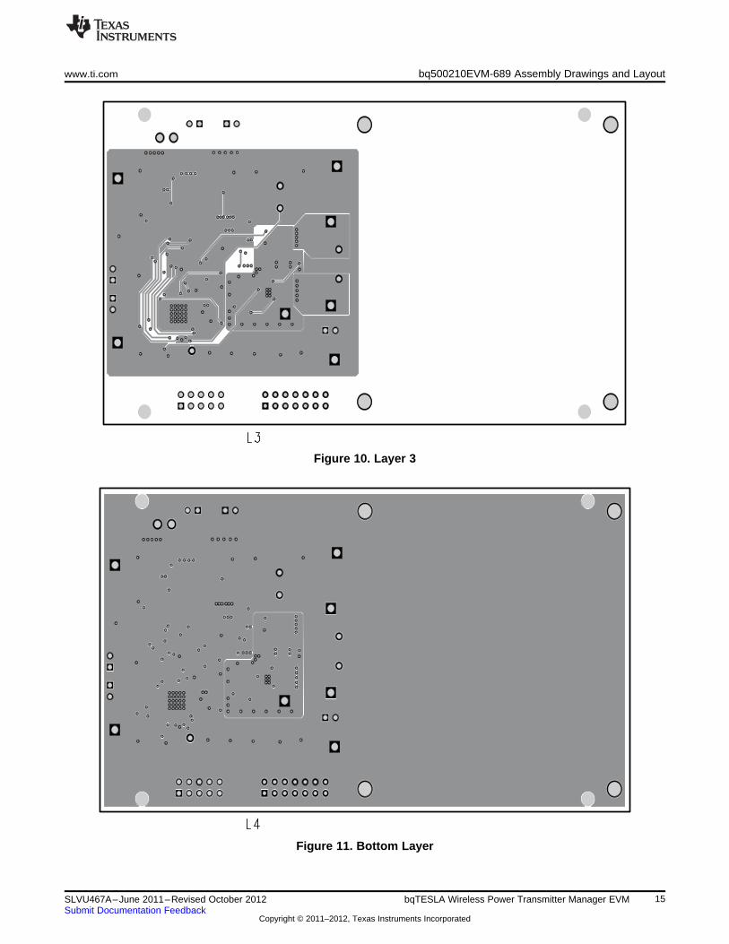
Figure 10. Layer 3
Figure 11. Bottom Layer
15SLVU467A–June 2011–Revised October 2012 bqTESLA Wireless Power Transmitter Manager EVMSubmit Documentation Feedback
Copyright © 2011–2012, Texas Instruments Incorporated
Reference www.ti.com
8 Reference
For additional information about the bq500210EVM-689 low power wireless power evaluation kit fromTexas Instruments, visit the product folder on the TI Web site athttp://focus.ti.com/docs/toolsw/folders/print/bqtesla100lp.html.
16 bqTESLA Wireless Power Transmitter Manager EVM SLVU467A–June 2011–Revised October 2012Submit Documentation Feedback
Copyright © 2011–2012, Texas Instruments Incorporated

EVALUATION BOARD/KIT/MODULE (EVM) ADDITIONAL TERMS
Texas Instruments (TI) provides the enclosed Evaluation Board/Kit/Module (EVM) under the following conditions:
The user assumes all responsibility and liability for proper and safe handling of the goods. Further, the user indemnifies TI from all claimsarising from the handling or use of the goods.
Should this evaluation board/kit not meet the specifications indicated in the User’s Guide, the board/kit may be returned within 30 days fromthe date of delivery for a full refund. THE FOREGOING LIMITED WARRANTY IS THE EXCLUSIVE WARRANTY MADE BY SELLER TOBUYER AND IS IN LIEU OF ALL OTHER WARRANTIES, EXPRESSED, IMPLIED, OR STATUTORY, INCLUDING ANY WARRANTY OFMERCHANTABILITY OR FITNESS FOR ANY PARTICULAR PURPOSE. EXCEPT TO THE EXTENT OF THE INDEMNITY SET FORTHABOVE, NEITHER PARTY SHALL BE LIABLE TO THE OTHER FOR ANY INDIRECT, SPECIAL, INCIDENTAL, OR CONSEQUENTIALDAMAGES.
Please read the User's Guide and, specifically, the Warnings and Restrictions notice in the User's Guide prior to handling the product. Thisnotice contains important safety information about temperatures and voltages. For additional information on TI's environmental and/or safetyprograms, please visit www.ti.com/esh or contact TI.
No license is granted under any patent right or other intellectual property right of TI covering or relating to any machine, process, orcombination in which such TI products or services might be or are used. TI currently deals with a variety of customers for products, andtherefore our arrangement with the user is not exclusive. TI assumes no liability for applications assistance, customer product design,software performance, or infringement of patents or services described herein.
REGULATORY COMPLIANCE INFORMATION
As noted in the EVM User’s Guide and/or EVM itself, this EVM and/or accompanying hardware may or may not be subject to the FederalCommunications Commission (FCC) and Industry Canada (IC) rules.
For EVMs not subject to the above rules, this evaluation board/kit/module is intended for use for ENGINEERING DEVELOPMENT,DEMONSTRATION OR EVALUATION PURPOSES ONLY and is not considered by TI to be a finished end product fit for general consumeruse. It generates, uses, and can radiate radio frequency energy and has not been tested for compliance with the limits of computingdevices pursuant to part 15 of FCC or ICES-003 rules, which are designed to provide reasonable protection against radio frequencyinterference. Operation of the equipment may cause interference with radio communications, in which case the user at his own expense willbe required to take whatever measures may be required to correct this interference.
General Statement for EVMs including a radio
User Power/Frequency Use Obligations: This radio is intended for development/professional use only in legally allocated frequency andpower limits. Any use of radio frequencies and/or power availability of this EVM and its development application(s) must comply with locallaws governing radio spectrum allocation and power limits for this evaluation module. It is the user’s sole responsibility to only operate thisradio in legally acceptable frequency space and within legally mandated power limitations. Any exceptions to this are strictly prohibited andunauthorized by Texas Instruments unless user has obtained appropriate experimental/development licenses from local regulatoryauthorities, which is responsibility of user including its acceptable authorization.
For EVMs annotated as FCC – FEDERAL COMMUNICATIONS COMMISSION Part 15 Compliant
Caution
This device complies with part 15 of the FCC Rules. Operation is subject to the following two conditions: (1) This device may not causeharmful interference, and (2) this device must accept any interference received, including interference that may cause undesired operation.
Changes or modifications not expressly approved by the party responsible for compliance could void the user's authority to operate theequipment.
FCC Interference Statement for Class A EVM devices
This equipment has been tested and found to comply with the limits for a Class A digital device, pursuant to part 15 of the FCC Rules.These limits are designed to provide reasonable protection against harmful interference when the equipment is operated in a commercialenvironment. This equipment generates, uses, and can radiate radio frequency energy and, if not installed and used in accordance with theinstruction manual, may cause harmful interference to radio communications. Operation of this equipment in a residential area is likely tocause harmful interference in which case the user will be required to correct the interference at his own expense.
FCC Interference Statement for Class B EVM devices
This equipment has been tested and found to comply with the limits for a Class B digital device, pursuant to part 15 of the FCC Rules.These limits are designed to provide reasonable protection against harmful interference in a residential installation. This equipmentgenerates, uses and can radiate radio frequency energy and, if not installed and used in accordance with the instructions, may causeharmful interference to radio communications. However, there is no guarantee that interference will not occur in a particular installation. Ifthis equipment does cause harmful interference to radio or television reception, which can be determined by turning the equipment off andon, the user is encouraged to try to correct the interference by one or more of the following measures:
• Reorient or relocate the receiving antenna.• Increase the separation between the equipment and receiver.• Connect the equipment into an outlet on a circuit different from that to which the receiver is connected.• Consult the dealer or an experienced radio/TV technician for help.
For EVMs annotated as IC – INDUSTRY CANADA Compliant
This Class A or B digital apparatus complies with Canadian ICES-003.
Changes or modifications not expressly approved by the party responsible for compliance could void the user’s authority to operate theequipment.
Concerning EVMs including radio transmitters
This device complies with Industry Canada licence-exempt RSS standard(s). Operation is subject to the following two conditions: (1) thisdevice may not cause interference, and (2) this device must accept any interference, including interference that may cause undesiredoperation of the device.
Concerning EVMs including detachable antennas
Under Industry Canada regulations, this radio transmitter may only operate using an antenna of a type and maximum (or lesser) gainapproved for the transmitter by Industry Canada. To reduce potential radio interference to other users, the antenna type and its gain shouldbe so chosen that the equivalent isotropically radiated power (e.i.r.p.) is not more than that necessary for successful communication.
This radio transmitter has been approved by Industry Canada to operate with the antenna types listed in the user guide with the maximumpermissible gain and required antenna impedance for each antenna type indicated. Antenna types not included in this list, having a gaingreater than the maximum gain indicated for that type, are strictly prohibited for use with this device.
Cet appareil numérique de la classe A ou B est conforme à la norme NMB-003 du Canada.
Les changements ou les modifications pas expressément approuvés par la partie responsable de la conformité ont pu vider l’autorité del'utilisateur pour actionner l'équipement.
Concernant les EVMs avec appareils radio
Le présent appareil est conforme aux CNR d'Industrie Canada applicables aux appareils radio exempts de licence. L'exploitation estautorisée aux deux conditions suivantes : (1) l'appareil ne doit pas produire de brouillage, et (2) l'utilisateur de l'appareil doit accepter toutbrouillage radioélectrique subi, même si le brouillage est susceptible d'en compromettre le fonctionnement.
Concernant les EVMs avec antennes détachables
Conformément à la réglementation d'Industrie Canada, le présent émetteur radio peut fonctionner avec une antenne d'un type et d'un gainmaximal (ou inférieur) approuvé pour l'émetteur par Industrie Canada. Dans le but de réduire les risques de brouillage radioélectrique àl'intention des autres utilisateurs, il faut choisir le type d'antenne et son gain de sorte que la puissance isotrope rayonnée équivalente(p.i.r.e.) ne dépasse pas l'intensité nécessaire à l'établissement d'une communication satisfaisante.
Le présent émetteur radio a été approuvé par Industrie Canada pour fonctionner avec les types d'antenne énumérés dans le manueld’usage et ayant un gain admissible maximal et l'impédance requise pour chaque type d'antenne. Les types d'antenne non inclus danscette liste, ou dont le gain est supérieur au gain maximal indiqué, sont strictement interdits pour l'exploitation de l'émetteur.
SPACER
SPACER
SPACER
SPACER
SPACER
SPACER
SPACER
SPACER
【【Important Notice for Users of this Product in Japan】】This development kit is NOT certified as Confirming to Technical Regulations of Radio Law of Japan
If you use this product in Japan, you are required by Radio Law of Japan to follow the instructions below with respect to this product:
1. Use this product in a shielded room or any other test facility as defined in the notification #173 issued by Ministry of Internal Affairs andCommunications on March 28, 2006, based on Sub-section 1.1 of Article 6 of the Ministry’s Rule for Enforcement of Radio Law ofJapan,
2. Use this product only after you obtained the license of Test Radio Station as provided in Radio Law of Japan with respect to thisproduct, or
3. Use of this product only after you obtained the Technical Regulations Conformity Certification as provided in Radio Law of Japan withrespect to this product. Also, please do not transfer this product, unless you give the same notice above to the transferee. Please notethat if you could not follow the instructions above, you will be subject to penalties of Radio Law of Japan.
Texas Instruments Japan Limited(address) 24-1, Nishi-Shinjuku 6 chome, Shinjuku-ku, Tokyo, Japan
http://www.tij.co.jp
【ご使用にあたっての注】
本開発キットは技術基準適合証明を受けておりません。
本製品のご使用に際しては、電波法遵守のため、以下のいずれかの措置を取っていただく必要がありますのでご注意ください。1. 電波法施行規則第6条第1項第1号に基づく平成18年3月28日総務省告示第173号で定められた電波暗室等の試験設備でご使用いただく。2. 実験局の免許を取得後ご使用いただく。3. 技術基準適合証明を取得後ご使用いただく。
なお、本製品は、上記の「ご使用にあたっての注意」を譲渡先、移転先に通知しない限り、譲渡、移転できないものとします。
上記を遵守頂けない場合は、電波法の罰則が適用される可能性があることをご留意ください。
日本テキサス・インスツルメンツ株式会社東京都新宿区西新宿6丁目24番1号西新宿三井ビルhttp://www.tij.co.jp
SPACER
SPACER
SPACER
SPACER
SPACER
SPACER
SPACER
SPACER
SPACER
SPACER
SPACER
SPACER
SPACER
SPACER
SPACER
SPACER
EVALUATION BOARD/KIT/MODULE (EVM)WARNINGS, RESTRICTIONS AND DISCLAIMERS
For Feasibility Evaluation Only, in Laboratory/Development Environments. Unless otherwise indicated, this EVM is not a finishedelectrical equipment and not intended for consumer use. It is intended solely for use for preliminary feasibility evaluation inlaboratory/development environments by technically qualified electronics experts who are familiar with the dangers and application risksassociated with handling electrical mechanical components, systems and subsystems. It should not be used as all or part of a finished endproduct.
Your Sole Responsibility and Risk. You acknowledge, represent and agree that:
1. You have unique knowledge concerning Federal, State and local regulatory requirements (including but not limited to Food and DrugAdministration regulations, if applicable) which relate to your products and which relate to your use (and/or that of your employees,affiliates, contractors or designees) of the EVM for evaluation, testing and other purposes.
2. You have full and exclusive responsibility to assure the safety and compliance of your products with all such laws and other applicableregulatory requirements, and also to assure the safety of any activities to be conducted by you and/or your employees, affiliates,contractors or designees, using the EVM. Further, you are responsible to assure that any interfaces (electronic and/or mechanical)between the EVM and any human body are designed with suitable isolation and means to safely limit accessible leakage currents tominimize the risk of electrical shock hazard.
3. You will employ reasonable safeguards to ensure that your use of the EVM will not result in any property damage, injury or death, evenif the EVM should fail to perform as described or expected.
4. You will take care of proper disposal and recycling of the EVM’s electronic components and packing materials.
Certain Instructions. It is important to operate this EVM within TI’s recommended specifications and environmental considerations per theuser guidelines. Exceeding the specified EVM ratings (including but not limited to input and output voltage, current, power, andenvironmental ranges) may cause property damage, personal injury or death. If there are questions concerning these ratings please contacta TI field representative prior to connecting interface electronics including input power and intended loads. Any loads applied outside of thespecified output range may result in unintended and/or inaccurate operation and/or possible permanent damage to the EVM and/orinterface electronics. Please consult the EVM User's Guide prior to connecting any load to the EVM output. If there is uncertainty as to theload specification, please contact a TI field representative. During normal operation, some circuit components may have case temperaturesgreater than 60°C as long as the input and output are maintained at a normal ambient operating temperature. These components includebut are not limited to linear regulators, switching transistors, pass transistors, and current sense resistors which can be identified using theEVM schematic located in the EVM User's Guide. When placing measurement probes near these devices during normal operation, pleasebe aware that these devices may be very warm to the touch. As with all electronic evaluation tools, only qualified personnel knowledgeablein electronic measurement and diagnostics normally found in development environments should use these EVMs.
Agreement to Defend, Indemnify and Hold Harmless. You agree to defend, indemnify and hold TI, its licensors and their representativesharmless from and against any and all claims, damages, losses, expenses, costs and liabilities (collectively, "Claims") arising out of or inconnection with any use of the EVM that is not in accordance with the terms of the agreement. This obligation shall apply whether Claimsarise under law of tort or contract or any other legal theory, and even if the EVM fails to perform as described or expected.
Safety-Critical or Life-Critical Applications. If you intend to evaluate the components for possible use in safety critical applications (suchas life support) where a failure of the TI product would reasonably be expected to cause severe personal injury or death, such as deviceswhich are classified as FDA Class III or similar classification, then you must specifically notify TI of such intent and enter into a separateAssurance and Indemnity Agreement.
Mailing Address: Texas Instruments, Post Office Box 655303, Dallas, Texas 75265Copyright © 2012, Texas Instruments Incorporated

IMPORTANT NOTICE
Texas Instruments Incorporated and its subsidiaries (TI) reserve the right to make corrections, enhancements, improvements and otherchanges to its semiconductor products and services per JESD46, latest issue, and to discontinue any product or service per JESD48, latestissue. Buyers should obtain the latest relevant information before placing orders and should verify that such information is current andcomplete. All semiconductor products (also referred to herein as “components”) are sold subject to TI’s terms and conditions of salesupplied at the time of order acknowledgment.
TI warrants performance of its components to the specifications applicable at the time of sale, in accordance with the warranty in TI’s termsand conditions of sale of semiconductor products. Testing and other quality control techniques are used to the extent TI deems necessaryto support this warranty. Except where mandated by applicable law, testing of all parameters of each component is not necessarilyperformed.
TI assumes no liability for applications assistance or the design of Buyers’ products. Buyers are responsible for their products andapplications using TI components. To minimize the risks associated with Buyers’ products and applications, Buyers should provideadequate design and operating safeguards.
TI does not warrant or represent that any license, either express or implied, is granted under any patent right, copyright, mask work right, orother intellectual property right relating to any combination, machine, or process in which TI components or services are used. Informationpublished by TI regarding third-party products or services does not constitute a license to use such products or services or a warranty orendorsement thereof. Use of such information may require a license from a third party under the patents or other intellectual property of thethird party, or a license from TI under the patents or other intellectual property of TI.
Reproduction of significant portions of TI information in TI data books or data sheets is permissible only if reproduction is without alterationand is accompanied by all associated warranties, conditions, limitations, and notices. TI is not responsible or liable for such altereddocumentation. Information of third parties may be subject to additional restrictions.
Resale of TI components or services with statements different from or beyond the parameters stated by TI for that component or servicevoids all express and any implied warranties for the associated TI component or service and is an unfair and deceptive business practice.TI is not responsible or liable for any such statements.
Buyer acknowledges and agrees that it is solely responsible for compliance with all legal, regulatory and safety-related requirementsconcerning its products, and any use of TI components in its applications, notwithstanding any applications-related information or supportthat may be provided by TI. Buyer represents and agrees that it has all the necessary expertise to create and implement safeguards whichanticipate dangerous consequences of failures, monitor failures and their consequences, lessen the likelihood of failures that might causeharm and take appropriate remedial actions. Buyer will fully indemnify TI and its representatives against any damages arising out of the useof any TI components in safety-critical applications.
In some cases, TI components may be promoted specifically to facilitate safety-related applications. With such components, TI’s goal is tohelp enable customers to design and create their own end-product solutions that meet applicable functional safety standards andrequirements. Nonetheless, such components are subject to these terms.
No TI components are authorized for use in FDA Class III (or similar life-critical medical equipment) unless authorized officers of the partieshave executed a special agreement specifically governing such use.
Only those TI components which TI has specifically designated as military grade or “enhanced plastic” are designed and intended for use inmilitary/aerospace applications or environments. Buyer acknowledges and agrees that any military or aerospace use of TI componentswhich have not been so designated is solely at the Buyer's risk, and that Buyer is solely responsible for compliance with all legal andregulatory requirements in connection with such use.
TI has specifically designated certain components which meet ISO/TS16949 requirements, mainly for automotive use. Components whichhave not been so designated are neither designed nor intended for automotive use; and TI will not be responsible for any failure of suchcomponents to meet such requirements.
Products Applications
Audio www.ti.com/audio Automotive and Transportation www.ti.com/automotive
Amplifiers amplifier.ti.com Communications and Telecom www.ti.com/communications
Data Converters dataconverter.ti.com Computers and Peripherals www.ti.com/computers
DLP® Products www.dlp.com Consumer Electronics www.ti.com/consumer-apps
DSP dsp.ti.com Energy and Lighting www.ti.com/energy
Clocks and Timers www.ti.com/clocks Industrial www.ti.com/industrial
Interface interface.ti.com Medical www.ti.com/medical
Logic logic.ti.com Security www.ti.com/security
Power Mgmt power.ti.com Space, Avionics and Defense www.ti.com/space-avionics-defense
Microcontrollers microcontroller.ti.com Video and Imaging www.ti.com/video
RFID www.ti-rfid.com
OMAP Applications Processors www.ti.com/omap TI E2E Community e2e.ti.com
Wireless Connectivity www.ti.com/wirelessconnectivity
Mailing Address: Texas Instruments, Post Office Box 655303, Dallas, Texas 75265Copyright © 2012, Texas Instruments Incorporated