Embed Size (px)
Citation preview
User's GuideSLUUA25C–October 2012–Revised June 2013
bq51050BEVM-764, Integrated Wireless Power Li-IonCharger Receiver
The bq51050BEVM (HPA764-002) wireless power receiver evaluation kit from TI is a high-performance,easy-to-use development kit for the design of wireless power solutions. It helps designers to evaluate theoperation and performance of the bq51050B (WCSP package), a direct Li-Ion charge controller forwireless power transfer. The bq51050B device provides the AC/DC power conversion, integrates thedigital controller required to comply with the Qi v1.1 communication protocol, and Li-Ion charge controller.The kit speeds up the development of end-use applications.
Contents1 Introduction .................................................................................................................. 22 Considerations with this EVM ............................................................................................. 23 Modifications ................................................................................................................. 24 Recommended Operation Condition ..................................................................................... 35 Equipment and EVM setup ................................................................................................ 3
5.1 Schematic ........................................................................................................... 35.2 Connector and Test Point Descriptions ......................................................................... 45.3 Jumpers and Switches ............................................................................................ 45.4 Test Point Descriptions ............................................................................................ 45.5 Pin Description of the IC .......................................................................................... 6
6 Test Procedure .............................................................................................................. 66.1 Definition ............................................................................................................ 66.2 Recommended Test Equipment ................................................................................. 76.3 Equipment Setup ................................................................................................... 76.4 Procedure ........................................................................................................... 9
7 Test Results ................................................................................................................ 107.1 Start up to Fast-Charge Mode .................................................................................. 107.2 Start up to Pre-Charge Mode ................................................................................... 107.3 Pre-charge to Fast-Charge Transition ......................................................................... 117.4 Fast Charge to Taper and Termination Transition ........................................................... 117.5 Efficiency Data .................................................................................................... 127.6 Thermal Performance ............................................................................................ 13
8 Layout and Bill of Material ................................................................................................ 148.1 Layout .............................................................................................................. 148.2 Bill of Materials (BOM) ........................................................................................... 20
List of Figures
1 HPA764-Revision B Schematic ........................................................................................... 3
2 Test Set up .................................................................................................................. 7
3 Battery Emulator ........................................................................................................... 8
4 Start-Up to Fast-Charge Mode .......................................................................................... 10
5 Start-Up to Pre-charge Mode ........................................................................................... 10
6 Pre-charge to Fast-Charge Transition ................................................................................. 11
7 Fast Charge to Taper and Termination Transition ................................................................... 11
8 Efficiency Versus Output Power (AC Input to DC Output) ........................................................... 12
bqTESLA is a trademark of Texas Instruments, Inc..
1SLUUA25C–October 2012–Revised June 2013 bq51050BEVM-764, Integrated Wireless Power Li-Ion Charger ReceiverSubmit Documentation Feedback
Copyright © 2012–2013, Texas Instruments Incorporated
Introduction www.ti.com
9 Efficiency Versus Fast Charge Current (AC Input to DC Output) ................................................... 12
10 Thermal Image............................................................................................................. 13
11 bq51050BEVM Layout Example ........................................................................................ 15
12 bq51050BEVM-764 Top Assembly ..................................................................................... 16
13 bq51050BEVM-764 Top Layer .......................................................................................... 17
14 bq51050BEVM-764 Bottom Copper Layer ............................................................................ 18
15 bq51050BEVM-764 Bottom Assembly ................................................................................. 19
List of Tables
1 bq51050BEVM-764 Electrical Performance Specifications ........................................................... 3
2 Pin Description .............................................................................................................. 6
3 bq51050BEVM-764 Bill of Materials ................................................................................... 20
1 Introduction
The bq5105x is an advanced, secondary-side direct Li-Ion charge-controller device for wireless powertransfer in portable applications. The bq5105x device provides the AC/DC power conversion, integratesthe digital controller required to comply with the Qi v1.1 communication protocol, and Li-Ion chargecontroller. Together with the bq500210 primary-side controller, the bq5105x enables a complete contact-free power transfer system for a wireless direct battery charger solution. By utilizing near-field inductivepower transfer, the secondary coil embedded in the portable device can pick up the power transmitted bythe primary coil. The AC signal from the secondary coil is then rectified and conditioned to apply powerdirectly to the battery. Global feedback is established from the secondary to the primary in order tostabilize the power transfer process. This feedback is established by utilizing the Qi v1.1 communicationprotocol.
The bq5105x devices integrate a low-impedance synchronous rectifier, low-dropout regulator, digitalcontrol, Li-Ion charger controller, and accurate voltage and current loops. The entire power stage (rectifierand LDO) utilize low-resistive NMOS FET’s (100-mΩ typical RDS(on)) ensuring high efficiency and lowpower dissipation.
2 Considerations with this EVM
The bq51050BEVM-764 evaluation module (HPA764-002) demonstrates the receiver portion of thebqTESLA™ wireless power system. This receiver EVM is a complete receiver-side solution that chargessingle-cell Li-Ion batteries with up to 1-A charge current.
• The bqTESLA receiver is used in any number of low-power battery portable devices as a direct batterycharger. With contact-free charging capability, no connections to the device are needed.
• Regulation voltage of 4.2 V, up to 1-A charge current
• Low-profile, external pick-up coil
• Frame is configured to provide correct receiver-to-transmitter spacing
• Room above coil for testing with battery – key for tuning
• Option to adjust the charge current using variable resistor R16
• Adjustable resistor R13 is used to set termination current.
• Temperature sensing can be adjusted using R3
3 Modifications
Refer to the datasheet when changing components. To aid in such customization of the EVM, the boardwas designed with devices having 0603 or larger footprints. A real implementation likely occupies lesstotal board space.
Note that changing components can improve or degrade EVM performance.
2 bq51050BEVM-764, Integrated Wireless Power Li-Ion Charger Receiver SLUUA25C–October 2012–Revised June 2013Submit Documentation Feedback
Copyright © 2012–2013, Texas Instruments Incorporated
1
1
1
1
1
Ω
Ω
www.ti.com Recommended Operation Condition
4 Recommended Operation Condition
Table 1 provides a summary of the bq51050BEVM-764 performance specifications. All specifications aregiven for an ambient temperature of 25°C.
Table 1. bq51050BEVM-764 Electrical Performance Specifications
PARAMETER TEST CONDITION MIN TYP MAX UNIT
VIN Input voltage range 4.0 10.0 V
ICOMM-C Current limit during communication 330 390 420 mA
IIN Input current range 1.5 A
IOUT Output current range Current limit programming range 1.5 A
VOUT(REG) Regulation output voltage ILOAD = 1000 mA 4.16 4.2 4.22 V
Fs Switching frequency 110 205 kHz
Efficiency AC-DC efficiency 1-A fast charge current, VBAT = 4.2 V 93%
5 Equipment and EVM setup
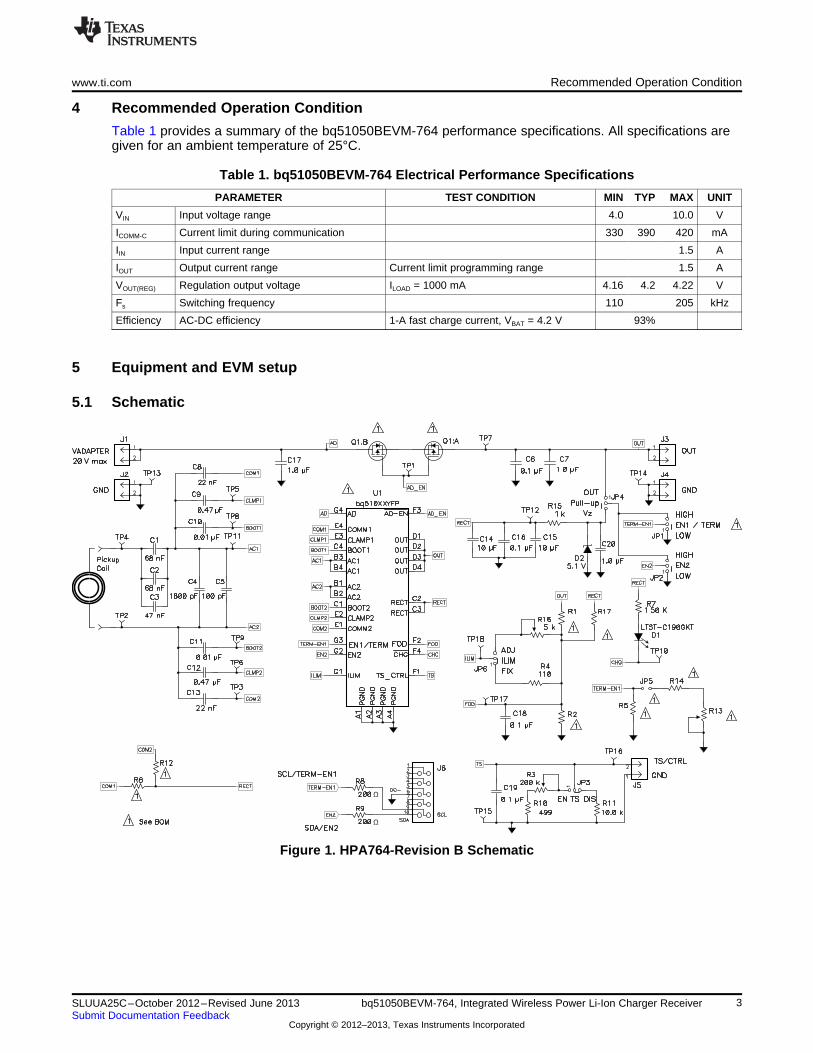
5.1 Schematic
Figure 1. HPA764-Revision B Schematic
3SLUUA25C–October 2012–Revised June 2013 bq51050BEVM-764, Integrated Wireless Power Li-Ion Charger ReceiverSubmit Documentation Feedback
Copyright © 2012–2013, Texas Instruments Incorporated
Equipment and EVM setup www.ti.com
5.2 Connector and Test Point Descriptions
The connection points are described in the following paragraphs.
5.2.1 J1 – AD External Adapter Input, J2-GND
Power can not be provided to simulate an external adapter applied to the receiver in this bq51050BEVM-764 (HPA764-002).
5.2.2 J3 – Output Voltage, J4-GND
Output voltage regulation is 4.2 V in wireless power mode up to 1 A; the adapter option is not supported inthis HPA764-002.
5.2.3 J5 – TS and Return Connector
External connection for temperature sense resistor, see the datasheet for additional information.
5.2.4 J6 – Programming Connector
This connector is populated and is only useful at the factory level for programming the IC.
5.3 Jumpers and Switches
The control jumpers are described in the following paragraphs.
5.3.1 JP1 – EN1 Enable 1
Not populated in this EVM (HPA764-002).
5.3.2 JP2 – EN2 Enable 2
Enable signal input that allows the system to assert wireless charging. If EN2 is set to low, wirelesscharging is enabled unless AD voltage > 3.6 V. If EN2 is set to High, AD mode disabled, wireless chargingalways enabled. Used when OTG plus wireless charging is active.
5.3.3 JP3 – TS Enable or Disable
This jumper enables the TS adjustment feature using R3. The disable position sets voltage at the TS pinto a safe value. The default shorting jumper setting is disabled.
5.3.4 JP4 – Pull-Up to Out or Vz
EN2 pull-up can be powered from OUT or RECT. Vz is derived from RECT through a resistor and Zenerdiode D2.
5.3.5 JP5 – Termination
This jumper, along with R14 and R13, sets the termination current. See the bq51050B datasheet foradditional information. The default shorting jumper setting is installed.
5.3.6 JP6 – ILIM Fix or ADJ
Max output current is set by ILIM pin. In the FIX position, the current is set to a fixed value. In the ADJposition the current is set by R16.
5.4 Test Point Descriptions
The test points are described in the following paragraphs.
4 bq51050BEVM-764, Integrated Wireless Power Li-Ion Charger Receiver SLUUA25C–October 2012–Revised June 2013Submit Documentation Feedback
Copyright © 2012–2013, Texas Instruments Incorporated

www.ti.com Equipment and EVM setup
5.4.1 TP1 – AD-EN
This push-pull driver for the external PFET connects the adapter and the output from the bq5101x. This isnot useful for the bq5105x.
5.4.2 TP2 – AC Input 2
This is the test point for measuring AC voltage applied to the EVM from the receiver coil.
5.4.3 TP3 – COM2 Communication 2 Drive
Communication driver signal, open-drain output connected to communication capacitor.
5.4.4 TP4 – AC Input 1
This is the test point for measuring AC voltage applied to the EVM from the receiver coil.
5.4.5 TP5 – CLMP 1
Overvoltage clamp driver signal, open-drain output is connected to OVP capacitor.
5.4.6 TP6 – CLMP 2
Overvoltage clamp drive signal, open-drain output is connected to OVP capacitor.
5.4.7 TP7 – OUT Output Voltage
This test point is the output voltage from the bq51050B.
5.4.8 TP8 – Boot-1 Boot Capacitor
This bootstrap capacitor 1 drive connects to the integrated circuit (IC).
5.4.9 TP9 – Boot-2 Boot Capacitor
This bootstrap capacitor 2 drive connects to the IC.
5.4.10 TP10 – CHG Charge
This output signal indicates that the output current is being delivered to OUT, the open-drain output.
5.4.11 TP11 – AC1 IC input
This is the AC input to the IC from series capacitors.
5.4.12 TP12 – Rectified Voltage
The input AC voltage is rectified into unregulated DC voltage; additional capacitance is used to filter thevoltage before the regulator.
5.4.13 TP13, TP14, TP15 – GND
These are the ground test points.
5.4.14 TP16 – TS Temp Sensor
This is the connection point for external thermistor; see the data sheet for additional information.
5.4.15 TP17 – FET Open Detection (FOD)
Input for rectified power measurement, pin F2 of the IC. FOD for the bq51050B.
5SLUUA25C–October 2012–Revised June 2013 bq51050BEVM-764, Integrated Wireless Power Li-Ion Charger ReceiverSubmit Documentation Feedback
Copyright © 2012–2013, Texas Instruments Incorporated
Test Procedure www.ti.com
5.4.16 TP18– ILIM
Programming pin for over current limit, pin G1 of the IC.
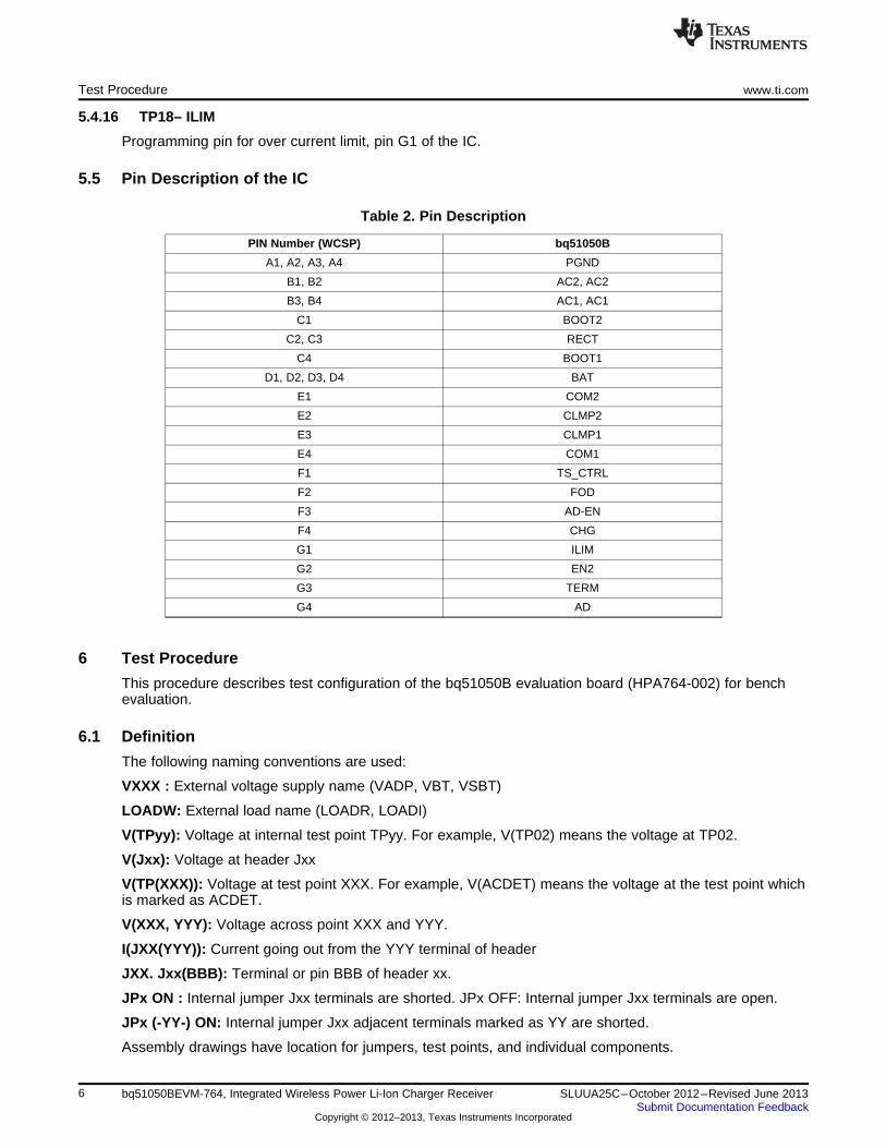
5.5 Pin Description of the IC
Table 2. Pin Description
PIN Number (WCSP) bq51050B
A1, A2, A3, A4 PGND
B1, B2 AC2, AC2
B3, B4 AC1, AC1
C1 BOOT2
C2, C3 RECT
C4 BOOT1
D1, D2, D3, D4 BAT
E1 COM2
E2 CLMP2
E3 CLMP1
E4 COM1
F1 TS_CTRL
F2 FOD
F3 AD-EN
F4 CHG
G1 ILIM
G2 EN2
G3 TERM
G4 AD
6 Test Procedure
This procedure describes test configuration of the bq51050B evaluation board (HPA764-002) for benchevaluation.
6.1 Definition
The following naming conventions are used:
VXXX : External voltage supply name (VADP, VBT, VSBT)
LOADW: External load name (LOADR, LOADI)
V(TPyy): Voltage at internal test point TPyy. For example, V(TP02) means the voltage at TP02.
V(Jxx): Voltage at header Jxx
V(TP(XXX)): Voltage at test point XXX. For example, V(ACDET) means the voltage at the test point whichis marked as ACDET.
V(XXX, YYY): Voltage across point XXX and YYY.
I(JXX(YYY)): Current going out from the YYY terminal of header
JXX. Jxx(BBB): Terminal or pin BBB of header xx.
JPx ON : Internal jumper Jxx terminals are shorted. JPx OFF: Internal jumper Jxx terminals are open.
JPx (-YY-) ON: Internal jumper Jxx adjacent terminals marked as YY are shorted.
Assembly drawings have location for jumpers, test points, and individual components.
6 bq51050BEVM-764, Integrated Wireless Power Li-Ion Charger Receiver SLUUA25C–October 2012–Revised June 2013Submit Documentation Feedback
Copyright © 2012–2013, Texas Instruments Incorporated
Wireless
Transmitter
A
VPS bq51050BEVM
HPA764-002 PR1010
A
V
VOUT
GND
VIN
GND
www.ti.com Test Procedure
6.2 Recommended Test Equipment
The following equipment is needed to complete this test procedure.
6.2.1 Power Supplies
Two power supplies
• Power supply #1 (PS #1) capable of supplying 19 V at 1 A is required
• Power supply #2 (PS #2) capable of supplying up to 6 V at 5 A is required to power the batteryemulator.
6.2.2 Battery Emulator PR1010-002
Use the battery emulator shown in Figure 3 as a battery to test the charger.
6.2.3 Meters
Two DC voltmeters, one multimeter (Ohmmeter), and two DC ammeters are required.
6.2.4 Oscilloscopes
Not required. But can replace the multimeters
6.2.5 bqTesla Transmitter
Power for the bq510xxxEVM-764 receiver EVM is supplied through a bqTESLA transmitter(bq500210EVM-689) or WPC-certified transmitter. The input AC voltage is applied to the receiver throughthe coil located in the receiver bottom.
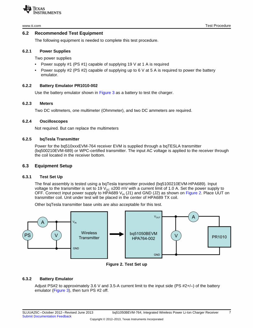
6.3 Equipment Setup
6.3.1 Test Set Up
The final assembly is tested using a bqTesla transmitter provided (bq5100210EVM-HPA689). Inputvoltage to the transmitter is set to 19 VDC ±200 mV with a current limit of 1.0 A. Set the power supply toOFF. Connect input power supply to HPA689 VIN (J1) and GND (J2) as shown on Figure 2. Place UUT ontransmitter coil. Unit under test will be placed in the center of HPA689 TX coil.
Other bqTesla transmitter base units are also acceptable for this test.
Figure 2. Test Set up
6.3.2 Battery Emulator
Adjust PS#2 to approximately 3.6 V and 3.5-A current limit to the input side (PS #2+/–) of the batteryemulator (Figure 3), then turn PS #2 off.
7SLUUA25C–October 2012–Revised June 2013 bq51050BEVM-764, Integrated Wireless Power Li-Ion Charger ReceiverSubmit Documentation Feedback
Copyright © 2012–2013, Texas Instruments Incorporated
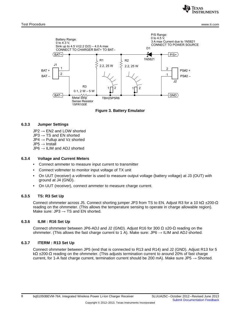
Battery Range:0 to 4.3 V,Sink up to 4.5 V/(2.2 /2) 4.0 A maxΩ –CONNECT TO CHARGER BAT+ TO BAT–
BAT+
BAT–
P/S+
GND
P/S Range:0 to 4.5 V,3 A max Current due to 1N5821CONNECT TO POWER SOURCE
D1
1N5821
2
1
J2
PS#2 +
PS#2 –
R2
2.2, 25 W
1 21 2
TBH25P5R6
R1
2.2, 25 W
R3
0.1, 2 W 5 W–
Metal StripSense Resistor15FR100E
1
2
J1
BAT +
BAT –
Test Procedure www.ti.com
Figure 3. Battery Emulator
6.3.3 Jumper Settings
JP2 → EN2 and LOW shortedJP3 → TS and EN shortedJP4 → Pullup and Vz shortedJP5 → InstallJP6 → ILIM and ADJ shorted
6.3.4 Voltage and Current Meters• Connect ammeter to measure input current to transmitter
• Connect voltmeter to monitor input voltage of TX unit
• On UUT (receiver) a voltmeter is used to measure output voltage (battery voltage) at J3 (OUT) withground at J4 (GND).
• On UUT (receiver), connect ammeter to measure charge current.
6.3.5 TS: R3 Set Up
Connect ohmmeter across J5. Connect shorting jumper JP3 from TS to EN. Adjust R3 for a 10 kΩ ±200-Ωreading on the ohmmeter. (This allows the temperature sensing to operate in charge allowable region).Make sure: JP3 → TS and EN shorted.
6.3.6 ILIM : R16 Set Up
Connect ohmmeter between JP6-ADJ and J2 (GND). Adjust R16 for 300 Ω ±20-Ω reading on theohmmeter. (This allows the fast charge current to 1 A). Make sure: JP6 → ILIM and ADJ shorted.
6.3.7 ITERM : R13 Set Up
Connect ohmmeter between JP5 (end that is connected to R13 and R14) and J2 (GND). Adjust R13 for 5kΩ ±200-Ω reading on the ohmmeter. (This adjusts termination current to around 20% of fast chargecurrent, for 1-A fast charge current, termination current should be 200 mA). Make sure JP5 → Shorted.
8 bq51050BEVM-764, Integrated Wireless Power Li-Ion Charger Receiver SLUUA25C–October 2012–Revised June 2013Submit Documentation Feedback
Copyright © 2012–2013, Texas Instruments Incorporated
www.ti.com Test Procedure
6.4 Procedure
6.4.1 Turn ON Operation• Turn ON transmitter PS#1 (19 V)
• Transmitter – verify LED D2 is ON
• Turn ON emulator PS#2 (3.6 V)
• Put the receiver EVM on the transmitter coil and align them correctly
• After 5 s, verify that:
1. Transmitter – status LED D5 is flashing green ~ 1 s
2. You should hear a beep from the transmitter
3. Transmitter – LED D2 still ON
4. Receiver – LED D1 is ON
6.4.2 Pre-Charge Operation• Adjust PS#2 to read 2.5 V across J3 and J4 (battery voltage)
• Verify the charging current is 200 mA ±20 mA
6.4.3 Fast-Charge Operation• Adjust PS#2 to read 3.6 V across J3 and J4 (battery voltage).
• Verify the charging current is 1000 mA ±100 mA
6.4.4 Constant Voltage Charge Operation and Termination• Adjust PS#2 to read 4.2 V ±50 mV across J3 and J4 ( Battery Voltage)
• Keep increasing the voltage on PS#2 and observe the charging current decreases (constant voltagephase)
• Keep increasing the voltage on PS#2 until you reach and observe the charging current approximately200 mA ± 20 mA (constant voltage phase)
• The charge should terminate after you reach the 200 mA ±200mA level
6.4.5 Efficiency Test• Adjust PS#2 to read 3.6 V ±50 mV across J3 and J4 ( Battery Voltage)
• Remove the receiver and reinstall it
• Verify the charging current is 1000 mA ±100 mA
• Verify that input current to TX is less than 350 mA ±30 mA with input voltage at 19 VDC
9SLUUA25C–October 2012–Revised June 2013 bq51050BEVM-764, Integrated Wireless Power Li-Ion Charger ReceiverSubmit Documentation Feedback
Copyright © 2012–2013, Texas Instruments Incorporated

5 V/div
TP2-AC-IN
TP12-V-RECT
I-BAT
5 V/div
1 A/div
200 ms/div
5 V/div
TP2-AC-IN
TP12-V-RECT
I-BAT
5 V/div
1 A/div
200 ms/div
Test Results www.ti.com
7 Test Results
7.1 Start up to Fast-Charge Mode
With the power supply off, connect supply to the bqTESLA transmitter.
• Place the bqTESLA receiver on the transmitter
• Connect battery emulator to J3 with GND J4
• Power TX with 19 V
• Trigger scope sweep on I-BAT
The test results shown in Figure 4 are taken under 19-V input, 3.7-V battery and 1000-mA fast chargecurrent.
Figure 4. Start-Up to Fast-Charge Mode
7.2 Start up to Pre-Charge Mode
With the power supply off, connect the supply to the bqTESLA transmitter.
• Place the bqTESLA receiver on the transmitter
• Connect the battery emulator to J3 with GND J4
• Power TX with 19 V
• Trigger scope sweep on I-BAT
The test results shown in Figure 5 are taken under 19-V input, 2-V battery and 200-mA pre-chargecurrent.
Figure 5. Start-Up to Pre-charge Mode
10 bq51050BEVM-764, Integrated Wireless Power Li-Ion Charger Receiver SLUUA25C–October 2012–Revised June 2013Submit Documentation Feedback
Copyright © 2012–2013, Texas Instruments Incorporated

TP2-AC-IN
TP12-V-RECT
I-BAT
5 V/div
5 V/div
1 A/div
1 s/div
5 V/div
TP2-AC-IN
TP12-V-RECT
I-BAT
5 V/div
1 A/div
500 ms/div
www.ti.com Test Results
7.3 Pre-charge to Fast-Charge Transition
With the power supply off, connect the supply to the bqTESLA transmitter.
• Place the bqTESLA receiver on the transmitter
• Connect the battery emulator to J3 with GND J4
• Power TX with 19 V
• Adjust the battery emulator voltage to 2 V (pre-charge mode)
• Increase the battery emulator voltage until exiting the pre-charge mode (200 mA) and enter fast-chargemode (1000 mA)
• Trigger scope sweep on I-BAT
The test results shown in Figure 6 shows pre-charge to fast-charge mode transition
Figure 6. Pre-charge to Fast-Charge Transition
7.4 Fast Charge to Taper and Termination Transition
With the power supply off, connect the supply to the bqTESLA transmitter.
• Place the bqTESLA receiver on the transmitter
• Connect the battery emulator to J3 with GND J4
• Power TX with 19 V
• Adjust the battery emulator voltage to 4.2 V (fast-charge mode, 1000 mA)
• Decrease the battery emulator voltage until exiting the fast-charge mode to taper and then termination200 mA
• Trigger scope sweep on I-BAT
The test results shown in Figure 7 shows fast-charge to taper and termination modes transition.
Figure 7. Fast Charge to Taper and Termination Transition
11SLUUA25C–October 2012–Revised June 2013 bq51050BEVM-764, Integrated Wireless Power Li-Ion Charger ReceiverSubmit Documentation Feedback
Copyright © 2012–2013, Texas Instruments Incorporated
80
82
84
86
88
90
92
94
96
98
100
100 200 300 400 500 600 700 800 900 1000 1100
Effi
cien
cy (
%)
ICHG (mA)
bq51050B
C002
0
10
20
30
40
50
60
70
80
90
100
0.00 0.50 1.00 1.50 2.00 2.50 3.00 3.50 4.00 4.50
Effi
cien
cy %
)
Power (W)
bq51050B
C001
Test Results www.ti.com
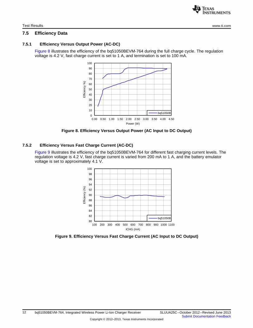
7.5 Efficiency Data
7.5.1 Efficiency Versus Output Power (AC-DC)
Figure 8 illustrates the efficiency of the bq51050BEVM-764 during the full charge cycle. The regulationvoltage is 4.2 V, fast charge current is set to 1 A, and termination is set to 100 mA.
Figure 8. Efficiency Versus Output Power (AC Input to DC Output)
7.5.2 Efficiency Versus Fast Charge Current (AC-DC)
Figure 9 illustrates the efficiency of the bq51050BEVM-764 for different fast charging current levels. Theregulation voltage is 4.2 V, fast charge current is varied from 200 mA to 1 A, and the battery emulatorvoltage is set to approximately 4.1 V.
Figure 9. Efficiency Versus Fast Charge Current (AC Input to DC Output)
12 bq51050BEVM-764, Integrated Wireless Power Li-Ion Charger Receiver SLUUA25C–October 2012–Revised June 2013Submit Documentation Feedback
Copyright © 2012–2013, Texas Instruments Incorporated
www.ti.com Test Results
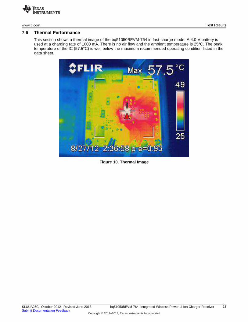
7.6 Thermal Performance
This section shows a thermal image of the bq51050BEVM-764 in fast-charge mode. A 4.0-V battery isused at a charging rate of 1000 mA. There is no air flow and the ambient temperature is 25°C. The peaktemperature of the IC (57.5°C) is well below the maximum recommended operating condition listed in thedata sheet.
Figure 10. Thermal Image
13SLUUA25C–October 2012–Revised June 2013 bq51050BEVM-764, Integrated Wireless Power Li-Ion Charger ReceiverSubmit Documentation Feedback
Copyright © 2012–2013, Texas Instruments Incorporated
Layout and Bill of Material www.ti.com
8 Layout and Bill of Material
8.1 Layout
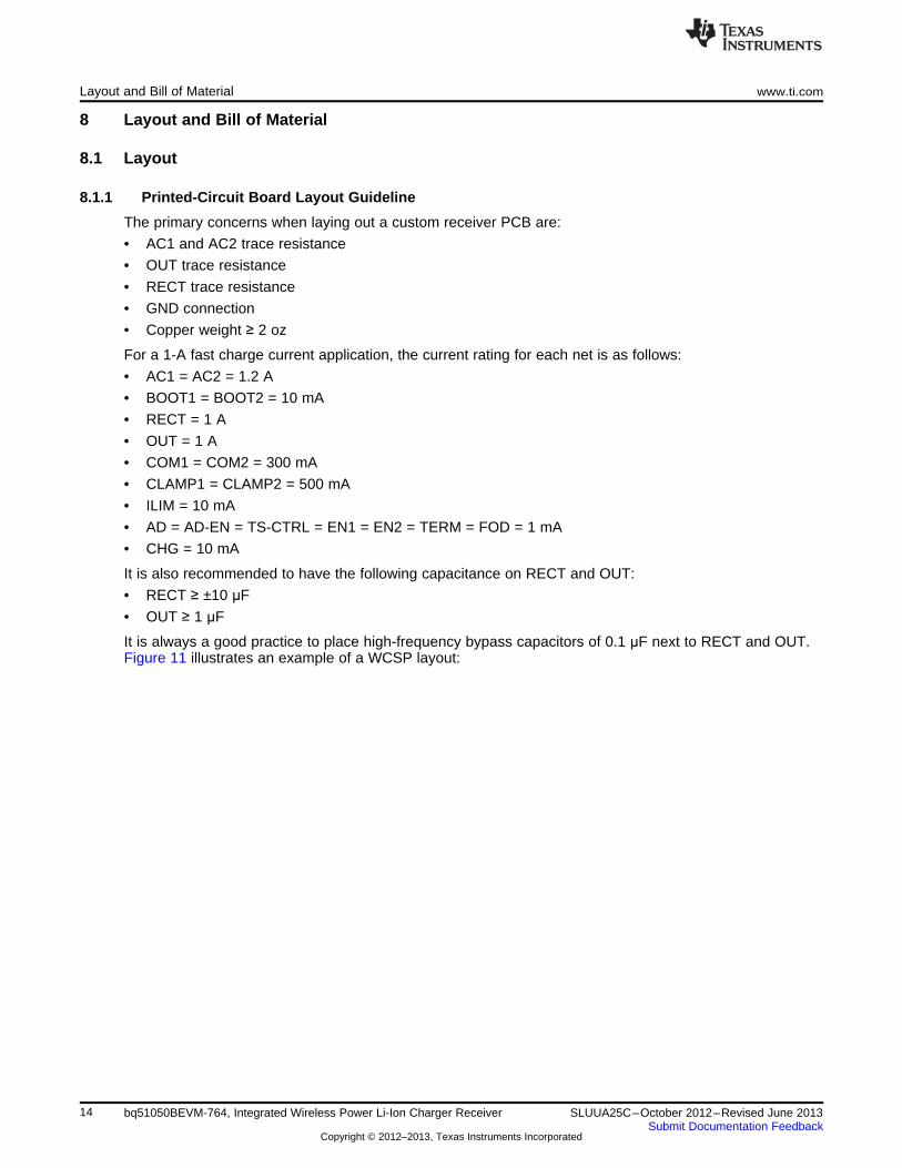
8.1.1 Printed-Circuit Board Layout Guideline
The primary concerns when laying out a custom receiver PCB are:
• AC1 and AC2 trace resistance
• OUT trace resistance
• RECT trace resistance
• GND connection
• Copper weight ≥ 2 oz
For a 1-A fast charge current application, the current rating for each net is as follows:
• AC1 = AC2 = 1.2 A
• BOOT1 = BOOT2 = 10 mA
• RECT = 1 A
• OUT = 1 A
• COM1 = COM2 = 300 mA
• CLAMP1 = CLAMP2 = 500 mA
• ILIM = 10 mA
• AD = AD-EN = TS-CTRL = EN1 = EN2 = TERM = FOD = 1 mA
• CHG = 10 mA
It is also recommended to have the following capacitance on RECT and OUT:
• RECT ≥ ±10 μF
• OUT ≥ 1 μF
It is always a good practice to place high-frequency bypass capacitors of 0.1 μF next to RECT and OUT.Figure 11 illustrates an example of a WCSP layout:
14 bq51050BEVM-764, Integrated Wireless Power Li-Ion Charger Receiver SLUUA25C–October 2012–Revised June 2013Submit Documentation Feedback
Copyright © 2012–2013, Texas Instruments Incorporated
www.ti.com Layout and Bill of Material
Figure 11. bq51050BEVM Layout Example
15SLUUA25C–October 2012–Revised June 2013 bq51050BEVM-764, Integrated Wireless Power Li-Ion Charger ReceiverSubmit Documentation Feedback
Copyright © 2012–2013, Texas Instruments Incorporated
Layout and Bill of Material www.ti.com
8.1.2 Layout
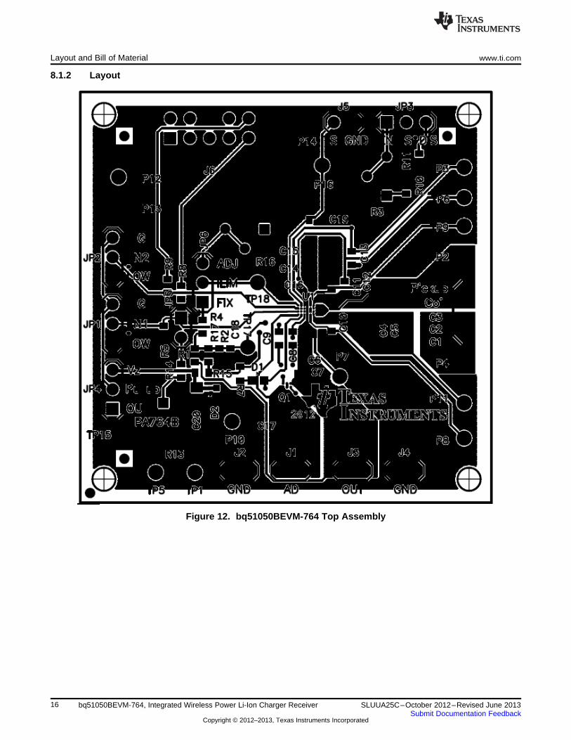
Figure 12. bq51050BEVM-764 Top Assembly
16 bq51050BEVM-764, Integrated Wireless Power Li-Ion Charger Receiver SLUUA25C–October 2012–Revised June 2013Submit Documentation Feedback
Copyright © 2012–2013, Texas Instruments Incorporated
www.ti.com Layout and Bill of Material
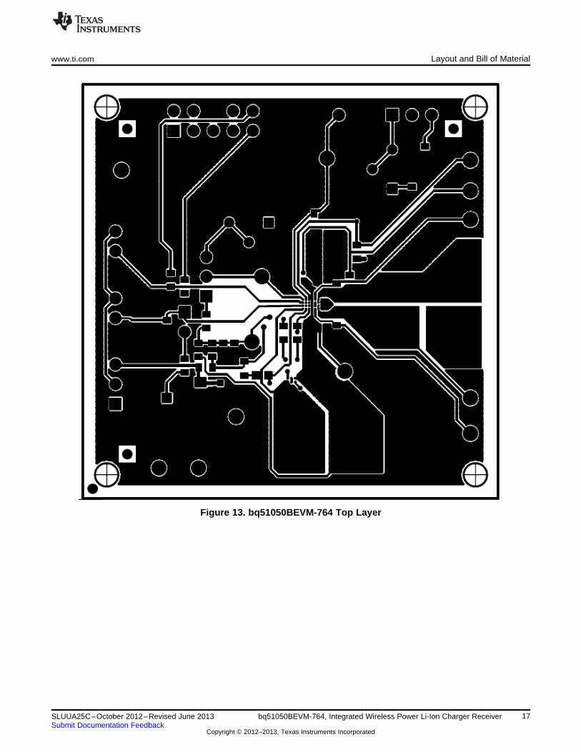
Figure 13. bq51050BEVM-764 Top Layer
17SLUUA25C–October 2012–Revised June 2013 bq51050BEVM-764, Integrated Wireless Power Li-Ion Charger ReceiverSubmit Documentation Feedback
Copyright © 2012–2013, Texas Instruments Incorporated
Layout and Bill of Material www.ti.com
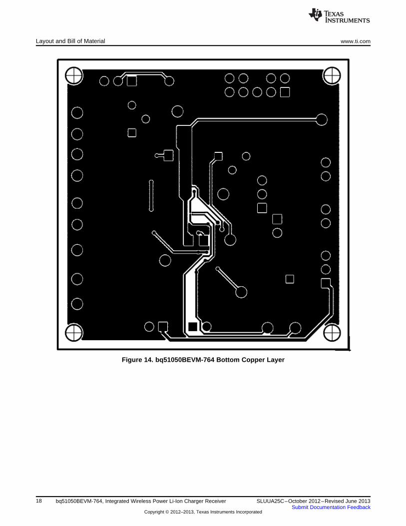
Figure 14. bq51050BEVM-764 Bottom Copper Layer
18 bq51050BEVM-764, Integrated Wireless Power Li-Ion Charger Receiver SLUUA25C–October 2012–Revised June 2013Submit Documentation Feedback
Copyright © 2012–2013, Texas Instruments Incorporated
www.ti.com Layout and Bill of Material
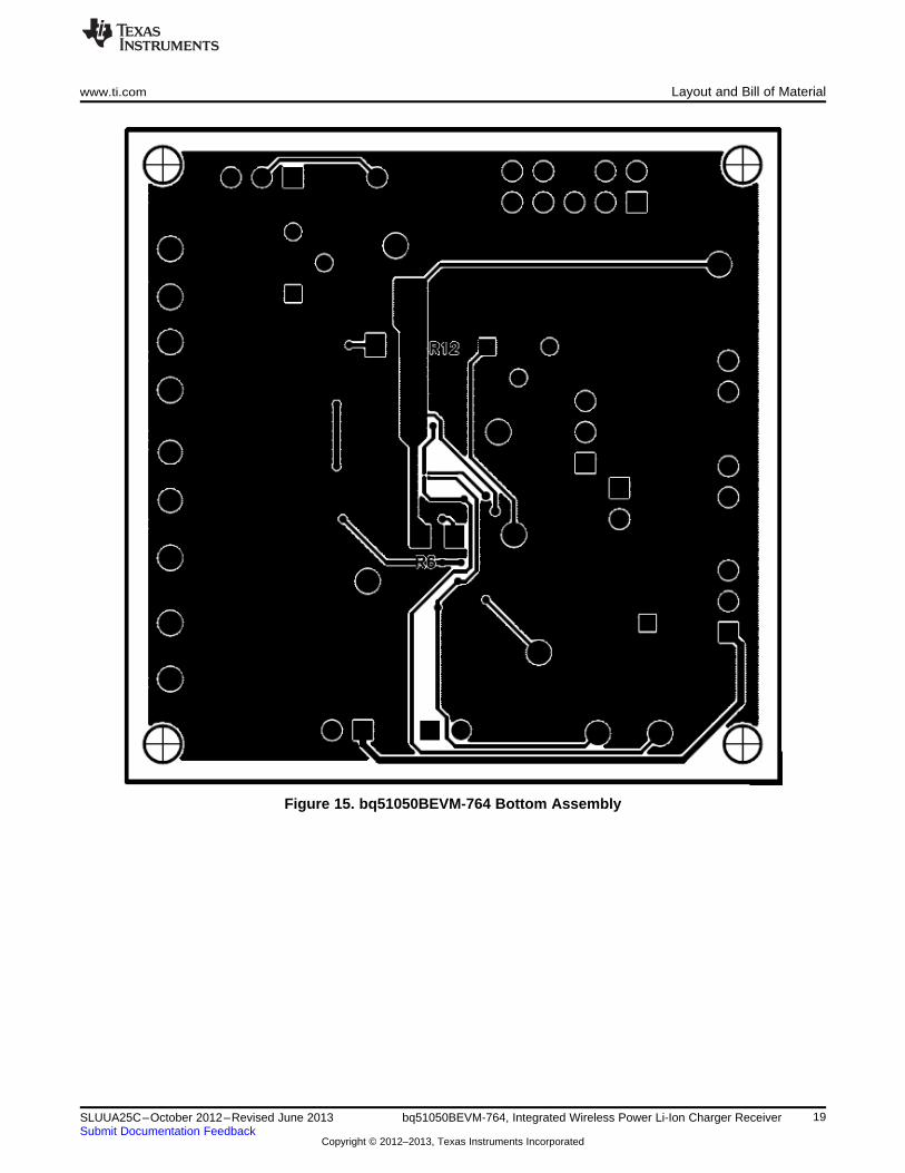
Figure 15. bq51050BEVM-764 Bottom Assembly
19SLUUA25C–October 2012–Revised June 2013 bq51050BEVM-764, Integrated Wireless Power Li-Ion Charger ReceiverSubmit Documentation Feedback
Copyright © 2012–2013, Texas Instruments Incorporated
Layout and Bill of Material www.ti.com
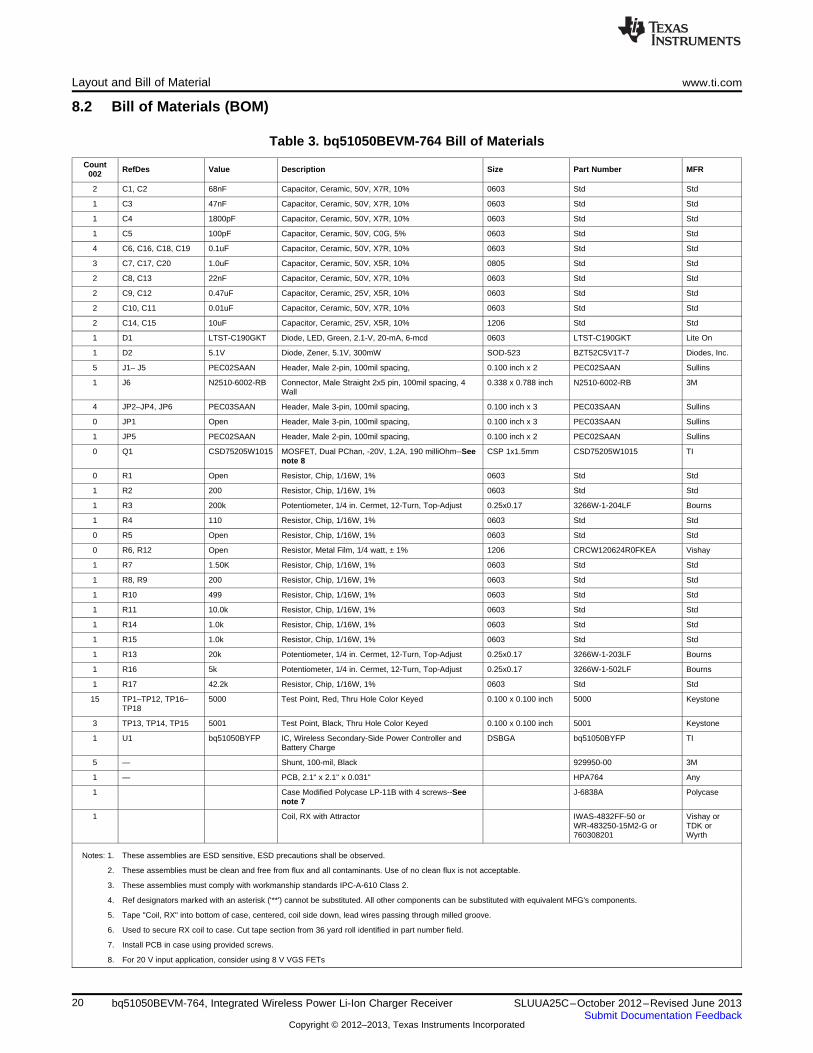
8.2 Bill of Materials (BOM)
Table 3. bq51050BEVM-764 Bill of Materials
Count RefDes Value Description Size Part Number MFR002
2 C1, C2 68nF Capacitor, Ceramic, 50V, X7R, 10% 0603 Std Std
1 C3 47nF Capacitor, Ceramic, 50V, X7R, 10% 0603 Std Std
1 C4 1800pF Capacitor, Ceramic, 50V, X7R, 10% 0603 Std Std
1 C5 100pF Capacitor, Ceramic, 50V, C0G, 5% 0603 Std Std
4 C6, C16, C18, C19 0.1uF Capacitor, Ceramic, 50V, X7R, 10% 0603 Std Std
3 C7, C17, C20 1.0uF Capacitor, Ceramic, 50V, X5R, 10% 0805 Std Std
2 C8, C13 22nF Capacitor, Ceramic, 50V, X7R, 10% 0603 Std Std
2 C9, C12 0.47uF Capacitor, Ceramic, 25V, X5R, 10% 0603 Std Std
2 C10, C11 0.01uF Capacitor, Ceramic, 50V, X7R, 10% 0603 Std Std
2 C14, C15 10uF Capacitor, Ceramic, 25V, X5R, 10% 1206 Std Std
1 D1 LTST-C190GKT Diode, LED, Green, 2.1-V, 20-mA, 6-mcd 0603 LTST-C190GKT Lite On
1 D2 5.1V Diode, Zener, 5.1V, 300mW SOD-523 BZT52C5V1T-7 Diodes, Inc.
5 J1– J5 PEC02SAAN Header, Male 2-pin, 100mil spacing, 0.100 inch x 2 PEC02SAAN Sullins
1 J6 N2510-6002-RB Connector, Male Straight 2x5 pin, 100mil spacing, 4 0.338 x 0.788 inch N2510-6002-RB 3MWall
4 JP2–JP4, JP6 PEC03SAAN Header, Male 3-pin, 100mil spacing, 0.100 inch x 3 PEC03SAAN Sullins
0 JP1 Open Header, Male 3-pin, 100mil spacing, 0.100 inch x 3 PEC03SAAN Sullins
1 JP5 PEC02SAAN Header, Male 2-pin, 100mil spacing, 0.100 inch x 2 PEC02SAAN Sullins
0 Q1 CSD75205W1015 MOSFET, Dual PChan, -20V, 1.2A, 190 milliOhm--See CSP 1x1.5mm CSD75205W1015 TInote 8
0 R1 Open Resistor, Chip, 1/16W, 1% 0603 Std Std
1 R2 200 Resistor, Chip, 1/16W, 1% 0603 Std Std
1 R3 200k Potentiometer, 1/4 in. Cermet, 12-Turn, Top-Adjust 0.25x0.17 3266W-1-204LF Bourns
1 R4 110 Resistor, Chip, 1/16W, 1% 0603 Std Std
0 R5 Open Resistor, Chip, 1/16W, 1% 0603 Std Std
0 R6, R12 Open Resistor, Metal Film, 1/4 watt, ± 1% 1206 CRCW120624R0FKEA Vishay
1 R7 1.50K Resistor, Chip, 1/16W, 1% 0603 Std Std
1 R8, R9 200 Resistor, Chip, 1/16W, 1% 0603 Std Std
1 R10 499 Resistor, Chip, 1/16W, 1% 0603 Std Std
1 R11 10.0k Resistor, Chip, 1/16W, 1% 0603 Std Std
1 R14 1.0k Resistor, Chip, 1/16W, 1% 0603 Std Std
1 R15 1.0k Resistor, Chip, 1/16W, 1% 0603 Std Std
1 R13 20k Potentiometer, 1/4 in. Cermet, 12-Turn, Top-Adjust 0.25x0.17 3266W-1-203LF Bourns
1 R16 5k Potentiometer, 1/4 in. Cermet, 12-Turn, Top-Adjust 0.25x0.17 3266W-1-502LF Bourns
1 R17 42.2k Resistor, Chip, 1/16W, 1% 0603 Std Std
15 TP1–TP12, TP16– 5000 Test Point, Red, Thru Hole Color Keyed 0.100 x 0.100 inch 5000 KeystoneTP18
3 TP13, TP14, TP15 5001 Test Point, Black, Thru Hole Color Keyed 0.100 x 0.100 inch 5001 Keystone
1 U1 bq51050BYFP IC, Wireless Secondary-Side Power Controller and DSBGA bq51050BYFP TIBattery Charge
5 — Shunt, 100-mil, Black 929950-00 3M
1 — PCB, 2.1" x 2.1" x 0.031" HPA764 Any
1 Case Modified Polycase LP-11B with 4 screws--See J-6838A Polycasenote 7
1 Coil, RX with Attractor IWAS-4832FF-50 or Vishay orWR-483250-15M2-G or TDK or760308201 Wyrth
Notes: 1. These assemblies are ESD sensitive, ESD precautions shall be observed.
2. These assemblies must be clean and free from flux and all contaminants. Use of no clean flux is not acceptable.
3. These assemblies must comply with workmanship standards IPC-A-610 Class 2.
4. Ref designators marked with an asterisk ('**') cannot be substituted. All other components can be substituted with equivalent MFG's components.
5. Tape "Coil, RX" into bottom of case, centered, coil side down, lead wires passing through milled groove.
6. Used to secure RX coil to case. Cut tape section from 36 yard roll identified in part number field.
7. Install PCB in case using provided screws.
8. For 20 V input application, consider using 8 V VGS FETs
20 bq51050BEVM-764, Integrated Wireless Power Li-Ion Charger Receiver SLUUA25C–October 2012–Revised June 2013Submit Documentation Feedback
Copyright © 2012–2013, Texas Instruments Incorporated
EVALUATION BOARD/KIT/MODULE (EVM) ADDITIONAL TERMS
Texas Instruments (TI) provides the enclosed Evaluation Board/Kit/Module (EVM) under the following conditions:
The user assumes all responsibility and liability for proper and safe handling of the goods. Further, the user indemnifies TI from all claimsarising from the handling or use of the goods.
Should this evaluation board/kit not meet the specifications indicated in the User’s Guide, the board/kit may be returned within 30 days fromthe date of delivery for a full refund. THE FOREGOING LIMITED WARRANTY IS THE EXCLUSIVE WARRANTY MADE BY SELLER TOBUYER AND IS IN LIEU OF ALL OTHER WARRANTIES, EXPRESSED, IMPLIED, OR STATUTORY, INCLUDING ANY WARRANTY OFMERCHANTABILITY OR FITNESS FOR ANY PARTICULAR PURPOSE. EXCEPT TO THE EXTENT OF THE INDEMNITY SET FORTHABOVE, NEITHER PARTY SHALL BE LIABLE TO THE OTHER FOR ANY INDIRECT, SPECIAL, INCIDENTAL, OR CONSEQUENTIALDAMAGES.
Please read the User's Guide and, specifically, the Warnings and Restrictions notice in the User's Guide prior to handling the product. Thisnotice contains important safety information about temperatures and voltages. For additional information on TI's environmental and/or safetyprograms, please visit www.ti.com/esh or contact TI.
No license is granted under any patent right or other intellectual property right of TI covering or relating to any machine, process, orcombination in which such TI products or services might be or are used. TI currently deals with a variety of customers for products, andtherefore our arrangement with the user is not exclusive. TI assumes no liability for applications assistance, customer product design,software performance, or infringement of patents or services described herein.
REGULATORY COMPLIANCE INFORMATION
As noted in the EVM User’s Guide and/or EVM itself, this EVM and/or accompanying hardware may or may not be subject to the FederalCommunications Commission (FCC) and Industry Canada (IC) rules.
For EVMs not subject to the above rules, this evaluation board/kit/module is intended for use for ENGINEERING DEVELOPMENT,DEMONSTRATION OR EVALUATION PURPOSES ONLY and is not considered by TI to be a finished end product fit for general consumeruse. It generates, uses, and can radiate radio frequency energy and has not been tested for compliance with the limits of computingdevices pursuant to part 15 of FCC or ICES-003 rules, which are designed to provide reasonable protection against radio frequencyinterference. Operation of the equipment may cause interference with radio communications, in which case the user at his own expense willbe required to take whatever measures may be required to correct this interference.
General Statement for EVMs including a radio
User Power/Frequency Use Obligations: This radio is intended for development/professional use only in legally allocated frequency andpower limits. Any use of radio frequencies and/or power availability of this EVM and its development application(s) must comply with locallaws governing radio spectrum allocation and power limits for this evaluation module. It is the user’s sole responsibility to only operate thisradio in legally acceptable frequency space and within legally mandated power limitations. Any exceptions to this are strictly prohibited andunauthorized by Texas Instruments unless user has obtained appropriate experimental/development licenses from local regulatoryauthorities, which is responsibility of user including its acceptable authorization.
For EVMs annotated as FCC – FEDERAL COMMUNICATIONS COMMISSION Part 15 Compliant
Caution
This device complies with part 15 of the FCC Rules. Operation is subject to the following two conditions: (1) This device may not causeharmful interference, and (2) this device must accept any interference received, including interference that may cause undesired operation.
Changes or modifications not expressly approved by the party responsible for compliance could void the user's authority to operate theequipment.
FCC Interference Statement for Class A EVM devices
This equipment has been tested and found to comply with the limits for a Class A digital device, pursuant to part 15 of the FCC Rules.These limits are designed to provide reasonable protection against harmful interference when the equipment is operated in a commercialenvironment. This equipment generates, uses, and can radiate radio frequency energy and, if not installed and used in accordance with theinstruction manual, may cause harmful interference to radio communications. Operation of this equipment in a residential area is likely tocause harmful interference in which case the user will be required to correct the interference at his own expense.

FCC Interference Statement for Class B EVM devices
This equipment has been tested and found to comply with the limits for a Class B digital device, pursuant to part 15 of the FCC Rules.These limits are designed to provide reasonable protection against harmful interference in a residential installation. This equipmentgenerates, uses and can radiate radio frequency energy and, if not installed and used in accordance with the instructions, may causeharmful interference to radio communications. However, there is no guarantee that interference will not occur in a particular installation. Ifthis equipment does cause harmful interference to radio or television reception, which can be determined by turning the equipment off andon, the user is encouraged to try to correct the interference by one or more of the following measures:
• Reorient or relocate the receiving antenna.• Increase the separation between the equipment and receiver.• Connect the equipment into an outlet on a circuit different from that to which the receiver is connected.• Consult the dealer or an experienced radio/TV technician for help.
For EVMs annotated as IC – INDUSTRY CANADA Compliant
This Class A or B digital apparatus complies with Canadian ICES-003.
Changes or modifications not expressly approved by the party responsible for compliance could void the user’s authority to operate theequipment.
Concerning EVMs including radio transmitters
This device complies with Industry Canada licence-exempt RSS standard(s). Operation is subject to the following two conditions: (1) thisdevice may not cause interference, and (2) this device must accept any interference, including interference that may cause undesiredoperation of the device.
Concerning EVMs including detachable antennas
Under Industry Canada regulations, this radio transmitter may only operate using an antenna of a type and maximum (or lesser) gainapproved for the transmitter by Industry Canada. To reduce potential radio interference to other users, the antenna type and its gain shouldbe so chosen that the equivalent isotropically radiated power (e.i.r.p.) is not more than that necessary for successful communication.
This radio transmitter has been approved by Industry Canada to operate with the antenna types listed in the user guide with the maximumpermissible gain and required antenna impedance for each antenna type indicated. Antenna types not included in this list, having a gaingreater than the maximum gain indicated for that type, are strictly prohibited for use with this device.
Cet appareil numérique de la classe A ou B est conforme à la norme NMB-003 du Canada.
Les changements ou les modifications pas expressément approuvés par la partie responsable de la conformité ont pu vider l’autorité del'utilisateur pour actionner l'équipement.
Concernant les EVMs avec appareils radio
Le présent appareil est conforme aux CNR d'Industrie Canada applicables aux appareils radio exempts de licence. L'exploitation estautorisée aux deux conditions suivantes : (1) l'appareil ne doit pas produire de brouillage, et (2) l'utilisateur de l'appareil doit accepter toutbrouillage radioélectrique subi, même si le brouillage est susceptible d'en compromettre le fonctionnement.
Concernant les EVMs avec antennes détachables
Conformément à la réglementation d'Industrie Canada, le présent émetteur radio peut fonctionner avec une antenne d'un type et d'un gainmaximal (ou inférieur) approuvé pour l'émetteur par Industrie Canada. Dans le but de réduire les risques de brouillage radioélectrique àl'intention des autres utilisateurs, il faut choisir le type d'antenne et son gain de sorte que la puissance isotrope rayonnée équivalente(p.i.r.e.) ne dépasse pas l'intensité nécessaire à l'établissement d'une communication satisfaisante.
Le présent émetteur radio a été approuvé par Industrie Canada pour fonctionner avec les types d'antenne énumérés dans le manueld’usage et ayant un gain admissible maximal et l'impédance requise pour chaque type d'antenne. Les types d'antenne non inclus danscette liste, ou dont le gain est supérieur au gain maximal indiqué, sont strictement interdits pour l'exploitation de l'émetteur.
SPACER
SPACER
SPACER
SPACER
SPACER
SPACER
SPACER
SPACER
【【Important Notice for Users of this Product in Japan】】This development kit is NOT certified as Confirming to Technical Regulations of Radio Law of Japan
If you use this product in Japan, you are required by Radio Law of Japan to follow the instructions below with respect to this product:
1. Use this product in a shielded room or any other test facility as defined in the notification #173 issued by Ministry of Internal Affairs andCommunications on March 28, 2006, based on Sub-section 1.1 of Article 6 of the Ministry’s Rule for Enforcement of Radio Law ofJapan,
2. Use this product only after you obtained the license of Test Radio Station as provided in Radio Law of Japan with respect to thisproduct, or
3. Use of this product only after you obtained the Technical Regulations Conformity Certification as provided in Radio Law of Japan withrespect to this product. Also, please do not transfer this product, unless you give the same notice above to the transferee. Please notethat if you could not follow the instructions above, you will be subject to penalties of Radio Law of Japan.
Texas Instruments Japan Limited(address) 24-1, Nishi-Shinjuku 6 chome, Shinjuku-ku, Tokyo, Japan
http://www.tij.co.jp
【ご使用にあたっての注】
本開発キットは技術基準適合証明を受けておりません。
本製品のご使用に際しては、電波法遵守のため、以下のいずれかの措置を取っていただく必要がありますのでご注意ください。1. 電波法施行規則第6条第1項第1号に基づく平成18年3月28日総務省告示第173号で定められた電波暗室等の試験設備でご使用いただく。2. 実験局の免許を取得後ご使用いただく。3. 技術基準適合証明を取得後ご使用いただく。
なお、本製品は、上記の「ご使用にあたっての注意」を譲渡先、移転先に通知しない限り、譲渡、移転できないものとします。
上記を遵守頂けない場合は、電波法の罰則が適用される可能性があることをご留意ください。
日本テキサス・インスツルメンツ株式会社東京都新宿区西新宿6丁目24番1号西新宿三井ビルhttp://www.tij.co.jp
SPACER
SPACER
SPACER
SPACER
SPACER
SPACER
SPACER
SPACER
SPACER
SPACER
SPACER
SPACER
SPACER
SPACER
SPACER
SPACER
SPACER
EVALUATION BOARD/KIT/MODULE (EVM)WARNINGS, RESTRICTIONS AND DISCLAIMERS
For Feasibility Evaluation Only, in Laboratory/Development Environments. Unless otherwise indicated, this EVM is not a finishedelectrical equipment and not intended for consumer use. It is intended solely for use for preliminary feasibility evaluation inlaboratory/development environments by technically qualified electronics experts who are familiar with the dangers and application risksassociated with handling electrical mechanical components, systems and subsystems. It should not be used as all or part of a finished endproduct.
Your Sole Responsibility and Risk. You acknowledge, represent and agree that:
1. You have unique knowledge concerning Federal, State and local regulatory requirements (including but not limited to Food and DrugAdministration regulations, if applicable) which relate to your products and which relate to your use (and/or that of your employees,affiliates, contractors or designees) of the EVM for evaluation, testing and other purposes.
2. You have full and exclusive responsibility to assure the safety and compliance of your products with all such laws and other applicableregulatory requirements, and also to assure the safety of any activities to be conducted by you and/or your employees, affiliates,contractors or designees, using the EVM. Further, you are responsible to assure that any interfaces (electronic and/or mechanical)between the EVM and any human body are designed with suitable isolation and means to safely limit accessible leakage currents tominimize the risk of electrical shock hazard.
3. You will employ reasonable safeguards to ensure that your use of the EVM will not result in any property damage, injury or death, evenif the EVM should fail to perform as described or expected.
4. You will take care of proper disposal and recycling of the EVM’s electronic components and packing materials.
Certain Instructions. It is important to operate this EVM within TI’s recommended specifications and environmental considerations per theuser guidelines. Exceeding the specified EVM ratings (including but not limited to input and output voltage, current, power, andenvironmental ranges) may cause property damage, personal injury or death. If there are questions concerning these ratings please contacta TI field representative prior to connecting interface electronics including input power and intended loads. Any loads applied outside of thespecified output range may result in unintended and/or inaccurate operation and/or possible permanent damage to the EVM and/orinterface electronics. Please consult the EVM User's Guide prior to connecting any load to the EVM output. If there is uncertainty as to theload specification, please contact a TI field representative. During normal operation, some circuit components may have case temperaturesgreater than 60°C as long as the input and output are maintained at a normal ambient operating temperature. These components includebut are not limited to linear regulators, switching transistors, pass transistors, and current sense resistors which can be identified using theEVM schematic located in the EVM User's Guide. When placing measurement probes near these devices during normal operation, pleasebe aware that these devices may be very warm to the touch. As with all electronic evaluation tools, only qualified personnel knowledgeablein electronic measurement and diagnostics normally found in development environments should use these EVMs.
Agreement to Defend, Indemnify and Hold Harmless. You agree to defend, indemnify and hold TI, its licensors and their representativesharmless from and against any and all claims, damages, losses, expenses, costs and liabilities (collectively, "Claims") arising out of or inconnection with any use of the EVM that is not in accordance with the terms of the agreement. This obligation shall apply whether Claimsarise under law of tort or contract or any other legal theory, and even if the EVM fails to perform as described or expected.
Safety-Critical or Life-Critical Applications. If you intend to evaluate the components for possible use in safety critical applications (suchas life support) where a failure of the TI product would reasonably be expected to cause severe personal injury or death, such as deviceswhich are classified as FDA Class III or similar classification, then you must specifically notify TI of such intent and enter into a separateAssurance and Indemnity Agreement.
Mailing Address: Texas Instruments, Post Office Box 655303, Dallas, Texas 75265Copyright © 2013, Texas Instruments Incorporated

IMPORTANT NOTICE
Texas Instruments Incorporated and its subsidiaries (TI) reserve the right to make corrections, enhancements, improvements and otherchanges to its semiconductor products and services per JESD46, latest issue, and to discontinue any product or service per JESD48, latestissue. Buyers should obtain the latest relevant information before placing orders and should verify that such information is current andcomplete. All semiconductor products (also referred to herein as “components”) are sold subject to TI’s terms and conditions of salesupplied at the time of order acknowledgment.
TI warrants performance of its components to the specifications applicable at the time of sale, in accordance with the warranty in TI’s termsand conditions of sale of semiconductor products. Testing and other quality control techniques are used to the extent TI deems necessaryto support this warranty. Except where mandated by applicable law, testing of all parameters of each component is not necessarilyperformed.
TI assumes no liability for applications assistance or the design of Buyers’ products. Buyers are responsible for their products andapplications using TI components. To minimize the risks associated with Buyers’ products and applications, Buyers should provideadequate design and operating safeguards.
TI does not warrant or represent that any license, either express or implied, is granted under any patent right, copyright, mask work right, orother intellectual property right relating to any combination, machine, or process in which TI components or services are used. Informationpublished by TI regarding third-party products or services does not constitute a license to use such products or services or a warranty orendorsement thereof. Use of such information may require a license from a third party under the patents or other intellectual property of thethird party, or a license from TI under the patents or other intellectual property of TI.
Reproduction of significant portions of TI information in TI data books or data sheets is permissible only if reproduction is without alterationand is accompanied by all associated warranties, conditions, limitations, and notices. TI is not responsible or liable for such altereddocumentation. Information of third parties may be subject to additional restrictions.
Resale of TI components or services with statements different from or beyond the parameters stated by TI for that component or servicevoids all express and any implied warranties for the associated TI component or service and is an unfair and deceptive business practice.TI is not responsible or liable for any such statements.
Buyer acknowledges and agrees that it is solely responsible for compliance with all legal, regulatory and safety-related requirementsconcerning its products, and any use of TI components in its applications, notwithstanding any applications-related information or supportthat may be provided by TI. Buyer represents and agrees that it has all the necessary expertise to create and implement safeguards whichanticipate dangerous consequences of failures, monitor failures and their consequences, lessen the likelihood of failures that might causeharm and take appropriate remedial actions. Buyer will fully indemnify TI and its representatives against any damages arising out of the useof any TI components in safety-critical applications.
In some cases, TI components may be promoted specifically to facilitate safety-related applications. With such components, TI’s goal is tohelp enable customers to design and create their own end-product solutions that meet applicable functional safety standards andrequirements. Nonetheless, such components are subject to these terms.
No TI components are authorized for use in FDA Class III (or similar life-critical medical equipment) unless authorized officers of the partieshave executed a special agreement specifically governing such use.
Only those TI components which TI has specifically designated as military grade or “enhanced plastic” are designed and intended for use inmilitary/aerospace applications or environments. Buyer acknowledges and agrees that any military or aerospace use of TI componentswhich have not been so designated is solely at the Buyer's risk, and that Buyer is solely responsible for compliance with all legal andregulatory requirements in connection with such use.
TI has specifically designated certain components as meeting ISO/TS16949 requirements, mainly for automotive use. In any case of use ofnon-designated products, TI will not be responsible for any failure to meet ISO/TS16949.
Products Applications
Audio www.ti.com/audio Automotive and Transportation www.ti.com/automotive
Amplifiers amplifier.ti.com Communications and Telecom www.ti.com/communications
Data Converters dataconverter.ti.com Computers and Peripherals www.ti.com/computers
DLP® Products www.dlp.com Consumer Electronics www.ti.com/consumer-apps
DSP dsp.ti.com Energy and Lighting www.ti.com/energy
Clocks and Timers www.ti.com/clocks Industrial www.ti.com/industrial
Interface interface.ti.com Medical www.ti.com/medical
Logic logic.ti.com Security www.ti.com/security
Power Mgmt power.ti.com Space, Avionics and Defense www.ti.com/space-avionics-defense
Microcontrollers microcontroller.ti.com Video and Imaging www.ti.com/video
RFID www.ti-rfid.com
OMAP Applications Processors www.ti.com/omap TI E2E Community e2e.ti.com
Wireless Connectivity www.ti.com/wirelessconnectivity
Mailing Address: Texas Instruments, Post Office Box 655303, Dallas, Texas 75265Copyright © 2013, Texas Instruments Incorporated