Embed Size (px)
Citation preview
ESE319 Introduction to Microelectronics
12010 by Kenneth R. Laker, update 08Sep11 KRL
BJT Intro and Large Signal Model
ESE319 Introduction to Microelectronics
22010 by Kenneth R. Laker, update 08Sep11 KRL
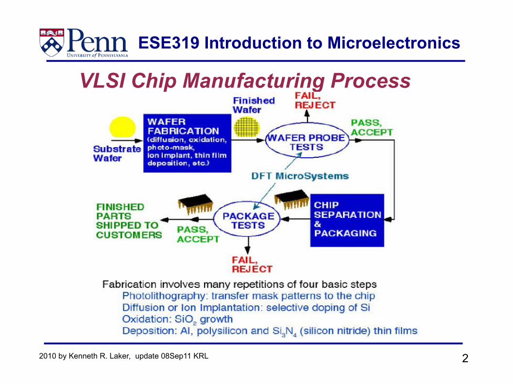
VLSI Chip Manufacturing Process
ESE319 Introduction to Microelectronics
32010 by Kenneth R. Laker, update 08Sep11 KRL
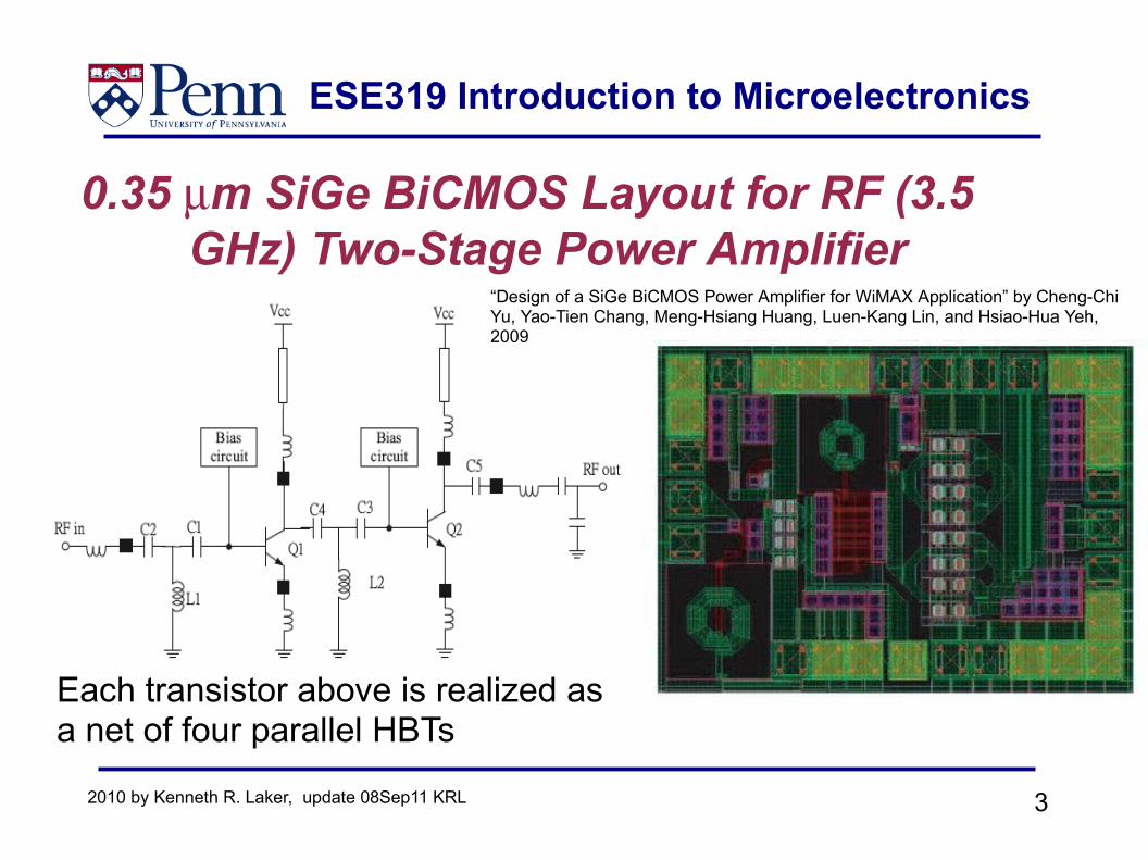
0.35 µm SiGe BiCMOS Layout for RF (3.5 GHz) Two-Stage Power Amplifier
Each transistor above is realized as a net of four parallel HBTs
“Design of a SiGe BiCMOS Power Amplifier for WiMAX Application” by Cheng-Chi Yu, Yao-Tien Chang, Meng-Hsiang Huang, Luen-Kang Lin, and Hsiao-Hua Yeh, 2009

ESE319 Introduction to Microelectronics
42010 by Kenneth R. Laker, update 08Sep11 KRL
Why BJT?What's the competition to BJT and bipolar technologies?
What advantages does the competition have over BJT?
What advantages does BJT and bipolar technologies have over their competition?
What circuit applications benefit from BJT and bipolar techno-logies?

ESE319 Introduction to Microelectronics
52010 by Kenneth R. Laker, update 08Sep11 KRL
Why BJTWhat's the competition to BJT and bipolar technologies?
MOSFET, in particular CMOS is the leading competitor
What advantages does the competition have over BJT?Small size (die area), low cost and low power dissipation
What advantages does BJT and bipolar technologies have over their competition?
High frequency operation, low noise, high current drive, high reliability in severe environmental conditions.
What circuit applications benefit from BJT & bipolar technolo-gies?
RF analog & digital circuits, power electronics, wireless communications, automobile electronics, rad hard electronics.
ESE319 Introduction to Microelectronics
62010 by Kenneth R. Laker, update 08Sep11 KRL
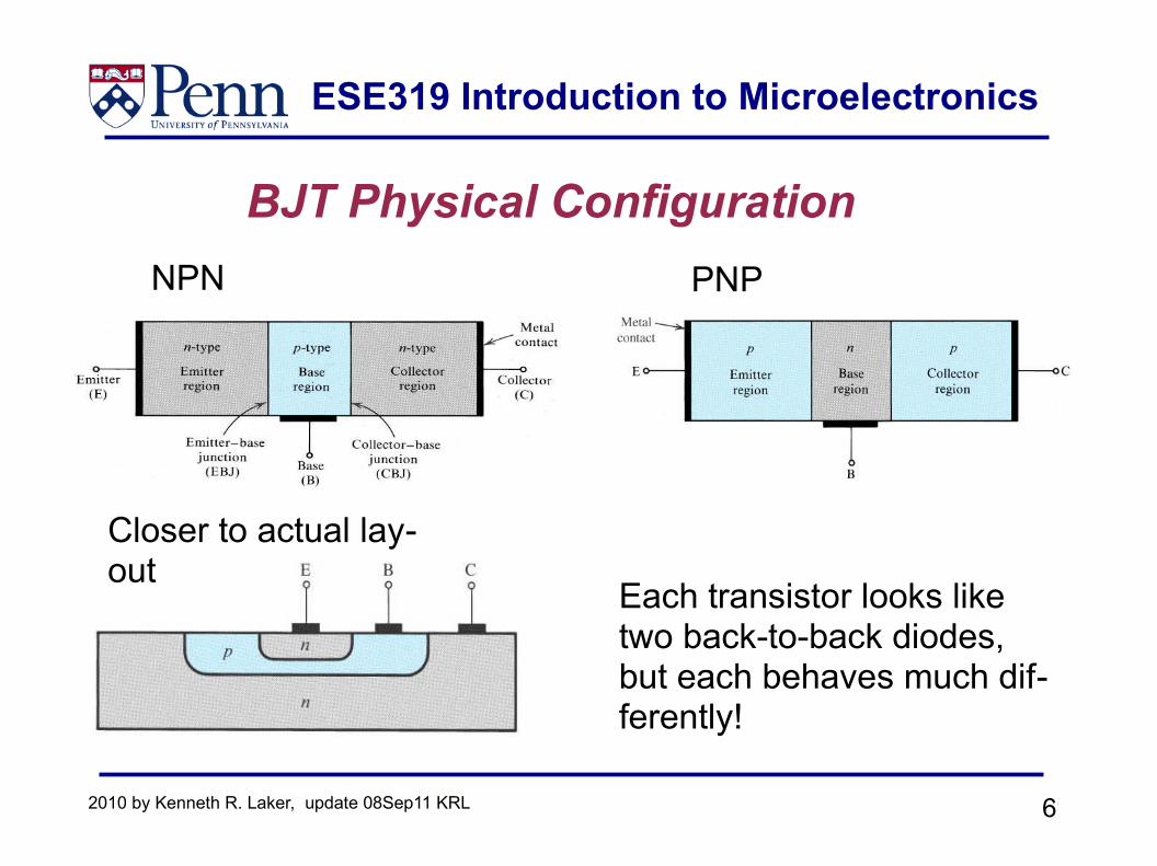
BJT Physical Configuration
Each transistor looks like two back-to-back diodes, but each behaves much dif-ferently!
NPN PNP
Closer to actual lay-out
ESE319 Introduction to Microelectronics
72010 by Kenneth R. Laker, update 08Sep11 KRL
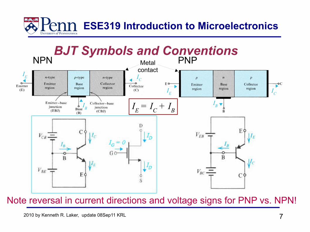
BJT Symbols and ConventionsNPN PNP
Note reversal in current directions and voltage signs for PNP vs. NPN!
IE
IE
Metal contactIC
IB
IC
IBIE = IC + IB
ESE319 Introduction to Microelectronics
82010 by Kenneth R. Laker, update 08Sep11 KRL
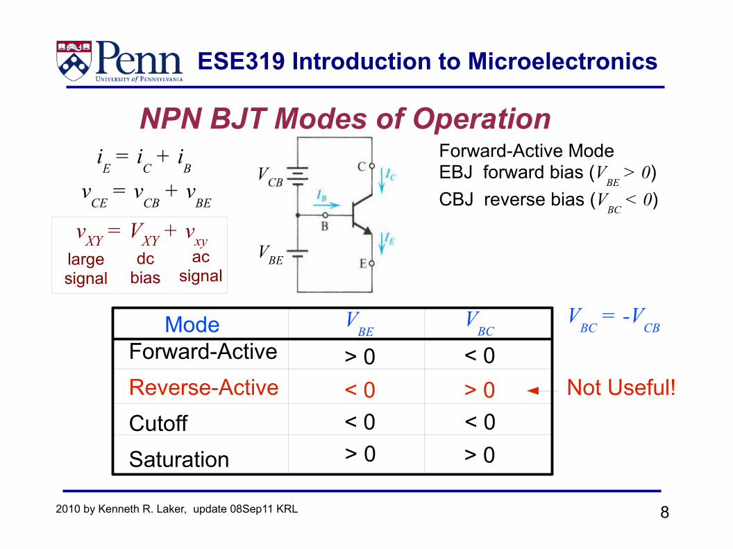
NPN BJT Modes of Operation
ModeForward-ActiveReverse-ActiveCutoffSaturation
VBE
VBC
> 0 < 0< 0 > 0< 0 < 0> 0 > 0
Forward-Active ModeEBJ forward bias (V
BE > 0)
CBJ reverse bias (VBC
< 0)
Not Useful!
VBC
= -VCB
vCE
= vCB
+ vBE
iE = i
C + i
B
VBE
VCB
vXY = VXY + vxylarge signal
dc bias
ac signal
ESE319 Introduction to Microelectronics
92010 by Kenneth R. Laker, update 08Sep11 KRL
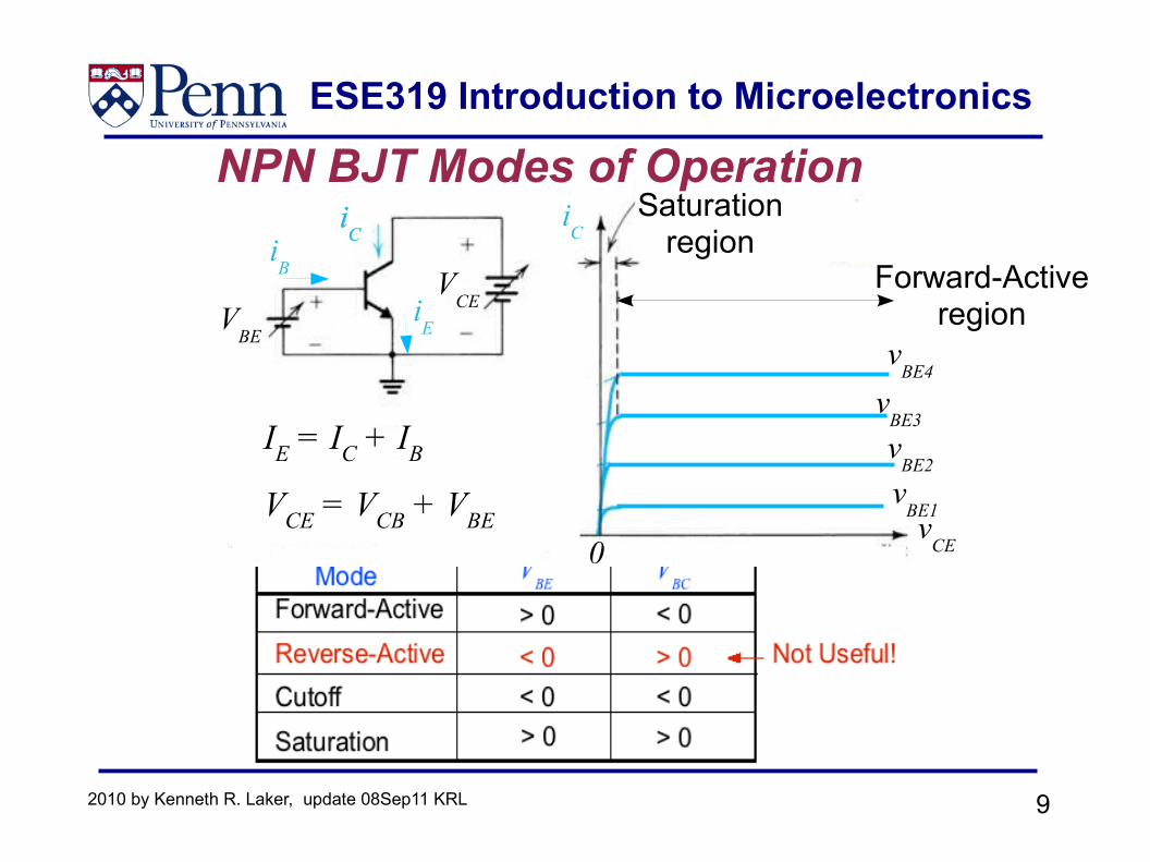
VBE
VCE
iC
iC
vCE
Saturation region
NPN BJT Modes of Operation
0
-VA
vBE1
vBE2
vBE3
vBE4
Forward-Active region
IE = IC + IB
VCE = VCB + VBE
iB
iE
iC
ESE319 Introduction to Microelectronics
102010 by Kenneth R. Laker, update 08Sep11 KRL
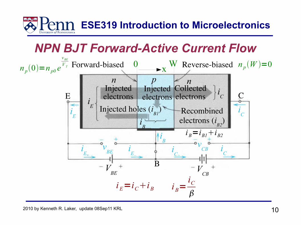
iE
iE
iE i
CiC
iC
iB v
CBvBE
VBE V
CB
iCi
E
n n
Recombined electrons (i
B2)i
B
p
Injected holes (iB1
)
Collected electrons
Injected electrons
Injected electrons
Forward-biased Reverse-biased
B
CE
NPN BJT Forward-Active Current Flow
i B=iB1iB2
iE=iCiB iB=iC
0 Wn p0=n p0 evBE
V T n p W =0x
ESE319 Introduction to Microelectronics
112010 by Kenneth R. Laker, update 08Sep11 KRL
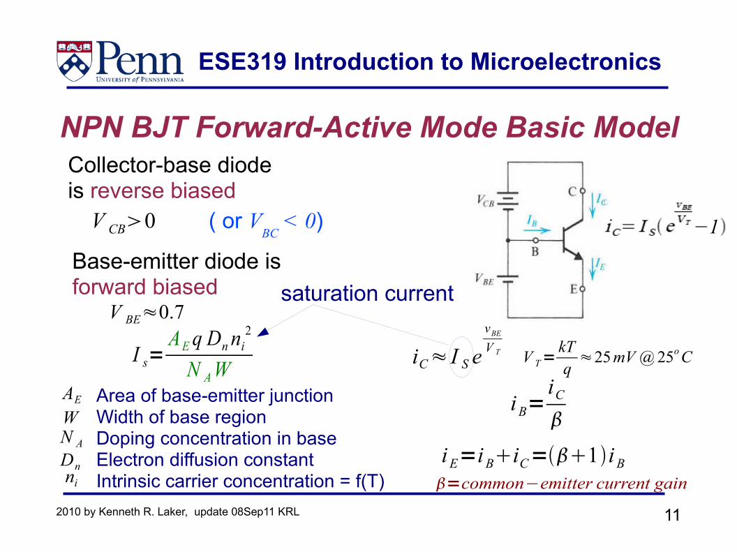
NPN BJT Forward-Active Mode Basic ModelCollector-base diode is reverse biased
V CB0
Base-emitter diode is forward biased
V BE≈0.7
iC≈ I S evBE
V T
iB=iC
iE=iBiC=1iB
V T=kTq≈25mV @ 25o CI s=
AE q Dn ni2
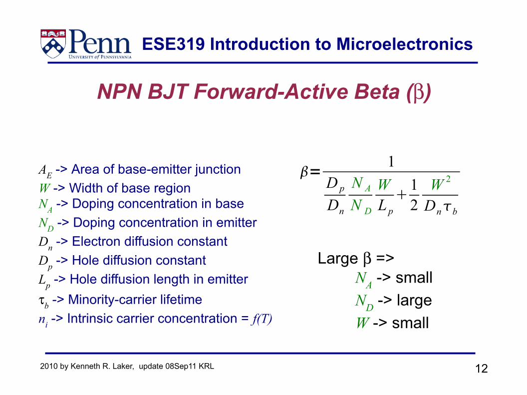
N A WArea of base-emitter junctionWidth of base regionDoping concentration in baseElectron diffusion constant Intrinsic carrier concentration = f(T) =common−emitter current gain
( or VBC
< 0)
saturation current
AE
WN A
ni
Dn
1
ESE319 Introduction to Microelectronics
122010 by Kenneth R. Laker, update 08Sep11 KRL
=1
D p
Dn
N A
N D
WL p
12
W 2
Dnb
AE -> Area of base-emitter junctionW -> Width of base regionNA -> Doping concentration in baseND -> Doping concentration in emitterDn -> Electron diffusion constant Dp -> Hole diffusion constant Lp -> Hole diffusion length in emitterτb -> Minority-carrier lifetimeni -> Intrinsic carrier concentration = f(T)
Large β =>NA -> smallND -> largeW -> small
NPN BJT Forward-Active Beta (β)
ESE319 Introduction to Microelectronics
132010 by Kenneth R. Laker, update 08Sep11 KRL
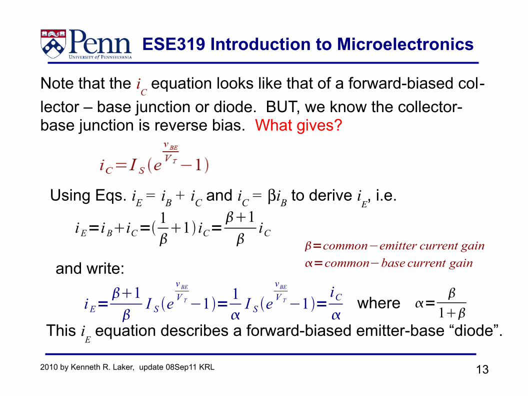
Note that the iC equation looks like that of a forward-biased col-
lector – base junction or diode. BUT, we know the collector-base junction is reverse bias. What gives?
Using Eqs. iE = iB + iC and iC = βiB to derive iE, i.e.
iE=iBiC=11 iC=
1
iC
and write:
iE=1
I S ev BE
V T −1= 1
I S evBE
V T −1=iC
This i
E equation describes a forward-biased emitter-base “diode”.
=common−emitter current gain=common−base current gain
=1
where
ESE319 Introduction to Microelectronics
142010 by Kenneth R. Laker, update 08Sep11 KRL
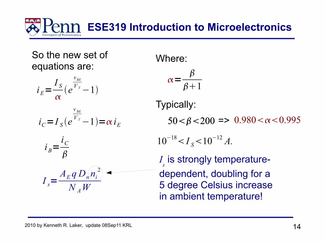
So the new set ofequations are:
iC=I S ev BE
V T −1= iE
iE=I S
e
vBE
V T −1
iB=iC
=
1
Where:
50200
10−18 I S10−12 A.
Typically:
Is is strongly temperature-
dependent, doubling for a 5 degree Celsius increase in ambient temperature!
50200
I s=AE q Dn ni
2
N A W
0.9800.995=>
ESE319 Introduction to Microelectronics
152010 by Kenneth R. Laker, update 08Sep11 KRL
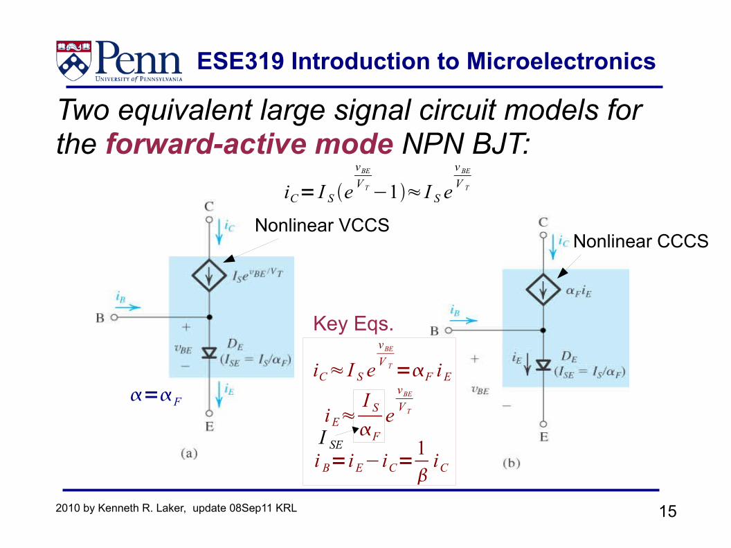
Two equivalent large signal circuit models for the forward-active mode NPN BJT:
Nonlinear VCCSNonlinear CCCS
iC≈ I S evBE
V T =F iE
iE≈I S
Fe
vBE
V T
Key Eqs.
=F
iC= I S evBE
V T −1≈ I S ev BE
V T
I SEi B=iE−iC=
1
iC
ESE319 Introduction to Microelectronics
162010 by Kenneth R. Laker, update 08Sep11 KRL
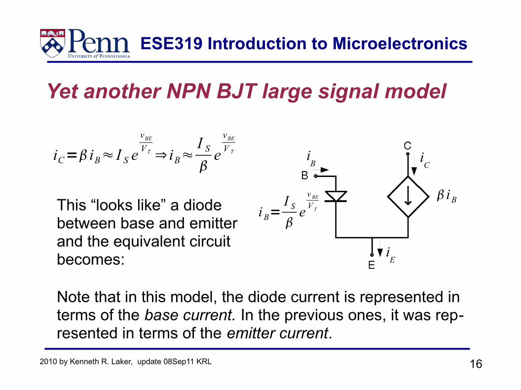
Yet another NPN BJT large signal model
iC= iB≈ I S evBE
V T ⇒ iB≈I S
e
vBE
V T
This “looks like” a diode between base and emitter and the equivalent circuit becomes:
Note that in this model, the diode current is represented in terms of the base current. In the previous ones, it was rep-resented in terms of the emitter current.
iB i
C
iE
iBi B=
I S
e
v BE
V T
ESE319 Introduction to Microelectronics
172010 by Kenneth R. Laker, update 08Sep11 KRL
NPN BJT Operating in the Reverse-Active Mode
● Weak transistor action if we:● Forward bias the base-collector junction and● Reverse bias the base-emitter junction● Collector and emitter reverse roles
● The physical construction of the transistor results ● Weak reverse-active performance
● Small values of β on the order of 0.01 to 1 ● Correspondingly smaller values of α, e. g.
R=R
R1≈0.11.1
≈0.091 for R=0.1
Recall for NPN Reverse-Active Mode VBE
< 0 & VBC
> 0
ESE319 Introduction to Microelectronics
182010 by Kenneth R. Laker, update 08Sep11 KRL
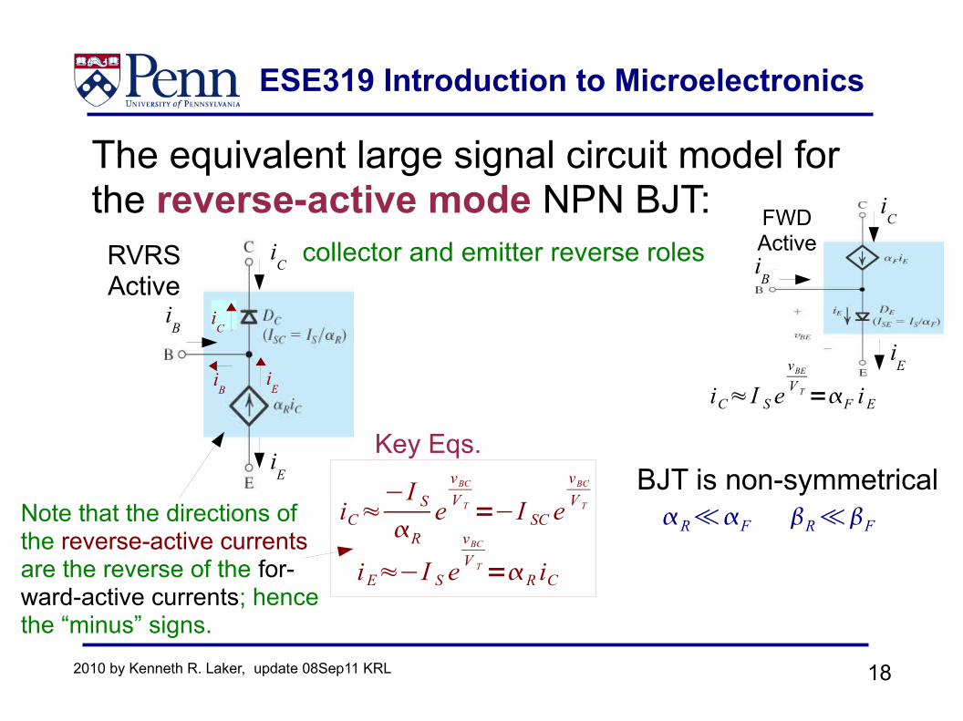
The equivalent large signal circuit model for the reverse-active mode NPN BJT:
iC≈−I S
Re
vBC
V T =−I SC evBC
V T
iE≈−I S evBC
V T =R iC
iB
iC
iE
RVRS Active
FWD Active
Key Eqs.BJT is non-symmetricalR≪F R≪FNote that the directions of
the reverse-active currents are the reverse of the for-ward-active currents; hence the “minus” signs.
iC
iEi
B
collector and emitter reverse roles
iC≈ I S evBE
V T =F iE
iB
iC
iE
ESE319 Introduction to Microelectronics
192010 by Kenneth R. Laker, update 08Sep11 KRL
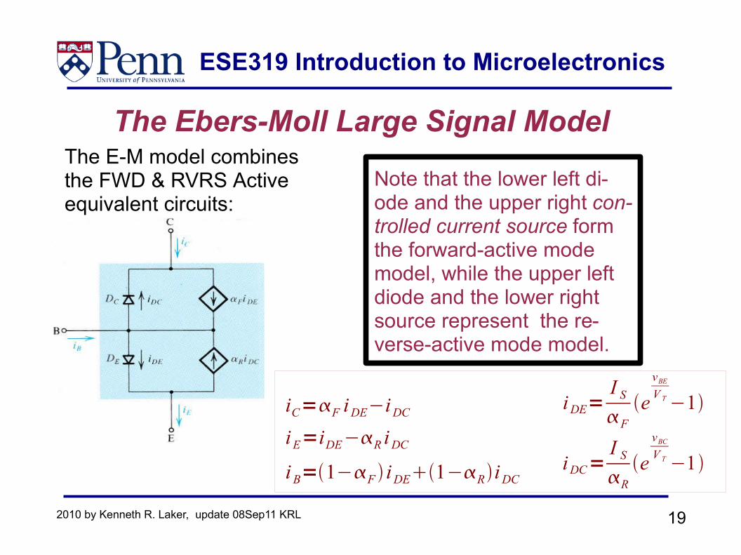
The Ebers-Moll Large Signal ModelThe E-M model combines the FWD & RVRS Active equivalent circuits:
Note that the lower left di-ode and the upper right con-trolled current source form the forward-active mode model, while the upper left diode and the lower right source represent the re-verse-active mode model.
iC=F iDE−i DC
iE=iDE−R i DC
i B=1−F iDE1−RiDC
i DE=I S
Fe
vBE
V T −1
iDC=I S
Re
vBC
V T −1
ESE319 Introduction to Microelectronics
202010 by Kenneth R. Laker, update 08Sep11 KRL
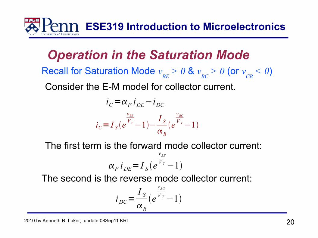
Operation in the Saturation Mode
Consider the E-M model for collector current. iC=F iDE−iDC
The first term is the forward mode collector current:
F iDE= I S evBE
V T −1The second is the reverse mode collector current:
iDC=I S
Re
vBC
V T −1
Recall for Saturation Mode vBE
> 0 & vBC
> 0 (or vCB
< 0)
iC= I S evBE
V T −1−I S
Re
v BC
V T −1
ESE319 Introduction to Microelectronics
212010 by Kenneth R. Laker, update 08Sep11 KRL
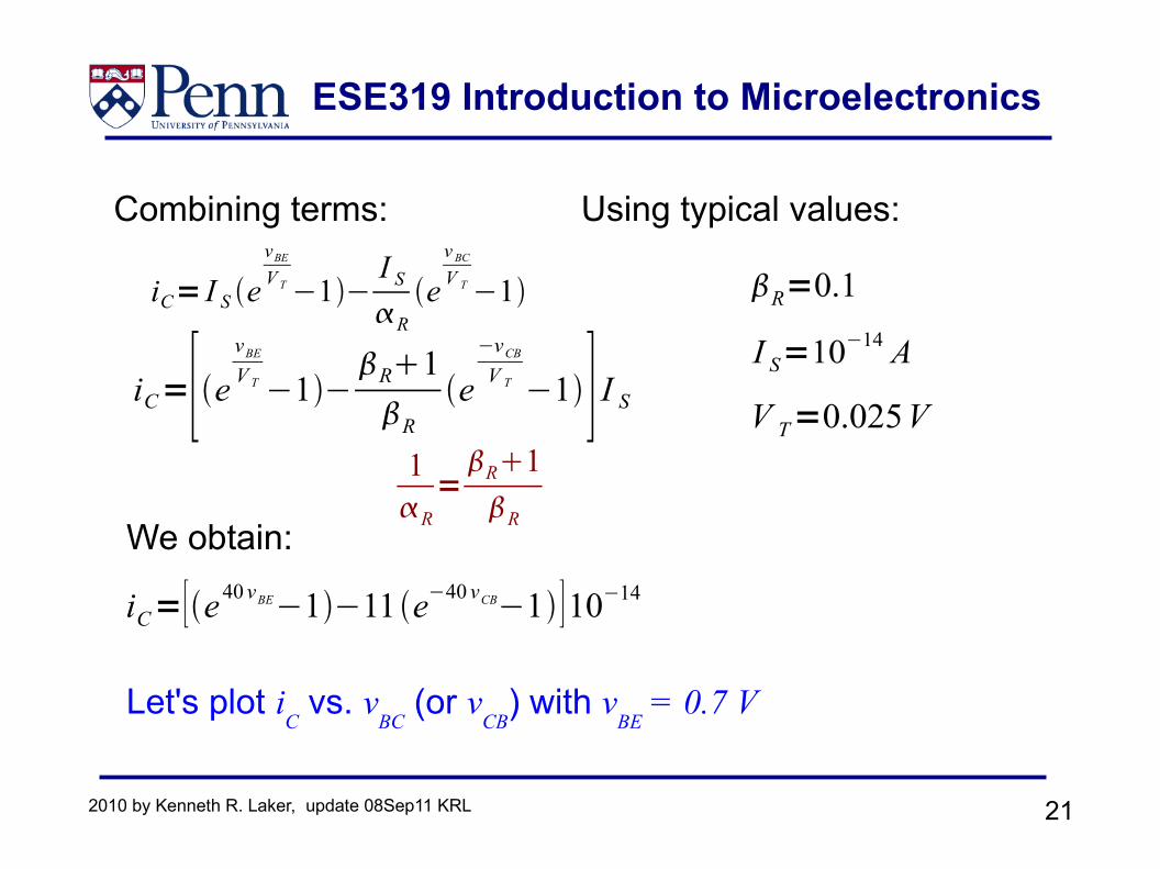
Combining terms:
iC=[e vBE
V T −1−R1R
e−vCB
V T −1] I S
Using typical values:
R=0.1
I S=10−14 A
V T=0.025V
iC=[e40 vBE−1−11 e−40 vCB−1 ]10−14We obtain:
1R
=R1R
iC= I S evBE
V T −1−I S
Re
v BC
V T −1
Let's plot iC vs. v
BC (or v
CB) with v
BE = 0.7 V
ESE319 Introduction to Microelectronics
222010 by Kenneth R. Laker, update 08Sep11 KRL
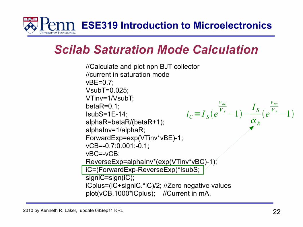
Scilab Saturation Mode Calculation//Calculate and plot npn BJT collector//current in saturation modevBE=0.7;VsubT=0.025;VTinv=1/VsubT;betaR=0.1;IsubS=1E-14;alphaR=betaR/(betaR+1);alphaInv=1/alphaR;ForwardExp=exp(VTinv*vBE)-1;vCB=-0.7:0.001:-0.1;vBC=-vCB;ReverseExp=alphaInv*(exp(VTinv*vBC)-1);iC=(ForwardExp-ReverseExp)*IsubS;signiC=sign(iC);iCplus=(iC+signiC.*iC)/2; //Zero negative valuesplot(vCB,1000*iCplus); //Current in mA.
iC=I S ev BE
V T −1−I S
Re
vBC
V T −1
ESE319 Introduction to Microelectronics
232010 by Kenneth R. Laker, update 08Sep11 KRL
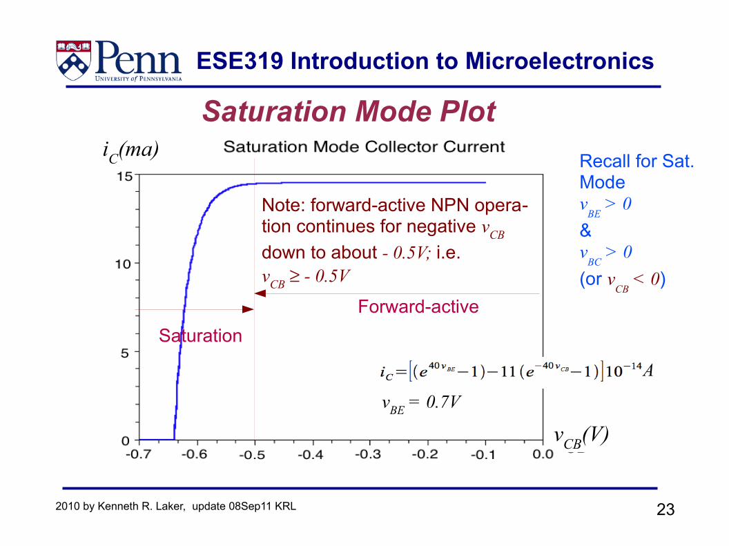
Saturation Mode Plot
Forward-activeSaturation
Recall for Sat. Mode v
BE > 0
& v
BC > 0
(or vCB
< 0)
A
iC(ma)
vCB(V)vBE = 0.7V
Note: forward-active NPN opera-tion continues for negative vCB down to about - 0.5V; i.e. vCB ≥ - 0.5V
ESE319 Introduction to Microelectronics
242010 by Kenneth R. Laker, update 08Sep11 KRL
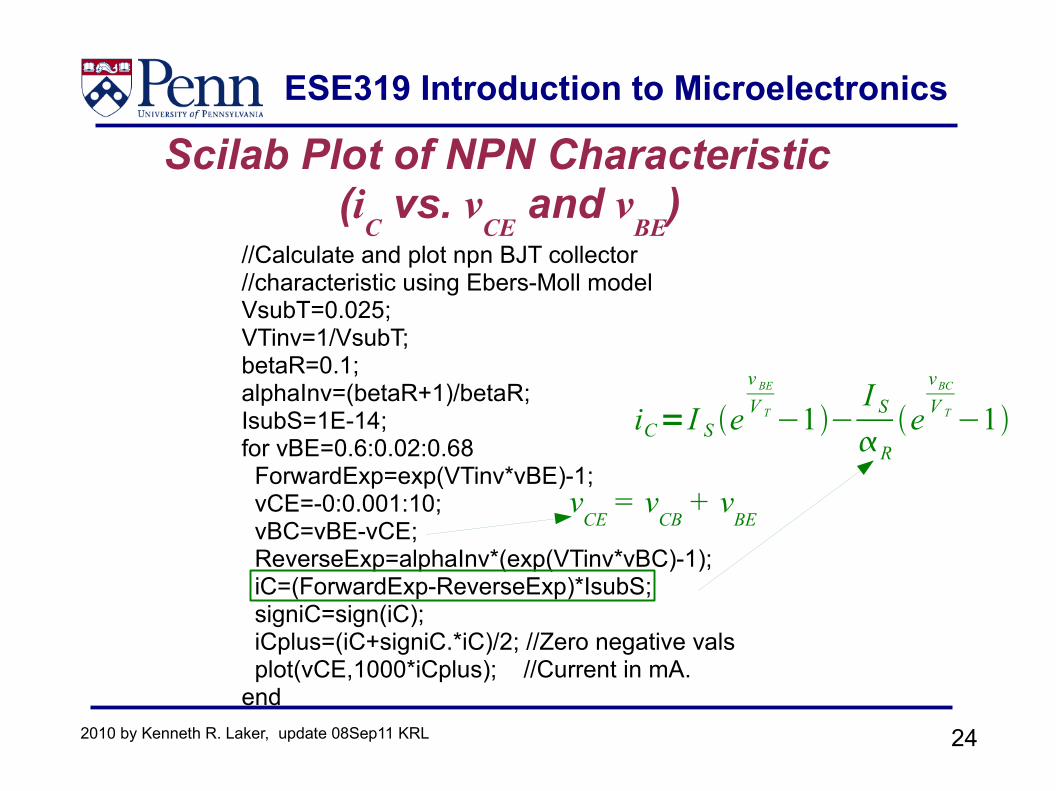
Scilab Plot of NPN Characteristic (iC vs. v
CE and v
BE)
//Calculate and plot npn BJT collector//characteristic using Ebers-Moll modelVsubT=0.025;VTinv=1/VsubT;betaR=0.1;alphaInv=(betaR+1)/betaR;IsubS=1E-14;for vBE=0.6:0.02:0.68 ForwardExp=exp(VTinv*vBE)-1; vCE=-0:0.001:10; vBC=vBE-vCE; ReverseExp=alphaInv*(exp(VTinv*vBC)-1); iC=(ForwardExp-ReverseExp)*IsubS; signiC=sign(iC); iCplus=(iC+signiC.*iC)/2; //Zero negative vals plot(vCE,1000*iCplus); //Current in mA.end
iC=I S ev BE
V T −1−I S
Re
vBC
V T −1
vCE
= vCB
+ vBE
ESE319 Introduction to Microelectronics
252010 by Kenneth R. Laker, update 08Sep11 KRL
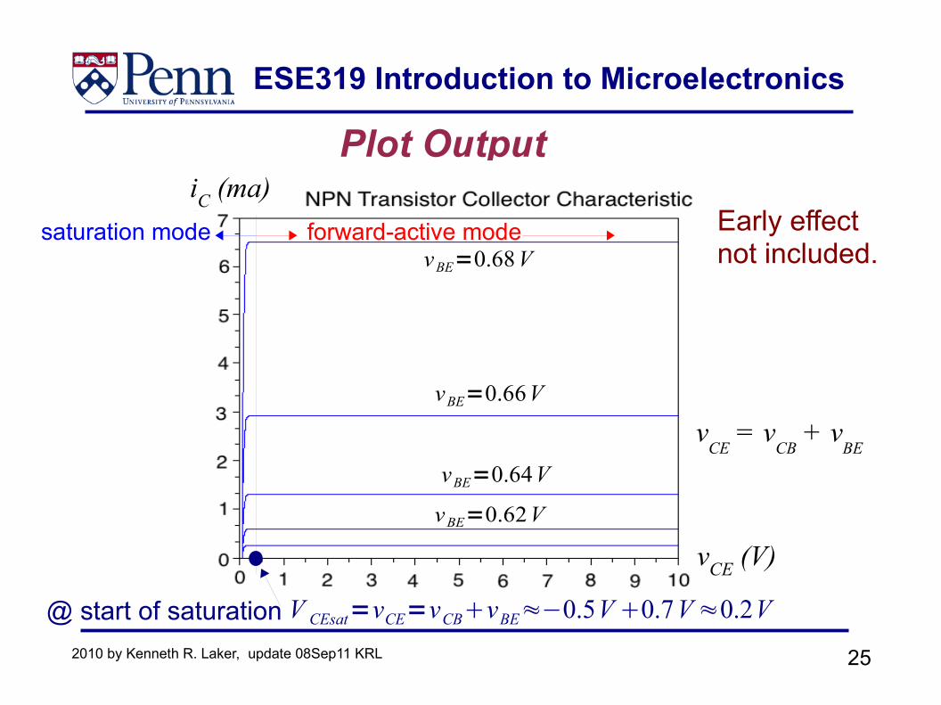
Plot Output
vBE=0.68V
vBE=0.66V
vBE=0.64V
Early effect not included.
forward-active modesaturation mode
vCE (V)
iC (ma)
vCE
= vCB
+ vBE
vBE=0.62V
V CEsat=vCE=vCBvBE≈−0.5V 0.7V≈0.2V@ start of saturation
ESE319 Introduction to Microelectronics
262010 by Kenneth R. Laker, update 08Sep11 KRL
More on NPN Saturation● The base-collector diode has much larger
area than the base-emitter one.● Therefore, with the same applied voltage, it will
conduct a much larger forward current than will the base-emitter diode.
● When the collector-emitter voltage drops below the base-emitter voltage, the base-collector di-ode is forward biased and conducts heavily.
vCE≈V CEsat=vCBvBE≈0.2V¿0.3V ¿
vCB=vCE−vBE =>
iC= I S evBE
V T −1−I S
Re
v BC
V T −1 where αR << 1
ESE319 Introduction to Microelectronics
272010 by Kenneth R. Laker, update 08Sep11 KRL
More on NPN Saturation - cont.● In saturation the forward-biased current through
the collector-base junction increases iB and de-
creases iC as v
BC increases.
● Test for saturation mode operation● v
CE = V
CEsat = 0.1 to 0.3 V => collector-base junction is
forward biased
● Current ratio => collector-base junction is forward biased
iC
iB
sat≤
or
sat= forced=iC
iB
sat≤
ESE319 Introduction to Microelectronics
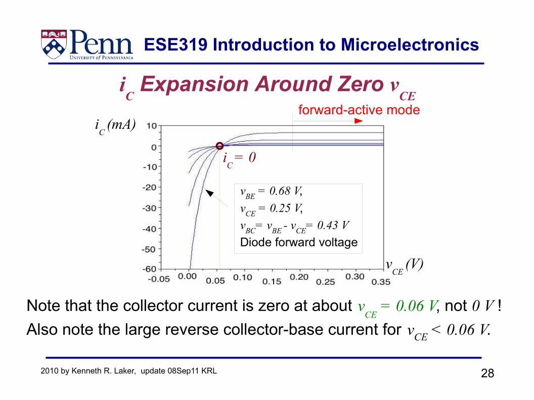
282010 by Kenneth R. Laker, update 08Sep11 KRL
iC Expansion Around Zero v
CE
Note that the collector current is zero at about vCE
= 0.06 V, not 0 V ! Also note the large reverse collector-base current for vCE < 0.06 V.
iC
(mA)
vCE
(V)
iC
= 0
vBE = 0.68 V,vCE = 0.25 V,vBC= vBE - vCE= 0.43 VDiode forward voltage
forward-active mode
ESE319 Introduction to Microelectronics
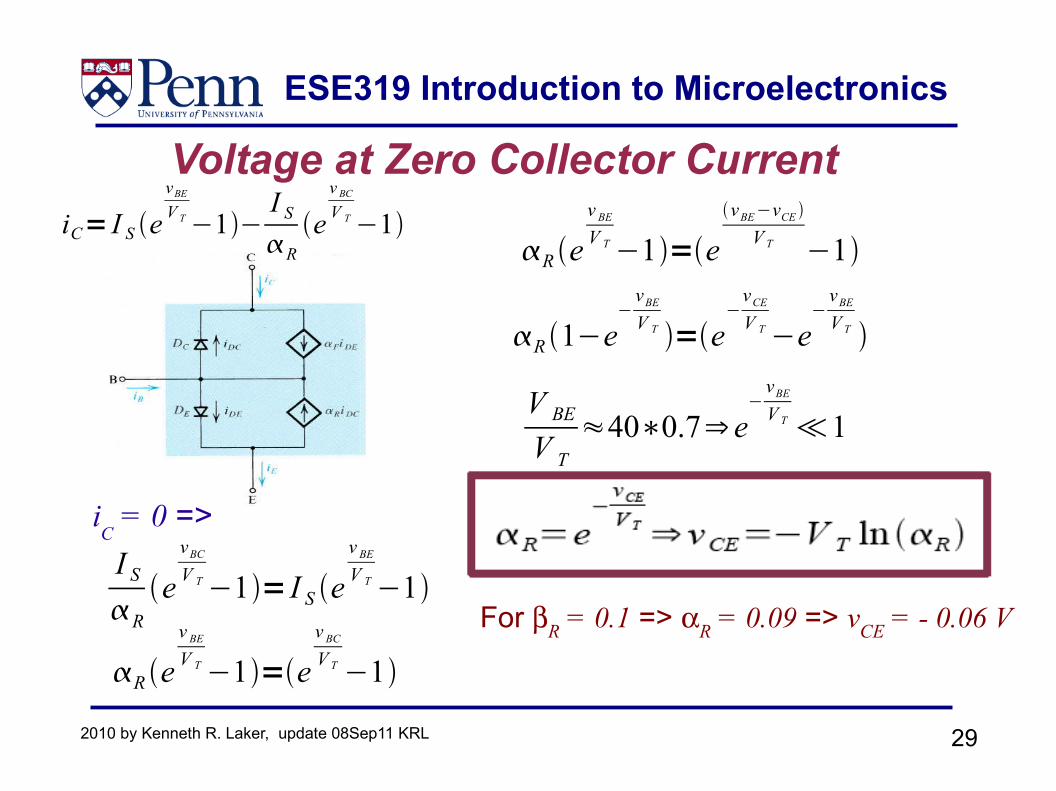
292010 by Kenneth R. Laker, update 08Sep11 KRL
Voltage at Zero Collector Current
iC = 0 =>I S
Re
vBC
V T −1= I S ev BE
V T −1
R ev BE
V T −1=ev BC
V T −1
R ev BE
V T −1=evBE−vCE
V T −1
R 1−e−
vBE
V T =e−
vCE
V T −e−
vBE
V T
V BE
V T≈40∗0.7⇒ e
−vBE
V T ≪1
iC= I S evBE
V T −1−I S
Re
v BC
V T −1
For βR = 0.1 => αR = 0.09 => vCE = - 0.06 V
ESE319 Introduction to Microelectronics
302010 by Kenneth R. Laker, update 08Sep11 KRL
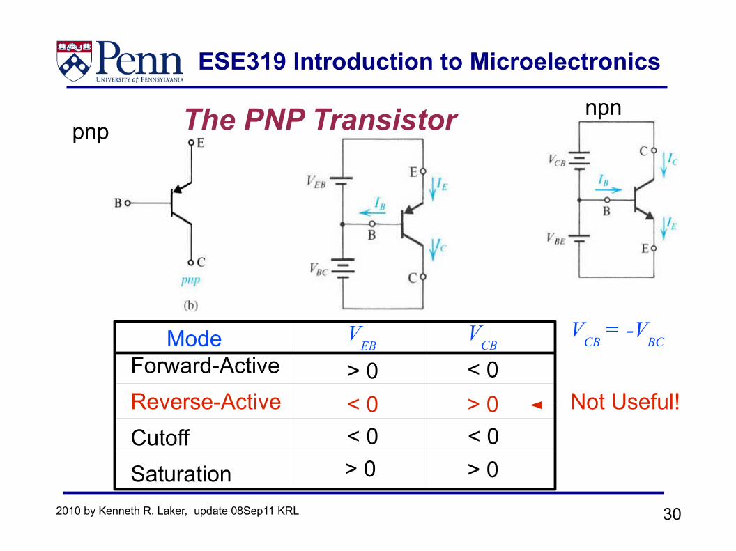
The PNP Transistor npnpnp
ModeForward-ActiveReverse-ActiveCutoffSaturation
VEB
VCB
> 0 < 0< 0 > 0< 0 < 0
> 0
Not Useful!
VCB
= -VBC
> 0
ESE319 Introduction to Microelectronics
312010 by Kenneth R. Laker, update 08Sep11 KRL
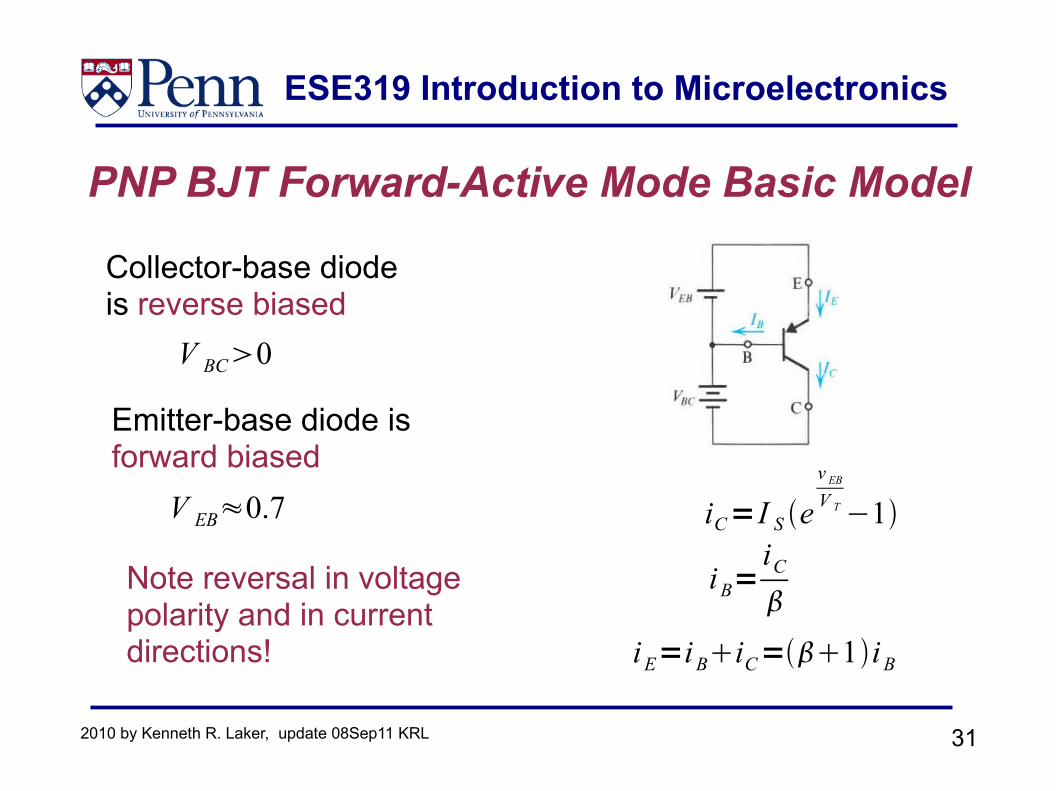
PNP BJT Forward-Active Mode Basic Model
Collector-base diode is reverse biased
V BC0
Emitter-base diode is forward biased
V EB≈0.7 iC=I S ev EB
V T −1
iB=iC
iE=iBiC=1iB
Note reversal in voltage polarity and in current directions!
ESE319 Introduction to Microelectronics
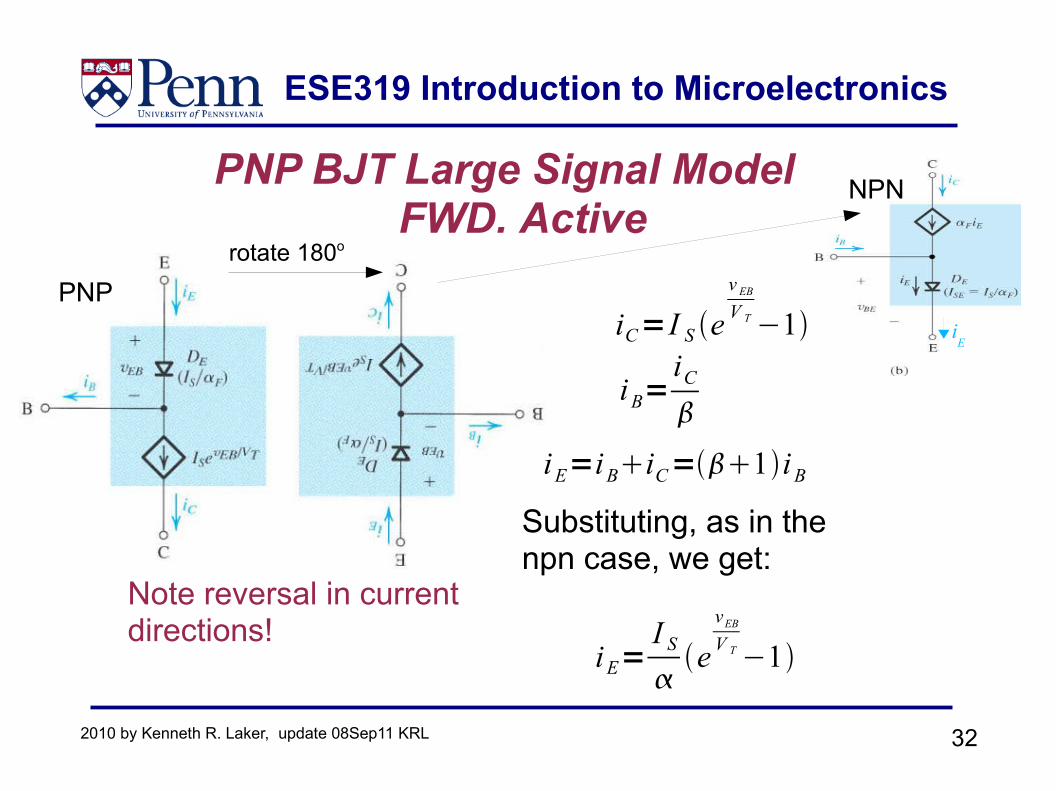
322010 by Kenneth R. Laker, update 08Sep11 KRL
PNP BJT Large Signal Model FWD. Active
Note reversal in current directions!
iC=I S ev EB
V T −1
iB=iC
iE=I S
e
vEB
V T −1
NPN
Substituting, as in the npn case, we get:
iE=iBiC=1iB
rotate 180o
iE
PNP
ESE319 Introduction to Microelectronics
332010 by Kenneth R. Laker, update 08Sep11 KRL
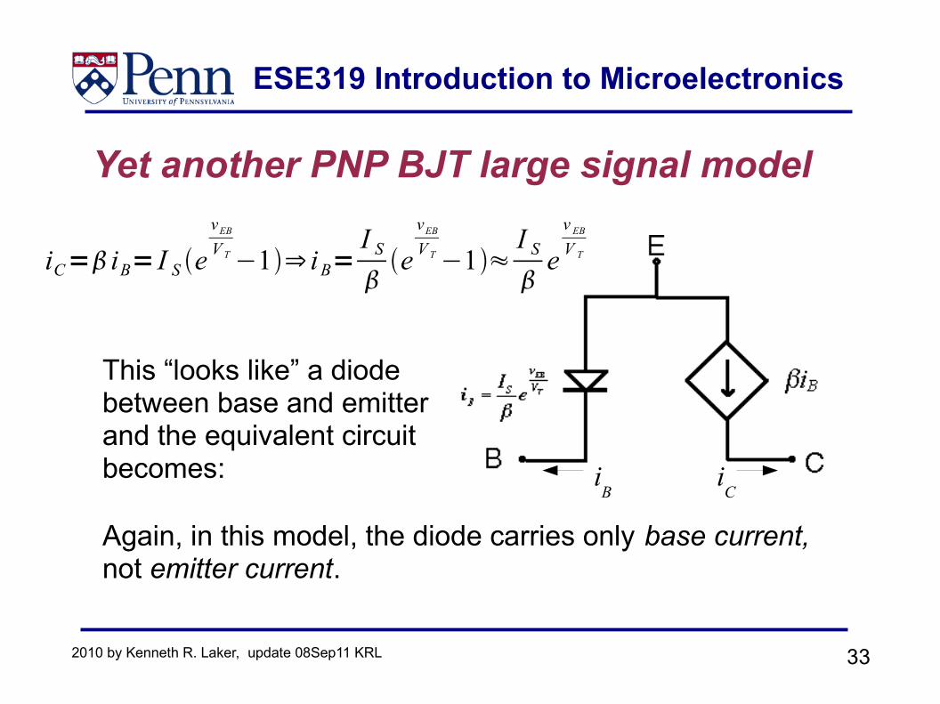
Yet another PNP BJT large signal model
This “looks like” a diode between base and emitter and the equivalent circuit becomes:
Again, in this model, the diode carries only base current, not emitter current.
iB
iC
iC= iB= I S evEB
V T −1⇒ iB=I S
e
vEB
V T −1≈I S
e
v EB
V T