Embed Size (px)
Citation preview

EE 434Lecture 24
Bipolar Small Signal Device Models

Quiz 16What is a “binning model” and what is the purpose of using “binning models”?

And the number is ….
631
24578
9

And the number is ….
631
24578
9

Quiz 16What is a “binning model” and what is the purpose of using “binning models”?
Solution:
A binning model is actually a set of models whereby the model derived for dimensions close to those of a specific device is used rather than using the same model for each device (the functional form of most binning models does not change, simply the parameters in the model)
A good binning model will more closely predict the actual characteristics of a device than a model that does not change with device dimensions.

Models for Computer Simulation
Simple dc Model
Small SignalModel
Frequency-Dependent Small Signal Model
Better Analytical dc Models
Sophisticated Model for Computer Simulations
Better Modelsfor Predicting
Device Operation
Review from Last Time
Concept in modeling is to partition model into two parts, one that characterizes the technology and the other that characterizes the geometric aspects of a device
Technology part of the model common to all devices in a process(Level 1, BSIM4 , PSP models – over 100 paramaters in BSIM 4 model)
Geometric information unique to each device{W,L,NRD, NRS, AD,AS,PD,PS}, (default values used in not specified)
Models based upon physical principles but emperically modified to either simplfy model or improve validity
Geometric description may not be unique
Anticipated parasitics often included at schematic level for design prior to layout
Hierarchy used in models
Review from Last Time

Bipolar Models
Simple dc Model
Small SignalModel
Frequency-Dependent Small Signal Model
Better Analytical dc Models
Sophisticated Model for Computer Simulations
Better Modelsfor Predicting
Device Operation
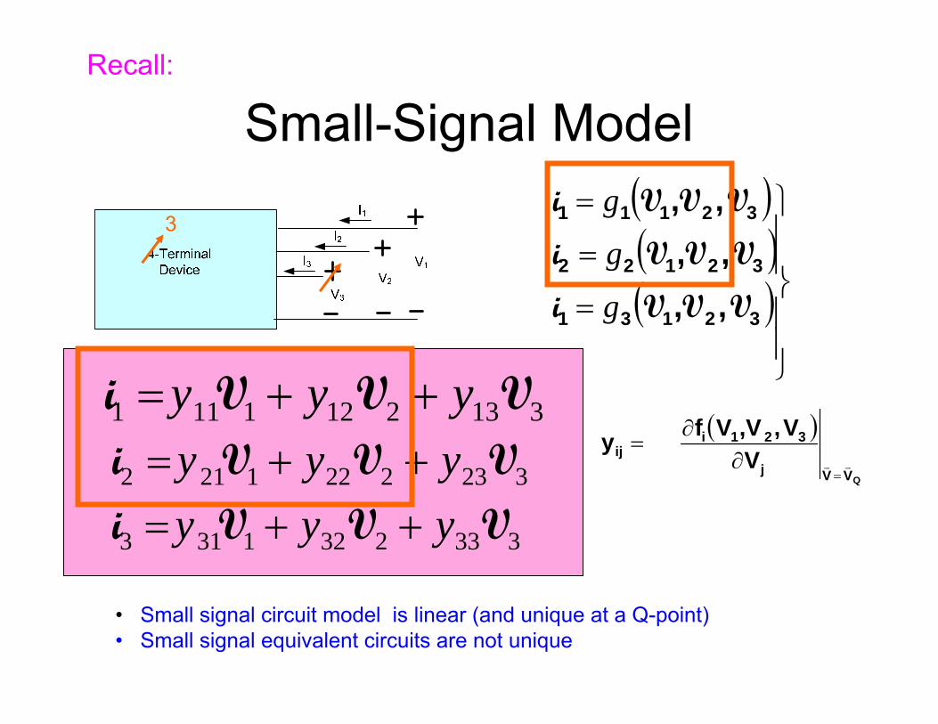
Small-Signal Model( )( )( )
⎪⎪
⎭
⎪⎪
⎬
⎫
=
=
=
32131
32122
32111
,,,,,,
VVVi
VVVi
VVVi
g
g
g
3232221212 Vyyy ++= VVi
3332321313 Vyyy ++= VVi
3132121111 Vyyy ++= VVi( )
QVVj
321iij V
V,,VVfy=
∂∂
=
• Small signal circuit model is linear (and unique at a Q-point)• Small signal equivalent circuits are not unique
Recall:

Small-Signal Model( )( )( )
⎪⎪
⎭
⎪⎪
⎬
⎫
=
=
=
32131
32122
32111
,,,,,,
VVVi
VVVi
VVVi
g
g
g
Small signal model is that which represents the relationship between the small signal voltages and the small signal currents
For small signals, this relationship should be linear
Recall:
Small-Signal Model( )( )( )
⎪⎪
⎭
⎪⎪
⎬
⎫
=
=
=
32131
32122
32111
,,,,,,
VVVi
VVVi
VVVi
g
g
g
3232221212 Vyyy ++= VVi
3332321313 Vyyy ++= VVi
3132121111 Vyyy ++= VVi( )
QVVj
321iij V
V,,VVfy=
∂∂
=
• Small signal circuit model is linear (and unique at a Q-point)• Small signal equivalent circuits are not unique
Recall:
3
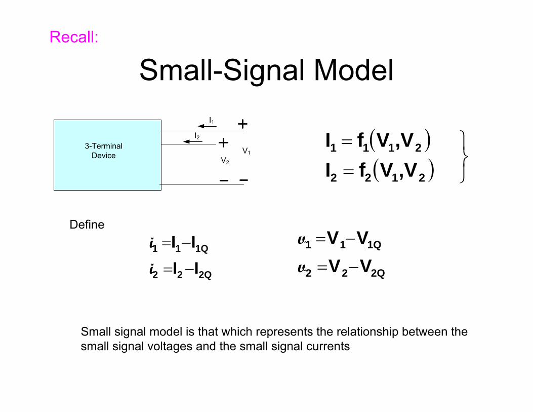
Small-Signal Model
( )( ) ⎭
⎬⎫
==
2122
2111
,VVfI,VVfI
I1
I2
V1V2
3-TerminalDevice
Define
2Q22
1Q11
IIII−=
−=
i
i
2Q22
1Q11
VVVV−=
−=
v
v
Small signal model is that which represents the relationship between the small signal voltages and the small signal currents
Recall:

Small-Signal Model
( )( ) ⎪⎭
⎪⎬⎫
=
=
2122
2111
,,VVi
VVi
g
g
I1I2
V1V2
3-TerminalDevice
2221212 VVi yy +=2121111 VVi yy +=
( )
QVVj
21iij V
,VVfy=
∂∂
=
Recall:
A Small Signal Equivalent Circuit
⎟⎟⎠
⎞⎜⎜⎝
⎛=
2Q
1Q
VV
V
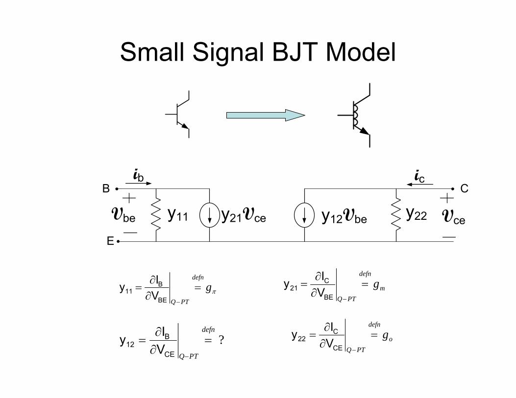
Small Signal BJT Model
B
E
C
Vbe
ic
12Vbe21Vce11 22 Vce
ib
πgdefn
PTQ
=∂∂
=−BE
B11 V
Iy
?defn
PTQ
=∂∂
=−CE
B12 V
Iy
m
defn
PTQ
g=∂∂
=−BE
C21 V
Iy
o
defn
PTQ
g=∂∂
=−CE
C22 V
Iy

Small Signal BJT Model
⎟⎟⎠
⎞⎜⎜⎝
⎛+=
AF
CEBC V
V1βII
πgdefn
PTQ
=∂∂
=−BE
B11 V
Iy
?defn
PTQ
=∂∂
=−CE
B12 V
Iy
m
defn
PTQ
g=∂∂
=−BE
C21 V
Iy
o
defn
PTQ
g=∂∂
=−CE
C22 V
Iy
Region of Operation for Small Signal Model : Forward Active
t
BE
VV
ESB e
βAJI =“1”
“2”t
CQVV
EStBE
C21 V
IeAJV1
VIy t
BE
=⎟⎟
⎠
⎞
⎜⎜
⎝
⎛=
∂∂
==− PTQPTQ
t
CQ
t
BQVV
ES
tBE
B11 βV
IVIeAJ
V1
VIy t
BE
==⎟⎟
⎠
⎞
⎜⎜
⎝
⎛=
∂∂
==− PTQPTQ β
0=∂∂
=−PTQCE
B12 V
Iy
AF
CQ
oPTQ
VV
ESAFCE
C22 V
IeAJV1
VIy t
BE
≅⎥⎥
⎦
⎤
⎢⎢
⎣
⎡=
∂∂
=−−PTQ
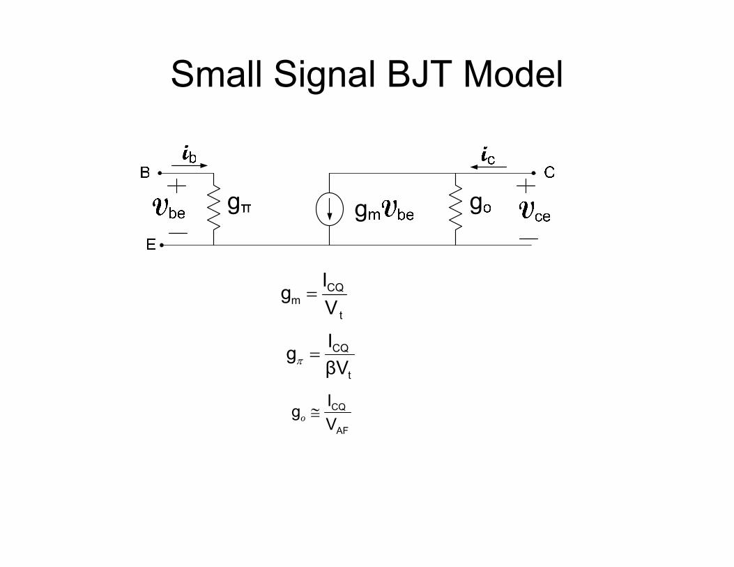
Small Signal BJT Model
t
CQm V
Ig =
t
CQ
βVIg =π
AF
CQ
VIg ≅o

Small Signal BJT Model
t
CQm V
Ig =t
CQ
βVIg =π
AF
CQ
VIg ≅o
bbe iv =πg
π
mm g
gg bbe iv =
β
βVIVI
gg
t
Q
t
Q
π
m =
⎥⎦
⎤⎢⎣
⎡
⎥⎦
⎤⎢⎣
⎡
=
bbe iv βgm =
Observe :

Small Signal BJT Model
t
CQm V
Ig =t
CQ
βVIg =π
AF
CQ
VIg ≅o
t
CQ
βVIg =π
AF
CQ
VIg ≅o
B
E
C
Vbe
ic
o Vce
ib
π biβ
Alternate equivalent small signal model
Properties of the BJT
• Alternate Equivalent Small Signal Model• Relative magnitude of small signal
parameters– Simplified small signal model

Small Signal BJT Model
t
CQm V
Ig =t
CQ
βVIg =π
AF
CQ
VIg ≅o
bbe iv =πg
π
mm g
gg bbe iv =
β
βVIVI
gg
t
Q
t
Q
π
m =
⎥⎦
⎤⎢⎣
⎡
⎥⎦
⎤⎢⎣
⎡
=
bbe iv βgm =
Observe :

Small Signal BJT Model
t
CQm V
Ig =t
CQ
βVIg =π
AF
CQ
VIg ≅o
t
CQ
βVIg =π
AF
CQ
VIg ≅o
B
E
C
Vbe
ic
o Vce
ib
π biβ
Alternate equivalent small signal model

Properties of the BJT
• Alternate Equivalent Small Signal Model• Magnitude of small signal parameters

Relative Magnitude of Small Signal Parameters
t
CQm V
Ig =t
CQ
βVIg =π
AF
CQ
VIg ≅o
β
βVIVI
gg
t
Q
t
Q
π
m =
⎥⎦
⎤⎢⎣
⎡
⎥⎦
⎤⎢⎣
⎡
=
7726mV100
200VVβ
V
VIVβ
I
gg
t
AF
AF
Q
t
Q
o
π =•
≈=
⎥⎦
⎤⎢⎣
⎡
⎥⎦
⎤⎢⎣
⎡
=
oπm ggg >>>>
Often the go term can be neglected in the small signal model because it is so small

Relative Magnitude of Small Signal Parameters
t
CQm V
Ig =t
CQ
βVIg =π
AF
CQ
VIg ≅o
β
βVIVI
gg
t
Q
t
Q
π
m =
⎥⎦
⎤⎢⎣
⎡
⎥⎦
⎤⎢⎣
⎡
=
7726mV100
200VVβ
V
VIVβ
I
gg
t
AF
AF
Q
t
Q
o
π =•
≈=
⎥⎦
⎤⎢⎣
⎡
⎥⎦
⎤⎢⎣
⎡
=
oπm ggg >>>>
Often the go term can be neglected in the small signal model because it is so small
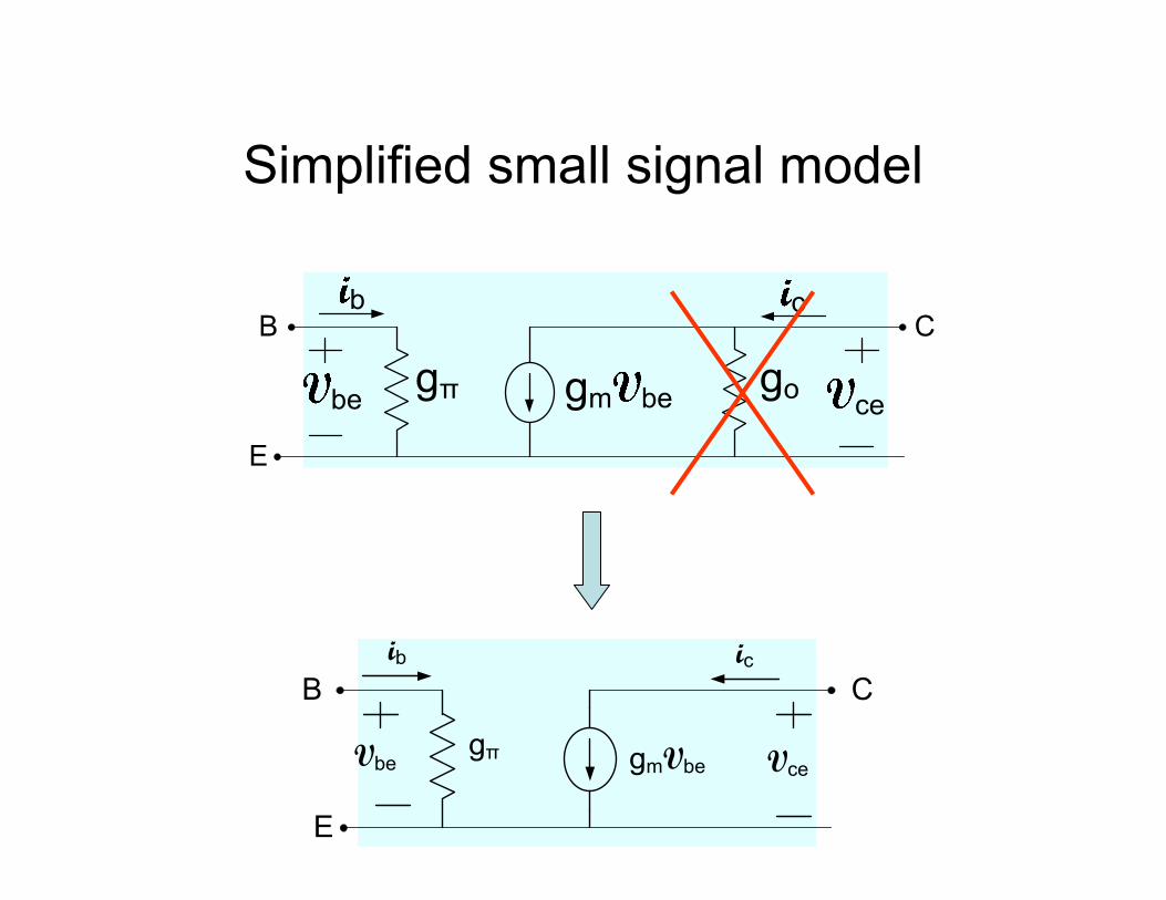
Simplified small signal model
Vbe
ic
mVbe Vce
ib
π

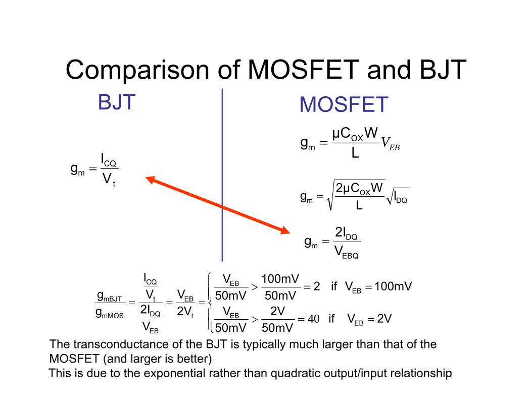
Comparison of BJT and MOSFET

Comparison of MOSFET and BJT
t
CQm V
Ig =
EBVL
WµCg OXm =
DQOX
m IL
WC2µg =
EBQ
DQm V
2Ig =
BJT MOSFET
⎪⎪⎩
⎪⎪⎨
⎧
==>
==>===
2VVif50mV
2V50mV
V
100mVV if250mV
100mV50mV
V
2VV
V2IVI
gg
EBEB
EBEB
t
EB
EB
DQ
t
CQ
mMOS
mBJT
40
The transconductance of the BJT is typically much larger than that of the MOSFET (and larger is better!) This is due to the exponential rather than quadratic output/input relationship
Comparison of MOSFET and BJT
t
CQm V
Ig =
EBVL
WµCg OXm =
DQOX
m IL
WC2µg =
EBQ
DQm V
2Ig =
BJT MOSFET
⎪⎪⎩
⎪⎪⎨
⎧
==>
==>===
2VVif50mV
2V50mV
V
100mVV if250mV
100mV50mV
V
2VV
V2IVI
gg
EBEB
EBEB
t
EB
EB
DQ
t
CQ
mMOS
mBJT
40
The transconductance of the BJT is typically much larger than that of the MOSFET (and larger is better)This is due to the exponential rather than quadratic output/input relationship

Comparison of MOSFET and BJT
AF
CQ
VIg ≅o DQIλ=og
BJT MOSFET
5.020001.
11 =≈== − VVAFDQ
AF
CQ
oMOS
oBJT
V1
IVI
gg
λλ
The output conductances are comparable but that of the BJT is usually modestly smaller (and smaller is better!)

Comparison of MOSFET and BJT
t
CQ
βVIg =π
BJT MOSFET
0=πg
gπ of a MOSFET is much smaller than that of a BJT (and smaller is better!)
gπ is the reciprocal of the input impedance

Comparison of MOSFET and BJTBJT MOSFET
Assume BJT operating in FA region, MOSFET operating in Saturation
Assume same quiescent output voltage and same resistor R1One of the most widely used amplifier architectures

Comparison of MOSFET and BJT
R1
Q1
VIN(t)
VOUT
VCC
VEE
BJT MOSFET
1
VIN
VOUT
1
VIN
VOUT

Comparison of MOSFET and BJTBJT MOSFET
1
VIN
VOUT
1
VIN
VOUT
assume go can be neglected assume go can be neglected
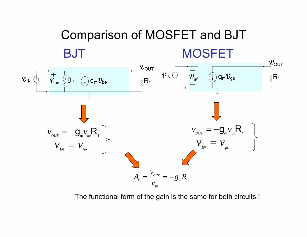
Comparison of MOSFET and BJTBJT MOSFET
m 1g R
OUT gsv v= −
IN gsv v=
m 1g R
OUT bev v= −
IN bev v=
1OUT
V m
IN
vA g Rv
= = −
The functional form of the gain is the same for both circuits !

Comparison of MOSFET and BJTBJT MOSFET
1OUT
V m
IN
vA g Rv
= = − 1OUT
V m
IN
vA g Rv
= = −
CQ 1VBJT
t
I RAV
= − DQ 1VMOS
EB
2I RAV
= −
For the same power level and the same quiescent voltage drop across R1, the BJT will generally have a much larger gain since usually Vt<<VEB

Comparison of MOSFET and BJTBJT MOSFET
Assume BJT operating in FA region, MOSFET operating in SaturationAssume same bias current
One of the most widely used amplifier architectures in integrated applications
Special Case of Previous Architecture

Comparison of MOSFET and BJTBJT MOSFET

Comparison of MOSFET and BJTBJT MOSFET
assume go can be neglected assume go can be neglected
OUTV
IN
vAv
= = −∞
• AV is unrealistically large• Must include more accurate small-signal model !

Comparison of MOSFET and BJTBJT MOSFET
include go effects include go effects
OUT mV
IN o
v gAv g
= = −
Functional form of gain is the same for both circuits

Comparison of MOSFET and BJTBJT MOSFET
OUT mV
IN o
v gAv g
= = −
• BJT Gain is Very Large and Independent of Operating Point• MOS Gain is dependent upon operating conditions (VEB)• VAF and 2/λ are comparable for large MOS devices, VAF considerably
larger than 2/λ for short devices• Practically, Vt<<VEB• BJT gain typically much larger than MOS gain for this configuration too
OUT mV
IN o
v gAv g
= = −
CQ t AFVBJT
CQ AF t
I / V VA = - I / V V
= − DQ EBVMOS
DQ EB
2I / V 2A =- =-λI λV
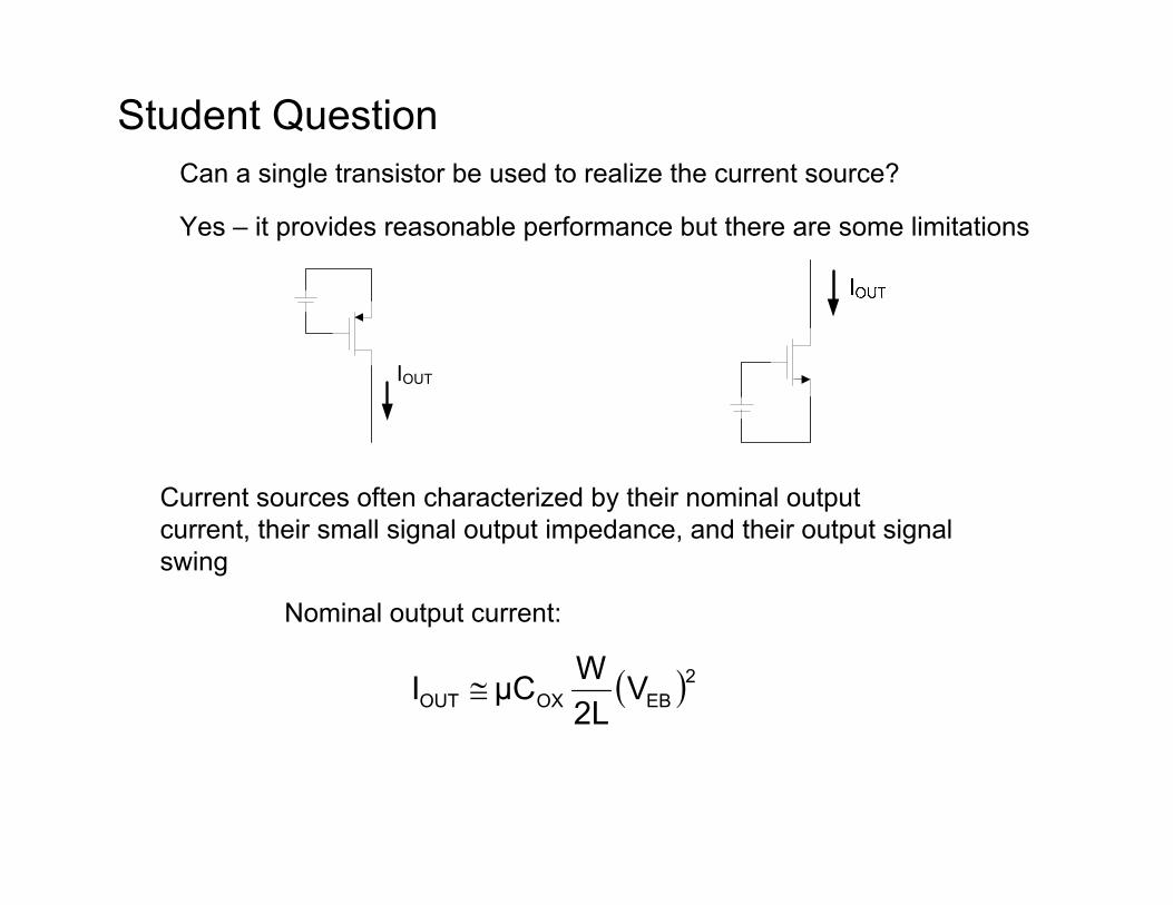
Student Question
IOUT
Can a single transistor be used to realize the current source?
Yes – it provides reasonable performance but there are some limitations
( )2EBOXOUT V2LWµCI ≅
Current sources often characterized by their nominal output current, their small signal output impedance, and their output signal swing
Nominal output current:

Student QuestionCan a single transistor be used to realize the current source?
Output impedance:
i
V
iv
=outR

Student QuestionCan a single transistor be used to realize the current source?
Output signal swing:
To maintain saturation region operation
VDS>VGS-VT
VOUT>VXX-VT
OUT
XX
OUT
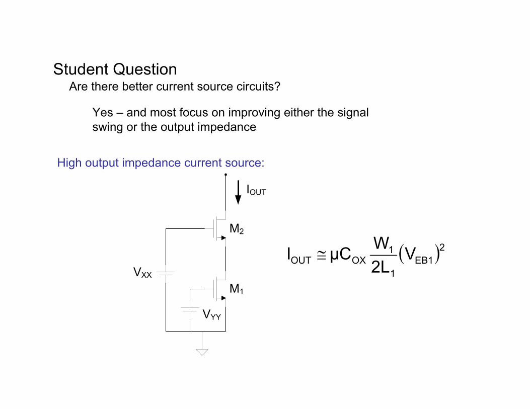
Student Question
1
2
XX
YY
OUT
Are there better current source circuits?
High output impedance current source:
Yes – and most focus on improving either the signal swing or the output impedance
( )2EB11
1OXOUT V
2LWµCI ≅

Student Question
M1
M2
VXX
VYY
IOUT
Are there better current source circuits?
Output Impedance:
i
V
iv
=outR

Student QuestionAre there better current source circuits?
Output Impedance:
iv
=outR
( )( )
⎪⎭
⎪⎬
⎫
−=
+=+
+−=
21
222211
2221
gs
ogsmoo
gsmo
vv
vgvgggv
vggvvi
⎥⎦
⎤⎢⎣
⎡>>⎥
⎦
⎤⎢⎣
⎡≅
+++
==12
2
121
212 11
oo
m
ooo
oomout gg
gggg
gggivR