Embed Size (px)
Citation preview

Air Force Institute of TechnologyAFIT Scholar
Theses and Dissertations Student Graduate Works
3-26-2015
Biaxial Anisotropic Material Development andCharacterization using Rectangular to SquareWaveguideAlexander G. Knisely
Follow this and additional works at: https://scholar.afit.edu/etd
This Thesis is brought to you for free and open access by the Student Graduate Works at AFIT Scholar. It has been accepted for inclusion in Theses andDissertations by an authorized administrator of AFIT Scholar. For more information, please contact [email protected].
Recommended CitationKnisely, Alexander G., "Biaxial Anisotropic Material Development and Characterization using Rectangular to Square Waveguide"(2015). Theses and Dissertations. 40.https://scholar.afit.edu/etd/40
BIAXIAL ANISOTROPICMATERIAL DEVELOPMENT AND
CHARACTERIZATION USINGRECTANGULAR TO SQUARE WAVEGUIDE
THESIS
Alexander G. Knisely
AFIT-ENG-MS-15-M-055
DEPARTMENT OF THE AIR FORCEAIR UNIVERSITY
AIR FORCE INSTITUTE OF TECHNOLOGY
Wright-Patterson Air Force Base, Ohio
DISTRIBUTION STATEMENT AAPPROVED FOR PUBLIC RELEASE; DISTRIBUTION UNLIMITED.

The views expressed in this document are those of the author and do not reflect theofficial policy or position of the United States Air Force, the United States Departmentof Defense or the United States Government. This material is declared a work of theU.S. Government and is not subject to copyright protection in the United States.
AFIT-ENG-MS-15-M-055
BIAXIAL ANISOTROPIC
MATERIAL DEVELOPMENT AND CHARACTERIZATION USING
RECTANGULAR TO SQUARE WAVEGUIDE
THESIS
Presented to the Faculty
Department of Electrical and Computer Engineering
Graduate School of Engineering and Management
Air Force Institute of Technology
Air University
Air Education and Training Command
in Partial Fulfillment of the Requirements for the
Degree of Master of Science in Electrical Engineering
Alexander G. Knisely, B.S.E.E.
March 2015
DISTRIBUTION STATEMENT AAPPROVED FOR PUBLIC RELEASE; DISTRIBUTION UNLIMITED.
AFIT-ENG-MS-15-M-055
BIAXIAL ANISOTROPIC
MATERIAL DEVELOPMENT AND CHARACTERIZATION USING
RECTANGULAR TO SQUARE WAVEGUIDE
THESIS
Alexander G. Knisely, B.S.E.E.
Committee Membership:
Dr. Michael J. HavrillaChair
Dr. Peter J. CollinsMember
Maj Milo W. Hyde, PhDMember
AFIT-ENG-MS-15-M-055
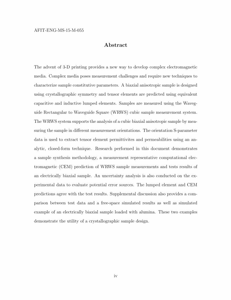
Abstract
The advent of 3-D printing provides a new way to develop complex electromagnetic
media. Complex media poses measurement challenges and require new techniques to
characterize sample constitutive parameters. A biaxial anisotropic sample is designed
using crystallographic symmetry and tensor elements are predicted using equivalent
capacitive and inductive lumped elements. Samples are measured using the Waveg-
uide Rectangular to Waveguide Square (WRWS) cubic sample measurement system.
The WRWS system supports the analysis of a cubic biaxial anisotropic sample by mea-
suring the sample in different measurement orientations. The orientation S-parameter
data is used to extract tensor element permittivites and permeabilities using an an-
alytic, closed-form technique. Research performed in this document demonstrates
a sample synthesis methodology, a measurement representative computational elec-
tromagnetic (CEM) prediction of WRWS sample measurements and tests results of
an electrically biaxial sample. An uncertainty analysis is also conducted on the ex-
perimental data to evaluate potential error sources. The lumped element and CEM
predictions agree with the test results. Supplemental discussion also provides a com-
parison between test data and a free-space simulated results as well as simulated
example of an electrically biaxial sample loaded with alumina. These two examples
demonstrate the utility of a crystallographic sample design.
iv

AFIT-ENG-MS-15-M-055
To my family.
v

Acknowledgements
I would like to thank Dr. Michael J. Havrilla, Dr. Peter J. Collins and Dr. Milo
W. Hyde IV. Each of you provided the physical insight, mathematical rigor and
uniqueness, which I utilized in this work and will continue to practice in my future
endeavors. Also, special thanks to Dr. Jeffery W. Allen for providing test samples,
and Dr. Andrew E. Bogle for providing another perspective.
Alexander G. Knisely
vi

Table of Contents
Page
Abstract . . . . . . . . . . . . . . . . . . . . . . . . . . . . . . . . . . . . . . . . . . . . . . . . . . . . . . . . . . . . . . . iv
Acknowledgements . . . . . . . . . . . . . . . . . . . . . . . . . . . . . . . . . . . . . . . . . . . . . . . . . . . . . . vi
List of Figures . . . . . . . . . . . . . . . . . . . . . . . . . . . . . . . . . . . . . . . . . . . . . . . . . . . . . . . . . . ix
List of Tables . . . . . . . . . . . . . . . . . . . . . . . . . . . . . . . . . . . . . . . . . . . . . . . . . . . . . . . . . . xiii
I. Introduction . . . . . . . . . . . . . . . . . . . . . . . . . . . . . . . . . . . . . . . . . . . . . . . . . . . . . . . . 1
1.1 Problem Statement . . . . . . . . . . . . . . . . . . . . . . . . . . . . . . . . . . . . . . . . . . . . . . 11.2 Scope and Research Goals . . . . . . . . . . . . . . . . . . . . . . . . . . . . . . . . . . . . . . . . 11.3 Limitations and Challenges . . . . . . . . . . . . . . . . . . . . . . . . . . . . . . . . . . . . . . . 31.4 Resource Requirements . . . . . . . . . . . . . . . . . . . . . . . . . . . . . . . . . . . . . . . . . . . 41.5 Thesis Organization . . . . . . . . . . . . . . . . . . . . . . . . . . . . . . . . . . . . . . . . . . . . . 4
II. Background . . . . . . . . . . . . . . . . . . . . . . . . . . . . . . . . . . . . . . . . . . . . . . . . . . . . . . . . 6
2.1 Overview of Material Measurement Techniques . . . . . . . . . . . . . . . . . . . . . . 62.2 Anisotropic Materials . . . . . . . . . . . . . . . . . . . . . . . . . . . . . . . . . . . . . . . . . . . 112.3 Biaxial Anisotropic Material Selection and Research
Usage . . . . . . . . . . . . . . . . . . . . . . . . . . . . . . . . . . . . . . . . . . . . . . . . . . . . . . . . . 122.4 TEM waves at an Oblique Incidence on a Biaxial
Anisotropic Slab . . . . . . . . . . . . . . . . . . . . . . . . . . . . . . . . . . . . . . . . . . . . . . . 13Field Analysis . . . . . . . . . . . . . . . . . . . . . . . . . . . . . . . . . . . . . . . . . . . . . . . . . 14Evaluation of the Parallel Polarization . . . . . . . . . . . . . . . . . . . . . . . . . . . . 20Evaluation of the Perpendicular Polarization . . . . . . . . . . . . . . . . . . . . . . . 23
2.5 Demonstration of Biaxial Anisotropic Slab Performance . . . . . . . . . . . . . 252.6 Summary . . . . . . . . . . . . . . . . . . . . . . . . . . . . . . . . . . . . . . . . . . . . . . . . . . . . . 28
III. Measurement Methodology . . . . . . . . . . . . . . . . . . . . . . . . . . . . . . . . . . . . . . . . . . 29
3.1 Waveguide Rectangular to Waveguide SquareDevelopment . . . . . . . . . . . . . . . . . . . . . . . . . . . . . . . . . . . . . . . . . . . . . . . . . . . 29
3.2 Evaluation of Rectangular Waveguide and WRWS . . . . . . . . . . . . . . . . . . 343.3 Inverse Problem: Biaxial Parameter Extraction . . . . . . . . . . . . . . . . . . . . . 373.4 Summary . . . . . . . . . . . . . . . . . . . . . . . . . . . . . . . . . . . . . . . . . . . . . . . . . . . . . 43
IV. Sample Development . . . . . . . . . . . . . . . . . . . . . . . . . . . . . . . . . . . . . . . . . . . . . . . . 46
4.1 Biaxial Sample Development . . . . . . . . . . . . . . . . . . . . . . . . . . . . . . . . . . . . . 464.2 Lumped Element Prediction of Biaxial Anisotropic
Constitutive Parameters . . . . . . . . . . . . . . . . . . . . . . . . . . . . . . . . . . . . . . . . . 50Sample Analysis Methodology . . . . . . . . . . . . . . . . . . . . . . . . . . . . . . . . . . . . 51
vii
Page
Sample Synthesis Methodology . . . . . . . . . . . . . . . . . . . . . . . . . . . . . . . . . . . 544.3 Computational Electromagnetic Prediction of Biaxial
Anisotropic Constitutive Parameters . . . . . . . . . . . . . . . . . . . . . . . . . . . . . . 56Simulation calibration and sample measurement . . . . . . . . . . . . . . . . . . . . 59TRL Calibration Material Parameter Extraction . . . . . . . . . . . . . . . . . . . . 64
4.4 Summary . . . . . . . . . . . . . . . . . . . . . . . . . . . . . . . . . . . . . . . . . . . . . . . . . . . . . 65
V. Results . . . . . . . . . . . . . . . . . . . . . . . . . . . . . . . . . . . . . . . . . . . . . . . . . . . . . . . . . . . 66
5.1 The WRWS system . . . . . . . . . . . . . . . . . . . . . . . . . . . . . . . . . . . . . . . . . . . . . 665.2 Calibration and Measurement . . . . . . . . . . . . . . . . . . . . . . . . . . . . . . . . . . . . 675.3 CST Model WRWS Model Simulation . . . . . . . . . . . . . . . . . . . . . . . . . . . . . 705.4 Measurement Uncertainty Analysis . . . . . . . . . . . . . . . . . . . . . . . . . . . . . . . 755.5 Observations and Discussion . . . . . . . . . . . . . . . . . . . . . . . . . . . . . . . . . . . . . 825.6 Electrically Biaxial Anisotropic Samples using different
materials . . . . . . . . . . . . . . . . . . . . . . . . . . . . . . . . . . . . . . . . . . . . . . . . . . . . . . 835.7 Summary . . . . . . . . . . . . . . . . . . . . . . . . . . . . . . . . . . . . . . . . . . . . . . . . . . . . . 84
VI. Conclusion . . . . . . . . . . . . . . . . . . . . . . . . . . . . . . . . . . . . . . . . . . . . . . . . . . . . . . . . 85
6.1 Future Work . . . . . . . . . . . . . . . . . . . . . . . . . . . . . . . . . . . . . . . . . . . . . . . . . . . 85Bibliography . . . . . . . . . . . . . . . . . . . . . . . . . . . . . . . . . . . . . . . . . . . . . . . . . . . . . . . . . . . 87
viii

List of Figures
Figure Page
1. Drawing of Waveguide Rectangular to WaveguideSquare (WRWS) System . . . . . . . . . . . . . . . . . . . . . . . . . . . . . . . . . . . . . . . . . . 2
2. Rectangular Waveguide Anisotropic SampleMeasurement . . . . . . . . . . . . . . . . . . . . . . . . . . . . . . . . . . . . . . . . . . . . . . . . . . . . 9
3. Evolution of WRWS system . . . . . . . . . . . . . . . . . . . . . . . . . . . . . . . . . . . . . . 10
4. Demonstrating Collin’s Sample Design is BiaxialAnisotropic . . . . . . . . . . . . . . . . . . . . . . . . . . . . . . . . . . . . . . . . . . . . . . . . . . . . 12
5. 2-D Biaxial Slab problem . . . . . . . . . . . . . . . . . . . . . . . . . . . . . . . . . . . . . . . . 13
6. Left: 3-D MATLABr Plot of Electric Field Responsefrom a Biaxial Anisotropic Slab with constitutivetensors (2.71). Right Top: Transmitted EllipticalPolarization, Right Bottom: Reflected EllipticalPolarization. . . . . . . . . . . . . . . . . . . . . . . . . . . . . . . . . . . . . . . . . . . . . . . . . . . . 26
7. Top: Biaxial Slab with constitutive tensors (2.71) withNormal Incidence Electric Field at Slant polarization.Left: Parallel polarization only, Right Perpendicularpolarization only. . . . . . . . . . . . . . . . . . . . . . . . . . . . . . . . . . . . . . . . . . . . . . . 27
8. TE10 modes propagating in a Rectangular Waveguideand WRWS Transition guide . . . . . . . . . . . . . . . . . . . . . . . . . . . . . . . . . . . . . 34
9. Comparison of Magnitude S-parameter Data:Top-Transmission, Bottom-Reflection . . . . . . . . . . . . . . . . . . . . . . . . . . . . . . 35
10. Comparison of Modes Propagated versus Frequency:Top: Rectangular Waveguide, Bottom: SquareWaveguide . . . . . . . . . . . . . . . . . . . . . . . . . . . . . . . . . . . . . . . . . . . . . . . . . . . . . 36
11. Waveguide arrangement . . . . . . . . . . . . . . . . . . . . . . . . . . . . . . . . . . . . . . . . . 36
12. Sample filled section of waveguide . . . . . . . . . . . . . . . . . . . . . . . . . . . . . . . . . 38
13. Unit Cell Cubic Sample . . . . . . . . . . . . . . . . . . . . . . . . . . . . . . . . . . . . . . . . . 40
14. Closed form measurement with sample resonances at nλ2
. . . . . . . . . . . . . 42
ix
Figure Page
15. Comparison of RWG and WRWS with Free-space filledsample holder: Left: S11, Right: S21 . . . . . . . . . . . . . . . . . . . . . . . . . . . . . . . 43
16. Isotropic UV cured RWG (Top) and WRWS (Bottom)polymer samples and sample holders . . . . . . . . . . . . . . . . . . . . . . . . . . . . . . 44
17. Isotropic UV cured RWG and WRWS polymer samplecomparison . . . . . . . . . . . . . . . . . . . . . . . . . . . . . . . . . . . . . . . . . . . . . . . . . . . . 45
18. Demonstrates Curies Principle and show the symmetrythat exists in each structure. . . . . . . . . . . . . . . . . . . . . . . . . . . . . . . . . . . . . . 47
19. Equivalent Lumped Element Prediction Technique:Left: Permittivity, Right: Permeability . . . . . . . . . . . . . . . . . . . . . . . . . . . . 51
20. Sample and Sample Holder . . . . . . . . . . . . . . . . . . . . . . . . . . . . . . . . . . . . . . . 55
21. CST models of Rectangular Waveguide and WRWSsystem (Left), Teflon Samples installed (Right) . . . . . . . . . . . . . . . . . . . . . 57
22. CST WRWS Teflon Sample De-embedded . . . . . . . . . . . . . . . . . . . . . . . . . . 58
23. Graphical Depiction of TRL calibration . . . . . . . . . . . . . . . . . . . . . . . . . . . . 60
24. Sample Holder with dimensions . . . . . . . . . . . . . . . . . . . . . . . . . . . . . . . . . . . 63
25. Rectangular Waveguide Teflon Sample TRL CalibratedSolution . . . . . . . . . . . . . . . . . . . . . . . . . . . . . . . . . . . . . . . . . . . . . . . . . . . . . . . 64
26. WRWS setup and view of square aperture . . . . . . . . . . . . . . . . . . . . . . . . . 66
27. WRWS Cubic Sample Holder and Line Standard . . . . . . . . . . . . . . . . . . . . 67
28. WRWS showing waveguide transition on either side ofthe sample holder, line standard is placed left of sampleholder . . . . . . . . . . . . . . . . . . . . . . . . . . . . . . . . . . . . . . . . . . . . . . . . . . . . . . . . . 68
29. Measurement Setup with Test port cables and NetworkAnalyzer . . . . . . . . . . . . . . . . . . . . . . . . . . . . . . . . . . . . . . . . . . . . . . . . . . . . . . 69
30. Sample installed in Sample Holder Orientation 1 (Left),Partially installed in Orientation 2 (Right) . . . . . . . . . . . . . . . . . . . . . . . . . 70
31. CST Model of WRWS with a green cube denotingsample region . . . . . . . . . . . . . . . . . . . . . . . . . . . . . . . . . . . . . . . . . . . . . . . . . . 71
x
Figure Page
32. CST WRWS Model in mesh view . . . . . . . . . . . . . . . . . . . . . . . . . . . . . . . . . 72
33. Measured Permittivity from Electrically BiaxialAnisotropic Cube with Air Occlusions arranged in a 9by 6 array . . . . . . . . . . . . . . . . . . . . . . . . . . . . . . . . . . . . . . . . . . . . . . . . . . . . . 74
34. CST Simulated Permittivity from Electrically BiaxialAnisotropic Cube with Air Occlusions arranged in a 9by 6 array . . . . . . . . . . . . . . . . . . . . . . . . . . . . . . . . . . . . . . . . . . . . . . . . . . . . . 74
35. Monte Carlo Uncertainty Analysis Flow Chart: Goldindicates random test variables, Green- Test DataInputs, Orange- Outputs, Blue- Code. Bi-directionalarrows associated with the calibration code indicate aspecific uncertainty is obtained given a particulartransmission or reflection coefficient. . . . . . . . . . . . . . . . . . . . . . . . . . . . . . . 75
36. VNA Uncertainty vs Reflection (Top) and Transmission(Bottom) generated for the Agilent Technologiesr
E8362B VNA from the Keysight Technologiesr VNAuncertainty calculator. . . . . . . . . . . . . . . . . . . . . . . . . . . . . . . . . . . . . . . . . . . 76
37. Cubic sample (blue) with colored gaps regions. Thecolored regions show how gaps are accounted in theMonte Carlo Simulation . . . . . . . . . . . . . . . . . . . . . . . . . . . . . . . . . . . . . . . . . 77
38. Error Bars Generated from 1000 trial Monte Carlo onExperimental Data, Odd orientations (Top), Evenorientations (Bottom) . . . . . . . . . . . . . . . . . . . . . . . . . . . . . . . . . . . . . . . . . . . 79
39. Comparison of Simulation Data with ExperimentalUncertainty Data Odd orientations (Top), Evenorientations (Bottom) . . . . . . . . . . . . . . . . . . . . . . . . . . . . . . . . . . . . . . . . . . . 80
40. Comparison of Vertical arrangement Lumped ElementData and Simulation Data with ExperimentalUncertainty Data Odd orientations (Top), Evenorientations (Bottom) . . . . . . . . . . . . . . . . . . . . . . . . . . . . . . . . . . . . . . . . . . . 81
41. Overlay of sample measurement orientations with TE10
mode profile showing potential non-uniforminterrogation of sample . . . . . . . . . . . . . . . . . . . . . . . . . . . . . . . . . . . . . . . . . . 82
42. TEM Free Space CST Measure of an infinite array ofcubes arranged in a slab . . . . . . . . . . . . . . . . . . . . . . . . . . . . . . . . . . . . . . . . . 83
xi

Figure Page
43. Plane Wave Excitation Model on an infinite array ofcubes . . . . . . . . . . . . . . . . . . . . . . . . . . . . . . . . . . . . . . . . . . . . . . . . . . . . . . . . . 84
44. Electrically Biaxial Alumina Inclusion Loaded Samplesimulated in CST Microwave Studio . . . . . . . . . . . . . . . . . . . . . . . . . . . . . . 84
xii

List of Tables
Table Page
1. Vertical Lumped Element Prediction . . . . . . . . . . . . . . . . . . . . . . . . . . . . . . 56
2. Horizontal Lumped Element Prediction . . . . . . . . . . . . . . . . . . . . . . . . . . . . 56
3. CST Simulation Performance Figures . . . . . . . . . . . . . . . . . . . . . . . . . . . . . 73
xiii
BIAXIAL ANISOTROPIC
MATERIAL DEVELOPMENT AND CHARACTERIZATION USING
RECTANGULAR TO SQUARE WAVEGUIDE
I. Introduction
1.1 Problem Statement
Advances in 3 dimensional (3-D) printing offer a new and unique microwave mate-
rial development capability. Sub-wavelength features can be easily printed and imple-
mented into microwave system designs. These sub-wavelength features can support
a wide variety of material performance characteristics. New electromagnetic mate-
rial performance characteristics pose challenges, such as: how to correctly measure
a material and how to design a material with specific performance characteristics?
The complexity of these challenges vary in difficulty depending on the measurement
technique used and the material’s constitutive parameters.
1.2 Scope and Research Goals
Electromagnetic materials can include characteristics ranging in Linearity, Ho-
mogeneity, Isotropy and Reciprocity. Evaluating materials based on isotropy versus
measurement complexity, isotropic materials are the simplest to evaluate followed by
bi-isotropic, anisotropic and bi-anisotropic. Each category requires additional unique
measurements to successfully evaluate the constitutive material parameters. Unique
measurement information come from measurement system degrees of freedom includ-
ing: evaluating the sample in different orientations, or interrogating the sample with
1
different field polarizations.
A new waveguide material measurement system is developed in this research ef-
fort to evaluate a single sample about different orientations. The waveguide method
is selected because a Thru-Reflect-Line (TRL) calibration can be utilized and mea-
surements can be made at the fundamental TE10 mode, which supports closed form
solutions to obtain material permittivity and permeability constitutive parameters.
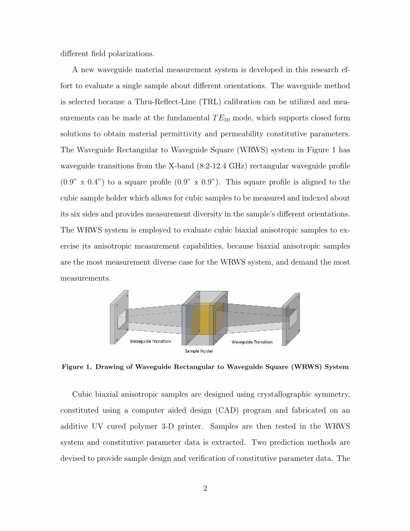
The Waveguide Rectangular to Waveguide Square (WRWS) system in Figure 1 has
waveguide transitions from the X-band (8.2-12.4 GHz) rectangular waveguide profile
(0.9” x 0.4”) to a square profile (0.9” x 0.9”). This square profile is aligned to the
cubic sample holder which allows for cubic samples to be measured and indexed about
its six sides and provides measurement diversity in the sample’s different orientations.
The WRWS system is employed to evaluate cubic biaxial anisotropic samples to ex-
ercise its anisotropic measurement capabilities, because biaxial anisotropic samples
are the most measurement diverse case for the WRWS system, and demand the most
measurements.
Figure 1. Drawing of Waveguide Rectangular to Waveguide Square (WRWS) System
Cubic biaxial anisotropic samples are designed using crystallographic symmetry,
constituted using a computer aided design (CAD) program and fabricated on an
additive UV cured polymer 3-D printer. Samples are then tested in the WRWS
system and constitutive parameter data is extracted. Two prediction methods are
devised to provide sample design and verification of constitutive parameter data. The
2
first method is a capacitive and inductive lumped element equivalent circuit design
model, and the second method is a computation electromagnetic (CEM) solver model
developed in CST Microwave Studior .
The goal of this research is to demonstrate the WRWS system as a closed form
method for measuring engineered biaxial anisotropic materials and demonstrate a
crystallographic design methodology. Success is measured by comparing the experi-
mentally extracted constitutive parameter data against the two prediction methods.
Additionally, a TRL calibration technique is used to accommodate systematic er-
rors and an uncertainty analysis is conducted to evaluate the effects of random error
sources in the WRWS system.
1.3 Limitations and Challenges
Biaxial anisotropic measurement and material design are the focus of this research
because it constrains measurement diversity in evaluating a sample about different
orientations. Biaxial anisotropic materials consist of materials which have permittiv-
ity↔ε and permeability
↔µ represented by
↔ε =
εxx 0 0
0 εyy 0
0 0 εzz
,↔µ =
µxx 0 0
0 µyy 0
0 0 µzz
. (1.1)
which posses tensor elements that are orthogonal and unique about the sample’s x,
y and z axes (assuming alignment along the optic axis).
The challenges in biaxial anisotropic research are in devising an accurate material
characterization method and designing a material which exhibits biaxial anisotropic
performance. Because the WRWS system accommodates a 0.9” edge length cubic
sample, the sample is electrically thick at X-band which poses λ2
resonance issues.
3

These resonances occur at frequencies in which the S11 measurement approaches
zero, resulting in singularities in the closed form solutions for permittivity and per-
meability. A methodology for avoiding the resonance issue is to implement a root
search method and assume particular permittivity or permeability values. Knowing
a sample’s relative permeability, and guessing a relative permittivity allows for a root
search to be performed on the S21 data and yields resonance free permittivity results.
The same root search process can be performed obtaining a sample’s permeability, if
the permittivity is known and a guess is made on a samples permeability. The root
search process avoids using both sets of S-parameter data and yields valid resonance
free results. Because dielectric materials are readily available and easier to manipulate
than magnetic samples, electrically biaxial anisotropic samples having permeability
µ0 are only considered in this research. Other material designs are discussed in the
future work section.
1.4 Resource Requirements
The Air Force Institute of Technology (AFIT) material measurements laboratory
possesses Vector Network Analyzers, microwave measurement support tooling, the
WRWS measurement system, and CST Microwave Studior licenses to support the
CEM analysis. Additionally, AFIT partnership with Air Force Research Laboratory
(AFRL), Sensors Directorate, Electromagnetics Research Branch has yielded the abil-
ity to fabricate material samples using their ultraviolet (UV) cured ink-jet type 3-D
polymer printer.
1.5 Thesis Organization
This document describes the research and development of the WRWS anisotropic
material measurement capability and an electrically biaxial anisotropic material.
4
Chapter 2 provides background information on waveguide material measurement ca-
pabilities and shows how the evolution and performance trade-offs in waveguide ma-
terial measurement techniques lead to the WRWS design. A theoretical model of a
biaxial anisotropic slab is developed to demonstrate the unique performance charac-
teristics of a biaxial anisotropic material and discuss how the material is evaluated in
the WRWS system. Chapter 3 provides an analysis of a rectangular waveguide filled
with biaxial anisotropic material. A closed-form Nicolson-Ross-Wier type formula-
tion is also derived for the WRWS system. A comparison between the rectangular
waveguide profile, and the square sample holder profile is also performed to demon-
strate the operational modes, and to show the appropriate measurement frequencies.
Chapter 4 addresses a crystallographic sample design, fabrication, constitutive param-
eter prediction techniques and the implementation of a TRL calibration. Chapter 5
demonstrates the experimental measurement capabilities, evaluating the sources of
measurement errors in an uncertainty analysis and compares the measured data to
the predicted data. Chapter 6 provides a conclusion, remarks and suggestions for
future work.
5
II. Background
Research into waveguide material measurement theory and anisotropic sample
design is conducted to understand the historical progression of anisotropic mate-
rial measurement and development research. Waveguide material measurement tech-
niques, crystallographic sample design and electromagnetic material development are
studied and the gained knowledge is applied toward the development of the WRWS
anisotropic measurement capability and biaxial anisotropic sample characterization.
Additionally, a 2 dimensional (2-D) free-space analysis of an infinite biaxial slab is
performed to understand the transmitted and reflected field effects from a slab of
biaxial anisotropic material. The results of the 2-D analysis demonstrate potential
applications for a biaxial anisotropic material and show how the constitutive param-
eters are extracted in particular measurement scenarios.
2.1 Overview of Material Measurement Techniques
Waveguide material measurement techniques became prevalent with the works of
Nicolson, Ross and Weir, (NRW)[1],[2]. Their research demonstrate a fundamental
approach to material characterization. Material characterization requires that a for-
ward problem be developed, which describes the fields, boundary conditions and the
media regions involved in the measurement system. This forward problem yields con-
straint equations, and identifies how the measurable quantities, namely, Transmission
(T ) and Reflection (Γ) coefficients, are related to permittivity and permeability. The
reflection and transmission coefficients are measured directly as S-parameters using
a Vector Network Analyzer, where T is equivalent to S21 and Γ is S11. The forward
6
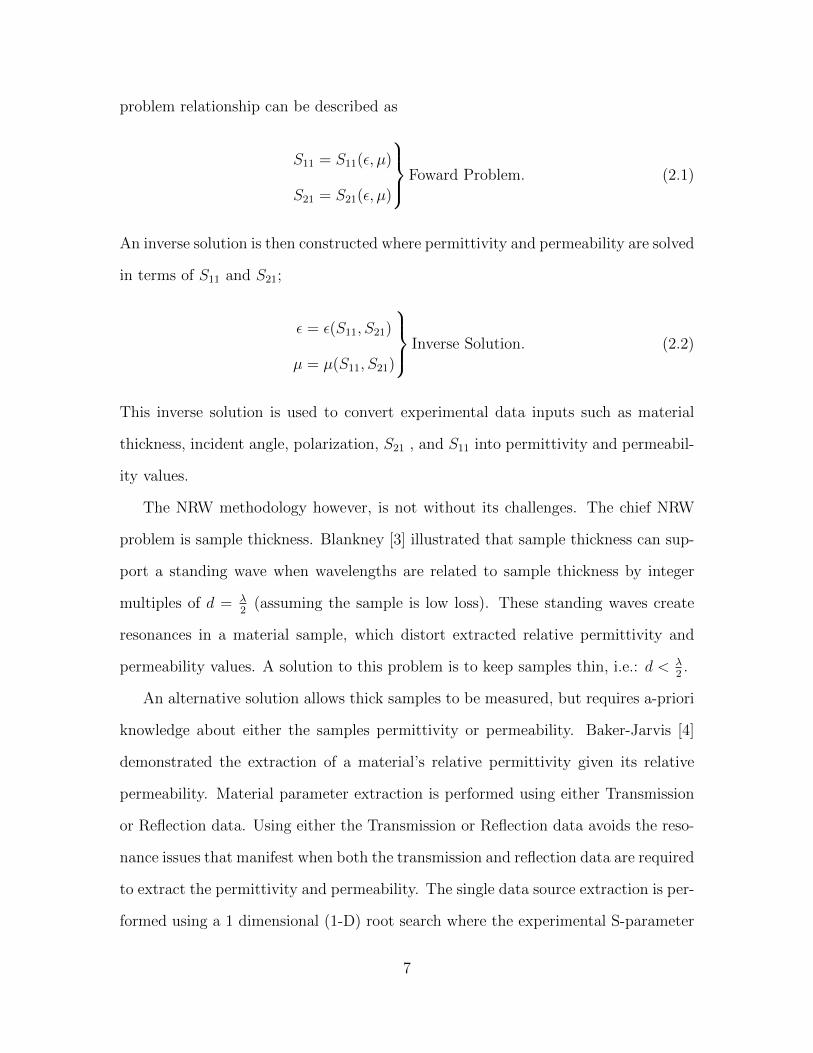
problem relationship can be described as
S11 = S11(ε, µ)
S21 = S21(ε, µ)
Foward Problem. (2.1)
An inverse solution is then constructed where permittivity and permeability are solved
in terms of S11 and S21;
ε = ε(S11, S21)
µ = µ(S11, S21)
Inverse Solution. (2.2)
This inverse solution is used to convert experimental data inputs such as material
thickness, incident angle, polarization, S21 , and S11 into permittivity and permeabil-
ity values.
The NRW methodology however, is not without its challenges. The chief NRW
problem is sample thickness. Blankney [3] illustrated that sample thickness can sup-
port a standing wave when wavelengths are related to sample thickness by integer
multiples of d = λ2
(assuming the sample is low loss). These standing waves create
resonances in a material sample, which distort extracted relative permittivity and
permeability values. A solution to this problem is to keep samples thin, i.e.: d < λ2.
An alternative solution allows thick samples to be measured, but requires a-priori
knowledge about either the samples permittivity or permeability. Baker-Jarvis [4]
demonstrated the extraction of a material’s relative permittivity given its relative
permeability. Material parameter extraction is performed using either Transmission
or Reflection data. Using either the Transmission or Reflection data avoids the reso-
nance issues that manifest when both the transmission and reflection data are required
to extract the permittivity and permeability. The single data source extraction is per-
formed using a 1 dimensional (1-D) root search where the experimental S-parameter
7

value is compared to a theoretical S-parameter value based on an initial guess of the
permittivity. Subsequent iterations are made based on the difference in the experi-
mental and theoretical S-parameters values, until a permittivity accuracy threshold
is achieved.
All of the aforementioned work focused on solving measurement problems in
isotropic materials. The construct of a Forward Problem development and Inverse
Solution extraction can be applied to any material characterization problem, as long
as the measurement technique and type of Material Under Test (MUT) is accurately
posed. The forward problem complexity increases as the type of MUT changes from
isotropic through bi-anisotropic. As a result, the number of unique measurements
needed to solve the inverse solution also increases. Various measurement techniques
are limited by the number of unique measurements that can be performed on a given
sample by a given field applicator. Using traditional rectangular waveguide ma-
terial measurement techniques and the appropriate mathematical material parame-
ter extraction development, poses challenges in anisotropic material characterization,
namely multiple samples are required to provide enough measurement information
as seen in Figure 2. Each sample needs to be a different measurement orientation of
the parent material, so that it properly fits into the rectangular waveguide. A prob-
lem with multiple samples is that it induces measurement error, because each sample
is subject to its own independent error sources. Having multiple samples makes it
difficult to conclusively say that the results of three independent samples are truly
representative of the parent anisotropic material.
Uslenghi [5] demonstrated a potential waveguide measurement capability using
TE10 and TE20 modes for measuring biaxial anisotropic materials. The measurement
procedure suggests using multiple sample orientations to provide sufficient measure-
ment diversity to obtain all of the constitutive tensor elements. However, because of
8
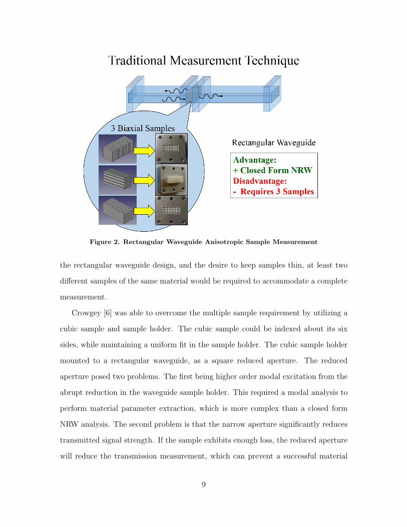
Figure 2. Rectangular Waveguide Anisotropic Sample Measurement
the rectangular waveguide design, and the desire to keep samples thin, at least two
different samples of the same material would be required to accommodate a complete
measurement.
Crowgey [6] was able to overcome the multiple sample requirement by utilizing a
cubic sample and sample holder. The cubic sample could be indexed about its six
sides, while maintaining a uniform fit in the sample holder. The cubic sample holder
mounted to a rectangular waveguide, as a square reduced aperture. The reduced
aperture posed two problems. The first being higher order modal excitation from the
abrupt reduction in the waveguide sample holder. This required a modal analysis to
perform material parameter extraction, which is more complex than a closed form
NRW analysis. The second problem is that the narrow aperture significantly reduces
transmitted signal strength. If the sample exhibits enough loss, the reduced aperture
will reduce the transmission measurement, which can prevent a successful material
9
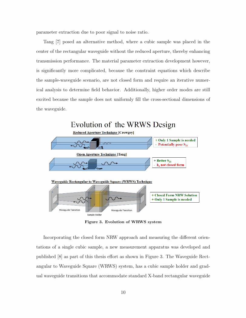
parameter extraction due to poor signal to noise ratio.
Tang [7] posed an alternative method, where a cubic sample was placed in the
center of the rectangular waveguide without the reduced aperture, thereby enhancing
transmission performance. The material parameter extraction development however,
is significantly more complicated, because the constraint equations which describe
the sample-waveguide scenario, are not closed form and require an iterative numer-
ical analysis to determine field behavior. Additionally, higher order modes are still
excited because the sample does not uniformly fill the cross-sectional dimensions of
the waveguide.
Figure 3. Evolution of WRWS system
Incorporating the closed form NRW approach and measuring the different orien-
tations of a single cubic sample, a new measurement apparatus was developed and
published [8] as part of this thesis effort as shown in Figure 3. The Waveguide Rect-
angular to Waveguide Square (WRWS) system, has a cubic sample holder and grad-
ual waveguide transitions that accommodate standard X-band rectangular waveguide
10

and the cubic sample holder. These gradual transitions ensure that only the funda-
mental TE10 mode is excited and supports closed form, analytic solutions for biaxial
anisotropic material parameter extraction. The WRWS system is addressed in the re-
maining chapters and utilized for making biaxial anisotropic material measurements.
2.2 Anisotropic Materials
Early developments in engineered microwave anisotropic materials are discussed
in Collin’s work [9]. Collin provides several theoretical developments that are used
in anisotropic material design. He posed that isotropic materials of different per-
mittivities and permeabilities could be used in combinations to synthesize different
anisotropic effects. A requirement was also identified, which says that the mate-
rial arrangements must be electrically small with respect to the intended operat-
ing frequency. Specifically, inclusions or the combination of two materials need to
be “less than about 310λ” [9] to adhere to macroscopic electromagnetics. Collin
also demonstrates two geometries which produce anisotropic behavior: A Uniaxial
Anisotropic material made by alternating slabs of two different materials; and a Bi-
axial Anisotropic material made by periodic, uniformly spaced three dimensional
rectangular inclusions inside a host material. This three dimensional rectangular
structure serves as the initial basis for the biaxial material design evaluated in the
WRWS system.
More recently, research by Dmitriev [10] provides guidance on anisotropic material
design by crystallographic symmetry, as opposed to an iterative, trial and error design
methodology. Dmitriev shows that arrangements of different electric and magnetic ge-
ometries with specific symmetries can be used to design different kinds of anisotropy.
Dmitriev utilizes Curie’s and Neumann’s Principles to mathematically predict ma-
terial tensor structure. Crystallographic sample design as shown in Figure 4 is a
11
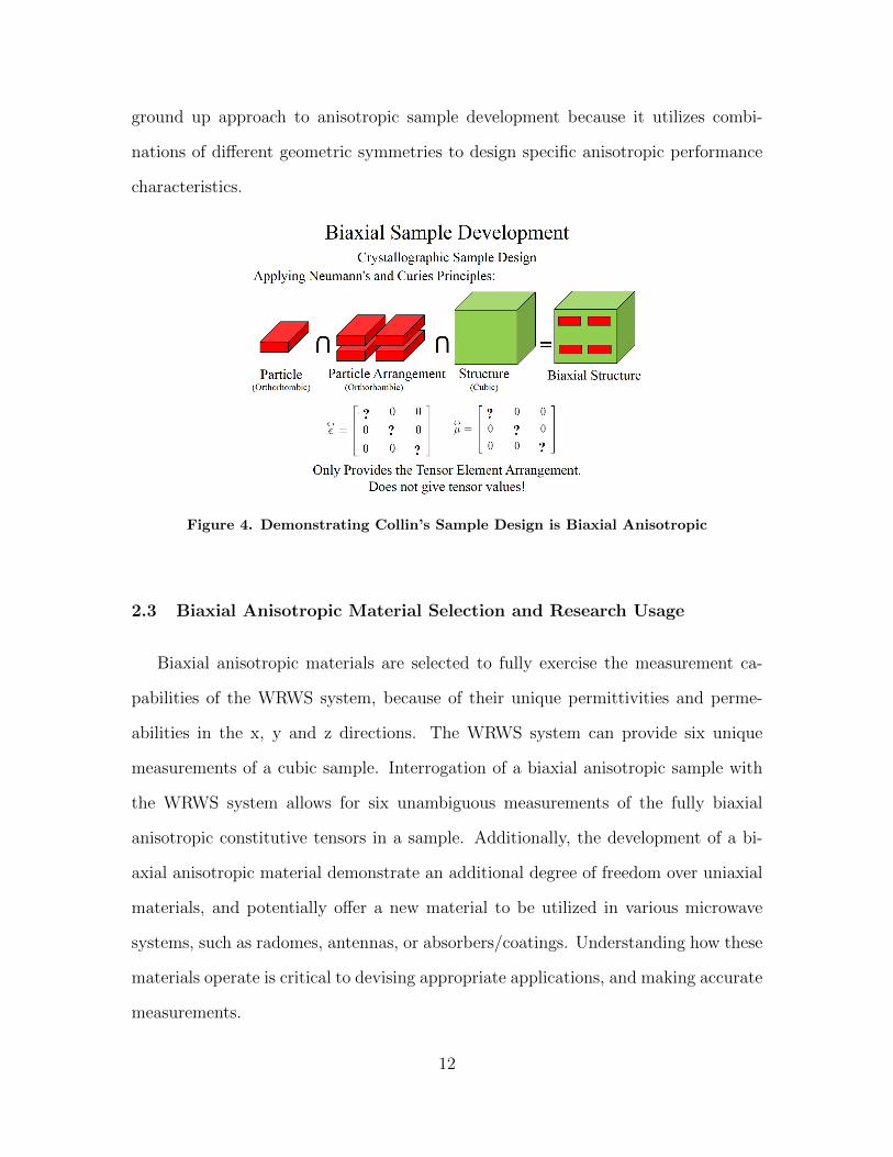
ground up approach to anisotropic sample development because it utilizes combi-
nations of different geometric symmetries to design specific anisotropic performance
characteristics.
Figure 4. Demonstrating Collin’s Sample Design is Biaxial Anisotropic
2.3 Biaxial Anisotropic Material Selection and Research Usage
Biaxial anisotropic materials are selected to fully exercise the measurement ca-
pabilities of the WRWS system, because of their unique permittivities and perme-
abilities in the x, y and z directions. The WRWS system can provide six unique
measurements of a cubic sample. Interrogation of a biaxial anisotropic sample with
the WRWS system allows for six unambiguous measurements of the fully biaxial
anisotropic constitutive tensors in a sample. Additionally, the development of a bi-
axial anisotropic material demonstrate an additional degree of freedom over uniaxial
materials, and potentially offer a new material to be utilized in various microwave
systems, such as radomes, antennas, or absorbers/coatings. Understanding how these
materials operate is critical to devising appropriate applications, and making accurate
measurements.
12
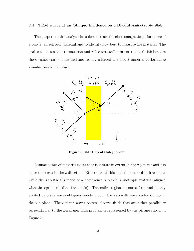
2.4 TEM waves at an Oblique Incidence on a Biaxial Anisotropic Slab
The purpose of this analysis is to demonstrate the electromagnetic performance of
a biaxial anisotropic material and to identify how best to measure the material. The
goal is to obtain the transmission and reflection coefficients of a biaxial slab because
these values can be measured and readily adapted to support material performance
visualization simulations.
Figure 5. 2-D Biaxial Slab problem
Assume a slab of material exists that is infinite in extent in the x-y plane and has
finite thickness in the z direction. Either side of this slab is immersed in free-space,
while the slab itself is made of a homogeneous biaxial anisotropic material aligned
with the optic axis (i.e. the z-axis). The entire region is source free, and is only
excited by plane waves obliquely incident upon the slab with wave vector ~k lying in
the x-z plane. These plane waves possess electric fields that are either parallel or
perpendicular to the x-z plane. This problem is represented by the picture shown in
Figure 5.
13
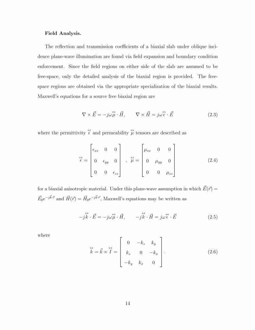
Field Analysis.
The reflection and transmission coefficients of a biaxial slab under oblique inci-
dence plane-wave illumination are found via field expansion and boundary condition
enforcement. Since the field regions on either side of the slab are assumed to be
free-space, only the detailed analysis of the biaxial region is provided. The free-
space regions are obtained via the appropriate specialization of the biaxial results.
Maxwell’s equations for a source free biaxial region are
∇× ~E = −jω↔µ · ~H, ∇× ~H = jω↔ε · ~E (2.3)
where the permittivity↔ε and permeability
↔µ tensors are described as
↔ε =
εxx 0 0
0 εyy 0
0 0 εzz
,↔µ =
µxx 0 0
0 µyy 0
0 0 µzz
(2.4)
for a biaxial anisotropic material. Under this plane-wave assumption in which ~E(~r) =
~E0e−j~k·~r and ~H(~r) = ~H0e
−j~k·~r, Maxwell’s equations may be written as
−j↔k · ~E = −jω↔µ · ~H, −j
↔k · ~H = jω
↔ε · ~E (2.5)
where
↔k = ~k ×
↔I =
0 −kz ky
kz 0 −kx
−ky kx 0
. (2.6)
14

Solving for ~H in Faraday’s Law of (2.5) leads to
~H =1
ω
↔µ−1·↔k · ~E (2.7)
and subsequent insertion into Ampere’s Law yields the wave equation
[−↔µ ·↔k · ↔µ
−1·↔k − ω2↔µ · ↔ε ] · ~E = 0 (2.8)
or↔W · ~E = 0 since e−j
~k·~r 6= 0. Equation (2.8) is an algebraic matrix equation for wave
number kz and has a non-trivial solution only if the determinate of↔W equals zero.
The roots of the characteristic polynomial (i.e. the roots of det↔W = 0) represents the
allowed eigen values (i.e. propagation constants kz). Insertion of these eigen values
into (2.8) lead to the corresponding eigen vectors (i.e. the electric field structure).
Simple matrix operations show that↔W takes on the form
↔W =
kz
2 µxµy− εx µxw2 0 −kx kz µx
µy
0 kx2 µyµz− εy µy w2 + kz
2 µyµx
0
−kx kz µzµy
0 kx2 µzµy− εz µz w2
. (2.9)
Taking the determinate of↔W , and setting it equal to zero leads to the following
allowed eigen values
kz = ±√ω2εxµy − εx
εzk2x
kz = ±√ω2εyµx − µx
µzk2x
. (2.10)
These four solutions for kz give physical insight into how the fields propagate in
biaxial anisotropic media. The solutions ±k‖z = ±√ω2εxµy − εx
εzk2x represent the
forward and reverse propagating waves that are in a parallel polarization state, while
±k⊥z = ±√ω2εyµx − µx
µzk2x represent forward and reverse propagating waves in the
15
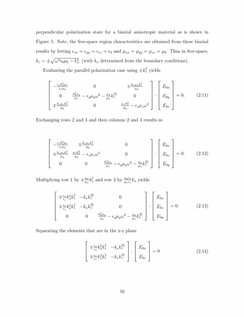
perpendicular polarization state for a biaxial anisotropic material as is shown in
Figure 5. Note, the free-space region characteristics are obtained from these biaxial
results by letting εxx = εyy = εzz = ε0 and µxx = µyy = µzz = µ0. Thus in free-space,
kz = ±√ω2ε0µ0 − k2
x, (with kx determined from the boundary conditions).
Evaluating the parallel polarization case using ±k‖z yields
− εxk2xµx
εzµy0 ∓kxµxk
‖z
µy
0 k2xµyµz− εyµyω2 − µy
µxk
2‖z 0
∓kxµzk‖z
µy0 µzk2x
µy− εzµzω2
·E0x
E0y
E0z
= 0. (2.11)
Exchanging rows 2 and 3 and then columns 2 and 3 results in
− εxk2xµx
εzµy∓kxµxk
‖z
µy0
∓kxµzk‖z
µy
µzk2xµy− εzµzω2 0
0 0 k2xµyµz− εyµyω2 − µy
µxk
2‖z
·E0x
E0z
E0y
= 0. (2.12)
Multiplying row 1 by ±µyµxk‖z and row 2 by µyεx
µxεzkx yields
∓ εxεzk2xk‖z −kxk2‖
z 0
∓ εxεzk2xk‖z −kxk2‖
z 0
0 0 k2xµyµz− εyµyω2 − µy
µxk
2‖z
·E0x
E0z
E0y
= 0. (2.13)
Separating the elements that are in the x-z plane
∓ εxεzk2xk‖z −kxk2‖
z
∓ εxεzk2xk‖z −kxk2‖
z
· E0x
E0z
= 0 (2.14)
16
and the part that is in the y direction
[k2xµyµz− εyµyω2 − µy
µxk2‖z
]·[E0y
]= 0, (2.15)
indicates that the parallel polarization only supports parallel polarization fields, be-
cause E0z = ∓ εxkx
εzk‖z
E0x and E0y = 0. Ey must equal zero because the eigen vector
equaling zero yields a trivial solution. Therefore the fields supported in the par-
allel polarization are ~E = (x ∓ z εxkxεzk
‖z
)E0xe−jkxx∓jk‖zz. Evaluating the perpendicular
polarization case using ±k⊥z yields
k2⊥z µxµy− εx µxw2 0 ∓kx k⊥z µx
µy
0 0 0
∓kx k⊥z µzµy
0 kx2 µzµy− εz µz w2
·E0x
E0y
E0z
= 0. (2.16)
Exchanging rows 2 and 3 and then columns 2 and 3 yields
k2⊥z µxµy− εx µxw2 ∓kx k⊥z µx
µy0
∓kx k⊥z µzµy
kx2 µzµy− εz µz w2 0
0 0 0
·E0x
E0z
E0y
= 0. (2.17)
Multiplying row 1 by ±µyµxk⊥z and row 2 by µy
µzkx yields
∓µxµzk2xk⊥z −kxk2⊥
z 0
±k2xk⊥z −k3
x + kxεzµyω2 0
0 0 0
·E0x
E0z
E0y
= 0. (2.18)
17
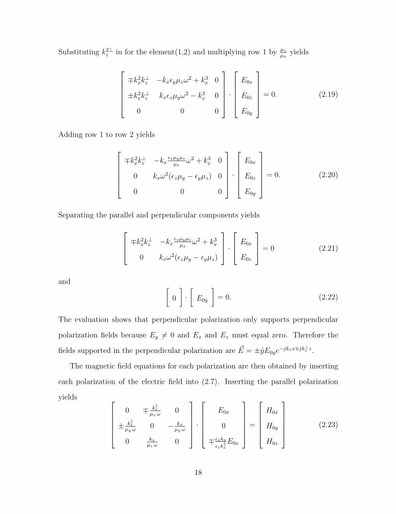
Substituting k2⊥z in for the element(1,2) and multiplying row 1 by µz
µxyields
∓k2
xk⊥z −kxεyµzω2 + k3
x 0
±k2xk⊥z kxεzµyω
2 − k3x 0
0 0 0
·E0x
E0z
E0y
= 0. (2.19)
Adding row 1 to row 2 yields
∓k2
xk⊥z −kx εxµyµzµx
ω2 + k3x 0
0 kxω2(εzµy − εyµz) 0
0 0 0
·E0x
E0z
E0y
= 0. (2.20)
Separating the parallel and perpendicular components yields
∓k2xk⊥z −kx εxµyµzµx
ω2 + k3x
0 kxω2(εzµy − εyµz)
· E0x
E0z
= 0 (2.21)
and [0
]·[E0y
]= 0. (2.22)
The evaluation shows that perpendicular polarization only supports perpendicular
polarization fields because Ey 6= 0 and Ex and Ez must equal zero. Therefore the
fields supported in the perpendicular polarization are ~E = ±yE0ye−jkxx∓jk⊥z z.
The magnetic field equations for each polarization are then obtained by inserting
each polarization of the electric field into (2.7). Inserting the parallel polarization
yields 0 ∓ k
‖z
µx ω0
± k‖z
µy ω0 − kx
µy ω
0 kxµz ω
0
·
E0x
0
∓ εxkx
εzk‖z
E0x
=
H0x
H0y
H0z
(2.23)
18

which results in a y directed magnetic field,
~H = y
(± k
‖z
µy ω± kxµy ω
εxkx
εzk‖z
)E0xe
−jkxx∓jk‖zz (2.24)
and simplifies to
~H = ±y(ωεy
k‖z
)E0xe
−jkxx∓jk‖zz. (2.25)
The wave impedance is defined as the ratio of the tangential electric field over the
tangential magnetic field for a single traveling wave, which yields η‖2 = k
‖z
ωεy. Inserting
the perpendicular polarization yields
0 ∓ k⊥z
µx ω0
± k⊥zµy ω
0 − kxµy ω
0 kxµz ω
0
·
0
±E0y
0
=
H0x
H0y
H0z
(2.26)
which results in a x and z directed magnetic field,
~H =
(∓ k⊥zµx ω
x+kxµz ω
z
)E0ye
−jkxx∓jk⊥z z (2.27)
and simplifies to
~H = ∓ k⊥zµx ω
(x∓ µx
µz
kxk⊥zz
)E0ye
−jkxx∓jk⊥z z. (2.28)
The wave impedance for the perpendicular case is η⊥2 = ωµxk⊥z
. Having the fields,
impedances and propagation constants for each polarization provides the required in-
formation to enforce boundary conditions and solve for the transmission and reflection
coefficients.
Mathematically describing the incident, transmitted and reflected waves featured
by the scenario in Figure 5 yields the follow equations for both the parallel and
perpendicular polarizations. Each polarization is separated and evaluated as its own
19
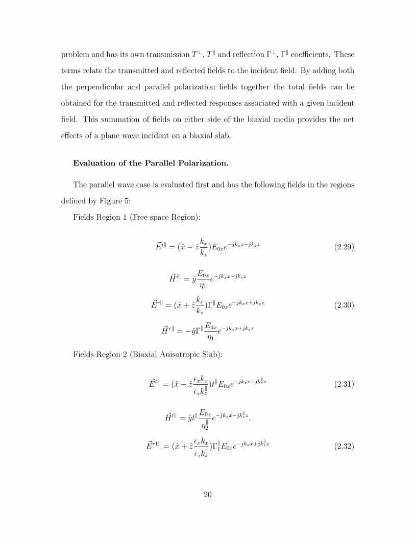
problem and has its own transmission T⊥, T ‖ and reflection Γ⊥, Γ‖ coefficients. These
terms relate the transmitted and reflected fields to the incident field. By adding both
the perpendicular and parallel polarization fields together the total fields can be
obtained for the transmitted and reflected responses associated with a given incident
field. This summation of fields on either side of the biaxial media provides the net
effects of a plane wave incident on a biaxial slab.
Evaluation of the Parallel Polarization.
The parallel wave case is evaluated first and has the following fields in the regions
defined by Figure 5:
Fields Region 1 (Free-space Region):
~Ei‖ = (x− z kxkz
)E0xe−jkxx−jkzz (2.29)
~H i‖ = yE0x
η1
e−jkxx−jkzz
~Er‖ = (x+ zkxkz
)Γ‖E0xe−jkxx+jkzz (2.30)
~Hr‖ = −yΓ‖E0x
η1
e−jkxx+jkzz
Fields Region 2 (Biaxial Anisotropic Slab):
~Et‖ = (x− z εxkxεzk‖z
)t‖E0xe−jkxx−jk‖zz (2.31)
~H t‖ = yt‖E0x
η‖2
e−jkxx−jk‖zz.
~Er1‖ = (x+ zεxkx
εzk‖z
)Γ‖1E0xe
−jkxx+jk‖zz (2.32)
20

~Hr1‖ = −yΓ‖1
E0x
η‖2
e−jkxx+jk‖zz.
Fields Region 3 (Free-space Region):
~ET‖ = (x− z kxkz
)T ‖E0xe−jkxx−jkz(z−d) (2.33)
~HT‖ = yT ‖E0x
η1
e−jkxx−jkz(z−d)
Enforcing the continuity of tangential ~E and ~H at each of the region interfaces
requires that kx = k0 sin θi be equivalent on either side of the interface by Snell’s Law.
Interface 1 (z=0):
1 + Γ‖ = t‖ + Γ‖1 (2.34)
1
η1
(1− Γ‖) =1
η‖2
(t‖ − Γ‖1) (2.35)
Interface 2 (z=d):
t‖e−jk‖zz + Γ
‖1ejk
‖zz = T ‖ (2.36)
η1
η‖2
(t‖e−jk
‖zz − Γ
‖1ejk
‖zz)
= T ‖ (2.37)
Solving for the reflection coefficient Γ‖1, (2.37) is set equal to (2.36):
η1
η‖2
(t‖e−jk
‖zz − Γ
‖1ejk
‖zz)
= t‖e−jk‖zz + Γ
‖1ejk
‖zz. (2.38)
Substituting
P = e−jk‖zz (2.39)
into (2.38) and simplifying:
η1t‖P − η1Γ
‖1P−1 = η
‖2t‖P + η
‖2Γ‖1P−1 (2.40)
21

η1t‖P 2 − η1Γ
‖1 = η
‖2t‖P 2 + η2Γ
‖1 (2.41)
η1t‖P 2 − η‖2t‖P 2 = η1Γ
‖1 + η
‖2Γ‖1 (2.42)
−t‖P 2
(η‖2 − η1
)(η‖2 + η1
) = Γ‖1 (2.43)
yields
−t‖P 2R = Γ‖1, (2.44)
where
R =η‖2 − η1
η‖2 + η1
. (2.45)
Equating (2.34) and (2.35) from the z = 0 interface and substituting in Γ‖1 from
(2.44),
η‖2(1− Γ‖)
η1(1 + Γ‖)=t‖(1 + P 2R)
t‖(1− P 2R)(2.46)
and simplifying:
η‖2(1− Γ‖)(1− P 2R) = η1(1 + Γ‖)(1 + P 2R) (2.47)
η‖2(1− P 2R)− η‖2Γ‖(1− P 2R) = η1(1 + P 2R) + η1Γ‖(1 + P 2R) (2.48)
(η‖2 − η1)− P 2R(η
‖2 + η1) = Γ‖
(η1 + η
‖2
)− Γ‖P 2R
(η‖2 − η1
)(2.49)
R− P 2R = Γ‖ − Γ‖P 2R2 (2.50)
yields:
R(1− P 2)
1− P 2R2= Γ‖. (2.51)
Taking (2.51) and (2.44) and inserting it into (2.34), and simplifying yields
1 +R
1− P 2R2= t‖ (2.52)
22
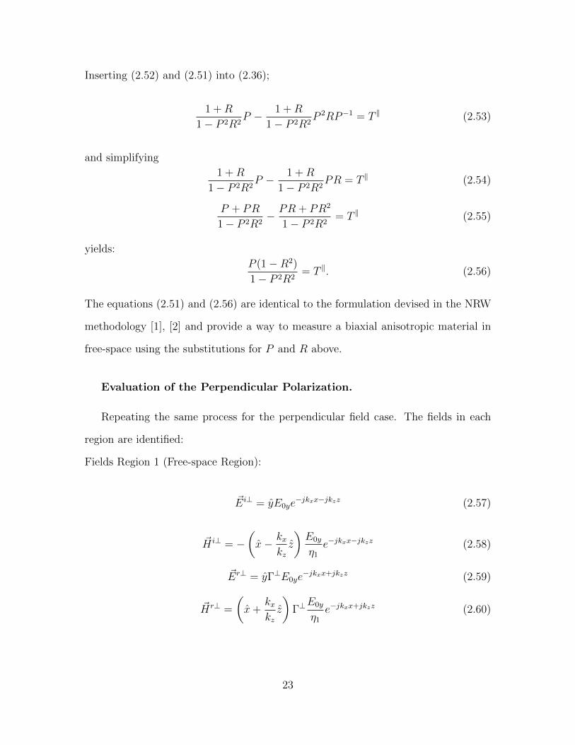
Inserting (2.52) and (2.51) into (2.36);
1 +R
1− P 2R2P − 1 +R
1− P 2R2P 2RP−1 = T ‖ (2.53)
and simplifying
1 +R
1− P 2R2P − 1 +R
1− P 2R2PR = T ‖ (2.54)
P + PR
1− P 2R2− PR + PR2
1− P 2R2= T ‖ (2.55)
yields:
P (1−R2)
1− P 2R2= T ‖. (2.56)
The equations (2.51) and (2.56) are identical to the formulation devised in the NRW
methodology [1], [2] and provide a way to measure a biaxial anisotropic material in
free-space using the substitutions for P and R above.
Evaluation of the Perpendicular Polarization.
Repeating the same process for the perpendicular field case. The fields in each
region are identified:
Fields Region 1 (Free-space Region):
~Ei⊥ = yE0ye−jkxx−jkzz (2.57)
~H i⊥ = −(x− kx
kzz
)E0y
η1
e−jkxx−jkzz (2.58)
~Er⊥ = yΓ⊥E0ye−jkxx+jkzz (2.59)
~Hr⊥ =
(x+
kxkzz
)Γ⊥
E0y
η1
e−jkxx+jkzz (2.60)
23

Fields Region 2 (Biaxial Anisotropic Slab):
~Et⊥ = yt⊥E0ye−jkxx−jk⊥z z (2.61)
~H t⊥ = −(x− µx
µz
kxk⊥zz
)t⊥E0y
η⊥2e−jkxx−jk
⊥z z (2.62)
~E1r⊥ = yΓ⊥1 E0ye−jkxx+jk⊥z z (2.63)
~H1r⊥ =
(x+
µxµz
kxk⊥zz
)Γ⊥1
E0y
η⊥2e−jkxx+jk⊥z z (2.64)
Fields Region 3 (Free-space Region):
~Et⊥ = yT⊥E0ye−jkxx−jkz(z−d) (2.65)
~H t⊥ = −(x− kx
kzz
)T⊥
E0y
η1
e−jkxx−jkz(z−d) (2.66)
Enforcing the continuity of tangential field boundary conditions at each interface
for the perpendicular polarization yields
Interface at z=0:
1 + Γ⊥ = t⊥ + Γ⊥1 (2.67)
1
η⊥1(1− Γ⊥) =
1
η⊥2(t⊥ − Γ⊥1 ) (2.68)
Interface at z=d:
t⊥e−jk⊥z z + Γ⊥1 e
jk⊥z z = T⊥ (2.69)
η1
η⊥2
(t⊥e−jk
⊥z z − Γ⊥1 e
jk⊥z z)
= T⊥ (2.70)
The equations that result by enforcing boundary conditions in the perpendicular case
are identical to the equation that are tangential at the interfaces of the parallel case.
Identifying that P = e−jk⊥z z, R =
η⊥2 −η1η⊥2 +η1
and simplifying yields equations for Γ⊥ and
24
T⊥, which are identical to (2.51) and (2.56).
Having these forms for both Γ‖, Γ⊥ and T ‖, T⊥ and their corresponding forms of
R‖, R⊥ and P ‖, P⊥ for each polarization keeps consistent with legacy material mea-
surement developments and shows a potential methodology for how a sample could
be measured. The transmission and reflection equations for the parallel and perpen-
dicular polarization forms developed in the forward formulation are then employed
in the inverse solution. The inverse solution is used for material sample measure-
ments. Calibrated sample transmission and reflection coefficient data are collected
and used as inputs to the inverse solution to provide permittivity and permeability
tensor elements.
2.5 Demonstration of Biaxial Anisotropic Slab Performance
Demonstrating the effects of a biaxial slab on transmitted and reflected electric
fields, MATLABr code is developed which solves for the transmission and reflection
coefficients for each polarization given a particular incident angle and permittivi-
ty/permeability tensor elements. The coefficients are then applied to their corre-
sponding electric field polarizations in both free-space regions 1 and 3. The electric
fields are then added together to provide the net polarization created by both paral-
lel and perpendicular polarized fields. The incident, transmitted and reflected fields
are plotted, demonstrating the polarization effects by the biaxial slab. Figure 6
demonstrates a slant 45 degree polarization electric field incident on a 0.9 inch thick
simulated biaxial anisotropic slab at an oblique incidence of 45 degrees that has the
25
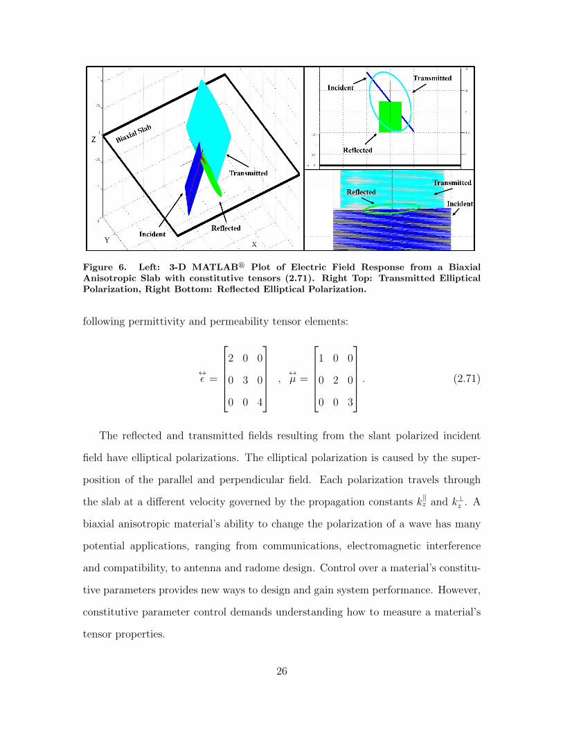
Figure 6. Left: 3-D MATLABr Plot of Electric Field Response from a BiaxialAnisotropic Slab with constitutive tensors (2.71). Right Top: Transmitted EllipticalPolarization, Right Bottom: Reflected Elliptical Polarization.
following permittivity and permeability tensor elements:
↔ε =
2 0 0
0 3 0
0 0 4
,↔µ =
1 0 0
0 2 0
0 0 3
. (2.71)
The reflected and transmitted fields resulting from the slant polarized incident
field have elliptical polarizations. The elliptical polarization is caused by the super-
position of the parallel and perpendicular field. Each polarization travels through
the slab at a different velocity governed by the propagation constants k‖z and k⊥z . A
biaxial anisotropic material’s ability to change the polarization of a wave has many
potential applications, ranging from communications, electromagnetic interference
and compatibility, to antenna and radome design. Control over a material’s constitu-
tive parameters provides new ways to design and gain system performance. However,
constitutive parameter control demands understanding how to measure a material’s
tensor properties.
26
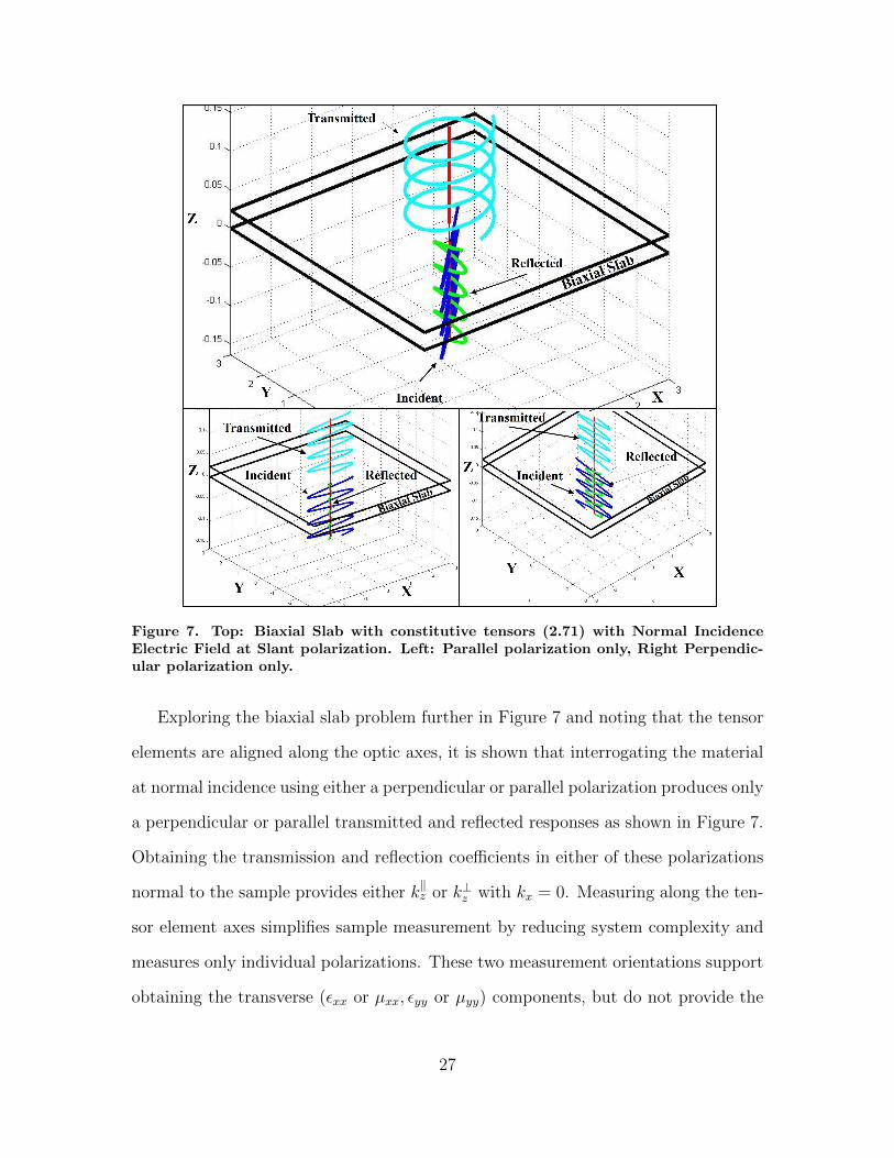
Figure 7. Top: Biaxial Slab with constitutive tensors (2.71) with Normal IncidenceElectric Field at Slant polarization. Left: Parallel polarization only, Right Perpendic-ular polarization only.
Exploring the biaxial slab problem further in Figure 7 and noting that the tensor
elements are aligned along the optic axes, it is shown that interrogating the material
at normal incidence using either a perpendicular or parallel polarization produces only
a perpendicular or parallel transmitted and reflected responses as shown in Figure 7.
Obtaining the transmission and reflection coefficients in either of these polarizations
normal to the sample provides either k‖z or k⊥z with kx = 0. Measuring along the ten-
sor element axes simplifies sample measurement by reducing system complexity and
measures only individual polarizations. These two measurement orientations support
obtaining the transverse (εxx or µxx, εyy or µyy) components, but do not provide the
27
longitudinal component (εzz or µzz). Measuring the longitudinal component would
require either an oblique incidence measurement (which increase measurement system
complexity to capture both polarizations) or indexing the sample to an orientation
where the longitudinal axis becomes the transverse axis and measuring it at normal
incidence.
2.6 Summary
The free-space analysis demonstrates the performance characteristics of a biaxial
material, which could be utilized in microwave systems to change the polarization of
incident waves with both vertical and horizontal polarizations. All permittivity and
permeability elements can be obtained by interrogating a sample at normal incidence
with respect to each tensor element. Evaluating the performance characteristics of a
biaxial anisotropic sample, evaluating a sample development technique and reviewing
waveguide measurement methods provides insight toward the development of a biaxial
anisotropic waveguide material measurement method.
28
III. Measurement Methodology
Characterization of a biaxial anisotropic material using waveguide techniques re-
quires a measurement apparatus that allows the sample to be index into different
orientations. The Waveguide Rectangular to Waveguide Square (WRWS) measure-
ment system supports the interrogation of a cubic sample by indexing it about its six
sides. The WRWS waveguide transitions are designed such that the gradual transi-
tions from a rectangular profile to square profile supports a TE10 mode of operation.
This gives the WRWS method two advantages over the previously mentioned mea-
surement techniques. The first advantage is the gradual transition supports a closed
form, analytic solution for extracting the constitutive parameters (↔ε ,↔µ). The second
advantage is the ability to utilize only 1 cubic sample and index it about its different
sides.
3.1 Waveguide Rectangular to Waveguide Square Development
The theoretical development for the WRWS system is a guided wave problem.
Unlike the TEM oblique incidence example in Chapter 2, the WRWS system has
additional boundary conditions which change the propagation constants and field
structure. It is shown that the WRWS system supports only the fundamental TE10
mode at X-band and the resulting equations from the forward problem development
take a form similar to the TEM wave problem. A conference paper [8] was presented
and published in conjunction with the development of this thesis. The conference
paper contains a short synopsis of the WRWS development and experimentation.
This section provides the same information presented in greater detail, to explicitly
demonstrate all parts of the WRWS theoretical development.
The TEM free-space development, demonstrated that constraint equations and
29
field relationships need to be identified to suit the forward problem development.
Extending the field analysis process, a source-free rectangular waveguide is assumed
completely filled with a biaxial anisotropic material and is infinite in extent. Evalu-
ating the source-free form of Maxwell’s Equations
∇× ~E = −jω↔µ · ~H, ∇× ~H = jω↔ε · ~E (3.1)
with the biaxial anisotropic tensors (2.4); it is determined that the curl equations
are y-invariant ( ∂∂y
= 0), because only the fundamental TE10 mode is present in the
WRWS waveguide due to the system operational frequency. This allows Maxwell’s
equations to be separated into two sets of modal equations: TEz and TMz. The TMz
modal equations will yield a trivial solution of zero and cannot exist in a y-invariant
structured environment. This dictates that only the TEz modal set :
∂Ey∂z
= jωµxHx,∂Ey∂x
= −jωµzHz (3.2)
and
∂Hz
∂x− ∂Hx
∂z= −jωεyEy (3.3)
will be present in the waveguide. Substituting the TEz field relations (3.2) into (3.3)
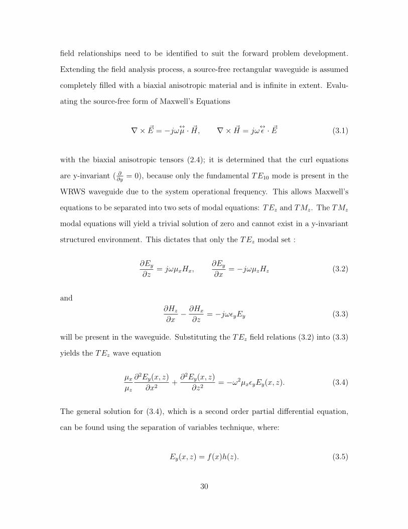
yields the TEz wave equation
µxµz
∂2Ey(x, z)
∂x2+∂2Ey(x, z)
∂z2= −ω2µxεyEy(x, z). (3.4)
The general solution for (3.4), which is a second order partial differential equation,
can be found using the separation of variables technique, where:
Ey(x, z) = f(x)h(z). (3.5)
30
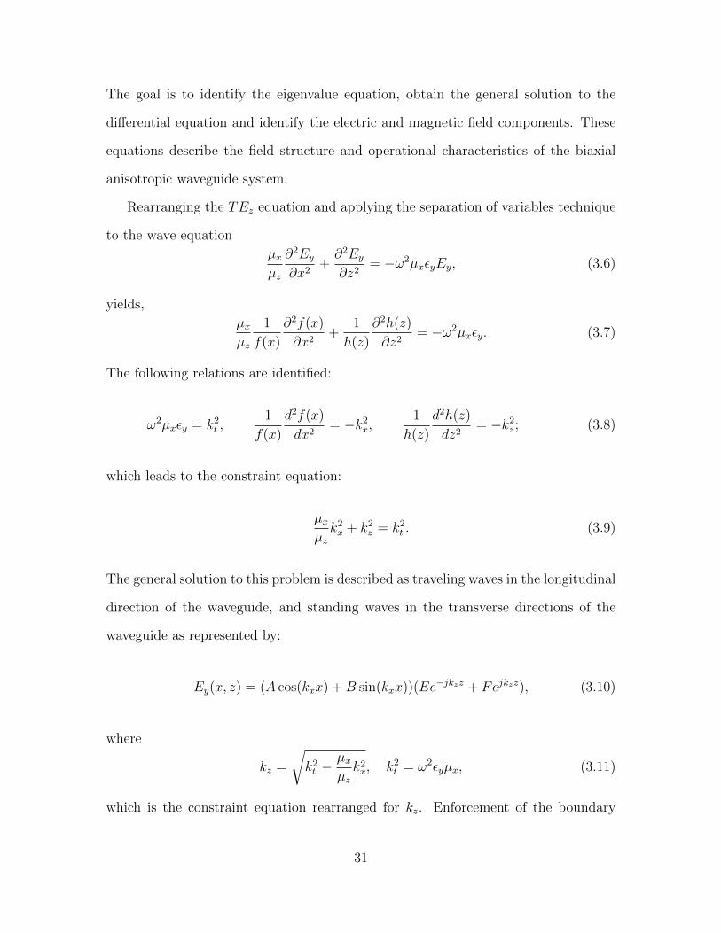
The goal is to identify the eigenvalue equation, obtain the general solution to the
differential equation and identify the electric and magnetic field components. These
equations describe the field structure and operational characteristics of the biaxial
anisotropic waveguide system.
Rearranging the TEz equation and applying the separation of variables technique
to the wave equation
µxµz
∂2Ey∂x2
+∂2Ey∂z2
= −ω2µxεyEy, (3.6)
yields,
µxµz
1
f(x)
∂2f(x)
∂x2+
1
h(z)
∂2h(z)
∂z2= −ω2µxεy. (3.7)
The following relations are identified:
ω2µxεy = k2t ,
1
f(x)
d2f(x)
dx2= −k2
x,1
h(z)
d2h(z)
dz2= −k2
z ; (3.8)
which leads to the constraint equation:
µxµzk2x + k2
z = k2t . (3.9)
The general solution to this problem is described as traveling waves in the longitudinal
direction of the waveguide, and standing waves in the transverse directions of the
waveguide as represented by:
Ey(x, z) = (A cos(kxx) +B sin(kxx))(Ee−jkzz + Fejkzz), (3.10)
where
kz =
√k2t −
µxµzk2x, k2
t = ω2εyµx, (3.11)
which is the constraint equation rearranged for kz. Enforcement of the boundary
31
conditions based on the waveguide’s geometry, as described in [11]:
Ey(x, z)|x=0,a= (A cos(kxx) +B sin(kxx))(Ee−jkzz + Fejkzz) = 0 (3.12)
leads to A = 0 when x = 0 and kx =mπ
awhen x = a; where m = 1, 2, 3 . . .∞, which
indicate the TEm0 modes of operation. Note that m 6= 0, this is a trivial solution.
Further reduction yields:
Ey(x, z) = (B sin(kxx))(Ee−jkzz + Fejkzz), (3.13)
and
Ey(x, z) = (sin(kxx))(BEe−jkzz +BFejkzz). (3.14)
The electric field general solution is constituted in terms of forward and reverse trav-
eling waves:
Ey(x, z) = (sin(kxx))(A+m0e
−jkzz + A−m0ejkzz) (3.15)
where A+m0 is the forward traveling wave amplitude and A−m0 is the reverse traveling
wave amplitude. Writing it more generally:
~E± = A±m0~em0e∓jkzz, where ~em0 = ysin(kxx). (3.16)
The transverse and longitudinal magnetic fields are then determined, once again,
similar to [11]:
Hx =1
jωµx
∂
∂z(sin(kxx)(A+
m0e−jkzz + A−m0e
jkzz)), (3.17)
32
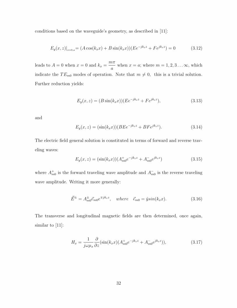
which evaluates to
Hx =−kzωµx
(sin(kxx)(A+m0e
−jkzz + A−m0ejkzz)). (3.18)
The wave impedance is defined as the ratio of the tangential electric field over the
tangential magnetic field for a single traveling wave, namely
ZTE = ∓E±yH±x
=ωµxkz
(3.19)
Thus, Hx is written as
Hx =−1
ZTE(sin(kxx)(A+
m0e−jkzz + A−m0e
jkzz)). (3.20)
The longitudinal magnetic field:
Hz =1
−jωµz∂
∂x(sin(kxx)(A+
m0e−jkzz + A−m0e
jkzz)), (3.21)
reduces to
Hz =−kxjωµz
(cos(kxx)(A+m0e
−jkzz + A−m0ejkzz)). (3.22)
The result of the biaxial anisotropic filled waveguide development yield similar
information as the TEM oblique incidence example and provides the wave impedance,
the constraint equation and information on how the waves propagate in the media
as well as the field structure. These components are used in the inverse solution
development of a biaxial filled sample region in the WRWS system.
33
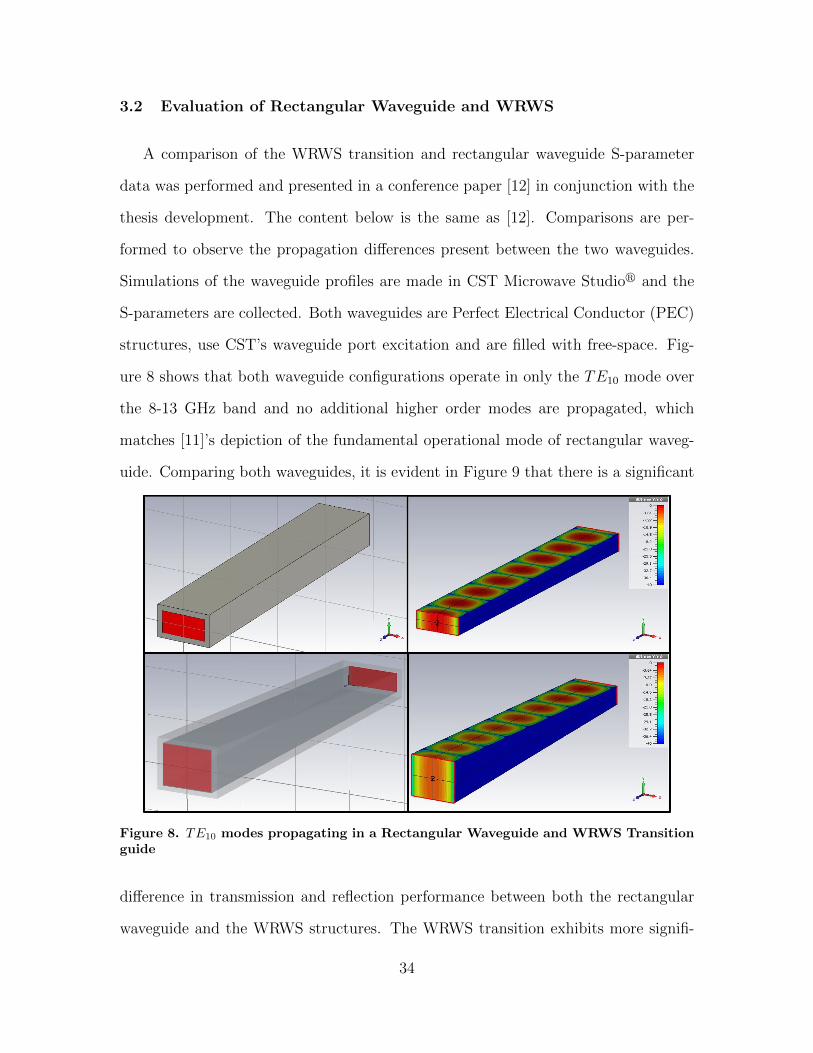
3.2 Evaluation of Rectangular Waveguide and WRWS
A comparison of the WRWS transition and rectangular waveguide S-parameter
data was performed and presented in a conference paper [12] in conjunction with the
thesis development. The content below is the same as [12]. Comparisons are per-
formed to observe the propagation differences present between the two waveguides.
Simulations of the waveguide profiles are made in CST Microwave Studior and the
S-parameters are collected. Both waveguides are Perfect Electrical Conductor (PEC)
structures, use CST’s waveguide port excitation and are filled with free-space. Fig-
ure 8 shows that both waveguide configurations operate in only the TE10 mode over
the 8-13 GHz band and no additional higher order modes are propagated, which
matches [11]’s depiction of the fundamental operational mode of rectangular waveg-
uide. Comparing both waveguides, it is evident in Figure 9 that there is a significant
Figure 8. TE10 modes propagating in a Rectangular Waveguide and WRWS Transitionguide
difference in transmission and reflection performance between both the rectangular
waveguide and the WRWS structures. The WRWS transition exhibits more signifi-
34

cant reflections than the rectangular waveguide and the power transmitted through
the WRWS transition has a greater sensitivity to the operational frequency. The
Figure 9. Comparison of Magnitude S-parameter Data: Top-Transmission, Bottom-Reflection
WRWS transition’s taper produces a magnitude response that is equivalent to a
series of waveguide apertures that have capacitive equivalent circuits [13]. The ca-
pacitance of the guide change in value as the aperture size changes over the length
of the guide. This causes the “scalloping” in both the transmitted and reflected
magnitude data in Figure 9. The differences in systematic responses between the
two waveguides, show that the guiding structure contributes a systematic response
to a material measurement. Removing this contribution, so it does not contaminate
the material measurement, requires a calibration technique. A TRL calibration (dis-
cussed in Chapter 4) is employed in both simulation and measurement to account for
the systematic responses of the WRWS and Rectangular Waveguide.
It is important to note that there are operational frequency limitations imposed
by the geometry change from rectangular to square. A rectangular waveguide cut-off
frequency at each mode is driven by the constraint equation and the material present
in the waveguide. Assuming a free space filled waveguide the cut-off frequencies for
each mode can be identified in [11] by
35

fc =1
2π√ε0µ0
√(mπa
)2
+(nπb
)2
(3.23)
where a and b are different dimensions and the modes are TEmn. A rectangular
waveguide has cut-off frequencies for the following modes as shown in the picture
in Figure 10 (Top Drawing) while a square waveguide exhibits the modal cut-off
Figure 10. Comparison of Modes Propagated versus Frequency: Top: RectangularWaveguide, Bottom: Square Waveguide
Figure 11. Waveguide arrangement
frequencies, shown in Figure 10 (Bottom Drawing). The square waveguide supports
modal excitation and propagation above TE10 at lower frequencies than a rectangular
waveguide. Having higher order modes at lower frequencies reduce the operational
36
bandwidth upon which materials can be characterized in closed form. Correcting the
bandwidth reduction problem requires a gradual WRWS transition and a length of
rectangular waveguide be installed on both sides of the WRWS setup as shown in
Figure 11, to insure that the TE01 and TE11 modes are suppressed. This allows for
material characterization to be performed using the WRWS over the full extent of
X-band without exciting the higher order modes. The operational bandwidth can be
extended higher in frequency if the TE20 is suppressed. A discussion of this observa-
tion is made in [14], and accomplished by exciting the waveguide with a symmetric
feed. This symmetric feed configuration is determined by the type of coax to waveg-
uide adapter used in the measurement set up.
3.3 Inverse Problem: Biaxial Parameter Extraction
This section provides the analysis of a y-invariant rectangular waveguide that has
only a local section uniformly filled (thus only a TE10 mode is present) with a biaxial
anisotropic material, as shown in Figure 12. This is different from the previous waveg-
uide field analysis because there are now three regions and two interfaces (similar to
the TEM analysis in Chapter 2). Once again, this development is also featured in
the conference paper [8], which was developed in conjunction with the development
of this thesis. These three regions have transmitted and reflected waves which are de-
scribed below. Region 1 is described by the following transverse forward and reverse
traveling waves:
~Et1 = a+1 ~em0e
−jkzz + a−1 ~em0ejkzz, (3.24)
~Ht1 = a+1~hm0e
−jkzz − a−1 ~hm0ejkzz. (3.25)
37
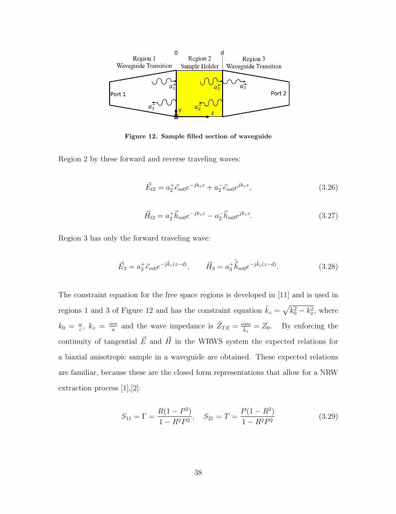
Figure 12. Sample filled section of waveguide
Region 2 by these forward and reverse traveling waves:
~Et2 = a+2 ~em0e
−jkzz + a−2 ~em0ejkzz, (3.26)
~Ht2 = a+2~hm0e
−jkzz − a−2 ~hm0ejkzz. (3.27)
Region 3 has only the forward traveling wave:
~E3 = a+3 ~em0e
−jkz(z−d), ~H3 = a+3~hm0e
−jkz(z−d). (3.28)
The constraint equation for the free space regions is developed in [11] and is used in
regions 1 and 3 of Figure 12 and has the constraint equation kz =√k2
0 − k2x, where
k0 = ωc, kx = mπ
aand the wave impedance is ZTE = ωµ0
kz= Z0. By enforcing the
continuity of tangential ~E and ~H in the WRWS system the expected relations for
a biaxial anisotropic sample in a waveguide are obtained. These expected relations
are familiar, because these are the closed form representations that allow for a NRW
extraction process [1],[2]:
S11 = Γ =R(1− P 2)
1−R2P 2, S21 = T =
P (1−R2)
1−R2P 2(3.29)
38
Unlike the traditional NRW method, the eigenvalue relations are different because the
sample is not isotropic. Therefore the biaxial anisotropic constraint equations (3.11)
are used to define the R and P terms of the material parameter extraction equations
(3.29). As shown in the conference paper [8] and also developed below, S-parameters
are collected at each orientation of the sample and correspond to values Rn and Pn,
where the subscript ‘n’ denotes the orientation of the sample as shown in Figure 13.
The reflection at the interface between the waveguide transition and the sample is
Rn =Zn − Z0
Zn + Z0
=Zn − 1
Zn + 1, (3.30)
where
Zn =Z
Z0
=ωµxkzn
kz0ωµ0
(3.31)
and is rearranged to represent
Zn =1 +Rn
1−Rn
. (3.32)
The transmission through the sample is described by
Pn = e−jkznd, (3.33)
and is rearranged to obtain
j lnPnd
= kzn. (3.34)
Once Zn and kzn are obtained, the transverse permeability component can be
determined from
µxn =Znkznµ0
kz0. (3.35)
Using the transverse permeability µxn, the transverse permittivity εyn can be solved
39

Figure 13. Unit Cell Cubic Sample
by rearranging (3.11) into the form
εyn =k2zn + µxn
µzk2x
ω2µxn(3.36)
where µz is the permeability found from a separate transverse permeability measure-
ment of the sample indexed in a different orientation.
Evaluating a cubic sample about the 6 orientations, as shown in Figure 13, will
yield a pair of permittivity and permeability tensors in x, y and z. Permittivity in
y is calculated from orientations 1 and 2; x from orientations 5 and 6; and z from
orientations 3 and 4. Permeability in x is computed from orientations 2 and 6; y from
orientations 4 and 5; and z from orientations 1 and 3 as shown in Figure 13.
40
Using the sample orientations of Figure 13 in conjunction with the equations (3.35)
and (3.36) yields
µ1 =Z1kz1µ0
kz0, ε1 =
k2z1 + µ1
µ2k2x
ω2µ1
(3.37)
µ2 =Z2kz2µ0
kz0, ε2 =
k2z2 + µ2
µ1k2x
ω2µ2
(3.38)
µ3 =Z3kz3µ0
kz0, ε3 =
k2z3 + µ3
µ4k2x
ω2µ3
(3.39)
µ4 =Z4kz4µ0
kz0, ε4 =
k2z4 + µ4
µ3k2x
ω2µ4
(3.40)
µ5 =Z5kz5µ0
kz0, ε5 =
k2z5 + µ5
µ6k2x
ω2µ5
(3.41)
µ6 =Z6kz6µ0
kz0, ε6 =
k2z6 + µ6
µ5k2x
ω2µ6
(3.42)
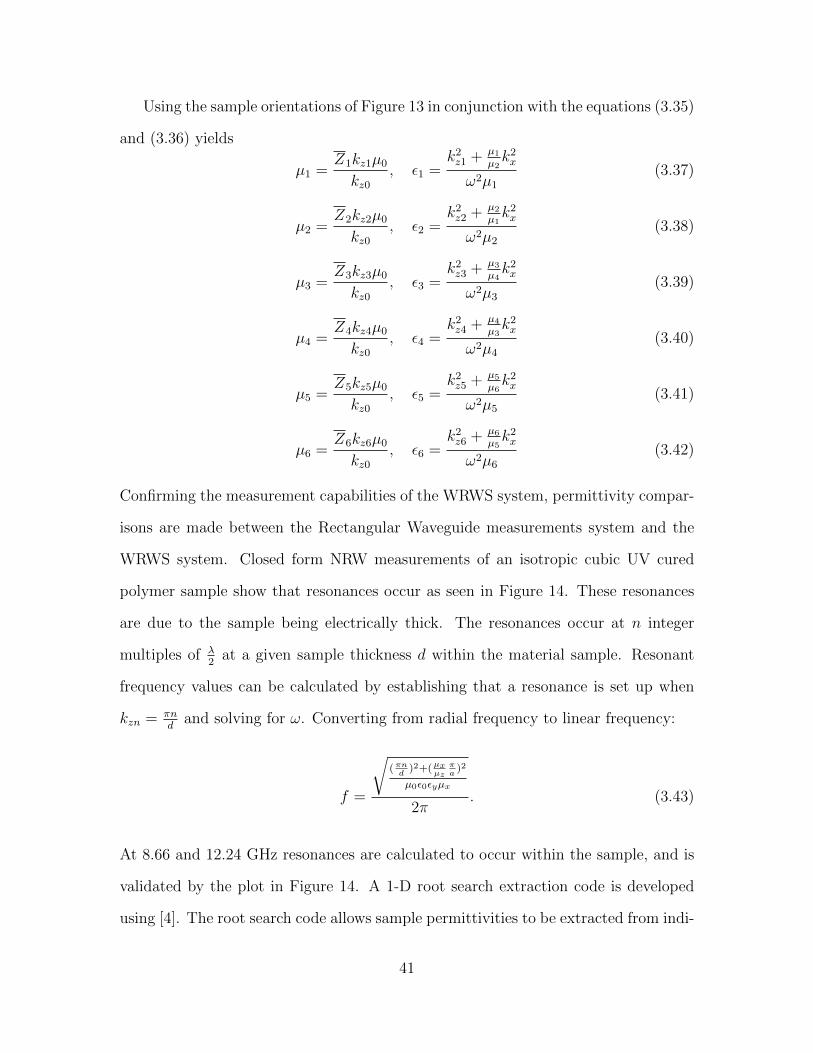
Confirming the measurement capabilities of the WRWS system, permittivity compar-
isons are made between the Rectangular Waveguide measurements system and the
WRWS system. Closed form NRW measurements of an isotropic cubic UV cured
polymer sample show that resonances occur as seen in Figure 14. These resonances
are due to the sample being electrically thick. The resonances occur at n integer
multiples of λ2
at a given sample thickness d within the material sample. Resonant
frequency values can be calculated by establishing that a resonance is set up when
kzn = πnd
and solving for ω. Converting from radial frequency to linear frequency:
f =
√(πnd
)2+(µxµz
πa
)2
µ0ε0εyµx
2π. (3.43)
At 8.66 and 12.24 GHz resonances are calculated to occur within the sample, and is
validated by the plot in Figure 14. A 1-D root search extraction code is developed
using [4]. The root search code allows sample permittivities to be extracted from indi-
41
Figure 14. Closed form measurement with sample resonances at nλ2
vidual S-parameters, and avoid the resonance issue, assuming that the permeability
is known (µ = µ0 in this case). A performance comparison measurement is made
between the rectangular waveguide (RWG) measurement technique and the WRWS
system. The RWG and WRWS sample holders are measured empty, to measure the
air occupying the volume. This measurement eliminates the potential variability of
the sample and has a expected relative permittivity of εr = 1. The comparison shows
excellent agreement between the RWG and WRWS measurement systems as seen
in Figure 15. Based on the recommendations in [4] and observing the stability of
the extracted root search results in Figure 15, the S21 data is used as the primary
S-parameter data source for the 1-D root search material parameter extraction. A
rectangular sample of UV cured polymer and a cube sample of UV cured polymer,
shown in Figure 16 are developed to support the measurements. It is shown that
the UV cured polymer materials measures at εr ≈ 2.8655 − 0.04j at mid-band, as
seen in Figure 17, and used as the permittivity value for the UV cured polymer in all
prediction models.
42

Figure 15. Comparison of RWG and WRWS with Free-space filled sample holder: Left:S11, Right: S21
3.4 Summary
The measurement comparisons between isotropic sample shows that the devel-
oped closed form biaxial anisotropic NRW-type formulation for material parameter
extraction yields identical results to the legacy RWG method. Additionally, it is also
shown that higher order modes are not excited by the WRWS transitions. Success-
ful isotropic testing of the WRWS measurement methodology provides confidence in
anisotropic sample development, prediction and testing.
43

Figure 16. Isotropic UV cured RWG (Top) and WRWS (Bottom) polymer samplesand sample holders
44
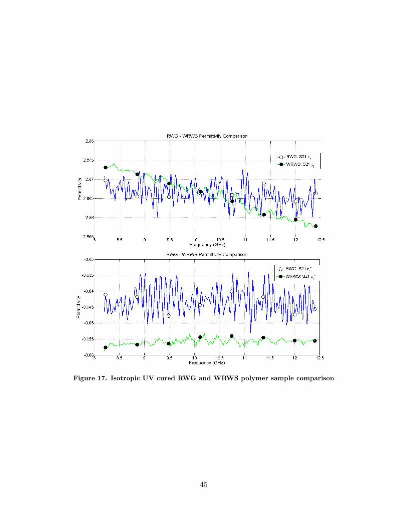
Figure 17. Isotropic UV cured RWG and WRWS polymer sample comparison
45
IV. Sample Development
Testing the WRWS system’s anisotropic measurement abilities requires that a
sample be constructed which possesses biaxial anisotropic constitutive parameters.
A sample geometry is designed using crystallographic symmetry and manufactured
using a UV cured 3-D polymer printer. Two prediction capabilities are devised to
support the sample design: A lumped element equivalent circuit approach and a CEM
Frequency Domain model in CST Microwave Studior.
4.1 Biaxial Sample Development
Dmitriev [10] shows that different electromagnetic performance capabilities can be
designed using crystallographic symmetry. 3-D geometric shapes exhibit various forms
of rotational and axial symmetry. Curie’s and Neumann’s Principles [10] provide
the mathematical development for combining shapes and symmetries. New, more
complex shapes can be made from combinations of different primitive crystals.
The WRWS system accommodates cubic samples, which imposes the requirement
that the parent structure must be a cube. Review of Collin’s paper [9] shows a po-
tential arrangement for rectangular inclusions yielding biaxial performance. These
rectangular inclusions are orthorhombic unit cells. Arranging orthorhombic crystals
inside a cubic structure suggests that the arrangement be orthorhombic as well, max-
imizing the utilization of cubic volume. Showing the mathematical development for
Collin’s design, Dmitriev’s crystal groups and the International Tables for Crystal-
lography [15],[16] notation provide the crystallographic design and demonstrates that
the resulting geometry yields an electromagnetic biaxial anisotropic sample design,
as seen in Figure 18. Curie’s principle
↔ε = [inclusion symmetry] ∩ [arrangement symmetry] ∩ [cube symmetry] (4.44)
46
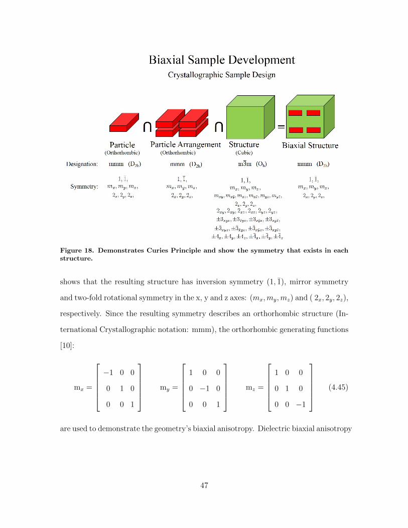
Figure 18. Demonstrates Curies Principle and show the symmetry that exists in eachstructure.
shows that the resulting structure has inversion symmetry (1, 1), mirror symmetry
and two-fold rotational symmetry in the x, y and z axes: (mx,my,mz) and ( 2x, 2y, 2z),
respectively. Since the resulting symmetry describes an orthorhombic structure (In-
ternational Crystallographic notation: mmm), the orthorhombic generating functions
[10]:
mx =
−1 0 0
0 1 0
0 0 1
my =
1 0 0
0 −1 0
0 0 1
mz =
1 0 0
0 1 0
0 0 −1
(4.45)
are used to demonstrate the geometry’s biaxial anisotropy. Dielectric biaxial anisotropy
47
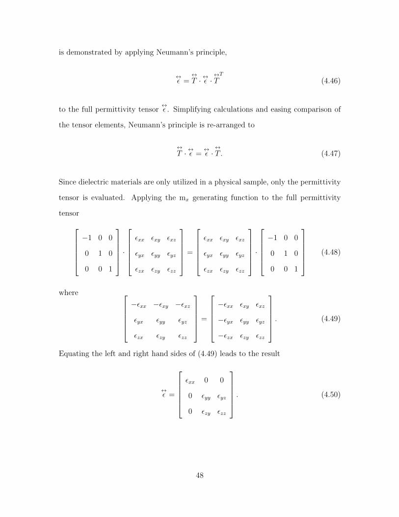
is demonstrated by applying Neumann’s principle,
↔ε =
↔T · ↔ε ·
↔TT
(4.46)
to the full permittivity tensor↔ε . Simplifying calculations and easing comparison of
the tensor elements, Neumann’s principle is re-arranged to
↔T · ↔ε =
↔ε ·↔T . (4.47)
Since dielectric materials are only utilized in a physical sample, only the permittivity
tensor is evaluated. Applying the mx generating function to the full permittivity
tensor−1 0 0
0 1 0
0 0 1
·εxx εxy εxz
εyx εyy εyz
εzx εzy εzz
=
εxx εxy εxz
εyx εyy εyz
εzx εzy εzz
·−1 0 0
0 1 0
0 0 1
(4.48)
where −εxx −εxy −εxz
εyx εyy εyz
εzx εzy εzz
=
−εxx εxy εxz
−εyx εyy εyz
−εzx εzy εzz
. (4.49)
Equating the left and right hand sides of (4.49) leads to the result
↔ε =
εxx 0 0
0 εyy εyz
0 εzy εzz
. (4.50)
48

Applying my to the solution (4.50):
1 0 0
0 −1 0
0 0 1
·εxx 0 0
0 εyy εyz
0 εzy εzz
=
εxx 0 0
0 εyy εyz
0 εzy εzz
·
1 0 0
0 −1 0
0 0 1
(4.51)
where εxx 0 0
0 −εyy −εyz
0 εzy εzz
=
εxx 0 0
0 −εyy εyz
0 −εzy εzz
. (4.52)
Equating the left and right hand sides of (4.52) leads to the result
↔ε =
εxx 0 0
0 εyy 0
0 0 εzz
. (4.53)
Applying the remaining generating function mz:1 0 0
0 1 0
0 0 −1
·εxx 0 0
0 εyy 0
0 0 εzz
=
εxx 0 0
0 εyy 0
0 0 εzz
·
1 0 0
0 1 0
0 0 −1
(4.54)
where εxx 0 0
0 εyy 0
0 0 −εzz
=
εxx 0 0
0 εyy 0
0 0 −εzz
. (4.55)
Equating the left and right hand sides of (4.55) does not reveal any additional in-
formation regarding the tensor structure. The resulting permittivity tensor (4.53)
demonstrates that the biaxial structure featured in Figure 18 has three unique di-
49
agonal elements, assuming tensor alignment along the optic axis. Crystallographic
symmetry provides structural guidance on how to design a biaxial anisotropic sample,
but does not provide information for specific tensor element values or exact sample
dimensions.
4.2 Lumped Element Prediction of Biaxial Anisotropic Constitutive Pa-
rameters
Prediction of biaxial anisotropic constitutive parameters is important to the design
and synthesis of a testable material. Additionally, prediction methods provide com-
parison data, which can be compared to measured experimental results. A lumped
element equivalent circuit prediction method is used to provide estimations on bi-
axial anisotropic tensor values. Biaxial sample design factors include the number
of cells (inclusions or occlusions), cell dimensions and the materials used. Electric
Capacitance [17] and Magnetic Inductance [18] equations,
C =εrε0S
d, L =
d
µrµ0S, (4.56)
where S is the surface area and d is the gap distance for the representative equivalent
circuit component, serve as models and describe each piece of a sample, as seen in
Figure 19. The lumped element model relates the sample’s structural dimensions and
materials to a circuit equivalent network which provides an approximation of the sam-
ple’s permittivity or permeability. Depending on how the sample is discretized into
circuit components and which sample measurement orientation is evaluated, different
sample constitutive tensor element values are obtained.
50
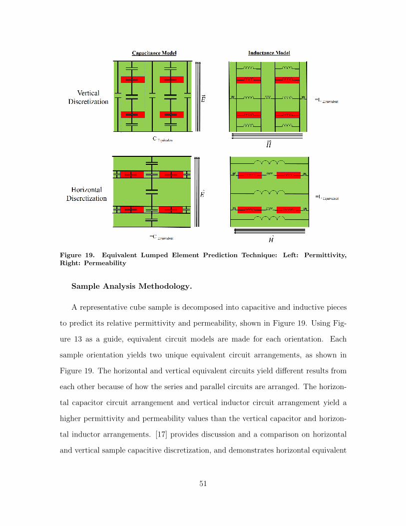
Figure 19. Equivalent Lumped Element Prediction Technique: Left: Permittivity,Right: Permeability
Sample Analysis Methodology.
A representative cube sample is decomposed into capacitive and inductive pieces
to predict its relative permittivity and permeability, shown in Figure 19. Using Fig-
ure 13 as a guide, equivalent circuit models are made for each orientation. Each
sample orientation yields two unique equivalent circuit arrangements, as shown in
Figure 19. The horizontal and vertical equivalent circuits yield different results from
each other because of how the series and parallel circuits are arranged. The horizon-
tal capacitor circuit arrangement and vertical inductor circuit arrangement yield a
higher permittivity and permeability values than the vertical capacitor and horizon-
tal inductor arrangements. [17] provides discussion and a comparison on horizontal
and vertical sample capacitive discretization, and demonstrates horizontal equivalent
51
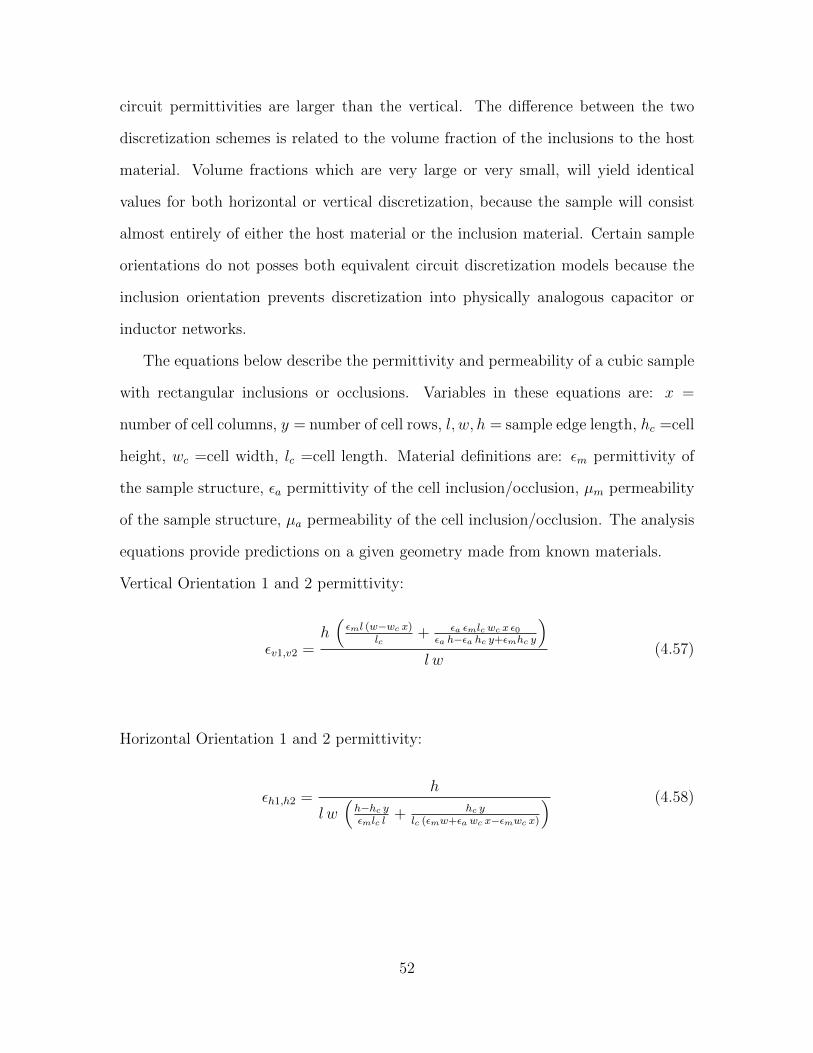
circuit permittivities are larger than the vertical. The difference between the two
discretization schemes is related to the volume fraction of the inclusions to the host
material. Volume fractions which are very large or very small, will yield identical
values for both horizontal or vertical discretization, because the sample will consist
almost entirely of either the host material or the inclusion material. Certain sample
orientations do not posses both equivalent circuit discretization models because the
inclusion orientation prevents discretization into physically analogous capacitor or
inductor networks.
The equations below describe the permittivity and permeability of a cubic sample
with rectangular inclusions or occlusions. Variables in these equations are: x =
number of cell columns, y = number of cell rows, l, w, h = sample edge length, hc =cell
height, wc =cell width, lc =cell length. Material definitions are: εm permittivity of
the sample structure, εa permittivity of the cell inclusion/occlusion, µm permeability
of the sample structure, µa permeability of the cell inclusion/occlusion. The analysis
equations provide predictions on a given geometry made from known materials.
Vertical Orientation 1 and 2 permittivity:
εv1,v2 =h(εml (w−wc x)
lc+ εa εmlc wc x ε0
εa h−εa hc y+εmhc y
)l w
(4.57)
Horizontal Orientation 1 and 2 permittivity:
εh1,h2 =h
l w(h−hc yεmlc l
+ hc ylc (εmw+εa wc x−εmwc x)
) (4.58)
52
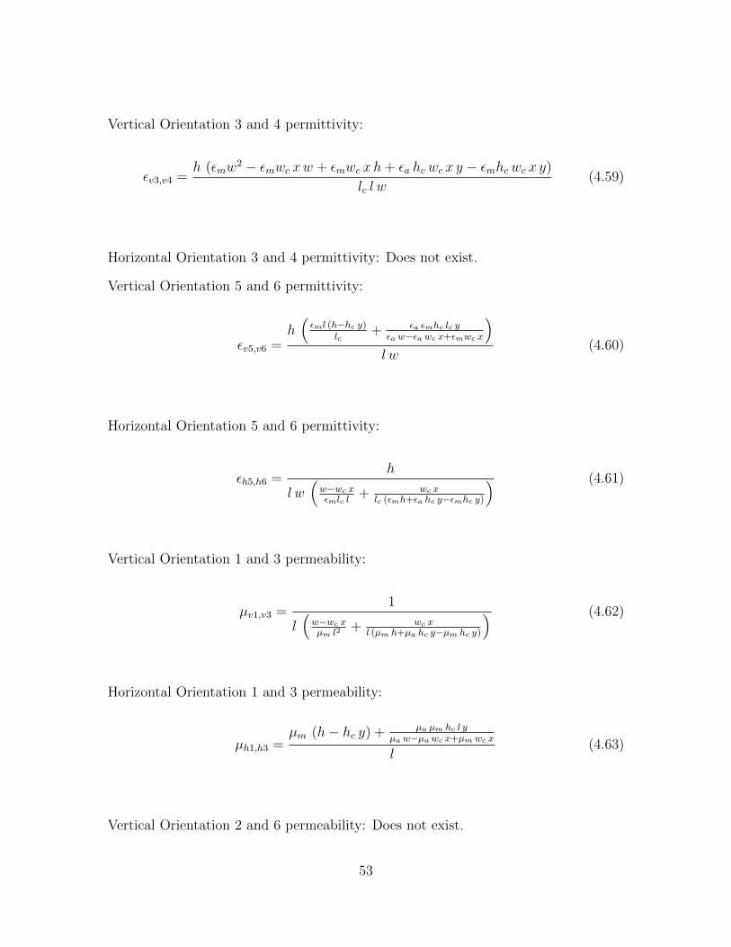
Vertical Orientation 3 and 4 permittivity:
εv3,v4 =h (εmw
2 − εmwc xw + εmwc xh+ εa hcwc x y − εmhcwc x y)
lc l w(4.59)
Horizontal Orientation 3 and 4 permittivity: Does not exist.
Vertical Orientation 5 and 6 permittivity:
εv5,v6 =h(εml (h−hc y)
lc+ εa εmhc lc y
εa w−εa wc x+εmwc x
)l w
(4.60)
Horizontal Orientation 5 and 6 permittivity:
εh5,h6 =h
l w(w−wc xεmlc l
+ wc xlc (εmh+εa hc y−εmhc y)
) (4.61)
Vertical Orientation 1 and 3 permeability:
µv1,v3 =1
l(w−wc xµm l2
+ wc xl (µm h+µa hc y−µm hc y)
) (4.62)
Horizontal Orientation 1 and 3 permeability:
µh1,h3 =µm (h− hc y) + µa µm hc l y
µa w−µa wc x+µm wc x
l(4.63)
Vertical Orientation 2 and 6 permeability: Does not exist.
53
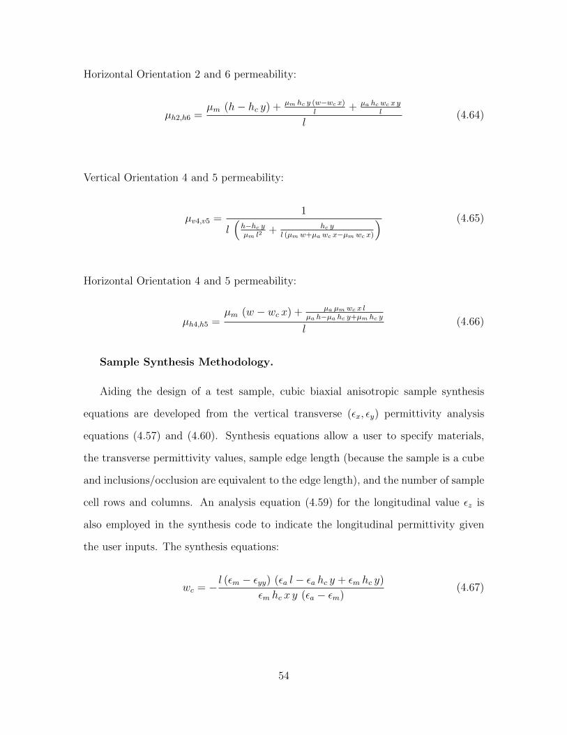
Horizontal Orientation 2 and 6 permeability:
µh2,h6 =µm (h− hc y) + µm hc y (w−wc x)
l+ µa hc wc x y
l
l(4.64)
Vertical Orientation 4 and 5 permeability:
µv4,v5 =1
l(h−hc yµm l2
+ hc yl (µm w+µa wc x−µm wc x)
) (4.65)
Horizontal Orientation 4 and 5 permeability:
µh4,h5 =µm (w − wc x) + µa µm wc x l
µa h−µa hc y+µm hc y
l(4.66)
Sample Synthesis Methodology.
Aiding the design of a test sample, cubic biaxial anisotropic sample synthesis
equations are developed from the vertical transverse (εx, εy) permittivity analysis
equations (4.57) and (4.60). Synthesis equations allow a user to specify materials,
the transverse permittivity values, sample edge length (because the sample is a cube
and inclusions/occlusion are equivalent to the edge length), and the number of sample
cell rows and columns. An analysis equation (4.59) for the longitudinal value εz is
also employed in the synthesis code to indicate the longitudinal permittivity given
the user inputs. The synthesis equations:
wc = − l (εm − εyy) (εa l − εa hc y + εm hc y)
εm hc x y (εa − εm)(4.67)
54

and
hc = − l (εm − εxx) (εa l − εawc x+ εmwc x)
εmwc x y (εa − εm)(4.68)
outputs describe the cell (inclusion/occlusion) dimensions. The output dimensions of
the synthesis equations are then used to construct the sample in a CAD utility. The
resulting CAD file is then printed on a UV cured polymer 3-D printer.
Figure 20. Sample and Sample Holder
MATLABr code is written to utilize both the analysis and synthesis equations.
The synthesis code is used to generate a cubic sample with air occlusions because
the 3-D printer can only print one material. The goal is to have the sample’s relative
permittivity values spread as far apart as possible to maximize biaxial anisotropic
performance. Tensor element values are, however, constrained by the sample’s par-
ent materials, air εr = 1 and the UV cured polymer εr ≈ 2.86, which establish a
lower and upper bound to the permittivity. Sample design factors include: main-
taining macroscopic EM averaging, sample robustness and ease of printing. Each of
these factors create trade-space in the sample design. Multiple occlusions of small
dimension should be used to maintain macroscopic EM, while fewer inclusions with
larger cell dimensions provide for a more structurally robust sample, and is more
easily printed. Accommodating these design factors and maximizing the spread in
biaxial permittivity leads to the sample design featured in Figure 13, verified using
the lumped element analysis code, printed on a UV cured 3-D polymer printer and
55
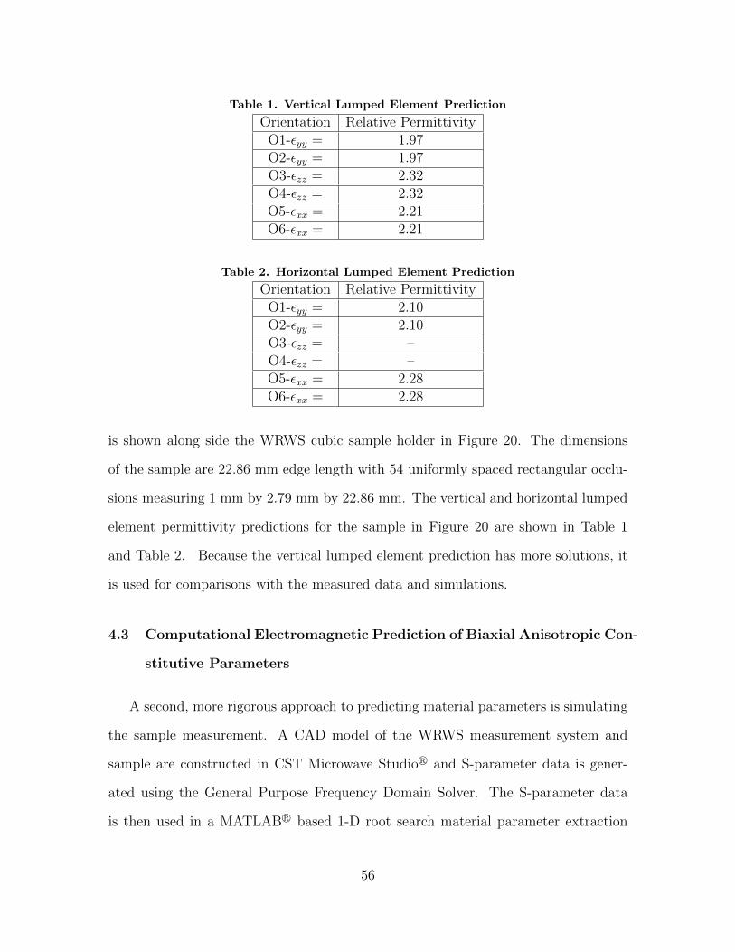
Table 1. Vertical Lumped Element Prediction
Orientation Relative PermittivityO1-εyy = 1.97O2-εyy = 1.97O3-εzz = 2.32O4-εzz = 2.32O5-εxx = 2.21O6-εxx = 2.21
Table 2. Horizontal Lumped Element Prediction
Orientation Relative PermittivityO1-εyy = 2.10O2-εyy = 2.10O3-εzz = –O4-εzz = –O5-εxx = 2.28O6-εxx = 2.28
is shown along side the WRWS cubic sample holder in Figure 20. The dimensions
of the sample are 22.86 mm edge length with 54 uniformly spaced rectangular occlu-
sions measuring 1 mm by 2.79 mm by 22.86 mm. The vertical and horizontal lumped
element permittivity predictions for the sample in Figure 20 are shown in Table 1
and Table 2. Because the vertical lumped element prediction has more solutions, it
is used for comparisons with the measured data and simulations.
4.3 Computational Electromagnetic Prediction of Biaxial Anisotropic Con-
stitutive Parameters
A second, more rigorous approach to predicting material parameters is simulating
the sample measurement. A CAD model of the WRWS measurement system and
sample are constructed in CST Microwave Studior and S-parameter data is gener-
ated using the General Purpose Frequency Domain Solver. The S-parameter data
is then used in a MATLABr based 1-D root search material parameter extraction
56

code to calculate permittivity values. The work presented here is also presented in a
conference paper [12], in conjunction with the development of this thesis.
Initially, it was assumed that CST Microwave Studior performed a calibrated
de-embed on the material measurements. The material sample S-parameter data was
de-embedded from the model using CST’s waveguide port “Distance to ref. plane”
function [19]. However, it was observed, in simulations of known isotropic sam-
ples, extracted WRWS permittivity data exhibited significant non-physical frequency
dispersion and did not agree with expected results. A diagnostic comparison was
performed to evaluate the differences between a rectangular waveguide and WRWS
material parameter extraction model in CST. A 4.13 mm thick sample of an isotropic
Teflonr εr = 2.1− j0.0004 was simulated as seen in Figure 21 and results were com-
Figure 21. CST models of Rectangular Waveguide and WRWS system (Left), TeflonSamples installed (Right)
pared as seen in Figure 22. Both models utilize CST’s waveguide port “Distance to
ref. plane” function to de-embed the S-parameters used to obtain the extracted per-
mittivities. It is observed in Figure 22 that the results do not match the permittivity
57

of Teflonr, and the WRWS results exhibit significant ripple due to the reflections
caused by the WRWS’s tapered transitions, as observed in Figure 9. Additionally,
the extracted rectangular waveguide permittivity data is not exactly the permittivity
value of Teflonr. Based on the results, it is observed that systematic errors associ-
ated with the waveguide transitions distort the extracted WRWS permittivity results,
similar to how the results would be effected in a poorly calibrated material sample
measurement.
Figure 22. CST WRWS Teflon Sample De-embedded
58
Simulation calibration and sample measurement.
Material measurement/simulation performance can be degraded by systematic
errors. These systematic errors include the reflections created by transitions or mis-
matches in waveguide, cable-connectors, or devices. Network Analyzers can com-
pensate for these systematic errors by measuring their own receiver amplitude and
phase sensitivities and using calibration routines to remove reflection/transmission
errors. The Thru-Reflect-Line (TRL) calibration technique described by [20] removes
these systematic errors and mathematically establishes reference planes at the lo-
cation where the TRL calibration technique is applied. A TRL calibration process
is employed in CST Microwave Studior to remove systematic errors from both the
WRWS and rectangular waveguide simulated measurements. Simulated CST data is
then used in a TRL calibration code that was written in MATLABr based on the
work of [20] and Doug Rytting’s technical papers [21] , [22]. The TRL calibration code
is used for both experimentally measured and simulated material measurements and
is mathematically described below. Differences between simulated TRL calibrations
and measured are in the assumption of a perfectly matched receivers in simulated
data, and imperfect receivers, which are measured and accounted for in experimental
data. Receiver accountability is described as:
s11 =sraw11 − sraw12
R2R1
1− R2R1
R1R2
(4.69)
s12 =sraw12 − sraw11
R2R1
1− R2R1
R1R2
(4.70)
s21 =sraw21 − sraw22
R1R2
1− R1R2
R2R1
(4.71)
s22 =sraw22 − sraw21
R1R2
1− R1R2
R2R1
(4.72)
59

where R1R2
andR2R1
are the port receiver ratios and may not be reciprocal or equivalent.
S-parameter data denoted by “raw” is the data uncalibrated, un-ratioed data from
the VNA. Four total measurements (Thru, Reflect, Line and Sample) are required to
produce calibrated data as shown in Figure 23. Because of these four measurements,
four separate CST simulations (one for each measurement: Thru, Reflect, Line and
Sample) are made and 2-port S-parameter data is collected from each simulation.
Network Analysis T-parameters
Figure 23. Graphical Depiction of TRL calibration
t11 t12
t21 t22
=1
s21
s21s12 − s11s22 s11
−s22 1
(4.73)
are used to describe each of the components in the waveguide measurement system
and mathematically links them together. Doug Rytting in [22] demonstrates the de-
60
velopment and relationship between T-parameters and S-parameters. The [X] matrix
describes the left tapered transition; [Y ] matrix the right tapered transition and [U ]
matrix the sample region or material under test (MUT) as depicted in Figure 23. The
thru and line measurements are used to calculate the [X] and [Y ] as represented by
[M ] = [T ]line[T ]−1thru [N ] = [T ]−1
thru[T ]line. (4.74)
and
[M ][X] = [X][T ]line [Y ][N ] = [T ]line[Y ]. (4.75)
Solving for [X] and [Y ] requires rearranging (4.75) and solving the system of equa-
tions. The rearranged equations are quadratic and each pose two potential solutions.
The [X] can be evaluated by
x11
x21
,x12
x22
=(m11 −m22)±
√(m11 −m22)2 + 4m21m12
2m21
(4.76)
and [Y ] by
y11
y12
,y21
y22
=(n11 − n22)±
√(n11 − n22)2 + 4n21n12
2n12
. (4.77)
The root choices are made as such, if∣∣∣x11x21
∣∣∣ > ∣∣∣x12x22
∣∣∣ then a = x11x21
and b = x12x22
else
b = x11x21
and a = x12x22
, sx11 = b. Likewise, if∣∣∣y11y12
∣∣∣ > ∣∣∣y21y22
∣∣∣ then c = y11y12
and d = y21y22
else
d = y11y12
and c = y21y22
, sy22 = −d. These root choices represent a decision as to which
components are transmitted and reflected. The assumption is that in most passive
devices the power reflected is less than the power transmitted. Isolating sx22 utilizes
the reflection measurement and requires a root choice be made as applied to the form
sx22 = ±
√(st11 − b)(sr11 − b)(sr22 + c)
(st11 − a)(sr11 − a)(sr22 + d). (4.78)
61

The reflect measurement is also used to solve for the remaining terms of the equation
Γr =sr11 − b
sx22(sr11 − a). (4.79)
Because sx22 has two possible roots, a root choice must be made to select the correct
choice of sx22 such that Γr < 0. Using the solutions and measurements provided above,
the remaining equations are solved:
sy11 =st11 − b
sx22(sr11 − a)(4.80)
sx21sy21 = st21(1− sx22s
y11) (4.81)
sy21sy12 = sy11(c− d) (4.82)
sx21sx12 = sx11(b− a) (4.83)
Once all of the terms are solved then they can be applied to the [X] and [Y ] matrices:
y11 y12
y21 y22
=
sy21sy12 − s
y11s
y22 sy11
−sy22 1
(4.84)
x11 x12
x21 x22
=
sx21sx12 − sx11s
x22 sx11
−sx22 1
. (4.85)
The sample measurement data is then applied and the waveguide structure is math-
ematically removed by
[T ]u = sx21sy21[X]−1[T ]MUT [Y ]−1 (4.86)
62
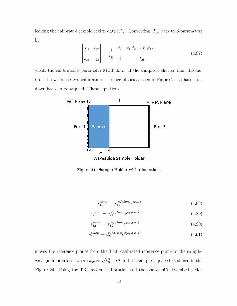
leaving the calibrated sample region data [T ]u. Converting [T ]u back to S-parameters
by s11 s12
s21 s22
=1
t22
t21 t11t22 − t21t12
1 −t21
(4.87)
yields the calibrated S-parameter MUT data. If the sample is shorter than the dis-
tance between the two calibration reference planes as seen in Figure 24 a phase shift
de-embed can be applied. These equations:
Figure 24. Sample Holder with dimensions
ssamp.11 = sref.plane11 ejkz00 (4.88)
ssamp.21 = sref.plane21 ejkz0(w−l) (4.89)
ssamp.12 = sref.plane12 ejkz0(w−l) (4.90)
ssamp.22 = sref.plane22 e2jkz0(w−l) (4.91)
moves the reference planes from the TRL calibrated reference plane to the sample-
waveguide interface, where kz0 =√k2
0 − k2x and the sample is placed as shown in the
Figure 24. Using the TRL system calibration and the phase-shift de-embed yields
63
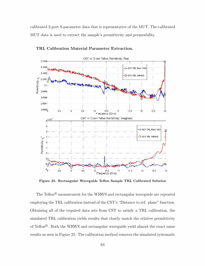
calibrated 2-port S-parameter data that is representative of the MUT. The calibrated
MUT data is used to extract the sample’s permittivity and permeability.
TRL Calibration Material Parameter Extraction.
Figure 25. Rectangular Waveguide Teflon Sample TRL Calibrated Solution
The Teflonr measurement for the WRWS and rectangular waveguide are repeated
employing the TRL calibration instead of the CST’s “Distance to ref. plane” function.
Obtaining all of the required data sets from CST to satisfy a TRL calibration, the
simulated TRL calibration yields results that closely match the relative permittivity
of Teflonr. Both the WRWS and rectangular waveguide yield almost the exact same
results as seen in Figure 25. The calibration method removes the simulated systematic
64

errors and provides data that matches expected permittivity values.
4.4 Summary
Two prediction methods have been developed to support sample design and WRWS
testing. The lumped element methodology provides permittivity and permeability
tensor data and a sample design, while the CEM analysis in CST provides a sim-
ulated and calibrated measurement environment to evaluate the designed sample’s
performance. The simulated results can be compared with experimentally measured
data to validate WRWS system performance and demonstrate the lumped element
designed sample.
65

V. Results
Biaxial anisotropic material measurement test data is collected using the WRWS
measurement system. The results are compared to the lumped element and CST
Microwave Studior predictions. A Monte Carlo uncertainty analysis is performed on
the test data. Comparisons between prediction methods and physical experiments
demonstrate WRWS measurement capability effectiveness.
Figure 26. WRWS setup and view of square aperture
5.1 The WRWS system
The WRWS system is constructed from 6010 Aluminum stock. WRWS transitions,
0.9” cubic sample holder and 0.4” thick square aperture calibration line standard
profiles, shown in Figures 26 and 27, are cut using a wire electrical discharge machine
(EDM). The WRWS system uses the WR-90 precision alignment flange pattern for
system assembly. WRWS transitions are 6 inches long and transition from the WR-
90: 0.4” x 0.9” aperture to a square: 0.9” x 0.9” aperture, as seen in Figure 26. Each
waveguide transition mounts to each side of the cubic sample holder or line standard,
Figure 28.
66
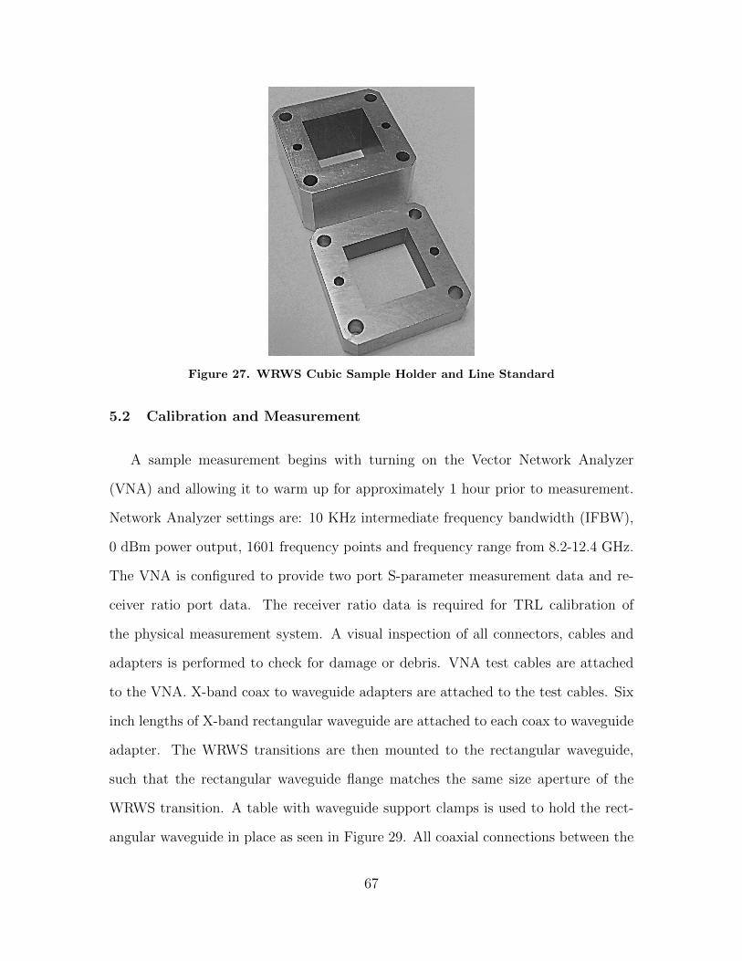
Figure 27. WRWS Cubic Sample Holder and Line Standard
5.2 Calibration and Measurement
A sample measurement begins with turning on the Vector Network Analyzer
(VNA) and allowing it to warm up for approximately 1 hour prior to measurement.
Network Analyzer settings are: 10 KHz intermediate frequency bandwidth (IFBW),
0 dBm power output, 1601 frequency points and frequency range from 8.2-12.4 GHz.
The VNA is configured to provide two port S-parameter measurement data and re-
ceiver ratio port data. The receiver ratio data is required for TRL calibration of
the physical measurement system. A visual inspection of all connectors, cables and
adapters is performed to check for damage or debris. VNA test cables are attached
to the VNA. X-band coax to waveguide adapters are attached to the test cables. Six
inch lengths of X-band rectangular waveguide are attached to each coax to waveguide
adapter. The WRWS transitions are then mounted to the rectangular waveguide,
such that the rectangular waveguide flange matches the same size aperture of the
WRWS transition. A table with waveguide support clamps is used to hold the rect-
angular waveguide in place as seen in Figure 29. All coaxial connections between the
67

Figure 28. WRWS showing waveguide transition on either side of the sample holder,line standard is placed left of sample holder
68
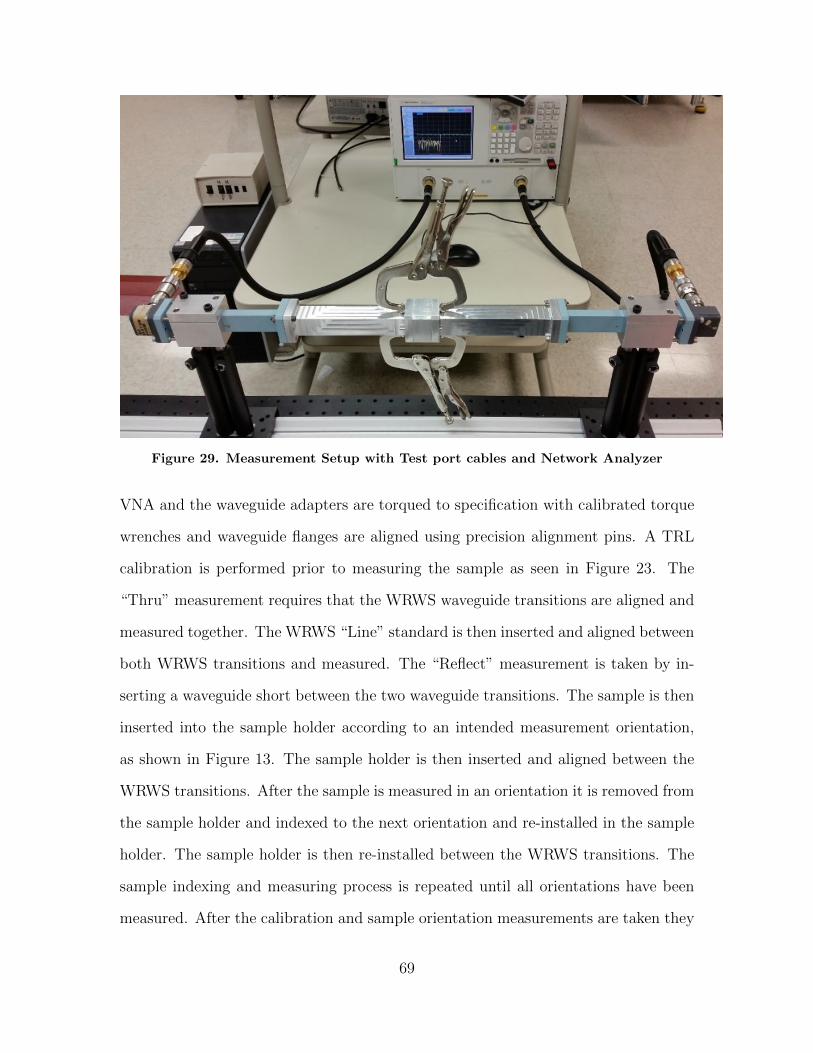
Figure 29. Measurement Setup with Test port cables and Network Analyzer
VNA and the waveguide adapters are torqued to specification with calibrated torque
wrenches and waveguide flanges are aligned using precision alignment pins. A TRL
calibration is performed prior to measuring the sample as seen in Figure 23. The
“Thru” measurement requires that the WRWS waveguide transitions are aligned and
measured together. The WRWS “Line” standard is then inserted and aligned between
both WRWS transitions and measured. The “Reflect” measurement is taken by in-
serting a waveguide short between the two waveguide transitions. The sample is then
inserted into the sample holder according to an intended measurement orientation,
as shown in Figure 13. The sample holder is then inserted and aligned between the
WRWS transitions. After the sample is measured in an orientation it is removed from
the sample holder and indexed to the next orientation and re-installed in the sample
holder. The sample holder is then re-installed between the WRWS transitions. The
sample indexing and measuring process is repeated until all orientations have been
measured. After the calibration and sample orientation measurements are taken they
69
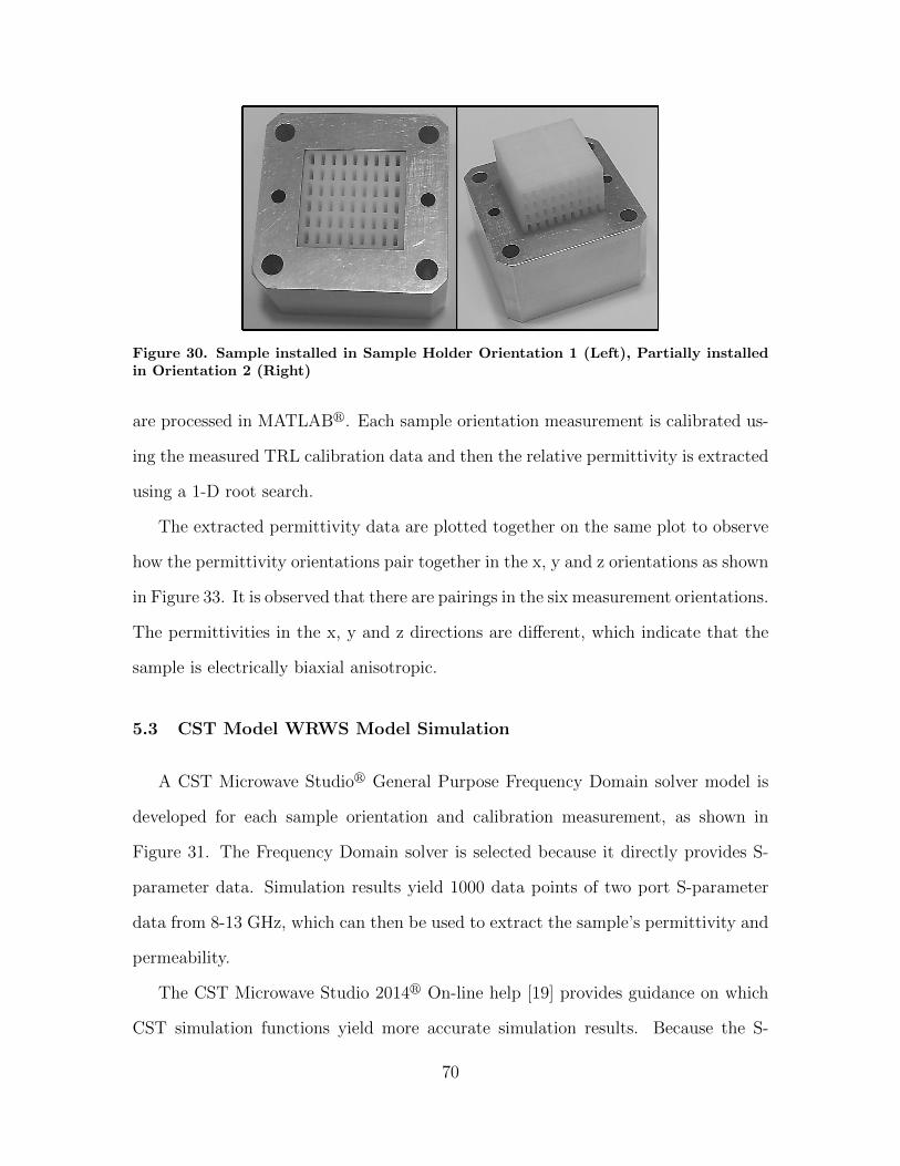
Figure 30. Sample installed in Sample Holder Orientation 1 (Left), Partially installedin Orientation 2 (Right)
are processed in MATLABr. Each sample orientation measurement is calibrated us-
ing the measured TRL calibration data and then the relative permittivity is extracted
using a 1-D root search.
The extracted permittivity data are plotted together on the same plot to observe
how the permittivity orientations pair together in the x, y and z orientations as shown
in Figure 33. It is observed that there are pairings in the six measurement orientations.
The permittivities in the x, y and z directions are different, which indicate that the
sample is electrically biaxial anisotropic.
5.3 CST Model WRWS Model Simulation
A CST Microwave Studior General Purpose Frequency Domain solver model is
developed for each sample orientation and calibration measurement, as shown in
Figure 31. The Frequency Domain solver is selected because it directly provides S-
parameter data. Simulation results yield 1000 data points of two port S-parameter
data from 8-13 GHz, which can then be used to extract the sample’s permittivity and
permeability.
The CST Microwave Studio 2014r On-line help [19] provides guidance on which
CST simulation functions yield more accurate simulation results. Because the S-
70
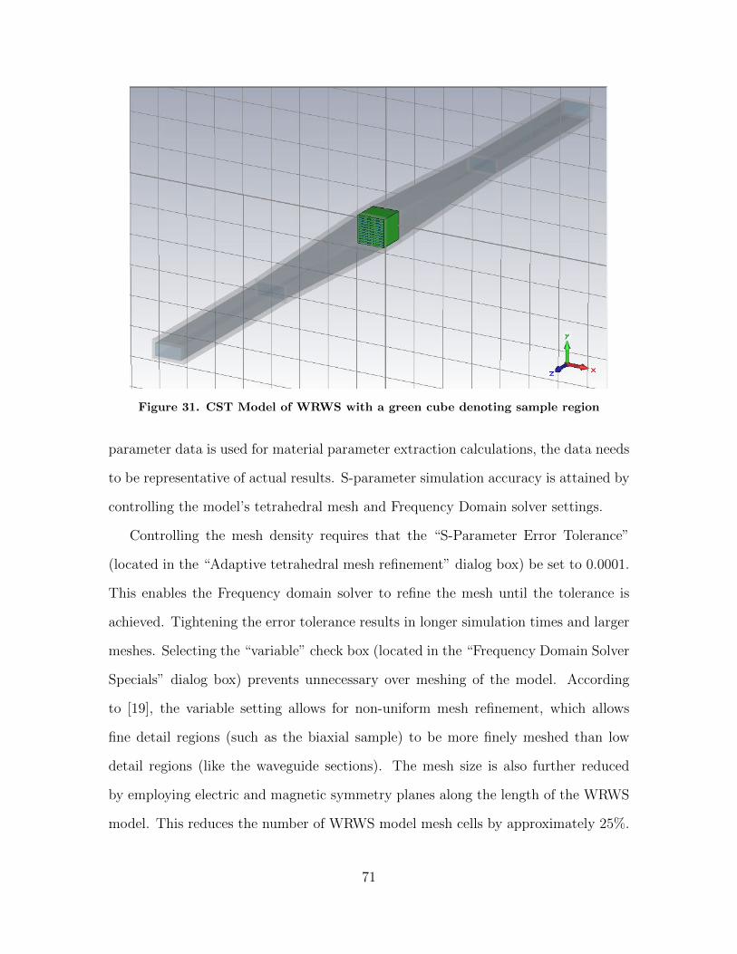
Figure 31. CST Model of WRWS with a green cube denoting sample region
parameter data is used for material parameter extraction calculations, the data needs
to be representative of actual results. S-parameter simulation accuracy is attained by
controlling the model’s tetrahedral mesh and Frequency Domain solver settings.
Controlling the mesh density requires that the “S-Parameter Error Tolerance”
(located in the “Adaptive tetrahedral mesh refinement” dialog box) be set to 0.0001.
This enables the Frequency domain solver to refine the mesh until the tolerance is
achieved. Tightening the error tolerance results in longer simulation times and larger
meshes. Selecting the “variable” check box (located in the “Frequency Domain Solver
Specials” dialog box) prevents unnecessary over meshing of the model. According
to [19], the variable setting allows for non-uniform mesh refinement, which allows
fine detail regions (such as the biaxial sample) to be more finely meshed than low
detail regions (like the waveguide sections). The mesh size is also further reduced
by employing electric and magnetic symmetry planes along the length of the WRWS
model. This reduces the number of WRWS model mesh cells by approximately 25%.
71
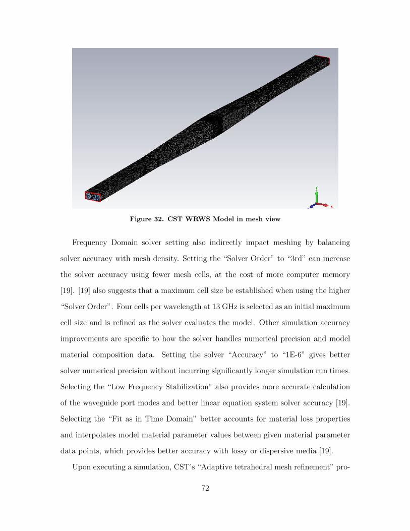
Figure 32. CST WRWS Model in mesh view
Frequency Domain solver setting also indirectly impact meshing by balancing
solver accuracy with mesh density. Setting the “Solver Order” to “3rd” can increase
the solver accuracy using fewer mesh cells, at the cost of more computer memory
[19]. [19] also suggests that a maximum cell size be established when using the higher
“Solver Order”. Four cells per wavelength at 13 GHz is selected as an initial maximum
cell size and is refined as the solver evaluates the model. Other simulation accuracy
improvements are specific to how the solver handles numerical precision and model
material composition data. Setting the solver “Accuracy” to “1E-6” gives better
solver numerical precision without incurring significantly longer simulation run times.
Selecting the “Low Frequency Stabilization” also provides more accurate calculation
of the waveguide port modes and better linear equation system solver accuracy [19].
Selecting the “Fit as in Time Domain” better accounts for material loss properties
and interpolates model material parameter values between given material parameter
data points, which provides better accuracy with lossy or dispersive media [19].
Upon executing a simulation, CST’s “Adaptive tetrahedral mesh refinement” pro-
72

Table 3. CST Simulation Performance Figures
Simulation Run Time(hr:min:sec)
TetrahedralMesh Cells
Degrees offreedom
Freq. Pts.needed for
convergence
AdaptiveMesh
Refinementiterations
Thru 0:10:30 27,624 474,490 53 10Reflect 0:00:20 1,852 10,506 42 1Line 0:10:20 24,765 423,025 59 9
Sample O-1 1:12:50 102,373 1,543,531 60 23Sample O-2 1:27:37 99,751 1,542,942 55 19Sample O-3 0:49:07 60,602 938,241 56 12Sample O-4 0:49:39 65,255 1,007,366 51 13Sample O-5 1:13:06 75,494 1,126,896 53 16Sample O-6 1:09:00 82,414 1,240,252 54 16
cess refines the mesh until successive 13 GHz S-parameter trials converge to the spec-
ified “S-Parameter Error Tolerance” of 0.0001. The solver then evaluates the model
at different frequencies within the 8-13 GHz band, until the entire band of two port
S-parameter measurements converges within the error tolerance. Figure 32 shows a
typical WRWS system mesh and Table 3 shows simulation performance data. The
simulated S-parameter data is transferred to MATLABr and each simulated mea-
surement orientation is calibrated from the simulated TRL calibration data. The
permittivity of each calibrated orientation is extracted and prediction results are
compared to measured data. Excellent agreement is observed between measured and
simulated results, as seen in Figures 33 and 34.
73
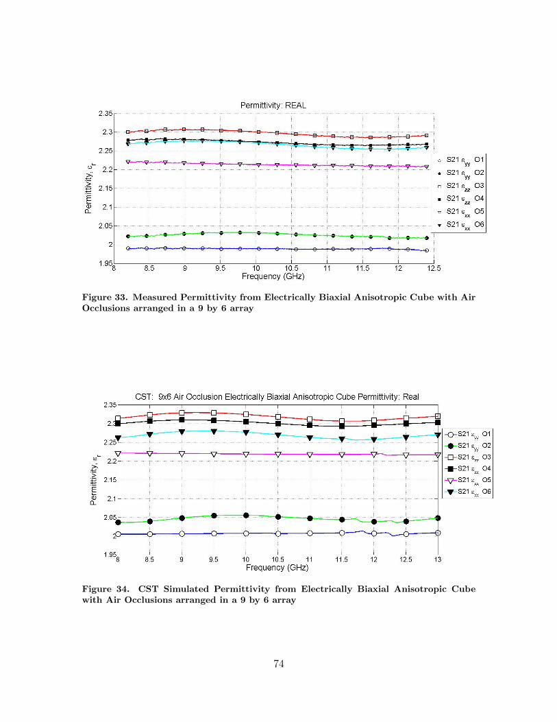
Figure 33. Measured Permittivity from Electrically Biaxial Anisotropic Cube with AirOcclusions arranged in a 9 by 6 array
Figure 34. CST Simulated Permittivity from Electrically Biaxial Anisotropic Cubewith Air Occlusions arranged in a 9 by 6 array
74
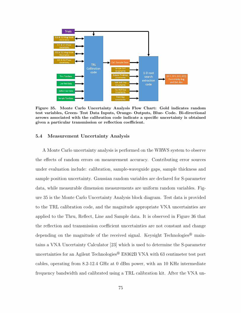
Figure 35. Monte Carlo Uncertainty Analysis Flow Chart: Gold indicates randomtest variables, Green- Test Data Inputs, Orange- Outputs, Blue- Code. Bi-directionalarrows associated with the calibration code indicate a specific uncertainty is obtainedgiven a particular transmission or reflection coefficient.
5.4 Measurement Uncertainty Analysis
A Monte Carlo uncertainty analysis is performed on the WRWS system to observe
the effects of random errors on measurement accuracy. Contributing error sources
under evaluation include: calibration, sample-waveguide gaps, sample thickness and
sample position uncertainty. Gaussian random variables are declared for S-parameter
data, while measurable dimension measurements are uniform random variables. Fig-
ure 35 is the Monte Carlo Uncertainty Analysis block diagram. Test data is provided
to the TRL calibration code, and the magnitude appropriate VNA uncertainties are
applied to the Thru, Reflect, Line and Sample data. It is observed in Figure 36 that
the reflection and transmission coefficient uncertainties are not constant and change
depending on the magnitude of the received signal. Keysight Technologiesr main-
tains a VNA Uncertainty Calculator [23] which is used to determine the S-parameter
uncertainties for an Agilent Technologiesr E8362B VNA with 63 centimeter test port
cables, operating from 8.2-12.4 GHz at 0 dBm power, with an 10 KHz intermediate
frequency bandwidth and calibrated using a TRL calibration kit. After the VNA un-
75

Figure 36. VNA Uncertainty vs Reflection (Top) and Transmission (Bottom) generatedfor the Agilent Technologiesr E8362B VNA from the Keysight Technologiesr VNAuncertainty calculator.
certainties are applied and the TRL calibration performed, the permittivity is then
extracted from the calibrated sample data using a 1-D root search extraction Monte
Carlo analysis, which applies sample thickness, position, and gap uncertainties. Gap
uncertainties are accounted as gap corrections to the 1-D root search results. An
equivalent capacitance lumped element model corrects the permittivity caused by
potential gaps present on three sides of the sample. Gaps are assumed on top, the
front and 1 side of the sample, as shown in Figure 37. Uniform random variables are:
gyRV , a gap in the y direction; gxRV , a gap in the x direction; lRV is the gap in sample
thickness. l is the sample edge length. The sample’s measured permittivity can be
76
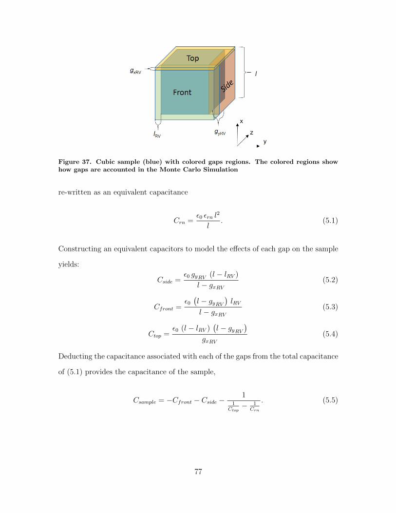
Figure 37. Cubic sample (blue) with colored gaps regions. The colored regions showhow gaps are accounted in the Monte Carlo Simulation
re-written as an equivalent capacitance
Crn =ε0 εrn l
2
l. (5.1)
Constructing an equivalent capacitors to model the effects of each gap on the sample
yields:
Cside =ε0 gyRV (l − lRV )
l − gxRV(5.2)
Cfront =ε0(l − gyRV
)lRV
l − gxRV(5.3)
Ctop =ε0 (l − lRV )
(l − gyRV
)gxRV
(5.4)
Deducting the capacitance associated with each of the gaps from the total capacitance
of (5.1) provides the capacitance of the sample,
Csample = −Cfront − Cside −1
1Ctop− 1
Crn
. (5.5)
77
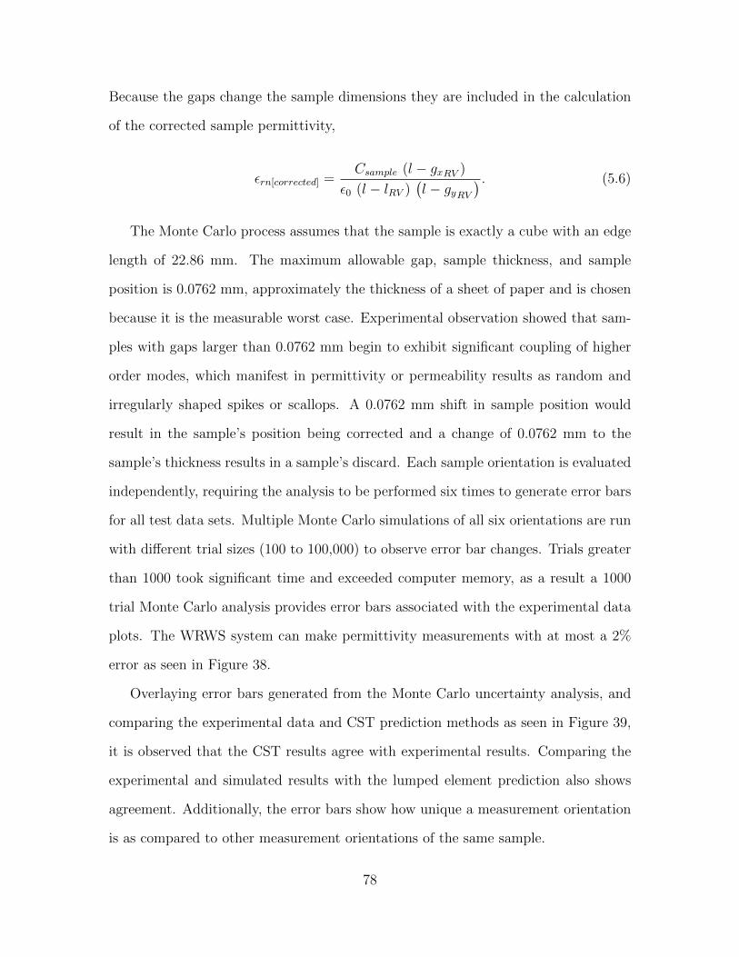
Because the gaps change the sample dimensions they are included in the calculation
of the corrected sample permittivity,
εrn[corrected] =Csample (l − gxRV )
ε0 (l − lRV )(l − gyRV
) . (5.6)
The Monte Carlo process assumes that the sample is exactly a cube with an edge
length of 22.86 mm. The maximum allowable gap, sample thickness, and sample
position is 0.0762 mm, approximately the thickness of a sheet of paper and is chosen
because it is the measurable worst case. Experimental observation showed that sam-
ples with gaps larger than 0.0762 mm begin to exhibit significant coupling of higher
order modes, which manifest in permittivity or permeability results as random and
irregularly shaped spikes or scallops. A 0.0762 mm shift in sample position would
result in the sample’s position being corrected and a change of 0.0762 mm to the
sample’s thickness results in a sample’s discard. Each sample orientation is evaluated
independently, requiring the analysis to be performed six times to generate error bars
for all test data sets. Multiple Monte Carlo simulations of all six orientations are run
with different trial sizes (100 to 100,000) to observe error bar changes. Trials greater
than 1000 took significant time and exceeded computer memory, as a result a 1000
trial Monte Carlo analysis provides error bars associated with the experimental data
plots. The WRWS system can make permittivity measurements with at most a 2%
error as seen in Figure 38.
Overlaying error bars generated from the Monte Carlo uncertainty analysis, and
comparing the experimental data and CST prediction methods as seen in Figure 39,
it is observed that the CST results agree with experimental results. Comparing the
experimental and simulated results with the lumped element prediction also shows
agreement. Additionally, the error bars show how unique a measurement orientation
is as compared to other measurement orientations of the same sample.
78
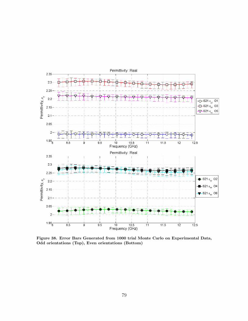
Figure 38. Error Bars Generated from 1000 trial Monte Carlo on Experimental Data,Odd orientations (Top), Even orientations (Bottom)
79

Figure 39. Comparison of Simulation Data with Experimental Uncertainty Data Oddorientations (Top), Even orientations (Bottom)
80

Figure 40. Comparison of Vertical arrangement Lumped Element Data and SimulationData with Experimental Uncertainty Data Odd orientations (Top), Even orientations(Bottom)
81
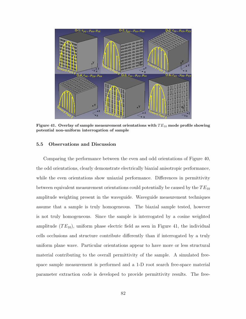
Figure 41. Overlay of sample measurement orientations with TE10 mode profile showingpotential non-uniform interrogation of sample
5.5 Observations and Discussion
Comparing the performance between the even and odd orientations of Figure 40,
the odd orientations, clearly demonstrate electrically biaxial anisotropic performance,
while the even orientations show uniaxial performance. Differences in permittivity
between equivalent measurement orientations could potentially be caused by the TE10
amplitude weighting present in the waveguide. Waveguide measurement techniques
assume that a sample is truly homogeneous. The biaxial sample tested, however
is not truly homogeneous. Since the sample is interrogated by a cosine weighted
amplitude (TE10), uniform phase electric field as seen in Figure 41, the individual
cells occlusions and structure contribute differently than if interrogated by a truly
uniform plane wave. Particular orientations appear to have more or less structural
material contributing to the overall permittivity of the sample. A simulated free-
space sample measurement is performed and a 1-D root search free-space material
parameter extraction code is developed to provide permittivity results. The free-
82
Figure 42. TEM Free Space CST Measure of an infinite array of cubes arranged in aslab
space CST material measurement modeling concept is based on [24]’s approach. TRL
calibrated and extracted results from the CST model are shown in Figure 42 which
assumes uniform plane wave interrogation of an infinite slab made of the sample
cubes, as shown in Figure 43. Changing the interrogating field amplitude from a
cosine weighting (WRWS) to a uniform weighting (free-space) causes the x, y, z
paired permittivity orientation to be almost equivalent. Another contributing factor
to equivalent orientations yielding slightly different values could be caused by the
occlusion array not being printed perfectly symmetric and centered within the sample.
The occlusion array being biased would cause more or less material to appear present
depending on the sample’s orientation within the waveguide.
5.6 Electrically Biaxial Anisotropic Samples using different materials
Despite the weighting effect, biaxial anisotropic performance is more easily ob-
served by increasing the permittivity contrast between structure and inclusion ma-
terials. A sample simulated in CST Microwave Studior with the same UV cured
polymer structure and alumina inclusions, instead of air occlusion enhances the sepa-
83
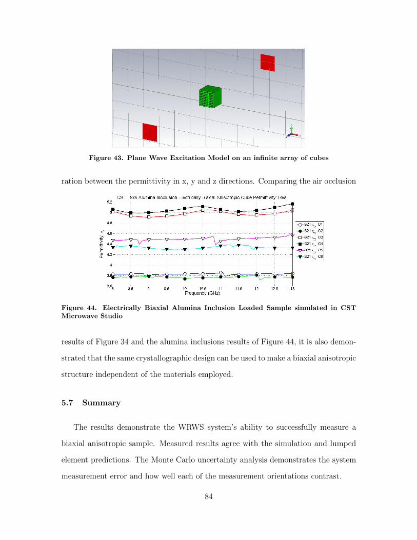
Figure 43. Plane Wave Excitation Model on an infinite array of cubes
ration between the permittivity in x, y and z directions. Comparing the air occlusion
Figure 44. Electrically Biaxial Alumina Inclusion Loaded Sample simulated in CSTMicrowave Studio
results of Figure 34 and the alumina inclusions results of Figure 44, it is also demon-
strated that the same crystallographic design can be used to make a biaxial anisotropic
structure independent of the materials employed.
5.7 Summary
The results demonstrate the WRWS system’s ability to successfully measure a
biaxial anisotropic sample. Measured results agree with the simulation and lumped
element predictions. The Monte Carlo uncertainty analysis demonstrates the system
measurement error and how well each of the measurement orientations contrast.
84
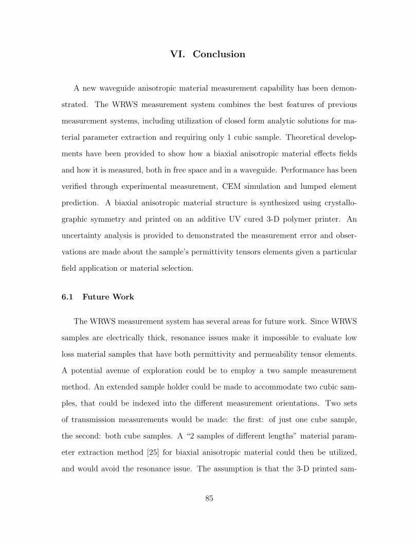
VI. Conclusion
A new waveguide anisotropic material measurement capability has been demon-
strated. The WRWS measurement system combines the best features of previous
measurement systems, including utilization of closed form analytic solutions for ma-
terial parameter extraction and requiring only 1 cubic sample. Theoretical develop-
ments have been provided to show how a biaxial anisotropic material effects fields
and how it is measured, both in free space and in a waveguide. Performance has been
verified through experimental measurement, CEM simulation and lumped element
prediction. A biaxial anisotropic material structure is synthesized using crystallo-
graphic symmetry and printed on an additive UV cured 3-D polymer printer. An
uncertainty analysis is provided to demonstrated the measurement error and obser-
vations are made about the sample’s permittivity tensors elements given a particular
field application or material selection.
6.1 Future Work
The WRWS measurement system has several areas for future work. Since WRWS
samples are electrically thick, resonance issues make it impossible to evaluate low
loss material samples that have both permittivity and permeability tensor elements.
A potential avenue of exploration could be to employ a two sample measurement
method. An extended sample holder could be made to accommodate two cubic sam-
ples, that could be indexed into the different measurement orientations. Two sets
of transmission measurements would be made: the first: of just one cube sample,
the second: both cube samples. A “2 samples of different lengths” material param-
eter extraction method [25] for biaxial anisotropic material could then be utilized,
and would avoid the resonance issue. The assumption is that the 3-D printed sam-
85

ple production is sufficiently consistent. This technique would be equally or more
advantageous as compared to previous techniques because the sample can still be
indexed and only requires 2 samples, as opposed to the 3 unique samples required for
rectangular waveguide techniques.
Another area of research, is to explore magnetic samples in a crystallographic de-
sign. A magnetically biaxial sample could be designed using small ferrous inclusions,
such as Nickel. Provided the structural material possesses the same dielectric contrast
as the magnetic material, a 1-D root search could be made for a sample’s permeability,
assuming the permittivity is known. If the 2 sample technique is successfully utilized
then materials that exhibit both electric and magnetic biaxial performance could be
studied within the same sample.
A final research area, would be to utilize free-space measurement techniques, such
as a focus beam system and measure the biaxial anisotropic performance of an array
of cubics samples arranged in a sheet. The cubic samples could be indexed through
their measurement orientations within the sheet structure, which would allow for
all six measurement orientations to be measured at normal incidence. Additionally,
the free-space mathematical development of Chapter 2 could be utilized to support
sample measurements at oblique incidence. The difficulty in the oblique evaluation is
the additional antennas needed to measure both polarizations for both transmitted
and reflected field components.
86
Bibliography
1. A. Nicolson and G. F. Ross, “Measurement of the intrinsic properties of mate-rials by time-domain techniques,” IEEE Transactions on Instrumentation andMeasurement, vol. 19, no. 4, pp. 377–382, 1970.
2. W. B. Weir, “Automatic measurement of complex dielectric constant and per-meability at microwave frequencies,” Proceedings of the IEEE, vol. 62, no. 1, pp.33–36, 1974.
3. T. Blakney and W. Weir, “Comments on ”automatic measurement of complexdielectric constant and permeability at microwave frequencies”,” Proceedings ofthe IEEE, vol. 63, no. 1, pp. 203–205, Jan 1975.
4. J. Baker-Jarvis, E. Vanzura, and W. Kissick, “Improved technique for determin-ing complex permittivity with the transmission/reflection method,” IEEE Trans-actions on Microwave Theory and Techniques, vol. 38, no. 8, pp. 1096–1103, 1990.
5. N. Damaskos, R. Mack, A. Maffett, W. Parmon, and P. L. E. Uslenghi, “Theinverse problem for biaxial materials,” IEEE Transactions on Microwave Theoryand Techniques, vol. 32, no. 4, pp. 400–405, 1984.
6. B. Crowgey, O. Tuncer, J. Tang, E. Rothwell, B. Shanker, L. Kempel, andM. Havrilla, “Characterization of biaxial anisotropic material using a reducedaperture waveguide,” IEEE Transactions on Instrumentation and Measurement,vol. 62, no. 10, pp. 2739–2750, Oct 2013.
7. J. Tang, B. Crowgey, O. Tuncer, L. Kempel, E. Rothwell, and B. Shanker, “Char-acterization of biaxial materials using a partially filled rectangular waveguide,”in 34th Annual Symposium of the Antenna Measurement Techniques AssociationConference Proceeding, October 2012, pp. 437–442.
8. A. Knisely, M. Havrilla, P. Collins, M. Hyde, J. Allen, A. Bogle, and E. Roth-well, “Biaxial anisotropic material characterization using rectangular to squarewaveguide,” in 36th Annual Symposium of the Antenna Measurement TechniquesAssociation Conference Proceedings, October 2014, pp. 437–442.
9. R. Collin, “A simple artificial anisotropic dielectric medium,” IRE Transactionson Microwave Theory and Techniques, vol. 6, no. 2, pp. 206–209, 1958.
10. V. Dmitriev, “Tables of the second rank constitutive tensors for linear homoge-neous media described by the point magnetic groups of symmetry,” Progress InElectromagnetics Research, vol. 28, pp. 43–95, 2000.
11. C. Balanis, Advanced Engineering Electromagnetics, ser. CourseSmart Series.Wiley, 2012.
87
12. A. Knisely and M. J. Havrilla, “Material characterization de-embedding for rect-angular to square waveguide,” in The 9th European Conference on Antennas andPropagation (EuCAP 2015) (EuCAP 2015), Lisbon, Portugal, Apr. 2015.
13. D. Pozar, Microwave Engineering. Wiley, 2004.
14. M. Havrilla, M. Hyde and A. Bogle, “Improved bandwidth in rectangular waveg-uide material characterization measurements,” in 36th Annual Symposium of theAntenna Measurement Techniques Association Conference Proceedings, October2014, pp. 427–431.
15. T. Hahn, International Tables for Crystallography-Volume A: “Space-Group Sym-metry”. Springer, 2005.
16. A. Authier, International Tables for Crystallography-Volume D: “Physical Prop-erties of Crystals”. Kluwer Academic Publishers, 2003.
17. S. Patil, M. Koledintseva, R. Schwartz, and W. Huebner, “Prediction of effec-tive permittivity of diphasic dielectrics using an equivalent capacitance model,”Journal of Applied Physics, vol. 104, no. 7, pp. 074 108–074 108–11, Oct 2008.
18. W. Hayt and J. Buck, Engineering Electromagnetics, ser. Electrical engineeringseries. McGraw-Hill Education, 2001.
19. “Cst microwave studio suite online help,” CST Microwave Studio 2014. [Online].Available: https://www.cst.com/
20. G. F. Engen and C. A. Hoer, “Thru-reflect-line: An improved technique forcalibrating the dual six-port automatic network analyzer,” IEEE Transactionson Microwave Theory and Techniques, vol. 27, no. 12, pp. 987–993, Dec 1979.
21. D. Rytting, “An analysis of vector measurement accuracy enhancement tech-niques,” RF and Microwave Symposium and Exhibition, Hewlett Packard, March1982.
22. ——, “Appendix to an analysis of vector measurement accuracy enhancementtechniques,” RF and Microwave Symposium and Exhibition, Hewlett Packard,March 1982.
23. “Downloadable vector network analyzer uncertainty calculator,” KeysightTechnologies Software. [Online]. Available: http://www.keysight.com/main/home.jspx?cc=US&lc=eng
24. D. Schurig, “Assignments,” ECE 5350/6350 Fall 2013 Metamaterials andAdvanced Antenna Theory. [Online]. Available: http://www.ece.utah.edu/∼dschurig/5/ECE 5350 and 6350 Fall 2013/Assignments.html
88

25. J. Baker-Jarvis, M. Janezic, J. Grosvenor, and R. Geyer, “Transmission/reflectionand short-circuit line methods for measuring permittivity and permeability,” Natl.Inst. Stand. Technol., Tech. Note 1355-R, p. 20, 1993.
89

REPORT DOCUMENTATION PAGE Form ApprovedOMB No. 0704–0188
The public reporting burden for this collection of information is estimated to average 1 hour per response, including the time for reviewing instructions, searching existing data sources, gathering andmaintaining the data needed, and completing and reviewing the collection of information. Send comments regarding this burden estimate or any other aspect of this collection of information, includingsuggestions for reducing this burden to Department of Defense, Washington Headquarters Services, Directorate for Information Operations and Reports (0704–0188), 1215 Jefferson Davis Highway,Suite 1204, Arlington, VA 22202–4302. Respondents should be aware that notwithstanding any other provision of law, no person shall be subject to any penalty for failing to comply with a collectionof information if it does not display a currently valid OMB control number. PLEASE DO NOT RETURN YOUR FORM TO THE ABOVE ADDRESS.
1. REPORT DATE (DD–MM–YYYY) 2. REPORT TYPE 3. DATES COVERED (From — To)
4. TITLE AND SUBTITLE 5a. CONTRACT NUMBER
5b. GRANT NUMBER
5c. PROGRAM ELEMENT NUMBER
5d. PROJECT NUMBER
5e. TASK NUMBER
5f. WORK UNIT NUMBER
6. AUTHOR(S)
7. PERFORMING ORGANIZATION NAME(S) AND ADDRESS(ES) 8. PERFORMING ORGANIZATION REPORTNUMBER
9. SPONSORING / MONITORING AGENCY NAME(S) AND ADDRESS(ES) 10. SPONSOR/MONITOR’S ACRONYM(S)
11. SPONSOR/MONITOR’S REPORTNUMBER(S)
12. DISTRIBUTION / AVAILABILITY STATEMENT
13. SUPPLEMENTARY NOTES
14. ABSTRACT
15. SUBJECT TERMS
16. SECURITY CLASSIFICATION OF:
a. REPORT b. ABSTRACT c. THIS PAGE
17. LIMITATION OFABSTRACT
18. NUMBEROFPAGES
19a. NAME OF RESPONSIBLE PERSON
19b. TELEPHONE NUMBER (include area code)
Standard Form 298 (Rev. 8–98)Prescribed by ANSI Std. Z39.18
26–03–2015 Master’s Thesis Sept 2013 — Mar 2015
Biaxial AnisotropicMaterial Development and Characterization using
Rectangular to Square Waveguide
Knisely, Alexander G., Mr., Civ.
Air Force Institute of TechnologyGraduate School of Engineering and Management (AFIT/EN)2950 Hobson WayWPAFB OH 45433-7765
AFIT-ENG-MS-15-M-055
Air Force Research Laboratory, Sensors DirectorateAttn: Garrett J. Stenholm2591 K Street, Bldg 254WPAFB OH 45433-7602DSN 785-9179, COMM 937-255-9179Email: [email protected]
AFRL/RYS
DISTRIBUTION STATEMENT A:APPROVED FOR PUBLIC RELEASE; DISTRIBUTION UNLIMITED.
This material is declared a work of the U.S. Government and is not subject to copytight protection in the United States.
The advent of 3-D printing provides a new way to develop complex electromagnetic media. Complex media poses measurement challengesand require new techniques to characterize sample constitutive parameters. A biaxial anisotropic sample is designed using crystallographicsymmetry and tensor elements are predicted using equivalent capacitive and inductive lumped elements. Samples are measured using theWaveguide Rectangular to Waveguide Square (WRWS) cubic sample measurement system. The WRWS system supports the analysis of acubic biaxial anisotropic sample by measuring the sample in different measurement orientations. The orientation S-parameter data is usedto extract tensor element permittivites and permeabilities using an analytic, closed-form technique. Research performed in this documentdemonstrates a sample synthesis methodology, a measurement representative computational electromagnetic (CEM) prediction of WRWSsample measurements and tests results of an electrically biaxial sample. An uncertainty analysis is also conducted on the experimental datato evaluate potential error sources. The lumped element and CEM predictions agree with the test results. Supplemental discussion alsoprovides a comparison between test data and a free-space simulated results as well as simulated example of an electrically biaxial sampleloaded with alumina. These two examples demonstrate the utility of a crystallographic sample design.
RF Material Characterization, Anisotropic, Biaxial, Electromagnetics, Tapered Waveguide, Metamaterials
U U U UU 104
Dr. Michael J. Havrilla, AFIT/ENG
(937) 255-3636, x4582 [email protected]