Embed Size (px)
Citation preview

Power Management & Mult imarket
Datasheet Revision 1.9.2, 2014-04-02Final
BGF1487 line ESD and EMI interface protection device
BGF148

Edition 2014-04-02Published byInfineon Technologies AG81726 Munich, Germany© 2014 Infineon Technologies AGAll Rights Reserved.
InformationFor further information on technology, delivery terms and conditions and prices, please contact the nearestInfineon Technologies Office (www.infineon.com)
WarningsDue to technical requirements, components may contain dangerous substances. For information on the types inquestion, please contact the nearest Infineon Technologies Office.Infineon Technologies components may be used in life-support devices or systems only with the express writtenapproval of Infineon Technologies, if a failure of such components can reasonably be expected to cause the failureof that life-support device or system or to affect the safety or effectiveness of that device or system. Life supportdevices or systems are intended to be implanted in the human body or to support and/or maintain and sustainand/or protect human life. If they fail, it is reasonable to assume that the health of the user or other persons maybe endangered.

BGF148
Final Datasheet 3 Revision 1.9.2, 2014-04-02
Trademarks of Infineon Technologies AGAURIX™, C166™, CanPAK™, CIPOS™, CIPURSE™, EconoPACK™, CoolMOS™, CoolSET™,CORECONTROL™, CROSSAVE™, DAVE™, DI-POL™, EasyPIM™, EconoBRIDGE™, EconoDUAL™,EconoPIM™, EconoPACK™, EiceDRIVER™, eupec™, FCOS™, HITFET™, HybridPACK™, I²RF™,ISOFACE™, IsoPACK™, MIPAQ™, ModSTACK™, my-d™, NovalithIC™, OptiMOS™, ORIGA™,POWERCODE™; PRIMARION™, PrimePACK™, PrimeSTACK™, PRO-SIL™, PROFET™, RASIC™,ReverSave™, SatRIC™, SIEGET™, SINDRION™, SIPMOS™, SmartLEWIS™, SOLID FLASH™, TEMPFET™,thinQ!™, TRENCHSTOP™, TriCore™.
Other TrademarksAdvance Design System™ (ADS) of Agilent Technologies, AMBA™, ARM™, MULTI-ICE™, KEIL™,PRIMECELL™, REALVIEW™, THUMB™, µVision™ of ARM Limited, UK. AUTOSAR™ is licensed by AUTOSARdevelopment partnership. Bluetooth™ of Bluetooth SIG Inc. CAT-iq™ of DECT Forum. COLOSSUS™,FirstGPS™ of Trimble Navigation Ltd. EMV™ of EMVCo, LLC (Visa Holdings Inc.). EPCOS™ of Epcos AG.FLEXGO™ of Microsoft Corporation. FlexRay™ is licensed by FlexRay Consortium. HYPERTERMINAL™ ofHilgraeve Incorporated. IEC™ of Commission Electrotechnique Internationale. IrDA™ of Infrared DataAssociation Corporation. ISO™ of INTERNATIONAL ORGANIZATION FOR STANDARDIZATION. MATLAB™ ofMathWorks, Inc. MAXIM™ of Maxim Integrated Products, Inc. MICROTEC™, NUCLEUS™ of Mentor GraphicsCorporation. MIPI™ of MIPI Alliance, Inc. MIPS™ of MIPS Technologies, Inc., USA. muRata™ of MURATAMANUFACTURING CO., MICROWAVE OFFICE™ (MWO) of Applied Wave Research Inc., OmniVision™ ofOmniVision Technologies, Inc. Openwave™ Openwave Systems Inc. RED HAT™ Red Hat, Inc. RFMD™ RFMicro Devices, Inc. SIRIUS™ of Sirius Satellite Radio Inc. SOLARIS™ of Sun Microsystems, Inc. SPANSION™of Spansion LLC Ltd. Symbian™ of Symbian Software Limited. TAIYO YUDEN™ of Taiyo Yuden Co.TEAKLITE™ of CEVA, Inc. TEKTRONIX™ of Tektronix Inc. TOKO™ of TOKO KABUSHIKI KAISHA TA. UNIX™of X/Open Company Limited. VERILOG™, PALLADIUM™ of Cadence Design Systems, Inc. VLYNQ™ of TexasInstruments Incorporated. VXWORKS™, WIND RIVER™ of WIND RIVER SYSTEMS, INC. ZETEX™ of DiodesZetex Limited.Last Trademarks Update 2011-11-11
Revision History Rev. 1.9.1, 2014-01-17Page or Item Subjects (major changes since previous revision)Revision 1.9.2, 2014-04-025 Table 2-1) updated

BGF148
7 line ESD and EMI interface protection device
Final Datasheet 4 Revision 1.9.2, 2014-04-02
1 7 line ESD and EMI interface protection device
1.1 Features
1.2 Application
• High-Speed Mini-/Micro- SD Card ESD protection and EMI filter• SD3.0 card Interface (Mini, Micro), down compatible to SD2.0 and lower
– feature phones, smart phones, tablets, digital still cameras, digital video cameras, computers and other devices using SD card interfaces
• 7 line bidirectional ESD protection• ESD protection according to IEC61000-4-2 for ±15 kV contact discharge on all external IOs• ESD protection according to IEC61000-4-2 for ±8 kV contact discharge on all internal IOs• 6 line pi-type EMI filter for superior EMI filtering and very low cross-talk due to low parasitics• Suitable for high speed applications due to low line capacitance of typical 1.2 pF• Very low voltage dependency of line capacitance• Very low leakage currents• Application requires very small PCB area using an optimized I/O arrangement• Small sized Plastic Package with 400 μm pitch• Pb-free (RoHS compliant) and halogen free package• Complies with following standards: SD Card Specification V4.1 including UHS104 mode

BGF148
Electrical Characteristics
Final Datasheet 5 Revision 1.9.2, 2014-04-02
1.3 Product Description
Figure 1-1 Schematic
2 Electrical Characteristics
2.1 Maximum Ratings
Attention: Stresses above the max. values listed here may cause permanent damage to the device. Exposure to absolute maximum rating conditions for extended periods may affect device reliability. Maximum ratings are absolute ratings; exceeding only one of these values may cause irreversible damage to the integrated circuit.
Type Package Marking ChipBGF148 TSNP-14-2 48 N0756
Table 2-1 Maximum Ratings at TA = 25 °C, unless otherwise specified
Parameter Symbol Values Unit Note / Test ConditionMin. Typ. Max.
Voltage at all pins to GND VF 0 - 5.5 VOperating temperature range TOP -40 - +85 °CStorage temperature range TSTG -65 - +150 °C ESD contact discharge1) External IOsInternal IOs1) VESD according to IEC61000-4-2
VESD-15-8
-158
kV
BGF148_schematic_pin_diagram.vsdTop view
SDdat 3/CD
GND
SDdat 2
SDdat 1
SDdat 0
SDcmd
SDclk
Dat3/CD
dat 2
dat1
dat 0
cmd
clk
VCC IO
R1: 20 Ω
R2: 20 Ω
R3: 20 Ω
R4: 20 Ω
R5: 20 Ω
R6: 20 Ω
HOST
CARD
Int. PINs8kV ESD+
−
Ext. PIN15kV ESD+
−
SDdat3/CD
SDCMD
GND
SDclk
SDdat0
SDdat1 dat1
SDdat2
dat2
dat3/CD
CMD
Vcc
clk
dat0
14
1
2
3
4
5
67
8
9
10
11
12
13
GND

BGF148
Electrical Characteristics
Final Datasheet 6 Revision 1.9.2, 2014-04-02
2.2 Electrical Characteristics
Table 2-2 DC Characteristics at TA = 25 °C, unless otherwise specified
Parameter Symbol Values Unit Note / Test ConditionMin. Typ. Max.
Resistor R1...R6 R1...R6 18 20 22 ΩReverse current of ESD diodes IR - 5 100 nA VR = 5.5 VBreakdown voltage of ESD diodes VBR - 6.5 - V IBR = 1 mA
Table 2-3 RF Characteristics at TA = 25 °C, unless otherwise specified
Parameter Symbol Values Unit Note / Test ConditionMin. Typ. Max.
Line capacitance(Capacitance of each line to GND)
CL 1.2 pF VR = 0 V, f = 1 MHz
Table 2-4 ESD Characteristics at TA = 25 °C, unless otherwise specified
Parameter Symbol Values Unit Note / Test ConditionMin. Typ. Max.
Clamping voltage1)2)
1) Pulse at external pins, measurements at related internal pins2) ANSI / ESDSTM5.5.1-Electrostatistic Discharge Sensitivity Testing using Transmission Line Pulse (TLP) Model. TLP
conditions: Z0 = 50 Ω, tp = 100 ns, tr = 0.6 ns, ITLP and VTLP average window: t1 = 30 ns to t2 = 60 ns, extraction of dynamic resistance using squares fit to TLP characteristics between ITLP1 = 2 A and ITLP2 = 15 A. Please refer to Application Note AN210[1]
VCL--
8.59
--
ITLP = 1 AITLP = 16 A
Dynamic resistance1)2) RDYN - 0.03 - Ω

BGF148
Typical Characteristics
Final Datasheet 7 Revision 1.9.2, 2014-04-02
3 Typical CharacteristicsCurves specified at TA = 25 °C, unless otherwise specified
Figure 3-1 Reverse current: IR = f(VR)
Figure 3-2 Line capacitance of line A1 - A4: CL = f(VR), f = 1 MHz
10-12
10-11
10-10
10-9
10-8
10-7
10-6
10-5
10-4
10-3
0 1 2 3 4 5 6 7 8 9
I R [
A]
VR [V]
0
0.2
0.4
0.6
0.8
1
1.2
1.4
1.6
0 0.5 1 1.5 2 2.5 3 3.5 4 4.5 5
CL [
pF
]
VR [V]

BGF148
Typical Characteristics
Final Datasheet 8 Revision 1.9.2, 2014-04-02
Figure 3-3 Measurement setup for clamping voltage
Figure 3-4 Clamping voltage (TLP): ITLP = f(VTLP) according ANSI/ESDSTM5.5.1-Electrostatistic Discharge Sensitivity Testing using Transmission Line Pulse (TLP) Model. TLP conditions: Z0 = 50 Ω, tp = 100 ns, tr = 0.6 ns, ITLP and VTLP average window: t1 = 30 ns to t2 = 60 ns, extraction of dynamic resistance using squares fit to TLP characteristics between ITLP1 = 2 A and ITLP2 = 15 A. Please refer to Application Note AN210[1]
BGF148_VCL.vsd
R_ESD/EMIclk_“SD“
BGF148 clamping voltage measurement
clk_“host“
clamping voltage@ internal pin
ESD current intoexternal pin
0
2
4
6
8
10
12
14
16
18
20
22
24
0 2 4 6 8 10 12 14
I TL
P [
A]
VTLP [V]
BGF148RDYN
RDYN = 0.03 Ω
BGF148
Application Hints
Final Datasheet 9 Revision 1.9.2, 2014-04-02
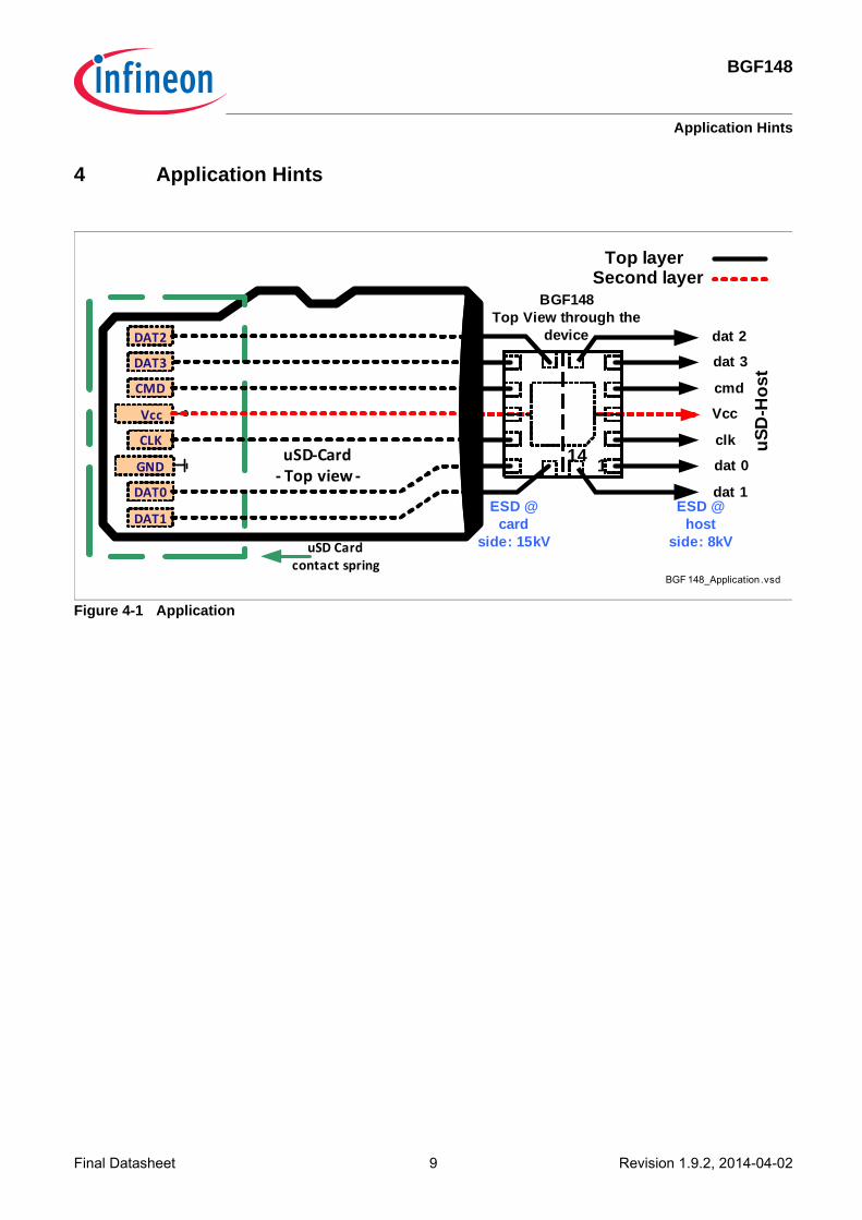
4 Application Hints
Figure 4-1 Application
BGF 148_Application.vsd
uSD Cardcontact spring
Top layerSecond layer
uSD‐Card‐ Top view ‐GND
DAT0
DAT1
CLK
Vcc
CMD
DAT3
DAT2 dat 2
dat 3
cmd
clk
dat 0
dat 1
Vcc
uSD
-Hos
t
BGF148Top View through the
device
ESD @ card
side: 15kV
ESD @ host
side: 8kV
114

BGF148
Package
Final Datasheet 10 Revision 1.9.2, 2014-04-02
5 Package
Figure 5-1 Top view through the device
Table 5-1 Pin and FunctionPin # Function ESD (IEC61000-4-2, contact discharge)1 Dat0 Int. PIN ±8 kV2 Clk Int. PIN ±8 kV3 VccIO Ext. PIN ±15 kV4 CDM Int. PIN ±8 kV5 Dat3/CD Int. PIN ±8 kV6 Dat2 Int. PIN ±8 kV7 SDdat2 Ext. PIN ±15 kV8 SDdat3/CD Ext. PIN ±15 kV9 SDCMD Ext. PIN ±15 kV10 GND11 SDclk Ext. PIN ±15 kV12 SDdat0 Ext. PIN ±15 kV13 SDdat1 Ext. PIN ±15 kV14 Dat1 Int. PIN ±8 kVCenter GND
BGF148_top_view.vsd
SDdat3/CD
SDCMD
GND
SDclk
SDdat0 SD
dat1 dat1
SDdat2 dat2 dat3
/CD
CMD
Vcc
clk
dat0
14
1
2
3
4
5
67
8
9
10
11
12
13
GND

BGF148
Package
Final Datasheet 11 Revision 1.9.2, 2014-04-02
Figure 5-2 Package outline for TSNP-14-2 (dimension in mm)
Figure 5-3 Footprint and stencil recommendation for TSNP-14-2
Figure 5-4 Tape (dimension in mm) for TSNP-14-2
0.02 MAX.
0.375+0.025-0.015
14x 0.2±0.051
14
±0.0
50.
4
±0.0
51.
57
±0.0
514
x 0.
23
0.94
±0.0
5
±0.0
51.
8
±0.051.09
0.8±0.05
±0.051.6
±0.051.72
±0.051.95
1)
1)1)
1)
1) Dimension applies to plated terminalsTSNP-14-2-PO V02
Top view Bottom view
Stencil aperturesCopper Solder mask
0.4
0.4
0.95
0.86
0.860.95
0.28
0.28
0.4
0.45
0.2
0.20.45
0.28
0.25 0.4
0.4
0.28
0.25
0.25
0.2
0.79 0.
250.
20.
79
TSNP-14-2-FP V01
(stencil thickness 100 µm)
TSNP-14-2-TP V01
Pin 1marking
8
2
2.15
0.54

BGF148
Package
Final Datasheet 12 Revision 1.9.2, 2014-04-02
Figure 5-5 Marking exampleTSNP-14-2-MK V02
Pin 1 marking
Type code
Date code (YYWW)
12

BGF148
References
Final Datasheet 13 Revision 1.9.2, 2014-04-02
References[1] Infineon AG - Application Note AN210: Effective ESD Protection design at System Level Using VF-TLP
Characterization Methodology