Embed Size (px)
Citation preview

S-8211D Series
www.ablicinc.com
BATTERY PROTECTION IC FOR 1-CELL PACK
© ABLIC Inc., 2005-2015 Rev.6.5_03
1
The S-8211D Series is a protection IC for 1-cell lithium-ion / lithium-polymer rechargeable battery and includes high-accuracy voltage detection circuits and delay circuits. The S-8211D Series is suitable for protecting 1-cell rechargeable lithium-ion / lithium-polymer battery packs from overcharge, overdischarge, and overcurrent.
Features
High-accuracy voltage detection circuit Overcharge detection voltage 3.6 V to 4.5 V (5 mV step) Accuracy 25 mV (Ta = 25C) Accuracy 30 mV (Ta = 5C to 55C) Overcharge release voltage 3.5 V to 4.4 V*1 Accuracy 50 mV Overdischarge detection voltage 2.0 V to 3.0 V (10 mV step) Accuracy 50 mV Overdischarge release voltage 2.0 V to 3.4 V*2 Accuracy 100 mV Discharge overcurrent detection voltage 0.05 V to 0.30 V (10 mV step) Accuracy 15 mV Load short-circuiting detection voltage 0.5 V (fixed) Accuracy 200 mV
Detection delay times are generated only by an internal circuit (external capacitors are unnecessary). Accuracy 20%
High-withstand voltage (VM pin and CO pin: Absolute maximum rating = 28 V) 0 V battery charge function "available" / "unavailable" is selectable. Power-down function "available" / "unavailable" is selectable. Wide operation temperature range Ta = 40C to 85C Low current consumption
During operation 3.0 A typ., 5.5 A max. (Ta = 25C) During power-down 0.2 A max. (Ta = 25C)
Lead-free, Sn 100%, halogen-free*3 *1. Overcharge release voltage = Overcharge detection voltage Overcharge hysteresis voltage
(Overcharge hysteresis voltage can be selected as 0 V or from a range of 0.1 V to 0.4 V in 50 mV step.) *2. Overdischarge release voltage = Overdischarge detection voltage Overdischarge hysteresis voltage
(Overdischarge hysteresis voltage can be selected as 0 V or from a range of 0.1 V to 0.7 V in 100 mV step.) *3. Refer to " Product Name Structure" for details.
Applications
Lithium-ion rechargeable battery pack Lithium-polymer rechargeable battery pack
Packages
SOT-23-5 SNT-6A

BATTERY PROTECTION IC FOR 1-CELL PACK S-8211D Series Rev.6.5_03
2
Block Diagram
VM
VSS
VDD
CO
DO
RVMD
RVMS
Load short-circuiting detection comparator
Discharge overcurrent detection comparator
Charger detection circuit
0 V battery charge / charge inhibition circuit
Divider controlcircuit
Output control circuit
Oscillator controlcircuit
Overdischarge detection comparator
Overcharge detection comparator
Remark All diodes shown in figure are parasitic diodes.
Figure 1

BATTERY PROTECTION IC FOR 1-CELL PACKRev.6.5_03 S-8211D Series
3
Product Name Structure
1. Product name
1. 1 SOT-23-5
S-8211D xx - M5T1 x
Serial code*2 Sequentially set from AA to ZZ
Package name (abbreviation) and IC packing specifications*1 M5T1: SOT-23-5, Tape
Environmental code U: Lead-free (Sn 100%), halogen-free S: Lead-free, halogen-free G: Lead-free (for details, please contact our sales office)
*1. Refer to the tape drawing. *2. Refer to "3. Product name list".
1. 2 SNT-6A
S-8211D xx - I6T1 U
Serial code*2 Sequentially set from AA to ZZ
Package name (abbreviation) and IC packing specifications*1 I6T1: SNT-6A, Tape
Environmental code U: Lead-free (Sn 100%), halogen-free
*1. Refer to the tape drawing. *2. Refer to "3. Product name list".
BATTERY PROTECTION IC FOR 1-CELL PACK S-8211D Series Rev.6.5_03
4
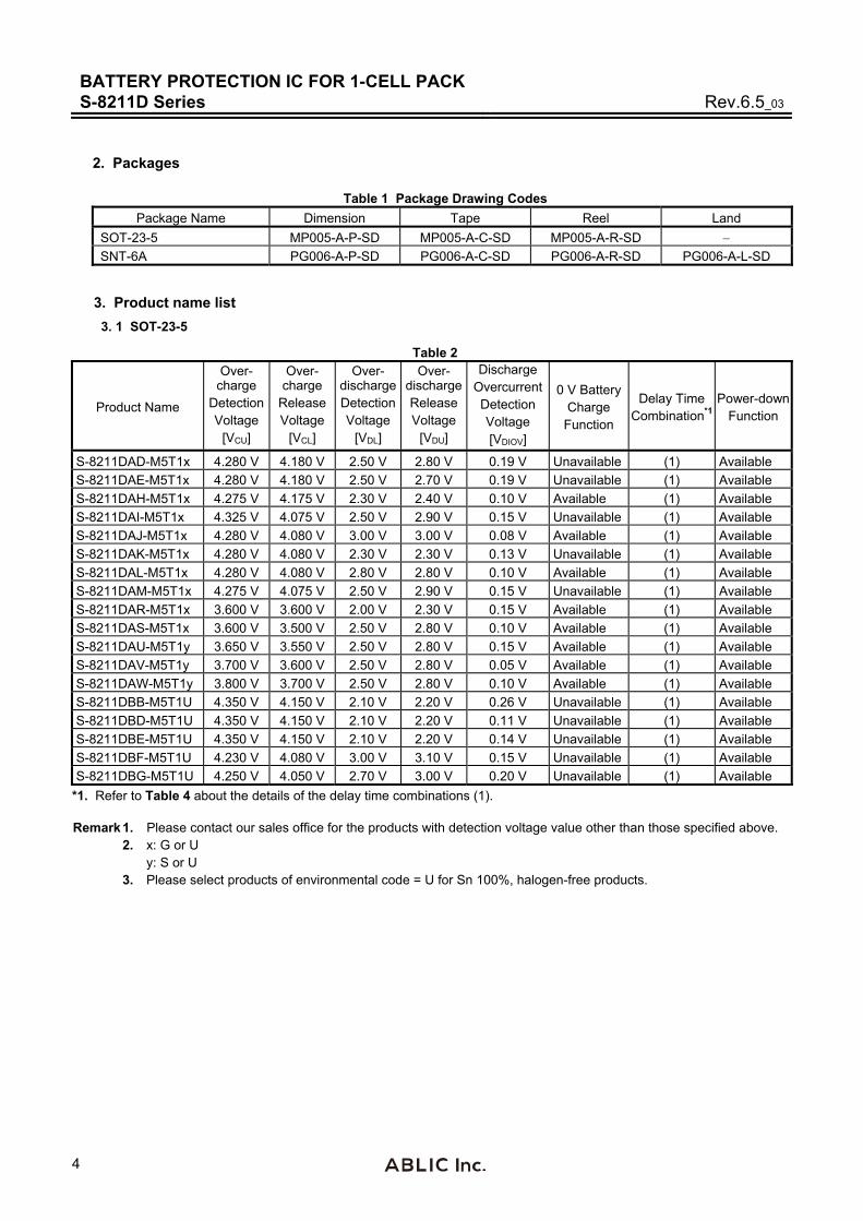
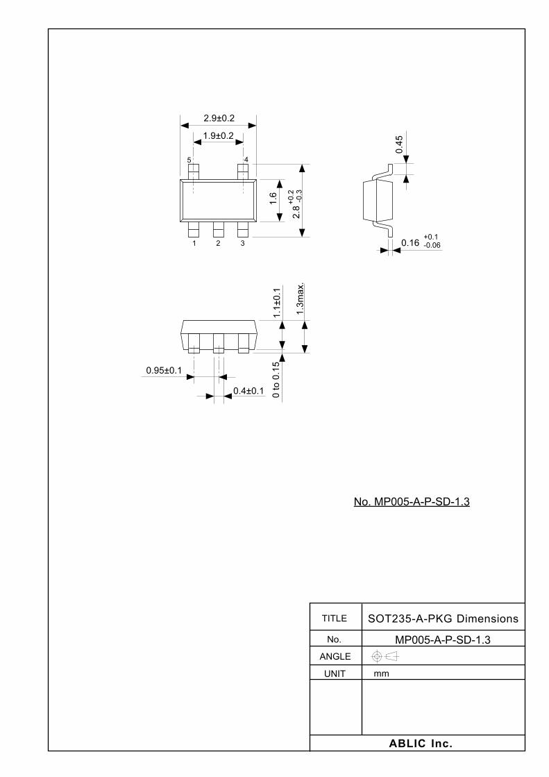
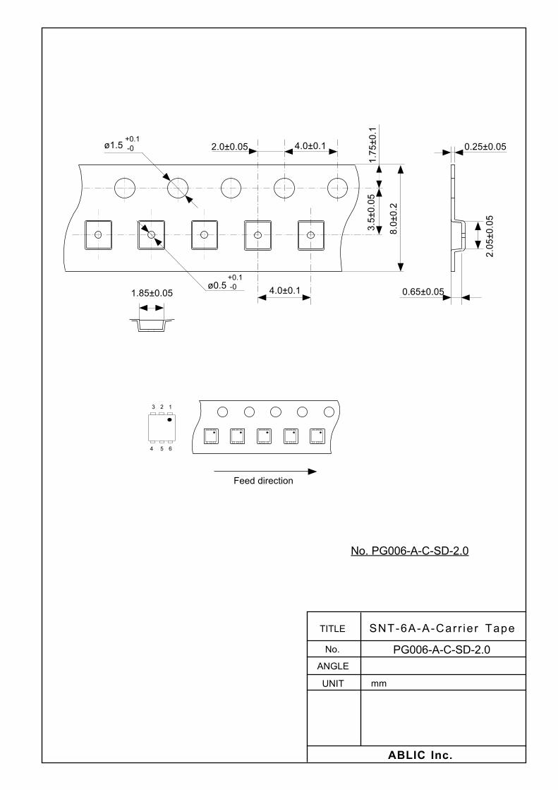
2. Packages
Table 1 Package Drawing Codes
Package Name Dimension Tape Reel Land
SOT-23-5 MP005-A-P-SD MP005-A-C-SD MP005-A-R-SD SNT-6A PG006-A-P-SD PG006-A-C-SD PG006-A-R-SD PG006-A-L-SD
3. Product name list
3. 1 SOT-23-5
Table 2
Product Name
Over-charge
DetectionVoltage
[VCU]
Over-charge
Release Voltage
[VCL]
Over-dischargeDetectionVoltage
[VDL]
Over-dischargeReleaseVoltage
[VDU]
DischargeOvercurrentDetection Voltage [VDIOV]
0 V Battery Charge
Function
Delay Time Combination*1
Power-downFunction
S-8211DAD-M5T1x 4.280 V 4.180 V 2.50 V 2.80 V 0.19 V Unavailable (1) Available
S-8211DAE-M5T1x 4.280 V 4.180 V 2.50 V 2.70 V 0.19 V Unavailable (1) Available
S-8211DAH-M5T1x 4.275 V 4.175 V 2.30 V 2.40 V 0.10 V Available (1) Available
S-8211DAI-M5T1x 4.325 V 4.075 V 2.50 V 2.90 V 0.15 V Unavailable (1) Available
S-8211DAJ-M5T1x 4.280 V 4.080 V 3.00 V 3.00 V 0.08 V Available (1) Available
S-8211DAK-M5T1x 4.280 V 4.080 V 2.30 V 2.30 V 0.13 V Unavailable (1) Available
S-8211DAL-M5T1x 4.280 V 4.080 V 2.80 V 2.80 V 0.10 V Available (1) Available
S-8211DAM-M5T1x 4.275 V 4.075 V 2.50 V 2.90 V 0.15 V Unavailable (1) Available
S-8211DAR-M5T1x 3.600 V 3.600 V 2.00 V 2.30 V 0.15 V Available (1) Available
S-8211DAS-M5T1x 3.600 V 3.500 V 2.50 V 2.80 V 0.10 V Available (1) Available
S-8211DAU-M5T1y 3.650 V 3.550 V 2.50 V 2.80 V 0.15 V Available (1) Available
S-8211DAV-M5T1y 3.700 V 3.600 V 2.50 V 2.80 V 0.05 V Available (1) Available
S-8211DAW-M5T1y 3.800 V 3.700 V 2.50 V 2.80 V 0.10 V Available (1) Available
S-8211DBB-M5T1U 4.350 V 4.150 V 2.10 V 2.20 V 0.26 V Unavailable (1) Available
S-8211DBD-M5T1U 4.350 V 4.150 V 2.10 V 2.20 V 0.11 V Unavailable (1) Available
S-8211DBE-M5T1U 4.350 V 4.150 V 2.10 V 2.20 V 0.14 V Unavailable (1) Available
S-8211DBF-M5T1U 4.230 V 4.080 V 3.00 V 3.10 V 0.15 V Unavailable (1) Available
S-8211DBG-M5T1U 4.250 V 4.050 V 2.70 V 3.00 V 0.20 V Unavailable (1) Available
*1. Refer to Table 4 about the details of the delay time combinations (1).
Remark 1. Please contact our sales office for the products with detection voltage value other than those specified above. 2. x: G or U y: S or U 3. Please select products of environmental code = U for Sn 100%, halogen-free products.

BATTERY PROTECTION IC FOR 1-CELL PACKRev.6.5_03 S-8211D Series
5
3. 2 SNT-6A
Table 3
Product Name
Over-charge
DetectionVoltage
[VCU]
Over-charge
Release Voltage
[VCL]
Over-dischargeDetectionVoltage
[VDL]
Over-dischargeReleaseVoltage
[VDU]
Discharge
Overcurrent
Detection
Voltage
[VDIOV]
0 V Battery Charge
Function
Delay Time Combination*1
Power-downFunction
S-8211DAD-I6T1U 4.280 V 4.180 V 2.50 V 2.80 V 0.19 V Unavailable (1) Available
S-8211DAE-I6T1U 4.280 V 4.180 V 2.50 V 2.70 V 0.19 V Unavailable (1) Available
S-8211DAF-I6T1U 4.250 V 4.050 V 2.40 V 2.90 V 0.10 V Available (2) Unavailable
S-8211DAG-I6T1U 4.280 V 4.080 V 2.30 V 2.30 V 0.08 V Available (1) Unavailable
S-8211DAI-I6T1U 4.325 V 4.075 V 2.50 V 2.90 V 0.15 V Unavailable (1) Available
S-8211DAN-I6T1U 4.280 V 4.080 V 2.30 V 3.00 V 0.10 V Unavailable (3) Available
S-8211DAQ-I6T1U 4.280 V 4.080 V 2.30 V 2.30 V 0.10 V Unavailable (3) Available
S-8211DAT-I6T1U 4.280 V 4.080 V 2.70 V 2.70 V 0.08 V Unavailable (3) Available
S-8211DAX-I6T1U 4.280 V 4.080 V 2.00 V 2.00 V 0.11 V Unavailable (3) Available
S-8211DAY-I6T1U 3.900 V 3.900 V 2.00 V 2.30 V 0.15 V Available (1) Available
S-8211DAZ-I6T1U 3.800 V 3.500 V 2.40 V 2.70 V 0.07 V Available (1) Available
S-8211DBA-I6T1U 4.000 V 3.900 V 2.35 V 2.65 V 0.10 V Available (1) Available
S-8211DBC-I6T1U 4.250 V 4.150 V 3.00 V 3.10 V 0.20 V Unavailable (1) Available
*1. Refer to Table 4 about the details of the delay time combinations (1) to (3).
Remark Please contact our sales office for the products with detection voltage value other than those specified above.
Table 4
Delay Time Combination
Overcharge Detection
Delay Time
[tCU]
Overdischarge Detection
Delay Time
[tDL]
Discharge Overcurrent
Detection Delay Time
[tDIOV]
Load Short-circuiting
Detection Delay Time
[tSHORT]
(1) 1.2 s 150 ms 9 ms 300 s
(2) 1.2 s 75 ms 9 ms 300 s
(3) 1.2 s 150 ms 18 ms 300 s
Remark The delay times can be changed within the range listed Table 5. For details, please contact our sales office.
Table 5
Delay Time Symbol Selection Range Remark
Overcharge detection delay time tCU 143 ms 573 ms 1.2 s*1 Select a value from the left.
Overdischarge detection delay time tDL 38 ms 150 ms*1 300 ms Select a value from the left.
Discharge overcurrent detection delay time tDIOV 4.5 ms 9 ms*1 18 ms Select a value from the left.
Load short-circuiting detection delay time tSHORT 300 s*1 560 s Select a value from the left.
*1. The value is the delay time of the standard products.

BATTERY PROTECTION IC FOR 1-CELL PACK S-8211D Series Rev.6.5_03
6
Pin Configurations
1. SOT-23-5
1 32
45
Top view
Table 6
Pin No. Symbol Description
1 VM
Voltage detection pin between VM pin and VSS pin (Overcurrent / charger detection pin)
2 VDD Input pin for positive power supply
3 VSS Input pin for negative power supply
4 DO
Connection pin of discharge control FET gate (CMOS output)
5 CO
Connection pin of charge control FET gate (CMOS output)
Figure 2
2. SNT-6A
54
623
1
Top view
Table 7
Pin No. Symbol Description
1 NC*1 No connection
2 CO Connection pin of charge control FET gate (CMOS output)
3 DO Connection pin of discharge control FET gate (CMOS output)
4 VSS Input pin for negative power supply
Figure 3 5 VDD Input pin for positive power supply
6 VM Voltage detection pin between VM pin and VSS pin (Overcurrent / charger detection pin)
*1. The NC pin is electrically open.
The NC pin can be connected to the VDD pin or the VSS pin.

BATTERY PROTECTION IC FOR 1-CELL PACKRev.6.5_03 S-8211D Series
7
Absolute Maximum Ratings
Table 8 (Ta = 25C unless otherwise specified)
Item Symbol Applied Pin Absolute Maximum Rating Unit
Input voltage between VDD pin and VSS pin
VDS VDD VSS 0.3 to VSS 12 V
VM pin input voltage VVM VM VDD 28 to VDD 0.3 V
DO pin output voltage VDO DO VSS 0.3 to VDD 0.3 V
CO pin output voltage VCO CO VVM 0.3 to VDD 0.3 V
Power dissipation SOT-23-5
PD
250 (When not mounted on board) mW
600*1 mW
SNT-6A 400*1 mW
Operation ambient temperature Topr 40 to 85 C
Storage temperature Tstg 55 to 125 C
*1. When mounted on board [Mounted board]
(1) Board size: 114.3 mm 76.2 mm t1.6 mm (2) Board name: JEDEC STANDARD51-7
Caution The absolute maximum ratings are rated values exceeding which the product could suffer physical
damage. These values must therefore not be exceeded under any conditions.
0 50 100 150
700
400
0
Pow
er D
issi
patio
n (P
D)
[mW
]
Ambient Temperature (Ta) [C]
200
600
500
300
100
SNT-6A
SOT-23-5
Figure 4 Power Dissipation of Package (When Mounted on Board)

BATTERY PROTECTION IC FOR 1-CELL PACK S-8211D Series Rev.6.5_03
8
Electrical Characteristics
1. Except detection delay time (Ta = 25C)
Table 9(Ta = 25C unless otherwise specified)
Item Symbol Condition Min. Typ. Max. Unit Test
Condi-tion
TestCircuit
DETECTION VOLTAGE
Overcharge detection voltage VCU 3.60 V to 4.50 V, adjustable
VCU 0.025
VCU VCU 0.025
V 1 1
3.60 V to 4.50 V, adjustable, Ta = 5C to 55C*1
VCU 0.03
VCU VCU 0.03
V 1 1
Overcharge release voltage VCL 3.50 V to 4.40 V, adjustable
VCL VCU VCL 0.05
VCL VCL 0.05
V 1 1
VCL = VCU VCL 0.05
VCL VCL 0.025
V 1 1
Overdischarge detection voltage VDL 2.00 V to 3.00 V, adjustable VDL 0.05
VDL VDL 0.05
V 2 2
Overdischarge release voltage VDU 2.00 V to 3.40 V, Adjustable
VDU VDL VDU 0.10
VDU VDU 0.10
V 2 2
VDU = VDL VDU 0.05
VDU VDU 0.05
V 2 2
Discharge overcurrent detection voltage VDIOV 0.05 V to 0.30 V, adjustable VDIOV 0.015
VDIOV VDIOV 0.015
V 3 2
Load short-circuiting detection voltage*2 VSHORT 0.30 0.50 0.70 V 3 2
Charger detection voltage VCHA 1.0 0.7 0.4 V 4 2
0 V BATTERY CHARGE FUNCTION
0 V battery charge starting charger voltage V0CHA 0 V battery charge function "available" 1.2 V 10 2
0 V battery charge inhibition battery voltage V0INH 0 V battery charge function "unavailable" 0.5 V 11 2
INTERNAL RESISTANCE
Resistance between VM pin and VDD pin RVMD VDD = 1.8 V, VVM = 0 V 100 300 900 k 5 3
Resistance between VM pin and VSS pin RVMS VDD = 3.5 V, VVM = 1.0 V 10 20 40 k 5 3
INPUT VOLTAGE
Operation voltage between VDD pin and VSS pin VDSOP1 1.5 8 V
Operation voltage between VDD pin and VM pin VDSOP2 1.5 28 V
INPUT CURRENT (WITH POWER-DOWN FUNTION)
Current consumption during operation IOPE VDD = 3.5 V, VVM = 0 V 1.0 3.0 5.5 A 4 2
Current consumption during power-down IPDN VDD = VVM = 1.5 V 0.2 A 4 2
INPUT CURRENT (WITHOUT POWER-DOWN FUNTION)
Current consumption during operation IOPE VDD = 3.5 V, VVM = 0 V 1.0 3.0 5.5 A 4 2
Current consumption during overdischarge IOPED VDD = VVM = 1.5 V 0.3 2.0 3.5 A 4 2
OUTPUT RESISTANCE
CO pin resistance "H" RCOH VCO = 3.0 V, VDD = 3.5 V, VVM = 0 V 2.5 5 10 k 6 4
CO pin resistance "L" RCOL VCO = 0.5 V, VDD = 4.5 V, VVM = 0 V 2.5 5 10 k 6 4
DO pin resistance "H" RDOH VDO = 3.0 V, VDD = 3.5 V, VVM = 0 V 2.5 5 10 k 7 4
DO pin resistance "L" RDOL VDO = 0.5 V, VDD = VVM = 1.8 V 2.5 5 10 k 7 4
*1. Since products are not screened at high and low temperature, the specification for this temperature range is guaranteed by design, not tested in production.
*2. In any conditions, load short-circuiting detection voltage (VSHORT) is higher than discharge overcurrent detection voltage (VDIOV).
BATTERY PROTECTION IC FOR 1-CELL PACKRev.6.5_03 S-8211D Series
9
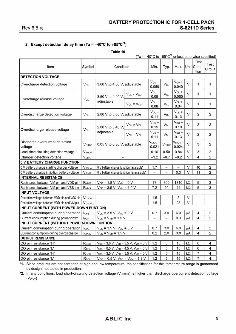
2. Except detection delay time (Ta = 40°C to 85°C*1)
Table 10(Ta = 40°C to 85°C*1 unless otherwise specified)
Item Symbol Condition Min. Typ. Max. Unit Test
Condi-tion
TestCircuit
DETECTION VOLTAGE
Overcharge detection voltage VCU 3.60 V to 4.50 V, adjustable VCU 0.060
VCU VCU 0.040
V 1 1
Overcharge release voltage VCL 3.50 V to 4.40 V, adjustable
VCL VCU VCL 0.08
VCL VCL 0.065
V 1 1
VCL = VCU VCL 0.08
VCL VCL 0.04
V 1 1
Overdischarge detection voltage VDL 2.00 V to 3.00 V, adjustable VDL 0.11
VDL VDL 0.13
V 2 2
Overdischarge release voltage VDU 2.00 V to 3.40 V, adjustable
VDU VDL VDU 0.15
VDU VDU 0.19
V 2 2
VDU = VDL VDU 0.11
VDU VDU 0.13
V 2 2
Discharge overcurrent detection voltage
VDIOV 0.05 V to 0.30 V, adjustable VDIOV 0.021
VDIOV VDIOV 0.024
V 3 2
Load short-circuiting detection voltage*2 VSHORT 0.16 0.50 0.84 V 3 2
Charger detection voltage VCHA 1.2 0.7 0.2 V 4 2
0 V BATTERY CHARGE FUNCTION
0 V battery charge starting charger voltage V0CHA 0 V battery charge function "available" 1.7 V 10 2
0 V battery charge inhibition battery voltage V0INH 0 V battery charge function "unavailable" 0.3 V 11 2
INTERNAL RESISTANCE
Resistance between VM pin and VDD pin RVMD VDD = 1.8 V, VVM = 0 V 78 300 1310 k 5 3
Resistance between VM pin and VSS pin RVMS VDD = 3.5 V, VVM = 1.0 V 7.2 20 44 k 5 3
INPUT VOLTAGE
Operation voltage between VDD pin and VSS pin VDSOP1 1.5 8 V
Operation voltage between VDD pin and VM pin VDSOP2 1.5 28 V
INPUT CURRENT (WITH POWER-DOWN FUNTION)
Current consumption during operation IOPE VDD = 3.5 V, VVM = 0 V 0.7 3.0 6.0 A 4 2
Current consumption during power-down IPDN VDD = VVM = 1.5 V 0.3 A 4 2
INPUT CURRENT (WITHOUT POWER-DOWN FUNTION)
Current consumption during operation IOPE VDD = 3.5 V, VVM = 0 V 0.7 3.0 6.0 A 4 2
Current consumption during overdischarge IOPED VDD = VVM = 1.5 V 0.2 2.0 3.8 A 4 2
OUTPUT RESISTANCE
CO pin resistance "H" RCOH VCO = 3.0 V, VDD = 3.5 V, VVM = 0 V 1.2 5 15 k 6 4
CO pin resistance "L" RCOL VCO = 0.5 V, VDD = 4.5 V, VVM = 0 V 1.2 5 15 k 6 4
DO pin resistance "H" RDOH VDO = 3.0 V, VDD = 3.5 V, VVM = 0 V 1.2 5 15 k 7 4
DO pin resistance "L" RDOL VDO = 0.5 V, VDD = VVM = 1.8 V 1.2 5 15 k 7 4
*1. Since products are not screened at high and low temperature, the specification for this temperature range is guaranteed by design, not tested in production.
*2. In any conditions, load short-circuiting detection voltage (VSHORT) is higher than discharge overcurrent detection voltage (VDIOV).
BATTERY PROTECTION IC FOR 1-CELL PACK S-8211D Series Rev.6.5_03
10
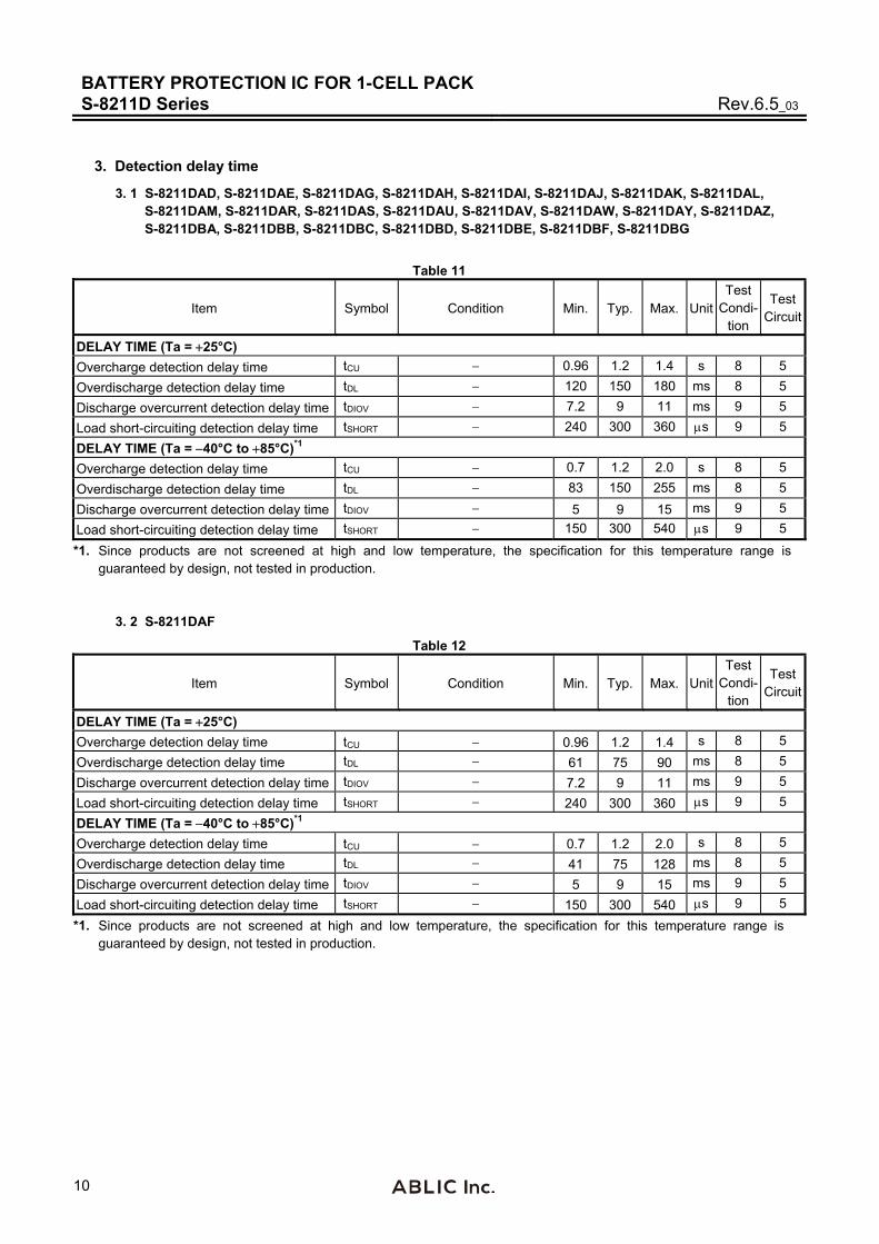
3. Detection delay time
3. 1 S-8211DAD, S-8211DAE, S-8211DAG, S-8211DAH, S-8211DAI, S-8211DAJ, S-8211DAK, S-8211DAL, S-8211DAM, S-8211DAR, S-8211DAS, S-8211DAU, S-8211DAV, S-8211DAW, S-8211DAY, S-8211DAZ, S-8211DBA, S-8211DBB, S-8211DBC, S-8211DBD, S-8211DBE, S-8211DBF, S-8211DBG
Table 11
Item Symbol Condition Min. Typ. Max. Unit Test
Condi-tion
TestCircuit
DELAY TIME (Ta = 25°C)
Overcharge detection delay time tCU 0.96 1.2 1.4 s 8 5
Overdischarge detection delay time tDL 120 150 180 ms 8 5
Discharge overcurrent detection delay time tDIOV 7.2 9 11 ms 9 5
Load short-circuiting detection delay time tSHORT 240 300 360 s 9 5
DELAY TIME (Ta = 40°C to 85°C)*1
Overcharge detection delay time tCU 0.7 1.2 2.0 s 8 5
Overdischarge detection delay time tDL 83 150 255 ms 8 5
Discharge overcurrent detection delay time tDIOV 5 9 15 ms 9 5
Load short-circuiting detection delay time tSHORT 150 300 540 s 9 5
*1. Since products are not screened at high and low temperature, the specification for this temperature range is guaranteed by design, not tested in production.
3. 2 S-8211DAF
Table 12
Item Symbol Condition Min. Typ. Max. Unit Test
Condi-tion
TestCircuit
DELAY TIME (Ta = 25°C)
Overcharge detection delay time tCU 0.96 1.2 1.4 s 8 5
Overdischarge detection delay time tDL 61 75 90 ms 8 5
Discharge overcurrent detection delay time tDIOV 7.2 9 11 ms 9 5
Load short-circuiting detection delay time tSHORT 240 300 360 s 9 5
DELAY TIME (Ta = 40°C to 85°C)*1
Overcharge detection delay time tCU 0.7 1.2 2.0 s 8 5
Overdischarge detection delay time tDL 41 75 128 ms 8 5
Discharge overcurrent detection delay time tDIOV 5 9 15 ms 9 5
Load short-circuiting detection delay time tSHORT 150 300 540 s 9 5
*1. Since products are not screened at high and low temperature, the specification for this temperature range is guaranteed by design, not tested in production.
BATTERY PROTECTION IC FOR 1-CELL PACKRev.6.5_03 S-8211D Series
11
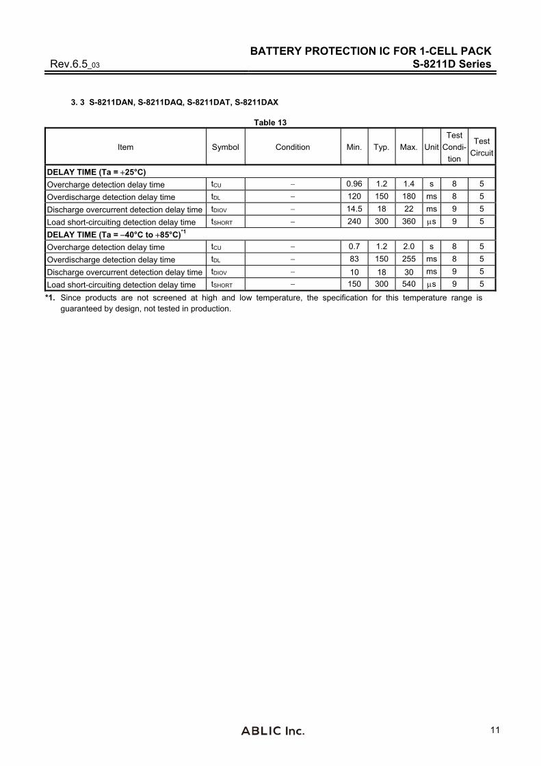
3. 3 S-8211DAN, S-8211DAQ, S-8211DAT, S-8211DAX
Table 13
Item Symbol Condition Min. Typ. Max. Unit
Test
Condi-
tion
Test
Circuit
DELAY TIME (Ta = 25°C)
Overcharge detection delay time tCU 0.96 1.2 1.4 s 8 5
Overdischarge detection delay time tDL 120 150 180 ms 8 5
Discharge overcurrent detection delay time tDIOV 14.5 18 22 ms 9 5
Load short-circuiting detection delay time tSHORT 240 300 360 s 9 5
DELAY TIME (Ta = 40°C to 85°C)*1
Overcharge detection delay time tCU 0.7 1.2 2.0 s 8 5
Overdischarge detection delay time tDL 83 150 255 ms 8 5
Discharge overcurrent detection delay time tDIOV 10 18 30 ms 9 5
Load short-circuiting detection delay time tSHORT 150 300 540 s 9 5
*1. Since products are not screened at high and low temperature, the specification for this temperature range is guaranteed by design, not tested in production.

BATTERY PROTECTION IC FOR 1-CELL PACK S-8211D Series Rev.6.5_03
12
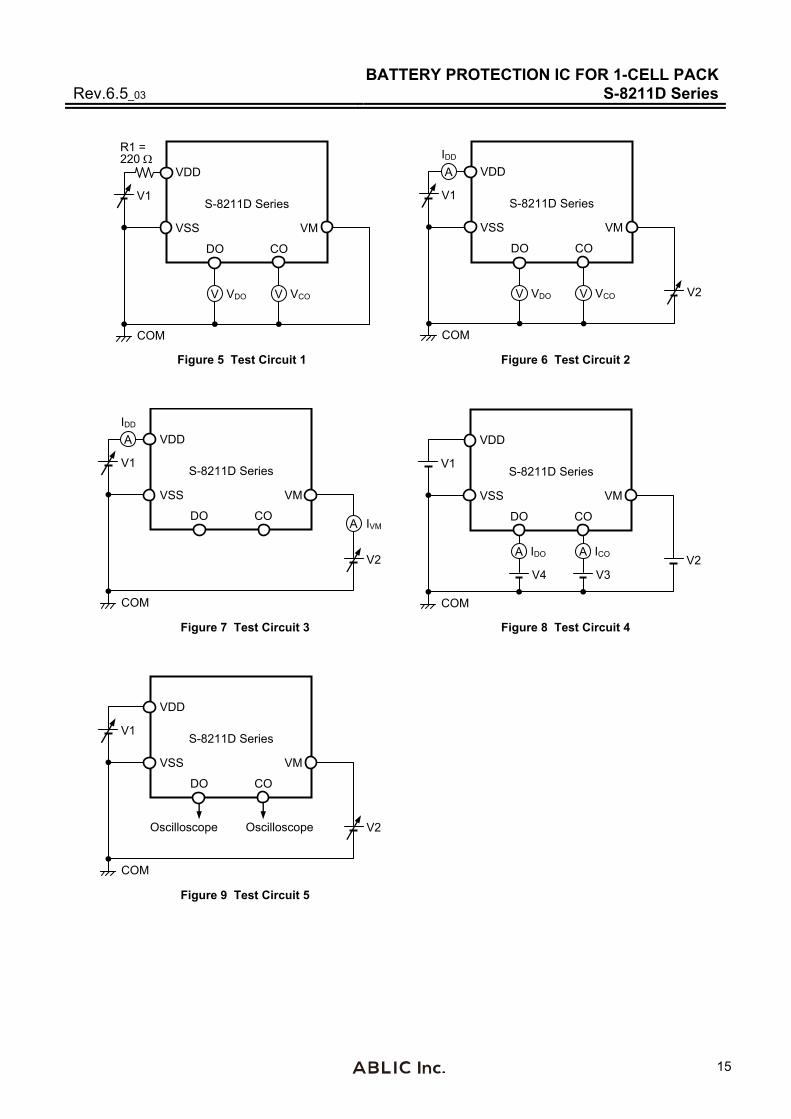
Test Circuits
Caution Unless otherwise specified, the output voltage levels "H" and "L" at the CO pin (VCO) and the DO pin (VDO) are judged by the threshold voltage (1.0 V) of the N-channel FET. Judge the CO pin level with respect to VVM and the DO pin level with respect to VSS.
1. Overcharge detection voltage, overcharge release voltage
(Test condition 1, test circuit 1)
Overcharge detection voltage (VCU) is defined as the voltage between the VDD pin and the VSS pin at which VCO goes from "H" to "L" when the voltage V1 is gradually increased from the starting condition of V1 = 3.5 V. Overcharge release voltage (VCL) is defined as the voltage between the VDD pin and the VSS pin at which VCO goes from "L" to "H" when the voltage V1 is then gradually decreased. Overcharge hysteresis voltage (VHC) is defined as the difference between overcharge detection voltage (VCU) and overcharge release voltage (VCL).
2. Overdischarge detection voltage, overdischarge release voltage
(Test condition 2, test circuit 2)
Overdischarge detection voltage (VDL) is defined as the voltage between the VDD pin and the VSS pin at which VDO goes from "H" to "L" when the voltage V1 is gradually decreased from the starting condition of V1 = 3.5 V, V2 = 0 V. Overdischarge release voltage (VDU) is defined as the voltage between the VDD pin and the VSS pin at which VDO goes from "L" to "H" when the voltage V1 is then gradually increased. Overdischarge hysteresis voltage (VHD) is defined as the difference between overdischarge release voltage (VDU) and overdischarge detection voltage (VDL).
3. Discharge overcurrent detection voltage
(Test condition 3, test circuit 2)
Discharge overcurrent detection voltage (VDIOV) is defined as the voltage between the VM pin and the VSS pin whose delay time for changing VDO from "H" to "L" lies between the minimum and the maximum value of discharge overcurrent delay time when the voltage V2 is increased rapidly (within 10 s) from the starting condition of V1 = 3.5 V, V2 = 0 V.
4. Load short-circuiting detection voltage
(Test condition 3, test circuit 2)
Load short-circuiting detection voltage (VSHORT) is defined as the voltage between the VM pin and the VSS pin whose delay time for changing VDO from "H" to "L" lies between the minimum and the maximum value of load short-circuiting delay time when the voltage V2 is increased rapidly (within 10 s) from the starting condition of V1 = 3.5 V, V2 = 0 V.
5. Current consumption during operation
(Test condition 4, test circuit 2)
The current consumption during operation (IOPE) is the current that flows through the VDD pin (IDD) under the set conditions of V1 = 3.5 V and V2 = 0 V (normal status).
6. Charger detection voltage (= abnormal charge current detection voltage)
(Test condition 4, test circuit 2)
The charger detection voltage (VCHA) is the voltage between the VM pin and the VSS pin; when gradually increasing V1 at V1 = 1.8 V, V2 = 0 V to set V1 = VDL (VHD/2), after that, decreasing V2 gradually from 0 V so that VDO goes "L" to "H". Measurement of the charger detection voltage is available for the product with overdischarge hysteresis VHD 0 only. The abnormal charge current detection voltage is the voltage between the VM pin and the VSS pin; when gradually decreasing V2 at V1 = 3.5 V, V2 = 0 V and VCO goes "H" to "L". The value of the abnormal charge current detection voltage is equal to the charger detection voltage (VCHA).

BATTERY PROTECTION IC FOR 1-CELL PACKRev.6.5_03 S-8211D Series
13
7. Current consumption during power-down, current consumption during overdischarge
(Test condition 4, test circuit 2)
7. 1 With power-down function
The current consumption during power-down (IPDN) is the current that flows through the VDD pin (IDD) under the set conditions of V1 = V2 = 1.5 V (overdischarge status).
7. 2 Without power-down function
The current consumption during overdischarge (IOPED) is the current that flows through the VDD pin (IDD) under the set conditions of V1 = V2 = 1.5 V (overdischarge status).
8. Resistance between VM pin and VDD pin
(Test condition 5, test circuit 3)
The resistance between the VM pin and the VDD pin (RVMD) is the resistance between the VM pin and the VDD pin under the set conditions of V1 = 1.8 V, V2 = 0 V.
9. Resistance between VM pin and VSS pin
(Test condition 5, test circuit 3)
The resistance between the VM pin and the VSS pin (RVMS) is the resistance between the VM pin and the VSS pin under the set conditions of V1 = 3.5 V, V2 = 1.0 V.
10. CO pin resistance "H"
(Test condition 6, test circuit 4)
The CO pin resistance "H" (RCOH) is the resistance at the CO pin under the set conditions of V1 = 3.5 V, V2 = 0 V, V3 = 3.0 V.
11. CO pin resistance "L" (Test condition 6, test circuit 4)
The CO pin resistance "L" (RCOL) is the resistance at the CO pin under the set conditions of V1 = 4.5 V, V2 = 0 V, V3 = 0.5 V.
12. DO pin resistance "H" (Test condition 7, test circuit 4)
The DO pin resistance "H" (RDOH) is the resistance at the DO pin under the set conditions of V1 = 3.5 V, V2 = 0 V, V4 = 3.0 V.
13. DO pin resistance "L" (Test condition 7, test circuit 4)
The DO pin resistance "L" (RDOL) is the resistance at the DO pin under the set conditions of V1 = 1.8 V, V2 = 0 V, V4 = 0.5 V.
14. Overcharge detection delay time (Test condition 8, test circuit 5)
The overcharge detection delay time (tCU) is the time needed for VCO to change from "H" to "L" just after the voltage V1 momentarily increases (within 10 s) from overcharge detection voltage (VCU) 0.2 V to overcharge detection voltage (VCU) 0.2 V under the set conditions of V2 = 0 V.
15. Overdischarge detection delay tme
(Test condition 8, test circuit 5)
The overdischarge detection delay time (tDL) is the time needed for VDO to change from "H" to "L" just after the voltage V1 momentarily decreases (within 10 s) from overdischarge detection voltage (VDL) 0.2 V to overdischarge detection voltage (VDL) 0.2 V under the set condition of V2 = 0 V.

BATTERY PROTECTION IC FOR 1-CELL PACK S-8211D Series Rev.6.5_03
14
16. Discharge overcurrent detection delay time
(Test condition 9, test circuit 5)
Discharge overcurrent detection delay time (tDIOV) is the time needed for VDO to go to "L" after the voltage V2 momentarily increases (within 10 s) from 0 V to 0.35 V under the set conditions of V1 = 3.5 V, V2 = 0 V.
17. Load short-circuiting detection delay time
(Test condition 9, test circuit 5)
Load short-circuiting detection delay time (tSHORT) is the time needed for VDO to go to "L" after the voltage V2 momentarily increases (within 10 s) from 0 V to 1.6 V under the set conditions of V1 = 3.5 V, V2 = 0 V.
18. 0 V battery charge starting charger voltage (0 V battery charge function "available")
(Test condition 10, test circuit 2)
The 0 V battery charge starting charger voltage (V0CHA) is defined as the voltage between the VDD pin and the VM pin at which VCO goes to "H" (VVM 0.1 V or higher) when the voltage V2 is gradually decreased from the starting condition of V1 = V2 = 0 V.
19. 0 V battery charge inhibition battery voltage (0 V battery charge function "unavailable")
(Test condition 11, test circuit 2)
The 0 V battery charge inhibition battery voltage (V0INH) is defined as the voltage between the VDD pin and the VSS pin at which VCO goes to "H" (VVM 0.1 V or higher) when the voltage V1 is gradually increased from the starting condition of V1 = 0 V, V2 = 4 V.
BATTERY PROTECTION IC FOR 1-CELL PACKRev.6.5_03 S-8211D Series
15
V VDO V VCO
CO DO
VSS
VDD
VM
S-8211D Series
R1 = 220
V1
COM
V VDO V VCO
CO DO
VSS
VDD
VM
S-8211D Series V1
V2
COM
A
IDD
Figure 5 Test Circuit 1 Figure 6 Test Circuit 2
CO DO
VSS
VDD
VM
S-8211D Series V1
V2
COM
A
IDD
A IVM
A IDO A ICO
CO DO
VSS
VDD
VM
S-8211D Series V1
V2
COM
V4 V3
Figure 7 Test Circuit 3 Figure 8 Test Circuit 4
CO DO
VSS
VDD
VM
S-8211D Series V1
V2
COM
Oscilloscope Oscilloscope
Figure 9 Test Circuit 5
BATTERY PROTECTION IC FOR 1-CELL PACK S-8211D Series Rev.6.5_03
16
Operation
Remark Refer to the " Battery Protection IC Connection Example".
1. Normal status
The S-8211D Series monitors the voltage of the battery connected between the VDD pin and the VSS pin and the voltage difference between the VM pin and the VSS pin to control charging and discharging. When the battery voltage is in the range from overdischarge detection voltage (VDL) to overcharge detection voltage (VCU), and the VM pin voltage is not more than the discharge overcurrent detection voltage (VDIOV), the S-8211D Series turns both the charging and discharging control FETs on. This condition is called the normal status, and in this condition charging and discharging can be carried out freely. The resistance (RVMD) between the VM pin and the VDD pin, and the resistance (RVMS) between the VM pin and the VSS pin are not connected in the normal status.
Caution When the battery is connected for the first time, discharging may not be enabled. In this case, short
the VM pin and the VSS pin, or set the VM pin’s voltage at the level of the charger detection voltage (VCHA) or more and the discharge overcurrent detection voltage (VDIOV) or less by connecting the charger. The S-8211D Series then returns to the normal status.
2. Overcharge status
When the battery voltage becomes higher than overcharge detection voltage (VCU) during charging in the normal status and detection continues for the overcharge detection delay time (tCU) or longer, the S-8211D Series turns the charging control FET off to stop charging. This condition is called the overcharge status. The resistance (RVMD) between the VM pin and the VDD pin, and the resistance (RVMS) between the VM pin and the VSS pin are not connected in the overcharge status. The overcharge status is released in the following two cases ( (1) and (2) ).
(1) In the case that the VM pin voltage is higher than or equal to charger detection voltage (VCHA), and is lower than
the discharge overcurrent detection voltage (VDIOV), the S-8211D Series releases the overcharge status when the battery voltage falls below the overcharge release voltage (VCL).
(2) In the case that the VM pin voltage is higher than or equal to the discharge overcurrent detection voltage (VDIOV), the S-8211D Series releases the overcharge status when the battery voltage falls below the overcharge detection voltage (VCU).
When the discharge is started by connecting a load after the overcharge detection, the VM pin voltage rises more than the voltage at the VSS pin due to the Vf voltage of the parasitic diode. This is because the discharge current flows through the parasitic diode in the charging control FET. If the VM pin voltage is higher than or equal to the discharge overcurrent detection voltage (VDIOV), the S-8211D Series releases the overcharge status when the battery voltage is lower than or equal to the overcharge detection voltage (VCU).
Caution 1. If the battery is charged to a voltage higher than overcharge detection voltage (VCU) and the
battery voltage does not fall below overcharge detection voltage (VCU) even when a heavy load is connected, discharge overcurrent detection and load short-circuiting detection do not function until the battery voltage falls below overcharge detection voltage (VCU). Since an actual battery has an internal impedance of tens of m, the battery voltage drops immediately after a heavy load that causes overcurrent is connected, and discharge overcurrent detection and load short-circuiting detection function.
2. When a charger is connected after overcharge detection, the overcharge status is not released even if the battery voltage is below overcharge release voltage (VCL). The overcharge status is released when the VM pin voltage goes over charger detection voltage (VCHA) by removing the charger.
BATTERY PROTECTION IC FOR 1-CELL PACKRev.6.5_03 S-8211D Series
17
3. Overdischarge status
3. 1 With power-down function
When the battery voltage falls below overdischarge detection voltage (VDL) during discharging in the normal status and the detection continues for the overdischarge detection delay time (tDL) or longer, the S-8211D Series turns the discharging control FET off to stop discharging. This condition is called the overdischarge status. Under the overdischarge status, the VM pin voltage is pulled up by the resistor between the VM pin and the VDD pin in the S-8211D Series (RVMD). When voltage difference between the VM pin and the VDD pin then is 1.3 V typ. or lower, the current consumption is reduced to the power-down current consumption (IPDN). This condition is called the power-down status. The resistance (RVMS) between the VM pin and the VSS pin is not connected in the power-down status and the overdischarge status. The power-down status is released when a charger is connected and the voltage difference between the VM pin and the VDD pin becomes 1.3 V typ. or higher. When a battery in the overdischarge status is connected to a charger and provided that the VM pin voltage is lower than charger detection voltage (VCHA), the S-8211D Series releases the overdischarge status and turns the discharging FET on when the battery voltage reaches overdischarge detection voltage (VDL) or higher. When a battery in the overdischarge status is connected to a charger and provided that the VM pin voltage is not lower than charger detection voltage (VCHA), the S-8211D Series releases the overdischarge status when the battery voltage reaches overdischarge release voltage (VDU) or higher.
3. 2 Without power-down function
When the battery voltage falls below overdischarge detection voltage (VDL) during discharging in the normal status and the detection continues for the overdischarge detection delay time (tDL) or longer, the S-8211D Series turns the discharging control FET off to stop discharging. This condition is called the overdischarge status. Under the overdischarge status, the VM pin voltage is pulled up by the resistor between the VM pin and the VDD pin in the S-8211D Series (RVMD). The resistance (RVMS) between the VM pin and the VSS pin is not connected in the overdischarge status. When a battery in the overdischarge status is connected to a charger and provided that the VM pin voltage is lower than charger detection voltage (VCHA), the S-8211D Series releases the overdischarge status and turns the discharging FET on when the battery voltage reaches overdischarge detection voltage (VDL) or higher. When a battery in the overdischarge status is connected to a charger and provided that the VM pin voltage is not lower than charger detection voltage (VCHA), the S-8211D Series releases the overdischarge status when the battery voltage reaches overdischarge release voltage (VDU) or higher.
4. Discharge overcurrent status (discharge overcurrent, load short-circuiting)
When a battery in the normal status is in the status where the voltage of the VM pin is equal to or higher than the discharge overcurrent detection voltage because the discharge current is higher than the specified value and the status lasts for the discharge overcurrent detection delay time, the discharge control FET is turned off and discharging is stopped. This status is called the discharge overcurrent status. In the discharge overcurrent status, the VM pin and the VSS pin are shorted by the resistor between the VM pin and the VSS pin (RVMS) in the S-8211D Series. However, the voltage of the VM pin is at the VDD potential due to the load as long as the load is connected. When the load is disconnected completely, the VM pin returns to the VSS potential. If the S-8211D Series detects that the voltage of the VM pin returns to discharge overcurrent detection voltage (VDIOV) or lower, the discharge overcurrent status is restored to the normal status. The S-8211D Series will be restored to the normal status from discharge overcurrent detection status even when the voltage of the VM pin becomes the discharge overcurrent detection voltage (VDIOV) or lower by connecting the charger. The resistance (RVMD) between the VM pin and the VDD pin is not connected in the discharge overcurrent status.
BATTERY PROTECTION IC FOR 1-CELL PACK S-8211D Series Rev.6.5_03
18
5. Abnormal charge current detection
During charging a battery which is in the normal status, if the VM pin voltage becomes lower than the charger detection voltage (VCHA) and this status is held longer than the overcharge detection delay time (tCU), the S-8211D Series turns off the charge-control FET to stop charging. This is abnormal charge current detection. This function works in the case that the DO pin voltage is in "H", and the VM pin voltage becomes lower than the charger detection voltage (VCHA). Thus if the abnormal charge current flows in the battery in the overdischarge status, the S-8211D Series turns off the charge-control FET to stop charging; the DO pin voltage goes in "H" so that the battery voltage becomes higher than the overdischarge detection voltage (VDL), and after the overcharge detection delay time (tcu). The status of abnormal charge current detection is released by the lower potential difference between the VM pin and the VSS pin than the charger detection voltage (VCHA).
6. 0 V battery charge function "available"
This function is used to recharge a connected battery whose voltage is 0 V due to self-discharge. When the 0 V battery charge starting charger voltage (V0CHA) or a higher voltage is applied between the EB pin and EB pin by connecting a charger, the charging control FET gate is fixed to the VDD pin voltage. When the voltage between the gate and source of the charging control FET becomes equal to or higher than the turn-on voltage due to the charger voltage, the charging control FET is turned on to start charging. At this time, the discharging control FET is off and the charging current flows through the internal parasitic diode in the discharging control FET. When the battery voltage becomes equal to or higher than overdischarge release voltage (VDU), the S-8211D Series enters the normal status.
Caution Some battery providers do not recommend charging for a completely self-discharged battery. Please
ask the battery provider to determine whether to enable or inhibit the 0 V battery charge function.
7. 0 V battery charge function "unavailable"
This function inhibits recharging when a battery that is internally short-circuited (0 V battery) is connected. When the battery voltage is the 0 V battery charge inhibition battery voltage (V0INH) or lower, the charging control FET gate is fixed to the EB pin voltage to inhibit charging. When the battery voltage is the 0 V battery charge inhibition battery voltage (V0INH) or higher, charging can be performed.
Caution Some battery providers do not recommend charging for a completely self-discharged battery. Please
ask the battery provider to determine whether to enable or inhibit the 0 V battery charge function.

BATTERY PROTECTION IC FOR 1-CELL PACKRev.6.5_03 S-8211D Series
19
8. Delay circuit
The detection delay times are determined by dividing a clock of approximately 3.5 kHz by the counter.
Remark1. The discharge overcurrent detection delay time (tDIOV) and the load short-circuiting detection delay time (tSHORT) start when the discharge overcurrent detection voltage (VDIOV) is detected. When the load short-circuiting detection voltage (VSHORT) is detected over the load short-circuiting detection delay time (tSHORT) after the detection of discharge overcurrent detection voltage (VDIOV), the S-8211D Series turns the discharging control FET off within tSHORT from the time of detecting VSHORT.
DO pin
VM pin
VDD
VDD
Time
VDIOV
VSS
VSS
VSHORT
Load short-circuiting detection delay time (tSHORT)
Time
tD 0 tD tSHORT
Figure 10
2. With power-down function
When any overcurrent is detected and the overcurrent continues for longer than the overdischarge detection delay time (tDL) without the load being released, the status changes to the power-down status at the point where the battery voltage falls below overdischarge detection voltage (VDL). When the battery voltage falls below overdischarge detection voltage (VDL) due to overcurrent, the S-8211D Series turns the discharging control FET off via overcurrent detection. In this case, if the recovery of the battery voltage is so slow that the battery voltage after the overdischarge detection delay time (tDL) is still lower than the overdischarge detection voltage (VDL), the S-8211D Series shifts to the power-down status. Without power-down function
When any overcurrent is detected and the overcurrent continues for longer than the overdischarge detection delay time (tDL) without the load being released, the status changes to the overdischarge status at the point where the battery voltage falls below overdischarge detection voltage (VDL). When the battery voltage falls below overdischarge detection voltage (VDL) due to overcurrent, the S-8211D Series turns the discharging control FET off via overcurrent detection. In this case, if the recovery of the battery voltage is so slow that the battery voltage after the overdischarge detection delay time (tDL) is still lower than the overdischarge detection voltage (VDL), the S-8211D Series shifts to the overdischarge status.

BATTERY PROTECTION IC FOR 1-CELL PACK S-8211D Series Rev.6.5_03
20
Timing Chart
1. Overcharge detection, overdischarge detection
VCU
VDU (VDL VHD) VDL
VCL (VCU VHC)
Battery voltage
VSS
CO pin voltage
VDD DO pin voltage
VSS
Charger connection
Load connection
Status*1
Overcharge detection delay time (tCU) Overdischarge detection delay time (tDL)
(1) (2) (1) (3) (1)
VDIOV VSS
VM pin voltage
VDD
VEB
VDD
VEB
*1. (1): Normal status (2): Overcharge status (3): Overdischarge status Remark The charger is assumed to charge with a constant current.
Figure 11

BATTERY PROTECTION IC FOR 1-CELL PACKRev.6.5_03 S-8211D Series
21
2. Discharge overcurrent detection
VDD
VSS
VSHORT
(1) (2) (1) (1)
Load short-circuiting detection delay time (tSHORT)
(2)
VDIOV
Discharge overcurrent detection delay time (tDIOV)
VCU
VDU (VDL VHD) VDL
VCL (VCU VHC)
Battery voltage
VSS
CO pin voltage
VDD
DO pin voltage
VSS
Load connection
Status *1
VM pin voltage
VDD
*1. (1): Normal status (2): Discharge overcurrent status Remark The charger is assumed to charge with a constant current.
Figure 12
BATTERY PROTECTION IC FOR 1-CELL PACK S-8211D Series Rev.6.5_03
22
3. Charger detection
VDD DO pin voltage
VSS
VDD
VSS
CO pin voltage
VDD
VSS
VM pin voltage
VCHA
VCU
VDU (VDL VHD) VDL
VCL (VCU VHC) Battery voltage
Status*1
Load connection
Overdischarge detection delay time (tDL)
(1)
In case VM pin voltage < VCHA Overdischarge is released at the overdischarge detection voltage (VDL)
Charger connection
(2)(1)
*1. (1): Normal status (2): Overdischarge status Remark The charger is assumed to charge with a constant current.
Figure 13

BATTERY PROTECTION IC FOR 1-CELL PACKRev.6.5_03 S-8211D Series
23
4. Abnormal charge current detection
VDD
DO pin voltage
VSS
VDD
VSS
CO pin voltage
VDD
VSS
VM pin voltage
VCHA
VCU
VDU (VDL VHD) VDL
VCL (VCU VHC) Battery voltage
Charger connection
Abnormal charge current detection delay time ( = overcharge detection delay time (tCU))
Status*1
Load connection
Overdischarge detectiondelay time (tDL)
(1)(2) (3) (1) (1)
*1. (1): Normal status (2): Overdischarge status (3): Overcharge status Remark The charger is assumed to charge with a constant current.
Figure 14

BATTERY PROTECTION IC FOR 1-CELL PACK S-8211D Series Rev.6.5_03
24
Battery Protection IC Connection Example
R1
Battery C1
VSS DO
VDD
CO VM
S-8211D Series
FET1 FET2
EB
EB
R2
Figure 15
Table 14 Constants for External Components
Symbol Part Purpose Min. Typ. Max. Remark
FET1 N-channel MOS FET
Discharge control
Threshold voltage Overdischarge detection voltage*1 Gate to source withstand voltage Charger voltage*2
FET2 N-channel MOS FET
Charge control
Threshold voltage Overdischarge detection voltage*1 Gate to source withstand voltage Charger voltage*2
R1 Resistor ESD protection, For power fluctuation
100 220 330 Resistance should be as small as possible to avoid lowering the overcharge detection accuracy due to current consumption.*3
C1 Capacitor For power fluctuation 0.022 F 0.1 F 1.0 F Connect a capacitor of 0.022 F or higher between VDD pin and VSS pin.*4
R2 Resistor Protection for reverse connection of a charger
300 2 k 4 k Select as large a resistance as possible to prevent current when a charger is connected in reverse.*5
*1. If the threshold voltage of a FET is low, the FET may not cut the charge current. If a FET with a threshold voltage equal to or higher than the overdischarge detection voltage is used, discharging may be stopped before overdischarge is detected.
*2. If the withstand voltage between the gate and source is lower than the charger voltage, the FET may be destroyed. *3. If a high resistor is connected to R1, the voltage between the VDD pin and the VSS pin may exceed the absolute
maximum rating when a charger is connected in reverse since the current flows from the charger to the IC. Insert a resistor of 100 or higher as R1 for ESD protection.
*4. If a capacitor of less than 0.022 F is connected to C1, the DO pin may oscillate when load short-circuiting is detected. Be sure to connect a capacitor of 0.022 F or higher to C1.
*5. If a resistor of 4 k or higher is connected to R2, the charging current may not be cut when a high-voltage charger is connected.
Caution 1. The above constants may be changed without notice.
2. It has not been confirmed whether the operation is normal or not in circuits other than the above example of connection. In addition, the example of connection shown above and the constant do not guarantee proper operation. Perform thorough evaluation using the actual application to set the constant.
BATTERY PROTECTION IC FOR 1-CELL PACKRev.6.5_03 S-8211D Series
25
Precautions
The application conditions for the input voltage, output voltage, and load current should not exceed the package power dissipation.
Do not apply an electrostatic discharge to this IC that exceeds the performance ratings of the built-in electrostatic protection circuit.
ABLIC Inc. claims no responsibility for any and all disputes arising out of or in connection with any infringement by products including this IC of patents owned by a third party.
BATTERY PROTECTION IC FOR 1-CELL PACK S-8211D Series Rev.6.5_03
26
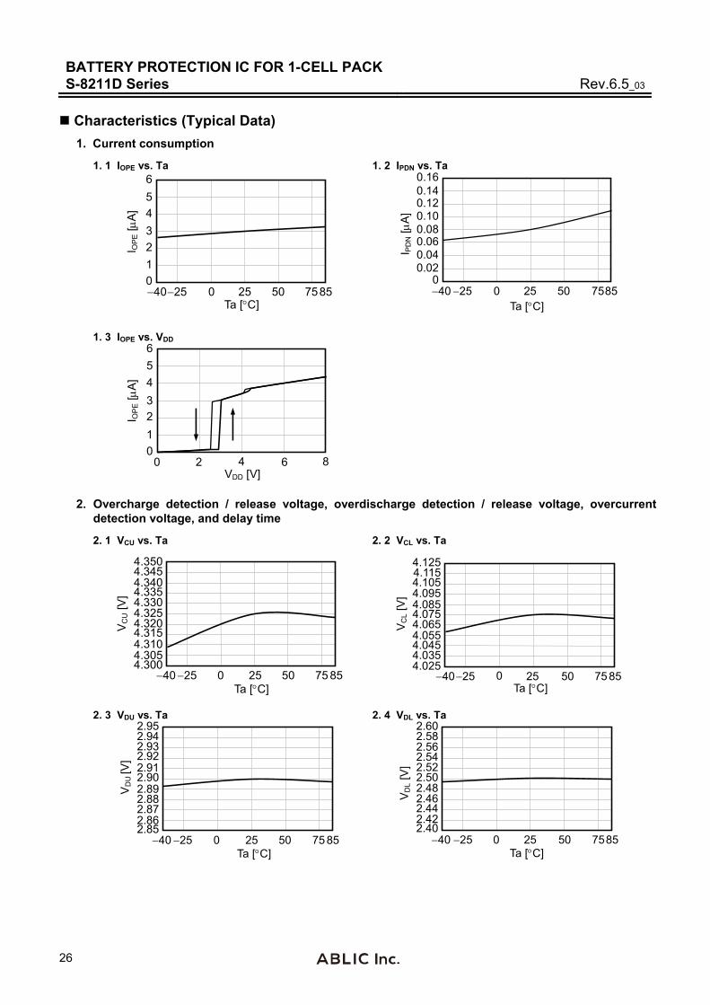
Characteristics (Typical Data)
1. Current consumption
1. 1 IOPE vs. Ta 1. 2 IPDN vs. Ta
40 25 0 25 50 7585
6
5
4
3
2
1
0
Ta [C]
I OP
E [A
]
40 25 0 25 50 7585Ta [C]
0.160.140.120.100.080.06
0
I PD
N [
A]
0.040.02
1. 3 IOPE vs. VDD
0 2 4 6 VDD [V]
6
5
4
3 2
1
0
I OP
E [
A]
8
2. Overcharge detection / release voltage, overdischarge detection / release voltage, overcurrent
detection voltage, and delay time
2. 1 VCU vs. Ta 2. 2 VCL vs. Ta
40 25 0 25 50 75 85Ta [C]
4.350 4.345 4.340 4.335 4.330 4.325
4.300
VC
U [V
]
4.320 4.315 4.310 4.305
4025 0 25 50 75 85Ta [C]
4.1254.1154.1054.0954.0854.075
4.025
VC
L [V
]
4.0654.0554.0454.035
2. 3 VDU vs. Ta 2. 4 VDL vs. Ta
40 25 0 25 50 75 85Ta [C]
2.95 2.94 2.93 2.92 2.91 2.90
2.85
VD
U [V
]
2.89 2.88 2.87 2.86
40 25 0 25 50 7585Ta [C]
2.602.582.562.542.522.50
2.40
VD
L [V
]
2.482.462.442.42

BATTERY PROTECTION IC FOR 1-CELL PACKRev.6.5_03 S-8211D Series
27
2. 5 tCU vs. Ta 2. 6 tDL vs. Ta
40 25 0 25 50 7585Ta [C]
1.50 1.45 1.40 1.35 1.30 1.25
1.00
t CU [s
]
1.20 1.15 1.10 1.05
40 25 0 25 50 7585Ta [C]
200190180170160150
100
t DL
[ms]
140130120110
2. 7 VDIOV vs. Ta 2. 8 tDIOV vs. VDD
40 25 0 25 50 7585Ta [C]
0.175 0.170 0.165 0.160 0.155 0.150
0.125
VD
IOV [
V]
0.145 0.140 0.135 0.130
3.0 3.5 4.0 4.5VDD [V]
14131211109
4
t DIO
V [m
s]
8765
2. 9 tDIOV vs. Ta 2. 10 VSHORT vs. Ta
40 25 0 25 50 7585Ta [C]
14 13 12 11 10 9
4
t DIO
V [m
s]
8 7 6 5
0.750.700.650.600.550.50
0.25
VS
HO
RT [V
]
0.450.400.350.30
4025 0 25 50 7585Ta [C]
2. 11 tSHORT vs. VDD 2. 12 tSHORT vs. Ta
3.0 3.5 4.0 4.5VDD [V]
0.65 0.63 0.61 0.59 0.57 0.55
0.45
t SH
OR
T [
ms]
0.53 0.51 0.49 0.47
4025 0 25 50 7585Ta [C]
1.00.90.80.70.60.5
0
t SH
OR
T [
ms]
0.40.30.20.1

BATTERY PROTECTION IC FOR 1-CELL PACK S-8211D Series Rev.6.5_03
28
3. CO pin / DO pin
3. 1 ICOH vs. VCO 3. 2 ICOL vs. VCO 0
0.1
0.2
0.5
I CO
H [m
A]
0.3
0.4
0 1 2 3 4VCO [V]
0.5
0.4
0.3
0
I CO
L [m
A]
0.2
0.1
0 1 2 3 4VCO [V]
3. 3 IDOH vs. VDO 3. 4 IDOL vs. VDO
0 1 2 3 4VDO [V]
0
0.05
0.10
0.15
0.30
I DO
H [
mA
]
0.20
0.25
0 0.5 1.0 1.5VDO [V]
0.20
0.15
0.10
0
I DO
L [m
A]
0.05
BATTERY PROTECTION IC FOR 1-CELL PACKRev.6.5_03 S-8211D Series
29
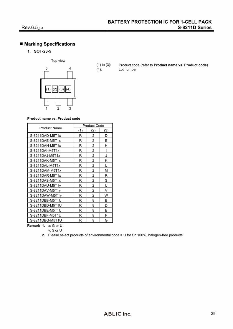
Marking Specifications
1. SOT-23-5
1 2 3
45
Top view
(1) (2) (3) (4)
(1) to (3): Product code (refer to Product name vs. Product code) (4): Lot number
Product name vs. Product code
Product Name Product Code
(1) (2) (3)
S-8211DAD-M5T1x R 2 D
S-8211DAE-M5T1x R 2 E
S-8211DAH-M5T1x R 2 H
S-8211DAI-M5T1x R 2 I
S-8211DAJ-M5T1x R 2 J
S-8211DAK-M5T1x R 2 K
S-8211DAL-M5T1x R 2 L
S-8211DAM-M5T1x R 2 M
S-8211DAR-M5T1x R 2 R
S-8211DAS-M5T1x R 2 S
S-8211DAU-M5T1y R 2 U
S-8211DAV-M5T1y R 2 V
S-8211DAW-M5T1y R 2 W
S-8211DBB-M5T1U R 9 B
S-8211DBD-M5T1U R 9 D
S-8211DBE-M5T1U R 9 E
S-8211DBF-M5T1U R 9 F
S-8211DBG-M5T1U R 9 G
Remark 1. x: G or U y: S or U 2. Please select products of environmental code = U for Sn 100%, halogen-free products.
BATTERY PROTECTION IC FOR 1-CELL PACK S-8211D Series Rev.6.5_03
30
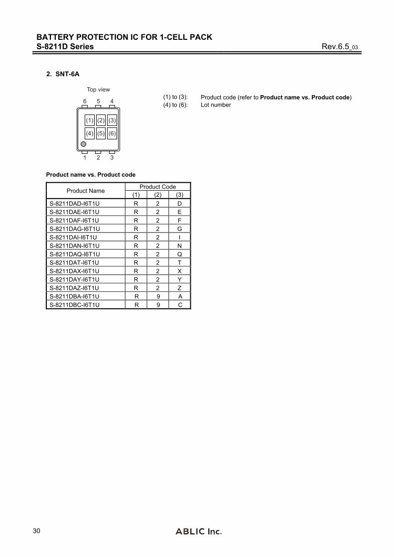
2. SNT-6A
Top view
1 32
6 45
(1) (2) (3)
(4) (5) (6)
(1) to (3): Product code (refer to Product name vs. Product code) (4) to (6): Lot number
Product name vs. Product code
Product Name Product Code
(1) (2) (3)
S-8211DAD-I6T1U R 2 D
S-8211DAE-I6T1U R 2 E
S-8211DAF-I6T1U R 2 F
S-8211DAG-I6T1U R 2 G
S-8211DAI-I6T1U R 2 I
S-8211DAN-I6T1U R 2 N
S-8211DAQ-I6T1U R 2 Q
S-8211DAT-I6T1U R 2 T
S-8211DAX-I6T1U R 2 X
S-8211DAY-I6T1U R 2 Y
S-8211DAZ-I6T1U R 2 Z
S-8211DBA-I6T1U R 9 A
S-8211DBC-I6T1U R 9 C
���
�����
���
����
������ ��
�� ����
�� ����
�� �����
�������
���������������� � �
��
�������������������
���������������
��������������� !"��!"
��

���
�����
���
����
������ ��
#���������
��������
#��������� ������� �������
��������
�������
���
� �
�����������$�������
�������$�������
��������$%&& � & � �%'
( )�)�& *+��!
�������,���'�+*- ".��������/
��

���
�����
���
����
������ ��
�����%0�
������
#������
,��1/ ,��1/
2�3� �4���
�����������5�������
�������5�������
��������5 6
�!6%&7 )�)&%8�!7��!�+- �* !+&%6�'%&+
��

���
�����
���
����
������ ��
��
��������������������
��������� �����
������������� �����
��������
���������
��������������
���
��� ����!
� � !
���
���
�����
���
����
������ ��
"��#�#�$�%&���
���������������
�������
'�������
���
'������������ ���������
���������
��
�������(� �����
������()$$ ��$ � �)*�
�����������(� �����
����
���
��
�
!
� �

���
�����
���
����
������ ��
�����)+�
,�����!
'�!����
-��./ -��./
0�1�
�����������2� �����
�������2� �����
��3)$4�#�#$)5��4����&6��%��&$)3�*)$&
������2��3
�7����
��

���
�����
���
����
������ ��
��
�������������)�#�2�%�����#)&���
��������� ������������������ �����
��!���
����
��!�
����
�
�
��� ��� ������� ������������������ ������������������� ���������� ����������������� ���������
������ ����������� ��������������� ���� ���������� ���������� ����������������� ��!!"���
�������������� ���������� ����������
"�#� �� ������������ ������$���������� �������� ������ �� ���������� ���
%�&����� ��'()��*������+���,��-����'������� ����
��� -�������������@���!�����&<*�/��� �-��!�����A��������/
!!"���
()�
����)<�)&&��&����&��&6��3)�#�*)&&�$��5�#&6�-�������������@���!�����&<*�/���������&�5�#���&6��3)�#�*)&&�$��&��&6��%��&�$��:�&6��*)%?)4���-���!�����A���������/�
��
��� -��!�����A��������/
-�������������@���!�����&<*�/
Disclaimers (Handling Precautions)
1. All the information described herein (product data, specifications, figures, tables, programs, algorithms and application circuit examples, etc.) is current as of publishing date of this document and is subject to change without notice.
2. The circuit examples and the usages described herein are for reference only, and do not guarantee the success of any specific mass-production design. ABLIC Inc. is not responsible for damages caused by the reasons other than the products described herein (hereinafter "the products") or infringement of third-party intellectual property right and any other right due to the use of the information described herein.
3. ABLIC Inc. is not responsible for damages caused by the incorrect information described herein.
4. Be careful to use the products within their specified ranges. Pay special attention to the absolute maximum ratings, operation voltage range and electrical characteristics, etc. ABLIC Inc. is not responsible for damages caused by failures and / or accidents, etc. that occur due to the use of the products outside their specified ranges.
5. When using the products, confirm their applications, and the laws and regulations of the region or country where they are used and verify suitability, safety and other factors for the intended use.
6. When exporting the products, comply with the Foreign Exchange and Foreign Trade Act and all other export-related laws, and follow the required procedures.
7. The products must not be used or provided (exported) for the purposes of the development of weapons of mass destruction or military use. ABLIC Inc. is not responsible for any provision (export) to those whose purpose is to develop, manufacture, use or store nuclear, biological or chemical weapons, missiles, or other military use.
8. The products are not designed to be used as part of any device or equipment that may affect the human body, human life, or assets (such as medical equipment, disaster prevention systems, security systems, combustion control systems, infrastructure control systems, vehicle equipment, traffic systems, in-vehicle equipment, aviation equipment, aerospace equipment, and nuclear-related equipment), excluding when specified for in-vehicle use or other uses. Do not apply the products to the above listed devices and equipments without prior written permission by ABLIC Inc. Especially, the products cannot be used for life support devices, devices implanted in the human body and devices that directly affect human life, etc. Prior consultation with our sales office is required when considering the above uses. ABLIC Inc. is not responsible for damages caused by unauthorized or unspecified use of our products.
9. Semiconductor products may fail or malfunction with some probability. The user of the products should therefore take responsibility to give thorough consideration to safety design including redundancy, fire spread prevention measures, and malfunction prevention to prevent accidents causing injury or death, fires and social damage, etc. that may ensue from the products' failure or malfunction. The entire system must be sufficiently evaluated and applied on customer's own responsibility.
10. The products are not designed to be radiation-proof. The necessary radiation measures should be taken in the product design by the customer depending on the intended use.
11. The products do not affect human health under normal use. However, they contain chemical substances and heavy metals and should therefore not be put in the mouth. The fracture surfaces of wafers and chips may be sharp. Be careful when handling these with the bare hands to prevent injuries, etc.
12. When disposing of the products, comply with the laws and ordinances of the country or region where they are used.
13. The information described herein contains copyright information and know-how of ABLIC Inc. The information described herein does not convey any license under any intellectual property rights or any other rights belonging to ABLIC Inc. or a third party. Reproduction or copying of the information from this document or any part of this document described herein for the purpose of disclosing it to a third-party without the express permission of ABLIC Inc. is strictly prohibited.
14. For more details on the information described herein, contact our sales office.
2.0-2018.01
www.ablicinc.com