Embed Size (px)
Citation preview

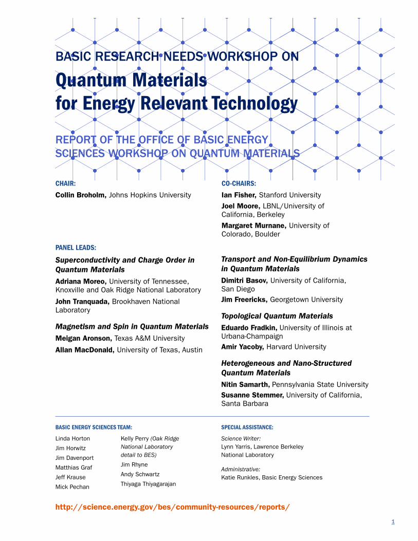
BASIC RESEARCH NEEDS WORKSHOP ON
Quantum Materials for Energy Relevant Technology

2
Cover image: This is an experimental image of the charge density wave of electrons confined to a small quantum dot in a sheet of graphene. The spatial confinement of electrons is being studied as a means of altering the physical properties of graphene and other quantum materials to better understand their behavior and to meet specific application needs. (Image courtesy of Michael Crommie, Lawrence Berkeley National Laboratory).
1
REPORT OF THE OFFICE OF BASIC ENERGY SCIENCES WORKSHOP ON QUANTUM MATERIALS
BASIC RESEARCH NEEDS WORKSHOP ON
Quantum Materials for Energy Relevant Technology
http://science.energy.gov/bes/community-resources/reports/
CHAIR:
Collin Broholm, Johns Hopkins University
CO-CHAIRS:
Ian Fisher, Stanford University
Joel Moore, LBNL/University of California, Berkeley
Margaret Murnane, University of Colorado, Boulder
BASIC ENERGY SCIENCES TEAM:
Linda Horton
Jim Horwitz
Jim Davenport
Matthias Graf
Jeff Krause
Mick Pechan
Kelly Perry (Oak Ridge National Laboratory detail to BES)
Jim Rhyne
Andy Schwartz
Thiyaga Thiyagarajan
PANEL LEADS:
Superconductivity and Charge Order in Quantum MaterialsAdriana Moreo, University of Tennessee, Knoxville and Oak Ridge National Laboratory
John Tranquada, Brookhaven National Laboratory
Magnetism and Spin in Quantum Materials
Meigan Aronson, Texas A&M University
Allan MacDonald, University of Texas, Austin
Transport and Non-Equilibrium Dynamics in Quantum Materials Dimitri Basov, University of California, San DiegoJim Freericks, Georgetown University
Topological Quantum Materials Eduardo Fradkin, University of Illinois at Urbana-ChampaignAmir Yacoby, Harvard University
Heterogeneous and Nano-Structured Quantum MaterialsNitin Samarth, Pennsylvania State UniversitySusanne Stemmer, University of California, Santa Barbara
SPECIAL ASSISTANCE:
Science Writer: Lynn Yarris, Lawrence Berkeley National Laboratory
Administrative: Katie Runkles, Basic Energy Sciences

2
Table of Contents
Executive Summary 4
1 Introduction 6
2 Priority Research Directions in Quantum Materials 11
2.1 PRD 1 — Control and Exploit Electronic Interactions and Quantum Fluctuations for Design of Bulk Materials with Novel Functionality 12
2.1.1 Introduction 12
2.1.2 Scientific Challenges 13
2.1.3 Research Thrusts 16
Thrust 1a: Understand and Control Competing, Coexisting, and Intertwined Order 16
Thrust 1b: Predict, Realize, and Probe New States of Quantum Magnets 23
2.2 PRD 2 — Harness Topological States for Groundbreaking Surface Properties 30
2.2.1 Introduction 30
2.2.2 Scientific Challenges 31
2.2.3 Research Thrusts 31
Thrust 2a: Discover New Topological Quantum Materials 32
Thrust 2b: Design New Platforms to Probe and Exploit Topology 36
2.3 PRD 3 — Drive and Manipulate Quantum Effects (Coherence, Entanglement) in Nanostructures for Transformative Technologies 41
2.3.1 Introduction 41
2.3.2 Scientific Challenges 42
2.3.3 Research Thrusts 43
Thrust 3a: Employ Nanoscale Structuring to Elucidate and Exploit Coherence and Entanglement 44
Thrust 3b: Understand Transport in Quantum Materials 49
Thrust 3c Dynamically Visualize and Manipulate Quantum Materials 58
2.4 PRD 4 — Design Revolutionary Tools to Accelerate Discovery and Technological Deployment of Quantum Materials 65
2.4.1 Introduction 65
2.4.2 Scientific Challenges 67 2.4.3 Research Thrusts 68
Thrust 4a: Enhanced Synthesis of Quantum Materials 68
Thrust 4b: Develop New Windows into Quantum Materials 74
Thrust 4c: Develop Efficient Methods for Static and Dynamic States Beyond 1-Electron Paradigms 79

3
3 Basic Research in Quantum Materials for Energy Relevant Technology 85
3.1 Superconductivity and Charge Order in Quantum Materials 86
3.1.1 Current Status and Recent Advances 86
3.1.2 Scientific Challenges and Opportunities 90
3.1.3 Potential for Energy-Relevant Technologies 94
3.2 Magnetism in Quantum Materials 95
3.2.1 Current Status and Recent Advances 95
3.2.2 Scientific Challenges and Opportunities 99
3.2.3 Potential for Energy-Relevant Technologies 102
3.3 Transport and Non Equilibrium Dynamics in Quantum Materials 104
3.3.1 Current Status and Recent Advances 104
3.3.2 Scientific Challenges and Opportunities 105
3.3.3 Potential for Energy-Relevant Technologies 109
3.4 Topological Quantum Materials 110
3.4.1 Current Status and Recent Advances 112
3.4.2 Potential for Energy-Relevant Technologies 114
3.5 Heterogeneous and Nano-Structured Quantum Materials 117
3.5.1 Current Status and Recent Advances 117
3.5.2 Scientific Challenges and Opportunities 118
3.6 Cross-Cutting Themes 121
3.6.1 Materials Synthesis 121
3.6.2 Instrumentation 128
3.6.3 Theory and Modeling 133
Appendix A: Workshop Participants 135
Appendix B: Workshop Agenda 141
Appendix C: Abstracts for Plenary Talks 143
References 146
Figure Sources 164
4
Executive Summary
Just as the discovery of semiconductors revolutionized computation and information storage, and ushered in today’s hundred-billion dollar electronics industry, quantum materials have the potential to revolutionize energy and energy-related technologies, as well as the storage and processing of data, with possible economic ramifications of staggering proportions. Even now new quantum materials are emerging that feature unprecedented capabilities. One quantum material just entering the public radar is graphene — a sheet of carbon just one atom thick. Not only is graphene 200 times stronger than steel while weighing less than paper, but electrons race through its two- dimensional plane 100 times faster than they move through silicon. While graphene has already been identified as a potential superstar by the electronics industry, new quantum materials are emerging to challenge it. For example, two-dimensional (2D) transition metal dichalcogenides (TMDCs) are more device-ready than graphene and offer other advantages for high-speed, low-power electronics. Additional breakthroughs are being seen in materials known as “topological insulators” where novel properties are found in electronic states that only exist on the material’s sur-face. From TMDCs and topological insulators to materials that display other extraordinary effects such as “quantum spin liquids” and high-temperature superconductivity, we see the dawn of a new era of quantum materials.
To realize the tantalizing potential of quantum materials, there is much basic scientific research to be done. Recognizing the high potential impact of quantum materials, nations around the world are already investing in this effort. We must learn how the astonishing properties of quantum materials can be tailored to address our most pressing technological needs, and we must dramatically improve our ability to synthesize, characterize, and control quantum materials. To accelerate the progress of quantum materials research, the U.S. Department of Energy’s Office of Science, Office of Basic Energy Sciences (BES), sponsored a “Basic Research Needs Workshop on Quantum Materials for Energy-relevant Technology,” which was held near Washington, D.C. on February 8–10, 2016. Attended by more than 100 leading national and international scientific experts in the synthesis, characterization, and theory of quantum materials, the workshop identified four priority research directions (PRDs) that will lay the foundation to better understand quantum materials and harness their rich technological potential.
Imagine future computers that can perform calculations a million times faster than today’s most powerful
supercomputers at only a tiny fraction of the energy cost. Imagine power being generated, stored, and then
transported across the national grid with nearly no loss. Imagine ultrasensitive sensors that keep us in the loop
on what is happening at home or work, warn us when something is going wrong around us, keep us safe from
pathogens, and provide unprecedented control of manufacturing and chemical processes. And imagine smart
windows, smart clothes, smart buildings, supersmart personal electronics, and many other items — all made
from materials that can change their properties “on demand” to carry out the functions we want. The key to
attaining these technological possibilities in the 21st century is a new class of materials largely unknown to
the general public at this time but destined to become as familiar as silicon. Welcome to the world of quantum
materials — materials in which the extraordinary effects of quantum mechanics give rise to exotic and often
incredible properties.

5
Priority Research Directions
Control and exploit electronic interactions and quantum fluctuations for design of bulk materials with novel functionality
One of the effects of quantum mechanics is spontaneous “quantum fluctuations” of physical quantities that can break down conventional order in solids and usher in entirely new forms of electronic order. The resulting material properties, coupled to an extreme sensitivity to external perturbations, hold promise for novel functionality that could impact technologies ranging from power management and transmission, to platforms for quantum computation, to novel versatile sensors.
Harness topological states for groundbreaking surface properties
Topological materials are a newly discovered class of quantum materials with distinct electronic properties in a protected surface region. As in graphene, the 2D electronic nature of topological materials offers potentially game-changing advances in the energy and electronics industries because they support switchable electrical currents on their surfaces with dramatically lower energy loss.
Drive and manipulate quantum effects (coherence, entanglement) in nanostructures for transformative technologies
Nano-structured quantum materials can be externally manipulated beyond thermal equilibrium using new techniques for ultra-fast, coherent excitation. The formation of quasiparticles with exotic names such as skyrmions, magnons, and spinons, and the seemingly magical qualities of quantum effects such as coherence and entanglement in these materials offer a pathway to ultra-fast, ultra-energy efficient computing with seamless linkages to optical communications.
Design revolutionary tools to accelerate discovery and technological deployment of quantum materials
The development of new methodologies and tools will accelerate the discovery of new quantum materials and advance the ability to probe, predict, and exploit their remarkable properties.
Detailed discussions of the four PRDs along with guidelines and recommendations for achieving their objectives are provided in Chapter 2 of this report. Chapter 3 includes the detailed background information on quantum materials developed as part of the workshop. The full report can be accessed on-line through the BES website.
Quantum materials are solids with exotic physical properties, arising from the quantum mechanical properties of their constituent electrons; such materials have great scientific and/or technological potential.

6
1 Introduction
“He who sees things grow from the beginning will have the best view of them...” — Aristotle
Every day of your life, you encounter thousands of distinct materials. The text you are now reading is made either from ink on a paper substrate or pixels on a computer display. The clothes on your back, the containers that hold your food and beverages, the buildings that give you shelter, the vehicles that transport you, the energy systems that power them and the roads they travel, the tools with which you work, and the devices that inform or entertain you — all reflect the ubiquity of engineered materials in modern life.
At an accelerating pace stretching from the pre-historic age of stone tools to the age of bronze alloys, to the transfor-mation of iron into steel, to zone-refined silicon for electronics, the progression of human society is inextricably linked to its ability to make and use materials. As we continue to manipulate materials to satisfy our needs, it is inevitable that we should eventually reach the atomic scale. There, as matter aquires wavelike properties, we find quantum phenomena such as interference, tunneling, fluctuations, entanglement, and topological effects that are perhaps even more counterintuitive and surprising to us than the strength of bronze to our ancestors. The quest to understand such intriguing phenomena stimulates progress in fundamental and applied science that often leads to profound and unexpected benefits for both. Based on the rapid advancement in our understanding and control of interacting elec-trons at the atomic scale, “quantum materials” are poised to transform an array of critical technologies, particularly those related to information and energy.
Before the advent of quantum mechanics, magnetic materials seemed so magical that Thales of Miletus in the sixth century BC ascribed a soul to lodestone (Fe3O4) because “it causes movement to iron”[1]. In the ensuing millen-nia, inventive navigators took advantage of lodestone in compasses, although a proper understanding of how the electrons in a solid become magnetized had to wait until the 20th century. The strongly quantum-mechanical nature of electrons in many solids leads to them being called quantum materials. Leaps in our understanding of quantum materials are now positioned to enable technologies as revolutionary as the compass was in its day.
Solid-state magnetism is based on the spin and orbit of the electron, which also underlie new approaches to comput-ing. Spin is the intrinsic rotational momentum of a quantum particle — here an electron, which is quantized to spin up or down (corresponding to two senses of rotation). A modern hard disk is based on magnetic regions that are tiny, with more than a trillion bits per square inch, but each region still includes nearly a million spins. Improving our con-trol of magnetism at the single-spin level and finding new types of magnetic ordering in quantum materials will enable improved computer memory and logic devices to extend the information technology revolution.
Quantum materials may enable fundamentally new approaches to computation, such as quantum or neuromorphic computing, to progress from fantasy to reality. Advances in our understanding of quantum materials could enable the construction of neuromorphic computers that mimic the human brain by learning and adapting as they interact with the world. Quantum computing has the potential to render trivial certain critical mathematical tasks that are now practically impossible to solve even on the world’s fastest supercomputers. The blinding speed and awesome power
7
of quantum computing could be made possible by the weird but demonstrably real effects of quantum mechanics. Today’s information technologies largely rely on the electrical charge of electrons to store and process individual “bits” of information as either a one or a zero. Under quantum computing, information would be processed and stored in “qubits” that behave as both a one and a zero at once to enable massively parallel computation.
Even current “classical” computing is in a position to be revitalized by the development of quantum materials. The portable electronic devices upon which we so heavily depend in our daily lives (cell phones, tablets, laptops, and the associated cloud infrastructure) now consume a substantial and rapidly growing amount of energy (estimated at 5% of the world’s total electricity generation in 2012 and growing faster than other sectors [2]). Quantum materials, with their potential for enabling smaller and far more energy-efficient Information and Communication Technology (ICT) devices, can reduce energy use while increasing performance.
One of the most dramatic phenomena in quantum materials is superconductivity — the ability of a material to sup-port electrical current flow with zero resistance, meaning no energy is lost to heating or other inefficiencies, through the interaction of its electrons. Superconductivity was first observed in simple metals and typically occurs in such materials only near the absolute zero temperature (–273° Celsius). The most powerful and compact magnets in the world, used to channel high-energy particles in colliders or to diagnose disease through magnetic resonance imaging (MRI), are based on superconducting materials, because a superconductor can carry enormous electrical current densities that would otherwise melt even a good conductor like copper. However, the extraordinarily cold temperature requirements for conventional superconductors severely limit their technological application.
In the late 1980s, scientists learned that some quantum materials are superconducting at higher temperatures (above the boiling point of liquid nitrogen, so cooling them is relatively simple). These “high-temperature supercon-ductors” are now being used as power cables to efficiently bring electrical power to high-rise buildings in Seoul. At the demonstration level, superconductors have also been used to “levitate” a train (hold the train above the tracks to reduce friction losses) and propel it at 375 mph in Japan (non-superconducting maglev technology is already commer-cially operating in Shanghai, Japan, and South Korea.). For the generation of energy through fusion reactions, super-conductors are being used to create magnetic “bottles” that confine the fusing plasma, which is so hot no material in physical contact with the plasma could contain it. More widespread application of superconductivity has the potential to save tens of billions of dollars in energy transmission, generation, and storage losses. By enhancing the correla-tions between electrons so superconductivity can be sustained at even higher temperatures, quantum materials could transform our energy distribution systems, the medical and scientific applications of strong magnetic fields, and potentially all transportation and energy production sectors.
While ferromagnetism has been known to humankind for more than 2,500 years and superconductivity was first observed a century ago, other classes of quantum materials were discovered much more recently. Topological insulators are an example from the last decade: these are materials that are insulating in the bulk, while the surface supports an atomically thin conducting layer. As artificially created thin conductors are the basis of special transis-tors used in cell phones and other applications, materials that spontaneously support surface conduction are quite appealing. Two other directions with great progress in recent years are the manipulation of quantum materials at extremely short time scales (well under a trillionth of a second) and their manipulation in space at the atomic scale.
In recognition of the tremendous scope and scale of the transformative opportunities offered by quantum mate-rials, the U.S. Department of Energy’s Office of Science held an intense three-day workshop on the subject near Washington, D.C. on February 8–10, 2016. The “Basic Research Needs Workshop on Quantum Materials for Energy-relevant Technology” was attended by more than 100 leading national and international scientific experts in the synthesis, measurement, and theory of quantum materials. Attendees were organized into panels that examined the current state of the field in such key areas as superconductivity, quantum magnetism, transport and non-equilibrium dynamics, topological materials, heterostructured quantum materials, and the “tools” needed to synthesize, probe, and model quantum materials. From these panels, four priority research directions (PRDs) were identified, based on the compelling nature of fundamental questions and the potential for future impact on energy-relevant technologies.
8
PRD 1: Control and exploit electronic interactions and quantum fluctuations for design of bulk
materials with novel functionality
Many of the remarkable properties of quantum materials result from strong interactions among their constituent elec-trons and the rich variety of ordered states, including superconductivity, that emerge as a consequence, often in close proximity to each other in a given phase diagram. Associated properties include an extreme sensitivity to perturba-tions, affecting electronic, magnetic, optical, and thermal properties; in some cases quantum entanglement (in which an action on one electron influences another electron, even if the two are separated by a substantial distance and do not directly interact); and in the case of superconductivity. To assess the utility of these materials for applications, and enhance their potential functionality, fundamental research is required to understand the organizing principles that govern electron dynamics in the presence of strong quantum fluctuations. Looking beyond the standard para-digms of simple metals and semiconductors, how are strongly interacting electrons organized in quantum materials, and how can this organization be controlled for energy-relevant technologies? Research thrusts under this PRD specif-ically target a comprehensive understanding of complex phase diagrams, including the interplay of collective modes with quasiparticle dynamics and the discovery and characterization of new electronic phases. For all materials, new means to understand and control the effects of quenched disorder are required. For the specific case of quantum spin liquids, new methods to expose quantum entanglement are also needed. A central, but still poorly understood, concept in all of these areas is that of the quantum phase transition in metals. Significant advances in these areas could lead to improved superconductors for power applications, improved materials for information storage and pro-cessing, and new materials for sensing and quantum computing.
PRD 2: Harness topological states for groundbreaking surface properties
In topological materials, the geometry of the quantum-mechanical “wave function” that describes the material’s elec-trons has a complex structure with some simple and important consequences. For instance, a material’s surface can behave fundamentally differently from the bulk. Topological insulators, for example, are electrically insulating in the bulk but have atomically thin conducting surface layers. The area of topological materials has seen remarkable and unexpected progress in the past decade enabled by close connections between experimental and theoretical work. However, we are far from the understanding and control needed for technological applications.
Much of the scientific excitement and potential utility of topological quantum materials can be traced to two proper-ties. The first is dissipationless electron transport — the ability to support large, switchable electric currents without energy loss. The dissipationless transport of electrons in a topological quantum state is similar to the transport of electrons in a superconductor, in both cases the ground state of the material can transport electrons. So, topological quantum materials present exciting new opportunities for applications of quantum transport. Harnessing topological quantum states offers a new approach to increasing the energy efficiency of current computing and thermoelectric devices, as well as creating new kinds of devices based on spin transport.
The second unique property of topological quantum states is that they can host electron-derived quasiparticles with significantly different properties than the original electrons. Quasiparticles can, for example, carry fractional charges so that it takes several of them to equal the charge of an electron. The result is that, within the confines of the mate-rial, the electron has been fractionalized. In two-dimensional systems, fractionalized quasiparticles can be non-abe-lian, meaning that the physical exchange of two identical particles fundamentally alters the underlying quantum state. Quasiparticles in topological quantum materials offer new approaches to the computing process itself, including the creation of robust quantum computers that are desensitized to noise and disorder. Significant scientific effort, outlined in the report, is needed to improve topological materials so their dissipationless transport and fractional quasiparticles can be the basis for disruptive electronic devices.

9
WHAT IS A QUANTUM MATERIAL?
All materials require quantum mechanics, but not all materials are quantum materials
Any successful theory of a solid, capable of accurately describing its thermodynamic and electronic properties, is necessarily based upon a quantum mechanical treatment of electrons, and excitations of the atomic lattice (phonons). Furthermore, there are many situations where quantum mechanics enters at the nanometer scale and affects even large-scale properties of materials that are otherwise described very satisfactorily using classical models. For example, the ionic motion that is crucial for battery performance is classical on large scales even though quantum effects are essential to understand ionic motion. Even the large-scale mechanical properties of structural steels, including their ductility and crack resistance, are determined by single defects with quantum-mechanical properties. The materials described in this report, however, are defined by more esoteric, but manifestly real, quantum effects, such as quantum fluctuations, quantum entanglement, quantum coherence, and the topology of the quantum mechanical wave functions. Significantly, such “quantum materials” harbor exotic physical effects with great technological potential.
Quantum effects in solids
In general, a sure sign of quantum mechanics is that some properties become quantized to a discrete set of values when a continuous range exists in classical physics. A dramatic example of this is that electrons carry an intrinsic magnetic moment or “spin.” Aside from moving through space, an electron’s magnetic moment along any axis takes exactly two possible values in a measurement. Another property of quantum mechanics, the superposition principle, says that if the electron is not mea-sured then a combination of these two spin states is allowed. Both the discreteness of spin and the superposition principle are essential for explaining why some solids are magnetic. Quantum mechanics also imbues a wavelike nature to particles, including electrons. Electrons flow through an ordinary metal when an electric field is applied. Viewing electrons as forming a “classical” (non-quantum mechanical) fluid is not a bad starting point but is not strictly correct and leads to grossly wrong numerical values for some quantities. When one or two dimensions of the metal are shrunk, however, electronic motion becomes strongly modified by the wavelike nature of the electron, producing a quantum well or quantum wire. This can lead to dramatic properties, such as quantized conductance, that have no classical analogue.
The zoo of quantum materials
The number of combinations of elements that can be imagined in solid materials is enormous, and the resulting zoo of materials can seem daunting. Scientists, however, simplify this by classifying materials according to broad categories that define or describe the general types of electronic behavior in these materials. Three examples of the types of electronic behavior, and the impact that such materials might have on the energy landscape, are outlined below. Others are described throughout the report.
In topological materials the quantum mechanical wave functions of electrons have non-trivial geometry that “protects” coherent wavelike electronic transport at all surfaces and could form the basis for a new generation of energy-efficient electronics.
In superconductors electrons form a collec-tive wave that permeates the material. The underlying electronic wave coherence in these materials leads to the complete loss of electrical resistance and expulsion of magnetic fields so that a ferromagnetic material (cube in the figure) levitates above superconductors. A practical high-tem-perature superconducting material could transform energy production, storage, trans-mission, and utilization.
In quantum spin liquids the spins of the constituent electrons become entangled and fail to form a static ordered state as in a conventional magnet. Energetic defects in this quantum fluctuating state, called “quasi-particles,” supplant the individual electrons as the “moving parts” of the solid and could become the basis for revolutionary information storage and processing.

10
PRD 3: Drive and manipulate quantum effects (coherence, entanglement) in nanostructures for
transformative technologies
Today’s silicon-based information technologies are approaching physical limits set by dissipation, density, and speed. Quantum materials, by comparison, offer a staggering array of new electronic functionalities that promise to extend and expand current information technologies far beyond the capabilities of silicon. The potential technological bounty of quantum materials stems from the exotic quasiparticles they can harbor (magnons, spinons, visons, skyrmions, magnetic monopoles, phonons, etc.) which, within the material, are as real as the electrons and photons that drive the Internet. These quasiparticles boast quantum behaviors — coherence, entanglement, and quantum transport — the exploration of which in nano-structured quantum materials provides abundant opportunities for fundamental discoveries that enable radical new low-power information storage and processing. This PRD focuses on the explo-ration of the transport and non-equilibrium properties of quantum materials and the heterogeneous and finite-sized structures that reveal fundamental properties, which can be the basis for transformative technologies. Stimulating quantum materials with femtosecond light pulses can, for example, create metastable states of matter with specific electronic functionalities that do not exist in equilibrium. Desirable properties, such as superconductivity, may be enhanced by exciting specific vibrational states (phonons), and magnetic bits in nanostructures may be individually switched with spatially patterned optical driving fields. The rich interactions between light and quantum materials offer outstanding opportunities to transfer information from fiber-optical encoding to quasiparticle assemblies for infor-mation processing within a quantum material. Nano-structured quantum materials thus open the possibility of a new class of ultra-fast and energy-efficient electronics with seamless linkages to optical communication systems.
PRD 4: Design revolutionary tools to accelerate discovery and technological deployment of
quantum materials
The remarkable properties of quantum materials that are generating such keen scientific interest — including the ability to alter their electronic state, their magnetic state, and their structure through external stimuli, and to transport spin and charge with extreme efficiency — also pose immense challenges to the experimental and theoretical work required to understand and exploit them. This PRD calls for the development of the necessary tools to address these challenges, affecting the synthesis, characterization, and theoretical treatment of quantum materials. Key challenges include establishing appropriate methods to grow and manipulate complex and nano-structured quantum materials with desired purity and controlled levels of dopants and defects. Research opportunities encompass (1) development of new in situ and in operando characterization and feedback techniques to discover materials with improved proper-ties and functionalities; (2) characterization and control of quantum material properties on all length and time scales relevant to function, including tools to reveal the often subtle forms of emergent and topological order; and (3) predic-tion of the fundamental properties of quantum materials, including emergent order, behavior far from equilibrium, and functionality in the presence of disorder. Progress in these areas will enable the science described in the other PRDs. These new capabilities will also have a broad impact across wide ranges of materials with potential applications in energy and computational sciences, nanotechnology, nano-manufacturing, and nano-engineering.
Achieving the objectives presented in this report have potential rewards in terms of strengthening our nation’s economy and energy security that are as stunning as the properties of quantum materials themselves. Research into quantum materials has become a worldwide enterprise amongst all of the technologically advanced nations because there are billions of dollars to be realized in the next generation of information and energy-relevant technologies.

11
2. Priority Research Directions in Quantum Materials
The workshop discussions identified four Priority Research Directions (PRDs) that define the basic research
needed to develop energy-relevant technologies based on quantum materials. Each PRD is discussed in depth
with the associated research thrusts in this chapter. As background, Chapter 3 of the report provides an in-depth
assessment of the current status of research in the field of quantum materials.
Table 1: List of Priority Research Directions and Associated Research Thrusts
1. Control and exploit electronic interactions and quantum fluctuations for design of bulkmaterials with novel functionality Looking beyond the standard paradigms of simple metals and semiconductors, how do strongly-interacting electrons organize themselves in quantum materials, and how can this be controlled for energy-relevant technologies?
Thrust 1a: Understand and control competing, coexisting, and intertwined order
Thrust 1b: Predict, realize, and probe new states of quantum magnets
2. Harness topological states for groundbreaking surface propertiesBuilding on recent advances in the field of topological insulators, what new topological states of matter can be realized, what are their signatures, and how can these be used for energy-related applications?
Thrust 2a: Discover new topological quantum materials
Thrust 2b: Design new platforms to probe and exploit topology
3. Drive and manipulate quantum effects (coherence, entanglement) in nanostructures fortransformative technologiesHow can the extraordinary properties of coherent quantum states be controlled and utilized for energy- related applications?
Thrust 3a: Employ nanoscale structuring to elucidate and exploit coherence and entanglement
Thrust 3b: Understand transport in quantum materials
Thrust 3c: Dynamically visualize and manipulate quantum materials
4. Design revolutionary tools to accelerate discovery and technological deployment ofquantum materialsWhat new methodologies and tools are needed to advance synthesis of quantum materials and our abilityto probe and predict their properties?
Thrust 4a: Enhanced synthesis of quantum materials
Thrust 4b: Develop new windows into quantum materials
Thrust 4c: Develop efficient methods for static and dynamic states beyond 1-electron paradigms
12
2.1 PRD 1 — CONTROL AND EXPLOIT ELECTRONIC INTER-ACTIONS AND QUANTUM FLUCTUATIONS FOR DESIGN OF BULK MATERIALS WITH NOVEL FUNCTIONALITY
Quantum materials present a range of remarkable properties with enormous potential for future energy-relevant
technologies. To assess the utility of these materials for applications, and enhance their potential functionality,
fundamental research is required to understand the organizing principles that govern electron dynamics in the
presence of strong quantum fluctuations. Looking beyond the standard paradigms of simple metals and semicon-
ductors, how are strongly interacting electrons organized in quantum materials, and how can this organization be
controlled for energy-relevant technologies? Research directions specifically seek a comprehensive understand-
ing of complex phase diagrams, including the interplay of collective modes with quasiparticle dynamics and the
discovery/characterization of new electronic phases. This will require the development of new methods to expose
quantum entanglement as well as the means to understand and control the effects of quenched disorder. A cen-
tral, but still poorly understood, concept in all of these areas is that of the quantum phase transition in metals.
Significant advances in these areas could lead to improved superconductors for power applications, improved
materials for information storage and processing, and new materials for quantum computing.
2.1.1 Introduction
The central thesis of this PRD is that fundamental research aimed at understanding the basic organizing principles that are at play in quantum materials is required to assess their utility for energy-relevant technologies, and where possible to enhance appropriate functionality. Why do the constituent electrons arrange themselves in the ways that they do, and how can this be controlled? Three particular characteristics that quantum materials can exhibit, which are particularly promising from the perspective of potential energy applications and yet are incom-pletely understood, are their large responses to external perturbations, quantum entanglement, and (sometimes unconventional) superconductivity.
Large responses to external perturbations: Many quantum materials are characterized by extreme sensitivity to small perturbations. This behavior is due in part to the nature of the electronic phase transitions that often occur in these materials (for example, metal-insulator transitions driven by electron correlation) and because many quantum materials are characterized by multiple proximate electronic phases. The relative stability of these phases can be tuned by subtle variations of a variety of parameters. Another factor influencing the behavior is the coupling of elec-trons to intense quantum fluctuations that occur when ordered states are suppressed, leading to unresolved com-petition among alternative forms of order. Proximity to these nascent phase transitions can lead to extremely large changes in physical properties such as the conductivity, optical reflectivity, dielectric constant, and magnetic sus-ceptibility. Such large responses to small perturbations could be utilized as the key component of sensitive detec-tors, as the active component in high-power electronic switches, or as electronically activated optical components. Similarly, some quantum materials exhibit multiferroic behavior due to strong coupling among the charge, orbital, and magnetic responses of the electrons and, for example, provide avenues to control the magnetic response of a material by electric fields and vice versa. When fluctuations and interactions are sufficiently strong, the itinerant nature of the electrons can be greatly reduced and even completely suppressed, and this incipient electronic local-ization can greatly affect the transport of heat and electricity, which is of potential interest for new families of hybrid

13
devices for the conversion and management of heat. Progress towards incorporating any of these effects into future technologies rests on obtaining a fundamental understanding of the factors governing the complex phase diagrams and phase transitions found in quantum materials.
Magnetic degrees of freedom and quantum entanglement: As ever-increasing amounts of energy are consumed in computation and information storage, it is highly desirable to replace conventional transistors and logic elements with new devices that consume less power. Exotic magnetic systems could play a key role in low-power computation because their magnetic moments can be manipulated without incurring energy costs due to charging. This is already a factor in the rise of spintronics based on conventional magnetic materials, and further improvements may be envisaged by the use of exotic magnetic systems (for example those where spinons carry information). In addition, novel quantum spin liquid phases are predicted to have strongly entangled quantum states, which could be used as components in future quantum computers. More generally, the discovery and characterization of exotic magnetic states of matter have demonstrated that protection against various forms of disorder is possible. These insights could potentially be useful for information processing in the future. A central goal of this PRD is to predict and realize new materials that exhibit these sorts of exotic properties, and where magnetism is governed by quantum entanglement rather than symmetry breaking.
Superconductivity: Many quantum materials exhibit unconventional superconductivity in their phase diagrams. These superconductors can have some remarkable properties, including high critical temperatures (the temperature below which the material is superconducting). The ability of a superconducting wire to carry a current without loss has numerous significant applications directly relevant to energy. In fact, there are already areas where supercon-ductors are used because their performance exceeds that of conventional conductors. Examples include the use of superconducting coils to generate the high magnetic fields needed for MRI, superconducting coatings in radio- frequency cavities for advanced particle accelerators, and use in maglev trains where superconducting properties allow the train to be levitated above the track to reduce energy consumption and enhance the speed.
There is also potential for improved superconductors to impact the electrical power grid (see the sidebar “Energizing and Protecting the Grid”). Superconducting cables carry more power in a smaller cross section than conventional cables, a distinct advantage in congested cities where replacement cables must fit within restricted space. Also, superconducting fault current limiters introduced into the grid can prevent anomalous power swings from causing blackouts, such as the major event that struck the northeastern U.S. in 2003. Moreover, electrical generators made from superconducting wires will enable powerful offshore wind turbines that can operate without the need for frequent maintenance. Furthermore, the impact on the grid from cycles in the demand for electricity and intermittent energy generation could be mitigated with superconducting magnetic energy storage devices that can rapidly absorb and release energy, thus providing a stabilizing factor.
These grid applications are already within reach; the challenge is to make them cost-effective. This can be accom-plished in several ways. One is to improve the performance of existing superconducting wires, while limiting production costs. Another approach is to discover new superconductors, with good vortex-pinning properties, that operate at higher temperatures, thus reducing the cooling costs. This PRD focuses on understanding the many factors that come together to determine the critical temperature and other physical properties of unconventional superconductors.
2.1.2 Scientific Challenges
Organizing principles in quantum materials: At very low temperatures, helium is the canonical example of a “quan-tum liquid”; strong quantum fluctuations melt (destroy) long-range atomic order, and the resulting liquid must be evaluated using appropriate quantum statistics rather than the classical approaches appropriate for liquids such as water. The resulting superfluid states of liquid He-3 and He-4, which exhibit zero viscosity and several other remark-able properties, demonstrate the astonishing macroscopic properties that can arise from quantum mechanics.
14
In contrast to liquid helium, solid quantum materials maintain an ordered atomic lattice, and quantum fluctuations are primarily associated with their electronic and magnetic degrees of freedom. By analogy to quantum liquids, one might anticipate similarly remarkable emergent collective electronic properties in such materials; this turns out to be the case, but the situation is much more complex than for liquid helium, and there is not yet a comprehensive understanding of the organizing principles.
The melting of long-range order by quantum fluctuations results in a quantum phase transition. For metallic systems, this is particularly complex due to the interaction of ungapped electronic states with the fluctuating order. Materials tuned to such a state can exhibit a variety of poorly understood effects which can persist at much higher tempera-tures than the superfluid states of liquid helium, including strange metal behavior, new types of emergent order, unconventional superconductivity, and often an extreme sensitivity to perturbations and disorder. These emergent electronic behaviors can develop from the interaction of the electrons among themselves via Coulomb repulsion or with other degrees of freedom present in the quantum materials such as spins, phonons, or orbitals.
Order does not necessarily only arise from broken symmetries, but also from the stabilization of topological phases, characterized by discrete values of topologically invariant quantities. Of these, quantum spin liquids potentially provide access to highly entangled quantum states, and, if metallized, might also provide a pathway to high-temperature superconductivity.
All of these remarkable properties of quantum materials have the potential for use in energy-relevant technologies, but making use of quantum materials requires fundamental research to understand the relevant organizing princi-ples and control the resulting behavior.
Order and disorder: Quantum phase transitions, in which an ordered electronic state is melted by appropriate tuning of a non-thermal variable, were originally conceived in the context of the suppression of a single homoge-neous phase. More recently, though, it has become evident that other, more complex, behaviors can often manifest. Understanding these more complex behaviors is a central priority for future research in quantum materials, particu-larly for those that might find applications in energy-relevant technologies.
Ordered electronic states might in some circumstances melt via a sequence of phase transitions. An example of such “partial melting” is provided by the nematic liquid crystal phase, which corresponds to a partially melted smectic phase. There is growing evidence for similar behavior in several families of high-temperature superconductors, including possible electronic nematic phases, but the physical origins of these effects in specific materials are not fully understood. Do emergent phases result from competition among the various present degrees of freedom? Or perhaps they are the consequence of a cooperative interaction among the degrees of freedom? What is the role that disorder — a necessary ingredient in the doping usually needed to stabilize the emergent phases — plays in their microscopic structure? Do the fluctuations associated with the partially melted phases have direct or indirect consequences on any emergent order close to an eventual quantum critical point? Could any of these mechanisms be an important factor in determining the critical temperature of high-temperature superconductors? In short, what are the origins, nature, and consequences of the various broken symmetry phases found in such systems? What role do they play in any supercon-ducting pairing interaction, and how can they be controlled to optimize desired electronic properties?
Partially melted order provides a clear example of electronic phases that go beyond the classical example of competing order. Other classes of “intertwined” order have been observed in quantum materials, such as the “CE” phase in the colossal magnetoresistive (CMR) manganites, which are characterized by simultaneous charge, spin, and orbital order. Exotic phases such as pair density wave states have also been proposed in the context of superconducting cuprates. Indeed, recently it has become apparent that the phase diagrams of several quantum materials contain many different, possibly intimately related, types of electronic order, often with comparable critical temperatures. It is unclear to what extent this behavior reflects the possible presence of an underlying quantum critical point, or whether it results from the interaction among the various degrees of freedom combined with effects of disorder. Understanding such complex phase diagrams requires new theoretical perspectives, new experimental

15
probes, and development of well-controlled materials that cleanly exhibit specific types of order characterized by specific broken symmetries.
Many metallic quantum materials exhibit “strange metallic” behavior that is inconsistent with conventional Fermi liquid theory. In many cases, these effects have been loosely associated with quantum criticality, but they could also arise from intrinsic inhomogeneous states, or from states with intertwined orders, none of which are well understood. Abandoning Fermi liquid theory is unsettling but apparently necessary for such materials. What should it be replaced with? How should we explain the thermally excited states of inhomogeneous, quantum mechanically fluctuating metals, and how do these states connect to any eventual emergent order at low temperatures?
It has also become clear that many, perhaps most, materials of current interest for potential technological applica-tions are far from pristine and homogeneous. Originally, such imperfections were seen as hampering elucidation of the key physical properties. However, more recently it appears that, in at least some materials, the disorder may be a vital ingredient. Indeed, there are reasons to think that disorder can have profound effects on materials in a “quantum critical” regime. What if disorder were a key feature affecting the various types of emergent electronic properties of many more quantum materials? Could controlled disorder be used to unleash and control desirable functionalities in quantum materials? Addressing these questions requires both new theoretical and new exper- imental approaches.
Quantum spin liquids — new types of topological order: Certain states of matter resist characterization in terms of broken symmetries associated with a local quantity such as spontaneous magnetization or the superfluid phase. Instead, they are distinguished by global properties known as topological invariants. Whereas conventional phase transitions have a local order parameter present on one side of the transition and absent on the other, topological phase transitions are accompanied by a discontinuous change in a global topological invariant, such as the Chern number of electronic energy bands or the global flux of an emergent gauge field. Elementary excitations in these phases of matter may have fractionalized quantum numbers and may exhibit “anyonic” statistics. Topological materials are part of two PRDs with PRD 1 covering the topology of quantum spin liquids and PRD-2 focusing on topologically protected surface states.
Quantum spin liquids are a new class of topologically ordered states, constituting a new frontier for both theorists and experimentalists. Such systems provide a rich variety of qualitatively new collective states of matter. Ultimately, they may also form the basis for groundbreaking applications, such as in decoherence-resistant quantum computing.
Injecting mobile charge into quantum spin liquids could be one of the most important pathways to realizing new quantum states of matter. The singlet spin pairs that dominate a quantum spin liquid closely resemble Cooper pairs in superconductors. One of the predictions of P. W. Anderson’s Resonating Valence Bond (RVB) theory of high- temperature superconductivity is that when charge is injected into a spin liquid, the pairs from the spin liquid will provide the strong singlet correlations necessary for the formation of a superconducting material [3]. At the very least, it is believed that new kinds of metallic states could emerge from doped spin liquids, with a strong suscepti-bility for new kinds of order, including superconductivity. The discovery of new spin liquids, and their metallization, is key to realizing this potential.
Positive experimental identification of a quantum spin liquid (as opposed to simply not observing any signatures of long-range order) has, thus far, remained elusive. Consequently, an area that needs enhanced research is the development of the experimental, theoretical, and computational tools needed to positively identify quantum spin liquids in two and three dimensions. New experimental methods are required to directly probe the defining charac-teristics of quantum spin liquids, such as quantum entanglement. Recent work in the area of topological corrections to entanglement entropy and the analysis of patterns in reduced density matrix eigenvalues (the “entanglement spectrum”) have had substantial impact from simulations, but so far are not experimentally accessible. Can new experimental methods be developed to directly probe solid-state entanglement? Can new materials properties, which are sensitive to quantum entanglement and are measurable in the laboratory, be identified?

16
ENERGIZING AND PROTECTING THE GRID
Superconductors will play an important role in modernizing the electrical power grid, with applications from electricity genera-tion, to transmission, to fast storage and stability. Examples are illustrated below.
In dense urban environments where space and right of way are premiums, the increasing demand for energy from expanding populations with greater electrical power needs presents a complex challenge. Superconducting cables can help to bring more power at lower voltage closer to the consumer. Superconducting technologies may also play an important role in grid stabili-zation through high voltage interconnects and superconducting fault current limiters. Copper-oxide based superconducting materials are already in early commercial use for such applications.
Instability in the power grid occurs from imbalances in supply and demand. For electricity generation, this is complicated by oversupply by continuously operating nuclear and hydro plants and intermittent energy sources such as solar and wind. To avoid blackouts, the grid needs devices that can rapidly store or release energy as supply and demand fluctuate. An answer is provided by superconducting magnetic energy storage systems. Excess electrical current from traditional and intermittent sources can be stored in the superconducting device without loss and then returned to the grid as needed. Efficient power transmission across time zones can also help to balance fluctuating supply and demand.
Off-shore winds provide a potent source of energy that can be exploited with electrical generators mounted in wind turbines. To be cost-effective, each turbine must provide the maximum possible power with maintenance-free operation. Pound-for-pound, a direct-drive generator made from superconducting wire can provide twice the power in half the size compared with one made with copper wire.
One of the main challenges to realizing these energy storage and conversion applications is reducing the cost of the supercon-ducting wire. This requires innovation both in terms of optimizing the performance of existing materials and discovering new superconductors with more cost-effective performance.
Superconducting magnetic energy storage system (cut-away view) (courtesy Superconductor Technologies Inc.)
Test installation of superconducting fault current limiters. Nexans uses superconducting wires from American Superconductor.
Superconducting off-shore wind turbine (courtesy American Superconductor)
2.1.3 Research Thrusts
PRD 1 is organized into two scientific thrusts. The first examines effects of competing, coexisting, and intertwined order in metallic systems (Thrust 1a). The second focuses on the design and discovery of new electronic phases in the particular context of quantum spin liquids (Thrust 1b). The remainder of this section provides the technical details for each of these thrusts.
Thrust 1a: Understand and Control Competing, Coexisting, and Intertwined Order
The aim of this research thrust is to understand and control competing, coexisting, and intertwined order in quan-tum materials. Research in this area is partially motivated by high-temperature superconductors, for which recent advances have opened a series of new fundamental questions and challenges associated with the interplay of mul-tiple electronic phases. These questions, however, are relevant to a much wider array of strongly correlated quantum

17
materials including multiferroic and thermoelectric materials. Key elements to the research directions include the associated problems of understanding quantum criticality in metallic systems, exploring the physical origins of strange metal behavior, and determining the role(s) played by disorder in stabilizing various electronic states.
Materials that are superconductors at high temperatures have complex phase diagrams in a multi-parameter phase space spanned by temperature, electronic doping, pressure, magnetic field, and impurity doping. Some of the phases are characterized by other forms of order, including magnetic, orbital, and charge order. In some cases, multi-ple forms of electronic orders spatially coexist, while in others, they are intertwined or are separated in space form-ing inhomogeneous coexisting patches. The superconducting phase often occurs simultaneously with other ordered phases with comparable critical temperatures, which leads us beyond the paradigm of competing phases where the competing phases have very different transition temperatures. A new paradigm in which different degrees of free-dom cooperate to generate ordered states has to be developed, and novel theoretical and experimental approaches need to be implemented to unveil the principles behind this phenomenon. In addition, observations of electronic states characterized by unusual symmetries and puzzling electronic transport properties provide challenges to current predictive capabilities and require proper characterization and understanding. A common and unavoidable experimental feature is atomic disorder, and theoretical progress in describing realistic materials requires that the role and impact of disorder be directly addressed, too. The understanding of these complex behaviors will guide the search for quantum materials with improved superconducting properties, but also the search for novel entwined phases that could have useful functionalities associated with their response to changes in external parameters.
Scientific objectives: The discovery of superconductivity in the multi-orbital pnictides underscores the need to con-sider electronic orbitals on an equal footing with charge and spin, which garner most of the attention in the study of the superconducting cuprates. In addition, there are experimental observations of charge density waves (CDW), spin density waves (SDW), coexisting antiferromagnetism (AF), and superconductivity (SC). More recently, features con-sistent with pair density waves (PDW) have been detected. PDW are pairing states in which spin and charge density waves are intertwined (see the sidebar “The Pair Density Wave Superconductor: an Example of Intertwined Order”).
To discover the relevant degrees of freedom and understand their interplay, the multidimensional phase diagrams spanned by variables including chemical doping, magnetic field, and pressure must be mapped with experimental probes that enable simultaneous tracking of multiple degrees of freedom. Disorder has fundamental impacts on doped quantum materials, and its presence has to be incorporated in theoretical studies and purposefully utilized in experiments. Controlled disorder induced by irradiation, chemical doping, or strain from ion implantation may expose the role of disorder in stabilizing or destroying phases. In contrast, impurities with particular geometries or magnetic characteristics can be used as probes by pinning the fluctuations of phases that would become stable at lower temperatures or for other values of some external parameter. These methods will lead to the discovery of enhanced properties and novel functionalities. Once the characteristics of the ordered phases are established experimentally, models that include the relevant degrees of freedom and interactions must be studied to replicate the experimental phases and to offer guidance to the experimental work through theoretical studies of entire phase diagrams.
Research opportunities: This research thrust aims to understand and control the various ordered states that appear in the multi-parameter phase spaces of quantum materials. This work will transcend the paradigm of com-peting orders to explore active degrees of freedom that cooperate to form intertwined orders where neither could exist on its own. The nematic phase found in both iron and (possibly) copper-based high critical temperature (Tc) superconductors may support intertwined states. Thus, it is necessary to understand the physical properties of this phase and determine whether it arises due to cooperation of various degrees of freedom or is driven by only one of them. The evolution of the intertwined states as a function of external parameters and chemical doping will shed light on the properties of the superconducting phase or other novel phases that appear once the nematic phase is destroyed.
Since doping is often necessary to stabilize the nematic phase, it is imperative to incorporate and even embrace the effects of disorder. We must explore the possibility that disorder plays a crucial role in the exotic physical properties that are observed in the nematic phase through anomalous transport properties.
18
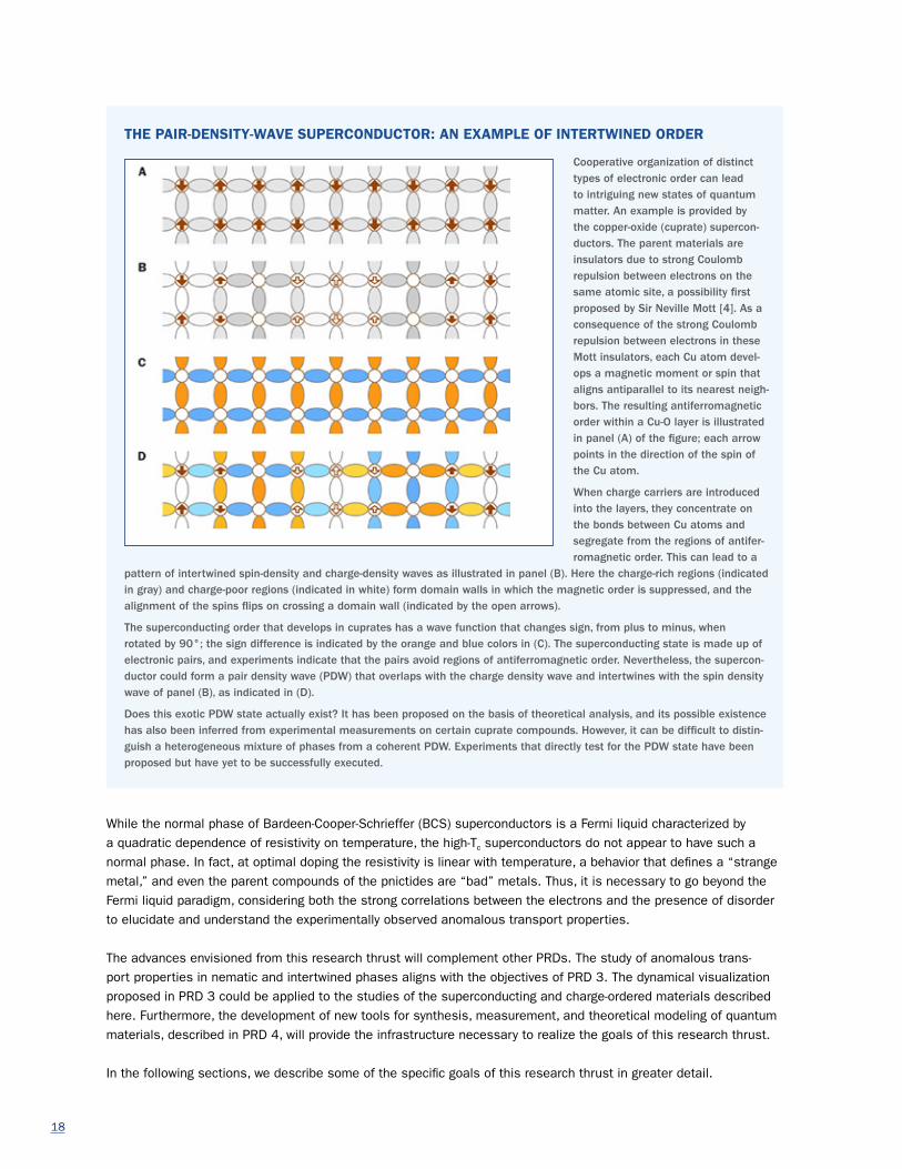
THE PAIR-DENSITY-WAVE SUPERCONDUCTOR: AN EXAMPLE OF INTERTWINED ORDER
Cooperative organization of distinct types of electronic order can lead to intriguing new states of quantum matter. An example is provided by the copper-oxide (cuprate) supercon-ductors. The parent materials are insulators due to strong Coulomb repulsion between electrons on the same atomic site, a possibility first proposed by Sir Neville Mott [4]. As a consequence of the strong Coulomb repulsion between electrons in these Mott insulators, each Cu atom devel-ops a magnetic moment or spin that aligns antiparallel to its nearest neigh-bors. The resulting antiferromagnetic order within a Cu-O layer is illustrated in panel (A) of the figure; each arrow points in the direction of the spin of the Cu atom.
When charge carriers are introduced into the layers, they concentrate on the bonds between Cu atoms and segregate from the regions of antifer-romagnetic order. This can lead to a
pattern of intertwined spin-density and charge-density waves as illustrated in panel (B). Here the charge-rich regions (indicated in gray) and charge-poor regions (indicated in white) form domain walls in which the magnetic order is suppressed, and the alignment of the spins flips on crossing a domain wall (indicated by the open arrows).
The superconducting order that develops in cuprates has a wave function that changes sign, from plus to minus, when rotated by 90°; the sign difference is indicated by the orange and blue colors in (C). The superconducting state is made up of electronic pairs, and experiments indicate that the pairs avoid regions of antiferromagnetic order. Nevertheless, the supercon-ductor could form a pair density wave (PDW) that overlaps with the charge density wave and intertwines with the spin density wave of panel (B), as indicated in (D).
Does this exotic PDW state actually exist? It has been proposed on the basis of theoretical analysis, and its possible existence has also been inferred from experimental measurements on certain cuprate compounds. However, it can be difficult to distin-guish a heterogeneous mixture of phases from a coherent PDW. Experiments that directly test for the PDW state have been proposed but have yet to be successfully executed.
While the normal phase of Bardeen-Cooper-Schrieffer (BCS) superconductors is a Fermi liquid characterized by a quadratic dependence of resistivity on temperature, the high-Tc superconductors do not appear to have such a normal phase. In fact, at optimal doping the resistivity is linear with temperature, a behavior that defines a “strange metal,” and even the parent compounds of the pnictides are “bad” metals. Thus, it is necessary to go beyond the Fermi liquid paradigm, considering both the strong correlations between the electrons and the presence of disorder to elucidate and understand the experimentally observed anomalous transport properties.
The advances envisioned from this research thrust will complement other PRDs. The study of anomalous trans-port properties in nematic and intertwined phases aligns with the objectives of PRD 3. The dynamical visualization proposed in PRD 3 could be applied to the studies of the superconducting and charge-ordered materials described here. Furthermore, the development of new tools for synthesis, measurement, and theoretical modeling of quantum materials, described in PRD 4, will provide the infrastructure necessary to realize the goals of this research thrust.
In the following sections, we describe some of the specific goals of this research thrust in greater detail.
19
Beyond the competing-order paradigm: Strongly-correlated systems are characterized by competing interactions. At a minimum, there is competition between Coulomb repulsion, which tends to localize electrons, and kinetic energy, which favors delocalization. Further complications arise when multiple partially filled orbitals are involved and when coupling to lattice distortions is significant. Competing interactions can lead to a great variety of ordered states, such as spin density waves, various charge density waves, nematic order, current-loop order, and superconductivity.
Superconductivity often appears when the ordering temperature for a different “competing” order, often a CDW or SDW, is driven to zero (defining a quantum critical point, or QCP) as a function of a parameter such as electron-ic-carrier concentration, pressure, or strain. While empirically established, the appearance of superconductivity near some QCPs is not properly understood. There is a strong need to develop improved theoretical models of quantum critical phenomena in strongly-correlated metals and to make firm predictions that can be tested by experiment, from transport properties to order parameter correlations and dynamics. Conversely, there is a need for improved experimental measurements of charge, spin, and lattice dynamics in the vicinity of QCPs to provide clues to theo-rists. In addition, what can we learn from metallic QCPs where superconductivity does not appear? Chemical doping introduces disorder and thus, the effects of disorder near a QCP need to be understood. The possible formation of inhomogeneous states has to be considered when analyzing experimental data and in theoretical work to study and discover potential functionalities.
As an alternative to competing order, there are instances where the active degrees of freedom cooperate to form intertwined orders, such as the CE state of quarter-filled manganites with simultaneous spin, charge, and orbital order. Recent work has introduced the concept of intertwined order in cuprate superconductors [5]. Motivated in particular by the pseudogap phase, various theories have proposed that electronic pair correlations and spin correla-tions may develop together in a cooperative fashion. Similar concepts are relevant to iron-based and heavy-fermion superconductors, as well. There is considerable need to improve the analytic modeling, numerical computation of ground state energies, and evaluation of the dynamics of intertwined orders. One concept involves a proposed PDW superconductor. There is circumstantial evidence for such a state in certain cuprate compounds and in supercon-ducting CeCoIn5 at high magnetic field [6]. Experimental tests of this state are needed, following up on existing theoretical predictions.
In a number of cuprate families, CDW order has been observed to develop within the pseudogap phase and to compete with the onset of superconducting order. Transport studies at low temperature, but in a high magnetic field to suppress the superconducting order, indicate an emergent Fermi-liquid behavior, but with poorly understood electron-like pockets together with some form of CDW order. There is a need to determine the character of this CDW order with x-ray diffraction measurements in the presence of a very strong magnetic field, as well as to probe the high-field behavior of the spin correlations by neutron scattering. Extending other probes, such as optical spectros-copy, to high magnetic fields would also be valuable.
As our understanding of intertwined orders improves, can we use the concept to design new, high-performance superconductors? Going beyond superconductors, can we use the concept to design or discover other important functional materials? In particular, there is a need for improved multiferroic materials, which combine two orders, such as ferromagnetic and ferroelectric polarization, and allow cross-manipulation of the orders, such as the control of ferromagnetic domains with an electric field or the control of ferroelectric domains with a magnetic field. One might also imagine improved thermoelectrics, where the challenge is to maintain good electrical conductivity while minimizing the thermal conductivity.
Nematic electronic phases: Nematic electronic states have been observed in the vicinity of the superconducting phase of high-Tc superconductors. One example occurs in the iron pnictides of the 122 family, where a nematic phase is stabilized upon electron doping. This phase occurs above the Néel transition temperature (TN) and the superconducting temperature, but below the structural transition temperature (TS) at which the lattice structure changes from tetragonal to orthorhombic, as shown in Fig. 2.1.1 [7]. The large anisotropies in the transport proper-ties compared with the small lattice distortion in the nematic phase point to an electronic origin of the effects, but

20
due to the presence of several active degrees of freedom, the mechanism that leads to nematicity remains elusive. It is necessary to resolve whether either the magnetic or the orbital degrees of freedom drive the nematic state or whether this exotic nematic regime results from the cooperative interaction of spin, orbitals, and lattice.
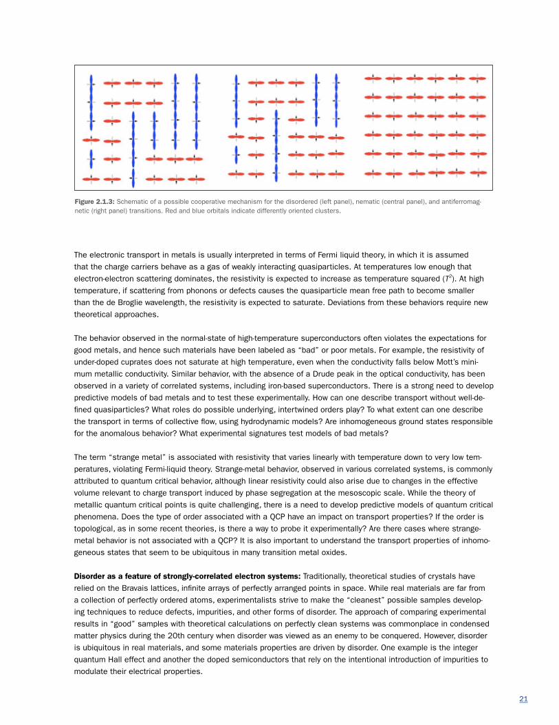
For example, does the nematic transition arise from spin correlations as depicted in Fig. 2.1.2 [8] or is the disor-dered state homogeneous only on average (left panel of Fig. 2.1.3) with a balanced amount of (π,0) (red) and (0,π) (blue) clusters? In this picture, the nematic state occurs when there are more (π,0) than (0,π) clusters (central panel), so that the rotational symmetry is broken before long-range order develops below the Néel temperature (right panel).
Both theoretical and experimental techniques are needed that can differentiate between homogeneous, single-de-gree-of-freedom-driven processes and cooperative mechanisms characterized by intrinsically inhomogeneous states with several active degrees of freedom. On the theory side, new, perhaps phenomenological, model Hamiltonians that include orbital, spin, and lattice degrees of freedom need to be developed as well as novel numerical algorithms to deal with the larger Hilbert space. The results obtained could be used to guide the development of mean-field Ansatz that could eventually be utilized to improve numerical approaches to study microscopic Hamiltonians. The development of new computational methods that retain the multi-electron character of the correlations and allow studying combined and inhomogeneous states as recommended in PRD 4, works synergistically with this component of PRD 1. On the experimental side, synthesis is crucial to understand the dependence of nematicity on doping, such as electron versus hole versus isovalent in-plane and out-of-plane doping, and also to clarify the role of de- twinning processes. Bulk materials and thin films are needed to clarify the effects of dimensionality and thickness and to support the various experimental techniques that are best suited for different types of samples. The vast improvements in efficiency and resolution in experimental probes, such as angle-resolved photoemission spectros-copy (ARPES), neutron and x-ray scattering, electron microscopy, and scanning tunneling microscopy (STM), should continue. Nevertheless, it is necessary to develop new techniques to probe multiple degrees of freedom simultane-ously and the effects of extreme conditions, such as pressure and magnetic field, on the nematic state.
Since the nematic phase is located above the superconducting phase, an understanding of its properties is expected to unveil the role that the spin, the orbitals, and the lattice play in the mechanism that produces high-Tc superconductivity.
Anomalous conductivity in strongly-correlated systems: The electrical resistivity in the normal state of strongly- correlated systems often exhibits behavior that is not well understood. There is a need to develop a proper theoretical understanding of such behaviors, including predictions of unique signatures that can be tested by experiment. In particular, we need a better understanding of how resistivity is related to the underlying charge/spin/orbital/ lattice correlations.
Ba(Fe1-xCox)2As2
150
100
50
00.00 0.02 0.04 0.06 0.08 0.10 0.12
Tet
AFM Ort
TN
Ts
Tc
Ort
SC
T (K
)
X
disordered state
symmetrybreaking
symmetrybreaking
nematic state magnetic state
Z2O(3)
Si S
i+xS
i S
i+yS
i0
Fig. 2.1.1: Ba(Fe1-xCox)2As2 phase diagram. Figure 2.1.2: Schematic of possible magnetic correlations underlying the transition from the disordered to the nematic to the magnetic state. In the nematic state where 4-fold rotational symmetry is broken, the indicated red and blue directions are distinct.
21
The electronic transport in metals is usually interpreted in terms of Fermi liquid theory, in which it is assumed that the charge carriers behave as a gas of weakly interacting quasiparticles. At temperatures low enough that electron-electron scattering dominates, the resistivity is expected to increase as temperature squared (T2). At high temperature, if scattering from phonons or defects causes the quasiparticle mean free path to become smaller than the de Broglie wavelength, the resistivity is expected to saturate. Deviations from these behaviors require new theoretical approaches.
The behavior observed in the normal-state of high-temperature superconductors often violates the expectations for good metals, and hence such materials have been labeled as “bad” or poor metals. For example, the resistivity of under-doped cuprates does not saturate at high temperature, even when the conductivity falls below Mott’s mini-mum metallic conductivity. Similar behavior, with the absence of a Drude peak in the optical conductivity, has been observed in a variety of correlated systems, including iron-based superconductors. There is a strong need to develop predictive models of bad metals and to test these experimentally. How can one describe transport without well-de-fined quasiparticles? What roles do possible underlying, intertwined orders play? To what extent can one describe the transport in terms of collective flow, using hydrodynamic models? Are inhomogeneous ground states responsible for the anomalous behavior? What experimental signatures test models of bad metals?
The term “strange metal” is associated with resistivity that varies linearly with temperature down to very low tem-peratures, violating Fermi-liquid theory. Strange-metal behavior, observed in various correlated systems, is commonly attributed to quantum critical behavior, although linear resistivity could also arise due to changes in the effective volume relevant to charge transport induced by phase segregation at the mesoscopic scale. While the theory of metallic quantum critical points is quite challenging, there is a need to develop predictive models of quantum critical phenomena. Does the type of order associated with a QCP have an impact on transport properties? If the order is topological, as in some recent theories, is there a way to probe it experimentally? Are there cases where strange-metal behavior is not associated with a QCP? It is also important to understand the transport properties of inhomo-geneous states that seem to be ubiquitous in many transition metal oxides.
Disorder as a feature of strongly-correlated electron systems: Traditionally, theoretical studies of crystals have relied on the Bravais lattices, infinite arrays of perfectly arranged points in space. While real materials are far from a collection of perfectly ordered atoms, experimentalists strive to make the “cleanest” possible samples develop-ing techniques to reduce defects, impurities, and other forms of disorder. The approach of comparing experimental results in “good” samples with theoretical calculations on perfectly clean systems was commonplace in condensed matter physics during the 20th century when disorder was viewed as an enemy to be conquered. However, disorder is ubiquitous in real materials, and some materials properties are driven by disorder. One example is the integer quantum Hall effect and another the doped semiconductors that rely on the intentional introduction of impurities to modulate their electrical properties.
Figure 2.1.3: Schematic of a possible cooperative mechanism for the disordered (left panel), nematic (central panel), and antiferromag-netic (right panel) transitions. Red and blue orbitals indicate differently oriented clusters.

22
In the quest to under-stand quantum materials,the effects of disorder are often neglected by theo-rists even though many interesting properties of quantum materials, such as high-Tc superconduc- tivity, occur upon chemicaldoping, which necessarily introduces disorder. For example, experiments performed in half-dopedmanganites under con-trolled disorder showedthat in the ordered com-pound a first-order phase transition separates the ferromagnetic (FM) from the antiferromagnetic (AF) phase as predicted by
theory in the “clean” limit. The disordered compound has a drastically reduced Curie temperature as seen in the left panel of Fig. 2.1.4. However, the most remarkable feature is that the phenomenon of colossal magnetoresistance (CMR), where small magnetic fields induce drastic changes in resistivity, only appears in the disordered sample as shown in the right panel of Fig. 2.1.4. This indicates that disorder is needed for CMR to occur. Could it be possible that disorder is not a foe and that some of the most exciting properties observed in transition metal oxides and other quantum materials may actually be caused by imperfections and defects?
To investigate quantum materials in this new light, synthesis with controlled defects and dopants has to be pursued. In addition, the intentional introduction of defects could be used as a spectroscopic tool to explore the interactions that drive the formation of spatially ordered states as well as the relationship between these phases and other electronic states present in the material at lower tempera-tures, extreme pressures, or high magnetic fields. Another direction to be followed is particle irradiation, which provides a controlled way of inducing different kinds of defects, from uniformly spaced point defects to complex defects such as cascades and columnar defects. An advantage of introducing defects by radiation, as opposed to chemical doping, is that the lattice constants are less affected. Another avenue to be considered is doping via ion implantation in materials that are difficult to dope chemically, such as antiferromag-netic Sr2IrO4. The latter has been doped by implantation of K ions providing a potential novel path to the realization of superconducting
states [10]. Ion implantation can also be used to induce strain as in the case of He implantation in La0.7Sr0.3MnO3 The controlled introduction of disorder can be used as a technique to study the evolution of an observable, such as the superconducting gap, which may help unveil the symmetry of the Cooper pairs.
Another possible effect of disorder that should be explored is the anchoring of vestigial phases. The cartoon in Fig. 2.1.5 shows how a nematic phase can be anchored by non-magnetic impurities indicated by the circles. The majority red clusters have (π,0) magnetic order and locally break rotational invariance. But long-range magnetic order does not develop because the (π,0) clusters separated by the impurities are magnetically out of phase.
Figure 2.1.5: Cartoon depiction of a nematic phase of spin (arrows) and orbitals (red and blue) stabilized by non-magnetic impurities (circles).
Figure 2.1.4: On the left is a phase diagram of Ln1/2Ba1/2MnO3 for both ordered and disordered struc-tures. On the right are transport properties of the ordered (top) and disordered (bottom) structures. Only the disordered case shows the CMR effect.
600
500
400
300
200
100
0
0.20
0.15
0.10
0.05
0.00
1.0
0.5
0.0
102
101
100
10-1
102
101
100
10-1
10-2
1.20 1.25 1.30 1.35 0 100 200 300 400
Ionic radius of Ln (Å)
Tem
pera
ture
(K
)
Temperature (K)
Mag
netiz
atio
n (µ
?/M
n si
te)
Resistivity (Ω
cm)
Y Dy Tb Gd Eu Sm Nd Pr La
Ln1/2Ba1/2MnO3
Tco
a
b
Tc
TcTN
TN
TSG
Ordered
Disordered
CO/OO
AF(A) FM FM
+SGSG
Nd1/2Ba1/2MnO3
Ordered
Disordered
1 kOe ZFC
0 Oe10 kOe50 kOe70 kOe
FM

23
In order to include the effects of quenched disorder in theoretical studies of quantum materials, it is necessary to develop real space approaches. New order parameters, involving several degrees of freedom, have to be proposed for states with broken symmetries and no long-range order. Hybrid techniques combining mean-field approximations with Monte Carlo simulations could provide a path to study the large systems needed to explore inhomogeneous states. The effects of disorder in the multiple parameters of model Hamiltonians, such as hopping amplitudes, magnetic couplings, on-site chemical potentials, etc., need to be calculated for different kinds of impurities. On the experimental side, it will be necessary to develop techniques with enhanced real space resolution to determine the properties of the ground state as a function of the location and density of defects and impurities.
Thrust 1b: Predict, Realize, and Probe New States of Quantum Magnets
Three different axes can be used to identify quantum phase transitions in quantum materials beyond the conven-tional paradigms: symmetry, topology, and metallicity. Symmetry encapsulates the conventional characterization of phases in terms of ordering of atomic positions, magnetic moments, and other local properties. Metallicity describes the tendency for electronic delocalization and the formation of Fermi surfaces or more exotic singularities in momentum space. Topology is the newest addition to this characterization; quantum spin liquids with no broken symmetries are characterized by the topology of their wave function, which is invariant under local perturbations but responds to global changes. Quantum phase transitions and quantum critical points are associated with transitions between the various regimes in this description.
This leads to three different directions for progress in quantum magnetic materials: the metallization of quan-tum magnets, the destabilization of quantum magnets, and the taming of entanglement in quantum magnets. Metallization probes the connections between valence bonds and Cooper pairs: Can we realize novel forms of superconductivity, potentially at high temperatures? The destabilization of quantum magnets (i.e., “magnets on the verge”) explores the creation of novel states with long-range entanglement through the frustration or weakening of magnetic correlations. Taming entanglement involves using recent developments in the understanding of entangle-ment to characterize quantum states and pave the way for new probes and applications.
Scientific objectives: A defining feature of systems with interacting electrons is the presence of different ground states with long-range order in the charge, orbital, or spin degrees of freedom. The onset of order is traditionally associated with the breaking of a fundamental symmetry, in turn producing new classes of ground states and exci-tations. These phase transitions are driven by correlations in space and time that diverge at the critical point. There has been much interest in understanding how these critical points evolve as finite temperature transitions are suppressed to zero temperature, becom-ing “quantum critical points,” which may be exploited to achieve novel material behaviors through an extended range of temperatures.
A major shift in this paradigm has occurred in recent years, due to the rising appreciation that some phases of matter are described by more than the formation of spatially ordered patterns of neatly aligned magnetic dipoles or periodically arranged atoms. Certain states of matter resist characterization in terms of a local quantity such as spontaneous magnetization or the superfluid phase. Instead, these are distinguished by global properties known as topological invariants. Whereas conventional phase transitions have a local order parameter present on one side of the transition and absent on the other, topological phase transitions are accompanied by a discontin-uous change in a global topological invariant such as the Chern num-ber of electronic energy bands or the global flux of an emergent gauge
Symmetry Metallicity
Topology
Figure 2.1.6: Different types of quantum fluids can be realized depending on the balance of broken symmetries, topological character, and degree of metallicity. For instance, a fermionic quantum critical point is found when a symmetry is broken in a metal on the verge of electronic delocalization. A topological superconductor may occur when the quantum fluctuations associ-ated with a frustrated lattice are so strong that magnetic order is no longer possible. The onset of metallicity in a system with strong topological character may proceed through the formation of a Weyl semimetal.

24
field. Elementary excitations in these phases of matter may have fractionalized quantum numbers and may exhibit anyonic statistics as exemplified by charge e/3 quasiparticles in the fractional quantum Hall state at 1/3 filling. Magnetic monopoles in spin ice are a clear example of fractionalization of the original degrees of freedom (magnetic dipoles) in a magnetic system. Quantum spin liquids are a new class of topologically ordered phases of magnetic matter, constituting a new frontier for both theorists and experimentalists (see the sidebar “Towards a Taxonomy of Quantum-Entangled Magnetic States”). Such systems provide a rich variety of qualitatively new collective states of matter. Ultimately, they may also form the basis for groundbreaking applications, such as in decoherence-resistant quantum computing.
A wide variety of topological behaviors can occur, and topological behavior does not preclude more traditional forms of order. What is needed is a new and holistic approach to the description of phase transitions that encompasses both symmetry and topology. This new approach will allow us to understand and even control the stabilities of collective phenomena in electronic matter. Also importantly, this approach will allow us to access novel states where the nature of the order defies conventional classifications and is thus — for now — “hidden.” Fig. 2.1.6 offers a schematic to help understand the interplay between symmetry and topology, whether electronic correlations are strong enough to localize electrons in insulators or weak enough to induce fluids of delocalized but interacting electrons in metals. Much experimental and theoretical effort has focused on systems that are close to instability, for instance, the suppression of long-range magnetic order by pressure, composition, or magnetic field to form a T=0 phase transition that is called a QCP. The collapse of the magnetic order parameter leads to a plethora of low-energy excitations that are the proto-material for the stabilization of new phases, most notably unconventional superconduc-tivity. In some cases, electronic delocalization may accompany the magnetic QCP, increasing the number of states contained by the Fermi surface. Examples include the Mott transition in transition metal oxides and pnictides, the α−γ transition of certain f-electron based systems, and in the Kondo effect of both dilute and concentrated d- and f-electron based systems. It remains a central, and as-yet unanswered, question whether the quantum critical fluctu-ations associated with the stabilization of unconventional superconductivity are entirely those of the T=0 magnetictransition or whether the fluctuations between states with large (delocalized electrons) and small (localized elec-trons) Fermi surfaces are also required. Despite rather overwhelming evidence that QCPs are a feature of virtuallyevery class of material with strong correlations, at present, there are few examples of systems where a detailedcomparison of experimental results such as scaling relations and exponents, or perhaps fundamental charge andmagnetic susceptibilities, can be directly compared to either exact or phenomenological theories. Making this exper-iment-theory connection, analogous to the establishment of universality classes for second order transitions occur-ring at nonzero temperatures, remains an area of great importance that demands advances on the parts of boththeory and experiment. Importantly, it seems likely that a number of systems are already known where order can besuppressed successfully to T=0 without introducing significant disorder or other complications, and where the avail-ability of large high-quality single crystals makes it possible to deploy the most powerful experimental techniques.
A second type of phase transition (depicted between the blue and green regions in Fig. 2.1.6) is from a state with a broken symmetry such as magnetic order to a state where this order is suppressed to T=0 by some sort of frustra-tion, yielding a quantum spin liquid whose excitations and defects have intrinsic topological character. In the last ten years, physicists have made great progress toward finding magnets whose ground states can be described as a quantum spin liquid, a state of matter without the usual magnetic order but with a hidden topological order and fractionalized elementary excitations. Of particular interest is the identification of new systems where the excitations are non-local objects called non-abelian anyons, which are introduced into a system via an operation that flips a large number of spins along a line extending all the way to the boundary. Curiously, an anyonic excitation only appears at the end of this line (a “string”). These string ends behave like particles with nontrivial quantum statistics. Whereas magnons are bosons, particles in 2D spin liquids are generally anyons of various kinds, e.g., in Kitaev’s model they are Majorana fermions and π fluxes.
Theorists have found analytical and numerical arguments that the Heisenberg antiferromagnet on the 2D Kagomé lattice is one such system: Solid-state chemists and physicists have succeeded in growing high-quality crystals with this magnetic lattice, most notably herbertsmithite ZnCu3(OH)6Cl2. Experimentalists have demonstrated the lack of magnetic order, the presence of a spin gap, and diffuse inelastic scattering consistent with fractionalized spin
25
excitations [11]. However, a full understanding of the nature of this spin liquid remains elusive: We do not know the nature of elementary excitations and currently lack experimental probes for their identification. A serious problem is the current gap between theories of strongly correlated matter and experimental probes capable of testing them. As will be discussed further below, entanglement entropy is a central theoretical tool; it would be a significant advance to discover an experimental way to access it.
Here too, the advancement of the field depends on the discovery of new frustrated systems that are available in the form of large defect-free samples where the ground state can be confirmed, and where this behavior is present under experimentally accessible thermodynamic conditions so that elementary excitations can be studied spec-troscopically. We note that there are potentially interesting possibilities in engineered magnetic materials such as artificial spin ice, which is a 2D network of ferromagnetic nanowires. These nanomaterials can potentially be used in applications like magnetic logic and memory based on mobile domain walls, provided that it is possible to devise fast and reliable ways of injecting, pinpointing, and moving topological defects and to theoretically understand their structure and dynamics.
The third trajectory (depicted between the blue and yellow regions in Fig. 2.1.6) involves the passage from insula-tor to metal in systems with topological character. A prime example of this would be Weyl and Dirac semimetals, which occur when symmetry precludes hybridization where two bands cross near the chemical potential. Unlike a conventional semimetal, a Weyl semimetal occurs when either or both of time reversal and inversion symmetries are broken, and when spin-orbit coupling is large. Weyl semimetals have topologically protected surface states and unusual magnetoelectric transport properties that have been recently discovered in materials with broken inversion symmetry [12, 13]. What is more, their low-energy electronic degrees of freedom resemble massless chiral fermions introduced by Weyl. Weyl semimetals can also be realized in a multilayer system composed of a topological insula-tor and a normal insulator or even a bulk magnetic insulator, such as a pyrochlore iridate, as long as time-reversal symmetry is broken [14, 15].
It is fair to say that the transition between topological insulator and unconventional metal is the least well under-stood and studied of the three property intersections represented in Fig. 2.1.6. The lack of materials where the full transition can be studied as a function of a parametric variable such as composition, pressure, or strain is a current impediment to developing this understanding. In particular, no materials have been identified with topological char-acter where magnetism or strong electronic correlations may be at play in stabilizing a Fermi surface (or Fermi arc in the case of Weyl semimetal) or may have consequences for bulk or surface states. Identifying such materials would constitute a significant breakthrough.
Research opportunities: The last decade has seen a number of significant advances in the area of quantum magne-tism. These include the detection of magnetic monopole dynamics in spin ice [16–21] and the discovery of numer-ous quantum spin liquid candidates based on indirect probes of spin dynamics and quasiparticle fractionalization [11, 22–25]. The frontiers are, simply put, to understand, design, and harness the wealth of novel emergent states that arise from quantum magnetism.
Progress in this field rests heavily on the discovery and development of new material systems where different types of frustration are present, due to low dimensionality, the geometric lattice, or competing long-range interactions. While it was formerly believed that small moments, such as the spin-1/2 Cu2+ are needed for quantum fluctuations to be appreciable, there is mounting evidence that the large moments produced in f-electron based compounds by strong spin-orbit coupling can act like pseudo-spin ½ systems, where an orbital exchange interaction produces the needed low energy scale for the quantum fluctuations [26–29]. Neutron scattering experiments have long been a crucial tool in establishing the basics of quantum spin liquid behaviors: the absence of long-range order, the presence of fractionalized excitations, and the onset of the magnetic gap. It is a characteristic of this field that interesting physics is found on all energy scales: from relatively high to low energy scales. In high energy scales, the interplay between crystal fields and spin-orbit coupling determines the properties of individual magnetic moments. At lower energies, a sequence of diminishing energy scales associated with exchange and dipolar interactions among the moments and interchain or interplanar interactions ultimately may stabilize an ordered phase. As advances are

26
made on the materials side in finding systems where these phenomena are pushed to lower and lower energies, and an extended range of temperatures emerges where the fundamental excitations of a putative quantum spin liquid can be explored, it becomes increasingly important to improve spectroscopic tools based on neutrons, photons, and electrons that probe dynamic spin correlations throughout the relevant range of energy. What is more, these quan-tum critical systems seldom form at exactly the critical conditions where order vanishes. Consequently, non-thermal tuning parameters such as pressure, magnetic field, or composition must be employed to drive materials to the crit-ical point or from one regime to another. The ability to probe magnetic excitation spectra of materials at high fields or perhaps high pressures, at temperatures that are both above and below the energy scale in question, and in ways that link directly to theory is thus essential for further progress.
Substantially less is known about the quantum critical charge response, although optical spectroscopy, resonant inelastic x-ray scattering, and photoemission measurements are increasingly brought to bear. These measurement techniques must also be improved to access a full range of energy scales. Efforts to extend advanced spectroscopic methods to lower temperatures, and if possible to high fields or high pressures, will be important to explore new materials, regimes, and phenomena.
Some of these specific research directions are described in greater detail in the following sections.
Metallizing quantum magnets: One of the important pathways to new quantum states of matter is to inject mobile charge into quantum spin liquids. The singlet spin pairs that dominate a quantum spin liquid closely resemble Cooper pairs in superconductors. One of the predictions of P. W. Anderson’s Resonating Valence Bond (RVB) theory of high-temperature superconductivity is that when charge is injected into a spin liquid, the pairs from the spin liquid will provide the strong singlet correlations necessary for the formation of a superconducting material [3]. At the very least, it is believed that new kinds of metallic states can emerge from doped spin liquids, with a strong susceptibil-ity to developing new kinds of order, including superconductivity. For this reason, discovering new candidate mate-rials for quantum spin liquids that can be produced from states with conventional order, via doping, pressure, or strain, are an important goal of current research.
Though experimentalists have successfully injected charge into quantum antiferromagnets and spin liquids via doping, none have proven to be metallic. The understanding of why the dopant holes are not mobile is a question of fundamental importance. One idea is that disorder localizes the narrow band mobile electrons inside the spin liquid. The narrow band character of the holes injected into the antiferromagnet makes them extremely prone to Anderson localization by disorder, giving rise to an insulating rather than a metallic state. The development of new strategies to understand and overcome the localizing effects of disorder is a high priority.
Strategies for successful metallization may involve the use of spin-liquid materials built out of broader-band elec-trons or with weaker on-site Coulomb interactions (the high-temperature cuprate superconductors may lie in this class). Recent work in the area of cluster magnets has shown promise, for example, in the discovery of quantum magnetism in LiZn2Mo3O8 [24, 25] and a transition from magnetic to metallic (and superconducting) state with pressure in GaNb4Se8 [30]. These systems are distinguished by having unpaired magnetic electrons, in states that are delocalized over a small cluster of metal atoms (e.g., one S=1/2 per Nb4 or Mo3 unit), placing them closer to the fully delocalized limit.
Another promising route to the metallization of spin liquids is to embed the spin liquid within a metallic host. While this type of electronic structure can be realized in transition-metal based metals with magnetic moments derived from quasi-localized d-electrons lying on frustrated Kagomé lattices [31], they are much better known in f-electron materials. The f-electron materials involve a dense lattice of local magnetic moments immersed inside a conducting fluid (see Fig. 2.1.7). Metallic quantum spin liquids with fractionalized excitations have been achieved by placing large rare earth moments on frustrated pyrochlore lattices [27–29] or on decoupled spin chains [26].

27
Recently, a new family of frustrated f-electron materials has been discovered in which the f-electrons are prevented from magnetic ordering, through magnetic frustration. An example of such a material is CeRhSn — a strange non-Fermi liquid metal that is attracting much attention [32].
Another aspect of the metallized magnetic behavior of f-electron materials concerns the possibility that the entan-gled spin and conduction system can give rise to a topologically ordered insulating or even superconducting state. These materials extend the concept of topological order into the realm of strongly interacting electron systems. Such topological Kondo insulating behavior was theoretically predicted [33, 34] and has been tentatively confirmed in SmB6 [35–38] and also YbB12 [39, 40] through the observation of robust conducting surface states. Also, the Kondo semi-metal CeNiSn, when doped with Sb, has been proposed as a possible Mobius Kondo insulator [41, 42]. In these new classes of material, the juxtaposition of magnetic and topological properties has the potential to drive new types of behavior, such as the spontaneous development of superconductivity in the topological surface states.
Quantum magnets on the verge: The basic recipe for making a new class of quantum spin liquids is to weaken or eliminate magnetic order by increasing quantum fluctuations. One well-known method to achieve this is to place spins on a lattice that frustrate conventional magnetic order. When there is an extensive manifold of low energy states, there will be strong quantum fluctuations among these states. This strategy worked very well in the case of herbertsmithite, a Kagomé lattice spin liquid [11, 22, 23]. Another promising route to suppressing magnetic order is to alter the Hamiltonian either with new terms or by weakening the magnetic tendencies through a smaller on-site Coulomb interaction (U). Starting with a simple Hubbard Hamiltonian with hopping amplitude (t) and on-site U, one can add terms such as longer-range hopping (t’), Coulomb repulsion between electrons on neighboring atoms (V), spin-orbit coupling (λ), and intra-atomic exchange (JH). Tuning these additional terms with respect to U may reveal an unexplored regime of quantum matter. For example, a simple square lattice quantum antiferromagnet could become a spin liquid in the presence of sizable second nearest neighbor interactions, arising from the longer-range hopping t’ [43–45]. Another example is the axionic insulator phase that can be stabilized by tuning V against U [46]. Of particular interest is the spin-orbit coupling, which opens an exciting new dimension in quantum magnetism [47]. Fig. 2.1.8 shows a phenomenological phase diagram of electronic materials that has been theoretically established in terms of the electronic interaction strength, U/t, and spin-orbit coupling strength, λ/t. At low λ/t, the system transitions from a metal to a Mott insulator, where on-site Coulombic repulsion localizes the electrons and leads to localized magnetic states. If the geometry of the underlying magnetic lattice is low dimensional or frustrated, then
Figure 2.1.7: The f-electron compounds contain a dense lattice of spin-orbit coupled magnetic moments, derived from electrons bound deep inside f-orbitals. The immersion of these moments within a sea of mobile electrons as indicated in (A) causes the electronic and magnetic degrees of freedom to mutually entangle, profoundly transforming the material and (B) shows one possible outcome, where the f-electrons become part of the Fermi liquid with itinerant “heavy fermion” quasi-particles indicated. Suitably tuned, the process can alsolead to quantum criticality, new types of metallic behavior, and new forms of quantum order including superconducting and multipolar order.It can also give rise to insulators where topology and magnetism are intertwined. Such materials may have strongly interacting electrons intopologically protected surface states.
A B

28
novel quantum magnetic states (such as spin liquids) may emerge. Indeed, this is the regime where many of the quantum materials that attracted attention in thepast decade were found. New rich quantum magnetic phenomena are predicted to occur when spin-orbit coupling is no longer negligible. For example, there is the possibility of spin liquid states in the absence of geometric frustration. These spin liquid states are due to anisotropic bond-dependent exchange interactions or magnetic states that behave as axions and that can be used to measure fundamental quantities of the universe such as the fine structure constant. (Axions are particles postulated in high-energy physics to resolve the strongcharge-parity [CP] problem.) In heavy transition metal compounds with electrons in 4d or 5d orbitals, orbital and spin degrees of freedom are locked together by strong spin-orbit coupling. Since the magnetic “spin” wave function now looks anisotropic because of the
involvement of orbitals, hopping amplitudes will depend strongly on the bond direction [48]. The resultant bond-depen-dent exchange interaction is an integral ingredient of the Kitaev honeycomb model, whose ground state is a quantum spin liquid [49]. Therefore, tuning of spin-orbit coupling is a promising route to new forms of dynamic quantum matter. It should also be noted that structural details matter, since crystal field splitting due to distorted crystal structure can quench the requisite orbital degrees of freedom. On the other hand, even if the bare value of λ is small, a highly symmetric octahedral environment can accentuate the spin-orbit effect as demonstrated for α-RuCl3 [50].
Although extensive research efforts are focused on spin-orbit driven quantum magnetism in iridates, very limited studies have been carried out for other 5d compounds. The physics of iridates is in principle simple since an effec-tive one-band model can describe their electronic structure in the absence of significant intersite interactions [51]. However, when the overlap between orbitals on adjacent iridium ions is non-negligible, or when the electron count of the t2g set is d4, d3, or d2, a multi-band description is required to understand the electronic and magnetic states. The multi-band description includes both instability to the formation of metal-metal bonds and Hund’s rule coupling (JH). For example, d4 in an octahedral crystal field should form an S=1 state due to Hund’s rule coupling, but strong spin-orbit coupling or non-negligible orbital overlap between sites will make it non-magnetic due to the formation of an intra-atomic J=0 state or metal-metal bonding, respectively. Competition between these interactions in different frustrating lattice geometries should be fertile ground for the discovery of qualitatively new spin-orbital states of matter [52].
Experimentally tuning these energy scales is a challenging task. A carefully designed materials strategy will be important to vary the effective spin-orbit coupling, λ, since 5d, 4f, and 5f elements naturally provide large λ values. To change the values of t’ and V, hydrostatic pressure, uniaxial strain, and direct chemical control of the bonding geometry may be applied. Organic and cluster based magnetic materials provide fertile potential for applications due to their high compressibility [53, 54].
Taming entanglement in quantum magnets: The last decade has seen the emergence of a plethora of quantum spin liquid candidates in two and three dimensions, from the Kagomé-lattice herbertsmithite to the organic magnets with a triangular lattice of spins and quantum spin ice in the pyrochlore Yb2Ti2O7 [21, 22, 53]. Considerable prog-ress has been made on the theoretical side with the advent of exactly solvable models of quantum spin liquids with strong entanglement, an emergent gauge field, and fractionalized excitations [50] and the identification of several compounds, where this particular state of matter may be realized [48, 49]. Strong evidence for a quantum spin liq-uid with an emergent Z(2) gauge field has been found in several numerical and theoretical studies [55, 56]. A chiral spin liquid, resembling the quantum Hall state of bosons at ½ filling, has been identified in some theoretical models [57]. However, positive experimental identification of a quantum spin liquid has remained elusive so far. Part of the
U/t
λ/t
Top. ins.or semi-metal
Simplemetal orband ins.
Spin-orbit coupledMott ins.
Mott ins.
Axionins.
Spin-liquid Quadrupolar
Weylsemi-metal Top.
Mott ins.
Figure 2.1.8: Sketch of a generic phase diagram for electronic materials, in terms of the interaction strength U/t and spin-orbit coupling λ/t.

29
problem is the difficulty of numerical simulations, which have only recently been able to identify spin liquid phases [55, 56], but which are still limited in their ability to predict experimentally accessible physical properties such as spin spectral functions. There is also a dearth of exactly solvable theoretical models, which besides potentially yielding specific predictions for experimentally measurable quantities might also help guide simulations, which need substantial interpretation because of finite size effects and other computational limitations. Consequently, an area of urgent research interest is to develop the experimental, theoretical, and computational tools needed to identify quantum spin liquids in two and three dimensions.
One can envision two ways of bridging this gap between theory, computation, and experiment. First, we should aim to predict signatures of quantum spin liquids for the existing experimental probes. This will require continued development and improvement of theoretical and computational techniques. Second, we should aim to develop new experimental ways of directly probing the defining characteristics of quantum spin liquids, such as strong quantum entanglement of local degrees of freedom. Recent work in the area of topological corrections to entanglement entropy and in the analysis of patterns in reduced density matrix eigenvalues (the “entanglement spectrum”) have had substantial impact on simulations, but do not appear to be experimentally accessible. Similar characteristics must be found which are measurable in the lab.
A particularly compelling goal is direct experimental evidence for exotic quasiparticles with anyonic statistics thought to be inherent to at least some of quantum spin liquids in two dimensions. These anyons can exist as intrinsic elementary excitations of the physical system or arise in response to extrinsic perturbations such as “twist” dislo-cations [58]. Aside from being fundamentally interesting physical objects, the realization of such quasiparticles in a crystalline solid could be a step toward realization of topological quantum computation via anyon braiding [59]. Another exciting avenue of research is to determine the experimentally observable consequences of spin liquid behavior in the charge domain. For example, there are recent proposals that physics similar to the magnetic mono-poles in spin ice might appear in charge ice.

30
2.2 PRD 2 — HARNESS TOPOLOGICAL STATES FOR GROUNDBREAKING SURFACE PROPERTIES
Topological quantum materials show a new kind of electronic order with great potential to improve existing
electronics and create entirely new kinds of devices. Most of the scientific excitement and potential utility of
topological materials can be traced back to two properties: They can support large, switchable electronic surface
current with low energy loss, and they host fractional “quasiparticles” with qualitatively different properties than
the original electrons. In recent years, there has been remarkable growth in our ability to create and manipulate
topological states of electrons. While it is always hard to predict how basic research will propel science and
technology, experience shows that improving material properties and the design of new materials has a high
probability of opening new frontiers. Additionally, the development of new measurement techniques and func-
tional nanoscale structures has the potential of revolutionizing our ability to understand and exploit physical
phenomena. These areas, therefore, are the focus of the two thrusts that make up this PRD.
2.2.1 Introduction
The dramatic properties of topological phases have the potential to revolutionize electronics. While topological phases of electrons have been studied since the 1980s, our ability to create them in a wide variety of materials has exploded in the past few years. They possess a different kind of order than conventional materials, and the same features that make this order detectable and scientifically interesting also give it great potential for energy- relevant technologies.
The first high impact property of topological phases is that they can show dissipationless transport (i.e., electrons can carry a current without energy losses). The absence of dissipation as electrons move along the edges or surfaces of a topological phase is what leads to the fantastically precise value of conductivity in the earliest topological phase, the quantum Hall effect. The dissipationless transport in a topological edge or surface state is similar in principle to that in a superconductor. Considerable effort was invested in developing small, extremely fast computing devices based on superconductivity however various challenges, including the need to maintain cryogenic temperatures, may explain why such devices are not yet in widespread use. Topological phases seem likely to be much easier to work with than superconductors for several reasons. They may not require as low temperatures as superconductors. Also, in some cases, the dissipationless transport is more easily switchable by applied electric or magnetic fields. Dissipation and heating present major challenges in current computing devices as the feature size of interconnects and logic elements reaches the nanoscale; topological materials offer a new approach to enhance efficiency.
Topological materials offer new approaches to the computing process itself. They can be highly switchable by applied fields through a different mechanism than existing transistors, whose switching underlies the modern central processing unit (CPU) used in computers today. An even more ambitious set of goals concerns the use of topological materials in a quantum or neuromorphic computer. A topological quantum computer is based on a second remarkable property of topological phases, that they host new particles (quasiparticles) that are fundamentally differ-ent from the ordinary electron. Typically these quasiparticles are fractional in that it takes several of them to make up an ordinary electron. Aside from fractional charge, they have other surprising properties, some of which have already been seen in experiments and will facilitate the design of a robust quantum computer that is insensitive to noise.
31
Considerable work will be required to improve topological materials if their dissipationless transport and fractional quasiparticles are to be useful. Perhaps most important will be the development of new device concepts with the potential to supersede existing electronics. Topological materials present an ideal case where fundamental scientific discoveries are also well suited to potential applications in the medium term.
2.2.2 Scientific Challenges
The scientific challenges in this field can be grouped broadly into finding new kinds of topological materials and finding new platforms to probe and exploit topology. Some topological materials can be understood in a picture of independently moving electrons, somewhat like conventional semiconductors but with additional complications such as spin-orbit coupling: the fact that a rapidly moving electron feels a force that links its internal angular momentum (“spin”) to its motion through space. The notion of topology in such materials can be understood as a knotting or winding of the electron’s quantum wavefunction. For this category of materials, predictive theory has been extremely valuable in identifying potential candidate materials for experiments such as ARPES and tunneling that can directly detect topological features.
There are many other kinds of topological materials that show strong connections with other materials classes dis-cussed in this workshop. For example, we know from theory (and indirectly from the example of superfluid helium-3) that a superconductor can in principle also be topological, and finding examples of topological superconductivity is a high priority. A magnet can also be topological, as in the case of spin liquids where only the spin of the electron, rather than its charge, forms the topological phase.
A key part of the search for complex and potentially useful topological order is the creation of new experiments, along with better strategies for existing experiments, to probe topology in materials. For example, the search for a topological superconductor is proceeding not just by looking for new materials but also by combining existing materials into nanoscale heterostructures, e.g., putting a non-superconducting topological material on top of a non-topological superconductor.
One reason why there is so much interest in these examples of topological order beyond the independent-electron paradigm is that they support the fractionally charged quasiparticles that may be useful for quantum computing. Their technological relevance stems from an amazing property that these quasiparticles are believed to have. All the fundamental particles in nature fall into one of two categories: bosons, such as the photon and Higgs boson, and fermions, such as the electron, proton, and neutron. They are distinguished by how the quantum wavefunction behaves when two identical particles are “braided” (moved around each other).
We now understand, and in a few cases can see by indirect experiments, that quasiparticles in topological phases are neither bosons nor fermions but rather anyons, which show a subtle property of fractional statistics under braid-ing; this behavior is at the heart of their utility for quantum computing. Improving our ability to control and use the unique properties of topological phases, from dissipationless transport up to the braiding of fractional quasiparti-cles, is a major scientific challenge, but the rapid rate of progress in recent years gives reason to believe that it is a feasible one.
2.2.3 Research Thrusts
There are remarkably many frontiers of research in topological quantum materials. Our approach in this section is to give an overview that first focuses on the different classes of topological materials and phases (Thrust 2a), includ-ing the possibility of “bottom-up” engineering of topological phases by combinations of existing materials. We then turn to the problem of how experiments can be carried out to detect topological phenomena, including the creation of new platforms to create and measure excitations with fractional statistics (Thrust 2b). Progress in these directions will contribute to the energy relevant scientific challenges described above.

32
Thrust 2a: Discover New Topological Quantum Materials
New materials will be the basis for harnessing groundbreaking topological states as called for in PRD-2. From bulk materials with free and interacting quasi-particles to heterostructures that rely on proximitizing or bandstructure engineering, close interaction between synthesis and theory is pivotal here so this area approaches the aspiration of “materials by design.”
Non-interacting topological insulators and semimetals: The field of topological quantum materials has benefitted enormously from close connections between theoretical and experimental work. Many of the non-interacting topolog-ical states were first predicted by theory, and later realized in experiments. This is the case for topological insulators and Dirac and Weyl semi-metals. This healthy exchange should continue. For instance, this exchange may lead to new paths to attain Weyl semi-metals. Theory has shown that Weyl electrons may be quite pervasive in broad classes of materials. However, one need not start with Dirac and Weyl semimetals. For example, the application of a magnetic field to a class of semimetals that have a zero energy gap (e.g. HgCdTe, half-Heuslers, and gray tin) converts the conventional Schrödinger states into Weyl states. A second possibility is to start with narrow-gap semiconductors that lack inversion symmetry. Theory predicts that if the energy gap is forced to close (by application of pressure, for example) a metallic state featuring Weyl fermion states should appear. Weyl semimetals may be the source of super-conducting states with novel topological properties. Finally, the layered chalcogenides may be a rich source of topological and Weyl materials. The realization of Dirac states in an antiferromagnet (e.g., CuMnAs) may lead to Weyl states with broken time-reversal symmetry. Moreover, specific combinations of layered materials with known and characterized properties may lead the way to engineer topological and Weyl materials with desired properties.
Topological superconductors (TSCs): Unlike insulators in which the total number of electrons is conserved, super-conductors (and superfluids) spontaneously break the U(1) symmetry associated with the fermion number conserva-tion. Only the fermion number parity (i.e., even or odd) is conserved in the mean-field theory of superconductivity. This important difference in symmetry called for a new topological classification of superconductors different from insu-lators, which was systematized [60, 61] and led to the theoretical finding of a wide class of TSCs. Several concrete examples of TSCs appeared in early model studies [62–65]. However, at present there are only very few possible experimental examples of TSCs; the search and synthesis of such materials must continue.
In the simplest case, one defines a TSC as a fully gapped Bardeen-Cooper-Schrieffer (BCS) superconductor that can-not be adiabatically connected to a Bose-Einstein condensate (BEC) of Cooper pairs [62]. This would be analogous to the topological insulator (TI) that cannot be adiabatically deformed to the so-called atomic limit, where the unit cells are completely separated. By this standard, conventional s-wave spin-singlet superconductors are clearly non-topolog-ical, because they exhibit a smooth crossover from the weak-coupling Bardeen-Cooper-Schrieffer (BCS) limit to the strong-coupling BEC limit without undergoing a gap-closing phase transition. This implies that unconventional pairing symmetry is a necessary (but not sufficient) condition for TSCs. Although the concept of TSC is most transparent in fully gapped superconductors, it is important to note that nodal (zero-gap) superconductors can also be topological as long as a topological invariant is well defined. Indeed, for several particular cases of nodal superconductors, topological classifications have been carried out and concrete topological invariants have been found [66, 67]. As a consequence of its nontrivial topology, irrespective of whether it is fully gapped or nodal, a TSC is guaranteed to pos-sess protected gapless excitations on the boundary. Importantly, unlike in TIs, these excitations are not electrons or holes (as in a normal metal) but Bogoliubov quasiparticles, namely coherent superpositions of electrons and holes. The corresponding surface states are Andreev bound states. The classification of TSCs and the nature of their sur-face Andreev bound states depend crucially on the presence or absence of internal symmetries such as time reversal and spin rotation. Of particular interest are time-reversal-breaking TSCs (the superconducting cousin of quantum Hall insulators) and time-reversal-invariant TSCs (the superconducting analog of TIs [64]). A famous example of the former type is a 2D chiral px + ipy spin-triplet superconductor. As mentioned above, there is evidence that an extensively studied material, Sr2RuO4, is a p-wave superconductor, but there is no consensus as to whether it fulfills all the require-ments of a chiral TSC [68] although there is some experimental indication of surface Andreev bound states [69].
33
Interacting topological insulators: A clear challenge for future work is to understand what happens when strong interactions are present, leading to qualitative new material properties. An immediate challenge is to close the gap that currently exists between theory and experiment. Much of the present understanding of interacting topo-logical phases, especially those in 3D, comes from abstract treatments, such as topological effective field theories [70–73]. While these are quite appropriate theoretical tools, they do not help to guide experiment and materials synthesis in the search for these states. A first step to narrow this gap is to seek and construct simple but yet local microscopic lattice models that could host such topological phases. Whether a lattice model will or will not have a topological phase is not a question addressed by topology, but it is a matter of energetics. Whether an interacting topological phase or a possible competing state, such as a charge density wave, is established depends on the balance of energy scales. In order to guide the search for actual materials, it is fundamental that methods be devel-oped for rational design of lattice models where interacting topological phases emerge. While lattice models are still short of real materials, they stand halfway between abstract mathematics and material synthesis. Populating this middle ground is an opportunity to make concrete progress. This middle ground should foster the exchange between theorists and computational physicists, who, guided by feedback from experimentalists and scientists who synthe-size new materials, may discover the right compounds.
Topological phases in strongly correlated systems: A class of strongly-correlated topological materials is formed by topological Mott insulators [74]. This area of research may unveil novel topological phases of matter, which so far have been considered only on purely theoretical grounds. The current theoretical research on iridate insulators [47] aims at realizing a Kitaev spin model [50] in a real material [48, 75, 76]. Theory predicts that certain spin-den-sity-wave systems in 3D may also be topological [77], and antiferromagnets that break both time reversal and aprimitive lattice translation symmetry are “antiferromagnetic topological insulators” with surfaces that exhibit ahalf-quantized Hall effect [78]. Several simple models, such as the Kondo-Heisenberg chain (a 1D model of a heavyfermion system), have been shown to be topological superconductors with unconventional, parity-odd superconduc-tivity with a pair-density-wave condensate [79–82]. This is a fertile area of research with great promise.
Fractionalized topological phases in 3D: Conventional insulators and metals are characterized by electron-like quasi-particles that carry the unit of charge, -|e|, and spin ½. Among the many physical properties of interacting topological systems is that many of these states have been predicted to have elementary excitations with fractional quantum
numbers. Such states of matter are said to be fractionalized phases. The best understood examples of fractionalized states, and the only ones so far accessible to experiment, are the fractional quantum Hall fluids found in two-dimen-sional electron gases (2DEGs) in high magnetic fields [83]. These states have a fractional quantum Hall conductivity 𝜎xy=(p/q) e2/h (p and q are two integers and h is Planck’s constant) whose value is unaffected by disorder and other local effects, due to the topological nature of these states. The excitations of these incompressible fluids are vortices that carry a fractional electric charge [84] and fractional statistics [85].
Our understanding of topological states in 2D systems has benefitted from many years of studies of the fractional quantum Hall effect [86–88]. These concepts have since been extended into new possible states. One example is the recent theoretical progress on identifying the main properties of 2D fractional topological insulators [89–91] and topological Z(2) and chiral spin liquid states in frustrated antiferromagnets [92].
The 3D fractionalized phases are much less well understood, even theoretically. While in 2D systems the excitations of fractionalized topological states have particle-like properties, with fractional quantum numbers, in 3D these exci-tations are more exotic. In the bulk 3D system the fractionalized excitations have properties akin to those of mag-netic monopoles (possibly carrying spin ½) or “vortex-like” (string-like) excitations. In contrast, the surfaces of these 3D fractionalized states are expected to have particle-like excitations. Much of what is presently known about these novel states of matter is based on qualitative effective field theory arguments [70–73]. Understanding the emergence of such phenomena in material systems or even in reasonably local model systems is no small challenge, for theory, experiment, and synthesis alike.

34
INTERACTING TOPOLOGICAL QUANTUM MATTER
The first two kinds of topological states of electrons to be discovered were the integer and fractional quantum Hall effects, which occur at high magnetic fields in 2D electron systems and were recognized by two Nobel Prizes. There are fundamental differences between the two effects reflecting the fact that the integer effect can occur without interactions (i.e., for indepen-dent electrons), while the fractional effect happens because of the strong repulsion between electrons. This repulsion causes the independent-electron picture to break down with dramatic consequences, including the emergence of elementary exci-tations that carry a fraction of the electron charge, and obey exchange statistics other than fermions or bosons.
The recent discoveries of topological insulators and Weyl semimetals in 2D and 3D are largely understood in terms of non- interacting electrons. Following the path from integer to fractional Hall effects, we can ask: What are the strongly interacting versions of these materials and what new fractionalized phases of matter are possible in nature? Finding such interacting topological phases is key for some of the groundbreaking electronic functionalities mentioned in the main text.
The first steps along this path generalized Haldane’s model of an integer quantum Hall effect in a lattice model without mag-netic field. To attain a fractional state, the electron density is reduced, and the effects of interactions in the resulting partially filled band need to be increased. One way to achieve this is by flattening the dispersion of a band without closing the band gap (Fig. 1). In addition to hosting possible topological phases, such “flat bands” are ideal for designing correlated quantum matter in general as interaction energy can more easily dominate kinetic energy.
Numerical studies using a wide variety of tools have established the existence of a stable fractional-quantum-Hall-like phase in lattice systems. This state of matter has fractionally charged excitations that can be seen when a magnetic flux is inserted, as shown as shown in Fig.2 and top right corner. This stable phase, which is the counterpart of the fractional quantum Hall effect without an external magnetic field, is one example of the many possibilities for fractionalized topological phases. There are also a number of possibilities to be explored in three-dimensional materials, where interacting topological phases are far less understood.
The field of interacting topological matter is an open area for research in quantum materials. Short and long-range entangled phases and symmetry-protected and symmetry-enhanced topological phases are examples of concepts recently developed to systematize topological states of interacting quantum matter. This field is in its infancy.
σH = e2/3h
Φy
Φy/π
< QL (Φ
y) >
L
FCI
Fig. 2
Fig. 1
0.5
0.3
0.1
-0.1
-0.3
-0.5
0.0 1.0 2.0 3.0 4.0 5.0 6.0
35
The 3D case stands at the frontier of our knowledge. The physical origin of these challenges is rooted in the inher-ent long-range quantum entanglement characterizing these intriguing states of matter. Unlike non-interacting topo-logical materials, which can be predicted rather accurately by theory, their interacting counterparts are much harder to predict. While the discovery of materials with topological band-structures has given great impetus to both theory and experiment, the highly inhomogeneous distribution of the Berry phases in the Brillouin zones of these systems constitute a significant difficulty for finding materials with fractionalized phases, even in systems with (topological) flat bands [93, 94]. In contrast, in the conventional 2DEGs in high magnetic fields where the fractional quantum Hall fluids are found, the Berry phases are essentially uniform, a feature which plays a significant (if unappreciated) role in these systems [95]. The experimental challenge in synthesizing and detecting interacting topological insulators is huge. Here, both theory-led efforts and direct experimental approaches will be needed.
Topological magnetic systems: With the exception of the fractional quantum Hall fluids of 2D electron gases in strong magnetic fields, at present there are almost no known viable experimentally accessible candidate materials that would host a topological fractionalized state even in two dimensions, much less in 3D. The only concrete pro-posals (not yet realized in experiments) are several proposed fractionalized spin liquid topological bosonic insulating states of topological magnets, e.g., frustrated quantum antiferromagnets such as Kagomé and hyperkagomé materi-als [92]. There has been enormous recent progress in showing, by numerical and analytic methods, that topological phases (both Z(2) and chiral spin liquid states) do exist in simple extensions of the Heisenberg antiferromagnet on these lattices. The recent discovery of Kagomé materials (herbertsmithite and others), which may be argued are well described by these simple models, has opened the road for the experimental investigation of these phases [11]. A major roadblock is the lack of experimental tools to evince the topological nature of these phases. This challenge is the principal focus of Thrust 2b and is also addressed in Thrust 4b.
Robust topological quantum phenomena: A virtue of strong interactions is that they may lead to large energy gaps. Higher energy gaps, whether they come from strong interactions or strong spin-orbit coupling in single-particle sys-tems, have potentially remarkable consequences. In existing semiconducting (weakly-interacting) topological materials such as HgCdTe, the energy gaps are of the order of a few tens of meV. However, in materials composed of heavier atoms where Coulomb potentials at the lattice scales are large and spin-orbit coupling is very strong, such gaps can reach several hundreds of meV. Thus, high-energy gap topological systems, with a gap driven by the strength of interactions or by the strength of spin-orbit couplings, may allow one to bring the fundamental physics of topologically protected chiral states to room temperature. A stack of topological materials with an interaction driven quantized Hall effect could reach this regime with a gap of a hundred meV. An example of such a system may be stanene [96], which was recently predicted to exhibit the quantum spin Hall effect, with a band-gap of 0.3 eV. Exploring these directions further is of utmost importance for reaching applications using topological quantum materials.
Theoretically, it is not possible to describe a fractionalized topological state starting from a non-interacting one using the conventional methods of perturbation theory. Topological states are, for the most part, not amenable to either mean-field studies (including standard electronic structure computational methods, such as local-density approxi-mation [LDA]) or to perturbative diagrammatic approaches. In many cases, non-perturbative numerical techniques such as Quantum Monte Carlo simulations are plagued by the pervasive fermion sign problem. Novel and powerful numerical approaches such as quantum-information theory based tensor-network simulations [97], and other gener-alizations of the density matrix renormalization group (DMRG) [98–100], offer much promise. Recent constructions of non-trivial 2D topological phases represented as an array of 1D strongly-correlated systems (whose properties can be studied in great detail with existing methods) indicate that heterostructures with similar properties can be an avenue for the experimental exploration of these novel quantum states of matter [101, 102]. On the other hand, several models of strongly interacting TIs in 3D that are amenable to Monte Carlo simulations of the type used in lattice gauge theory are very promising. Studies of this type will be most helpful to guide future searches for novel topological materials.
Heterostructured topological quantum materials: Ab-initio design of interacting quantum materials that have topologically ordered ground states is a tall order. A possible route to tackle this challenge is a modular approach. Recently, there has been much progress in understanding topological phases in terms of coupled lower dimensional
36
subsystems, such as chains or planes. This approach has been used before in other contexts, such as trying to understand the physics of the cuprates. In the case of topological states, this approach is successful in bridging the physics of 1D and 2D, and giving a simple route to gapless edge modes. A clear challenge is to push this modular approach from a pure theoretical tool to a materials design principle.
Topological quantum materials built of coupled spin chains would be charge insulators, even on the edge. The possible gapless excitations would exist on this edge. This is an alternative route to spintronic materials that is less reliant on spin-orbit coupling and, instead, would depend on spin-exchange or super-exchange interactions. This constructionist approach provides opportunities to combine expertise in different areas of condensed matter and materials research. If the elementary building blocks are spin chains or spin ladders, the approach can be aided by powerful numerical tools, such as DMRG [98, 99]. With well-characterized chains or ladders, 2D or 3D structures could be constructed by coupling multiple chains or ladders. If the numerical analysis supports the existence of a fractionalized topological phase in such a system, it can guide experiment and synthesis of hetero-structured materials.
Transition metal dichalcogenides (TMDCs): Transition metal dichalcogenides are a rich family of materials that lend themselves to the search for new TIs, and offer multiple opportunities for tuning. These layered materials represent the 2D cousins of the known 3D chalcogen-based TIs [103, 104]. The TMDCs consist of TX2 layers, where T is a transition metal with either octahedral or trigonal prismatic coordination with the chalcogen X. The layers can be stacked in several different polytypes having 1, 2, 3, 4, or 6 layers in the trigonal (T), hexagonal (H), or rhombohedral (R) unit cell. Consequently, the electronic properties of the TX2 materials are known to span from insulators to semi-conductors and semimetals. It seems therefore natural to use modern characterization techniques and probe theproperties of the decades-old TMDCs, to identify potential topological states. This approach would entail a closedloop between band structure calculations, synthesis, and measurements. In the context of Dirac fermions, Bi hasbeen an active player in bulk topological systems (topological insulators and more). The transition metal chalco-genides (TMDs) versions include Bi1-xSbx, Bi2X3, TlBiX2, (Pb,Ge)(Bi,Sb)2X4, and the “natural” heterostructures(Bi2)n(Bi2Se3)m. The design of novel bulk topological systems beyond Bi is heavily dependent on input from bandstructure calculation. In addition to large spin-orbit coupling (which, in practice translates to heavy elements), thesematerials will likely be small gap semiconductors. To further the development of TMDs as topological quantum mate-rials, input from theory will be required to predict candidates with band inversion. Additionally, once correlations areadded, a new manifold of candidate topological systems is unfolded: This currently includes the above mentionedrare earth based compounds, SmB6, Nd2Ti2O7, RBiPt with magnetic rare earth (R), and topological superconductors,but much more work is needed in this area.
Thrust 2b: Design New Platforms to Probe and Exploit Topology
We now turn to the challenge of finding new experimental manifestations of topological effects in quantum mate-rials. In recent years there has been huge progress in the discovery and characterization of new topological mate-rials. Non-interacting topological materials such as topological band insulators can be verified using ARPES and STM probes. However, except for these cases of non-interacting topological band insulators, it is unclear if these experimental methods can unambiguously distinguish a trivial material from a topological material. Moreover, many materials are not directly amenable to the use of STM or ARPES. Hence new measurement probes and techniques that can directly address the topological aspects of the material are needed.
Topologically sensitive probes: At present there are only a handful of transport techniques that can provide relatively direct information on the underlying topology of the system. A few examples include non-local transport, the chiral anomaly, and Josephson current phase relations. However, more are needed. We need to develop probes that can directly explore spin and heat transport without involving charge. We need to understand potential signatures of fractional states and develop new local probes of topological interface states between magnetic and structural domains.
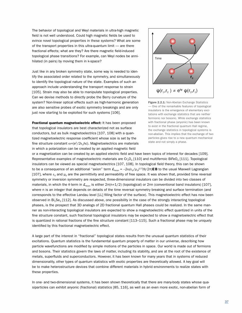
37
The behavior of topological and Weyl materials in ultra-high magnetic field is not well understood. Could high magnetic fields be used to evince novel topological properties in these systems? What are some of the transport properties in this ultra-quantum limit — are there fractional effects; what are they? Are there magnetic field-induced topological phase transitions? For example, can Weyl nodes be anni-hilated (in pairs) by moving them in k-space?
Just like in any broken symmetry state, some way is needed to iden-tify the associated order related to the symmetry, and simultaneously to identify the topological nature of the state. Examples of such an approach include understanding the transport response to strain [105]. Strain may also be able to manipulate topological properties. Can we devise methods to directly probe the Berry curvature of the system? Non-linear optical effects such as high-harmonic generation are also sensitive probes of exotic symmetry breakings and are only just now starting to be exploited for such systems [106].
Fractional quantum magnetoelectric effect: It has been proposed that topological insulators are best characterized not as surface conductors, but as bulk magnetoelectrics [107, 108] with a quan-tized magnetoelectric response coefficient whose size is set by the fine structure constant α=(e2/2ε0hc). Magnetoelectrics are materials in which a polarization can be created by an applied magnetic field or a magnetization can be created by an applied electric field and have been topics of interest for decades [109]. Representative examples of magnetoelectric materials are Cr2O3 [110] and multiferroic BiFeO3 [111]. Topological insulators can be viewed as special magnetoelectrics [107, 108]. In topological field theory, this can be shown to be a consequence of an additional “axion” term 𝓛Axion = –2α(ε0/μ0)1/2(θ/2π)E.B to the usual Maxwell Lagrangian [107], where ε0 and μ0 are the permittivity and permeability of free space. It was shown that, provided time reversal symmetry or inversion symmetry are respected, three-dimensional insulators can be divided into two classes of materials, in which the θ term in 𝓛Axion is either 2π(n+1/2) (topological) or 2πn (conventional band insulators) [107], where n is an integer that depends on details of the time reversal symmetry breaking and surface termination (and corresponds to the effective Landau level [LL] filling factor of the surface). This magnetoelectric effect has now been observed in Bi2Se3 [112]. As discussed above, one possibility in the case of the strongly interacting topological phases, is the prospect that 3D analogs of 2D fractional quantum Hall phases could be realized. In the same man-ner as non-interacting topological insulators are expected to show a magnetoelectric effect quantized in units of the fine structure constant, such fractional topological insulators may be expected to show a magnetoelectric effect that is quantized in rational fractions of the fine structure constant [113–115]. Such a fractional phase may be uniquely identified by this fractional magnetoelectric effect.
A large part of the interest in “fractional” topological states results from the unusual quantum statistics of their excitations. Quantum statistics is the fundamental quantum property of matter in our universe, describing how particle wavefunctions are modified by simple motions of the particles in space. Our world is made out of fermions and bosons. Their statistics govern the laws of matter, including its stability, and are at the root of the existence of metals, superfluids and superconductors. However, it has been known for many years that in systems of reduced dimensionality, other types of quantum statistics with exotic properties are theoretically allowed. A key goal will be to make heterostructure devices that combine different materials in hybrid environments to realize states with these properties.
In one- and two-dimensional systems, it has been shown theoretically that there are many-body states whose qua-siparticles can exhibit anyonic (fractional) statistics [85, 116], as well as an even more exotic, non-abelian form of
Figure 2.2.1: Non-Abelian Exchange Statistics — One of the remarkable features of topological insulators is the emergence of elementary exci-tations with exchange statistics that are neither fermionic nor bosonic. While exchange statistics with fractional phase (anyonic) has been known to exist in the fractional quantum Hall regime, the exchange statistics in topological systems is non-abelian. This implies that the exchange of two particles gives rise to a new quantum mechanical state and not simply a phase.
Time
ψ(r1,r2 ) ≠ eiφ ψ(r2,r1)
r1 r2
38
quantum exchange (Fig. 2.2.1). This type of quasiparticles is only possible in topological many-body states of matter with long-range quantum entanglement, of which non-abelian statistics is one of the most spectacular manifestations.
A remarkable feature of non-abelian quasiparticles is that the quantum state of several quasiparticles cannot be specified by their spatial locations (their coordinates). Instead, a set of non-abelian quasiparticles can be in several possible states [117]. Under a process known as braiding, the state of a collection of such quasiparticles can be turned into a superposition of several of the allowed states. It is this novel manifestation of quantum mechanics that renders systems with non-abelian quasiparticles extremely useful for building quantum information systems such as topologically-protected qubits and topological quantum computers [59, 118]. Just as a fermion cannot be turned into a boson, a (quasi) particle with non-abelian statistics has properties that are protected from disorder, local perturbations, and other local external factors [119]. The central goal of this line of research is to both find such topological phases of matter and to engineer novel, robust, extensive, and scalable platforms using topological and spintronics materials with the purpose of creating, isolating, manipulating and braiding novel excitations with esoteric quantum numbers and statistics. There are a number of promising avenues for research.
Non-abelian statistics and Majorana fermions: As originally proposed by Ettore Majorana, the Majorana fermion is a particle that is its own anti-particle. In the condensed matter context, of particular interest are Majorana fermion zero-modes arising at end-points (and surfaces) of odd-parity superconductors and at their junctions with conven-tional superconductors. The interest here is that topological singularities in vortices of p-wave superconductors and edge states of p-wave superconducting wires, harbor Majorana zero modes [62, 120]. As a consequence, these structures behave as non-abelian anyons (of the Ising type) and can serve as platforms for non-abelian braiding operations. In the condensed matter setting, Majorana fermion zero-modes can emerge in topological supercon-ductors as a special type of zero-energy, spatially-localized quasi-particle, formed by a coherent superposition of electron and hole excitations with equal amplitude [63]. Theory predicts that Majorana fermion zero-modes can be created in a wide array of spin-orbit-coupled materials in proximity to conventional superconductors [121]. These materials include, but are not limited to, topological insulators (2D or 3D), nanowires (semiconducting or metallic), and magnetic atom arrays. Recently, the observation of zero energy conductance peaks in these platforms provides encouraging hints of Majorana fermion zero-modes [122].
Condensed matter materials are made out of fermions and bosons and do not usually contain exotic quasiparticles. An exception has been the fractional quantum Hall effect. While for a long time it has seemed impossible to find a scalable way to manipulate non-abelian quasiparticles, recent remarkable advances have turned this from only a theoretical possibility into a probable 10-year reality. Rather than finding new, interacting materials in which the elec-trons reorganize themselves into states with new non-abelian quasiparticles, the recent experimental advances have focused on engineering these exotic phases using composite structures of different known materials. All the current platforms involve either proximity-induced superconductivity and nanowire semiconductors with spin-orbit coupling in the presence of a magnetic field, quantum spin Hall materials and proximity-induced superconductors [123, 124], or magnetic materials that form ferromagnetic chains via coupled “Shiba” states on the surface of superconducting lead [125]. In these engineered hybrid structures, these groups have seen the first glimpses of Majorana fermion zero-modes, which endow these structures with non-abelian statistics [125]. These successes have made the isola-tion, manipulation and braiding of the first exotic quasiparticle a possible, yet tremendously challenging, goal for the next 10 years. More excitingly, this goal can be, at least conceptually, achieved in platforms, which form a topolog-ical phase of matter out of simple, known materials. This allows for both lateral and vertical integration: laterally, these hybrid, engineered structures can be scaled up to eventually produce logical devices; vertically, they can be used to create platforms to manipulate and braid even more esoteric (but more robust) non-abelian quasiparticles of the future, such as the proposed parafermions [126].
Engineering states with parafermions and other exotic excitations: Hybrid structures using a generalized form of proximity effect between other phases of quantum matter may lead to exotic states. Recent theoretical results [127] suggest that hybrid structures of quantum spin-ice materials (a magnetic material in a spin liquid state lackinglong-range magnetic order) with a conventional superconductor results in a parity-odd (p-wave) superconductor at
39
its interface. In a different vein, it has been shown theoretically that a one-dimensional hybrid structure made of edge states of fractional quantum Hall systems and insulating density waves traps non-abelian quasiparticles known as parafermions [126], and potentially could be used to perform quantum computations. Clearly, the exploration of hybrid structures, carefully engineered, is a direction of research from which exciting new and potentially revolutionary discoveries may be made in the near future.
One of the major experimental challenges in exploring parafermions is the need to “proximitize” quantized Hall states with superconductivity at high magnetic fields. Presently there are several promising platforms that are believed to be able to do that. These include 2D systems made of graphene, InAs quantum wells, HgTe quantum wells, and even GaAs which holds the record in terms of cleanliness and was recently proximitized for the first time [128]. Another promising platform is the use of the quantum anomalous Hall system where coupling to quantum Hall physics can be done at zero magnetic field. Theoretically, Hamiltonian engineering in hybrid structures can also be used to create different types of parafermions that require symmetry protection [102]. These new types of sys-tems host quasiparticles, which are non-abelian, exotic, and protected by discrete symmetries. One specific simple example is the Z(8) Majorana phase [129], physically realizable in hybrid systems with mirror symmetry such as nanowires or atomic ferromagnetic chains on the surface of superconductors. The quasiparticle excitations of this state behave as a remarkable type of “spin” called projective representation. Scanning tunneling spectroscopy can in principle be used to image these quasiparticles.
A key outstanding problem is the characterization of topological phases of matter and in particular exploring their excitations. For topological superconductors, a direct test is provided by phase-sensitive measurements, which should provide direct evidence for the order parameter symmetry. Yet other more subtle probes are needed to fully characterize these states. For instance, time-reversal-breaking px+ipy superconducting states are predicted to have charge-neutral chiral edge states of Majorana fermions. To detect such states requires sophisticated techniques for measuring quantized heat transport. Such techniques have been employed in challenging experiments on the edge states of certain fractional quantum Hall systems [130, 131], but so far not in topological superconductors. Likewise new techniques are needed to image Majorana zero modes in topological superconductors, which will require further development of scanning magnetometry techniques and improvement of the resolution of quasiparti-cle tunneling spectroscopies adapted to these ends.
A first step in the development of functional topological devices is to identify the location of Majorana fermions in hybrid devices. Much of the evidence for Majorana fermions has come from the observation of zero-energy states in the conductance of tunneling contacts to topological semiconductor nanowires [122] and in chains of magnetic atoms [125] via STM and spectroscopy. The latter experiments allow imaging of the location and internal structure of the zero-voltage states. This technique can be applied to the search for Majorana bound states in Josephson junctions bound to Josephson vortex cores where the junction phase shift is 𝜋.
A key goal of future work is to develop new modes capable of locating and tracking Majorana fermions in topological systems. Possible approaches are a) charge imaging such as the scanning single electron microscope [132, 133], which is sensitive to the compressibility of the quantum modes and can probe buried interfaces, b) scanning mag-netic probes such as scanning nitrogen vacancy center microscopy, that are operable in a range of temperatures and magnetic fields and has single spin sensitivity, and c) magnetic resonance force microscopy and scanning SQUID microscopy, technologies that can be used to image vortices and magnetic states. Another powerful technique for testing the unusual statistics of Majorana states is vortex interferometry via the Aharonov-Casher effect, i.e., a peri-odic sensitivity of the vortex flux flow resistance of interfering vortex paths to the charge enclosed [123, 134]. Finally, an important step in detecting Majorana fermions is measuring the Majorana spin. This will depend on the platform used. In the nanowires, the magnetic chain platform, and the quantum spin Hall platform, the Majorana zero mode has significant smoking-gun spin signatures which can be measured in spin-dependent tunneling, possibly using spintronic devices.
Basic logical operations with Majorana fermions generally require exchanging them in space, which is the process of braiding. This requires moving the Majorana fermions. In networks of topological semiconductor nanowires, in

40
which the Majorana fermions are bound to the ends of the wires, this can be done by gating the wire into and out of the topological regime in T-junction structures. In networks of Josephson junctions, in which the Majorana states are bound to Josephson vortices, this can be done by moving the vortices by controlling the phase, current, or voltage across the junctions. Various logic gates can be realized by manipulating the Majorana and parafermion modes in different sequences. Likewise, quasiparticle interferometers that are sensitive to the fractional statistics, which have been used (so far with modest success) in fractional quantum Hall devices [135, 136], should be further developed. Of particular promise are devices that can test the behavior of a large assembly of Majorana and parafermion zero-modes. The theoretical studies of these setups have until now been very qualitative, and more predictive studies are needed to guide experiments.
Parity: Information is encoded in the parity of the Majorana fermion pairs. It is the non-local storage of this informa-tion that protects it against dephasing. The parity is a measure related to the charge of the pair when annihilated, or in Josephson junction devices to the sign of the sin(𝜙/2) component in the current-phase relation [137]. One of the major experimental challenges is to determine ways to readout the parity of Majorana states after braiding exchanges. Many schemes have been proposed: coupling of the Majorana states to a charge-sensitive quantum-dot, coupling them to a qubit, or reading the instantaneous critical current that is sensitive to the sign of the sin(𝜙/2) Josephson supercurrent. Achieving parity transitions in braiding operations would provide a direct test of the exis-tence of Majorana modes and their most important property, which is non-abelian statistics. It would also open the door to further development of electronic circuitry for topologically-protected quantum computing.
Although the braiding operations introduce no errors, the possibility of parity transitions induced by interactions with quasiparticle excitations will limit the operation of quantum computing. One of the major goals is to determine and reduce as much as possible the detrimental effects of quasiparticle excitations and enhance the parity lifetime. Measurement of the parity lifetime in Josephson junction systems can be determined by measuring the frequency- dependence of the Josephson current-phase relation: The sin(𝜙/2) component is averaged out by parity transitions. In nanowire systems, this can be estimated from the single-electron charging energy to the wire.
Topological Spintronics Devices: Another class of hybrid TI devices is those interfacing with ferromagnetic materials. New functionalities can be anticipated from the extreme spin-orbit coupling (spin-momentum locking) of topological surface states. For example, spin polarized current injection from a magnet into a TI should lead to an electrical cur-rent along a specific spatial direction in the TI, or, using the reciprocity of this effect, one can use spin-orbit torque from the TI to switch an adjacent ferromagnet. Similarly, because the pair of helical edge states that run along the edge of a two-dimensional TI circulates in opposite directions for electrons of opposite spins, it is easy to envision simple devices where these channels can be used. For example, the channels could be used to measure the polar-ization of an incoming current or to split a current into its polarization component. Channels might also be used to switch current on and off, or change the direction of change the direction of flow depending on polarization.
Research into spin injection has started only recently. It is challenging to convincingly demonstrate spin injection in TI materials. To obtain spin injection, several groups have attempted to use the spin torque technique to overcome the resistance mismatch between ferromagnet and TI, but clear evidence of spin current injected into a TI has yet to be provided. Simple dc spin injection and detection in a non-local geometry would be a very welcome demon-stration-of-principle, but it has so far proven very hard to obtain tunnel barriers of sufficient quality and in the right resistance range. Spin-orbit torque has been invoked to explain switching phenomena in a magnetic TI, but switching of an external magnet remains to be accomplished.

41
2.3 PRD 3 — DRIVE AND MANIPULATE QUANTUM EFFECTS (COHERENCE, ENTANGLEMENT) IN NANOSTRUCTURES FOR TRANSFORMATIVE TECHNOLOGIES
The most important and interesting processes in nature are heterogeneous and out of equilibrium, including by
necessity those behind our energy and technological systems. Under these conditions quantum materials have
distinct and unusual behaviors that present fundamental scientific challenges and unique opportunities for energy-
relevant technologies. The goal of this priority research direction is to explore the transport and non-equilibrium
properties of quantum matter and the properties of heterogeneous and finite size structures formed from quan-
tum materials. The Heisenberg uncertainty principle ensures that quantized energy levels shift as quantum
materials are truncated or confined. This effect can be utilized to shift the color of a light emitting diode or to
match the absorption of photovoltaics to the solar spectrum. Finite size effects are amplified and gain variety
when properties depend fundamentally on electron interactions. Confinement and defects can then extinguish or
enhance distinct materials properties because of symmetry breaking and anisotropic interactions at interfaces.
Another relevant feature of quantum materials is their frequently exotic quasi-particles, which, within the confines
of the material, are as real as electrons and photons are in vacuum. However, solid state quasiparticles —
phonons, magnons, spinons, visons, skyrmions, and magnetic monopoles, for example — have distinct collective
and transport properties that characterize the underlying quantum matter and can be exploited for applications
including information storage, transmission, and energy efficient processing based on electron spin rather than
charge. We perceive a tremendous potential for energy-relevant technological impacts that can be achieved by
understanding and controlling the unfamiliar properties of heterogeneous quantum systems far from equilibrium.
2.3.1 Introduction
Seventy years after the invention of the transistor, the average person now relies on more than 100 billion silicon- based transistors to conduct his or her energy and information intensive life. While the essential bulk characteristic of semiconducting silicon is chemical and electrical tunability, the technological impact is associated with nano- structuring of electronic functionality.
Compared with silicon, quantum materials offer a staggering variety of electronic properties: Collective phenomena give rise to extreme non-linear responses to stimuli, and ordered states host a variety of exotic quasi-particles that exhibit quantum coherence and entanglement properties from which, for example, the almost magical computational capabilities of quantum computing might be realized. As silicon-based information technologies approach physical limits set by dissipation, density, and speed, it is natural that we should look to this rich class of materials as a potential basis for an energy efficient extension of the information technology revolution.
As has been the case for silicon, nano-structuring of quantum materials will be key to their technological application and is a focus of this priority research direction. Beyond miniaturization, spatial confinement of quantum materials also presents the means to dramatically altering their physical properties, turning a metal to an insulator, a para-magnet to an antiferromagnet, or a magnet to a superconductor as required within a specific device. Using such tuning it may also be possible to drive a nanoscale volume of a quantum matter to a critical point that separates

42
such phases to greatly amplify the effects of stimuli. Assembling monolayers with controlled relative rotations and distinct chemical sequences, or interfacing layers of quantum materials with desired properties, offers a route to tailored electronic functionality in the nano-structured volume or at interfaces.
Whereas semiconductors host electrons and holes, quantum materials harbor an array of exotic quasi-particles that could form the basis for information storage, transport, and processing. A few such phases are exemplified in the subfield of magnetism. Skyrmions are compact topologically protected bubble-like textures that appear in ferro- or antiferro-magnetically ordered states and have well-defined dynamical properties. Magnons carry a quantum of magnetism that can be controlled and manipulated with high-energy efficiency. Spinons are topologically protected excitations of spin liquids with distinct quantum dynamics potentially applicable for quantum computation. Magnetic monopoles, the magnetic equivalent of electric charge, while not yet detected as fundamental particles in nature, have been realized as stable collective particles in a curious magnetic state of the pyrochlore crystal structure that mimics water ice. The exploration of generalized transport of these and many other collective quasi-particles in nano-structured quantum matter combines abundant opportunities for fundamental discovery with a realistic oppor-tunity to enable radical new low-power spin-based information storage and processing devices.
Stimulating quantum materials with femtosecond light pulses opens a new dimension in the space of quantum materials. Metastable states of matter that do not exist in equilibrium can be formed to achieve a specific electronic functionality at the designated time, desirable materials properties such as superconductivity can be enhanced by the coherent excitation of specific vibrational states (phonons), and magnetic bits in nanostructures can be indi-vidually switched with spatially patterned optical driving fields. Given that our fiber optic communication systems are based on pulses of light, the rich nature of interactions between light and quantum matter offers outstanding opportunities for fast and energy efficient transfer of information from optical encoding to assemblies of magnons, skyrmion, spinons, or monopoles for information processing within a quantum material.
Nano-structured quantum materials offer an exciting space within which to create a new class of ultra-fast comput-ing systems with seamless linkages to optical communication systems. Based on the spin rather than the charge of the electron, such systems also have the potential for a new level of energy efficiency. The application of advanced collective properties of quantum materials is shifting the traditional boundaries between fundamental and applied research. Thus the scientific challenges that we discussed in the next section, when overcome through work under this priority research direction, can have a rapid impact on applications. An excellent example is afforded by the phe-nomenon of giant magneto resistance (GMR), which is the basis for the modern hard disk. In the decade following the initial scientific discovery and before award of the corresponding 2007 Nobel Prize, 5 billion hard disks based on GMR read heads were already in service. Quantum materials offer extraordinary opportunities for groundbreaking technological progress to improve the energy efficiency and the performance of the information processing systems that are the basis for modern society.
2.3.2 Scientific Challenges
While traditional methods of condensed matter physics focus on the equilibrium properties of an infinite volume of homogeneous matter, a full understanding of quantum materials as they occur in nature and technology includes the exploration of finite size effects, surface effects, the effects of impurities, and the response to stimuli, large and small. Motivated by fundamental scientific curiosity or the practical interests of an application engineer, this focus complements and builds upon that of the two prior PRDs.
Extrapolation from the pristine crystalline bulk of a ‘simple’ material such as semiconducting silicon to realistic conditions is under excellent theoretical and experimental control. It is a different story, however, for quantum materials. Even in the bulk, predicting the superconducting or the magnetic transition temperature or the nature of the entangled state of a quantum magnet are significant challenges. Understanding collective properties under realistic conditions including finite sample sizes and finite defect densities is a profound challenge of fundamental and practical importance.

43
However, the concept of band engineering by assembling layers at the atomic scale either through molecular beam epitaxy or by stacking graphene-like atomic mono-layers as so-called moiré solids looks promising as a route to rational design of quantum matter.
An interesting aspect of quantum materials is their extreme sensitivity to specific small perturbations. Much like the extreme sensitivity of silicon to doping, once under experimental and theoretical control, such sensitivity can be of great importance in applications. For example illumination of Bi2Se3/SrTiO3 heterostructures can produce laterally patterned electronic surface states.
Because quantum materials harbor such a broad array of exotic quasi-particles, the study of the associated trans-port properties, namely the directed flow of quasi-particles within quantum materials in the bulk or in nano-struc-tured forms, is a rich area of science with close connections to applications. Spin currents might, for example, be employed to alter magnetic structures, and this might be a route to realizing neuromorphic computing, where the ability of brain cells to alter their connectivity is mimicked.
Another area of intense focus and promise is the application of antiferromagnetic materials for information storage and processing. There are multiple potential advantages including lower energy consumption, higher speed, and higher density. The information would be stored in domain structures that might be associated with states related to each other through mirror reflection. The scientific challenges that must be met to realize this vision are associated with understanding transport of quasi-particles through such magnetic structures and the associated domains, and this turns out to be an extraordinarily rich and exciting area of inquiry.
The skyrmion might be considered the ultimate atomic sized domain structure. In a range of magnetic solids with magnetic order and inversion symmetry breaking either within the bulk or as a consequence of an interface or a sur-face, these spin textures that resemble a rolled up hedgehog are remarkably stable once formed, and they may even form spontaneously. The physics of skyrmions, including their rich interactions with electrical currents, are again an area with profound intellectual challenges and tremendous potential for applications.
Moving beyond steady-state transport to conditions far from equilibrium, quantum materials present a plethora of surprising behaviors. Under the stimulation of intense pulsed lasers, it is possible to induce metastable phases, or states of matter that rely on the presence of large amplitude electromagnetic fields. Superconductivity can be strengthened by non-linear excitation of specific vibrational modes, which can both help to understand the origins of superconductivity and how to strengthen it in thermodynamic equilibrium and might serve as a means of switching quantum materials properties during the operation of an electronic device.
The focus on time-dependent non-equilibrium phenomena in the solid state developed from a different area of science, namely that of atomic, molecular, and optical (AMO) physics, where such effects are used to manipulate and probe ultra-cold atomic gases. An exciting marriage of several of these concepts is relevant to the electronic and nuclear spin dynamics of the nitrogen-vacancy (NV) defects in diamonds. The relatively long quantum coherence times of these systems along with the ability to manipulate their quantum entanglement through interactions with photons makes NV systems an exciting area of fundamental inquiry, as well as a potential arena for storing, replicat-ing, and processing quantum information.
2.3.3 Research Thrusts
The PRD is organized into three main “thrusts” that progressively deviate from homogeneous equilibrium condi-tions. The first thrust deals with spatially non-uniform quantum materials. At the atomic scale materials always come in atomic chunks, but here we consider structure on longer length scales from nanometers to fractions of a millimeter (Thrust 3a). In the second thrust (Thrust 3b) such structures are subject to boundary conditions that lead to a flow of energy, charge, and spin and of the unique quasi-particles that define the quantum material. In the third thrust (Thrust 3c) we consider quantum materials far from equilibrium as they are stimulated by intense

44
electromagnetic pulses and form strongly interacting systems of photons and matter so that the focus becomes the time evolution of interacting quantum systems.
Thrust 3a: Employ Nanoscale Structuring to Elucidate and Exploit Coherence and Entanglement
The 20th century technology revolution in electronic, photonic, and magnetic materials was enabled by extraordinary control over the properties of materials for which a theoretical framework with near-perfect predictive capabilities was already in place. In contrast, the scientific understanding of how to control the unique phenomena exhibited by quantum materials, which arise from strong electron correlations and non-trivial topological electronic states, is still in its infancy, and studies have largely been limited to bulk materials. The premise of this thrust is the realization that nano- and heterostructures allow for new ways of controlling and understanding the phenomena exhibited by quantum materials and for creating new quantum states that do not exist in higher dimensions. The key approaches of this thrust include control of dimensionality through electrostatic confinement, layer-by-layer thin film growth meth-ods, and nanopatterning; control of carrier densities through field effect, modulation doping, or the use of polar/non-polar interfaces; orbital control and exploitation of proximity effects at interfaces and in hybrid structures; and band engineering in van-der-Waals heterostructures. Key outcomes include (i) understanding how to systematically utilize scaled and heterostructured quantum materials to enhance existing properties and realize new physical behavior and (ii) highly tunable structures that provide strong constraints on the theoretical models, leading to the long-sought predictive models for these materials. Ultimately, such highly scaled quantum materials will enable entirely new classes of energy-efficient, spintronic, and electronic materials that utilize the wealth of phenomena associated with strong electron correlations, topological energy states, and spin-orbit coupling.
Scientific objective: The scientific objective of this thrust is the rational design of quantum materials and control over their properties by exploiting quantum confinement and low dimensionality at heterointerfaces and in nanoscale geometries. A major challenge one encounters in quantum materials lies in the cooperation and competition of key variables, such as dimensionality, spin, charge, collective modes, order parameter symmetry and fluctuations, and lattice degrees of freedom, all of which are crucial in promoting new emergent states (Fig. 2.3.1). In bulk materials, it is, however, very difficult to access and control these key variables independently. For example, low-dimensionality can promote new states by breaking inversion symmetry or suppressing other electronic and magnetic instabilities. Structural deformations (Fig. 2.3.2), which control the electronic and orbital degrees of freedom, typically cannot be systematically tuned in bulk materials without altering material chemistry. This complicates theoretical understand-ing of the underlying electronic phenomena and the rational design of new correlated quantum matter. Scaled quan-tum materials offer a different way of controlling structural deformations via confinement, orientation, and strain, which provides unique opportunities to develop a quantitative understanding of the interplay between electronic correlations and structure.
Ordering phenomena• Magnetic• Charge• Orbital
Fluctuations in charge, orbital, and spin
Spin wave excitations(magnons)
Phenomena
Correlated 2D Electron System
Correlated electron transport• Anomalous
magnetotransport• Mass enhancement• Non-Fermi liquids• Bad metals• Coupling to phonons,
plasmons, and excitons, localization
• Localization• Metal-insulator
transitions
Bandwidth
Filling Orbital degeneracy
“U”
Spin exchange
Superconductivity
Dimensionality
Figure 2.3.1: Tuning parameters afforded in heterostructures of highly scaled correlated materials and the phenomena that they control.

45
Highly scaled, heterostructured quantum materials allow for important parameters to be independently controlled in ways that have barely been explored. For example, carrier densities can be manipulated without chemical doping in the active volume through the field effect, modulation doping, or the use of polar/non-polar interfaces. The dimen-sionality of the electron system and that of the critical fluctuations can, in principle, be controlled through elec-trostatic confinement and layer-by-layer control afforded by modern thin film synthesis techniques. In many cases, however, high-quality thin film synthesis is proving to be a significant challenge in its own right, due to the inherent complexity of the materials. Proximity effects at interfaces can be used to introduce specific types of magnetism, to control orbital polarization, and to alter unit cell symmetry. Heterostructures and field effect devices caused a para-digm shift in conventional semiconductors, and no less is expected in the arena of correlated and complex quantum matter, topological materials, and 2D crystals.
The thrust is to develop and exploit nano-structuring as a means of controlling relevant parameters of quantum materials systems — including quantum fluctuations, lattice symmetry, orbital polarization, and magnetic or orbital order — and their interplay so as to understand and form new states of matter.
Three research challenges are central to rational design of highly scaled quantum matter:
• How can we tune the “character” of individual electronic states in quantum materials? Correlated electronic materials display great sensitivity to the type and shape of electronic orbitals and to the associated bandwidths, all of which are impacted by nano-structuring.
• How can we tune the number of electrons in a solid? Nano-structuring allows for electrostatic gat-ing that can alter the electronic landscape of quantum materials without introducing disorder and lattice distortions. Due to the short screening length in oxides, atomically thin layers are ideal for manipulating the local effects caused by carrier injection and/or depletion on exchange, orbital, and lattice interactions. In this way quantum criticality may be accessed through gating. In 2D van der Waals materials, the carrier density can also be modulated along the vertical growth direction using adjustable band alignments at heterointerfaces and by exploiting the relative twist degree of freedom between layers. The large thickness dependence of the electronic band structure of these 2D materials also lends itself to lateral modulation of carrier density.
• How can we tune electronic interactions? Approaches include dimensionality control, which is closely tied to the first approach, since orbital states are highly sensitive to the dimensionality. With the
Figure 2.3.2: Schematic showing the control of orbital polarization in octahedrally coordinated LaNiO3 or manganites, using strain and confinement. The top row shows the structural deformations and the bottom row the relative occupancy of the d-orbitals. The actual (experimentally measured) changes in the orbital polarization are on order of tens of percent or less.
Tensile strain Compressive strain Connement
3z2-r2
x2-y2
3z2-r2
x2-y2
3z2-r2
x2-y2
46
advent of high-quality quantum materials heterostructures, dimensionality can be tuned with methods such as atomic layer control and electrostatic confinement. Other approaches include band engineer-ing in 2D heterostructures, interfacial spin-orbit coupling, and the use of interfacial polarity. Band engineering extends a methodology that is well established in semiconductor heterostructures, but that is much more powerful within the context of 2D van der Waals materials. Here, stacking diverse monolayers gives access to a much larger phase space of band structures.
Characterization of such engineered materials and structures is now possible through new spectroscopic and micro-scopic techniques that reveal electronic and lattice configurations on sub-nanometer length scales (see 3.6.2). At the level of synthesis, unprecedented control of samples is possible through thin film growth techniques, such as molecular beam epitaxy (MBE), and 2D synthesis techniques that allow atomic precision design of layered struc-tures (see 3.6.1).
Tuning the “character” of individual electrons in quantum materials: The phenomena exhibited by correlated materials depend sensitively on the atomic orbitals from which the electronic structure is derived. Important orbital characteristics include directionality, polarization, and quantum nature. Orbital overlap, controlled by subtle structural distortions, determines the electronic kinetic energy, which in turn determines phenomena such as hopping param-eters, metal-insulator transitions, and exchange interactions. Relativistic spin-orbit coupling can induce intrinsically complex orbital wave functions, which lead to pronounced quantum effects such as the accumulation of phase as electrons move through the solid. In correlated magnetic materials, the interactions between individual moments determine their antiferromagnetic or ferromagnetic character while anisotropy is controlled by the orbital configura-tions. Tremendous excitement was generated when it was appreciated that manipulation of such factors in hetero-structures may allow for the design of unconventional superconductors [139, 140].
While the orbital configuration of quantum materials are essential for functions, options to manipulate this configura-tions without changing crystal structure and/or composition are severely limited in conventional bulk synthesis. For example, in rare earth nickelates the crystal symmetry, orbital degeneracy, and bandwidth, which control the metal insulator transition, are controlled by the rare earth ion on the perovskite A-site. Using thin film techniques, where the atomic layers can be deposited precisely in a wide range of geometries, subtle perturbations can be introduced through interfacial symmetry, coupling, and coherency strains, so the orbital polarization can be explicitly controlled. One approach involves combining layers of different thickness and with different rigidity. Interface coherency then causes the lattice of sufficiently thin, electronically active layers to be effectively frozen, to suppress or enhance distortions and thus stabilize a desired orbital configuration. Because the spin interactions are heavily influenced by the preferred orbital orientations, new spin and depth-dependent orbital textures may arise in these systems. Another potential approach to controlling the orbital state of quantum materials involves the use of electromagnetic radiation, which can directly influence electronic parameters.
Tuning the number of electrons in a single solid: Like their conventional semiconductor counterparts, scaled quantum heterostructures allow for control of the electronic carrier densities. Strong electron correlations start to dominate phenomena in quantum materials only at very high electron densities, in narrow bands, and for sufficiently strong electron Coulomb repulsion energies. The extreme case is the Mott insulator. More interestingly, however, rapid changes of the physical properties occur as the electron density is “doped” away from the Mott insulating state. Some of the most exotic — and least understood — phenomena in condensed matter physics occur in the proximity of this Mott insulating state, such as high-temperature superconductivity, metal-insulator transitions, pseudogap phenomena, charge ordering, and tunable magnetism. In many of the most interesting systems, carrier density tunes the materials across quantum phase transitions that may promote new exotic states of matter [141]. Control of carrier density may also enable the realization of entirely new states in correlated quantum materials. For example, it may be possible to realize quantum spin liquids by doping low-dimensional, quantum antiferromag-netic insulators.
In bulk materials, chemical doping (sometimes better described as alloying) is the only way to manipulate equilib-rium carrier densities. This method, however, introduces disorder, lattice distortions, and sometimes even nanoscale
47
inhomogeneities that are very difficult to detect. Furthermore, since the material is fundamentally altered, it can-not be tuned in situ, as would be needed for devices that utilize the change in properties that occur as the carrier density is tuned. Scaled quantum materials allow going beyond the alloying paradigm by using techniques that have been highly successful in semiconductor technology, such as modulation doping and electrical gating. Electrostatic doping can thus provide a well-defined route to exotic conducting and superconducting states of matter.
A major challenge is that large carrier densities need to be modulated (on the order of 1×1014 cm–2 [142]), which, in conventional field effect devices is limited by permittivity of the gate dielectric. Fortunately, within the family of perovskite oxides, several high permittivity oxides exist, though they often come with their own challenges, such as field-dependent dielectric constants. Innovative heterostructure approaches may be needed, but these have barely been explored, often due to the lack of very basic information, such as band offsets. Electrolytic “gating,” whereby a bias is used to induce large changes in carrier concentration and bonding environment through either electrostatic or electrochemical processes, provides a route to significantly alter electronic and magnetic behavior. In oxides, for example, the ability to dynamically insert and remove oxygen through external stimuli [143] can provide a means to reversibly traverse phase boundaries between different electronic and magnetic states in a single sample.
In van der Waals heterostructures that combine different 2D materials, the unpinned band alignment at heterointer-faces provides another powerful “control knob” for the carrier density. This knob can be controlled using either an externally applied electric field or by exploiting the ability to change the twist angle between alternating 2D layers in a stack. Such flexible control over the charge density distribution could have profound influence on properties such as magnetic order, superconductivity, and metal-insulator transitions. How will these phenomena develop in the presence of further quantum confinement such as in nanowire or quantum dot geometries? This remains an open question, full of exciting possibilities that have yet to be explored.
Surface adsorbates (i.e., alkali metals, such as K or Cs) provide an alternate route to carrier doping of atomically thin materials or the surface layers of quantum materials. One advantage to surface adsorbates is the high carrier densities (1014 cm2) that are achievable at the surfaces of materials [144], which can even exceed the density possible by ionic liquid gating. This could also provide a promising alternate pathway to doping materials where chemical substitution results in trapped states or chemical disorder. This approach has already been successfully employed to dope monolayer van der Waals materials, and it could also help in the search for more exotic states of matter. For example, there are indications that superconductivity can be induced at the surface of Sr2IrO4 with K adsorbed on the surface [144]. In contrast, La-substitution for Sr instead results in carrier localization and no hints of superconductivity.
Interfacing oxides with 2D van der Waals materials remains a relatively unexplored area with several recent discov-eries that are still incompletely understood. For instance an anomaly in resistivity measurements for a single layer of FeSe on SrTiO3 was reported and interpreted as indicative of superconductivity at a surprisingly high temperature [145,146]. Another discovery is that illumination of Bi2Se3/SrTiO3 heterostructures can lead to a laterally patterned chemical potential in the surface states of the Bi2Se3 and optical patterning of magnetic domains in Cr-doped (Bi,Sb)2Te3 [147]. Phenomena such as these are dependent on the complex charge transfer that occurs at highly heterogeneous interfaces.
Tuning interactions: Reduced dimensionality has long been known to promote new phases and new states of matter. Quantum confinement effects are generally important when the characteristic energy associated with confinement dominates. Given that a defining feature of correlated matter is competition between energy scales, confinement can be used to disentangle competing degrees of freedom. This is again an idea that remains to be explored. Low-dimensionality enhances quantum and thermal fluctuations, the thermodynamic density of states, and the phase space available for electronic scattering. The degree to which these play a role in high-temperature superconductivity and quantum criticality remains a matter of scientific debate. In particular, quasi-2D and 1D have been invoked in extensively studied systems, such as the cuprate and Fe-based superconductors and in organics. In bulk materials, reduced dimensionality usually occurs serendipitously and can be controlled only to a certain degree. For example, it is well known that in the layered Ruddlesden-Popper structures of correlated oxides, the ground state
48
can be changed dramatically as a function of the number of rock salt layers per unit cell. In the manganites and nickelates, the ground state can change from a ferromagnetic metal to an insulating state with nanoscale charge/spin ordering. Engineered, atomically thin analogs of these materials could allow for more precise tuning between such competing states, or even the realization of additional phases that are not possible in bulk form.
Electronic dimensionality may be different for different degrees of freedom (spin, charge, and lattice). In real material systems, there is a host of other effects that influence electronic correlations. An example is when the surfaces of a thin film break inversion symmetry. This breaking of symmetry in turn leads to Rashba spin-orbit coupling. In the absence of strong electronic correlations, the spin-orbit coupling can lead to spin-split states at the Fermi energy in an electron gas, and this can in some circumstances favor unconventional pairing of electrons in a superconducting state at low temperatures. On the other hand, if strong correlations are present, a magnetic insulating state may be formed. Spin-orbit coupling generically produces anisotropic interactions in a local moment model, which in turn typically favor non-collinear magnetic orders. Since the strength of the Rashba spin-orbit coupling decreases with distance from the surface of the film, the anisotropic components of the interactions in a local moment model are strongest at the interface. Hence, one may, in general, expect interesting “depth-dependent” spin textures. In the extreme ultrathin limit, where the two surfaces of the film have coalesced into a single layer material, quantum confinement effects are maximized, and the system is electronically two-dimensional. Such systems are ideal for understanding quantum materials, allowing one to experimentally investigate disorder, doping, magnetic impurities, and subtle correlations effects, such as abelian versus non-abelian excitations — the latter being forbidden in three-dimensional systems. As many experiments have indicated, the substrate supporting such films can play a vital role in the physical properties of the combined substrate/film system, so there is a need for theoretical work that considers such details.
Band engineering through vertical modulation of composition is a well-established methodology that has been effec-tively exploited in semiconductor opto-electronics. However, in conventional semiconductors, epitaxial growth is con-strained by the need for lattice-matching to avoid the creation of crystalline defects such as misfit dislocations. The 2D van der Waals materials avoid this constraint because of van der Waals bonding, and this offers a broader pal-ette of building blocks within heterostructures. An excellent example is provided by transition metal dichalcogenide monolayers: Materials such as MoS2 are indirect band gap semiconductors in the bulk, but the band structure is that of a direct band gap semiconductor at the single monolayer level [148]. Although adding a single additional layer immediately reintroduces the indirect band gap, first principles calculations indicate that the direct gap of the monolayer might be sustained in thicker heterostructures assembled from different 2D materials. For instance, bilayer stacks such as WS2-MoS2 and WSe2-MoSe2 are predicted to retain a direct band gap with a value ranging from ~0.8 eV to ~1.16 eV, depending on the bilayer materials [149]. Band engineering using 2D building blocks such as these has enormous scientific and technological potential. We can envision designing band structures that yield highly efficient light emitters at wavelengths of optoelectronic interest, resonant tunneling diode structures with high contrast negative differential resistance, and spintronic or valleytronic devices that take advantage of tailored spin-orbit coupling [150]. Further reduction in dimensionality is possible in nanowire and quantum dot geometries, which are only just beginning to be explored in this context. The effects of such extreme quantum confinement in materials such as the TMDs with record exciton binding energies are likely to result in new discoveries that stem from quantum phenomena such as Bose condensation of strongly confined quasiparticles.
Energy-relevant technological impacts: A key challenge in contemporary materials physics is the identification of new electronic materials that can reduce power consumption in information processors, since this currently limits the performance of CMOS-based computer chips and memories. This would also help to reduce energy consumption of the power-hungry computer systems that shape every aspect of quotidian life. Hetero- and nano-structured quan-tum materials could play an important role here: In contrast to the materials in existing electronic circuits, which have a relatively simple unified description, correlated electron systems display a panoply of unique phenomena including diverse types of magnetism, metal-insulator transitions, and long-range quantum entanglement. A com-mon characteristic is the interplay between interactions that are weak in conventional electronic materials, such as electron-electron interactions and the relativistic spin-orbit coupling. Closely competing states of matter that arise from these interactions are particularly interesting because external stimuli, such as electric or magnetic fields, can
49
drive transitions between phases with vastly different properties (for instance, magnetic to non-magnetic or metal-lic to insulating). We can imagine exploiting such state changes in hetero- and nano-structured correlated electron materials as the basis for new computing platforms or information storage systems. Skyrmion states of chiral metal-lic ferromagnets are currently being intensely studied for possible high-density storage applications. The intrinsic size of the skyrmion “bit” is limited by weak Dzyaloshinskii-Moriya interactions in currently studied materials, but could be reduced by an order of magnitude or more by using doped Mott insulators where the skyrmion size is set by frustrated exchange interactions. An interesting question worth addressing is whether one can design correlated electron nano- and hetero-structures that would allow control over the scale and motion of skyrmions. Spintronics is already contributing to energy efficiency in information technology. Recent research has established that antifer-romagnetic metals and insulators can be manipulated electrically by exploiting spin-orbit interactions. In spintronic technology, antiferromagnets have minimal stray fields, immunity to external magnetic field, and fast dynamics. Their technological application could have a transformative impact.
2D van der Waals materials create new opportunities for potential energy efficient technologies through their unique properties. For instance, the recently discovered valley Hall effect [151], resulting from the interplay between spin and valley degrees of freedom, allows the steering of spin-polarized charge carriers via electric fields, which enables qualitatively new, perhaps more energy efficient, information processing platforms based upon “valleytronics.” The spin-orbit coupling in 2D van der Waals materials is just starting to be explored within the context of spin-transfer torque devices. Reports of highly efficient spin-charge conversion in the 2D surface states of chalcogenides [152] suggest extensions to tailored 2D van der Waals devices that form the basis of energy efficient spin-transfer torque devices. Finally, many of the 2D van der Waals chalcogenides are already excellent thermoelectrics. Understanding how to optimize their thermoelectric figure-of-merit by tailoring their quantum properties could have very important implications for energy applications.
More futuristic applications of correlated and 2D van der Waals materials in nano-structured geometries can also be envisioned: Can we harness the quantum computing promise of entangled electron spins in a spin liquid stabilized within a 2D realization of a 3D harmonic honeycomb iridate? Can we optimize and apply high-temperature supercon-ductivity in Fe-chalcogenide monolayers?
Thrust 3b: Understand Transport in Quantum Materials
Transport refers to the flow of charge, spin, or energy, or sometimes other more exotic degrees of freedom, in response to voltage biases, thermal gradients, electromagnetic fields, or other less common stimuli. Measurements of transport properties are ubiquitous; for example, the basic transistor operation is such a measurement. The transport properties of quantum materials sometimes reflect novel physics that is inherently interesting, and some-times provide a wealth of information about underlying quantum states that is complementary to that provided by other properties. Transport measurements play a key role in materials discovery: Routine DC measurements are often the first characterization method applied to any conducting, superconducting, or semiconducting material. The importance of transport in studies of quantum materials is reflected by the fact that 14 Nobel prizes have been awarded to experiments related to transport phenomena. More are likely to be awarded in the future.
This thrust identifies two important broad areas where transport promises to unravel new phenomena, create new knowledge, and enable new technology.
Spin Transport and Dynamics: the Science of Spintronics: Spintronics has seen an explosion of new ideas in recent years, and is poised to make even greater advances in the next five to 10 years by leveraging progress in heterostructure design, exploiting new bulk materials, using advanced characterization techniques, and advancing theoretical understanding of charge and spin transport in different types of quantum materials. The science of spin transport in solid materials was once fundamentally coupled to the science of charge transport, because electrons carry spin as well as charge when they move. In quantum materials, this concept breaks down because charge and spin often move independently. Unlocking spin from charge leads to a wide range of new magnetic and mag-neto-transport phenomena that have not yet been thoroughly explored or exploited. Research activity following the threads described below looks particularly promising.

50
Spintronics combines abundant opportunities for fundamental discovery with a realistic opportunity to enable new lower power spin-based information storage and processing devices. This field of research explores how spin cur-rents can be created, how they are affected by magnetic structure, and how they can be used to control magnetic states. In its initial stages, spintronics focused mainly on generating and detecting spin-polarized currents by pass-ing charge currents through ferromagnetically ordered metals. The recent discovery that non-magnetic materials with strong spin-orbit coupling provide an efficient means of creating and detecting large spin currents was a surprise. The science underlying this effect, often described in terms of spin-orbit-interaction generated torques and explained in terms of bulk spin Hall or surface Rashba effects, is currently debated. But the main point is already clear: The transfer of spin across an interface does not require charge transport across that interface.
Discoveries in spintronics have in the past transitioned remarkably quickly into applied technologies. It appears that many more recent fundamental discoveries are now poised to have significant applied impact. Harnessing spin-orbit effects, in particular, provides a novel avenue for efficient manipulation of magnetization, especially at the nanoscale. For example, spin-orbit torques open up new strategies to exploit and understand spin transport in both ferromagnetic and antiferromagnetic insulators, many of which have exceptionally weakly damped collective dynamics. They might also provide a new means to study insulating materials with poorly ordered or even disordered quantum spins, and open up the possibility of systematic studies of spin superfluidity. Spin-orbit induced trans-verse spin currents are also very efficient at manipulating and creating topological magnetic solitons, such as chiral domain walls and skyrmions, and provide a way to control and generate magnons and possibly also a pathway for the electrical generation of Bose-Einstein condensates of magnons.
The importance of spin-orbit coupling has motivated the addition of new types of materials to the spintronics palette including topological insulators, antiferromagnetic metals and insulators, ferromagnetic insulators, and 2D materials such as single-layer transition metal dichalcogenides. New heterostructures, which break inversion symmetry and therefore enhance spin-orbit interactions, are especially important.
Transport in 2D materials: Layered van der Waals structures have opened up a new frontier in materials science and in the transport physics of quantum materials. Examples of opportunities include the possibility of constructing new low-power devices based on dissipationless spin or Cooper pair or electron-hole pair conduction at room tem-perature. The materials of interest include metals, semiconductors, insulators, and semimetals including hexagonal boron nitride, graphene, and transition metal dichalcogenides. As an illustration of the new physics that needs to be explored we highlight two important recent issues: physics that exploits the valley degree of freedom in transition metal dichalcogenides giving rise to a class of transport phenomena known as valleytronics, and transport physics related to the moiré patterns formed by graphene on a hexagonal boron nitride substrate.
Spin-orbit torques: When electrons travel through solid-state materials that incorporate heavy elements, the electric fields from these heavy element atoms generate a magnetic field in the rest frame of the traveling electron that couples directly to their magnetic spin degree of freedom. This interaction is known as spin-orbit coupling and is at the heart of many contemporary research topics related to spin transport. When inversion symmetry is broken at interfaces, this spin-orbit coupling can be further enhanced due to associated electric fields, a phenomenon known as Rashba spin-orbit coupling. These spin-orbit coupling effects make it possible to convert electric charge currents into spin currents and to electrically induce net spin accumulations. Topological insulators provide an extreme example in which the strongly spin-orbit coupled metallic conducting states that exist on the surfaces of these mate-rials have strong locking between the direction of an electron’s motion and its spin direction. Importantly, the spin currents and spin accumulations originating from spin-orbit coupling can interact with ordered magnetic moments and generate torques, known as spin-orbit torques. Spin-orbit torques are surprisingly efficient for magnetization direction switching and generation of magnetization dynamics.
The fact that electric current generated spin accumulations can exert torques on ordered magnetic structures has been realized for more than two decades. The spin accumulations were initially generated by passing an electric current through a ferromagnetic conductor. This mechanism can supply at most one quantum of electron spin per electron in the charge current. By using spin-orbit torques, however, the ratio between spin and charge currents can
51
be arbitrarily large because each charge carrier can transfer spin to the ordered magnetization multiple times. The spin-orbit torque mechanism therefore enables extremely efficient manipulation of magnetization. Moreover, the transfer of spin does not require actual charge transport across the same interface because transverse spin trans-port phenomena can be used. This property means that spin-orbit torques can be used to manipulate magnetization even in insulators, where magnetization dynamics can have exceptionally low damping. For low-damping magnetic materials, where non-linear interactions become important, it has even been shown that spin-orbit torque driven magnetization dynamics may give rise to dynamical solitons. Concomitantly, it has been realized that spin-orbit torques are very efficient at manipulating topological solitons in spin textures, such as domain walls and skyrmions, and can even provide novel pathways for their generation.
So far spin Hall effects have been investigated only in a very limited range of materials. Starting from the pioneering work detecting weak spin Hall effects in semiconductors in the early 1970s, the field exploded with the discovery during the last decade that spin Hall effects in metallic materials can result in practically useful spin torques. Nevertheless, research has so far focused mostly on elemental metals and some dilute binary alloys. A wide range of materials are ripe for exploration, especially since it has been shown that sizeable spin transfer torques can also be generated from spin Hall effects in magnetically ordered materials, including antiferromagnets. In addition, it has been shown that spin-orbit torques can even be important in the material that generates them, and can give rise to magnetization dynamics and switching, again even in antiferromagnets, where the torques can have the same stag-gered symmetry as the magnetic order. Lastly, as mentioned above the additional symmetry breaking associated with 2D materials can give rise to enhanced spin-orbit coupling, and thus offer new opportunities for extremely large spin-orbit torques. These 2D systems include the surface states associated with topological insulators, as well as physically 2D systems, such as graphene-like monolayers of dichalcogenides, which can also have sizeable spin-or-bit coupling due to the incorporation of heavy elements, such as Mo and W.
The generation, control, and detection of pure spin currents is a scientifically rich topic that offers a range of tech-nological opportunities. Precessing ferromagnetic magnetization emits spin currents (a phenomenon known as spin pumping) [153, 154]; conversely spin currents applied to FMs exert torques that can reduce magnetization damping, to the point of driving magnetization precession and reversal [155-157]. These phenomena have applications to high frequency signal generation and detection, and to efficient writing of nanoscale magnetic memory elements. They offer the prospect of using nanomagnets as amplifiers for weak magnetic signals. Recent developments suggest the possibility of in operando tuning of spin currents from spin wave modes defined by the localized dipole field of a scanned micromagnetic probe [158]. This offers a new horizon for controlled generation and manipulation of localized spin currents and scannable localized sources of microwave fields and spin currents. Antiferromagnets are attractive for spin-based functionality because they offer much higher intrinsic frequencies (THz vs GHz) and are much less sensitive to stray magnetic fields. This has motivated study of AFs for spin current-based applications. It was recently shown that insertion of thin AF films can enhance spin currents emitted by FMs into normal metals and that AFs exhibit relatively long decay lengths [159], suggesting these could offer a promising avenue for discovery of new spin current phenomena and applications.
The very efficient means of magnetization manipulation provided by spin-orbit torques is already pursued in modern information technologies, where the non-volatility of magnetic materials reduces the need for stand-by power. Along similar lines, spin-orbit torques may enable fatigue free memristors, which could be key to neuromorphic computational architectures. But beyond this, spin-orbit torques are a key ingredient in application schemes harnessing magnetic exci-tations in insulating materials, with transformational potential for energy efficient electronics. Using the wave-nature of long-lived magnetic excitations may furthermore enable approaches reminiscent of quantum computation.
Beyond the near- and far-term applications of spin-orbit torques for highly efficient data storage and processing, their Onsager reciprocal effects where charge currents are generated from spin currents or spin-dynamics provide a strategy for energy conversion at the nanoscale, because they enable the transformation of both heat currents and mechanical orbital motion into charge voltages and currents. Because of this ability, they may enable new energy scavenging applications where excess energy is locally harvested from continuously renewable energy sources, such as mechanical vibrations or thermal energy.
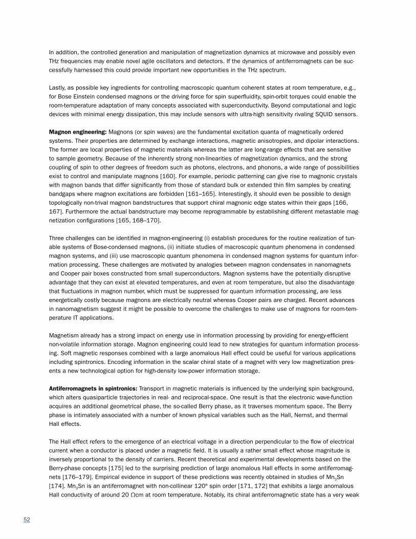
52
In addition, the controlled generation and manipulation of magnetization dynamics at microwave and possibly even THz frequencies may enable novel agile oscillators and detectors. If the dynamics of antiferromagnets can be suc-cessfully harnessed this could provide important new opportunities in the THz spectrum.
Lastly, as possible key ingredients for controlling macroscopic quantum coherent states at room temperature, e.g., for Bose Einstein condensed magnons or the driving force for spin superfluidity, spin-orbit torques could enable the room-temperature adaptation of many concepts associated with superconductivity. Beyond computational and logic devices with minimal energy dissipation, this may include sensors with ultra-high sensitivity rivaling SQUID sensors.
Magnon engineering: Magnons (or spin waves) are the fundamental excitation quanta of magnetically ordered systems. Their properties are determined by exchange interactions, magnetic anisotropies, and dipolar interactions. The former are local properties of magnetic materials whereas the latter are long-range effects that are sensitive to sample geometry. Because of the inherently strong non-linearities of magnetization dynamics, and the strong coupling of spin to other degrees of freedom such as photons, electrons, and phonons, a wide range of possibilities exist to control and manipulate magnons [160]. For example, periodic patterning can give rise to magnonic crystals with magnon bands that differ significantly from those of standard bulk or extended thin film samples by creating bandgaps where magnon excitations are forbidden [161–165]. Interestingly, it should even be possible to design topologically non-trival magnon bandstructures that support chiral magnonic edge states within their gaps [166, 167]. Furthermore the actual bandstructure may become reprogrammable by establishing different metastable mag-netization configurations [165, 168–170].
Three challenges can be identified in magnon-engineering (i) establish procedures for the routine realization of tun-able systems of Bose-condensed magnons, (ii) initiate studies of macroscopic quantum phenomena in condensed magnon systems, and (iii) use macroscopic quantum phenomena in condensed magnon systems for quantum infor-mation processing. These challenges are motivated by analogies between magnon condensates in nanomagnets and Cooper pair boxes constructed from small superconductors. Magnon systems have the potentially disruptive advantage that they can exist at elevated temperatures, and even at room temperature, but also the disadvantage that fluctuations in magnon number, which must be suppressed for quantum information processing, are less energetically costly because magnons are electrically neutral whereas Cooper pairs are charged. Recent advances in nanomagnetism suggest it might be possible to overcome the challenges to make use of magnons for room-tem-perature IT applications.
Magnetism already has a strong impact on energy use in information processing by providing for energy-efficient non-volatile information storage. Magnon engineering could lead to new strategies for quantum information process-ing. Soft magnetic responses combined with a large anomalous Hall effect could be useful for various applications including spintronics. Encoding information in the scalar chiral state of a magnet with very low magnetization pres-ents a new technological option for high-density low-power information storage.
Antiferromagnets in spintronics: Transport in magnetic materials is influenced by the underlying spin background, which alters quasiparticle trajectories in real- and reciprocal-space. One result is that the electronic wave-function acquires an additional geometrical phase, the so-called Berry phase, as it traverses momentum space. The Berry phase is intimately associated with a number of known physical variables such as the Hall, Nernst, and thermal Hall effects.
The Hall effect refers to the emergence of an electrical voltage in a direction perpendicular to the flow of electrical current when a conductor is placed under a magnetic field. It is usually a rather small effect whose magnitude is inversely proportional to the density of carriers. Recent theoretical and experimental developments based on the Berry-phase concepts [175] led to the surprising prediction of large anomalous Hall effects in some antiferromag-nets [176–179]. Empirical evidence in support of these predictions was recently obtained in studies of Mn3Sn [174]. Mn3Sn is an antiferromagnet with non-collinear 120º spin order [171, 172] that exhibits a large anomalous Hall conductivity of around 20 Ωcm at room temperature. Notably, its chiral antiferromagnetic state has a very weak

53
and soft ferromagnetic moment of just ~0.002 Bohr magnetons per Mn atom [171, 173] that allows switching the sign of the Hall effect with a uniform magnetic field of a few hundred Oe.
This class of phenomena has been discovered only within the past year. The key challenges to the research commu-nity are to understand the origin of the effects at a microscopic level, to understand materials trends, and to identify materials where these effects are optimized.
Spin-superfluidity: Crystalline charge insulators can manifest spectacular superfluid characteristics associated with their magnetic order. For certain classes of magnetic materials (such as easy-plane ferromagnets or antiferromagnets whose alignment direction is free to rotate in a plane), the coherent dynamic reorientation of the magnetic order is accompanied by collective transport of spin and heat. The underlying physics is closely related to the phenomena of superfluidity in cold bosonic liquids and superconductivity in metals. This idea was first invoked theoretically more than 30 years ago [180, 181], and very recent advancements in the field of spintronics are allowing us to start think-ing about real systems where the beautiful physics of magnonic Bose-Einstein condensation and spin superfluidity can be experimentally tested and utilized [182, 183]. There is thus a critical need both for the further development of the theoretical foundation for spin superfluidity in magnetic insulators, and parallel experimental efforts to identify and build the solid-state heterostructures that are necessary to reveal and explore this phenomenon. Apart from intel-lectual curiosity, much of the interest and excitement around this topic is based on prospects for building room-tem-perature superfluid spintronic circuits that could revolutionize both classical and quantum computing.
The phenomenology of spin superfluidity is based on the intricate interplay between coherent order (the macroscopic magnetization) and incoherent fluctuations (e.g., thermal magnons) which underlies much of spintronics. The former can be described as a classical field, which endows the quantum gas of thermal magnons with a geometrically nontrivial background (somewhat akin to a gravitational field in the general theory of relativity) that is responsible for their mutual interaction. The rigidity of the classical field within the easy plane is associated with collective transport
SPIN WAVES AND SPIN SUPERFLUIDS
Because electrons possess spin, they can carry the associated magnetism through a metal. But spin transport is also possible when electrons are trapped in insulating materials. This avoids the heating associated with charge-scattering and offers a low-loss channel for information transport through matter.
When the spin associated with a trapped electron is tilted, neighboring spins cant from equilibrium. The disturbance travels through the magnetic material like a ripple on the surface of a lake. This so-called “spin wave” can, however, be broken up by disorder or defects into a collection of spin wave packets, which scatter from disorder, impeding spin transport.
Under certain circumstances, quantum mechanics can perfectly restore coherent spin transport. Specifically, individual spin waves can coalesce into a wave-like state called a spin superfluid. This macroscopic quantum phenomenon allows for the transmission of spin signals through matter with minimal energy loss even in the presence of disorder and other imperfections.
Spin diffusion Spin wave Spin superuid
JS JS
Spin injection

54
of spin density polarized out of the plane (in very close analogy to superfluid mass transfer), while the thermal magnons form a normal fluid that can transport both spin and entropy, setting the stage for fascinating collective phenomena that emulate the superfluid fountain effect and second sound (which transfers heat by a collective counterflow of normal and superfluid components). Drawing on these analogies may allow one to elevate coherent hydrodynamic from a topic in low-temperature physics to a topic in the room-temperature technology of magnetic materials, tremendously enriching the class of systems in which it is possible to explore macroscopic quantum phe-nomena and opening new strategies in the search for novel non-dissipative devices.
These enticing prospects do pose practical challenges. In contrast to mass superfluidity and charge superconductiv-ity, spin dynamics can only be approximately super. The fundamental difference lies in the symmetries that protect these phenomena: While the gauge symmetry underlying the former is exact, spin superfluidity is rooted in spin-ro-tational symmetry that is in practice violated by spin-relaxing disorder (for example, magnetic impurities that slow down coherent magnetic precession, dissipating its energy and angular momentum into the elastic substrate) and crystalline anisotropies that drive magnetic reorientational dynamics towards certain special high-symmetry axes. Strategies for overcoming these two basic obstacles inspire the development of programs on nonlinear macroscopic quantum dynamics which could be enabled by pumping of the magnetic system so that it condenses into a super-fluid state beyond a threshold governed by the dissipative characteristics of the environment (akin to optical lasing) [184, 185] and/or by exceeding a lower critical bias, beyond which the driven dynamics are no longer quenched by anisotropies (akin to particle motion through a tilted washboard potential) [186]. Both of these routes, which could enable spin superfluidity, are fundamentally rooted in complex nonlinear behavior and in the interplay of quantum and classical coherences.
Skyrmions: In the past six years, a series of discoveries revealed that limitations encountered in applications of conventional magnetic materials may be overcome in systems with antisymmetric spin-orbit interactions, also referred to as Dzyaloshinskii-Moriya interactions (DMI). DMI cause well-controlled twisting of the spin order. An important conceptual novelty concerns the discovery of topological spin solitons that are broadly referred to as skyrmions, in recognition of field-theoretical contributions in the 1960s by British nuclear physicist Tony Skyrme. These topological spin solitons contrast with the reciprocal space topological phenomena important in topological insulators and Weyl metals. Some key properties of magnetic skyrmions of immediate relevance to the challenges faced by the spintronics community are:
Figure 2.3.3: Left: an individual a–b plane of Mn3Sn. All distances are in Å. Mn moments (arrows) form an inverse triangular spin structure [171–-173]. Each Mn moment has the local easy-axis parallel to the in-plane direction towards its nearest-neighbor Sn sites. Here, [2110], [1210], and [0001] are the a, b, and c-axes, respectively. Right: Field dependence of the Hall resistivity ρH (left axis) and the longitudinal resistivity ρ (right axis) at 300 K in the magnetic field B || [2110] with the electric current I || [0110].
4
2
0
-2
-4
324
322
320
318
316-1 -0.5 0 0.5 1
2.83
2.84
[1210]
[2110]
B ||[2110]
I ||[0110]
[0001]
z = 0
z = 1/2
Mn Sn
Mn3Sn
T = 300 K
ρ H (
μΩ c
m) ρ
(μΩ cm
)
B (T)
ρ
ρH
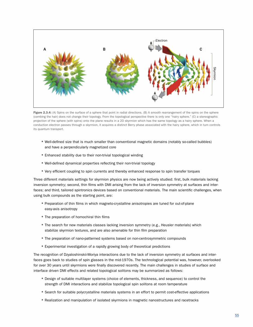
55
• Well-defined size that is much smaller than conventional magnetic domains (notably so-called bubbles) and have a perpendicularly magnetized core
• Enhanced stability due to their non-trivial topological winding
• Well-defined dynamical properties reflecting their non-trivial topology
• Very efficient coupling to spin currents and thereby enhanced response to spin transfer torques
Three different materials settings for skyrmion physics are now being actively studied: first, bulk materials lacking inversion symmetry; second, thin films with DMI arising from the lack of inversion symmetry at surfaces and inter-faces; and third, tailored spintronics devices based on conventional materials. The main scientific challenges, when using bulk compounds as the starting point, are:
• Preparation of thin films in which magneto-crystalline anisotropies are tuned for out-of-plane easy-axis anisotropy
• The preparation of homochiral thin films
• The search for new materials classes lacking inversion symmetry (e.g., Heusler materials) which stabilize skyrmion textures, and are also amenable for thin film preparation
• The preparation of nano-patterned systems based on non-centrosymmetric compounds
• Experimental investigation of a rapidly growing body of theoretical predictions
The recognition of Dzyaloshinskii-Moriya interactions due to the lack of inversion symmetry at surfaces and inter-faces goes back to studies of spin glasses in the mid-1970s. The technological potential was, however, overlooked for over 30 years until skyrmions were finally discovered recently. The main challenges in studies of surface and interface driven DMI effects and related topological solitons may be summarized as follows:
• Design of suitable multilayer systems (choice of elements, thickness, and sequence) to control the strength of DMI interactions and stabilize topological spin solitons at room temperature
• Search for suitable polycrystalline materials systems in an effort to permit cost-effective applications
• Realization and manipulation of isolated skyrmions in magnetic nanostructures and racetracks
Figure 2.3.4: (A) Spins on the surface of a sphere that point in radial directions. (B) A smooth rearrangement of the spins on the sphere (combing the hair) does not change their topology. From the topological perspective there is only one “hairy sphere.” (C) a stereographic projection of the sphere (with spins) onto the plane results in a 2D skyrmion which has the same topology as a hairy sphere. When a conduction electron passes through a skyrmion, it acquires a distinct Berry phase associated with the hairy sphere, which in turn controls its quantum transport.
A B C
ElectronS
kyrmion

56
Last but not least, significant progress has been made in recent years regarding the role of DMI in spintronics con-cepts based on conventional materials. These promise major technological advances when combined with skyrmi-ons and related topologically non-trivial spin textures. Major opportunities arising from these activities and results in the context of skyrmions and topologically non-trivial spin textures are:
• Development of structures and methods to reduce the stray field arising from artificial domain wallsand synthetic skyrmions
• Tailored design of interfacial Dzyaloshinskii-Moriya interactions to stabilize skyrmion textures at roomtemperature for future nanofabricated prototypical spintronic building blocks based on the extensiveexperience of the thin film community in designing artificial superlattice structures
In view of the specific properties of skyrmions, in particular their topological stability and coupling to transport, they promise major advances including the following:
• Increased density for magnetically encoded information
• Greater efficiency of spin transfer torque based devices such as racetrack memories
• Simplification of nano-oscillators
• Realization of dissipationless high-frequency electronics
Skyrmions may also provide a starting point for neuromorphic data processing based on reconfigurable multi-dimen-sional spin arrays and novel multi-functionalities.
Valleytronics: Quasiparticles in semiconductors can be labeled not only by band and spin but also by valley. In the case of single-layer transition metal dichalcogenides, strong spin-orbit coupling makes the valley degree of freedom particularly accessible, suggesting that it could be the basis of a new technology referred to in recent publications as “valleytronics” [189-193]. Operation of useful valleytronic devices requires either optical or electrical control of the valley degree of freedom, which is difficult to achieve in an inversion-symmetric system. Recently, monolayer molybdenum disulfide (MoS2) has been identified as a candidate material where these difficulties can be partly over-come by utilizing the material’s lack of inversion symmetry.
MoS2 is a 2D direct band gap semiconductor with a staggered honeycomb lattice structure. Due to the broken inver-sion symmetry of the monolayer, electrons in the two valleys live in an effective magnetic field, described by a Berry curvature, that is equal but opposite in sign in the two valleys. The Berry curvature gives rise to an anomalous veloc-ity of the electrons, which when biased experience opposite Lorentz forces due to the effective field and therefore move in opposite directions under the action of an electric field.
Figure 2.3.5: (A) Valley-dependent optical selection rules in monolayer MoS2 indicating the opposite clockwise and counterclockwise hopping motions of electrons in two different valleys due to opposite Berry curvatures and therefore opposite effective magnetic fields. (B) Schematic of anomalous Hall effect induced by circularly polarized light and net valley polarization. An image of the Hall bar device displays the transport measurement configuration.
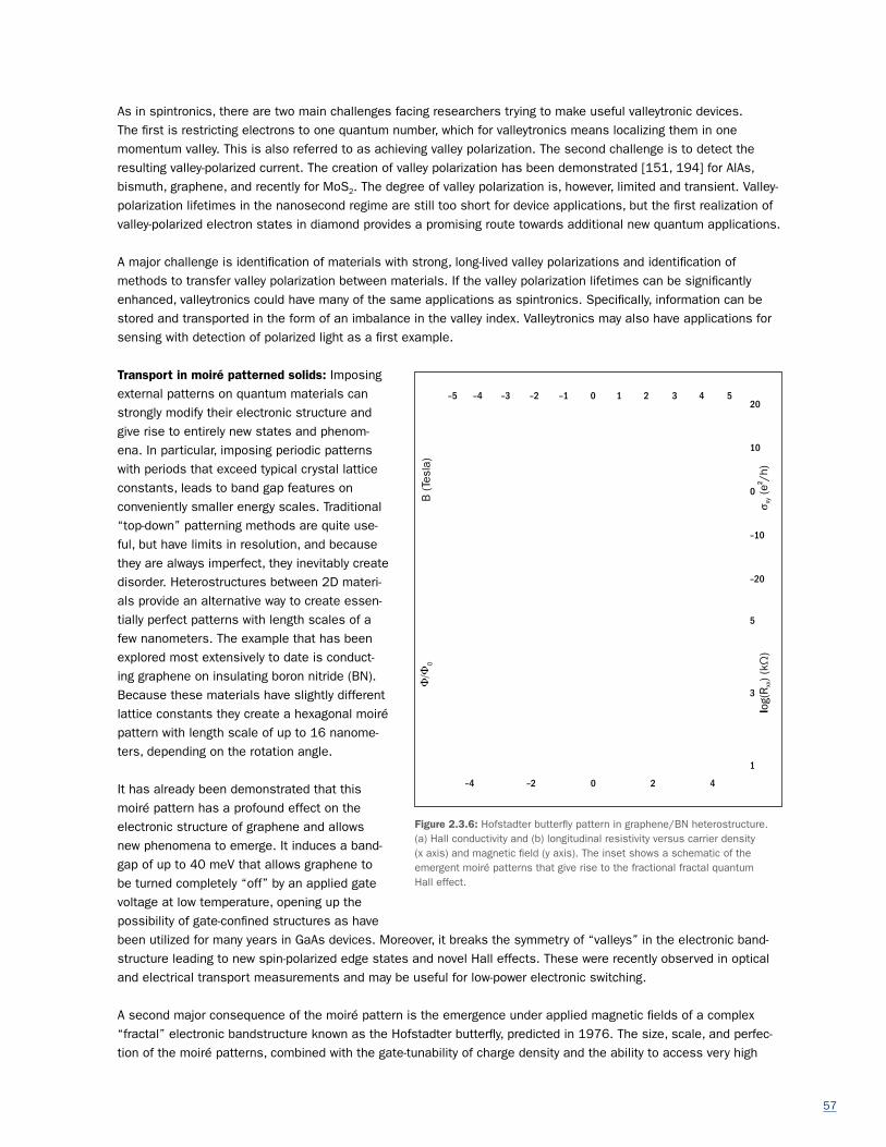
57
As in spintronics, there are two main challenges facing researchers trying to make useful valleytronic devices. The first is restricting electrons to one quantum number, which for valleytronics means localizing them in one momentum valley. This is also referred to as achieving valley polarization. The second challenge is to detect the resulting valley-polarized current. The creation of valley polarization has been demonstrated [151, 194] for AlAs, bismuth, graphene, and recently for MoS2. The degree of valley polarization is, however, limited and transient. Valley-polarization lifetimes in the nanosecond regime are still too short for device applications, but the first realization of valley-polarized electron states in diamond provides a promising route towards additional new quantum applications.
A major challenge is identification of materials with strong, long-lived valley polarizations and identification of methods to transfer valley polarization between materials. If the valley polarization lifetimes can be significantly enhanced, valleytronics could have many of the same applications as spintronics. Specifically, information can be stored and transported in the form of an imbalance in the valley index. Valleytronics may also have applications for sensing with detection of polarized light as a first example.
Transport in moiré patterned solids: Imposing external patterns on quantum materials can strongly modify their electronic structure and give rise to entirely new states and phenom-ena. In particular, imposing periodic patterns with periods that exceed typical crystal lattice constants, leads to band gap features on conveniently smaller energy scales. Traditional “top-down” patterning methods are quite use-ful, but have limits in resolution, and because they are always imperfect, they inevitably create disorder. Heterostructures between 2D materi-als provide an alternative way to create essen-tially perfect patterns with length scales of a few nanometers. The example that has been explored most extensively to date is conduct-ing graphene on insulating boron nitride (BN). Because these materials have slightly different lattice constants they create a hexagonal moiré pattern with length scale of up to 16 nanome-ters, depending on the rotation angle.
It has already been demonstrated that this moiré pattern has a profound effect on the electronic structure of graphene and allows new phenomena to emerge. It induces a band-gap of up to 40 meV that allows graphene to be turned completely “off” by an applied gate voltage at low temperature, opening up the possibility of gate-confined structures as have been utilized for many years in GaAs devices. Moreover, it breaks the symmetry of “valleys” in the electronic band-structure leading to new spin-polarized edge states and novel Hall effects. These were recently observed in optical and electrical transport measurements and may be useful for low-power electronic switching.
A second major consequence of the moiré pattern is the emergence under applied magnetic fields of a complex “fractal” electronic bandstructure known as the Hofstadter butterfly, predicted in 1976. The size, scale, and perfec-tion of the moiré patterns, combined with the gate-tunability of charge density and the ability to access very high
Figure 2.3.6: Hofstadter butterfly pattern in graphene/BN heterostructure. (a) Hall conductivity and (b) longitudinal resistivity versus carrier density (x axis) and magnetic field (y axis). The inset shows a schematic of the emergent moiré patterns that give rise to the fractional fractal quantum Hall effect.
1.0
0.8
0.6
0.4
0.2
0
40
30
20
10
0
n/n0
Vg (Volts)
Φ/Φ
0
log(
Rxx) (k
Ω)
20
10
0
–10
–20
5
3
1
–5 –4 –3 –2 –1 0 1 2 3 4 5
–4 –2 0 2 4
σ xy (
e2 /h)
B (Te
sla)

58
magnetic fields, has enabled the first detailed observation and study of the Hofstadter butterfly. Moreover, in the cleanest samples, new states emerge that have not yet been explained theoretically.
A major challenge is to discover new materials combinations in addition to graphene on graphene and graphene on hexagonal boron nitride, which yield high-quality moiré patterns. For technological applications, by providing a new class of semiconductors with new types of strongly carrier-dependent electronic properties, there is an opportunity to create new types of field-effect devices with applications in low-power electronic devices.
Thrust 3c: Dynamically Visualize and Manipulate Quantum Materials
While the discovery of quantum mechanics is over a century old, it is only now that we are synthesizing and explor-ing materials where the quantum behavior leads to collective phenomena that defy a classical explanation. The degree to which quantum mechanics plays a role in determining these bizarre properties can be quantified by the amount of coherence and entanglement that is present. Since many quantum processes are coherent only over short time scales (femtoseconds or less) and length scales (nanometers or less), it is a challenge to visualize and manipulate this quantum behavior. A path forward is enabled by ultra-fast pump/probe experiments applied to systems where quantum effects predominate, even at room temperature. This thrust is focused on developing this line of scientific inquiry from its current infancy to a broad-based research field where quantum diagnostics and the ability to control quantum effects in materials becomes commonplace. We anticipate that a wealth of novel devices and applications will emerge to exploit these remarkable behaviors.
One focus of this thrust is systems that are driven by an external field (called a pump) for the purpose of precisely controlling the underlying physical phenomena. With the advent of ultra-short light pulses with widely tunable wavelengths, a broad range of different experimental pumps and experimental probes can be applied to quantum materials. By controlling the delay time between the application of the pump and the application of the probe, one can directly measure the time-dependence of the response of quantum materials to the driving fields, and one can even control what the response will be by driving the system into a new state of matter. Unlike more conventional methods for tuning collective quantum behavior in quantum materials (including chemical doping, pressure, and tem-perature), light interacts with matter in many distinct ways: directly exciting electrons; coherently exciting phonons, spin waves, or plasmons; and by modifying the energy landscape over which electrons propagate. Combining these offers versatile control over electronic, magnetic, and photonic phenomena in quantum materials.
Scientific Objective: The overarching goal of this thrust is to provide a means to examine, understand, and control quantum materials by harnessing their coherence and entanglement. There is no single experimental or theoretical method that will achieve this goal, so we describe a range of different foci that serve as the scientific goals for this work.
In pump/probe experiments, a strong pump pulse excites a quantum material in a specific fashion and then, after some time delay, a probe pulse interrogates the transient state of the system. Since the pump pulse often involves extreme field strengths compressed into ultra-short light pulses, it is possible to drive the quantum material far from equilibrium. Indeed, it is precisely this driving, that takes us beyond the linear-response regime and allows pump/probe experiments to enter new realms of physical behavior. For example, the pump can modify the energy landscape to the extent that the system is transformed into a new metastable hidden phase, which is not part of the equilibrium phase diagram, or the field can dress the electronic bandstructure so that it creates new states of matter, such as topological Floquet states (see the sidebar “Transient Floquet-Bloch States”). In other cases, the pump can be tuned in resonance with a particular low-energy excitation to drive the system far from equilibrium. A remarkable example of the latter behavior is offered by recent observations of enhanced superconducting correla-tions by resonant excitation of a coherent phonon [197, 198].
Coupling the pump and probe pulses with plasmonic structures provides a novel means to enhance the electric fields and to restrict the spatial extent of the pump or probe (see the sidebar “Plasmonics and Near-field Optics for Exploring and Exploiting Nanoscale Non-equilibrium Phenomena in Quantum Materials”). For example, magnetic bits in nanostructures can be individually switched from one state to another with all optical driving fields, and plasmonic

59
excitations can be imaged on the nanoscale. As these techniques mature, they can be employed to image dynamical quantum-mechanical effects over a range of length scales, which could elucidate the critical dynamics of quantum phase transitions in materials like high-temperature superconductors.
Defect centers in semiconductors and insulators provide another avenue for controlling and tuning quantum effects in materials. The relatively isolated defects possess spin degrees of freedom that can be entangled with their neigh-bors (even at room temperature) and can be stored for long periods of time within nuclear spin degrees of freedom. By manipulating the properties of entanglement and coherence with different forms of driving fields, one can develop protocols that control these quantum degrees of freedom to the extent that they could be employed as computa-tional devices within the quantum computing paradigm. Quantum degrees of freedom also could be employed as sensitive detectors of different physical phenomena. For example, the general area of understanding spin dynamics and how the quantum-mechanical exchange interaction changes as a function of time and external environments is a critical area of science that underlies many different future technologies.
Finally, a robust development of theory is required to help to process, understand, and exploit these new phenom-ena. In recent years there have been significant advances in computational methods to treat the quantum many-body problem beyond equilibrium, and now these theories can be applied to experimental challenges within this thrust. However, additional theoretical advances are needed to address time scales long enough to simulate the different relaxation mechanisms of transiently excited quantum materials.
Quantum materials can be profoundly manipulated with strong transient electric fields. Exploring field effects on ultra-short time scales can provide unique information about electron-electron and electron-phonon interactions. These interactions can scatter electrons and allow them to equilibrate and thermalize over time after the pump is turned off. These processes are poorly understood but important for many applications of quantum materials.
Finally, the complex interplay of critical fluctuations and disorder gives rise to puzzling properties and ambiguities in interpretation that have slowed progress. Local transport and optical probes that resolve transient order can provide critical information on the appropriate length and time scales. Many new phenomena can be imaged, including pho-ton dressed electronic states, hidden phases, and nonequilibrium relaxation pathways.
Drive ultra-fast switching and phase transitions: Pump-probe experiments with time resolution on the order of femtoseconds or less can monitor the evolution of ordered phases in the presence of large driving fields. This includes visualizing electronic, magnetic, and structural properties of quantum materials and the associated ultra-fast dynamics. By coherently exciting particular collective modes (phonons, magnons, etc.), these experiments can elucidate the interplay between the time domain and real space and the coherent oscillations of order parameters as they relax back to equilibrium (see Sidebar “Photon-Electron Hybrid States” ). Coherent excitation is also suit-able to investigate the roles topology plays in the physics of quantum materials. Finally, coherent excitation offers experimental access to novel phenomena, such as light-induced phase transitions, which examine the details of how transient (or metastable) magnetism, superconductivity, charge-ordered states, and exciton and polariton conden-sates evolve during a phase transition. One key to success is to image dynamics on the appropriate length and time scales where the changes in the properties of the systems are the greatest.
Exploit strong-field dressing of electronic states: As strong electric fields drive electrons in quantum materials, they also modify the electronic band structure. A new state of matter that can be created is the Floquet-Bloch state, which is periodic in time (the simplest example being the Wannier-Stark ladder), and hence can be determined by a Bloch-like theorem for the energy spectra, but in the time domain. By choosing appropriate polarizations of light, the topological properties of these Floquet-Bloch states can also be manipulated and controlled.
Stimulating electrons with large electric fields can drive a system into transient or metastable hidden phases that are not part of any equilibrium phase diagram. These hidden phases have different, perhaps tunable, properties, which can be explored for applications. In addition, one might be able to reversibly switch between known and hidden phases on ultra-fast time-scales, which can have many different applications for ultra-fast electronics.

60
The “devil is in the details” for these systems. Can we predict the properties of hidden phases and how can a specific hidden phase be accessed and stabilized? Can we develop techniques to measure the entangled order parameters and unravel the pathways between different phases? Can we tailor the properties of quantum materials to develop specific hidden phases with desired properties?
Manipulate entanglement in quantum materials: While atomic-scale defects are often viewed as liabilities within conventional systems, they offer a powerful platform to create and control coherence and new families of quantum materials. Using ion implantation or electron beam patterning, arrays of defects may be created within or at the surface of semiconductors that give rise to individual or interacting single electronic spin states. Advanced den-sity functional methods have been remarkably successful in predicting broad classes of materials that exhibit this behavior, including diamond, silicon carbide, zinc oxide, and a growing list of other systems. Using a combination of microwave and optical spectroscopy, these quantum states may be initialized, manipulated with optical, magnetic, or electrical fields, and read-out with high fidelity from ambient to cryogenic temperatures. In addition to quantum con-trol of electron spins, precise manipulation of the hyperfine interaction has led to control of single nuclear spins with substantially longer coherence times and the creation of “engineered” quantum entanglement in solids. Recently, manipulation of these interactions has enabled the demonstration of optically connected long distance entangle-ment and pathways for teleportation [199].
The ability to create and manipulate entanglement in quantum materials offers extraordinary opportunities to explore fundamental questions in condensed matter and quantum physics (see the sidebar “Creating and Controlling Quantum Materials with Defect Spins in Semiconductors”). Materials that host entanglement include homogeneous semiconductors as well as heterostructures to investigate the transport of coherent states within and across interfaces. The precise control and measurement of quantum states provide a means to explore routes of decoherence in solids, and theoretical protocols that may be implemented to maintain coherence (such as dynam-ical decoupling). The ability to create individual pairs and ensembles of fully entangled states may also be used as a resource for processing and communicating quantum information, and it may be used as a means to develop new entanglement-based sensing instrumentation with the potential to break the classical shot noise limit and operate at limits of quantum uncertainty.
Create the experimental tools for the next generation of pump/probe experiments: Non-equilibrium pump-probe studies of quantum materials will require new sources of intense pulsed electric fields that span energies ranging from THz frequencies to x-rays but also have femtosecond or shorter temporal extent. These sources need to be combined with stable spectroscopic measurement tools to allow for different forms of electronic, magnetic, and structural characterizations of quantum materials. One new development involves employing advanced plasmonics to control and manipulate electromagnetic radiation at the nanoscale for enhanced pump/probe experiments and for imaging applications. Development among many different platforms ranging from table-top resources to accelera-tor-based facilities will be required.
A key challenge will be the visualization of different quantum phenomena on the ultra-fast time scale. Here new tech-niques like ultra-fast coherent diffraction imaging in 3D, transient diffraction gratings, and plasmonic controls will be required to develop novel imaging resources that will functionally image the quantum behavior as it is happening. Advanced imaging of surfaces, bulk, buried interfaces, and functioning systems will also be crucial to piece together the different aspects of these complex materials.
In a different regime, neutron scattering offers the possibility of detailed bulk characterization of relaxing quantum materials beyond the micro-second time scale. Ongoing advances in steady state and pulsed source instrumenta-tion make this an attractive area that seems ripe for development.
Provide theoretical understanding and predictive capability for enhancing coherence and entanglement in quan-tum materials: While recent years have seen much success in numerical simulation and theoretical development of the many-body problem in equilibrium, there is a dearth of robust methods to describe quantum materials beyond equilibrium. Concerted efforts are required to develop theoretical methods in this regime. While computers have
61
become powerful enough to simulate the nonequilibrium many-body problem, many equilibrium methods fail, so we need to focus on the development of new algorithms and new techniques that can address quantum materials out of equilibrium. The resulting theory and computation will be applied to the different experimental phenomena discussed above.
One of the critical issues within the theory is the development of techniques that can simulate both the transient behavior and the return towards a steady state (or equilibrium). Long-time relaxation effects, and the precise meth-ods needed to transfer (or enhance) coherence and entanglement also need to be determined and developed.
Summary: Quantum matter driven far from equilibrium is one of the most interesting and most poorly understood states of matter. We hope by being able to fully understand this behavior, we will be able to also control electron dynamics, which enables sophisticated tunable devices that operate on ultra-fast time scales. This research can lead to the discoveries of new states of matter; can create enhanced coherence over wider length and time scales; and can pave the way to engineering novel quantum phenomena. Visualizing quantum effects in real and momentum space will enable broad understanding of the underlying physics by
• Accessing states that are inaccessible in thermal equilibrium
• Determining novel ways of inducing phase transitions
• Providing new insights into coherent light-matter interactions
• Driving the development of revolutionary scanning, imaging, and spectroscopic methods
• Creating new theoretical and computational methods to describe and predict properties of quantum materials far from equilibrium
• Tailoring novel quantum materials that support hidden phases
This work can have a long-term positive impact on energy technologies. Since many electronic devices employ the nonlinear response characteristics of the materials from which they are made, understanding and manipulating these properties is key to achieving the novel devices and applications of the future. In particular, this work impacts technologies that involve the following: ultra-fast and energy-efficient switching for information processing and ener-gy-efficient computation; ultra-high density magnetic storage; manipulating coherence and entanglement for novel quantum-based technologies; and pushing quantum materials far from equilibrium to enter new regimes, where even more complex phenomena can be employed in devices.

62
PHOTON-ELECTRON HYBRID STATES
Modern technology relies on devices that are built from materials with distinct properties. Depending on the application, we use conductors, insulators, and transparent or opaque materials to get a particular job done. Traditionally, when building a new device, we are limited to using existing materials with their intrinsic properties.
Coherent coupling of light with materials can fundamentally change this paradigm. The idea is to use light to modify the properties of an existing material and engineer a novel state with desired properties. In conventional materials, the charac-ter of the electronic states, i.e., how the energy of electrons changes with respect to their momentum and whether there are empty states immediately accessible above the filled states, determines the properties of the material, like its response to being heated, or whether it is opaque and shiny or transparent. To change these properties, one usually needs to change the chemical composition of the material, which is impractical and cannot be done in real time.
It has recently been shown that the interaction of photons with electrons can create new photon-electron hybrid states in solids [200, 201]. This figure shows a measurement of the energy-momentum relationship of electrons as a function of time during excitation by a femtosecond laser pulse. At the peak of the laser pulse, new hybrid photon-electron states are formed as replicas of the original states. That these new hybrid states behave in exactly the same way as the conventional electronic states opens up an exciting path to temporarily alter the properties of a quantum material by changing the light it interacts with rather than the material itself.
Photon-electron hybrid states offer exciting possibilities for new technologies. For example, conventional materials just dis-play their equilibrium phases, which are found at the minimum of their energy landscape. Frequently, there are other phases that exist in the phase diagram that are not stable, so they are never observed in nature. With the coherent coupling of light with materials, it may be possible to access unstable phases yielding many different quantum phases for a given mate-rial. By tuning the properties of the incident light (such as its intensity, color,or polarization), one can change the resultant material properties, i.e., from metallic to insulating. Light excitation can quickly be switched on-or-off and can be spatially patterned, opening up multiple new ways of designing and creating new devices.

63
PLASMONICS FOR EXPLORING AND EXPLOITING NANOSCALE NON-EQUILIBRIUM PHENOMENA IN QUANTUM MATERIALS
Plasmons are collective oscillations of electrons across the surface of a conductor that can interact with photons. The field of plasmonics harnesses this coupling of electrons and photons to break the “diffraction limit” and see objects smaller than the wavelengths of visible light. The stunning success of plasmonics for manipulating light at the nanoscale has been empow-ered by imaginative engineering designs and state of the art nano-fabrication. By taking advantage of plasmonics principles, major advances in quantum materials can be achieved. A recent example is displayed in Panels A–C. A plasmonic antenna lithographically defined on the surface of a magnetic material, terbium iron cobalt (TbFeCo), serves to amplify the light-mat-ter interaction [202]. The use of ultra-short optical laser pulses as illustrated in the figure opens up novel ways to coherently control the spin motion on the length and time scales of the exchange interaction [203] as revealed by novel x-ray holography techniques [204]. This line of research opens a new chapter in the studies of magnetism, which until recently focused on examining systems close to their thermodynamic equilibrium. Plasmonics could make future data storage devices signifi-cantly faster while dramatically decreasing the energy required for data storage and processing.
The fundamental optical and electronic properties of elemental metals, the prevailing plasmonic media, are difficult to alter using external stimuli, a limitation particularly restrictive in applications requiring modification of the plasmonic response at sub-picosecond time scales. This handicap has prompted the search for alternative plasmonic media [205–207] with graphene (a single atomically thin sheet of carbon) emerging as one of the most capable candidates [208]. Recent innovations in instru-mentation for pump-probe spectroscopy and imaging at the nanoscale [209–211] have allowed the investigation of non-equilib-rium plasmons in graphene (Panels D, E). Plasmons were activated with femtosecond optical pulses in a specimen of graphene that otherwise lacked an infrared plasmonic response at equilibrium. The results revealed novel aspects of carrier relaxation in graphene-based heterostructures in the regime where non-equilibrium electronic temperature is approaching several thousand Kelvin [212]. The analysis of plasmonic images allows one to explore new phenomena in the medium that support plasmons, but has so far been underutilized in the field of quantum materials.
A B C
Inital Single shot
M-
M+
Next single shot
D E
pump
1000
950
900
850
0 200 400nm
Freq
uenc
y (c
m1
) Max
Min
S(ω
,x)
Panels A–C: Antenna-mediated ultra-fast magnetic switching is reproducible and reversible. (A) Initial magnetic contrast around an antenna after magnetic sat-uration in a field of 1.6 T. (B) Magnetic contrast after first femtosecond laser pulse of 3.7 mJ/cm2. A small domain with a FWHM of 53 nm is switched. (C) The magnetic domain is switched back in the original direction by the next laser pulse. Panels D–E: Pump-probe nano-im-aging of nonequilibrium plasmons in graphene. (D) The pump-probe nano-in-frared setup is a hybrid of ultra-fast lasers and an atomic force microscope. (E) Pump-probe images of the near fieldscattering amplitude data revealing theenergy- momentum relation of photo-in-duced plasmons at zero time delay. Theblack dashed lines mark the peaks ofthose traces.
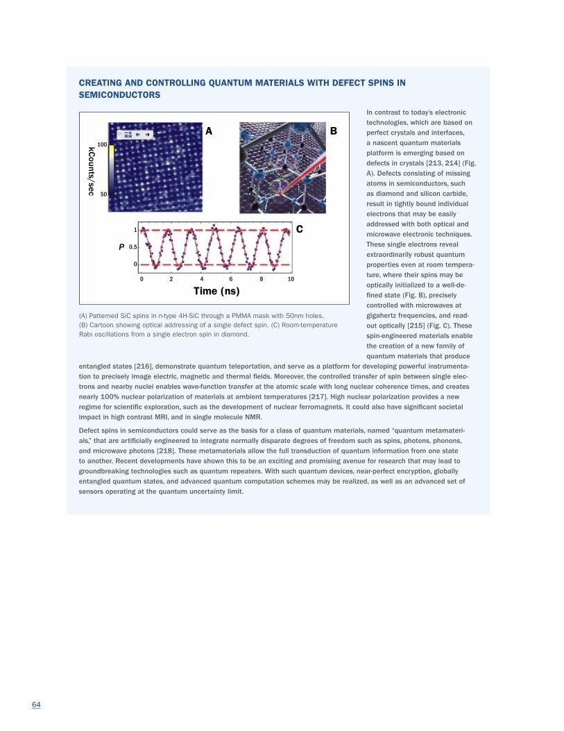
64
CREATING AND CONTROLLING QUANTUM MATERIALS WITH DEFECT SPINS IN SEMICONDUCTORS
In contrast to today’s electronic technologies, which are based on perfect crystals and interfaces, a nascent quantum materials platform is emerging based on defects in crystals [213, 214] (Fig. A). Defects consisting of missing atoms in semiconductors, such as diamond and silicon carbide, result in tightly bound individual electrons that may be easily addressed with both optical and microwave electronic techniques. These single electrons revealextraordinarily robust quantum properties even at room tempera-ture, where their spins may be optically initialized to a well-de-fined state (Fig. B), precisely controlled with microwaves at gigahertz frequencies, and read-out optically [215] (Fig. C). These spin-engineered materials enable the creation of a new family of quantum materials that produce
entangled states [216], demonstrate quantum teleportation, and serve as a platform for developing powerful instrumenta-tion to precisely image electric, magnetic and thermal fields. Moreover, the controlled transfer of spin between single elec-trons and nearby nuclei enables wave-function transfer at the atomic scale with long nuclear coherence times, and creates nearly 100% nuclear polarization of materials at ambient temperatures [217]. High nuclear polarization provides a new regime for scientific exploration, such as the development of nuclear ferromagnets. It could also have significant societal impact in high contrast MRI, and in single molecule NMR.
Defect spins in semiconductors could serve as the basis for a class of quantum materials, named “quantum metamateri-als,” that are artificially engineered to integrate normally disparate degrees of freedom such as spins, photons, phonons, and microwave photons [218]. These metamaterials allow the full transduction of quantum information from one state to another. Recent developments have shown this to be an exciting and promising avenue for research that may lead to groundbreaking technologies such as quantum repeaters. With such quantum devices, near-perfect encryption, globally entangled quantum states, and advanced quantum computation schemes may be realized, as well as an advanced set of sensors operating at the quantum uncertainty limit.
(A) Patterned SiC spins in n-type 4H-SiC through a PMMA mask with 50nm holes. (B) Cartoon showing optical addressing of a single defect spin. (C) Room-temperature Rabi oscillations from a single electron spin in diamond.
A B
C
Time (ns)0 2 4 6 8 10
1
0.5
0
100
50
kCounts/sec
P

65
2.4 PRD 4 — DESIGN REVOLUTIONARY TOOLS TO ACCEL-ERATE DISCOVERY AND TECHNOLOGICAL DEPLOYMENT OF QUANTUM MATERIALS
The remarkable properties of quantum materials that are generating such keen scientific interest — including the
ability to alter their electronic, structural, or magnetic state through external stimuli, or transport spin and charge
with extreme efficiency — also pose immense challenges to the experimental and theoretical work that is required
to understand and exploit them. PRD 4 calls for development of the necessary tools to address these challenges,
affecting the synthesis, characterization, and theoretical treatment of quantum materials. Key challenges include
establishing appropriate methods to grow and manipulate complex and nano-structured quantum materials with
desired purity and control of dopants and defects from a single atomic layer on up to bulk crystals, including
where appropriate in situ characterization and feedback, and the discovery of materials with improved properties
based on these new techniques. Other challenges entail characterizing quantum materials and learning how to
manipulate their properties on all length and time scales relevant to function. This includes developing appropri-
ate tools to reveal the often subtle forms of emergent and topological order that such materials can harbor, and
predicting the fundamental properties of quantum materials, such as their tendencies to emergent order, and
their behavior far from equilibrium and in the presence of disorder. Progress in these areas will enable the science
visions expressed in the other PRDs, and will also have a broad impact across wide ranges of materials, nano,
and energy sciences, where traditional tools lack the resolution, speed, and precision required to keep pace with
current demand.
2.4.1 Introduction
The discovery, growth, and characterization of quantum materials is limited by the physical tools available. Many of the tools currently used are highly sophisticated, but there remains room for significant enhancements that would directly increase the rate at which promising new materials are identified, prepared in appropriate form, characterized, and, where relevant, utilized for applications. This PRD focuses on the most pressing needs, affecting synthesis, characterization, and theory.
In terms of synthesis, the development of new tools and techniques serves to broaden the palette of possible materials. Recent examples (discussed in greater depth in Section 3.6.1 of this report) include the development of new furnace technologies that enable crystal growth in extreme physical regimes, new deposition tools for detailed in situ characterization, and new methods to pattern and process materials that enable entirely new classes of measurements and applications. There remains, however, ample opportunity for further improvements in all of these areas, which, combined with an emphasis on exploratory synthesis, will lead to an increased rate of discovery of promising materials.
In terms of characterization, there are many rich opportunities for new tools to make, probe, and design specific functions. For example, a decade ago many measurements of the properties of quantum materials (e.g. electronic,
66
magnetic, and transport properties) used very specialized experimental setups that were developed and used by dedicated experts and measured only a single property of the material in isolation. Neutron and synchrotron x-ray scattering experiments could be conducted only with the help of experts, and their slow speed combined with limited access to advanced facilities meant that comparing different samples or attempting iterative design was a painstak-ing process. More recently, a wide range of advanced tools have provided unprecedented insights into the function of complex materials, drawing on multiple imaging and spectroscopic tools that were previously unimaginable. Further advances can be envisioned that would dramatically affect the rate at which materials are evaluated and improved for specific functions and applications. There is a need to develop completely new forms of measurements and analysis to access the distinguishing characteristics of quantum materials such as entanglement and topology and collective time dependent properties of quantum materials driven beyond equilibrium. To access a broader space of quantum matter and achieve a deeper understanding of complex behaviors of quantum materials, there is a need for sophisticated characterization of quantum materials under extreme thermodynamic conditions and in hidden phases beyond thermal equilibrium.
A specific example of how new tools can accelerate the deployment of quantum materials is provided by recent work to develop FePt thin films and nanoparticles for next-generation magnetic recording media. Due to strong couplings among the spin, charge, and lattice degrees of freedom, this material exhibits extremely large magnetocrystalline anisotropy and is thus a candidate for achieving ~4 Tb/in2 recording. However, these materials are chemically disordered, which makes them challenging to grow, probe, and model. A fundamental understanding of 3D crystal defects, local chemical ordering, and the dynamic magnetic properties of FePt films and nanoparticles, from atomic to mesoscale, is still lacking. Thus, to improve material design, growth, and deployment, new tools for imaging thin films and nanoparticles on all relevant length and time scales are needed. As discussed in the following sections, these new tools include advanced atomic resolution electron tomography to precisely determine the 3D positions of individual atoms, as well as point defects. The microscopic origin of the large magnetic anisotropy lies in the local structure around magnetic ions; this can be probed by a combination of dynamic x-ray coherent lensless micro-scopes using both large-scale facilities and tabletop x-ray sources. Nano-optical probes can also be used to charac-terize nanoscale heterogeneities. Multi-dimensional and multi-length scale probes, when combined with advanced theory, could profoundly expand our understanding of how grain boundaries, domains, point defects, and chemical ordering affect local charge and orbital ordering (magnetic) and transport properties, i.e., how a heterogeneous material functions.
Crystalline quantum materials also present profound experimental challenges. While insulating materials with long-range magnetic order have magnon quasi-particles that can be probed in great detail through inelastic neutron scattering, quantum spin liquids are characterized by the entanglement of the ground state and by topological qua-si-particles that mainly produce broad scattering continua [11, 221]. Progress towards understanding such materi-als and making contact with the corresponding theoretical work will require the use of complementary experimental techniques and new methods to conduct and analyze inelastic neutron and x-ray scattering experiments.
Closely coupled to the needs described above is a similar need for improved theoretical and computational tools. While theory is already central in the interpretation of experiments, the challenge lies in describing the physical properties of materials where strong electron-electron interactions lead to a failure of mean field approaches that treat each electron as moving in a self-consistent averaged environment resulting from all other electrons. Analytical and computational methods that go beyond this mean field approximation and treat the full many-electron problem have seen significant progress in the past decade and could have greatly increased applicability in the near term. Because these powerful methods are computationally expensive, it is also important to develop approaches that combine them with standard, less expensive methods, such as density functional theory, that are sufficient for most of the electrons. While traditional theory may focus on bulk properties near thermal equilibrium, a more informative encounter between theory and experiment is possible when the theoretical work proceeds to predict complex prop-erties such as two-point correlation functions for comparison to scattering and spectral functions for comparison to ARPES. Likewise a new class of experiments now probes far-from-equilibrium dynamics of electrons in quantum materials. Improved far-from-equilibrium theories would help extract the maximum amount of scientific understand-ing from such cutting-edge experiments.
67
2.4.2 Scientific Challenges
The attractiveness of quantum materials — with their unusually rich phase diagrams that support useful crystallo-graphic, electronic, magnetic, and superconducting phases — is at the same time the origin of the immense challenge to understand and exploit them. As a result, many quantum materials, whether recently discovered or under scrutiny for decades, still defy comprehensive understanding and hence cannot be fully exploited for technology. Over the past decade, growth techniques, instrumentation, and theory relevant to quantum materials have all advanced significantly (see section 3.6). However, despite these advances, there are still fundamental challenges associated with the syn-thesis and patterning of existing quantum materials, and significant opportunities exist to design and discover new materials systems. No experimental method can simultaneously capture all relevant properties of a quantum material — rather each spectroscopy or imaging technique offers a window into a certain part of the electronic or structural character of the material. Because the unique properties of quantum materials rely on strong couplings, cooperativity, entanglement, and competition on atomic length scales or across nano-interfaces, and dynamics spanning from a few femtoseconds to seconds and even longer time scales, no current theory can accurately model all relevant aspects of a quantum material. Addressing these limitations represents grand challenge science that will accelerate progress in all areas of science covered by this report.
Materials synthesis is crucial for all experimental studies of quantum materials, motivating intense research on the optimal methods to grow/deposit/prepare materials of current interest. Furthermore, the discovery of new quantum materials, or methods to artificially structure them, has been the main continuous source of unexpected discoveries that define the next frontiers of the field. A wide range of new and established synthesis techniques are now employed to create and tune quantum materials in a variety of physical forms, including bulk polycrystalline, single crystal, and amorphous materials, as well as 2D sheets, nanocrystals, thin films, and heterogeneous materials. However, several major scientific challenges must be overcome in order to accelerate the rate at which new materials with desired properties are discovered and synthesized in appropriate form, with appropriate purity, doping, nanostructure, etc. In particular, generalized rules of assembly appropriate for various classes of complex materials must be established, and new/advanced methodologies and tools for synthesis, deposition, and assembly must draw on this understanding, informed, where appropriate, by in situ probes. There is also an ongoing challenge to expand the range of exploratory synthesis by leveraging new and existing synthesis approaches to encompass a wider phase space of materials. Addressing these challenges would advance the field from “materials by design” to “synthesis by design”; the logical extension of the effort embodied by the recent Materials Genome Initiative. (see www.mgi.gov)
Revolutionary advances in capabilities associated with electron, neutron, laser, and x-ray techniques have led to a significant improvement in the understanding of many quantum materials. At the national laboratories, access to high magnetic fields and x-ray and neutron scattering and imaging has expanded. Since 2010, there have also been revolutionary advances in light sources spanning the x-ray to the THz region of the spectrum, with exquisite control over the spectrum, pulse duration, and polarization. To accelerate the development and understanding of quantum materials with specific collective properties, such advanced spectroscopic methods covering time scales from femtoseconds to nanoseconds over a wide range of temperatures and fields will be important along with theoreti-cal methods that link chemistry and structure to the corresponding spectra and desired materials properties. New computational imaging techniques that harness powerful algorithms have pushed electron imaging to atomic reso-lution in 3D, and enabled extreme ultraviolet and x-ray imaging with wavelength-limited spatial resolution for the first time. Advanced spectroscopies can capture all the information about the instantaneous magnetic, electronic, and mechanical properties of a material, which if combined, can lead to dramatic improvements in our ability to manip-ulate quantum materials. While these developments have already greatly accelerated the rate at which the phase space of new quantum materials can be charted, their properties understood, and in some cases deployed in tech-nology, current single-modality tools cannot fully address the challenge of uncovering how the most complex quan-tum materials function. New hybrid imaging and multidimensional spectroscopic techniques would make it possible to probe multiple aspects of quantum matter simultaneously, in effect realizing new quantum microscopes that can coherently manipulate and probe quantum matter, while combining all these techniques with “big data” methods. Development of such tools would accelerate the smart, iterative design of specific functionalities for applications.
68
Finally in theory, grand challenges include correctly accounting for correlations and nanostructure, as well as tackling a problem that is also central to many areas of the physical sciences — how to model a system where the charges, spins, or lattice are not only interacting, but also far-from-equilibrium.
2.4.3 Research Thrusts
This PRD involves three closely linked thrusts that build upon each other: enhanced synthesis (Thrust 4a), new approaches to characterization of quantum phenomena (Thrust 4b), and efficient theoretical methods for static and dynamic states beyond 1-electron paradigms (Thrust 4c).
Thrust 4a: Enhanced Synthesis of Quantum Materials
The objective of this thrust is to obtain new and better quantum materials. The emphasis is therefore on “synthesis science”: new concepts, new methodologies, and new tools applied to the synthesis of quantum materials.
In recent years a major effort has been directed towards the task of predicting a material that exhibits desired properties or functionality. Distinct from this task is the associated scientific challenge of determining appropriate synthesis methods and conditions necessary to realize the predicted materials. This major scientific challenge cross-cuts all of the intellectual questions raised in the other PRDs. Addressing this challenge brings better sam-ples and new materials, both of which are essential to further the major science themes discussed throughout this report. The research directions outlined below are broadly relevant to all materials platforms, from bulk single crystals to thin films to nanocrystals, including thermodynamically stable and metastable phases, crystalline and amorphous phases, and homogeneous and heterogeneous materials, but the required advances in terms of tools, techniques, and understanding necessarily depend upon specifics.
Scientific objective: Materials synthesis plays a central role in the field of quantum materials. The exotic electronic phases discussed throughout this report are not abstract, but exist in real materials (or, in some cases, have every right to exist but are yet to be discovered), and real materials require synthesis. However, there is a fundamental science gap. Specifically, given a prediction for a material, how do you make it? If this question could be universally answered, the field would move from “materials by design” to “synthesis by design”; the logical extension of the approach embodied by the Materials Genome Initiative. In comparison, the field of organic chemistry is very sophisticated: Synthetic methodologies and reaction types exist to make extremely complex molecules that are routinely applied to a wide variety of materials (for example, using the principles of retrosynthetic analysis). A com-parable understanding of inorganic synthesis is lagging, and presents an opportunity and challenge for the field of quantum materials.
This thrust revolves around three inter-related components, which are broadly relevant across all materials platforms:
1. New concepts: establishing generalized rules of assembly for complex materials
2. New methodologies and new tools
3. Expanding the range of exploratory synthesis
There is a natural synergy among these three areas. Progress in the development of new synthetic concepts leads to new methodologies and tools, which in turn expand the range of exploratory synthesis. In the following sections we outline what progress in each of these areas looks like in the context of quantum materials for a variety of materials platforms.
New concepts: establishing generalized rules of assembly for complex materials: The aim of this research direction is to determine, understand, and control reaction/synthesis/ deposition/assembly pathways for metastable, kinetically stabilized, and thermodynamic phases of quantum materials.

69
Approaching the long-term goal of “synthesis by design” requires establishing generalized rules of assembly for complex materials. Such rules are of course different for different materials platforms (bulk, thin film, heterostruc-tures, nanocrystals, etc.), but the basic goal remains the same. These rules provide road maps for synthesis, analo-gous to the role played by equilibrium phase diagrams in the crystal growth of thermodynamically stable compounds, but encompassing now much broader materials regimes such as kinetically stabilized and metastable phases, 2D materials, and thin films. Even the seemingly simple case of thermodynamically stable phases presents major chal-lenges, with large gaps in the current knowledge regarding the nature of structural units present in the melt or in the vapor and the ways in which these units can be controlled to achieve desired materials.
In order to establish such rules for the assembly of complex materials, it is necessary to understand the constituent molecular species, correlations, and dynamics at the growth front as a function of time, motivating in situ charac-terization of liquid and vapor phases. Research in this area will ultimately lead to accelerated exploratory synthesis guided by theoretical input, chemical knowledge, and science/technological drivers. An associated outcome of targeted research in this area will be the generation of databases of reactions and their associated taxonomy.
Bulk synthesis and crystal growth: Classical materials synthesis from melts and fluxes is “blind”: Reactants lead to products and the pathway leading between them is terra incognita; any information about potential intermediates and their histories is lost. This lack of awareness hinders the ability to devise successful synthetic processes for targeted materials. What if we could see all possible phases and associated micro and nanostructures forming in the course of a reaction? If we are to develop a predictive understanding of synthesis to more quickly discover new materials, we will need to know:
• The route: for example, when and how do new phases form during a synthesis protocol and what is
their evolution over time? When do all precursor reagents disappear? When do compounds (reactants,products, and intermediates) appear and then disappear from the reaction medium? Can we designtools and approaches that allow us to observe all crystalline products in a given reaction?
• How does the particular set of starting conditions (reactants, time/temperature profile, and atmo-
sphere) impact the reaction pathway? Can these process constraints be manipulated to improve theproperties and reduce the processing complexity for bulk solids and films prepared? If the desiredcompound happens to be a metastable structure, then a conventional “blind synthesis” will not evenbe able to detect it due to lack of awareness. When does such a compound appear and then disap-pear from the reaction medium?
• Can we classify synthetic reactions in “reaction types” after learning and observing reactivity characteris-
tics and patterns? If possible, such a classification could suggest appropriate methodologies to creatematerials that share a defined structural, compositional, or physical characteristic. Can we use these“reaction types” as a methodological tool to design syntheses pathways for new quantum materials?
If we could answer these questions, we would have a “panoramic” view of reactions and spot all possible phases in a given composition system of interest. The following need to be developed: tools, experiments, and a knowl-edge base designed to unify, for a given reaction, critical calculable and experimentally observable processes and materials occurring during the course of the reaction, and tags with their attributes: stability versus other phases, precursors, kinetic history, etc. This is the gateway to obtaining insights into where new materials may lie and how to synthesize them, and a new way of advancing materials discovery. A closely related challenge would be to make direct connection to “on the fly” computation of diffraction patterns that can guide the processing. A bigger challenge in this area is the “inverse problem” — that is, given some kind of diffraction pattern, and appropriate constraints, what are the kinds of building units that might be in the system? If such things could really be done, one could imagine developing databases of such signatures that could then be interrogated in operando. The under-lying assumption, of course, would be that there are rules for the assembly of such building units (correlations) tied ultimately to the chemistry of the constituent atoms. We know some of these rules today (e.g., building units in phosphate or silicate glasses). The challenge is to expand this understanding to encompass a wider variety of promising materials.

70
Thin film and heterostructures: Thin film growth presents a number of additional degrees of freedom beyond bulk synthesis, providing access both to new materials-control opportunities and associated complexity. Considering first thermodynamic stability, the presence of a substrate can dramatically alter the energetic landscape of the film; well-known examples of such epitaxial stabilization include cubic versus wurtzite GaN or rutile versus anatase TiO2. These effects have largely been used to shift structural phase boundaries known from bulk phase diagrams, such as under hydrostatic or chemical pressure. However, there is significant potential to greatly expand these effects, particularly for ultrathin films. In nanoparticle synthesis, an important finding is that as the particle size is varied, the evolution of the surface/bulk energies can drive structural phase transitions and new atomic arrangements. By analogy, enhancing the role of surface/interface energies in thin films and heterostructures can provide a new synthetic opportunity to create novel crystalline forms of quantum materials. There are large potential synergies to integrate a combined theoretical/experimental efforts to advance this approach.
A second consideration is that thin film growth is by definition a non-equilibrium process. The deviation from equilib-rium can be modest (such as for vapor phase transport [VPT] or MBE) to extreme (such as for highly kinetic regimes of sputtering or pulsed laser deposition [PLD]). These various conditions can create widely different regimes for the stability and density of crystalline defects, both favorable and deleterious. Furthermore, a number of materials are not line compounds, which requires addressing challenges as to whether flux control can be further developed to reduce intrinsically high point defect concentrations. While these kinetic degrees of freedom are known issues, developing a broad perspective spanning various growth techniques can advance the ability to fully utilize the palette of thin film growth techniques to control and tune materials microstructure.
2D materials and nanocrystals: Synthetic routes, kinetics, and reactants during nanocrystal and 2D material synthe-sis based on popular methods such as vapor-liquid-solid growth or chemical vapor deposition largely remain unex-plored, critically limiting the ultimate crystalline quality and size of these nanoscale crystals. For example, despite the remarkable progress in 2D material synthesis which has recently achieved wafer-scale, polycrystalline MoS2 single layers [222, 223], the exact molecular species in the vapor phase given specific precursors and detailed kinetics of nucleation and growth on the substrate as a function of substrate temperature and vapor pressures are essentially unknown. A detailed understanding of the nucleation and growth of 2D materials and nanocrystals on a substrate could lead to large area, single-crystalline 2D layers by controlling nucleation sites, and nanocrystals that are terminated with only the desired crystalline planes. To this end, we will need to know:
• What are molecular species in the vapor phase that lead to 2D materials and nanocrystals?
• How do chemical reactions occur, and do they occur in the vapor phase or during growth?
• How do nucleation and growth depend on growth conditions and substrates, in situ? How do we control
them? Could we exploit reactive force field methods to model nucleation and growth of thin films, thus
providing guidance to crystal growers?
• Once materials are synthesized, how can they be removed from growth substrates without introducing
contamination?
Some of these questions overlap with questions related to bulk synthesis, crystal growth, and thin film deposition. Similar to those cases, in situ and in operando measurement techniques need to be developed, which would allow investigation of kinetically stable as well as transient molecular species during growth.
Recent advances have also shown the promising growth of crystalline 2D materials such as HfSe2 using conven-tional UHV MBE, albeit with sub-micron grain sizes. In this context, we note that the van der Waals bonding of 2D materials relaxes traditional constraints on lattice matching with the substrate, allowing one to explore a wider variety of epilayer-substrate configurations than in conventional epitaxial thin films. Hybrid MBE that combines met-al-organic sources with conventional inorganic solid sources in an UHV environment could provide an alternative and more powerful route toward wafer-scale single crystal growth of such 2D materials by giving access to an expanded parameter space for controlling the kinetics of nucleation and growth. In some cases, in contrast to UHV methods,
71
high-pressure gas phase synthesis methods may be necessary for new 2D materials, such as black phosphorous (phosphorene) thin films [224]. These recent achievements indicate the need for sustained and focused efforts to develop the science of synthesis of 2D materials and nanocrystals.
New methodologies and new tools: The spectrum of accessible quantum materials is limited by the tools available for their synthesis. The development of new/advanced methodologies and tools for synthesis, deposi-tion, and assembly of complex materials, informed where appropriate by in situ probes and connecting to the new concepts discussed above, has the potential to access new physical regimes, and new materials, not previously accessible.
Ways to guide reaction pathways, including accessing kinetically trapped compounds: One challenge in guiding a synthesis to a desired material is the ability to obtain it in the presence of closely lying (in composition, energy, and stability) competing phases. A representative example of an unsolved challenge here is the Bi-O-S superconductor family [225]: There are many different layered structures, but due to equilibrium with gas phases it is not clear how to make them cleanly. We need new approaches to do this. The development of methods that control the kinetic paths of reactions, for example by decreasing the lengths that atoms have to diffuse, is very important. This can be accomplished by using cleverly designed precursors or by learning how to avoid the undesirable phases, but addi-tional innovation is needed.
Synthesis in extreme environments: The spectrum of possible materials is not limited solely to phases that are thermodynamically stable at 1 atmosphere, but includes also metastable phases quenched from high pressure. High-pressure synthesis, which is currently minimally represented in the U.S., provides access to a wide array of possible phases that are not otherwise accessible, broadening the palette of available materials. Well-known exam-ples of materials that are only found in extreme conditions include CrO2 (half metallic ferromagnet [226]), pyrochlore germinates (frustrated magnets [227]), TbInO3 (multiferroics), etc. High-pressure synthesis enables preparation of materials with “difficult” elements (for example, Cr4+ is only stable under pressure; similar effects are found for certain rhenates, where rich quantum physics from the interplay of Coulomb interactions and spin-orbit coupling may exist). Opportunities for advances do not necessarily involve inventing new techniques or regimes of high-pressure growth, but rather using existing state of the art methods to open new avenues of investigation for quantum materials. At present, the field is sparsely populated with isolated “one-offs” rather than sustained lines of success.
Supercritical fluids represent a very different kind of extreme environment for materials synthesis and crystal growth. In a supercritical fluid, distinct liquid and gas phases do not exist; instead, there is a continuous evolution of density as a function of temperature and pressure. This allows thermodynamic properties of the supercritical fluid (such as the fugacity [activity]) to be finely tuned. This, for example, allows for precise control over the atomic structure, microstructure, and defects (e.g., N-vacancies in a nitride [228]) of the growing material, something that is very difficult to achieve otherwise. Supercritical fluids are also a rich playground for materials discovery and exploration: Supercritical fluids can effuse through solids (like a gas), while as the same time dissolving atoms and reagents (like a liquid). This, for example, would allow for the “flux growth” of fragile quantum materials as the separation of the desired phase from the solvent can be accomplished without chemical etching and without a phase transition in the solvent. Supercritical fluids also offer the possibility of additional control in chemical vapor transport/chemical vapor deposition type synthesis approaches.
Assembly of coupled 2D structures: Coupled 2D structures provide an alternative pathway to stabilize high-pressure and negative pressure phases. Moreover, such phases provide a credible avenue to “engineered” coupling between different electronically active materials. Such materials can be found in “natural” heterostructures, (Fig. 2.4.1) or in multilayers produced one atomic layer at a time, either via lamination or epitaxial growth. The technology for creating heterostructures from stacking of 2D materials is still in its infancy. High-quality layered heterostructures are still made primarily by manual stacking, using exfoliated crystals with defect levels that are not well quantified. Although interfaces can be extremely clean, there is no standard way to quantify contamination. Large-area films and heterostructures have been synthesized, but still with poor control of crystallinity and unknown defect concentration. Highly controlled and reproducible methods of wafer-scale materials transfer for assembly of layered structures are needed. This is an area poised for growth that demands rigorous synthesis protocols and evaluation criteria to guar-antee the revelation of intrinsic physics.

72
Tailored local structure and composition: Materials synthesis in the context of quantum materials often emphasizes perfection. Subtle forms of electronic order in strongly-correlated materials can exhibit an extreme sensitivity to disorder, requiring an exquisite degree of control in the crystal growth/deposition process if the desired ground state is to be realized (see the sidebar “Why the Need for Controlled High-Purity Samples of Quantum Materials?”). However, materials synthesis also embraces deliberately introducing disorder, for example including specific dopants and various types of defects (see the sidebars “Creating and Controlling Quantum Materials with Defect Spins in Semiconductors” and “Embracing Disorder in Quantum Materials”). The mechan-ics of controlling these non-periodic parts of the structure presents a series of opportunities and challenges.
• Dopants: How do we control the type, number, and distribution of dopants in quantum materials?Addressing this question is critical for controlling emergent properties (such as superconductivity) indoped materials. However, it remains an unsolved problem as to why some materials are “easy” to dope(e.g., cuprates) whereas others seem highly resistant to it and even when electron count is changedcarriers remain localized (most frustrated magnets). These issues are not simple to understand, andcounter-intuitive examples abound: For example, wide bandgap materials like ZrNCl should not be easilydoped, but they are (and even go superconducting [230, 231]). Opportunities exist for connection to the-ory following advances in dynamical mean-field theory (DMFT).
• Controlled inclusion of defects for functionality: In nanocrystals and thin films, defects can significantlymodify desired electronic properties such as enhanced electron scattering at grain boundaries of graphene[233]; modified electronic states at step edges; screw dislocations; and vacancies of 2D materials.Defects can also be used to modify some topological materials (Fig 2.4.2, and [232, 234, 235]). If thesedefects could be controlled during synthesis, they would represent an additional parameter for controllingelectronic properties of many classes of quantum materials. Defect-mediated growth can be furtherexplored for such purposes: chiral-branched PbSenanowires made possible by axial screw dislocations [236] and gold nanoplates with a single screw dislo-cation running through the nanoplate [237] are good examples. What is critically lacking is the systematicstudy of band structure modification in real space due to defects, and also defect kinetics during growth.
• Heterogeneous bulk materials: The recent successes in achieving large increases in thermoelectricperformance of nano-structured semiconductors which contain endotaxial inclusions of a second phaseencased in a matrix have underscored the importance of heterogeneous materials in controlling electronand phonon transport. This is a powerful example of how two “strategically” placed phases can causestrong synergistic effects in the overall physical behavior of the composite material. It also emphasizesthe need for understanding and controlling complex nucleation and growth phenomena in quantum mate-rials. Similar to the case of thin film heterostructures, bulk materials that comprise two or more intimatelyconnected electronically active phases can create new phenomena that are much less explored than thebehavior of the separate components. Learning how to synthesize them will yield strong scientific divi-dends. In this regard the development of phase diagrams of complex multinary systems is very important.
Figure 2.4.1: The misfit layered compound (Pb1-xSnxSe)1.16(TiSe2)2 provides an example of a “natural” heterostructure between two different electron-ically active components. The resulting phase diagram provides a rich environment to engineer desired electronic functionality.
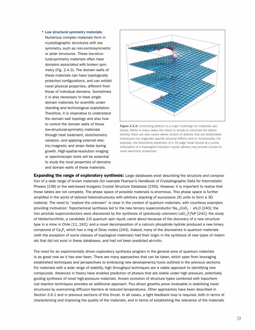
73
• Low structural symmetry materials:
Numerous complex materials form incrystallographic structures with lowsymmetry, such as non-centrosymmetricor polar structures. These low-struc-tural-symmetry materials often havedomains associated with broken sym-metry (Fig. 2.4.3). The domain walls ofthese materials can have topologicallyprotected configurations, and can exhibitnovel physical properties, different fromthose of individual domains. Sometimesit is also necessary to have singledomain materials for scientific under-standing and technological exploitation.Therefore, it is imperative to understandthe domain wall topology and also howto control the domain walls of theselow-structural-symmetry materialsthrough heat treatment, stoichiometryvariation, and applying external elec-tric/magnetic and strain fields duringgrowth. High-spatial-resolution imagingor spectroscopic tools will be essentialto study the local properties of domainsand domain walls of these materials.
Expanding the range of exploratory synthesis: Large databases exist describing the structure and composi-tion of a wide range of known materials (for example Pearson’s Handbook of Crystallographic Data for Intermetallic Phases [238] or the web-based Inorganic Crystal Structure Database [239]). However, it is important to realize that these tables are not complete. The phase space of possible materials is enormous. This phase space is further amplified in the world of tailored heterostructures with arbitrary stacking of successive 2D units to form a 3D material. The need to “explore the unknown” is clear in the context of quantum materials, with countless examples providing motivation: Topochemical synthesis led to the new ternary superconductor Na0.3CoO2 • xH2O [240]; the iron pnictide superconductors were discovered by the synthesis of (previously unknown) LaO1-xFxFeP [241]; the study of Herbertsmithite, a candidate 2-D quantum spin liquid, came about because of the discovery of a new structure type in a mine in Chile [11, 242]; and a novel decomposition of a calcium phosphide hydride produced a new binary compound of Ca3P2 which has a ring of Dirac nodes [243]. Indeed, many of the discoveries in quantum materials (with the exception of some classes of topological materials) had their origin in the synthesis of new types of materi-als that did not exist in these databases, and had not been predicted ab-initio.
The need for an experimentally driven exploratory synthesis program in the general area of quantum materials is as great now as it has ever been. There are many approaches that can be taken, which span from leveraging established techniques and perspectives to embracing new developments/tools outlined in the previous sections. For materials with a wide range of stability, high throughput techniques are a viable approach to identifying new compounds. Advances in theory have enabled prediction of phases that are stable under high pressure, potentially guiding synthesis of novel high-pressure materials. Known evolution of structure types combined with topochem-ical reaction techniques provides an additional approach. Flux driven growths prove invaluable in stabilizing novel structures by overcoming diffusion barriers at reduced temperatures. Other approaches have been described in Section 3.6.1 and in previous sections of this thrust. In all cases, a tight feedback loop is required, both in terms of characterizing and improving the quality of the materials, and in terms of establishing the relevance of the materials
Figure 2.4.2: Controlling defects is a major challenge for materials syn-thesis. While in many cases the intent is simply to minimize the defect density, there are also cases where control of defects that are deliberately introduced can engender specific physical effects and/or functionality. For example, the theoretical prediction of a 1D edge mode bound at a screw dislocation of a topological insulator crystal (above) may provide access to novel electronic properties.
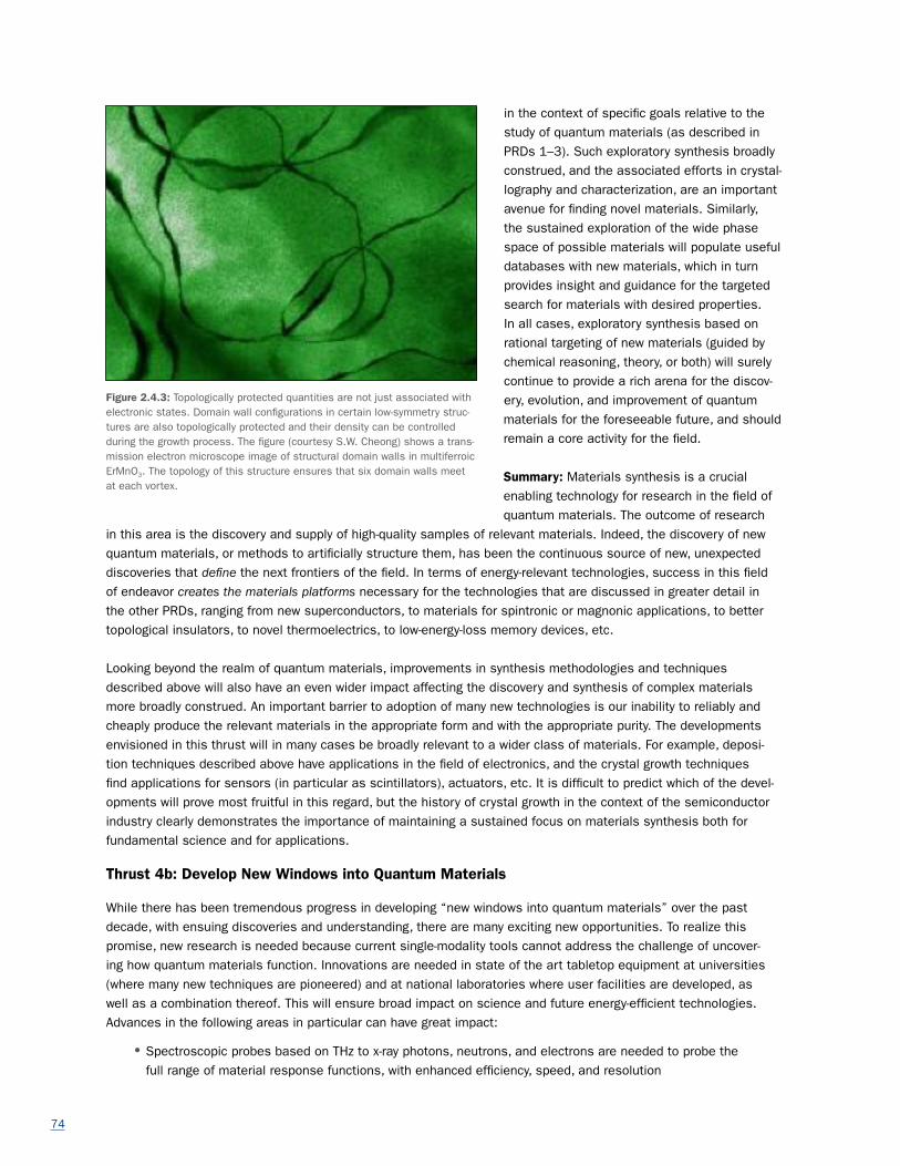
74
in the context of specific goals relative to the study of quantum materials (as described in PRDs 1–3). Such exploratory synthesis broadly construed, and the associated efforts in crystal-lography and characterization, are an important avenue for finding novel materials. Similarly, the sustained exploration of the wide phase space of possible materials will populate useful databases with new materials, which in turn provides insight and guidance for the targeted search for materials with desired properties. In all cases, exploratory synthesis based on rational targeting of new materials (guided by chemical reasoning, theory, or both) will surely continue to provide a rich arena for the discov-ery, evolution, and improvement of quantum materials for the foreseeable future, and should remain a core activity for the field.
Summary: Materials synthesis is a crucial enabling technology for research in the field of quantum materials. The outcome of research
in this area is the discovery and supply of high-quality samples of relevant materials. Indeed, the discovery of new quantum materials, or methods to artificially structure them, has been the continuous source of new, unexpected discoveries that define the next frontiers of the field. In terms of energy-relevant technologies, success in this field of endeavor creates the materials platforms necessary for the technologies that are discussed in greater detail in the other PRDs, ranging from new superconductors, to materials for spintronic or magnonic applications, to better topological insulators, to novel thermoelectrics, to low-energy-loss memory devices, etc.
Looking beyond the realm of quantum materials, improvements in synthesis methodologies and techniques described above will also have an even wider impact affecting the discovery and synthesis of complex materials more broadly construed. An important barrier to adoption of many new technologies is our inability to reliably and cheaply produce the relevant materials in the appropriate form and with the appropriate purity. The developments envisioned in this thrust will in many cases be broadly relevant to a wider class of materials. For example, deposi-tion techniques described above have applications in the field of electronics, and the crystal growth techniques find applications for sensors (in particular as scintillators), actuators, etc. It is difficult to predict which of the devel-opments will prove most fruitful in this regard, but the history of crystal growth in the context of the semiconductor industry clearly demonstrates the importance of maintaining a sustained focus on materials synthesis both for fundamental science and for applications.
Thrust 4b: Develop New Windows into Quantum Materials
While there has been tremendous progress in developing “new windows into quantum materials” over the past decade, with ensuing discoveries and understanding, there are many exciting new opportunities. To realize this promise, new research is needed because current single-modality tools cannot address the challenge of uncover-ing how quantum materials function. Innovations are needed in state of the art tabletop equipment at universities (where many new techniques are pioneered) and at national laboratories where user facilities are developed, as well as a combination thereof. This will ensure broad impact on science and future energy-efficient technologies. Advances in the following areas in particular can have great impact:
• Spectroscopic probes based on THz to x-ray photons, neutrons, and electrons are needed to probe thefull range of material response functions, with enhanced efficiency, speed, and resolution
Figure 2.4.3: Topologically protected quantities are not just associated with electronic states. Domain wall configurations in certain low-symmetry struc-tures are also topologically protected and their density can be controlled during the growth process. The figure (courtesy S.W. Cheong) shows a trans-mission electron microscope image of structural domain walls in multiferroic ErMnO3. The topology of this structure ensures that six domain walls meet at each vortex.

75
• Real-time and real-space imaging acrossbroad length and time scales and withmultiple contrast mechanisms, to cap-ture how quantum materials function
• New hybrid in situ imaging capabilities
• Multi-dimensional spectroscopies fromTHz to multi-keV.
• New tools to probe solid-state quantumentanglement in spin and orbital sectors
• Access to new phases of matter usingextreme electric and magnetic field,stress, and pressure
• x-ray and neutron scattering underextreme electric and magnetic field,stress, and pressure
Research opportunities: Despite all the advances described above, no one technique can simultaneously probe all properties of a functioning quantum material — rather each spectroscopy or imaging technique provides a window into a small part of the electronic or local structural behavior of the material. As a result, many correlations are lost — which are critical for understanding quantum materials. Material properties are defined by elemental and chemical composition, self-organization, and domain and interface formation. Underlying function is the coupling, cooperativity, quantum
entanglement, and competition between the elementary excitations in the medium (electronic, spin, and vibrational) with charge and energy transfer on intermolecular length scales and across nano-interfaces, and dynamics spanning from the few femtoseconds to seconds and even longer time scales.
To enable new and better windows into quantum materials, the following instrumentation research areas look partic-ularly exciting to pursue:
• Real-time quantum microscope to visualize, manipulate, and control quantum materials, and toprobe entanglement
• Advanced photon, electron, and neutron probes, including hybrid probes
• Probes of quantum materials while they are subjected to extreme environments
• Big Data: Better algorithms and data sharing approaches
Real-time quantum microscope to visualize, manipulate, and control quantum materials: The inherent hetero-geneity and multiple phases present in quantum materials demand a new and powerful set of hyper-spectral and multifunctional microscopies. Indeed, this may be the only way to obtain a complete understanding of the underlying complex physics of quantum materials and unlock their technological potential. For example, in phase transitions in quantum materials, no experiment to date has resolved both the collective electronic transition as well as the associated structural phase transition. This capability demands a combination of different techniques (broadband photons, neutrons, electrons, muons, etc.) that can probe the coupled dynamic electronic and lattice motions over multiple length and time scales (Å and attoseconds on up). Such experiments may also uncover routes for access-ing new states of quantum matter.
Figure 2.4.4: New coherent x-ray beams for probing quantum materials.(Top) Coherent x-ray beams from the Linac Coherent Light Source (LCLS) x-ray free electron laser (XFEL) can probe how spins on different atomic sitesbehave. (Bottom) The new quantum coherent high harmonic light source can generate linearly and circularly polarized soft x-rays, to probe the fastest coupled charge and spin dynamics in magnetic materials.
$101 MAY 2015 sciencemag.org
Climate change threatens one in six species pp. 501 & 571
Precision medicine for psychiatry p. 499
The game show where science wins big p. 493
FRONTIERS IN LIGHT AND OPTICS
SPECIAL ISSUE

76
For a comprehensive view of competing phases in a quantum material, it is necessary to systematically enhance and in certain cases combine x-ray, electron, neutron, muon, STM, and nano-optical probes on the same sample or set of samples, taking advantage of their individual capabilities to probe different aspects of the material and its order parameters. Yttrium barium copper oxide (YBCO) is a case in point where a broad range of experimental techniques and thirty years of work were needed to obtain the present overview of the electronic phase diagram (Fig. 3.1.1 and 3.1.2). Even so we are far from a comprehensive understanding of the phase diagram. Accelerated progress on new quantum materials as they emerge from enhanced efforts in synthesis may be achieved through co-analysis of data from multiple probes and multimodal instrumentation that probe simultaneously in real and reciprocal space with different sensitivities.
Questions that can be addressed include: How are the underlying competing electronic, lattice, strain, and spin parameters coupled to characteristic length scales, texture, and topology in distinct quantum phases? What deter-mines multiple phase coexistence through hierarchies of length scales? Which of the structural heterogeneities are intrinsic to the nature of the quantum phase and which are extrinsic? What are the mechanisms of quantum phase transitions and how can we control them for applications? Can we develop a fundamental understanding of mag-netic or spintronic materials and determine the ultimate speed limit? Can we accelerate the discovery, refinement, and application of new quantum materials with better imaging techniques? Exciting capabilities that can help answer such questions include:
• Fast, real-time nanoscopes as well as hybrid, electron-x-ray-optical spectro-microscopies that can beused to visualize quantum materials from the atomic to multi-domain length scales, and from femto-second time scales on up. Also, new imaging capabilities that can simultaneously capture multiple cor-related properties of a quantum material — electronic, structural, magnetic, mechanical, and transport— in real time 3D for the visualization of the correlations underlying function in quantum materials.
• Tools to probe the range and topology of the underlying quantum entanglement of quantum materials:Though it is apparent that entanglement is an important feature of quantum materials, no experimen-tal method is currently available to probe entanglement. Innovative new methods perhaps involvingentangled photons, entangled neutrons, or quantum coherent light sources are needed.
• Inelastic electron energy loss spectroscopy (EELS) for the study of the charge dynamic structure factor,S(q,w), at meV energy scales: This quantity encodes the dynamics of the collective charge excitations.Amazingly, there is no current technique capable of measuring this quantity with momentum resolutionat the required energy resolution of 1 meV. With better EELS, we will be able to detect and understandthe low-energy charge response functions of quantum materials, laying a foundation for the develop-ment of future many-body theory.
Advanced photon, electron, and neutron probes: instrumentation and methods: X-ray probes: It is just becoming possible to generate coherent light spanning the entire electromagnetic spectrum from the THz to the infrared (IR), visible, UV, extreme ultraviolet (EUV), and x-ray regions, that emerges as perfectly synchronized bursts of radiation, with controlled color, polarization, and linewidth. Free-electron lasers (XFELs) and tabletop high harmonic (HHG) sources produce pulses fast enough to capture all dynamics relevant to function in quantum matter, even at the level of electrons. Hyperspectral ultra-fast light sources from the THz to the x-ray region can probe and control mate-rials transformations by coherently manipulating the charge, spin, and lattice dynamics. The next-generation electro-magnetic waveform generators spanning the THz to the x-ray region should have adjustable temporal coherence (i.e., bandwidth). These include high repetition rate UV and EUV lasers with controlled bandwidth (meV to eV) for coherent imaging, angle-resolved photoemission and quantum coherent spectroscopies, and magnetic spectroscopies.
Neutron scattering: Neutron scattering is an essential probe of quantum materials that has come a long way in the past decade as a result of the spallation neutron source, which provides a range of high throughput instrumentation addressing relevant length and time scales. However, neutron scattering instrumentation able to probe all relevant aspects of quantum materials with greater efficiency and a broader range of thermodynamic parameters is needed:

77
• Broadband high efficiency inelastic neutron scattering that can provide detailed and comprehensive mapping of spin-resolved electronic correlations in small single crystalline samples (<1 mm3) from mK to 1000 K.
• Ultra-high magnetic field neutron scattering instrumentation to probe magnetic structures and exci-tations in states of matter that are only accessible at high fields and to enrich our understanding of lower field states. Examples include accessing the field driven plateau phases of quantum magnets such as SrCu2(BO3)2 [246], probing metamagnetic phase transitions and inter-landau level excitations in strongly-correlated electron systems, probing vortex matter at high fields, and splitting or even driv-ing to zero energy the superconducting spin resonance in high-Tc superconductors [247].
• Ultra-high efficiency and high-resolution powder neutron diffraction for magnetic and chemical structure covering a full range of thermodynamic conditions as a rapid turn-around mail-in service with semi-au-tomatic structural refinement.
• Innovative new polarized beam instrumentation to directly probe quantum entanglement.
• Instrumentation to probe quantum materials driven beyond thermodynamic equilibrium by a wide range of perturbations.
Angle-resolved photoemission spectroscopy: There are major opportunities for angle-resolved photoemission spec-troscopy to probe quantum numbers beyond the energy and momentum of electrons. Major advances in detector technologies with spin polarimetry based on exchange (versus conventional Mott) scattering detectors can pro-vide many orders-of-magnitude improvement in figures of merit such as energy resolution and detection efficiency [248]. This should push spin-resolved ARPES from a specialized to a mainstream technique. Current time-resolved, pump-probe ARPES have been almost exclusively limited in the pump (1.5 eV) and probe (6 eV) energies available. However, advances in laser instrumentation and higher harmonic generation should make it possible to selectively pump distinct collective modes (e.g., in the THz). Such advances will also provide higher photon energies to probe the complete Brillouin zone and energy dispersion of a wide range of quantum materials. In addition to pushing ARPES further into the spin and time domains, instrumentation to investigate a wider range of materials beyond bulk single crystals is needed. Small spot (sub-micron) ARPES is needed to probe heterogeneous samples, such as polycrystalline materials or deliberately fabricated structures (e.g., micron-scale vertical or lateral heterostructures of 2D CDW materials) [245]. The integration of ARPES with state of the art synthesis thin film techniques (e.g., MBE or PLD) has the potential to develop into a versatile probe of emergent quantum matter that can only be realized in monolayer or ultrathin material systems that are unstable outside of a vacuum (e.g., enhancement of high-tempera-ture superconductivity in monolayer FeSe thin films on SrTiO3 [244].)
Scanning probe imaging: Currently, understanding the mechanical and transport properties of materials at the nanoscale using visible lasers is challenging because they are not sensitive to deep nanoscale properties, which can be surprisingly different from those of bulk materials.
Figure 2.4.5: New opportunities for ARPES. (right) Integrate ARPES with synthesis techniques to interrogate fragile or ultrathin quantum materials such as a monolayer of FeSe on SrTiO3. (left) Capture band structure of heterogeneous materials using nano-ARPES with sub- micron spot size.
0.00
–0.10
–0.20
–0.30
0
–1
–2
–3
–4
–5
–6
kll (Å-1) kpar (Å
-1)–0.50 M 0.50
E–E F (
eV)
E–E F (
eV)
1.0 2.0
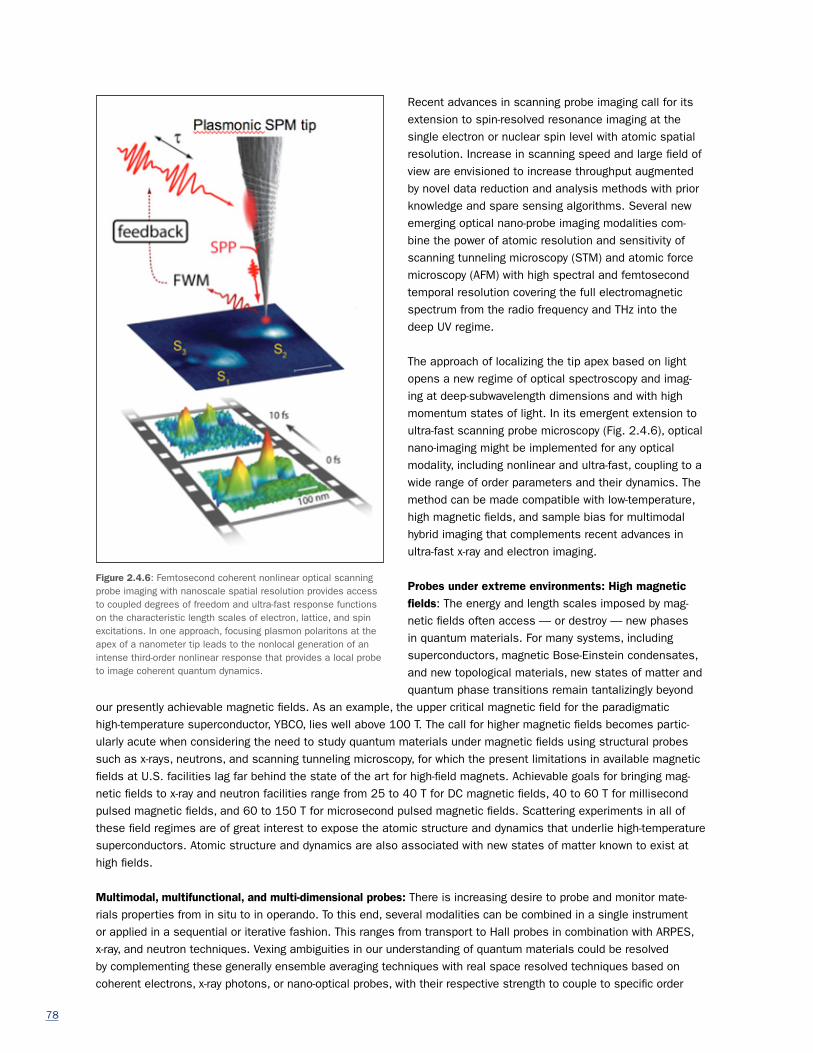
78
Recent advances in scanning probe imaging call for its extension to spin-resolved resonance imaging at the single electron or nuclear spin level with atomic spatial resolution. Increase in scanning speed and large field of view are envisioned to increase throughput augmented by novel data reduction and analysis methods with prior knowledge and spare sensing algorithms. Several new emerging optical nano-probe imaging modalities com-bine the power of atomic resolution and sensitivity of scanning tunneling microscopy (STM) and atomic force microscopy (AFM) with high spectral and femtosecond temporal resolution covering the full electromagnetic spectrum from the radio frequency and THz into the deep UV regime.
The approach of localizing the tip apex based on light opens a new regime of optical spectroscopy and imag-ing at deep-subwavelength dimensions and with high momentum states of light. In its emergent extension to ultra-fast scanning probe microscopy (Fig. 2.4.6), optical nano-imaging might be implemented for any optical modality, including nonlinear and ultra-fast, coupling to a wide range of order parameters and their dynamics. The method can be made compatible with low-temperature, high magnetic fields, and sample bias for multimodal hybrid imaging that complements recent advances in ultra-fast x-ray and electron imaging.
Probes under extreme environments: High magnetic fields: The energy and length scales imposed by mag-netic fields often access — or destroy — new phases in quantum materials. For many systems, including superconductors, magnetic Bose-Einstein condensates, and new topological materials, new states of matter and quantum phase transitions remain tantalizingly beyond
our presently achievable magnetic fields. As an example, the upper critical magnetic field for the paradigmatic high-temperature superconductor, YBCO, lies well above 100 T. The call for higher magnetic fields becomes partic-ularly acute when considering the need to study quantum materials under magnetic fields using structural probes such as x-rays, neutrons, and scanning tunneling microscopy, for which the present limitations in available magnetic fields at U.S. facilities lag far behind the state of the art for high-field magnets. Achievable goals for bringing mag-netic fields to x-ray and neutron facilities range from 25 to 40 T for DC magnetic fields, 40 to 60 T for millisecond pulsed magnetic fields, and 60 to 150 T for microsecond pulsed magnetic fields. Scattering experiments in all of these field regimes are of great interest to expose the atomic structure and dynamics that underlie high-temperature superconductors. Atomic structure and dynamics are also associated with new states of matter known to exist at high fields.
Multimodal, multifunctional, and multi-dimensional probes: There is increasing desire to probe and monitor mate-rials properties from in situ to in operando. To this end, several modalities can be combined in a single instrument or applied in a sequential or iterative fashion. This ranges from transport to Hall probes in combination with ARPES, x-ray, and neutron techniques. Vexing ambiguities in our understanding of quantum materials could be resolvedby complementing these generally ensemble averaging techniques with real space resolved techniques based oncoherent electrons, x-ray photons, or nano-optical probes, with their respective strength to couple to specific order
Figure 2.4.6: Femtosecond coherent nonlinear optical scanning probe imaging with nanoscale spatial resolution provides access to coupled degrees of freedom and ultra-fast response functions on the characteristic length scales of electron, lattice, and spin excitations. In one approach, focusing plasmon polaritons at the apex of a nanometer tip leads to the nonlocal generation of an intense third-order nonlinear response that provides a local probe to image coherent quantum dynamics.
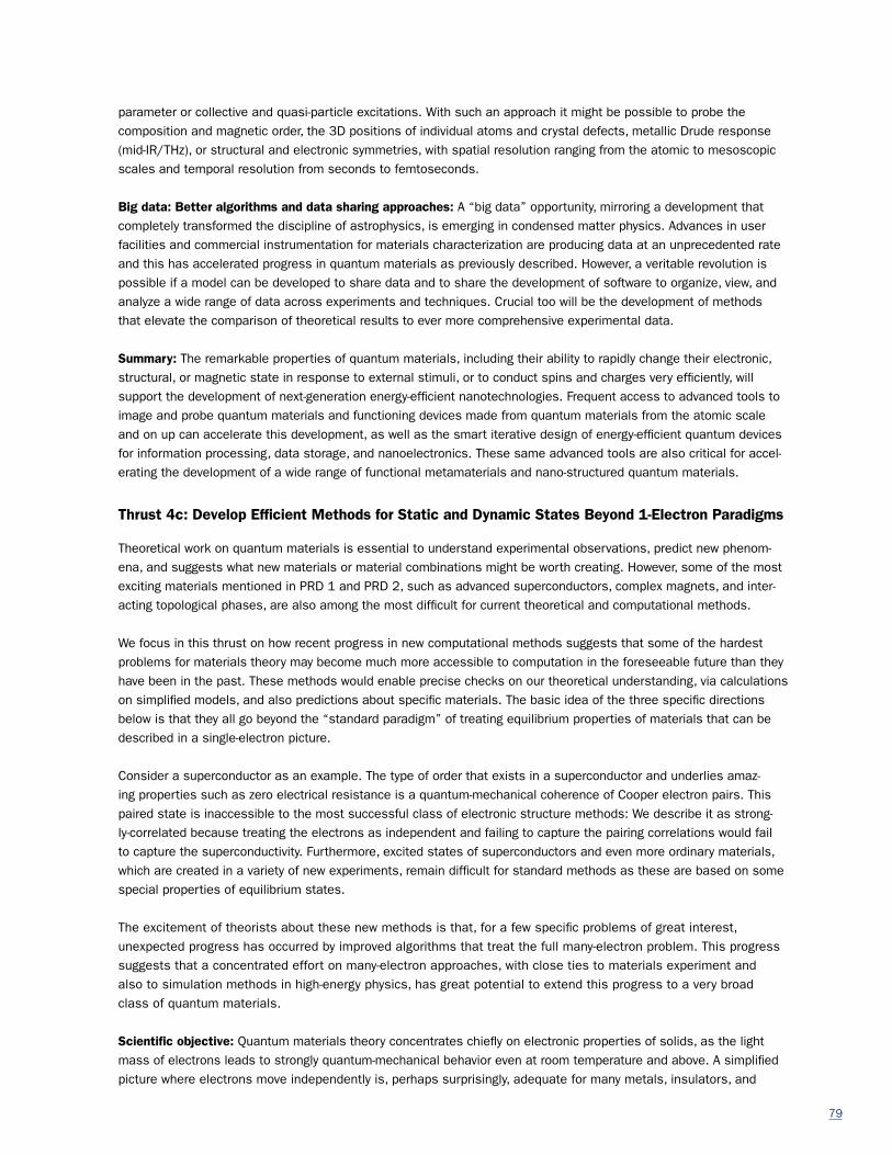
79
parameter or collective and quasi-particle excitations. With such an approach it might be possible to probe the composition and magnetic order, the 3D positions of individual atoms and crystal defects, metallic Drude response (mid-IR/THz), or structural and electronic symmetries, with spatial resolution ranging from the atomic to mesoscopic scales and temporal resolution from seconds to femtoseconds.
Big data: Better algorithms and data sharing approaches: A “big data” opportunity, mirroring a development that completely transformed the discipline of astrophysics, is emerging in condensed matter physics. Advances in user facilities and commercial instrumentation for materials characterization are producing data at an unprecedented rate and this has accelerated progress in quantum materials as previously described. However, a veritable revolution is possible if a model can be developed to share data and to share the development of software to organize, view, and analyze a wide range of data across experiments and techniques. Crucial too will be the development of methods that elevate the comparison of theoretical results to ever more comprehensive experimental data.
Summary: The remarkable properties of quantum materials, including their ability to rapidly change their electronic, structural, or magnetic state in response to external stimuli, or to conduct spins and charges very efficiently, will support the development of next-generation energy-efficient nanotechnologies. Frequent access to advanced tools to image and probe quantum materials and functioning devices made from quantum materials from the atomic scale and on up can accelerate this development, as well as the smart iterative design of energy-efficient quantum devices for information processing, data storage, and nanoelectronics. These same advanced tools are also critical for accel-erating the development of a wide range of functional metamaterials and nano-structured quantum materials.
Thrust 4c: Develop Efficient Methods for Static and Dynamic States Beyond 1-Electron Paradigms
Theoretical work on quantum materials is essential to understand experimental observations, predict new phenom-ena, and suggests what new materials or material combinations might be worth creating. However, some of the most exciting materials mentioned in PRD 1 and PRD 2, such as advanced superconductors, complex magnets, and inter-acting topological phases, are also among the most difficult for current theoretical and computational methods.
We focus in this thrust on how recent progress in new computational methods suggests that some of the hardest problems for materials theory may become much more accessible to computation in the foreseeable future than they have been in the past. These methods would enable precise checks on our theoretical understanding, via calculations on simplified models, and also predictions about specific materials. The basic idea of the three specific directions below is that they all go beyond the “standard paradigm” of treating equilibrium properties of materials that can be described in a single-electron picture.
Consider a superconductor as an example. The type of order that exists in a superconductor and underlies amaz-ing properties such as zero electrical resistance is a quantum-mechanical coherence of Cooper electron pairs. This paired state is inaccessible to the most successful class of electronic structure methods: We describe it as strong-ly-correlated because treating the electrons as independent and failing to capture the pairing correlations would fail to capture the superconductivity. Furthermore, excited states of superconductors and even more ordinary materials, which are created in a variety of new experiments, remain difficult for standard methods as these are based on some special properties of equilibrium states.
The excitement of theorists about these new methods is that, for a few specific problems of great interest, unexpected progress has occurred by improved algorithms that treat the full many-electron problem. This progress suggests that a concentrated effort on many-electron approaches, with close ties to materials experiment and also to simulation methods in high-energy physics, has great potential to extend this progress to a very broad class of quantum materials.
Scientific objective: Quantum materials theory concentrates chiefly on electronic properties of solids, as the light mass of electrons leads to strongly quantum-mechanical behavior even at room temperature and above. A simplified picture where electrons move independently is, perhaps surprisingly, adequate for many metals, insulators, and

80
semiconductors, but it breaks down in strongly-correlated materials. A classic example is superconductivity as mentioned above; other examples are Mott insulators where the insulating behavior results from repulsive interac-tions between the electrons, and many kinds of magnetic and topological states as described earlier in PRD 1 and PRD 2.
The goal of this thrust is to advance our ability to calculate important properties of strongly-correlated materials, with an eye toward improving and controlling those properties in the future. Hence it is about needed theoretical methodologies for answering questions about the nature of complex superconductors and magnets, correlated topo-logical phases, etc. Many, if not most, of the scientific challenges in the earlier PRDs would benefit from improved theories of many-electron states. These would complement existing DOE theoretical work on methods such as den-sity functional theory (DFT) and improvements like dynamical mean-field theory (DMFT). Such all-electron methods as DFT would in any event be required for a first pass at a complex material, in order to isolate which orbitals require more sophisticated methods.
We can summarize the current state of our ability to calculate materials properties as follows: For properties of materials in or close to thermal equilibrium, theory is quite successful in many cases even if interactions are strong as long as the basic nature of the state does not change too much (for example, there is no “phase transition” between the actual material and a simplified, non-interacting version). In states driven far from thermal equilibrium, as created, for example, by intense laser pumping, even simple materials are very challenging to describe. Such far-from-equilibrium physics is currently topical because new experimental techniques create a variety of controlled far-from-equilibrium excited states. Our ability to extract useful information from such experiments is limited by the current state of theory.
Returning to equilibrium, when the interactions are strong and many-particle effects are important, it is sometimes possible to treat the quantum correlations by mapping the system to a classical statistical problem of interacting particles, and then applying the famous Monte Carlo statistical algorithm to that classical problem. Sophisticated versions of this quantum Monte Carlo approach are widely used for quantum many-particle systems in other fields, such as atomic and high-energy physics. However, in general this mapping runs into a difficulty: The quantum nature of the actual correlations is manifested in a “sign problem” in the Monte Carlo simulation of fermions which greatly limits its accuracy. The second research direction below is in large part about finding new ways to avoid this sign problem in specific correlated models relevant to high-temperature superconductors and other key scientific problems.
However, another class of algorithms, based on “tensor networks,” has made great progress even on cases where quantum Monte Carlo is unworkable because of a sign problem. These can give essentially exact numerical solu-tions of several important problems that were previously unapproachable. Their main impact to date has been on special cases (particularly materials with one- or two-dimensional structure), where they have been decisive in under-standing the static and dynamic properties of several important materials.
Tensor networks: Determining the complicated zero-temperature phase diagrams of quantum materials, which often exhibit many competing phases with very small energy differences, requires powerful and accurate numerical methods. Tensor networks are a rapidly developing class of computational approaches that can treat many systems that quantum Monte Carlo cannot, particularly doped fermion systems and frustrated magnetic systems [97, 250]. Furthermore, tensor networks provide a new framework for understanding quantum systems with important theoreti-cal uses independent of how such systems are used in simulations.
The first broadly successful tensor network approach was the density matrix renormalization group (DMRG). Developed in 1992, DMRG became and is still the most powerful method for 1D systems, where it can determine both static and dynamic properties with high accuracy [98]. The broader field of tensor networks began to emerge around 2000, as deep connections between quantum information and DMRG were discovered [251]. We now under-stand DMRG and tensor networks as natural low entanglement approximations. One of the most important proper-ties of quantum ground states of typical physical systems is their low entanglement. This is described by the Area

81
Law which states that the entanglement entropy of a ground state with respect to a bipartition scales as the area of the cut dividing the system, rather than the volume. In the 1D case the Area Law naturally leads to a matrix product state representation of the wave-function, which underlies DMRG.
This deeper understanding has led to very rapid advances since 2000. Two developments in simulations have been particularly important. First, DMRG methods applied to 2D, particularly for frustrated magnets, have steadily improved and reach the point where many ground state phase diagrams can be determined with high reliability, extrapolated to the thermodynamic limit — in spite of a calculation time that grows exponentially with the width of the system. For example, studies of the Heisenberg model on the Kagomé lattice on cylindrical clusters with widths up to 12 sites provided convincing evidence in 2011 that the ground state of the Kagomé lattice is a spin liquid — a problem that had been studied without resolution since the early 1990s [55]. Second, tensor networks specifically adapted for higher dimensions were developed, such as projected entangled pair states (PEPS) as described in Fig. 2.4.7. PEPS has been applied with impressive results to fermion systems, such as the 2D t-J model [252] and to frustrated magnetic systems, such as the magnetized Shastry-Sutherland model [253]. PEPS can work directly in the thermodynamic limit, eliminating finite size effects, with systematically controlled accuracy.
Tensor network methods are still young and there remains much room for improvement. For example, the calcula-tion time for PEPS grows exponentially with the accuracy-controlling tensor bond dimension; faster algorithms need to be found. Two-dimensional electron systems with a Fermi surface have significant logarithmic corrections to the area law, which are not efficiently described with a PEPS wave-function. Different tensor networks need to be found to treat these systems, and to treat these and other systems with non-Area Law entanglement. Very little work has been done on developing tensor networks for three-dimensional models, but in principle methods such as PEPS may work well in 3D. Dynamical means field theory methods have proven useful for 3D (and 2D) strongly interacting systems for a number of years. Recently, a similar cluster/bath method, density matrix embedding theory, has been developed based on entanglement ideas, which is both very efficient and surprisingly accurate, i.e., nearly as reli-able as PEPS for systems such as the 2D Hubbard model [254]. Given that all current methods still have significant limitations, it has proved fruitful to study systems with several methods simultaneously [255]. When multiple meth-ods using quite different types of approximations agree, one can have much more confidence about the results.
Tensor networks can be used to solve the time-dependent Schrodinger equation, potentially providing important dynamical information for comparing with experiments, but the simulations break down as the entanglement of the state grows in time. Despite this, there have been notable successes in obtaining dynamics in 1D through t-DMRG [256]; these methods need to be transferred to two dimensions. Similarly, methods for studying finite temperature need to be transferred to 2D applications, where, for example, one could address long-standing experimental puz-zles in the cuprates, including the nature of the pseudogap phase and the linear resistivity at optimal doping, and aid in the prediction of new superconductors.
Figure 2.4.7: Examples of different types of tensor networks. A tensor network is a structure for a set of many-particle quantum states that is smaller, and hence easier to work with, than the set of all possible states (the Hilbert space), while still capturing correlations with high accuracy. Depending on the problem at hand, it may be more efficient to use a regular lattice structure (PEPS) or a hierarchical network (multi-scale entanglement renormalization ansatz [MERA]).
PEPS
1D Mera
2D Mera

82
Quantum Monte Carlo simulations: From Hamiltonians to gauge theories: Some of the most challenging prob-lems in quantum matter today are related to spin systems on geometrically frustrated lattices, strongly interacting electrons in a magnetic field and quantum phase transitions that involve restructuring of Fermi surfaces. Quantum Monte Carlo (QMC) methods provide an important tool-set to tackle such difficult problems, and we start by review-ing several currently used methods.
Variational methods start with a proposed trial for many-particle wave-function. By using Monte Carlo based algo-rithms to sample configurations of particles with the largest weights, it is possible to obtain a good estimate of the ground state energy and correlations. The success stories of this method include Feynman’s wave-function for a superfluid, the BCS wave function for a superconductor, Laughlin and Jain’s wave functions for the quantum Hall effect, and the resonating valence bond method for high-Tc superconductors [257]. However, variational methods include a huge element of intuition and bias. Next in complexity, zero temperature projected methods such as Green Function MC or Diffusion MC can project out the many particle ground state from a variational state for bosons that have nodeless wave functions or for fermions if the nodes can be approximated by a known wave function.
However, if we demand algorithms that are unbiased and provide statistically “exact” answers in d-dimensions, the most promising methods are determinantal or auxiliary field QMC methods. By introducing auxiliary fields at each space-time point σ(x,t) in a path integral representation of the partition function, the quartic interaction terms can be factored into quadratic forms. The fermions can now be integrated out yielding a partition function as a sum of determinant ρ over auxiliary field configurations, and it is the negative sign or complex phase of this determinant that is the source of problems in QMC simulations.
Several innovative ideas, with a flavor of “doubling,” have been generated to go around the sign problem, such as utilizing (a) particle-hole symmetry [258], (b) two orbitals [259], and (c) representing the fermion as two Majorana modes [260]. Another promising route has been to expertly design models (“de-signer Hamiltonians”) [261] in which the sign problem is either absent or can be solved.
Simulating lattice gauge theories: While gauge interactions are usually introduced in particle physics by hand, recent developments in condensed matter physics suggest that they may emerge naturally at low energies, at quan-tum critical points in certain models that do not contain any explicit gauge fields at the microscopic level. In these models gauge fields arise due to fractionalization of the microscopic degrees of freedom, and these fractionalized particles carry the gauge charge [262]. Thus, one approach to study the associated physics is to directly simulate
Figure 2.4.8: The microscopic spin Hamiltonian on the frustrated pyrochlore lattice can be described by an effective gauge theory of emergent fractionalized S=±1/2 spinons attached by a string. QMC simulations at the microscopic and effective gauge theory level present different challenges.

83
the Hamiltonian for a frustrated quantum spin system by DMRG methods or by QMC methods. In certain cases the fractionalized degrees of freedom may emerge in the form of local space-time regions that can be used in the QMC [263]. Another approach is to simulate the emergent gauge theory itself, typically U(1) or Z(2), since it may be sim-pler for describing the physics of the fractionalized quasi-particles. See Fig. 2.4.8 for the example of quantum spin ice, which can be described in terms of a gauge theory. The numerical challenges of simulating the gauge theory can be different from those of simulating the microscopic model [264]. Furthermore, the gauge theory can provide important insights into the confined versus deconfined nature of the quasi-particles and their entanglement and topological properties.
Theoretical methods and concepts for quantum materials far from equilibrium: The evolution of driven systems involves a broad class of phenomena that crosses many scientific disciplines, as the world around us is far from being in static equilibrium. It continually evolves to exhibit a myriad of far-from-equilibrium behaviors as systems respond to external stimuli. This governs broadly important behaviors, such as plant production of glucose and oxygen in response to sunlight and CO2, the classical analog for the development of complex weather systems in response to warm air and moisture currents, and the volatile evolution of financial markets in response to economic stimuli. Thus the study of non-equilibrium behavior underlies many of the DOE Grand Challenges and involves a broad class of phenomena that crosses many scientific disciplines.
The goal of ultra-fast materials science studies is to understand and potentially control emergent phenomena at their natural time and length scales, under equilibrium and/or extreme conditions. This requires harnessing an understanding of how quantum mechanics plays out at nano- to microscopic length scales and atto- to femto-second time scales, and how it connects to emergent phenomena on mesoscopic scales. This will enable the design and optimization of new materials with desirable properties for energy and other technological applications. This may be accomplished through the use of high-resolution x-ray scattering and spectroscopy using frequency domain and ultra-fast pump-probe time-domain techniques, combined with the development of a variety of theoretical approaches to non-equilibrium situations. This work focuses not only on scientific questions surrounding the origin of emergence but also upon the ability to control the development of novel properties in materials for energy relevant applications. Therefore this research has had and will continue to have an impact in a variety of fields, resulting in substantial advances of great benefit to DOE.
It is clear that in order to describe non-equilibrium behavior and the path towards emergence in complex materials, a more precise and correct vocabulary is needed. The field of far-from-equilibrium physics is extremely broad yet frag-mented into subfields (such as turbulence in fluids, ionization in atomic physics, fracture propagation in solids, and order parameter dynamics in correlated materials) so there is great value in identifying classes of systems that might have common underlying physics or that might be tackled by common methods. This provides important connections to a wide range of other fields, both within and outside physics, and drives the need for attacking ever-bigger and broader problems in far-from-equilibrium phenomena.
With advances in instrumentation and new experimental techniques, parallel theoretical developments are critical for providing a rational basis for experimentation so that resources can be directed to the most promising regions of an exponentially increasing experimental phase space. Advanced light sources based on synchrotron radiation (SSRL, NSLS-II, APS, and ALS) and free electron laser sources (LCLS and LCLS-II [under construction]) enable revolutionary new possibilities for probing matter across multiple length and time scales. Efforts are underway to bring applied mathematics and computer science approaches to the large-scale problem of efficient data handling required to process the large volumes of data generated from these light sources. These efforts include the new Center for Advanced Mathematics for Energy Research Applications (CAMERA) project at LBNL. Without synergy between theory and experiment, it will not be possible to exploit the full potential of powerful, high-throughput, high-resolution modern instrumentation, or to develop new, efficient paradigms for unlocking the workings of novel materials and phenomena.
An example of recent advances is the creation of new states of matter in e.g., topological insulators or transition metal dichalcogenides, through the application of strong electromagnetic fields. A main focus is on the use of circularly polarized light pulses to engineer electronic and structural responses, to combined dynamical breaking of
84
sublattice and time-reversal symmetries. This research provides a rich playground to explore the interplay of non-triv-ial quantum geometry with transport and optical measurements on one hand, while on the other hand serving to establish a firm theoretical and experimental basis to design and access practical valleytronics or optical-switching phase change materials.
The dynamics of superconductors is a field of study with a long, rich history. Until recently, studies were mainly lim-ited to the frequency domain, where measurements are averaged over long times. This changed with the advent of time-resolved spectroscopy, which is performed by exciting the system with an ultra-short pump laser pulse, followed by an equally short probe pulse. These tools have opened a new window into the complex dynamics of supercon-ductors (as well as other ordered phases, e.g., CDW insulators [265]) by performing studies on the gap [266, 267], collective [268], quasiparticle [269, 270], and interaction dynamics [271–274].
In addition to methods that focus on low dimensional materials, nonequilibrium dynamical mean-field theory approaches the problem from the limit of large spatial dimensions. Developed a decade ago [275, 276], nonequilib-rium dynamical mean-field theory has been applied to numerous pump/probe experiments that study how quantum materials relax after they are excited by powerful lasers. The method works particularly well in situations where the many-body physics is dominated by so-called local physics, which takes place when two electrons interact on the same lattice site. In the future, these methods need to be extended to treat real materials (similar to equilibrium density functional theory-dynamical mean-field theory methods employed today), and better methods need to be developed to solve these problems at long times to examine how steady states and metastable nonequilibrium phases form. This will also allow theory to model ultra-fast switching and other technologically relevant phenomena.
Summary: One of several reasons why quantum materials have not yet achieved as broad a technological impact as ordinary semiconductors like silicon is that our understanding of many important phenomena, such as superconduc-tivity, is not highly predictive: Historically it has been difficult to predict in advance which correlated materials will be superconductors, for example, although once a material is known to be superconducting, theory connects that obser-vation to many other properties. Improved theories of quantum materials via the directions described are needed to accelerate the development of quantum materials and achieve the energy applications covered in PRDs 1–3.
Another example of the potential for scientific impact is shown by successful theoretical predictions of one-electron topological materials, where it is now possible to search systematically for candidate materials using high-through-put electronic structure methods. If we understood how to compute many-electron materials with comparable accuracy, then this could be integrated with the Materials Genome Initiative searches to find better superconductors, magnets, etc. This would require not just improved strong correlation methods as described here, but also better ways of extracting the key orbitals and interactions starting from density functional theory or another computation-ally efficient method for relatively weak correlations.

85
3. Basic Research in Quantum Materialsfor Energy Relevant Technology
The Basic Research Needs Workshop on Quantum Materials for Energy-relevant Technology was
structured around five panels and three crosscutting themes:
Superconductivity and Charge Order in Quantum Materials (Section 3.1, Panel 1)
Magnetism in Quantum Materials (Section 3.2, Panel 2)
Transport and Non-Equilibrium Dynamics in Quantum Materialss (Section 3.3, Panel 3)
Topological Quantum Materials (Section 3.4, Panel 4)
Heterogeneous and Nano-Structured Quantum Materials (Section 3.5, Panel 5)
Cross-Cutting Themes (Section 3.6):
1. Materials Synthesis
2. Instrumentation
3. Theory and Modeling
Each panel produced a report on the status of the field, specifically identifying (a) current status and recent advances, (b) scientific challenges and opportunities, and (c) the potential for energy-relevant technologies. These reports (Sections 3.1 through 3.6 of this chapter) provided the basis for identifying the four Priority Research Directions, which are described in Chapter 2.
86
3.1 SUPERCONDUCTIVITY AND CHARGE ORDER IN QUANTUM MATERIALS
Classes of order associated with the charge-sector include charge order; orbital order; valence instabilities and
valence disproportionation; charge density waves (CDW); ferroelectric order; nematic/quadrupolar/octupolar
order; and unconventional superconductivity broadly construed. Competing effects, resulting in frustrated inter-
actions, have been argued to play an important role in several materials. In many cases, deep questions revolve
around the relation between the ordered states, their fluctuations, and superconductivity, especially in the con-
text of associated quantum phase transitions. In all cases, the role played by the inevitable presence of disorder
raises serious theoretical and experimental questions; indeed, a paradigmatic quantum phase transition, still
incompletely understood, is that of the superconductor-to-insulator transition in disordered materials.
3.1.1 Current Status and Recent Advances
Exotic, non-BCS superconductivity has been observed in a variety of complex materials, from heavy-fermions to high-critical-temperature copper- and iron-based compounds. The unifying characteristics of the non-BCS superconductors are (i) strong short-range Coulomb repulsion between conduction electrons, (ii) the simultaneous active role of several degrees of freedom such as charge, spin, orbital, and lattice, and (iii) the effects of disorder introduced by the electronicdoping that in most cases is necessary to inducesuperconductivity.
The competition between Coulomb repulsion and kinetic energy, which respectively favor electronic localization and delocalization, leads to a large variety of emergent orders and to very rich phase diagrams.
Depending on intrinsic properties, such as ionic size, lattice geometry, electronic valence, number of partially filled orbitals, local atomic magnetization, and level of doping, a variety of ground states are stabilized (Fig. 3.1.1) that may be tuned with pressure, magnetic field, etc. These phases are characterized by order parameters that may involve several degrees of freedom. In addition, charge homogeneity and/or translational invariance is absent in many of these phases as a result of the interaction of various degrees of freedom or due to the effects of disorder.
It is now 10 years after the Basic Research Needs for Superconductivity report [280]. A prominent scenario recog-nized in that report is the role of competing orders and the appearance of superconductivity at a quantum critical point where the order competing with superconductivity is suppressed. This picture can apply to conventional as well as unconventional superconductors. For example, charge-density-wave order competes with superconductivity in transition-metal dichalcogenides, though the characteristic transition temperatures of the charge order and super-conductivity can differ by orders of magnitude (Fig.3.1.2[A]).
80
60
40
20
0
Mag
netic
Fie
ld (T
)
Tempe
rature
(K)
Doping (p)
Quantum oscillations
Insulatordρ/dT < 0 Metal
dρ/dT > 0
Superconductivity
SuperconductivitySpin order(neutron/μSR)
Charge order + SC(X-ray)
Charge order + SC(NMR)
Charge order(X-ray)
0.06 0.08 0.1 0.12150
50
100
6.43 6.47
H’
∼H
∼H1/2
Figure 3.1.1: Phase diagram for YBa2Cu3O6+δ.
FPO

87
In the last decade, however, new discoveries have revealed a broader range of possibilities. In particular, there was the important discovery of high-temperature superconductivity in iron pnictides and chalcogenides (see the sidebar “Iron Superconductors: Newest Members of the High-Tc Family”). The conduction states in these materials involve essentially all five of the Fe 3d orbitals. Besides superconductivity, spin-density-wave, orbital, charge-density- wave, and nematic orders (see the sidebar “A Nematic Phase of Correlated Electrons?”) have also been observed in these systems. Importantly, the transition temperatures are of similar magnitude.
In cuprates, an increasingly complex phase diagram is emerging with a range of orders that have comparable transition temperatures (Fig. 3.1.2[B]). In particular, theoretical and experimental indications of a pair density wave, involving spatially-modulated superconductivity enmeshed with modulated antiferromagnetism, have motivated the concept of intertwined orders [5]. Here the idea is that two or more orders may actually be able to enhance one another.
Of course, complex interactions between several degrees of freedom and rich novel phases in a variety of non- superconducting materials also lead to remarkable properties such as in the colossal magnetoresistance manganites, with phases characterized by simultaneous charge, magnetic, and orbital order. Rich phase diagrams have also been observed in frustrated magnets and may be present as well in topological insulating materials.
An important aspect of both the manganites and the iron pnictides is their multi-orbital character. Related to this, there is also recent interest in the effect of strong spin-orbit coupling. For example, considerable attention has focused on iridate compounds such as Sr2IrO4, where the Ir ions are believed to be characterized by J=½. Parallels have been drawn with cuprates, where the Cu ions have spin S=½. The role of quantum magnetism for superconduc-tivity has significant overlap with Panel 2. Spin-orbit coupling also appears to be crucial to the superconductivity in single-layer or few-layer transition-metal dichalcogenides, where evidence for an unusual Ising pairing was recently reported. Of course, the studies of superconductivity in ultra-thin films, at interfaces and at surfaces by electrolytic doping, have a large overlap with Panel 5.
Topological superconductors are of recent interest for the purpose of quantum computing. The best examples of topological superconductors are Sr2RuO4 and the B phase of UPt3. There is also work on inducing topological super-conductivity in films deposited on topological insulators. Such work largely fits within the scope of Panel 4.
Figure 3.1.2: (A) Phase diagram of TaS2 under pressure, showing the competition between commensurate charge density wave (CCDW) and nearly-commensurate CDW (NCCDW) states with superconductivity; note that the superconducting transition temperature is scaled up by a factor of 10. (B) Schematic phase diagram of superconducting cuprates, indicating a variety of coexisting states.

88
IRON SUPERCONDUCTORS: NEWEST MEMBERS OF THE HIGH-TC FAMILY
Discovered in 2006, iron-based super-conductors are the newest members of the high-Tc family, as shown in the upper figure. Like the cuprates (copper oxides), iron-based superconductors are complex compounds with a layered structure; the crystal structure of a specific example (BaFe2As2) is shown in the lower figure. The Fe atoms (black) form a square lattice while the As atoms (red) are located above and below the Fe planes at the center of alternate squares. Superconductivity can be induced in these materials by a number of means, including chemical substi-tution and hydrostatic pressure. A photograph of a crystal of Co-doped BaFe2As2 is shown in the right panel of the lower figure.
An important difference between cuprates and iron-based superconductors is that the undoped cuprates are insulators due to strong interactions between the electrons, while the undoped iron-based materials are poor metals. In addition, each copper (Cu) atom in the cuprates contributes only a single electron to the conduction states, whereas each Fe atom in the iron-based superconductors contributes electrons from all five of its atomic-like 3D orbitals. The discovery of the iron-based superconductors has added a new piece to the puzzle of high-Tc superconductivity and introduced the need to develop novel experimental and theoretical techniques to handle the orbital degrees of freedom that may play a role in the electron-pairing mechanism of these materials.
140
120
100
80
60
40
20
1900 1920 1940 1960 1980 2000 2020
(Year)
Tc(K
)
HgPb Nb
NbN Nb3Sn
YBa2Cu3O7
(La, Ba)2CuO4
HgBa2Ca2Cu3Ox
Tl2Ba2Ca2Cu3Ox
Bi2Sr2Ca2Cu3Ox
Nb3Ge
MgB2
Cs2RbC60
C-basedK3C60
(TMTSF)2PF6
Metal
Cuprates
Fe-basedSmFeAs(O, F)
LaFeAs(O, F)
LaFePO
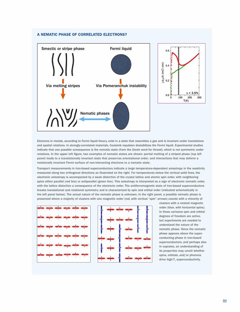
89
A NEMATIC PHASE OF CORRELATED ELECTRONS?
Electrons in metals, according to Fermi liquid theory, exist in a state that resembles a gas and is invariant under translations and spatial rotations. In strongly-correlated materials, Coulomb repulsion destabilizes the Fermi liquid. Experimental studies indicate that one possible consequence is the nematic state (from the Greek word for thread), which is not symmetric under rotations. In the upper left figure, two examples of nematic states are shown: partial melting of a striped phase (top left panel) leads to a translationally invariant state that preserves orientational order; and interactions that may deform a rotationally invariant Fermi surface of non-interacting electrons to a nematic state.
Transport measurements in iron-based superconductors indicate a large temperature-dependent anisotropy in the resistivity measured along two orthogonal directions as illustrated on the right. For temperatures below the vertical solid lines, the electronic anisotropy is accompanied by a weak distortion of the crystal lattice and atomic spin order, with neighboring spins either parallel (red line) or antiparallel (green line). This anisotropy is interpreted as a sign of electronic nematic order, with the lattice distortion a consequence of the electronic order. The antiferromagnetic state of iron-based superconductors breaks translational and rotational symmetry and is characterized by spin and orbital order (indicated schematically in the left panel below). The actual nature of the nematic phase is unknown. In the right panel, a possible nematic phase is presented where a majority of clusters with one magnetic order (red, with vertical “spin” arrows) coexist with a minority of
clusters with a rotated magnetic order (blue, with horizontal spins). In these cartoons spin and orbital degrees of freedom are active, but experiments are needed to understand the nature of the nematic phase. Since the nematic phase appears above the super-conducting phase in iron-based superconductors, and perhaps also in cuprates, an understanding of its properties may unveil whether spins, orbitals, and/or phonons drive high-Tc superconductivity.
Nematic phases
Smectic or stripe phase Fermi liquid
Via Pomeranchuk instabilityVia melting stripes
ρa,ρ
b (m
Ω c
m)
T(K)
0.6
0.4
0.2
0.00 100 200 300
x = 3.5%
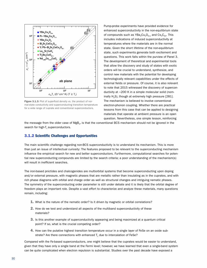
90
Pump-probe experiments have provided evidence for enhanced superconductivity in the non-equilibrium state of compounds such as YBa2Cu3O6+x and Cs3C60. This includes indications of induced superconductivity at temperatures where the materials are in the normal state. Given the short lifetime of the non-equilibrium state, such experiments generate both excitement and questions. This work falls within the purview of Panel 3. The development of theoretical and experimental tools that allow the discovery and study of states with exotic orders will be crucial to understand, synthesize, and control new materials with the potential for developing technologically relevant capabilities under the effects of external fields or pressure. Of course, it is also relevant to note that 2015 witnessed the discovery of supercon-ductivity at ~200 K in a simple molecular solid (nom-inally H3S), though at extremely high pressure [281]. The mechanism is believed to involve conventional electron-phonon coupling. Whether there are practical lessons from this case that can be applied to designing materials that operate at ambient pressure is an open question. Nevertheless, one simple lesson, reinforcing
the message from the older case of MgB2, is that the conventional BCS mechanism should not be ignored in the search for high-Tc superconductors.
3.1.2 Scientific Challenges and Opportunities
The main scientific challenge regarding non-BCS superconductivity is to understand its mechanism. This is more than just an issue of intellectual curiosity: The features proposed to be relevant to the superconducting mechanism influence the empirical search for new and better superconductors. Furthermore, computational searches for poten-tial new superconducting compounds are limited by the search criteria; a poor understanding of the mechanism(s) will result in inefficient searches.
The iron-based pnictides and chalcogenides are multiorbital systems that become superconducting upon doping and/or external pressure, with magnetic phases that are metallic rather than insulating as in the cuprates, and with rich phase diagrams with orbital and charge order as well as structural changes and intriguing nematic phases. The symmetry of the superconducting order parameter is still under debate and it is likely that the orbital degree of freedom plays an important role. Despite a vast effort to characterize and analyze these materials, many questions remain, including:
1. What is the nature of the nematic order? Is it driven by magnetic or orbital correlations?
2. How do we test and understand all aspects of the multiband superconductivity of thesematerials?
3. Is this another example of superconductivity appearing and being maximized at a quantum criticalpoint? If so, what is the crucial competing order?
4. How can the putative highest transition temperature occur in a single layer of FeSe on an oxide sub-strate? Are there connections with enhanced Tc due to intercalation of FeSe?
Compared with the Fe-based superconductors, one might believe that the cuprates would be easier to understand, given that they have only a single band at the Fermi level; however, we have learned that even a single-band system can be quite complicated when electron repulsion is substantial. Studies over the past decade have exposed a
Figure 3.1.3: Plot of superfluid density vs. the product of nor-mal-state conductivity and superconducting transition temperature for a wide range of cuprate and conventional superconductors.
ab plane
109
108
107
109 108 107
σdcTc (Ω-1 cm-1 K) (T ≳ Tc)
𝜌𝜌 s
ω2
pS (
cm-2)
YBa2Cu3O6+x
Pr–YBa2Cu3O7-δ
YBa2Cu4O8
Bi2Sr2CaCu2O8-δ
Y/Pb–Bi2Sr2CaCu2O8-δ
La2-xSrxCuO4
Tl2Ba2CuO6+δ
Nd1.85Ce0.15CuO4

91
phase diagram that is more complex than anticipated. Spin-density-wave, charge-density-wave, and nematic orders are all prominent, and exotic phases such as orbital-loop-current order have been proposed. There are even proposals of states with topological order that is not directly measurable by experiment. We are faced with old and new questions:
1. How do we understand the pseudogap that violates the Fermi liquid model in the normal state?
2. Does precursor pairing occur in the normal state, and is there a unique way to determine this experimentally?
3. How do we understand the emergent Fermi liquid behavior that appears at low temperature and high magnetic field together with CDW order?
As for properties beyond superconductivity, the field is wide open. Can we find other examples where multiple order parameters enhance one another, rather than simply compete? Can we take advantage of competing or intertwined orders to produce materials with other technologically important functionality? Can we find new approaches to thermoelectrics, ferroelectrics or multiferroics? For example, families of compounds related to SnSe and Bi2Se3 are excellent thermoelectrics, but they can also be topological insulators or superconductors. Can these connections be exploited in a useful way? Could one exploit the insulating, charge-ordered states that occur in various electronical-ly-doped correlated insulators to produce extreme responses?
A common feature of many correlated systems is a strong response to local defects and disorder (see the sidebar “Embracing Disorder in Quantum Materials”). Such effects are not adequately accounted for by mean-field theories. There are also cases where disorder effects become apparent in the collective response of materials. For example, Fig. 3.1.3 shows a scaling relation for both cuprate and conventional superconductors, where the common feature appears to be a superconducting coherence length that is limited by impurity scattering. Comparisons have been made to granular superconductors. Reconciling such behavior with theoretical models of pairing is an outstanding challenge.
Disorder and heterogeneity can also be key for optimizing the performance of materials such as superconductors. The critical current — the maximum loss-less current — of a superconductor is determined by the dynamics of superconducting vortices. High critical currents arise when vortices are immobilized or pinned at defects, which introduces heterogeneity into the superconductor (see the sidebar “Embracing Disorder in Quantum Materials”). Effective pinning defects span a wide range of length-scales. They include point defects in the form of atomic vacan-cies or interstitials, non-superconducting precipitates of various sizes and shapes, grain boundaries, stacking faults,
Figure 3.1.4: Measurements of the actual defect distribution in a commercial superconducting wire can be performed by 3D transmis-sion-electron-microscope tomography and used as input to large-scale simulations that can attempt to predict the critical current as a function of magnetic field and temperature.
Commercial HTS 3D TEM tomography of YBCO coated
Simulations of vortex interactionwith a mixed defect landscape
Solder
Metal stabilizer strips
HTS
Buffers
Laminated wire

92
EMBRACING DISORDER IN QUANTUM MATERIALS
The word “disorder” has negative connotations. Theorists tend to focus exclusively on models with perfect order, while crystal growers attempt to minimize defects and disorder. Ignoring disorder, however, does not make it go away nor reduce its impact on physical properties. It is now clear that disorder has profound impacts on strongly-correlated materials and must be addressed by both theory and experiment.
Local defects can generate strong responses. Top figure on the left shows an atomic-resolution image obtained with a scanning tunneling microscope around an atomic vacancy (dark triangle) on the surface of the layered com-pound NbSe2. One can see charge-density-wave (CDW) oscillations (varying light and dark stripes) near the vacancy. CDW order does occur in NbSe2 at low temperature; however, this image was measured well above the CDW transition temperature. Conventional theory has explained CDW order in terms of a weak interaction between electron waves and the crystal lattice. In contrast, the analysis of such images contributes to a growing consen-sus that CDW oscillations in this and related compounds are due to strong interactions between electronic excitations and specific lattice vibrations. The CDW fluctuations present at high temperatures are pinned by impurities. Deliberate introduction of impurities may help to understand phases that are otherwise only stable at lower temperatures, or at extreme pressures or fields.
Another reason to address disorder is that a high density of defects can drive quantum phase transitions, such as from a superconductor to an insulator. The second panel from the top shows a measurement of the single-electron density of states in a disordered InO film, as a function of energy (lower right axis, V) and temperature (lower left axis T); the super-conducting transition temperature is indicated by the dashed line. The pairing of electrons in the superconducting state causes the single-electron density of states to dip to zero at low energy. This dip survives above the transition temperature due to disorder, which destroys the phase coherence of the superconducting state but not electron pairs. The third panel shows a theoretical calculation, taking disorder into account, that yields consistent features. Increasing structural disorder can destroy superconductivity while leaving evidence of localized electronic pairs in the density of states.
Disorder may also play a role in the stabilization of phases such as the nematic phase observed in the iron pnictides upon electron doping via replacement of Fe by a transition metal such as Co in the Fe-As planes. In the bottom panel, unidirectional electronic modulations along the a-axis are revealed by STM in the nematic phase of Co-doped CaFe2As2. Theoretical calculations with the help of computers, including the disorder introduced by doping, show that out-of-phase clusters with short-range (π,0) order are anchored by impurities. The numerically calculated nematic order parameter reproduces the experimental result.
93
dislocations, and strain fields extending over hundreds of nanometers. In ‘real’ samples, typically a mixture of sev-eral of these defects is encountered yielding a complex, mixed-pinning landscape. Furthermore, the combination of pinning interactions, repulsive vortex-vortex interactions and thermally activated dynamics gives rise to exceedingly complex, non-linear, and multi-scale dynamics. Exploring all possible defect landscapes in superconductors in order to find the “best” configuration for the highest possible critical current is experimentally prohibitive. Furthermore, the complex dynamic behavior of vortex matter has proven difficult to capture in analytical models. Modeling the effectiveness of a vortex pinning landscapes is a challenge, and one that can depend on the quality of experimental imaging of defects in real samples, as illustrated in Fig. 3.1.4.
As a result of the challenging problem of characterizing and understanding strongly-correlated electron systems, a broad arsenal of techniques has emerged. On the theoretical side a variety of many-body techniques have been developed. Computer simulations have emerged as a well-established tool to guide the evaluation of physical mech-anisms. The simpler theoretical and computational study of quasi-one dimensional chains and ladders has shed light on the behavior of real strongly-correlated materials. On the experimental side, synthesis leads the way. Recent developments include in situ x-ray diffraction detection of metastable crystalline phases within a furnace, and field-effect doping at the surface of thin films. For sample characterization, we are equipped with techniques such as neutron scattering, angle resolved photoemission spectroscopy, resonant and inelastic x-ray scattering, infrared and THz spectroscopy, scanning tunneling microscopy, and nuclear magnetic resonance (NMR), which provide detailed information on magnetic states, charge order, Fermi surfaces, gap structures, and dynamics.
To support these capabilities, DOE has continued to invest in new infrastructure over the last decade. Supercomputer capabilities have been expanding at a remarkable rate. New and improved light sources provide x-ray beams with enhanced coherence and brightness, as well as very short pulses for pump-probe studies. A powerful new spallation neutron source is up and running.
Specific areas of opportunity include the following:
• Analytical and numerical approaches to handle multi-orbital systems with interacting charge, spin,orbital, and lattice degrees of freedom.
• Theoretical tools to study the effects of disorder due to doping in strongly interacting multi-orbital systems.
• Experimental investigation of “hidden order parameters,” such as nematic and quadrupolar or highermultipole order that result from the interaction/competition of multiple degrees of freedom.
• Atomic scale visualization techniques to study the properties of materials at the nanoscale.
• Rational synthesis of materials with potential functionalities, crystal growth in extreme environments,and realization of field-effect doping.
• Magnetic, charge, and structural properties of materials via neutron, x-ray, and electron scattering,including data analysis techniques that can be applied to inhomogeneous ground states.
• Development of new experimental probes, such as effective electron-energy-loss spectrometers todetermine the bosonic excitation spectrum, and Josephson tunneling microscopes to spatially resolvethe superconducting wave function.
• Optimization of functional properties for technological applications.
• Importance of competing tendencies. Potential to induce non-linear “colossal” effects via externalparameters such as electric and magnetic fields.

94
3.1.3 Potential for Energy-relevant Technologies
The discovery of superconductivity in the cuprates led to incipient technological applications such as wiring in superconducting magnets for particle accelerators and some applications in urban electric grids. The technologi-cal challenges are huge, but the potential pay-off in energy savings make this research worthwhile. While a direct exploitation of the superconducting state seems the most straightforward technological path, the development, understanding, and control of materials in which a superconducting state coexists or competes with multiple other ordered states offers great potential for technological applications that may be relevant in medicine, information, military, and energy technologies:
• Superconducting wires made of high-Tc materials.
• Medical applications: nanoparticles of materials whose properties can be externally controlled can be injected to deliver targeted heat, magnetic fields, etc.
• Electric motors for ship propulsion.
• High power delivered at low DC voltage for data centers and naval vessels.
• High-power transmission lines, especially within cities.
• Fault current limiters and high power interconnects for grid stabilization.
• Magnetic energy storage.
• High-field magnets, especially for magnetic resonance imaging (MRI).
• Josephson junction devices for quantum computing.
• Magnetic levitation for high-speed transportation (“hover trains”).
• Radio frequency (RF) and microwave filters.
• Superconducting quantum interference devices (SQUIDs) for detection of very weak magnetic fields.
In addition, thermoelectrics are excellent for converting waste heat into electricity; practical heat sources include internal combustion engines and solar radiation.
Solids with first order transitions and large entropy gain can be applied to solid-state refrigeration, potentially improving efficiency and reliability and reducing the need for refrigerant chemicals that can be detrimental to the ozone layer.
95
3.2 MAGNETISM IN QUANTUM MATERIALS
Magnetism, in the broadest sense, covers all collective quantum phenomena associated with electronic spin
degrees of freedom. For centuries magnetism has offered deep scientific challenges and provided essential
technical functionalities. Because of the collective character of magnetic phenomena, advances in magnetism
research frequently break new ground in many-body quantum physics. Magnetic order also has many applica-
tions because it breaks time reversal symmetry, yields hysteretic behavior, and is frequently very robust —
surviving well beyond room temperature. Several current frontiers in magnetism research are connected to
newly discovered consequences of coupling between spin and orbital degrees of freedom, including new unex-
pected effects in spintronics. Progress is also being made towards understanding quantum materials where
static magnetic order is supplanted by dynamic correlations characterized not by a pattern of static magnetic
dipoles, but by the range and topology of quantum entanglement, by the nature of quasi-particles supported,
or by the character of edge states. In these systems static magnetism is, however, always nearby and can often
be established by the application of a magnetic field or by tuning through a quantum phase transition, by add-
ing non-magnetic impurities, or through chemical doping.
Advances in energy-relevant technology based on magnetism are possible in low-power computing, in solid-state refrigeration, and in energy scavenging applications. Understanding newly discovered magnetic phenomena, particu-larly when mobile charge (itinerancy) is involved, broadly impacts our ability to control electronic materials and thus links all themes of the workshop.
There is a strong overlap between magnetism and high-temperature superconductivity (covered by Panel 1), topologi-cal materials (covered by Panel 4), and nanostructures and interfaces (covered by Panel 5).
3.2.1 Current Status and Recent Advances
Fluctuating magnetism and spin liquid states: In low dimensional and frustrated magnetic materials strong quan-tum fluctuations can melt conventional long-range magnetic order and result in a strongly entangled quantum state of matter. Though magnetic order is absent, spatial and temporal correlations persist, and can be viewed as the quantum fluctuations of a proximate T=0 phase transition. Much interest is focused on identifying new experimental systems that realize a quantum spin liquid-like state. Spin liquids are possible in low dimensional systems, particu-larly spin chains; in geometrically frustrated systems; and near the metal insulator transition where charge fluctu-ations create a softer spin and extend the range of interactions. Inelastic neutron scattering plays a central role in experimental efforts to characterize putative spin liquids. Understanding these complex and non-ordered states is important since the quantum spin liquid may underlie d-wave superconductivity and correlated topological insulators.
Magnets with frustrated interactions are an ideal ground for exotic quantum ground states and excitations in con-densed matter. In the last 10 years, physicists have made great progress toward finding magnets whose ground states can be described as quantum spin liquids, which can have hidden topological order and fractionalized
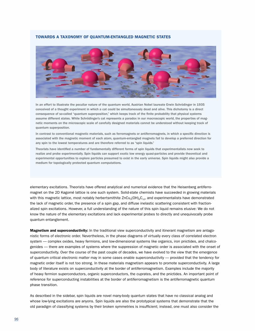
96
elementary excitations. Theorists have offered analytical and numerical evidence that the Heisenberg antiferro- magnet on the 2D Kagomé lattice is one such system. Solid-state chemists have succeeded in growing materials with this magnetic lattice, most notably herbertsmithite ZnCu3(OH)6C12, and experimentalists have demonstrated the lack of magnetic order, the presence of a spin gap, and diffuse inelastic scattering consistent with fraction- alized spin excitations. However, a full understanding of the nature of this spin liquid remains elusive: We do not know the nature of the elementary excitations and lack experimental probes to directly and unequivocally probe quantum entanglement.
Magnetism and superconductivity: In the traditional view superconductivity and itinerant magnetism are antago-nistic forms of electronic order. Nevertheless, in the phase diagrams of virtually every class of correlated electron system — complex oxides, heavy fermions, and low-dimensional systems like organics, iron pnictides, and chalco-genides — there are examples of systems where the suppression of magnetic order is associated with the onset of superconductivity. Over the course of the past couple of decades, we have evolved to the view that the emergence of quantum critical electronic matter may in some cases enable superconductivity — provided that the tendency for magnetic order itself is not too strong. In these materials magnetism appears to promote superconductivity. A large body of literature exists on superconductivity at the border of antiferromagnetism. Examples include the majority of heavy fermion superconductors, organic superconductors, the cuprates, and the pnictides. An important point of reference for superconducting instabilities at the border of antiferromagnetism is the antiferromagnetic quantum phase transition.
As described in the sidebar, spin liquids are novel many-body quantum states that have no classical analog and whose low-lying excitations are anyons. Spin liquids are also the prototypical systems that demonstrate that the old paradigm of classifying systems by their broken symmetries is insufficient; instead, one must also consider the
TOWARDS A TAXONOMY OF QUANTUM-ENTANGLED MAGNETIC STATES
In an effort to illustrate the peculiar nature of the quantum world, Austrian Nobel laureate Erwin Schrödinger in 1935 conceived of a thought experiment in which a cat could be simultaneously dead and alive. This dichotomy is a direct consequence of so-called “quantum superposition,” which keeps track of the finite probability that physical systems assume different states. While Schrödinger’s cat represents a paradox in our macroscopic world, the properties of mag- netic moments on the microscopic scale of carefully designed materials cannot be understood without keeping track of quantum superposition.
In contrast to conventional magnetic materials, such as ferromagnets or antiferromagnets, in which a specific direction is associated with the magnetic moment of each atom, quantum-entangled magnets fail to develop a preferred direction for any spin to the lowest temperatures and are therefore referred to as “spin liquids.”
Theorists have identified a number of fundamentally different forms of spin liquids that experimentalists now seek to realize and probe experimentally. Spin liquids can support exotic low energy quasi-particles and provide theoretical and experimental opportunities to explore particles presumed to exist in the early universe. Spin liquids might also provide a medium for topologically protected quantum computations.

97
structure of their entanglement. The topological nature of these low-lying states may support decoherence-resistant qubits, providing a pathway to constructing quantum computers. Studying spin liquids theoretically is still a thorny computational challenge because the frustrating magnetic interactions responsible for spin liquid behavior lead to sign problems in Monte Carlo simulations, limiting their utility. Progress has been made recently by employing tensor network methods, particularly the density matrix renormalization group (DMRG), but also the more recently intro-duced projected entangled pair state (PEPS) and tensor renormalization group (TRG) methods. DMRG methods had improved sufficiently by about five years ago to enable successful identification of spin liquid states in simple 2D frustrated magnets. However, it is still difficult to distinguish fine details of the low-lying states. For example, DMRG studies of the Kagomé Heisenberg model in 2011 [55] identified it as a gapped spin liquid, probably a “Z(2)” spin liquid, but the expected degeneracy of a factor of four for the ground state on a torus has not yet been verified (see Fig. 3.2.1).
Adding interacting conduction electrons to quantum spin liquids introduces a new range of interesting phenomena and ground states, perhaps most notable the possibility of unconventional superconductivity as discussed above. The largest body of literature exists on superconductivity at the border of antiferromagnetism. Examples include the majority of heavy fermion superconductors, organic superconductors, the cuprates, and the pnictides.
Spin-orbit coupling and magnetism in strongly-correlated systems: Advances in quantum magnetism have been intimately tied together with new materials discovery. In particular, the discovery of copper oxide-based supercon-ductors and subsequent progress in synthesizing high-quality, copper-based single crystal samples have been instrumental in advancing our understanding of quantum magnetism. Copper ions in these materials carry an S=1/2 moment, and are thus highly susceptible to quantum fluctuations. The ability to arrange such quantum spins in diverse crystal structures makes copper oxide compounds ideal candidates for studying quantum magnetism. In addition, other transition metal-based compounds, including nickelates and manganites as well as iron pnictides have played important roles in the development of current understanding of quantum magnetism. In most of these materials, orbital angular momentum is quenched due to strong crystal fields and weak spin-orbit coupling. The situ-ation is quite different for fifth-row transition metal elements, which have strong spin-orbit coupling. The magnetism in this case, for example in iridates, is described with an effective total angular momentum Jeff=1/2, arising from the interplay of the crystal field and the spin-orbit coupling. Such a small moment system is obviously an excellent candidate for studying quantum magnetism. However, what makes iridates especially exciting is that the magnetic interaction between these Jeff=1/2 moments can adopt distinct values depending on the spatial bond direction. This spin-orbit coupling effect opens up new ground compared with systems described by the well-known Heisenberg
Figure 3.2.1: Valence-bond configurations on a Kagomé lattice. (A) For each red line, the parity is set by the number of bonds crossing the line. Short loops of bonds (in red) can resonate by shifting the bonds by one site along the line, leaving the associated parity unchanged. (B), (C), A surface with genus 1 has one topologically distinct line, for which the parity can be either even or odd, leading to distinct topo-logical sectors. The two valence-bond patterns in (B) and (C) have different parities for the line in (B), but the same parity for the line in (C). Both surfaces are topologically equivalent to an open-ended cylinder.
A B C
98
interaction. On a honeycomb lattice, such bond-dependent interactions can approximate the Kitaev model, an exactly solvable model whose ground state is a quantum spin liquid. There have been intense efforts to realize the Kitaev-Heisenberg Hamiltonian in iridates. Initial interest was focused on honeycomb iridates Na2IrO3 and Li2IrO3, but recently new candidate systems such as hyper-honeycomb or harmonic- honeycomb iridates are drawing interest.
Spin-orbit torques in spintronics: Spintronics is the study of the interplay between magnetic order and transport and involves both advancing understanding of how transport properties depend on tunable magnetic states, and how electrical gate and bias voltages can be used to alter magnetic states. In the early days of its development, spintronics relied primarily on charge currents flowing through ferromagnetically ordered metals. During the last few years it has been realized that because of spin-orbit coupling, non-magnetic materials can also be a very efficient source of spin currents and spin torques, and very efficient spin-current detectors. The key enabling effects for these phenomena are spin Hall effects in which charge currents are converted into transverse spin currents and vice versa. This transverse geometry has the advantage that the ratio between spin and charge currents can be arbitrarily large, at least in principle, since each charge carrier can transfer a spin to an adjacent material multiple times, enabling therefore extremely efficient manipulation of magnetization. The transfer of spin to a magnetic nanoparticle via this mechanism does not require actual charge transport across its interface with a strongly cou-pled conductor. This property means that transverse spin transport phenomena can be used to manipulate mag-netization even in insulators in which magnetization dynamics are often extremely weakly damped. In low-damping magnetic materials with strong non-linear interactions, it has even been shown that spin-orbit torque driven mag-netization dynamics may give rise to the formation of dynamical solitons. Concomitantly, it has been realized that spin-orbit torques are very efficient at manipulating topological solitons in spin textures, such as domain walls and skyrmions (see below), and can even provide novel pathways for their generation. Similarly, spin-orbit torques have been envisioned as a possible way to control and generate magnons, and it has even been suggested that they may provide viable pathways towards generating Bose-Einstein condensates of magnons.
Skyrmions and skyrmion lattices: It has recently been discovered that bulk magnetic compounds with broken inver-sion symmetry and thin films interacting with a substrate generically form spontaneous non-trivial spin textures that are driven by chiral spin interactions. The spin textures are topological spin solitons, and can be stabilized either as isolated objects or in the form of regular lattice. In recognition of contributions by British theoretical nuclear physi-cist Tony Skyrme in the 1960s, these textures are referred to as skyrmions.
Studies of the fundamental properties of skyrmions in magnetic materials have revealed several remarkable features, in particular, greatly enhanced stability due to their non-trivial topological winding. Skyrmions provide new ways to create and destroy magnetically encoded information, efficient coupling to spin currents, which generate spin transfer torques at dramatically reduced current densities, and last but not least, a pathway to purpose-design broad-band spin dynamics devices.
Experimental and theoretical evidence that thin films, nano-wires, and nano-dots are particularly amenable to the formation of topological spin solitons such as skyrmions, underscores their exceptional potential for major break-throughs in applications. In fact, over the past year bulk materials have been discovered which support skyrmions at temperatures up to 400 K. Moreover, major advances in thin film heterostructures demonstrate that interface-asym-metry driven skyrmions at room temperature may be tailored for applications.
The most remarkable aspect connected with the discovery of skyrmion lattices are spin transfer torques many orders of magnitude more efficient as compared with conventional materials. In the context of energy relevant technology, skyrmions offer new avenues to low-dissipation data storage and data processing. This includes also implementations of high-frequency electronic devices (tailored magnonic on-chip infrastructure). Upon miniaturization of skyrmions down to the atomic levels they could become suitable for implementations of a quantum computer.
Antiferromagnetic spintronics: Magnetization texture dynamics in ferromagnetic materials driven by both electronic and magnonic spin-transfer torques have been extensively studied over the past decade, with a focus on cur-rent-driven nonlinear instabilities, and on solitonic (domain-wall/skyrmion) motion. Similar issues are now starting

99
to attract attention in antiferromagnetic metals and insulators. Key motivations include (1) the possibility of more energy-efficient and faster electrical or thermal control of solitonic motion, e.g, for memory or logic, (2) optimization of magnetization reversal dynamics in magnetic multilayers and other heterostructures, (3) classification and control of textured phases of magnetic materials (such as helical magnets and skyrmionic lattices), and (4) use of static and dynamic textures to influence electron or magnon transport (through magnetoresistive phenomena, Hall/Nerst effects, or spin pumping). Insulators, both ferro- and antiferro-magnetic, appear particularly promising for low- dissipation applications. Their thermoelectric control can in practice be enabled by spin Seebeck and spin Hall effects at interfaces with heavy metals. Collective spin transport through magnetic insulators can be realized in a regime of either easy-plane or pumped spin superfluidity, which inspires opportunities both for fundamental research and applications.
3.2.2 Scientific Challenges and Opportunities
Magnetism and superconductivity: Several key challenges are readily identified.
• A large number of systems display substantial reconstructions of Fermi surface topology across quan-tum phase transitions. This suggests that large Fermi surface fluctuations promote superconductivity. How do these properties connect with other instabilities such as charge and orbital order and strong magneto-elastic coupling?
• Superconductivity emerges in many cases from a quantum critical continuum. However, only very few examples of deviations from Fermi liquid behavior can be explained. Do we understand the nature of the normal metallic state near these phase transitions?
• Many systems are characterized by competing energy scales (the cuprates being perhaps the best example). Are there simple d-electron antiferromagnets (binary or ternary compounds) with hierarchical energy scales that display superconductivity near AFM order?
More recently several materials systems have been discovered in which superconductivity at the border of magnetism poses entirely new and unexpected challenges. These may be summarized as follows:
• Systems lacking inversion symmetry (in particular heavy-fermion materials such as CePt3Si) suggest a chiral coupling of different order parameter symmetries beyond the standard classification of uncon-ventional superconductors. There appears to be a need for a new generalized classification scheme for superconductors.
• Superconductivity in itinerant ferromagnets has so far been observed exclusively in U-based com-pounds. What makes these systems special? What is the role of orbital degrees of freedom and magneto-elastic coupling?
Spin liquids and frustrated magnetism: Progress in the study of spin-liquid states requires (1) finding and solving theoretical models exhibiting unusual many-body ground states and elementary excitations beyond one spatial dimension, (2) growing nominally defect and disorder-free materials realizing these exotic states of matter, and (3) experimentally confirming the nature of their ground states and elementary excitations. There is at present a serious gap between properties that have been identified theoretically and available experimental probes. In particular entanglement entropy seems like an attractive way to characterize states theoretically, but there is at present no obvious way of accessing it experimentally. Finding magnets with excitations in the form of non-abelian anyons could be a step toward the realization of topologically protected qubits for a quantum computer.
At the less exotic and more practical end of the spectrum there is an opportunity to make progress with materials that have artificial engineered magnetic frustration, as for example in artificial spin ice, which is a suitably designed 2D network of ferromagnetic nanowires. These nanomaterials might have applications for magnetic logic and mem-ory based on mobile domain walls, as demonstrated by Parkin’s group. The challenges which must be met if mean-ingful progress is to be achieved include (1) fabrication of large defect-free samples, (2) devising fast and reliable
100
ways of injecting, pinpointing, and moving topological defects, and (3) understanding theoretically the structure and dynamics of topological defects.
In both the spin-liquid and spin-ice examples, the challenges are in essence the same as they have been in con-densed matter physics for decades: synthesis and characterization of new materials, and achieving a theoretical understanding of observed properties. Numerical simulation of spin-liquids is essential for progress but presents several well-defined challenges. Tensor network algorithms tend to be memory intensive but difficult to parallelize. Thus the common supercomputer design with many low-memory nodes is not very useful. Systems with fewer nodes, each having larger memories (e.g., 200–1000 Gb), and job queues allowing several-month-long runs on sin-gle nodes, would be helpful.
From the theoretical point of view, some aspects of spin liquids, such as the Z(2) theory, are already well developed. A key area in which progress is possible is adapting the theory to help the computations: Given the constraints imposed by the limitations of the algorithms, can one develop diagnostics that distinguish between different ground states? What are the finite size effects associated with different spin liquid states on small systems?
Experimentally, many of the experiments discovering spin liquids have used neutron scattering, and these experi-ments are very challenging. There is a continuing need to develop new instrumentation that provides access to the lowest energy scales and the longest length scales, but with a sufficient neutron flux that weak ordered moments and inelastic scattering can be reliably probed in small single crystalline samples at low temperatures and high magnetic fields. Polarization analysis, particularly in combination with inelastic scattering measurements, is a key capability that requires further development. It is often the case that some degree of tuning will be needed to stabi-lize spin liquid states, for instance by the application of high pressures or through the application of large magnetic fields. Given the complexity of the sample environment, there is a real opportunity to combine several experimental probes with neutron scattering, such as Raman or optical spectroscopies, to accelerate the characterization of new quantum states. It is likely that, here too, more powerful neutron sources will be needed to fully exploit the range of behaviors that are anticipated. A closely related challenge is the growth of suitable large, perfect crystals. Many of the spin liquid materials have inherent complexity, for example, in having unwanted terms in their Hamiltonian, or disorder. The way around this is through the continued discovery of new materials and improved synthesis methods.
Spin-orbit coupling in strongly-correlated materials: A number of outstanding challenges are readily identified.
• Are iridates special? If not, what are other candidates for Kitaev-like model realization? The requirementfor having Jeff=1/2 moment is a d5 system in the low-spin configuration with strong spin-orbit coupling.That means Os3+ could show similar behaviour. The difficulty with safe handling of Os is a barrier forwider investigation of Os compounds. There are also some efforts to re-evaluate Ru or Rh-based mate-rials in light of recent interest in spin-orbit coupling. For example, a honeycomb magnet α-RuCl3 seemspromising for Kitaev-like magnetism despite a smaller spin-orbit interaction.
• How much of a role, if any, does the lattice degree of freedom play in determining the electronic and
magnetic properties of materials with strong spin-orbit coupling? There have been a few studies report-ing very strong lattice effects in Ba2FeReO6 and NaOsO3 but systematic studies are required, whichmay impact the application relevant area of multiferroics [293].
• Are there other interesting magnetic phases in iridates? The Weyl semimetal was first predicted forpyrochlore iridates. However, further studies have been hampered by the difficulty in growing Y2Ir2O7. Isit possible to grow single crystals of this material and to study their magnetic and electronic structure?
Spin Hall effects: So far spin Hall effects have been investigated only in a very limited range of materials. The field started with pioneering work detecting spin Hall effects in semiconductors in the early 1970s, and exploded with the discovery during the last decade that in metallic materials spin Hall effects can result in practically useful spin torques. There is nevertheless no accepted predictive understanding of torques produced by spin Hall effects. Moreover, experimental research has so far focused mostly on elemental metals and a few dilute binary alloys.
101
A wide range of materials are ripe for exploration, especially since it has been shown that sizeable spin transfer torques can also be generated from spin Hall effects in magnetically ordered materials, including antiferromagnets. In ordered materials, it has been shown that spin-orbit torques can be important even in the material that generates them, and can give rise to magnetization dynamics and switching, again even in antiferromagnets, where the torques can have the same staggered symmetry as the magnetic order.
It is understood that spin-orbit coupling phenomena in single-layer materials like transition metal dichalcogenides or topological insulator surface states can produce spin-orbit torques analogous to those produced by spin Hall effects in three dimensional systems. Except for the topological insulator case, spin-orbit torques in this class of system remain largely unexplored.
Skyrmions and skyrmion lattices: Major scientific challenges related to the fundamental properties of skyrmion lattices and individual skyrmions may be summarized as follows:
• Skyrmions and skyrmion lattices have so far been studied most extensively in the class of (cubic) B20 transition metal silicides and germanides, where they were first dicovered. Other materials classes in which skyrmions have been reported include the Perovskites and Heusler systems. Nonetheless one of the biggest challenges is the need to broaden the materials landscape to develop a much broader classification.
• Skyrmion can be stabilized in thin film structures [294]. The broad area of skyrmions in heterostruc-tures has significant application potential and merits further theoretical and experimental exploration.
• A number of theoretical studies have explored the possibility of skyrmion lattices and related topolog-ically non-trivial structures in centrosymmetric materials where they arise spontaneously because of frustrated magnetic interactions, instead of being driven by chiral interactions. An outstanding chal-lenge concerns experimental evidence for the predicted phases.
• An important scientific area that is entirely unexplored concerns the interplay of different subsystems with topological defects in their respective order parameter fields, whether magnetic, orbital, ferroic, or lattice degrees of freedom.
• Skyrmion lattices have so far been studied in systems with weak spin-orbit coupling. It would be inter-esting to study the evolution of skyrmions from weak to strong spin-orbit coupling as observed, e.g., in the iridates, thereby connecting two inherently different aspects of present day activities in magnetism.
• The skyrmions discovered so far all support the same topological winding number of -1. Are there systems supporting higher winding numbers and what are the mechanisms controlling such higher winding numbers? What are the properties of phase transitions between phases supporting different winding numbers and are there putatively quantum phase transitions between such phases?
• What are the microscopic mechanisms controlling the emergence and decay of skyrmions? Are there universal aspects of the creation and decay of skymrions and how stable are they energetically (how detrimental are quantum fluctuations to their lifetime)?
• Detailed studies have established that Berry phases in reciprocal and real space are at the heart of the intrinsic anomalous and topological Hall effect in chiral magnets. What are the consequences (manifestations) of generalized Berry phases (mixed between real and reciprocal space) in real materials?
• What are the consequences if partial order of skyrmions (e.g., liquid, nematic and smectic phases) are identified?
102
• What are the consequences of the topological spin solitons (skyrmions) in metallic systems for thenature of the metallic state and fermion quasiparticle interactions?
Antiferromagnetic spintronics: Developing and (thermoelectrically) testing heterostructures based on antiferromag-netic and other more complex magnetic insulators are needed in order to achieve regimes of efficient and long-range collective spin transport. The associated nonlinear spin texture dynamics are intriguing from the view of the energy relevant computer technologies.
3.2.3 Potential for Energy-Relevant Technologies
Magnetism and superconductivity:
• Magnetically mediated superconductive pairing is a strong contender to eventually provide room-tem-perature superconductivity, an advance that would be transformative in terms of meeting society’senergy needs.
• Superconducting spintronics based on the interplay between conventional and unconventional super-conductors and magnetism in tailored nano-systems could supplement spintronic technology.
Spin-orbit interactions in spintronics:
• The very efficient means of magnetization manipulation provided by spin-orbit torques is already beingpursued for near-future information storage and processing technologies; the non-volatility of magneticmaterials significantly reduces the need for stand-by power. Along similar lines, spin-orbit torques mayenable fatigue free memristors, which could be key to novel neuromorphic computational architec-tures. In addition, spin-orbit torques are a key ingredient to applications that harness magnetic exci-tations in insulating materials, which have truly transformational potential for low energy electronics.Using the wave-nature of long-lived magnetic excitations may furthermore enable approaches reminis-cent of quantum computation.
• Onsager reciprocals of the spin-orbit torques, in which charge currents are generated from spincurrents, are key to energy conversion at the nanoscale because they enable the transformation ofboth heat currents and mechanical orbital motion into charge voltages and currents. As such they mayenable new energy scavenging applications where excess energy is locally harvested from continuouslyrenewable energy sources, such as vibrations of thermal energy.
• The controlled generation and manipulation of magnetization dynamics at microwave and possiblyeven THz frequencies may enable novel agile oscillators and detectors. In particular, if the dynamicsof antiferromagnets can be successfully harnessed this could provide new opportunities in the THzspectrum that is not readily accessible otherwise.
• Spin-orbit torques used to generate Bose-Einstein condensed magnons or to drive spin superfluiditycould enable the room-temperature adaptation of many concepts already frequently implemented withsuperconductivity.
Skyrmions and skyrmion lattices: Challenges for applications in information technologies include:
• Determination of the precise differences and similarities between skyrmions and conventional mag-netic bubbles and the search for and identification of mixed systems (bubbles in chiral magnets).
• So far only a relatively small number of thin film and nanoscale systems have been identified thatstabilize skyrmions. What are the best (cheapest and most reliable) implementations of skyrmions inthin film and nanoscale systems (what is the best approach to tailor the underlying interactions andenergy scales)?
103
• Studies of heterostructures: Skyrmion lattices with topological insulators, skyrmion lattices with con-ventional and unconventional superconductors, skyrmion lattices with conventional magnets, and films with metallic, semiconducting and insulator skyrmion materials.
• Development of devices and applications based on topological spin solitons (skyrmions): Data storage, racetrack memory, spin torque insulators, skyrmion-based magnonics, and logic gates.
In terms of materials used for spin-orbit torques we are just at the tip of the iceberg. While the theoretical tools for describing spin-orbit coupling phenomena for bulk materials have been reasonably well established for simple materials (e.g., elemental metals), they have been rarely applied to more complex materials, and even less so for heterostructures, where the interfacial effects may dominate. At the same time, as more and more exotic materials are evaluated for their spin transport properties this will provide additional challenges for developing the processing tools that enable their incorporation into more complex heterostructures. This becomes even more problematic, if the ultimate goal is to integrate novel device concepts with existing technologies, which may have stringent processing limitations.
At the same time experimentally, the development of truly reliable metrology tools for pure spin currents is still in its infancy. The existence of current induced spin accumulations is typically only inferred indirectly. But first efforts to image spin accumulations may also bear fruit in the future for spin-orbit driven effects. This means that x-ray dichro-ism measurements may need to address a broader range of materials than just the usual 3D transition metals, and in particular may be applied more regularly at heavy element absorption edges. At the same time it will be important to image the resultant spatial distribution of magnetic excitations with spatial resolutions higher than commonly used optical inelastic spectroscopy.

104
3.3 TRANSPORT AND NON EQUILIBRIUM DYNAMICS IN QUANTUM MATERIALS
This theme crosscuts all other themes, with a focus on measurement techniques and how to understand quan-
tum materials in environments, or on time scales, never before imagined possible. The new generation of both
table-top ultra-fast lasers and accelerator-based light sources, such as LCLS, now enable access to the time
scale where electrons interact amongst themselves and are beginning to allow us to control new phases of
matter that appear during or after illumination with an intense field. From a basic science perspective, we want
to understand mechanisms underlying correlated dynamics. Ultra-fast inquiry into phase transitions, super-
conductivity, and magnetism carried out at length scales from atomic to mesoscopic are likely to lead to major
breakthroughs relevant to future energy technologies. Another important topic is transport in quantum materials,
where high field studies, optical control, inhomogeneous transport, and heterogeneous structures (multilayers)
provide fertile ground to discover and elucidate new aspects of interactions, especially when one investigates
phenomena in materials introduced in the other themesand including magnets, superconductors, topological
insulators, and multilayered devices.
3.3.1 Current Status and Recent Advances
A central goal of condensed matter physics is to try to understand and control the behavior of materials that are either driven far from their equilibrium states or are placed in extreme conditions such as high magnetic fields or electric fields and pressures. There are many reasons for this, which include (1) the ability to study materials far from equilibrium has only been enabled recently with ultra-fast pump/probe techniques; (2) the behavior of materi-als driven by strong fields is likely to lead to both new hidden phases of matter and to fast switching between states that have different behaviors (which can be employed in devices); and (3) the understanding of materials in extreme environments is a new and uncharted frontier which is likely to lead to even more interesting scientific advances. Since this field is at its infancy, techniques, theory, experiment, advanced materials synthesis, and instrumentation all need development to enable examining and exploiting this complex behavior.
At present, nonequilibrium experiments are expanding the ultra-fast frontier, operating in the few tens of femto-seconds time regime, which approaches the time scale needed to study electron dynamics [295–298]. These experiments have seen exciting new phenomena, like the appearance of transient (but in some cases long-lived) hidden phases that cannot exist under equilibrium settings, and have demonstrated the ability to rapidly manipu-late spins and spin currents with optical excitation. Figure 3.3.1 provides a conceptual overview of relevant length, time, and energy scales for quantum materials. The prospect for future ultra-fast studies is wide open and exciting. Parallel to developments in ultra-fast time-resolved measurements are developments in transport measurements. Improvements in the growth of materials and the ability to tune properties by manipulating proximity effects/inter-face/substrate effects, has ushered in the era of studying transport in 2D materials with the hopes of engineering new effects in spin versus charge transport or in valleytronic transport [299]. The ability to use large magnetic fields to suppress ordered phases and allow access to otherwise unreachable normal phases [300] is also revolutionizing the types of measurements that can be performed on complex strongly-correlated materials.

105
The time scales for many types of this strongly-correlated behavior, including switching between different phases, is orders of magnitude faster than the operating speeds of conventional electronics, suggesting that strongly-cor-related materials could be employed to revolutionize the speed of the next generation of electronic and photonic devices. The ability to control spins via electronic or optical means can greatly reduce the energy cost for switching and enhance the ability to control these systems precisely. However, more basic science research is needed to understand these systems well enough that they can be taken to the next level of development.
3.3.2 Scientific Challenges and Opportunities
Materials discovery: As the number of different atoms in the next generation of quantum materials increases, the search for new materials becomes an arduous task. It is imperative to aggressively pursue novel approaches for rap-idly exploring this vast compositional space. First introduced by the pharmaceutical industry, combinatorial method-ology is now being adopted by materials laboratories in a variety of arenas for materials discovery and optimization. Disruptive advances can be anticipated from broadening the range of local characterization techniques, including local measurements of the DC and/or microwave/THz conductivity, local structural characterization with both x-ray and ultra-fast optical spectroscopy probes from THz-mid-IR-visible, and local examination of magnetism with scanning superconducting quantum interference devices (SQUIDs). Local characterization of ultra-fast phenomena enables an efficient preview of nonequilibrium electronic, optical, and structural properties of a given material system. Close feed-back between local characterization, theory, and synthesis may allow one to obtain equilibrium versions of interesting phases through a combination of crystal growth, epitaxy, and hetero-structuring. Computational methods and theory are poised to play a major role in accelerating the process of rational discovery by “prescreening” various complex materials for the desired property or functionality. The high-throughput analysis and vast amounts of (non)-equilibrium local/imaging data pose challenges for the analysis. Yet these multidimensional parameter space results create entirely new opportunities to streamline materials discovery in combination with advanced synthesis [302, 303]. Moreover, there is a stringent demand for well-defined data management and database activities by establishing an “open source” data repository system. The quantum materials community needs to improve the rate of materials characterization to allow combinatorial pre-screening and inform the design process as the properties of the mate-rials are further refined. These procedures would benefit from a feedback loop between experiment and theory that involves a hierarchical narrowing of the parameter space as the materials properties are further improved toward the targeted design. The creation of such a class of procedures cross-cuts with the other four panels.
Figure 3.3.1: Comparison of energy, length, and time scales required to observe different physical phenomena in quantum materials. The newest frontiers tend toward the bottom corner, where they occur at short length scales, with short time delays, but over a wide range of energy scales. Pump/probe experiments that can visualize systems on the nanoscale will be optimized toward exploring these regions. We expect much new science to be ushered in as we master being able to measure phenomena through-out this schematic.
Inter-band
transitionsPersis
tent
metastable
state
Photo-excited
phase transitions,
Gap dynamics,
Lattice vib
rations
Inter-band
transitions
On-siteelectroncorrelation
CDW
Mesoscopic domain wall
Far-eldopticalresolution
Stripe or checkerboard state
energy
eV
meVÅ
nm μm
mm length
νphonon
νelectron
νlight
Ballistictransport
PlasmonsPhasepercolationDomain
randomizationTime delay
μs ns
ps fs

106
Combinatorial methods need to be pursued in parallel with other strategies requiring guiding principles. Key chal-
lenges are (i) high-quality crystalline samples in confined geometries, in which fragile forms of order can develop unimpeded by the smearing effects of disorder, (ii) tunability by pressure, electric, or magnetic fields or other param-eters, to map out complex phase diagrams and explore their potential for technological, possibly intertwined, func-tionality, (iii) measurements at the smallest length scales, the shortest time scales and under extreme conditions in order to discover, investigate, and even induce new metastable or quantum states, and (iv) the development of new theoretical concepts, with a specific focus on the optimization (smart design) of materials and devices.
Unresolved problems and new phenomena: The physics of quantum materials is rich with spectacular effects, but many of these phenomena are poorly understood. Strong (Coulomb) interactions can produce novel electronic and magnetic phases, such as high-temperature superconductivity or quantum spin liquids. The challenge is to understand how these phases evolve as a function of external perturbations such as magnetic field, pressure, and temperature. Examples include (i) an understanding of the pseudogap in high-Tc cuprates, of the charge order, and their relation to the underlying superconductivity [304, 305], (ii) an understanding of the emergence of quantum criticality in unconventional superconductors tuned by high pressures and/or high magnetic fields [141, 306], (iii) a time- and spatially-resolved spectroscopic exploration of hidden states induced in ultrathin dichalcogenide films through exposure to an intense ultra-fast laser pulse [307], and (iv) exploring entanglement through the creation and control of single electron and nuclear spins. It is recognized that despite significant technical advances our ability to probe the fundamental aspects of phase competition is still in its infancy. What is needed to achieve a basic under-standing is the ability to probe the interactions and phases over the broadest possible range of length and time scales and under the full range of relevant thermodynamic conditions of field and temperature. A major roadblock to understanding the phenomena described above is that our current suite of probes, although quite sophisticated, is inadequate to probe the full dynamic range of time and length scales of the critical fluctuations.
Additional classes of materials provide other important questions where transport and nonequilibrium phenomena play an important role. Graphene is only one example of a wide range of 2D materials, which exhibit exotic physi-cal properties when scaled to the single layer limit as compared with their bulk counterpart. Other classes of 2D materials include Dirac materials such as topological insulators and metal dichalcogenides. These material systems reveal additional emergent phenomena in the single layer limit, when compared with graphene. Entirely new phe-nomena include a prediction of topological superconductivity and Majorana zero modes in superconductor-contacted graphene [308] or the ability to control valleytronic transport optically. Another class is the chiral anomaly in Weyl semimetals, where charge can be driven between different Weyl points under parallel electric and magnetic fields [309–311]. Transport and electromagnetic signatures of these chiral effects are yet to be systematically explored in transport and spectroscopic measurements and time-resolved optical experiments. The discovery of Floquet-Bloch states in pump-probe photoemission experiments prompted several different proposals for modifying the quantum phase of a material [200]. For example, theoretical proposals show the possibility of optically inducing topological Dirac systems from trivial insulators [312], dubbed “Floquet Topological Insulators.” This phase can be realized by pumping an already gapped system with circularly polarized infrared light with energy just below the band gap. The Floquet-Bloch bands that form interact strongly with the conduction band edge and can invert, leading to topologi-cally protected helical edge states. Optoelectronic experiments can be used to search for these edge modes. Other examples include inducing an anomalous quantum Hall phase in topological insulators with axion electrodynamics [107, 313] and the realization of the long sought-after Chern insulator without Landau levels [314]. These novel systems all have some form of field-based control involved in either the creation, the stabilization, or the observation of the novel physical phenomena. We need to further develop and understand how fields control these quantum materials and how to tune them for specific behaviors.
Optical control of materials and hidden phases: Ultra-fast light experiments have already demonstrated all-op-tical magnetic switching and numerous forms of photo-induced insulator to metal transitions, with the switching being between already known equilibrium phases. An exciting new area involves the creation of so-called ‘hidden’ phases that have no equivalent in thermal equilibrium and once induced may be metastable. Observations of dynamic phase segregation during light-induced insulator-metal transitions [315, 316] indicate that the formation of nano-meter domains could be a key feature in explaining and controlling photo-induced nonequilibrium phenomena.

107
The ability to generate intense ability to generate intense far-IR and mid-IR pulses shifts the inquiry paradigm from a “passive” observation of material dynamics to “active” approaches where these pulses are used to coherently drive low-energy modes. This allows the role of a particular mode in the emergence of material functionality and its involvement in coupling across interfaces to be determined. Mode-selective ultra-fast phenomena [197] are at the frontier of modern science. One question to answer is “How do short-range interactions lead to long-range order when those interactions are still evolving with time?” In order to establish the complete experimental picture of transient magnetism, it is imperative to simultaneously probe magnetization and structure in the course of optical excitations and compare with detailed modeling. Currently developed instrumentation is beginning to allow time-resolved studies of electron-spin-lattice interactions with high element specificity, charge and spin sensitivity, nanometer resolution, and sensitivity to buried interfaces. Application of these novel techniques prom-ises revolutionary advances in both our understanding and ability to control emergent phenomena in complex quantum materials, which will be an enabling component for new energy, sensing, and information technologies.
Towards functional quantum materials: As one moves from properties of isolated materials to the properties of arrangements of different materials and heterostructures that encompass a device, a host of new issues arise which need to be examined and understood to fully realize the potential of functional quantum materials. For example, in the realm of transition metal mono-, di-, and tri-chalchogenides, opportunities exist in applications for photovoltaics, transparent electronics, enhanced lasing and plasmonic behavior, and novel electronic transistors. But to achieve any of these goals, one needs to understand how these materials interact with their substrates, with other elements/materials used for the electrical contacts, what types of proximity effects do they have, how can one tune and engineer the properties of the devices from the properties of their individual components, and how do they change in the inhomogeneous nanometer-scaled environment? This control also plays a role in engineering the dop-ing levels, the defects, and the work function mismatches at the interfaces. These studies can broadly be described as trying to understand and control the properties of the system by building the composite up from its components, but taking into account how those components modify each other synergistically. Establishing concerted efforts among experts at device material synthesis, device fabrication, transport measurement, and optical and dynam-ics studies, will be critical. On the national scale, a particular challenge is the development of facilities that allow dynamic studies of materials under extreme conditions.
Multiferroic heterostructures can be designed to allow control of magnetism with electric fields and control of ferro-electricity with magnetic fields, with potential applications in optoelectronics, spintronics, and data storage. Recent work has shown that ultra-fast optical pulses can be used to all-optically detect and control magnetoelectric coupling in these heterostructures on a time scale primarily governed by spin-lattice relaxation [317].
The generation, control, and detection of pure spin currents is a scientifically rich topic that offers a range of tech-nological opportunities. Precessing ferromagnetic magnetization emits spin currents (a phenomenon known as spin pumping [153, 154]). Conversely spin currents applied to FMs exert torques that can reduce magnetization damp-ing, to the point of driving magnetization precession and reversal [157]. These phenomena have applications to high frequency signal generation and detection and efficient writing of nanoscale magnetic memory elements, and offer the prospect of using nano magnets as amplifiers for weak magnetic signals. Recent developments suggest the pos-sibility of in operando tuning of spin currents from spin wave modes defined by the localized dipole field of scanned micromagnetic probes [158]. This offers a new horizon for controlled generation and manipulation of localized spin currents and scannable localized sources of microwave fields and spin currents. Antiferromagnets are attractive for spin-based functionality [318, 319] because they offer much higher intrinsic frequencies (THz vs GHz), and are much less sensitive to stray magnetic fields. This has motivated the study of AFs for spin current-based applications. It was recently shown that insertion of thin AF films can enhance spin currents emitted by FMs into normal metals and that AFs exhibit relatively long decay lengths [159], suggesting these could offer a promising avenue for discovery of new spin current phenomena and applications.
The discovery of highly non-equilibrium ultra-fast spin currents [320] offers another exciting prospect to investigate spin dependent scattering effects as they occur in the time domain. In order to fully exploit this effect, one must understand the interactions governing nonequilibrium spins and understand the roles of sample/interface structure.
108
The emerging spin structures need to be detected over the expected wide range of length (1–100 nm) and time scales (100 fs – 1 ns). A challenge for the theory is to model the non-equilibrium spin-torque effects beyond the conventional Landau-Lifschitz-Gilbert approximation.
Exploring coherence and entanglement with spin defects in semiconductors: In contrast to today’s technologies based on creating perfect crystals and interfaces, a nascent quantum materials platform is emerging based on defects in crystals. These defects may be created using conventional industrial ion implantation techniques through photoresist masks, resulting in patterned defects either at the surface or within the material. Quantum materials of this form may be studied by themselves, or integrated with a broad variety of systems including oxides, transi-tion metal systems, or 2D layered materials. Most recently, defects consisting of missing atoms in carbon-based semiconductors such as diamond and silicon carbide result in tightly bound individual electrons that may be easily addressed with both optical and microwave electronic techniques. These single electrons reveal extraordinarily robust quantum properties, where their spins may be optically initialized to a well-defined ground state, precisely controlled with microwaves, and read-out optically. Surprisingly, while single charge electronics has been difficult to realize, single spin electronics that operate at the quantum mechanical level is remarkable robust and persists at and above room temperature [214]. These developments reveal an exciting opportunity to engineer a new family of quantum materials by design.
Harnessing quantum mechanics at the level of single particles offers a pathway to create quantum materials with unique properties that may be controlled with magnetic, electric, or optical fields, as well as the basis for a new class of instrumentation. For example, it has been recently shown that the wavefunction of a single electron can be rapidly transferred to a single nuclear spin using optical and electronic techniques, where it serves as a single subatomic memory with long coherence times, after which it can be transferred back to the electron [321]. This process can be extended to produce a nearly 100% nuclear polarization of the material at ambient temperatures — a scenario that would normally require cooling the material to the microkelvin regime. This level of quantum control has enabled the observation of ensemble entanglement of electron and nuclear spin pairs at room temperature [216], and loophole-free Bell inequality violation using entangled electron spins separated by 1.3 kilometers [322]. Beyond information storage, high nuclear polarization is likely to have a significant impact in MRI imaging, scaling NMR to the molecular level for structure-function studies, and studies of long-distance entanglement as a means to explor teleportation with quantum materials.
It is worth noting this work also serves as the basis for a new class of quantum materials: quantum metamaterials. This emerging category defines materials that are engineered at the nanometer scale with advanced fabrication techniques to entangle normally disparate degrees of freedom — spins, photons, phonons, and microwave pho-tons — so that information is fully transformed from one state to another [218]. Recent developments have shown this to be an exciting and promising avenue for fundamental research that may lead to groundbreaking technolo-gies such as quantum repeaters. With such quantum devices, near-perfect encryption, globally-entangled quantum states, and advanced quantum computation schemes may be realized. Moreover, they will enable an advanced set of sensors operating beyond the shot noise to the quantum uncertainty limit.
Toolset
Equilibrium measurements: Linear-response measurements offer unprecedented precision that is important for understanding much of the phenomena outlined above. One example is beyond diffraction limit measurement tech-niques at microwave-THz-optical frequencies. The current resolution of scattering probes of charge/spin lies in the meV range, which is insufficient to resolve fluctuations on time scales longer than roughly 100 fs – 1 ps. Transient grating methods offer some help, but are confined to the diffraction limit, even though they can access extended time scales from picoseconds to microseconds.

109
Nonequilibrium pump/probe measurements: These techniques fall into two classes: those that attempt to mea-sure quasiparticle lifetimes near equilibrium and those that attempt to see new phases of states of matter under strongly nonequilibrium conditions. The near equilibrium optical techniques are well-developed. Time-resolved ARPES has great potential but needs to have higher resolution, sensitivity, and momentum space coverage to achieve full impact. An experimental challenge is to attain nanoscale spatial resolution in ultra-fast infrared/optical, ARPES, and x-ray experiments: breakthroughs that promise to enable investigations of nonequilibrium electronic, structural, and magnetic phenomena at the length scales commensurate with inhomogeneities in quantum materials.
3.3.3 Potential for Energy-relevant Technologies
There are many potential applications of quantum materials for energy applications that take advantage of their unique transport and non-equilibrium properties. We list some possibilities below:
• Sensing technologies for the power grid (electronic, photonic, and plasmonic)
• Predictive discovery of new functional materials (electronic, magnetic, superconducting, and phase transitions)
• Ultra-fast, energy-efficient switching and coherent transport for information processing and energy-efficient computation
• Ultra-high density magnetic storage to the atomic level
• Atomically thin and flexible devices for light detection, emission, and photovoltaics.
• Power electronics
• Ultra-low power FETs (2D materials), electronics, memory, and storage
• Plasmonics for energy harvesting and heat transfer
• Novel caloric materials based on controlled phase transitions
• Low κ interfacial materials for thermal insulation and thermoelectrics.
110
3.4 TOPOLOGICAL QUANTUM MATERIALS
Topological phases of matter are physical systems with remarkable properties. When an electronic system is in
a topological phase, physical quantities such as the Hall conductivity are expressed as either an integer multiple
of e2/h (where e is the electric charge and h is the Planck constant), or as an exact fractional multiple of e2/h.
Examples of systems with such states are 2D electron fluids in a magnetic field, and are known as the integer
and fractional quantum Hall (QH) fluids. In these states, the electric Hall current flows through the system with-
out dissipation (i.e., without energy loss).
In contrast, the value of the Hall conductivity in these electronic fluids does not change under moderate changes of sample properties (e.g., disorder) or in systems which are microscopically quite different. Such QH fluids have by now been seen in quite diverse systems such as quantum wells in AlAs-GaAs, graphene, the surface states of the 3D topological insulators, and in several other systems. This behavior is most remarkable since in ordinary electronic systems their conductivities (longitudinal and Hall) change continuously as the microscopic conditions are changed. Thus, in a generic electronic system the Hall conductivity is said to be a non-universal function of the disorder density, etc. In contrast, in integer and fractional quantum Hall states the Hall conductivity depends only on universal physical constants (e and h). The reason behind this startling behavior is due to the fact that Hall conductivity in two dimensions is given in terms of a topological invariant, known as a Chern number, a property that characterizes the wave function of the electronic system in a magnetic field. In these systems, the Hall conductivity is a topologically protected property.
A direct consequence of the topological nature of these states is that they have edge states, microscopically narrow regions at the physical edge of the sample which cannot be destroyed without destroying the topological phase and whose properties are also topologically protected. Topologically protected edge states behave effectively as chan-nels with electrical conduction without energy dissipation.
Recent theoretical and experimental research has uncovered systems that exhibit similar behaviors but without mag-netic fields: the quantum anomalous Hall effect and the quantum spin Hall effect (Fig. 3.4.1). In the more recently discovered three-dimensional topological insulators, there are edge states (at the sample surface) that behave as Dirac fermions: gapless electronic excitations that behave as relativistic particles, similarly to neutrinos (at least until the neutrino mass was discovered quite recently). These three-dimensional systems also have topologically
protected physical properties, such as a topological magneto-electric effect, which describes a surface polarization charge induced by a magnetic field.
The fractionalized topological phases have even more remarkable properties. For example, in the case of a fractional quantum Hall fluid of 2D electron fluids in magnetic fields, although the system is made of an integer number of electrons, particles that carry electric charge –e, the lowest energy excitation is a vortex of the fluid that carries fractional charge, with a value precisely determined by the topological nature of the state. Thus, removing an elec-tron from this fluid is equivalent to creating a precisely determined number of vortices in the fluid. For this reason in this state the electron is regarded as being fractionalized, split into several smaller units that can only exist inside the fluid. This fractionalization is detected in tunneling experiments that measure the fractional charge by measuring the tunneling conductance (and noise) at the edge states or in scanning capacitance experiments that measure directly the fractional charge of vortices trapped by defects in the bulk of the fluid.

111
Our three-dimensional world is made of two types of particles: fermions (electrons, protons, neutrons, neutrinos, quarks, etc.) and bosons (photons, gluons, W bosons, etc.). Atoms behave as fermions or bosons depending on whether the number of nucleons in their nucleus plus the number of electrons is odd (3He, for example, which has 2 protons, 1 neutron, and 2 electrons) or even (4He, which has one more neutron). The wave functions of a collection of identical fermions (e.g., electrons) change sign when two particles are exchanged, while bosons do not.
Vortices of fractionalized phases have fractional statistics. The wave function of a fluid with two vortices changes by a phase when the vortices are slowly exchanged during a process known as a braiding operation. If this phase is 0 the vortices are bosons, and if this phase is 𝜋 the vortices are fermions, while for values between 0 and 𝜋 they are said to be anyons. The vortices of most (but not all) fractional quantum Hall fluids have anyonic fractional statistics, which can, in principle, be measured in quantum interferometers. The conjectured fractionalized time-reversal invari-ant topological insulators have also been proposed to have vortex-like excitations with fractional statistics.
An especially important type of fractional statistics is non-abelian fractional statistics, likely to exist in the fractional quantum Hall fluid with filling fraction 5/2 (and possibly in other similar states). In these states the electrons are paired, much as in a superconductor. In the paired states, each vortex traps a special type of fermion state with zero energy known as a Majorana fermion. Majorana fermions are actually half of an ordinary fermion (without spin degeneracy) and are their own “antiparticle.” For this reason, a single Majorana fermion cannot exist in isolation but must have a partner in another vortex. Consequently, a set of four vortices has four Majorana fermions, but there are two inequivalent ways to assign them to two ordinary fermions. This means that in these systems there are
Figure 3.4.1: Imaging the quantum spin Hall Insulator using superconductivity — Fraunhofer interferometry provides a direct measure of the Fourier transform of the real space current flow pattern in a Josephson junction. Inverting the Fourier transform provides a real space image of the current flow pattern. (A) Fraunhofer pattern when the chemical potential is situated in the conduction band. (B) Real space current distribution showing a uniform current flow across the device. (C) Fraunhofer pattern when the chemical potential is situated in the topological gap. (D) Real space current distribution showing current flow through the topological helical edge states.
600
500
400
300
200
100
0
400
350
300
250
200
150
100
50
0
3500
3000
2500
2000
1500
1000
500
0
18
16
14
12
10
8
6
4
2
0
20
18
16
14
12
10
8
6
4
2
0
-4 -2 0 2 4
-4 -2 0 2 4 -8 -6 -4 -2 0 2 4 6 8
180
160
140
120
100
80
60
40
20
0-8 -6 -4 -2 0 2 4 6 8
DC c
urre
nt (
nA)
Sup
ercu
rren
t de
nsity
(nA
/μm
)
DC c
urre
nt (
nA)
Sup
ercu
rren
t de
nsity
(nA
/μm
)
Resistance (Ω)
Magnetic eld (mT)
Resistance (Ω)
Magnetic eld (mT) Position along x (μm)
Position (μm) QSHI
A
C
B
D

112
several possible allowed states, with the same energy, of four vortices with a fixed set of coordinates. Hence, when two of the vortices are braided, the wave function of the entire set of vortices becomes a linear superposi-tion of the allowed states: the state of the vortices has long-range quantum entanglement. The linear super-positions of states are encoded in a set of matrices representing the braiding operations. Under a sequence of these operations, the resulting state depends on the order of the braids, which do not commute with each other. This non-abelian property makes the vortices of these fractional quantum Hall states natural platforms for topological quantum computing, with the degenerate states playing the role of topological qubits. Other more exotic forms of fractional statistics involve particles known as parafermions and Fibonacci anyons. Majorana fermions are also expected to exist in topological super-
conductors, fractionalized states which can occur in bulk materials (possibly in Sr2RuO4) or in hybrid structures of strong spin-orbit semiconductors coupled to regular superconductors, or in hybrids of superconductors with strong topological insulators. In all of these cases, there are vortices or domain walls that trap Majorana fermion zero-modes with protected non-abelian statistics.
Three-dimensional fractionalized phases are suggested to be even more exotic. Although the possible set of 3D fractionalized phases is presently not known, some of their possible properties have been established. The
3D fractionalized phases are expected to have (closed) string-like topological defects, which can form topologically stable braids with particle-like defects. Also, at an open surface these phases should have fractionalized vortices (the end-points of the strings) with fractional (braiding) statistics.
The last decade witnessed a dramatic advancement in understanding of the role of topology in the electronic prop-erties of insulators, superconductors, and more recently, semi-metals (of the Weyl and Dirac variety). Topological insulators and semi-metals exist even in non-interacting systems, where their properties can be predicted from sym-metry considerations and simple band structure theory. In most of the known systems thus far, interactions play a minor role. However, it is anticipated that strong interactions coupled with topological effects may create completely new and unrealized states of matter.
To further advance the development of topological quantum materials and uncover novel states of matter, one needs to both pursue directions that build upon previous successful trajectories, as well as undertake new challenges, in theory, experiment, and materials synthesis. PRD-2 in Section 2.2 identifies scientific challenges to be addressed in order to move the field of topological materials forward.
3.4.1 Current Status and Recent Advances
Here we present a brief survey of some key recent accomplishments in the field that point to scientific challenges and opportunities.
Spin and anomalous Hall effects: The quantum anomalous Hall effect [326] and the quantum spin Hall effect (Fig. 3.4.1) [323] were predicted in 2006 [327–328]. The QSH effect was observed in HgTe-CdTe quantum wells
Figure 3.4.2: Theory predicted that the surface states of a strong topological insulator in three dimensions should be gapless Dirac fermions. Angle Resolved Photoemission Experiments (ARPES) and Scanning Tunneling Microscopy experiments on the surface of the strong topological insulator Bi2Se3 confirmed this theoretical prediction. The ARPES spectrum of these surface states, shown in this figure, has the characteristic features of Dirac fermions: a conduction band and a valence touching at the Dirac point. Further spin-polarized ARPES experiments confirmed another prediction: that the spin of the fermions is locked to the momentum of the fermion [325].

113
shortly afterwards [329]. The QAH effect, although predicted even earlier (in 1988) in a simple (but unrealistic) model [330], was observed experimentally only much more recently in a thin film of the magnetic topological insulator (Bi,Sb)2Te3 [331, 332].
Dirac fermion surface states: A key feature of the 3D strong TI phase is that it has protected gapless Dirac fermi-ons on exposed surfaces [325, 333–335]. Dirac fermions were found experimentally by STM experiments in BixSb1-x [234] and by ARPES experiments in Bi2Se3 (Fig. 3.4.2) [325], which detected the spin-momentum locking of Dirac fermions. Shubnikov-de Haas magnetic oscillation experiments in high magnetic fields further established the Dirac nature of the surface states by detecting the relativistic Landau levels [336].
Chiral anomaly and Fermi arcs in Weyl semimetals: Weyl semimetals are topological states of matter with remark-able properties. These semimetals may arise in pyrochlore iridate materials, such as Y2Ir2O7 [14], and have been found experimentally in materials such as TaAs [12]. The electronic states in the bulk have two bands that cross at two points of the Brillouin zone separated by a lattice momentum k0. Close to these crossings the electronic bands resemble two Weyl fermions. It is known [337] that the charge current of each Weyl fermion is not separately conserved, a phenomenon known as the chiral anomaly. However, the two Weyl fermions carry opposite chirality and their anomalies cancel each other out, and only the total charge current is conserved. In the presence of parallel electric and magnetic fields, a polarization current is induced between the two Weyl fermions and an associated neg-ative magneto-resistance. These are manifestations of the chiral anomaly [338–340]. These effects have recently been observed experimentally in the Weyl semimetal TaAs (Fig. 3.4.2) [12], which can lead to potential applications of the chiral anomaly in devices. A startling feature of Weyl semimetals is that they have a metallic surface state with the peculiar property that its Fermi surface is reduced to a Fermi arc (spanned by the momentum k0) with the seemingly missing part of the Fermi surface on the opposite surface of the crystal. Fermi arcs have recently been seen in ARPES experiments [341].
Interacting topological materials: Once correlations are added, a new class of topological systems becomes possi-ble: this currently includes the rare earth based compounds SmB6, Nd2T2O7, and RBiPt with magnetic rare earths, or topological superconductors (TSCs). A theoretical prediction that the Kondo insulator is a Z(2) topological state [39, 342] was confirmed in experiments in the heavy fermion material SmB6 [343, 344]. This discovery opened a new area of research in the field of topological systems, the strongly-correlated topological insulators.
On the TSC side, a material of great interest is the p-wave superconductor Sr2RuO4 (SRO) [345]. It was proposed [346] that SRO has a px+ipy superconducting order parameter. This is a topological superconducting state, which
Figure 3.4.3: In Weyl semimetals the electronic conduction and valence bands touch at pairs of points of the Brillouin zone of momen-tum space. A prediction from theory is that on opposite surfaces the electronic surface states of Weyl semimetals have Fermi arcs. This prediction is surprising, since Fermi surfaces must form closed contours in momentum space. However, in Weyl semimetals the arcs are connected (and close) to each other through the bulk of the material (as shown in the figure). Fermi arcs have been discovered recently in ARPES experiments in the topological material TaAs.
Co-propagating Fermi Arcs
ν
ν
+ –
L
y
yx
kxkz
B
B
+ –
-0.2
-0.4
-0.6
-0.2 0.0 0.2
kx (Å-1)
kx
k ν
k x (
Å-1)
E E+∆E

114
has been predicted to have a Majorana zero-mode in the core of a half vortex [62]. On the experimental side, phase-sensitive measurements showed that Sr2RuO4 is indeed an odd-parity (p-wave) superconductor [347]. Kerr effect experiments [348] showed that the superconducting state breaks time reversal invariance. Chiral domains were detected in magnetic field modulation of critical currents in Josephson junctions [349]. An experiment on a mesoscopic sample of Sr2RuO4 with annular geometry provided evidence for the predicted half vortices in this superconductor [350]. However, scanning Hall bar and quantum interference experiments [351] did not detect the expected spontaneous currents in the superconducting state of Sr2RuO4, a result that has raised questions on the identification of the pairing state.
3.4.2 Potential for Energy-Relevant Technologies
Two of the main technological challenges we are currently facing are to reduce the amount of dissipation generated in electronic devices and to discover new modes of computation that are inherently more efficient than the existing ones. Topological insulators and topological superconductors hold promise in both areas. The topological nature of edge modes and the transport associated with them may hold promise in future applications where dissipation-less transfer of information across a device is needed. Furthermore, localized Majorana modes have the desired prop-erties needed for implementing topological quantum computation. Quantum computing, in general, provides a new computation paradigm that can make solving certain problems far more efficient (and hence consume less energy). A topological approach to quantum computing is particularly appealing in the context of energy dissipation, since quantum operations are generated as adiabatic manipulation of the ground state of the system and hence maintain the system in equilibrium.
One likely impact of work on topological materials is the development of new kinds of electronic devices based on topological states. Phenomena such as protected edge states and fractional quasiparticles have many potential uses, and it remains to be seen where their greatest uses will lie. In the following section we outline some areas where new electronic functionalities are enabled by topological materials. In some cases (e.g., low-dissipation inter-connects based on edge states) the path forward is relatively clear, while in other cases considerable work remains to be done in understanding how to connect these remarkable scientific discoveries to technology.
Energy and information are the essential parts of our modern society. Much energy transport occurs over the power grid, delivering electricity to every corner of modern life. However, a significant fraction of the energy is lost due to dissipation inside wires. Rapid progress of our information society is based on Moore’s law, which states that the number of transistors on a semiconductor chip doubles every 18 months. However, the problem of heat dissipation in wires now makes it impossible to pack more transistors on a semiconductor chip and still run them at full speed. When the charged electron moves inside metals and semiconductors, it is constantly scattered by impurities and other electrons, so that its energy is rapidly dissipated. A grand challenge in basic energy science is to discover mechanisms and organizational principles for dissipationless transport in solids. Such discovery could dramatically save energy delivered over the power grid, and enable continued shrinking of semiconductor circuits.
There are two known mechanisms of dissipationless transport of electrons in solids. In the superconducting state, electrons form Cooper pairs and condense into a macroscopic quantum state characterized by a complex order parameter and vanishing electrical resistance. Topological insulators in magnetic and non-magnetic materials offer another possible mechanism of dissipationless transport, where the electron spin degree of freedom plays a crucial role. In a time reversal invariant 2D topological insulator, the bulk interior is insulating, and electrical conduction occurs only on the edge, where opposite spin states counter-propagate due to spin-orbit coupling. In this quantum spin Hall state, when electrons on the edge encounter a non-magnetic impurity, two possible backscattering paths related by time reversal symmetry interfere with each other destructively, forbidding elastic backscattering. Inelastic backscattering is still possible with loss of electron phase coherence. When time reversal symmetry is broken by magnetic order in a topological insulator, the degeneracy between the two counter-propagating edge states is removed. In this case, one of the edge states can be destroyed while the other survives as a chiral edge state, giving rise to the so-called quantum anomalous Hall effect. In this novel electronic state, electrons at a given edge

115
can only move in one direction, preventing both elastic and inelastic backscattering and thus rendering electri-cal conduction dissipationless. Recently, the quantum anomalous Hall effect has been theoretically predicted and experimentally observed in Cr doped Bi2Te3 topo-logical insulators, where the precise quantization of the Hall plateau and the vanishing four point resistance has been experimentally measured.
Superconductivity is difficult to predict: To date, almost all superconductors are discovered experimentally, largely by trial and error. In contrast, theoretical under-standing of topological materials is far more advanced, and most topological insulators are predicted before their experimental observation. The exponential increase of computing power enables efficient search and design of topological materials. At this point, the quantum anomalous Hall effect is observed at low temperature. However, the two crucial ingredients of the quantum anomalous Hall effect, the topological band structure and magnetic order, could in principle exist at room tem-perature. Stanene is a new class of 2D material, where tin atoms form a 2D honeycomb lattice similar to the structure of graphene. Due to the large spin-orbit coupling of the heavy element tin, the topological gap is predicted to be 300meV, far greater than the energy scale of room temperature. Many ferromagnetic materials are known to have a Curie temperature far greater than room temperature. Therefore, quantum anomalous Hall effect provides a new direction towards dissipationless transport at room temperature, addressing one of the greatest grand chal-lenge problems in basic energy science. Theoretical design and prediction could guide the search for the desired topological material in a highly efficient manner.
In the area of infrared photonics, topological insulators show great promise in the context of low frequency photon detectors and energy conversion. Moreover, the feature of an intrinsic topologically protected metal on top of an insulator can be exploited for fast and reliable “self-assembly” if progress can continue to be made on the materials side. It was pointed out in ref. [352] that in a thin film geometry, the overlap of wavefunctions of top and bottom surface states can open small micro-gap structures in the density of states with an energy δ (see Fig. 2.2.2). Such surface band gaps can be used to make sensitive photodetectors or be used in IR photovoltaics. In principle such technology may be a competitor for conventional (Hg1-xCdx)Te (MCT) detectors in the mid-infrared range. Although it arises in a different fashion, the surface band gap would be like that MCT technology in that in the simplest case, its band gap would be set by materials and geometric configurations and although tunable would be fixed for a particular detector. With regards to photovoltaics it has been proposed that the pristine surfaces of Bi2Se3 have an intrinsic band bending that could generate up to ~75 meV of surface photovoltage on illumination [353]. This means that TIs could operate as intrinsic metal-insulator Schottky barrier solar cells with an estimated maximum efficiency of ∼7% according to the Shockley-Queisser criterion. Similarly, if the bulk of TI can be differentially doped to form p- and n-type regions, TIs would form novel self-assembled photocells with the surface states playing the role thattransparent conducting indium tin oxide plays in conventional photocells. Coupled with their self-assembly features,TIs are an excellent candidate in a number of different forms for low cost solar cells.
The properties of topological materials also make them promising hosts for plasmonic circuits. Plasmons are coupled excitations of electrons and electromagnetic fields in solids. They localize electromagnetic energy at the nanoscale, which makes them vital for next generation high density optically assisted magnetic data storage tech-nology [297] and for enhancement of light-harvesting photovoltaic applications [354]. Their manipulation and control is an area of great current interest. Despite the tremendous success of modern plasmonics, it has been recognized
Figure 3.4.4: Resulting surface band structure with divergences in joint density of states for 1-photon (α1) and 2-photon (δ) transitions.
116
that the typically used noble metals have limitations, particularly in the blue-UV part of the spectrum, which has led to the search for alternative plasmonic materials. It has been pointed out that in general, Dirac systems have plasmons with relatively long propagation lengths compared with their wavelengths and, from the possibility to gate them, tunable energies [355]. For instance, it has recently been shown [356] that in topological insulator Bi1.5Sb0.5Te1.8Se1.2 (BSTS) single crystals, a combination of surface optical conductivity from topologically protected surface states and bulk optical conductivity related to the dispersion created by the interband transitions in the medium gives a new mechanism for visible and UV plasmonic response. It is expected that with improvements, the functional frequency range of topological materials as plasmonic materials will be expanded and their tenability exploited. Moreover, it is expected that TIs in thin film form can be readily incorporated into plasmonic circuits for energy harvesting applications.
In conclusion, the area of topological materials is incredibly promising and there are reasons to think that we have only just scratched the surface of what is known and experimentally possible. Already for non-interacting systems we have discovered phases that have been shown to be theoretically possible [60, 61, 357] such as two and three dimensional topological insulators; quantum spin Hall and quantum anomalous Hall states; Chiral surface states in Weyl semimetals; promising first signatures of exotic excitations known as Majorana zero modes; and many more. Moreover, the interplay of interactions and topology is expected to be incredibly rich with a large number of new topologically distinct phases possible. When one considers the possibility of interfacing topological materials to other states of matter, the possibilities for novel states of matter and new and unexplored phenomena become virtu-ally limitless. Many of the observed and predicted phenomena and phases discussed in this PRD were not known a decade ago. It is, therefore, very likely that our projections of what is interesting and promising captures only a small fraction of what will be discovered.
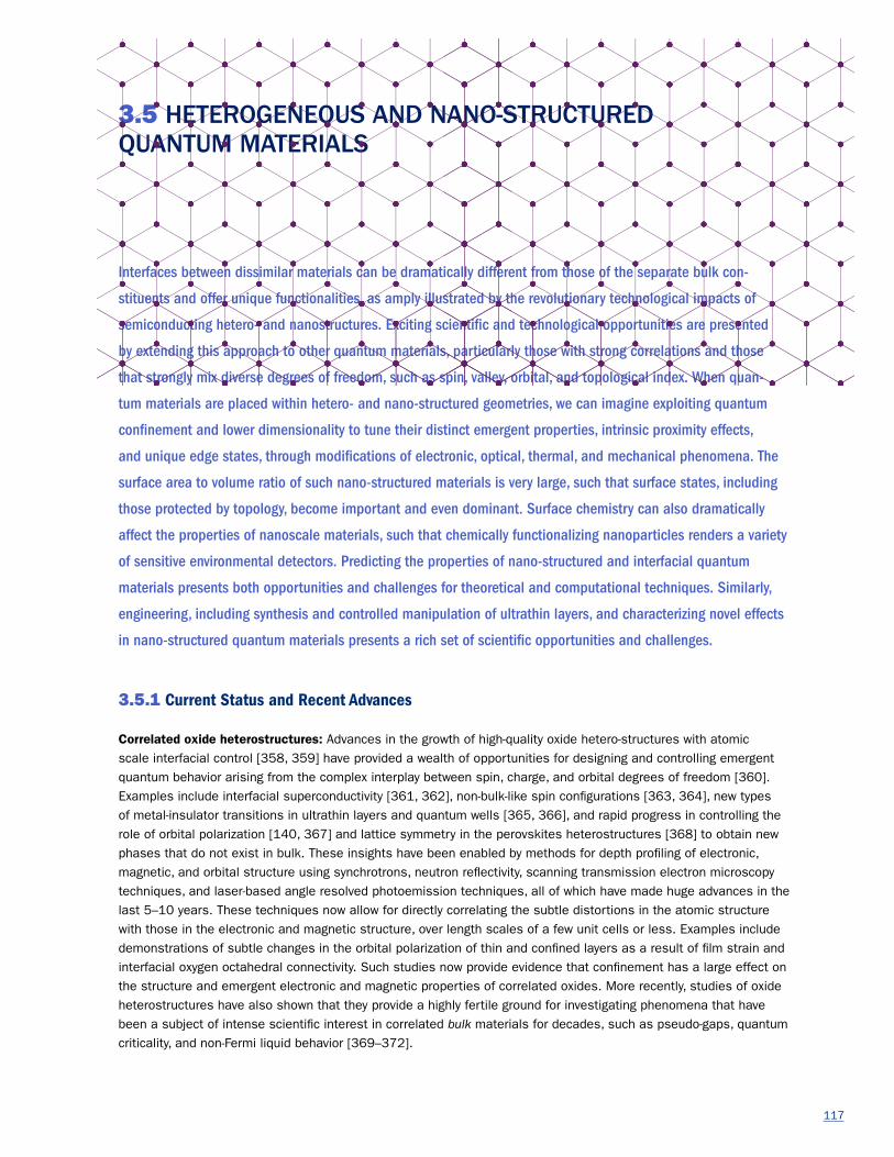
117
3.5 HETEROGENEOUS AND NANO-STRUCTURED QUANTUM MATERIALS
Interfaces between dissimilar materials can be dramatically different from those of the separate bulk con-
stituents and offer unique functionalities, as amply illustrated by the revolutionary technological impacts of
semiconducting hetero- and nanostructures. Exciting scientific and technological opportunities are presented
by extending this approach to other quantum materials, particularly those with strong correlations and those
that strongly mix diverse degrees of freedom, such as spin, valley, orbital, and topological index. When quan-
tum materials are placed within hetero- and nano-structured geometries, we can imagine exploiting quantum
confinement and lower dimensionality to tune their distinct emergent properties, intrinsic proximity effects,
and unique edge states, through modifications of electronic, optical, thermal, and mechanical phenomena. The
surface area to volume ratio of such nano-structured materials is very large, such that surface states, including
those protected by topology, become important and even dominant. Surface chemistry can also dramatically
affect the properties of nanoscale materials, such that chemically functionalizing nanoparticles renders a variety
of sensitive environmental detectors. Predicting the properties of nano-structured and interfacial quantum
materials presents both opportunities and challenges for theoretical and computational techniques. Similarly,
engineering, including synthesis and controlled manipulation of ultrathin layers, and characterizing novel effects
in nano-structured quantum materials presents a rich set of scientific opportunities and challenges.
3.5.1 Current Status and Recent Advances
Correlated oxide heterostructures: Advances in the growth of high-quality oxide hetero-structures with atomic scale interfacial control [358, 359] have provided a wealth of opportunities for designing and controlling emergent quantum behavior arising from the complex interplay between spin, charge, and orbital degrees of freedom [360]. Examples include interfacial superconductivity [361, 362], non-bulk-like spin configurations [363, 364], new types of metal-insulator transitions in ultrathin layers and quantum wells [365, 366], and rapid progress in controlling the role of orbital polarization [140, 367] and lattice symmetry in the perovskites heterostructures [368] to obtain new phases that do not exist in bulk. These insights have been enabled by methods for depth profiling of electronic, magnetic, and orbital structure using synchrotrons, neutron reflectivity, scanning transmission electron microscopy techniques, and laser-based angle resolved photoemission techniques, all of which have made huge advances in the last 5–10 years. These techniques now allow for directly correlating the subtle distortions in the atomic structure with those in the electronic and magnetic structure, over length scales of a few unit cells or less. Examples include demonstrations of subtle changes in the orbital polarization of thin and confined layers as a result of film strain and interfacial oxygen octahedral connectivity. Such studies now provide evidence that confinement has a large effect on the structure and emergent electronic and magnetic properties of correlated oxides. More recently, studies of oxide heterostructures have also shown that they provide a highly fertile ground for investigating phenomena that have been a subject of intense scientific interest in correlated bulk materials for decades, such as pseudo-gaps, quantum criticality, and non-Fermi liquid behavior [369–372].
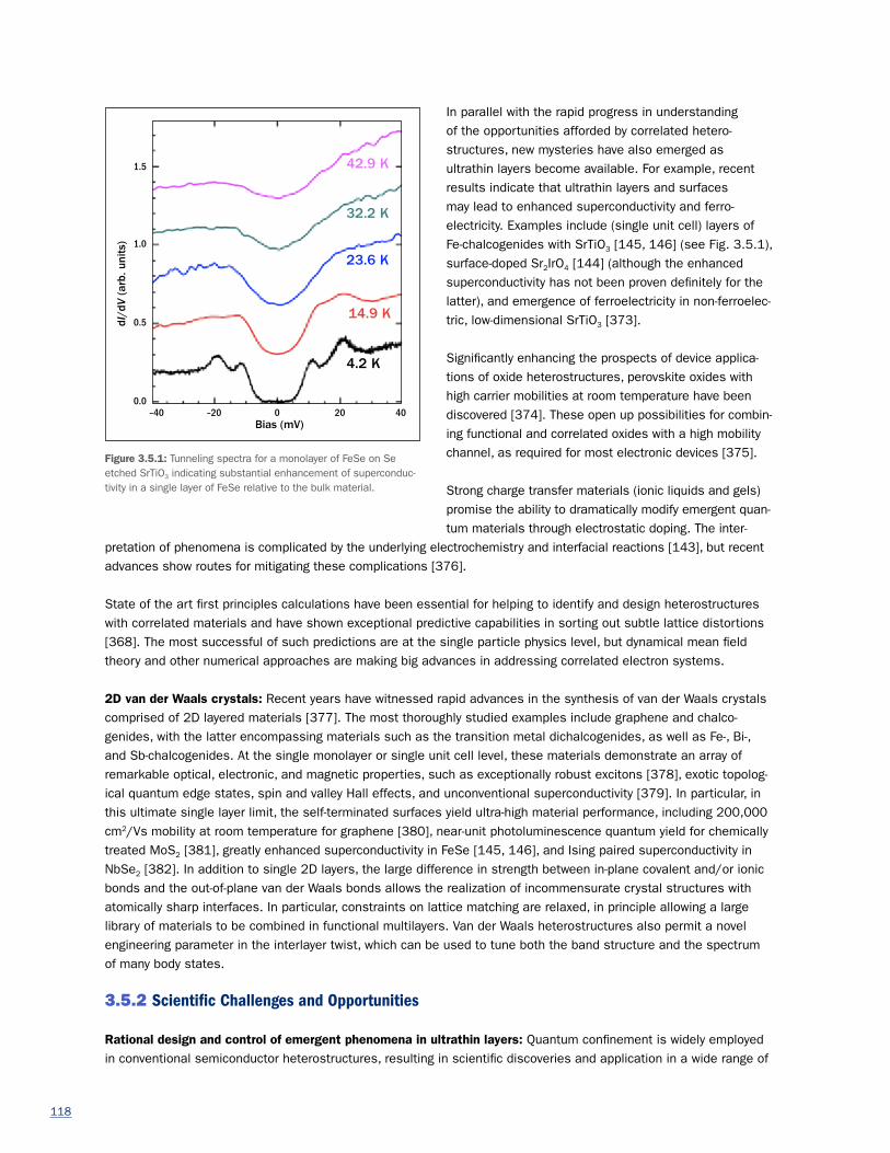
118
In parallel with the rapid progress in understanding of the opportunities afforded by correlated hetero-structures, new mysteries have also emerged as ultrathin layers become available. For example, recent results indicate that ultrathin layers and surfaces may lead to enhanced superconductivity and ferro-electricity. Examples include (single unit cell) layers of Fe-chalcogenides with SrTiO3 [145, 146] (see Fig. 3.5.1), surface-doped Sr2IrO4 [144] (although the enhanced superconductivity has not been proven definitely for the latter), and emergence of ferroelectricity in non-ferroelec-tric, low-dimensional SrTiO3 [373].
Significantly enhancing the prospects of device applica-tions of oxide heterostructures, perovskite oxides with high carrier mobilities at room temperature have been discovered [374]. These open up possibilities for combin-ing functional and correlated oxides with a high mobility channel, as required for most electronic devices [375].
Strong charge transfer materials (ionic liquids and gels) promise the ability to dramatically modify emergent quan-tum materials through electrostatic doping. The inter-
pretation of phenomena is complicated by the underlying electrochemistry and interfacial reactions [143], but recent advances show routes for mitigating these complications [376].
State of the art first principles calculations have been essential for helping to identify and design heterostructures with correlated materials and have shown exceptional predictive capabilities in sorting out subtle lattice distortions [368]. The most successful of such predictions are at the single particle physics level, but dynamical mean field theory and other numerical approaches are making big advances in addressing correlated electron systems.
2D van der Waals crystals: Recent years have witnessed rapid advances in the synthesis of van der Waals crystals comprised of 2D layered materials [377]. The most thoroughly studied examples include graphene and chalco-genides, with the latter encompassing materials such as the transition metal dichalcogenides, as well as Fe-, Bi-, and Sb-chalcogenides. At the single monolayer or single unit cell level, these materials demonstrate an array of remarkable optical, electronic, and magnetic properties, such as exceptionally robust excitons [378], exotic topolog-ical quantum edge states, spin and valley Hall effects, and unconventional superconductivity [379]. In particular, in this ultimate single layer limit, the self-terminated surfaces yield ultra-high material performance, including 200,000 cm2/Vs mobility at room temperature for graphene [380], near-unit photoluminescence quantum yield for chemically treated MoS2 [381], greatly enhanced superconductivity in FeSe [145, 146], and Ising paired superconductivity in NbSe2 [382]. In addition to single 2D layers, the large difference in strength between in-plane covalent and/or ionic bonds and the out-of-plane van der Waals bonds allows the realization of incommensurate crystal structures with atomically sharp interfaces. In particular, constraints on lattice matching are relaxed, in principle allowing a large library of materials to be combined in functional multilayers. Van der Waals heterostructures also permit a novel engineering parameter in the interlayer twist, which can be used to tune both the band structure and the spectrum of many body states.
3.5.2 Scientific Challenges and Opportunities
Rational design and control of emergent phenomena in ultrathin layers: Quantum confinement is widely employed in conventional semiconductor heterostructures, resulting in scientific discoveries and application in a wide range of
Figure 3.5.1: Tunneling spectra for a monolayer of FeSe on Se etched SrTiO3 indicating substantial enhancement of superconduc-tivity in a single layer of FeSe relative to the bulk material.
–40 –20 0 20 40
dI/d
V (a
rb. u
nits
)
Bias (mV)
1.5
1.0
0.5
0.0
42.9 K
32.2 K
23.6 K
14.9 K
4.2 K

119
device technologies. Even richer physics is expected in heterostructures with correlated materials. For exam-ple, electron-electron interactions in transition metal oxides give rise to emergent phenomena, such as unconventional superconductivity and unique magnetic states. Confinement strongly alters these interactions. Heterostructures provide opportunities to answer some of the most pertinent questions in correlated materials systems, such as separating the roles of electronic and lattice degrees of freedom in metal-insulator transitions or the origins of high-temperature superconductivity. They allow for orbital, structural, and bandwidth control to design correlated states and exotic phenomena from the ground up (Figure 3.5.2). They could also be used to tune layers close to quantum phase transitions to allow for electric field or strain control of correlated phenom-ena. These opportunities have barely been exploited.
Developing solid-state control of electronic, magnetic, orbital, and optical properties would provide a powerful platform for understanding the mysteries of correlated electron systems and also enable programmable and adaptive materials. The full bag of “epitaxy tricks” (complex superlattices, patterned substrates, unconven-tional crystallographic orientations, Stranski-Krastonow growth, strain, etc.) has not yet been fully exploited for new quantum materials, but would offer access to new phenomena, such as new topologies or frustrated magnetism. Interfaces between oxides with differing cation-anion polyhedra types may yield new approaches to electronic and orbital reconstructions, in which disparate crystal field effects are exploited to alter the local band structure. Finally, the growth orientation can be used to control the interfacial polarity, the number of competing interfacial exchange interactions, and topology of confined layers. Currently such efforts are limited by the availability of substrates, but greater collaboration between single crystal growth and epitaxial film growth would enable new opportunities in this area. Increasing the complexity of heterostructures, for example superlattices consisting of three or more constituent materials, would enable new approaches for studying the competing interactions in correlated oxides.
Designing emergence in hybrid 2D van der Waals crystals: As mentioned above, the van der Waals interaction in principle enables the relatively unconstrained assembly of complex heterogeneous 2D materials whose individual constituents could be metals, semimetals, semiconductors, superconductors, ferromagnets, antiferromagnets, or insulators. This presents numerous opportunities for engineering quantum phenomena of both fundamental and technological importance. The most immediate extension of existing concepts from semiconductor quantum struc-tures arises from the observation that the van der Waals bonding may enable unpinned band alignment at semicon-ductor interfaces. Thus, in contrast with traditional semiconductor heterostructures wherein the band alignment is predetermined by material-dependent band offsets, the band alignment in van der Waals quantum heterostructures may be tunable via external fields, allowing in operando tunable wavelength light emission. At a more fundamental level, proximity between diverse monolayer constituents may allow the engineering of new atomically thin meta-materials whose properties depend on the interplay between different order parameters such as magnetism and superconductivity. Such an interplay is likely to yield emergent phenomena, particularly when mixed in with reduced dimensionality, strong quantum confinement, and enhanced Coulomb interactions.
Figure 3.5.2: Structure tuning knobs in heteroepitaxial perovskite films. Shown are the octahedra formed by the oxygens that surround the transition metal ions and frequently show different tilt and rotation patterns. In heterostructures, they are controlled via interfacial coupling and strain, and determine functional properties such as magnetism, metal-insulator transitions, and orbital polarization.
epitaxiallm
cubicsubstrate
epitaxial strain
interfacial coupling
inte
ract
ion
dist
ance
octahedralcontrol parameter
heterointerface
z
xy

120
The opportunities provided by the assembly of 2D materials into complex arrangements are, however, accompa-nied by serious challenges that span the entire scientific gamut, ranging from difficulties in materials synthesis to difficulties in our theoretical understanding. For instance, as mentioned in the chapter on crystal growth, wafer-scale synthesis of single-domain monolayers and heterostructures remains an unsolved problem, despite recent progress in the wafer scale growth of homogeneous but polycrystalline TMD monolayers by metal organic chemical vapor deposition [222]. The proof-of-concept demonstrations of mechanical stacking of 2D materials into multilayers is not a viable route toward practical devices operating at the performance limit. We need to explore new strategies for controlled synthesis of single-domain monolayers and multilayer heterostructures with tuned composition. We also need to carry out detailed characterization and spatial mapping of defects and to understand their effect on the electronic band structure and majority/minority carriers. It will be important to develop routes to fixing/repairing defects to enable “perfect” materials to explore fundamental 2D material performance at the ideal limit. In addition, means of creating deterministic defects could enable a pathway to further control quantum phenomena and local band structure within these materials. Another challenge to be addressed is the further reduction of dimensional-ity of 2D materials by nanopatterning into one dimensional (1D) and zero dimensional (0D) devices: Even though we now have excellent control over synthesis of 2D mono- and di-chalcogenide thin films, they remain challenging to synthesize (or pattern) into pristine nanostructures whose properties are intrinsic. Thus, we need to develop strategies for nanopatterning of these materials into devices of similar quality as has been achieved in conventional semiconductors. Finally, as we mentioned earlier, recent experimental work has shown how control over the twist angle in 2D multilayers can modify electronic structure [383]. However, accurate modeling of the electronic structure in twisted multilayers challenges the ability of ab initio theory to quantitatively predict electronic properties.
CONTROLLED, HIGH-PURITY SAMPLES OF QUANTUM MATERIALS
Detailed investigation of the intrinsic physical prop-erties of materials and the use of these properties in applications often requires high-purity samples. This is especially true in the realm of quantum materials. Even at very low defect densities, structural and composi-tional disorders and their associated strain effects can profoundly affect the ground state of strongly-correlated systems. Such disorders can also mask the signatures of electronic phase transitions. In the ultra-clean limit, recent observations suggest that hydrodynamic effects might also be relevant for electronic transport and could lead to entirely new physical regimes for exploration. Furthermore, subtle electronic states exist close to the boundary of competing phases. Precise control of the stoichiometry is a prerequisite both for determining the intrinsic properties of a stoichiometric “parent,” and for controlling the balance between competing phases. Producing high-purity samples of quantum materials necessitates the development of synthesis methods in which defect type, density, and distribution are system-atically defined and controlled. In some cases, quantum materials of interest are already the subject of extensive
research in the broader fields of solid-state chemistry and materials science, and avenues for crystal growth, thin film deposi-tion, etc. may already have been developed and studied for their own intellectual merit. However, for the majority of cases the synthesis of quantum materials has not been studied with such rigor. Consequently, considerable effort is necessary in order to determine suitable synthesis conditions. A wide spectrum of techniques can be brought to bear on this effort, the choice depending on a variety of material-specific and application-specific factors.
Photograph of single crystals of the high-temperature supercon-ductor YBa2Cu3O7-δ grown at the University of British Columbia. Development of appropriate crucible technology, and control of crystalline perfection, oxygen vacancy concentration, oxygen vacancy ordering, and twin boundary density, were all critical in order to enable key measurements that probe the intrinsic electronic properties of this material.

121
3.6 CROSS-CUTTING THEMES
In parallel with progress in fundamental science is progress in the corresponding scientific methods. To vary-
ing degrees, scientists are engaged in and motivated by both pursuits. In this section we discuss the essential
crosscutting themes of synthesis, instrumentation, and theory and modeling. Rather than reiterating the scien-
tific motivations, this section focusses on the enabling methodologies and technologies that drive progress in all
of the main themes.
3.6.1 Materials Synthesis
Materials synthesis is crucial for all experimental studies of quantum materials, motivating intense research into the optimal methods to grow/deposit/prepare materials of current interest. Furthermore, the discovery of new quantum materials, or methods to artificially structure them, has been the continuous source of new, unex-pected discoveries that define the next frontiers of the field. Thus, the synthesis of new materials with specific ground states and/or functionality, or the discovery of new phenomena in materials tuned in specific ways, is of central importance and requires extensive scien-tific research that is as fundamental and challenging in nature as the challenges described in the preceding sections. Research in materials synthesis also con-nects directly to all attempts at predictive “materials by design” as the necessary validating step in any predic-tive process. Reflecting the central role of materials synthesis, this cross-cutting theme explores the impor-tance, challenges, and opportunities for the “science of synthesis” as it relates to the field of quantum materials.
Current status and recent advances
A wide range of synthesis tools and techniques are currently employed to create and tune quantum materials in a variety of physical forms, including bulk polycrystalline, single crystal and amorphous materials, metastable phases, reduced dimensional crystals (2D sheets and nanocrystals), thin films, and heterogeneous materials. Ground states and excitations of these materials are often sensitive to disorder, and a major effort is needed to identify and control relevant defects in order to prepare high-purity samples (see the sidebar “Controlled, high purity samples of quantum materials”). Similarly, such materials are also often character-ized by near-degenerate electronic phases which can be influenced by suitable chemical substitution, and it is often necessary to determine methods to tune the materials in desired ways. In order to admit specific measurement techniques, or to enable specific functionality, materials are also often patterned or processed in a variety of ways; for the purpose of this cross-cutting theme, we regard these processing steps as part of the synthesis process broadly construed.
Figure 3.6.1: Advances in furnace technology open new avenues for the synthesis of quantum materials. One such recent advance is the development of the laser diode heated floating zone furnace (shown above); the large temperature-gradients that can be achieved in such furnaces not only help control nucleation, but also provide access to metastable phases. The lower panel shows a photograph of a single crystal of BiFeO3 as an example of materials that can be grown by this technique.
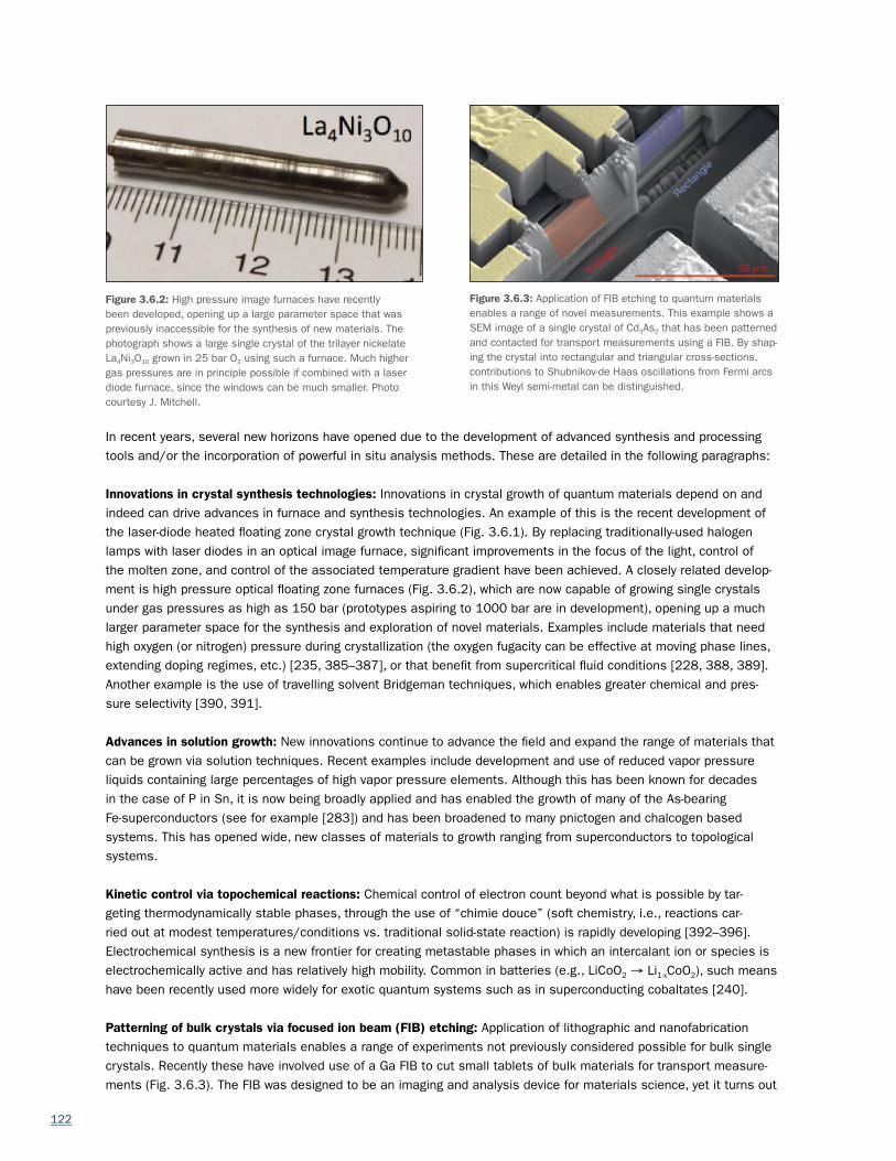
122
In recent years, several new horizons have opened due to the development of advanced synthesis and processing tools and/or the incorporation of powerful in situ analysis methods. These are detailed in the following paragraphs:
Innovations in crystal synthesis technologies: Innovations in crystal growth of quantum materials depend on and indeed can drive advances in furnace and synthesis technologies. An example of this is the recent development of the laser-diode heated floating zone crystal growth technique (Fig. 3.6.1). By replacing traditionally-used halogen lamps with laser diodes in an optical image furnace, significant improvements in the focus of the light, control of the molten zone, and control of the associated temperature gradient have been achieved. A closely related develop-ment is high pressure optical floating zone furnaces (Fig. 3.6.2), which are now capable of growing single crystals under gas pressures as high as 150 bar (prototypes aspiring to 1000 bar are in development), opening up a much larger parameter space for the synthesis and exploration of novel materials. Examples include materials that need high oxygen (or nitrogen) pressure during crystallization (the oxygen fugacity can be effective at moving phase lines, extending doping regimes, etc.) [235, 385–387], or that benefit from supercritical fluid conditions [228, 388, 389]. Another example is the use of travelling solvent Bridgeman techniques, which enables greater chemical and pres-sure selectivity [390, 391].
Advances in solution growth: New innovations continue to advance the field and expand the range of materials that can be grown via solution techniques. Recent examples include development and use of reduced vapor pressure liquids containing large percentages of high vapor pressure elements. Although this has been known for decades in the case of P in Sn, it is now being broadly applied and has enabled the growth of many of the As-bearing Fe-superconductors (see for example [283]) and has been broadened to many pnictogen and chalcogen based systems. This has opened wide, new classes of materials to growth ranging from superconductors to topological systems.
Kinetic control via topochemical reactions: Chemical control of electron count beyond what is possible by tar-geting thermodynamically stable phases, through the use of “chimie douce” (soft chemistry, i.e., reactions car-ried out at modest temperatures/conditions vs. traditional solid-state reaction) is rapidly developing [392–396]. Electrochemical synthesis is a new frontier for creating metastable phases in which an intercalant ion or species is electrochemically active and has relatively high mobility. Common in batteries (e.g., LiCoO2 → Li1-xCoO2), such means have been recently used more widely for exotic quantum systems such as in superconducting cobaltates [240].
Patterning of bulk crystals via focused ion beam (FIB) etching: Application of lithographic and nanofabrication techniques to quantum materials enables a range of experiments not previously considered possible for bulk single crystals. Recently these have involved use of a Ga FIB to cut small tablets of bulk materials for transport measure-ments (Fig. 3.6.3). The FIB was designed to be an imaging and analysis device for materials science, yet it turns out
Figure 3.6.2: High pressure image furnaces have recently been developed, opening up a large parameter space that was previously inaccessible for the synthesis of new materials. The photograph shows a large single crystal of the trilayer nickelate La4Ni3O10 grown in 25 bar O2 using such a furnace. Much higher gas pressures are in principle possible if combined with a laser diode furnace, since the windows can be much smaller. Photo courtesy J. Mitchell.
Figure 3.6.3: Application of FIB etching to quantum materials enables a range of novel measurements. This example shows a SEM image of a single crystal of Cd3As2 that has been patterned and contacted for transport measurements using a FIB. By shap-ing the crystal into rectangular and triangular cross-sections, contributions to Shubnikov-de Haas oscillations from Fermi arcs in this Weyl semi-metal can be distinguished.
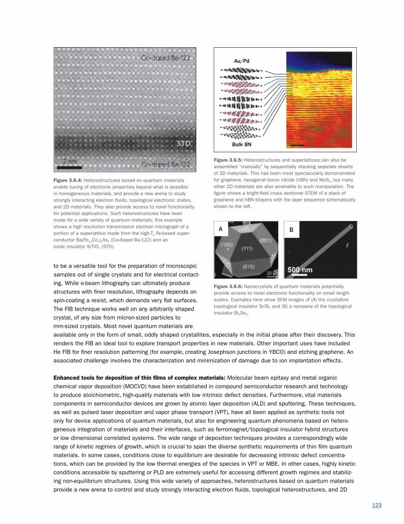
123
to be a versatile tool for the preparation of microscopic samples out of single crystals and for electrical contact-ing. While e-beam lithography can ultimately produce structures with finer resolution, lithography depends on spin-coating a resist, which demands very flat surfaces. The FIB technique works well on any arbitrarily shaped crystal, of any size from micron-sized particles to mm-sized crystals. Most novel quantum materials areavailable only in the form of small, oddly shaped crystallites, especially in the initial phase after their discovery. Thisrenders the FIB an ideal tool to explore transport properties in new materials. Other important uses have includedHe FIB for finer resolution patterning (for example, creating Josephson junctions in YBCO) and etching graphene. Anassociated challenge involves the characterization and minimization of damage due to ion implantation effects.
Enhanced tools for deposition of thin films of complex materials: Molecular beam epitaxy and metal organic chemical vapor deposition (MOCVD) have been established in compound semiconductor research and technology to produce stoichiometric, high-quality materials with low intrinsic defect densities. Furthermore, vital materials components in semiconductor devices are grown by atomic layer deposition (ALD) and sputtering. These techniques, as well as pulsed laser deposition and vapor phase transport (VPT), have all been applied as synthetic tools not only for device applications of quantum materials, but also for engineering quantum phenomena based on hetero-geneous integration of materials and their interfaces, such as ferromagnet/topological insulator hybrid structures or low dimensional correlated systems. The wide range of deposition techniques provides a correspondingly wide range of kinetic regimes of growth, which is crucial to span the diverse synthetic requirements of thin film quantum materials. In some cases, conditions close to equilibrium are desirable for decreasing intrinsic defect concentra-tions, which can be provided by the low thermal energies of the species in VPT or MBE. In other cases, highly kinetic conditions accessible by sputtering or PLD are extremely useful for accessing different growth regimes and stabiliz-ing non-equilibrium structures. Using this wide variety of approaches, heterostructures based on quantum materials provide a new arena to control and study strongly interacting electron fluids, topological heterostructures, and 2D
Figure 3.6.6: Nanocrystals of quantum materials potentially provide access to novel electronic functionality on small length scales. Examples here show SEM images of (A) the crystalline topological insulator SnTe, and (B) a nanowire of the topological insulator Bi2Se3.
Figure 3.6.4: Heterostructures based on quantum materials enable tuning of electronic properties beyond what is possible in homogeneous materials, and provide a new arena to study strongly interacting electron fluids, topological electronic states, and 2D materials. They also provide access to novel functionality for potential applications. Such heterostructures have been made for a wide variety of quantum materials; this example shows a high resolution transmission electron micrograph of a portion of a superlattice made from the high-Tc Fe-based super-conductor Ba(Fe1-xCox)2As2 (Co-doped Ba-122) and an oxide insulator SrTiO3 (STO).
Au/Pd
Bulk BN
Figure 3.6.5: Heterostructures and superlattices can also be assembled “manually” by sequentially stacking separate sheets of 2D materials. This has been most spectacularly demonstrated for graphene, hexagonal boron nitride (hBN) and MoS2, but many other 2D materials are also amenable to such manipulation. The figure shows a bright-field cross sectional STEM of a stack of graphene and hBN bilayers with the layer sequence schematically shown to the left.

124
materials (Fig. 3.6.4). Analagous to III-V semiconductors heterostructures, where each major step in materials perfection has brought on new science, we expect the same to be the case for other quantum materials.
Integration of advanced in situ surface analysis tools with thin film deposition: Materials such as Bi2Se3 and monolayer FeSe on SrTiO3 have driven and benefitted from the development of a range of in situ surface analysis tools, including STM and ARPES, which enable detailed characterization of the electronic properties of ultrathin film samples and which also promise rapid feedback for improvements in synthesis conditions.
Integration of synchrotron-based tools in thin-film and bulk synthesis: Building on considerable investment from federal funding agencies, tools including in situ real-time x-ray scattering and diffraction from thin film, powder, and even liquid phase samples have been developed, providing time-resolved information relevant to understanding growth mechanisms and synthesis pathways.
Development of techniques to engineer heterostruc-tures from 2D layered materials: Entirely new classes of “engineered” quantum materials have become possible (Fig. 3.6.5) based on manipulation and stacking of
sheets of exfoliated 2D layered materials, such as graphene, BN and MoS2, opening the doorway to a new level of control of emergent electronic properties [377].
Single crystal nanomaterials: Recent advances in the synthesis and characterization of single crystal nanomaterials (Fig. 3.6.6) have revealed electronic properties comparable to bulk counterparts [403]. These include topological insulator nanoribbons and plates, which show Aharonov-Bohm oscillations and for which the Fermi level can be tuned to study the surface states [404, 405]; van der Waals materials such as a single- or double-layer graphene, hBN, MoS2, and other transition metal dichalcogenide nanosheets [377, 406]; and semiconducting nanowires such as InSb nanowires used as a platform to study Majorana fermions [122]. For single crystal nanomaterials, a variety of synthetic approaches can be employed, such as vapor-liquid-solid growth, chemical vapor deposition, metal organic chemical vapor phase deposition, atomic layer deposition, etc.
Exploratory materials discovery: The advent of the new tools and techniques outlined above does not obviate the continuing need for and use of well-established synthesis techniques (such as time-honored solid-state synthesis techniques, and crystal growth via Bridgman, Czochralski, and flux methods) all of which remain highly relevant and effective for the synthesis of many quantum materials [408]. Many materials classes of current interest were first synthesized in polycrystalline form, and this trend will likely remain valid in the future. For example, the rich field of superconductivity in Fe-based compounds was initiated by pioneering work on polycrystalline LaFePO and LaFeAsO1-xFx [241, 409], while the detailed physical properties of this broad family of compounds has been estab-lished via a wide spectrum of experiments performed on high-quality bulk single crystals, which were mainly syn-thesized via established methods (Fig. 3.6.7). In other words, the process of materials discovery and development draws on a foundation of well-established and continually refined methods, the sustained practice of which is as important for the ongoing vitality of research in the broad field of quantum materials as is the development of new synthesis techniques and methodologies.
Figure 3.6.7: Rapid availability of single crystals of a variety of Fe-based superconductors has enabled swift progress in estab-lishing the fundamental physics of these materials. Innovation in fluxes, as well as methods to contain and handle toxic materials with high vapor pressures, were necessary in order to safely pro-duce high-quality samples. Even so, these materials are typically grown by standard solution techniques, emphasizing the fact that new materials are often synthesized via traditional methods. Use of solution based techniques also leads to discoveries of new compounds, such as CaFe2As2, which had not previously been grown in polycrystalline form. The photograph shows a single crystal of (Ba1-xKx)Fe2As2 over a mm scale.
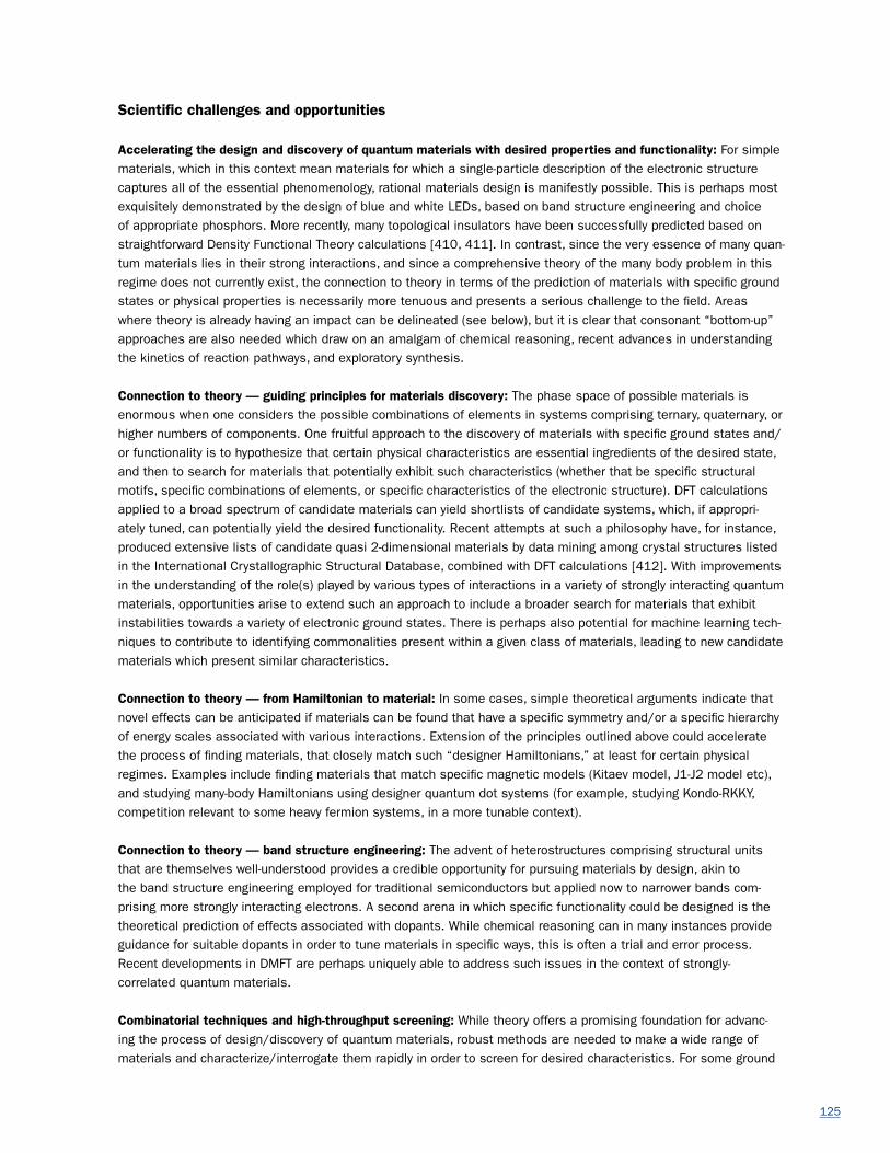
125
Scientific challenges and opportunities
Accelerating the design and discovery of quantum materials with desired properties and functionality: For simple materials, which in this context mean materials for which a single-particle description of the electronic structure captures all of the essential phenomenology, rational materials design is manifestly possible. This is perhaps most exquisitely demonstrated by the design of blue and white LEDs, based on band structure engineering and choice of appropriate phosphors. More recently, many topological insulators have been successfully predicted based on straightforward Density Functional Theory calculations [410, 411]. In contrast, since the very essence of many quan-tum materials lies in their strong interactions, and since a comprehensive theory of the many body problem in this regime does not currently exist, the connection to theory in terms of the prediction of materials with specific ground states or physical properties is necessarily more tenuous and presents a serious challenge to the field. Areas where theory is already having an impact can be delineated (see below), but it is clear that consonant “bottom-up” approaches are also needed which draw on an amalgam of chemical reasoning, recent advances in understanding the kinetics of reaction pathways, and exploratory synthesis.
Connection to theory — guiding principles for materials discovery: The phase space of possible materials is enormous when one considers the possible combinations of elements in systems comprising ternary, quaternary, or higher numbers of components. One fruitful approach to the discovery of materials with specific ground states and/or functionality is to hypothesize that certain physical characteristics are essential ingredients of the desired state, and then to search for materials that potentially exhibit such characteristics (whether that be specific structural motifs, specific combinations of elements, or specific characteristics of the electronic structure). DFT calculations applied to a broad spectrum of candidate materials can yield shortlists of candidate systems, which, if appropri-ately tuned, can potentially yield the desired functionality. Recent attempts at such a philosophy have, for instance, produced extensive lists of candidate quasi 2-dimensional materials by data mining among crystal structures listed in the International Crystallographic Structural Database, combined with DFT calculations [412]. With improvements in the understanding of the role(s) played by various types of interactions in a variety of strongly interacting quantum materials, opportunities arise to extend such an approach to include a broader search for materials that exhibit instabilities towards a variety of electronic ground states. There is perhaps also potential for machine learning tech-niques to contribute to identifying commonalities present within a given class of materials, leading to new candidate materials which present similar characteristics.
Connection to theory — from Hamiltonian to material: In some cases, simple theoretical arguments indicate that novel effects can be anticipated if materials can be found that have a specific symmetry and/or a specific hierarchy of energy scales associated with various interactions. Extension of the principles outlined above could accelerate the process of finding materials, that closely match such “designer Hamiltonians,” at least for certain physical regimes. Examples include finding materials that match specific magnetic models (Kitaev model, J1-J2 model etc), and studying many-body Hamiltonians using designer quantum dot systems (for example, studying Kondo-RKKY, competition relevant to some heavy fermion systems, in a more tunable context).
Connection to theory — band structure engineering: The advent of heterostructures comprising structural units that are themselves well-understood provides a credible opportunity for pursuing materials by design, akin to the band structure engineering employed for traditional semiconductors but applied now to narrower bands com-prising more strongly interacting electrons. A second arena in which specific functionality could be designed is the theoretical prediction of effects associated with dopants. While chemical reasoning can in many instances provide guidance for suitable dopants in order to tune materials in specific ways, this is often a trial and error process. Recent developments in DMFT are perhaps uniquely able to address such issues in the context of strongly- correlated quantum materials.
Combinatorial techniques and high-throughput screening: While theory offers a promising foundation for advanc-ing the process of design/discovery of quantum materials, robust methods are needed to make a wide range of materials and characterize/interrogate them rapidly in order to screen for desired characteristics. For some ground

126
states of current interest (for example, unconventional superconductors), a combinatorial approach would likely fail due to the sensitivity of the ground state to disorder. However, opportunities exist in the context of materials properties that are more robust to disorder (for example, thermoelectric power), and for obtaining approximate phase diagrams associated with varying dopants in given systems. An important issue is pairing the synthe-sis with an equally high-throughput measuring technique that gives appropriate feedback.
Bottom-up synthesis strategies: Established synthesis strategies are continually being refined, but the drive for new, controlled materials calls for innovative methodolo-gies, such as those inspired by recent findings that inor-ganic materials can be built from preexisting, structurally defined units present in fluxes or solutions. To coin a word, these units may be called inorganic “synthons” (inspired from Corey’s definition used in organic synthe-sis or in the field of metal-organic framework chemistry, in which “synthons” refers to the pre-defined organic
molecules that connect with other pre-defined molecules of metal centers). Can we develop inorganic synthon strat-egies that can control discrete atomic scale monomers to create new quantum materials (Fig. 3.6.8)? A long-term goal would be to understand and control synthons that can be associated with calculable, quantitative descriptors of their character — electronegativity, magnetism, coordination number, size, and structure — that can lead to classification of reactivity. The grand hope is that this process would ultimately lead to classifying reaction types for synthons and to the predictive design, discovery, and growth of new materials, surpassing trial-and-error approaches that lack generality from one system to the next. Experimental efforts in this emerging direction are promising but are still very much in their infancy.
Exploratory synthesis: Large databases exist describing the structure and composition of a wide range of known materials (for example, Pearson’s Handbook of Crystallographic Data for Intermetallic Phases, or the web-based Inorganic Crystal Structure Database). Such databases provide starting points for experimental synthesis efforts aimed at finding bulk materials with specific characteristics, and for theoretical efforts for which detailed knowledge of the stable crystal structure is a vital first step. The properties of many phases found in these tables are not known in detail, and there exists an opportunity for applying computational and data-mining techniques to identify candidate materials with specific functionality (as described above). However, it is important to realize that these tables are not complete. The phase space of possible materials is enormous, and the need for an experimentally driven exploratory synthesis program is as great now as it has ever been. There are many approaches that can be taken, including studying previously unexplored/under-explored elements or combinations of elements, deliberately targeting certain structures or structural motifs, developing novel fluxes and solutions, etc. Such studies are often undertaken with a specific set of ideas in mind, and the exploratory process is as much a way to test/validate/falsify those ideas as it is a way to discover new materials. Similarly, the sustained exploration of the wide phase space of possible materials populates useful databases with new materials, which in turn provides insight and guidance for the targeted search for materials with desired properties.
Improvement and innovation in synthesis, processing techniques, and sample quality
With every new material there are necessarily challenges associated with optimizing synthesis and processing con-ditions in order to achieve the desired level of purity or other relevant figure(s) of merit (see the sidebar “Controlled, high purity samples of quantum materials”). For bulk crystals, an additional issue is often achieving samples with an appropriate volume to enable specific measurements. While co-mounting several smaller crystals is a possibility, this can degrade the quality of the data by adding extraneous material and broadening the mosaic. For example, for
Figure 3.6.8: There are many open questions about the nature and role of preformed structural units present in the melt for inorganic materials, illustrated schematically here. Can such “synthons” be controlled to provide targeted pathways to realize new quantum materials?

127
many materials of current interest single crys-talline samples are currently only available with sub-mm dimensions: Larger samples would allow mapping of the low energy spin excitations via inelastic neutron scattering. Similar requirements for large high-quality single crystals are also essen-tial for THz spectroscopy. The approach to solving this ongoing challenge takes different forms for different materials. In all cases, though, a common feature is the dedication of time and resources by practitioners skilled in the science of synthesis.
“Panoramic” synthesis: Although theory can sometimes suggest or predict new materials with desired or exotic properties, it does not offer a means or a method to obtain these materials, which is left as a challenge to the synthetic chem-ist and/or crystal grower. Another challenge that cannot be currently addressed with a theoretical strategy is what will happen when two or more reagents react under certain conditions. What materials will form? A completely new framework for predicting synthetic pathways of inorganic materials (including quantum materials), and their crystallization pathways, is needed and would transform how materials by design is approached. What is missing is the means to systematically explore in situ, in real time and with feedback, the creation of materials from solid state to melt and back to provide a “panoramic view” of the synthesis space (Fig. 3.6.9). New approaches need to be developed that will lead to phase control by understanding materials building rules and the subsequent classification of reaction types that offer synthetic predictability and, hopefully generality and portability within related systems.
High pressure synthesis: The spectrum of possible materials is not limited solely to phases that are thermodynam-ically stable at 1 atmosphere, but includes also metastable phases quenched from high pressure. High pressure synthesis, which is not currently widely represented in the U.S., provides access to a wide array of possible (meta-)stable phases that are not otherwise accessible, broadening the “palette” of available materials. High pressure syn-thesis also provides means to grow some thermodynamically stable materials by either shifting the composition-tem-perature phase diagram to access desired phases (for example, MgB2) or by suppressing vapor pressures of volatile elements (for example RFeAsO/F). At present, the field of high pressure synthesis in the U.S. is sparsely populated, with isolated “one-offs” rather than sustained lines of success. Opportunities for advances do not necessarily involve inventing new techniques or regimes of high pressure growth, but rather harnessing existing state of the art ones to open new avenues of investigation for quantum materials.
Enhanced deposition methods: Significant challenges still exist in many of the deposition techniques applied to quantum materials systems, in particular, stoichiometry control and the wide range of volatility of many constituents for these complex materials. In many cases, these issues are closely related. In PLD and sputtering, volatile com-ponents can lead to off-stoichiometric deposition, which has been empirically compensated by target composition, or off-axis geometries. However, a deeper understanding of these non-equilibrium deposition processes is essential for fundamental progress, including the transient ‘molecular’ state of the deposition species. For MBE, MOCVD, and ALD, an important priority is continued investment in developing new and innovative deposition approaches, such as, advanced elemental and compound evaporation sources, and new metal-organic sources; significant time investment is required for each new materials system. To take advantage of the ultrahigh purity growth environment, which yields superior materials, cross-contamination must be avoided. This essentially limits each growth system to a single materials family.
Figure 3.6.9: Traditional synthesis methods are “blind”: products are formed from reagents, but little is known about intermediate compounds. Here, in situ x-ray diffraction is used to reveal a sequence of phase transformations in the K-Cu-S system. By stopping the reaction at the appropriate moment, kinetically trapped materials can be produced. There is a huge opportunity associated with obtaining such a “panoramic” view of a reaction, both in terms of devising synthesis strategies that target certain types of compounds, and in terms of discovering new materials that are not thermodynamically stable.
0 30 60 90
Scal
e (a
rb. u
nits
)
50°C 50°C
K2S3
K3Cu4S4
K3Cu8S6
K2S3
KCu3S2Cu
600°C
Time (min)

128
Opportunities also exist for advanced combinatorial approaches for atomically engineered materials that would allow for the automated use of multiple deposition capabilities using advanced robotic techniques. For complex hetero-structures of quantum materials, this allows for the use of the optimal growth technique for each constituent, and is particularly important when in situ transfer is required to atomically control and preserve surfaces and interfaces. An important consideration is such a large-scale integration of growth techniques requires a similar integration of expertise and facilities on a scale beyond typical single-PI efforts.
In-depth characterization of surface/interface processes: In situ techniques have proven powerful to investigate the intrinsic properties of quantum materials, avoiding undesirable and complicated surface parasitic effects that occur when samples are left in air. However, for potential applications, a critical component of fundamental research is investigating ways to process materials such that their surface properties are either controlled or well character-ized. So far, efforts in this direction have not been emphasized.
Other processing approaches — E-beam and optical lithography for novel materials: How do these processing steps, often performed in widely shared clean room facilities, need to be modified to work with a wide variety of materials (including, for instance, lower processing temperatures, concerns about alkali developers, e-beam/ion damage, etc.)? What form factors of samples are consistent with lithography? Techniques need to be developed to apply resist in place of spinning it on, including, for example, direct write or projection optical lithography in place of common contact mask aligners. In terms of shadow masks, what resolution can be achieved? Can they be used for etching or just physical vapor deposition? What are cross-contamination issues in processing, especially dry etching (e.g., ion mill, reactive ion etch, and plasma)? Facilities need to grapple with these issues if these tech-niques are to be more widely applied to quantum materials. Furthermore, mesoscale devices based on integrated heterostructures of quantum materials often require the close coordination of multiple synthesis and processing steps. Examples include the use of underlying hard masks and etching layers, and subsequent growth on patterned structures. We also note that a critical difference between low-dimensional and bulk materials is extreme sensitivity to surface contamination. Thus the residues left by conventional polymer resists, which are a minor issue for bulk materials, are a central concern for atomically thin sheets. However, traditional methods of surface cleaning, such as plasma treatment, can severely damage atomic layers. New lithography and patterning techniques that do not contaminate surfaces will provide a fundamental advance.
Development of improved substrates for 2D materials: For 2D materials, the substrate can be as important as the material itself. In particular, we note the need for synthesis of large-area hexagonal boron nitride or an equivalent insulator that provides a match for 2D conductors/semiconductors. There is a lot of work in this area but it is still a weak link. hBN has revolutionized the study of graphene and beyond — but only on the scale of exfoliated flakes.
3.6.2 Instrumentation
Quantum materials are often characterized by competing nearly-degenerate states, where phase competition and the coexistence of multiple phases lead to structural and electronic inhomogeneities on a wide range of length scales, from atomic to mesoscopic dimensions (see Fig. 3.6.10). The attractiveness of these materials — with their unusually rich phase diagrams that support useful crystallographic, electronic, magnetic, and superconducting phases with frustrations and degenerate ground states — is at the same time the origin of the immense experimen-tal challenge for understanding and exploiting them. Thus many quantum materials, whether recently discovered or under scrutiny for decades, still defy understanding and cannot be fully exploited for technology.
Continued advances in developing “new windows into quantum materials” is absolutely central for scientific prog-ress and critical for realizing the technological potential of quantum materials. While there has been tremendous progress in the capabilities of instrumentation over the past decade, with ensuing discoveries and understand-ing, there are many exciting new opportunities. As we discuss below, since 2010 there have been revolutionary advances in light sources spanning the x-ray to the THz region of the spectrum, with exquisite control over the
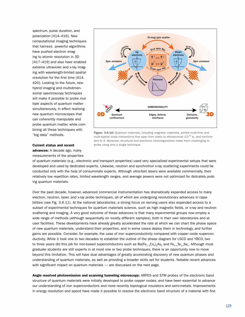
129
spectrum, pulse duration, and polarization [414–416]. New computational imaging techniques that harness powerful algorithms have pushed electron imag-ing to atomic resolution in 3D [417–419] and also have enabled extreme ultraviolet and x-ray imag-ing with wavelength-limited spatial resolution for the first time [414, 420]. Looking to the future, new hybrid imaging and multidimen-sional spectroscopy techniques will make it possible to probe mul-tiple aspects of quantum matter simultaneously, in effect realizing new quantum microscopes that can coherently manipulate and probe quantum matter, while com-bining all these techniques with “big data” methods.
Current status and recent advances: A decade ago, many measurements of the properties of quantum materials (e.g., electronic and transport properties) used very specialized experimental setups that were developed and used by dedicated experts. Likewise, neutron and synchrotron x-ray scattering experiments could be conducted only with the help of consummate experts. Although ultra-fast lasers were available commercially, their relatively low repetition rates, limited wavelength ranges, and average powers were not optimized for delicately prob-ing quantum materials.
Over the past decade, however, advanced commercial instrumentation has dramatically expanded access to many electron, neutron, laser, and x-ray probe techniques, all of which are undergoing revolutionary advances in capa-bilities (see Fig. 3.6.11). At the national laboratories, a strong focus on serving users also expanded access to a subset of experimental techniques for quantum materials science, such as high magnetic fields, or x-ray and neutron scattering and imaging. A very good outcome of these advances is that many experimental groups now employ a wide range of methods (although sequentially on mostly different samples), both in their own laboratories and at user facilities. These developments have already greatly accelerated the rate at which we can chart the phase space of new quantum materials, understand their properties, and in some cases deploy them in technology, and further gains are possible. Consider, for example, the case of iron superconductivity compared with copper oxide supercon-ductivity. While it took one to two decades to establish the outline of the phase diagram for LSCO and YBCO, two to three years did this job for iron-based superconductors such as Ba(Fe1- xCox)2As2 and Fe1+yTe1-xSex. Although most graduate students are still experts in at most one or two probe techniques, there is an opportunity now to move beyond this limitation. This will have dual advantages of greatly accelerating discovery of new quantum phases and understanding of quantum materials, as well as providing a broader skills set for students. Notable recent advances with significant impact on quantum materials — are discussed on the next page.
Angle resolved photoemission and scanning tunneling microscopy: ARPES and STM probes of the electronic band structure of quantum materials were initially developed to probe copper oxides, and have been essential to advance our understanding of iron superconductors and more recently topological insulators and semi-metals. Improvements in energy resolution and speed have made it possible to resolve the electronic band structure of a material with fine
Figure. 3.6.10: Quantum materials, including magnetic materials, exhibit multi-time and multi-spatial scale interactions that span from static to attoseconds (10-18 s), and centime-ters to Å. Moreover, structural and electronic inhomogeneities make them challenging to probe using only a single technique.
El-mag spin scatter
DIMENSIONALITY
Quantumconnement
Edges, defects,interfaces
Domains,granularity
Phonons
Lase
r puls
e Laser pulse
Spin emissionSpin emission
Upelectrons
Downelectrons
El-el collision
El-e
l col
lision
El-ph spin ip
El-el spin ip
El-ph
colli
sion
El-ph collision
T
μ
T
μ
0D 3D

130
detail. When combined with ultra-fast lasers, deep-ultraviolet (deep-UV) ARPES is making it possible to achieve meV energy resolution with medium time resolution (see Fig 3.6.12). Laser-driven extreme UV high harmonic sources are making it possible to access the full Brillouin zone of a material, with ultra-fast time resolution (≈ few femtoseconds)[421]. As a result, it is now possible to visualize the ensemble-averaged spin-resolved band structure of a quantum material with either high energy resolution (i.e., meV energy resolution to see the fine details in the band structure that encode the material symmetry and order) or with high ≈10 fs time resolution (i.e., ≈0.1eV energy resolution, to probe, for example, how fast the material can change its state). By visualizing the electronic structure of a material in real time after excitation by light, the multiple nanoscale mechanisms responsible for ultra-fast metal-to-insulator phase transitions or ultra-fast magnetic state switching can be visualized. New light-induced Floquet-Bloch states in topological insulators — which are hybrid photon-electron states that appear only while an excitation laser beam is present — have also been observed [200]. Finally, driven amongst other things by the excitement of probing and understanding quantum materials, experimental work at high magnetic fields has also advanced tremendously in the past decade to provide essential information about band structure, phase transitions, and collective phenomena in topological materials, quantum magnets, and superconductors.
Imaging science using photons and electrons: Microscopic imaging is critical to advances in materials and energy sciences, as well as to nanoelectronics, data storage, and medicine. The heterogeneity inherently present in many quantum materials makes imaging a critical tool for understanding their many phases and harnessing their remark-able properties. Fortunately, there is a revolution underway in all areas of photon- and electron-based microscopy, fueled by new coherent light sources, advanced detectors, improved electron optics, as well as computational imag-ing techniques [423].
It is now possible (albeit still only in a few laboratories worldwide) to use electron microscopy to probe materials with ~0.5Å resolution [424]. As discussed in the sidebar “Coherent X-ray Imaging: A Lensless Microscope,” x-ray imaging is undergoing a revolution due to the availability of coherent, laser-like x-ray beams, that, when combined
Figure 3.6.11: Current tools for probing quantum materials have advanced considerably. In the future, more powerful and hybrid probes will be needed to probe structural and electronic inhomogeneities on mult-time and multi-spatial scales.
1.0
0.5
0.0
-0.5
-1.0
E–E F (e
V)kll (Å-1)
0.0 0.2 0.4 0.6 0.8 1.0
200 fs
1 2
3
y (μm)0 100
x (nm)
1
0
∆t (
ps)
Nano-probes X-ray imaging Electron imaging
Extreme elds Neutron probes ARPES
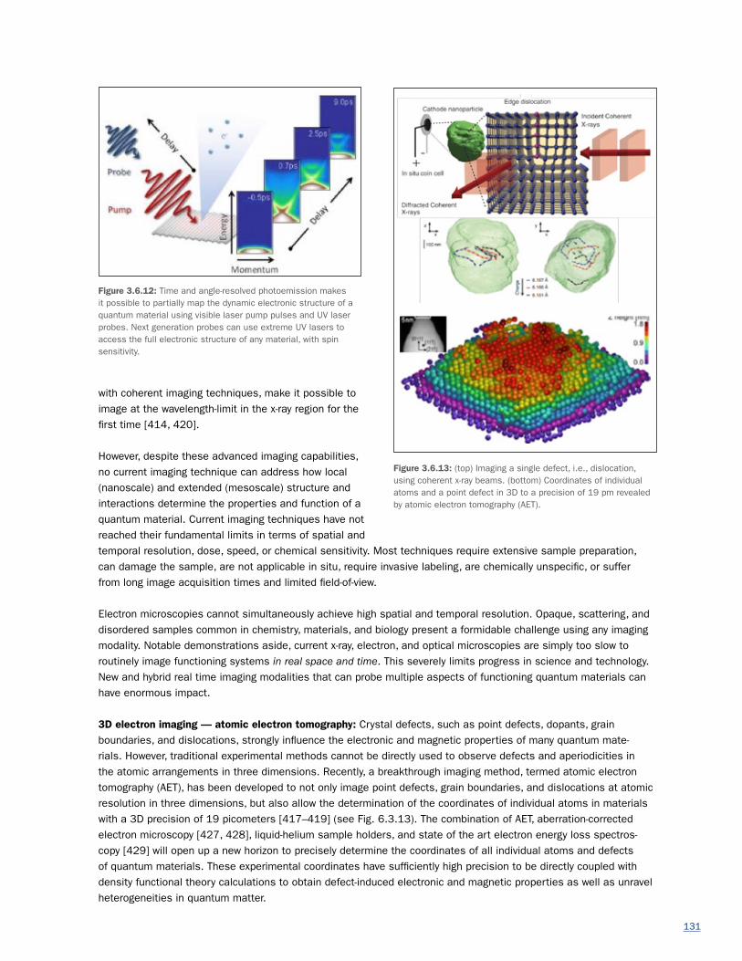
131
with coherent imaging techniques, make it possible to image at the wavelength-limit in the x-ray region for the first time [414, 420].
However, despite these advanced imaging capabilities, no current imaging technique can address how local (nanoscale) and extended (mesoscale) structure and interactions determine the properties and function of a quantum material. Current imaging techniques have not reached their fundamental limits in terms of spatial and temporal resolution, dose, speed, or chemical sensitivity. Most techniques require extensive sample preparation, can damage the sample, are not applicable in situ, require invasive labeling, are chemically unspecific, or suffer from long image acquisition times and limited field-of-view.
Electron microscopies cannot simultaneously achieve high spatial and temporal resolution. Opaque, scattering, and disordered samples common in chemistry, materials, and biology present a formidable challenge using any imaging modality. Notable demonstrations aside, current x-ray, electron, and optical microscopies are simply too slow to routinely image functioning systems in real space and time. This severely limits progress in science and technology. New and hybrid real time imaging modalities that can probe multiple aspects of functioning quantum materials can have enormous impact.
3D electron imaging — atomic electron tomography: Crystal defects, such as point defects, dopants, grain boundaries, and dislocations, strongly influence the electronic and magnetic properties of many quantum mate-rials. However, traditional experimental methods cannot be directly used to observe defects and aperiodicities in the atomic arrangements in three dimensions. Recently, a breakthrough imaging method, termed atomic electron tomography (AET), has been developed to not only image point defects, grain boundaries, and dislocations at atomic resolution in three dimensions, but also allow the determination of the coordinates of individual atoms in materials with a 3D precision of 19 picometers [417–419] (see Fig. 6.3.13). The combination of AET, aberration-corrected electron microscopy [427, 428], liquid-helium sample holders, and state of the art electron energy loss spectros-copy [429] will open up a new horizon to precisely determine the coordinates of all individual atoms and defects of quantum materials. These experimental coordinates have sufficiently high precision to be directly coupled with density functional theory calculations to obtain defect-induced electronic and magnetic properties as well as unravel heterogeneities in quantum matter.
Figure 3.6.12: Time and angle-resolved photoemission makes it possible to partially map the dynamic electronic structure of a quantum material using visible laser pump pulses and UV laser probes. Next generation probes can use extreme UV lasers to access the full electronic structure of any material, with spin sensitivity.
Figure 3.6.13: (top) Imaging a single defect, i.e., dislocation, using coherent x-ray beams. (bottom) Coordinates of individual atoms and a point defect in 3D to a precision of 19 pm revealed by atomic electron tomography (AET).
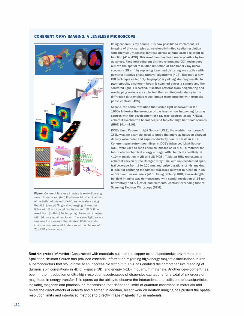
132
Neutron probes of matter: Constructed with materials such as the copper oxide superconductors in mind, the Spallation Neutron Source has provided essential information regarding high-energy magnetic fluctuations in iron superconductors that would have been inaccessible without it. This has enabled the comprehensive mapping of dynamic spin correlations in 4D of k-space (3D) and energy (+1D) in quantum materials. Another development has been in the introduction of ultra-high resolution spectroscopy of dispersive excitations for a total of six orders of magnitude in energy transfer. This opens up the ability to observe the interactions and collisions of quasiparticles, including magnons and phonons, on mesoscales that define the limits of quantum coherence in materials and reveal the direct effects of defects and disorder. In addition, recent work on neutron imaging has pushed the spatial resolution limits and introduced methods to directly image magnetic flux in materials.
COHERENT X-RAY IMAGING: A LENSLESS MICROSCOPE
Using coherent x-ray beams, it is now possible to implement 3D imaging of thick samples at wavelength-limited spatial resolution with chemical/magnetic contrast, across all time scales relevant to function [414, 420]. This revolution has been made possible by two advances. First, new coherent diffractive imaging (CDI) techniques remove the spatial resolution limitation of traditional x-ray micro-scopes (≈ 25 nm) by replacing lossy and distorting x-ray optics with powerful iterative phase retrieval algorithms [423]. Recently, a new CDI technique called “ptychography” is yielding stunning results. In ptychography, a coherent beam is scanned across a sample and the scattered light is recorded. If scatter patterns from neighboring and overlapping regions are collected, the resulting redundancy in the diffraction data enables robust image reconstruction with exquisite phase contrast [425].
Second, the same revolution that visible light underwent in the 1960s following the invention of the laser is now happening for x-ray sources with the development of x-ray free electron lasers (XFELs), coherent synchrotron beamlines, and tabletop high harmonic sources (HHG) [414–416].
DOE’s Linac Coherent Light Source (LCLS), the world’s most powerful XFEL, was, for example, used to probe the interplay between charged density wave order and superconductivity near 30 Tesla in YBCO. Coherent synchrotron beamlines at DOE’s Advanced Light Source (ALS) were used to map chemical phases of LiFePO4, a material for future electrochemical energy storage, with chemical specificity at <10nm resolution in 2D and 3D [426]. Tabletop HHG represents a coherent version of the Röntgen x-ray tube with unprecedented spec-tral coverage from 1 to 100 nm, and pulse durations of ≈fs, making it ideal for capturing the fastest processes relevant to function in 2D or 3D quantum materials [415]. Using tabletop HHG, at-wavelength, full-field imaging was demonstrated with spatial resolution of 14 nm horizontally and 5 Å axial, and elemental contrast exceeding that of Scanning Electron Microscopy (SEM).
Figure: Coherent lensless imaging is revolutionizing x-ray microscopes. (top) Ptychographic chemical map of partially delithiated LiFePO4 nanocrystals using the ALS. (center) Single shot imaging of nanopar-ticles with 5 nm spatial resolution and 10 fs time resolution. (bottom) Tabletop high harmonic imaging with 14 nm spatial resolution. The same light source was used to measure the shortest lifetime state in a quantum material to date — with a lifetime of 212±30 attoseconds.

133
3.6.3 Theory and Modeling
The past few years have seen a number of dramatic successes for the theory of quantum materials. Close con-nections between theory and experiment are a hallmark of quantum materials research, as the preceding sections make clear. It is worth remembering, however, that just as experiments are enabled by instrumentation and tech-nique development, theory also builds on methods and concepts whose immediate utility for understanding experi-ments is not always obvious.
For example, the theory of topological insulators, which made specific successful predictions about materials, built on topological concepts that were developed in the 1980s by workers such as Thouless and Haldane and might have seemed somewhat abstract or formal until recently. An older example is the classification of crystalline space groups in the nineteenth century, which greatly influenced solid-state physics once it became clear how to use Bragg scattering to reveal crystal structures.
This section is concerned with theoretical developments that ultimately enable our ability to make predictions about specific materials and experiments. These range from concepts and analytical methods to a variety of computational and modeling capabilities. New instrumentation and new classes of materials both create major challenges for the-ory, and without corresponding improvements in our theoretical knowledge base, the field could revert to a collection of observations and demonstrations without a high level of understanding.
Current status and recent advances: Let us start with the 1980s, as that decade represented the beginning for several of the research areas in this report. The discovery of cuprate and heavy fermion superconductors revealed that new materials classes could support new superconducting orders (e.g., p-, f-, and d-wave rather than s-wave) via new “strong correlation” mechanisms and with potentially useful advantages. The discovery of the quantum Hall effect and its rapid theoretical explanation made it clear that, at least under extreme conditions of low tempera-ture, high magnetic field, and low dimensionality, there were kinds of quantum matter that were not captured by the Landau-Ginzburg-Wilson paradigm of symmetry breaking.
Considerable insight into both these areas has occurred in recent years. The cuprates and other unconventional superconductors turn out to support a plethora of other kinds of charge, spin, and orbital order, and understanding the experimental consequences of these has been a major area of theory. A sophisticated theoretical framework capturing many different kinds of topological order has been developed in the past few years, and we know that topological phases are much more common and robust than suspected in the 1980s. In several cases the exper-imental observation of a new kind of topological phase or superconducting parameter took place only after it had been suggested/predicted by theory.
An example of how new computational approaches have improved our ability to study strongly correlated materials is provided by dynamical mean field theory (DMFT) [430]. The most widely used set of computational techniques for electronic properties of materials is based on a powerful set of ideas called density functional theory (DFT). While for many materials these ideas give accurate and efficiently scalable results, strong correlation has long been known to cause difficulties for them. DMFT increases the applicability of computation by incorporating correlation effects in a self-consistent way; while the spatial structure of the interaction is approximated, DMFT is able to capture correla-tion phenomena in many of the superconducting [431] and magnetic [432] materials discussed in this document and give accurate estimates of their phase diagram. It integrates well with DFT and is less computationally expen-sive than the full Hilbert space methods discussed as a frontier below.
Theoretical methods have also improved their ability to go beyond the low-energy, long-wavelength physics of sys-tems near equilibrium, where renormalization-group ideas mean that the description of even complicated systems can become quite simple. As experimental techniques were developed or improved (e.g., angle-resolved photoemis-sion and scanned probe measurements on correlated materials), corresponding theoretical advances took place as well. Numerical methods for strong correlation problems have improved vastly in the past two decades: We appear to be nearing convergence on the ground-state phase diagram of the Hubbard model, which is an idealized

134
description of the cuprates, and even some fully quantum dynamical problems are now tractable. Our understanding of quantum materials is far from perfect, however, and some long-standing challenges are discussed in the following section along with new problems and opportunities.
Scientific challenges and opportunities: Quantum materials continue to present “mysteries” for theory that keep the field scientifically exciting. Most quantum materials have significant electronic correlations and, as a result, we do not yet have an automated genome-type process that, given a chemical formula, will predict its stable form(s) in the solid state and their important electronic properties. Even at the qualitative or phenomenological level, there are aspects of complex superconductors and magnets that we do not yet fully understand. Examples are the nature of quantum critical points with itinerant fermions; the types of spin liquid that may be realized in frustrated magnets; and universality in far-from-equilibrium quantum dynamics and the origin of dissipation/damping.
The nature of transport in materials ranging from graphene to correlated 3D crystals may be better described, when the materials are clean and strongly interacting, by a hydrodynamical picture rather than nearly free electrons scat-tering off impurities. New kinds of hydrodynamics and new bounds on hydrodynamical quantities such as viscosity have been an active area in both condensed matter and high-energy physics in the past decade. Simple hydrody-namical models (including classical differential equations for densities and currents like time-dependent Ginsburg-Landau theory) are already used to model far-from-equilibrium quantum dynamics, but the applicability of such models is debatable as the time and space scales resolved in experiments become shorter.
On the computational frontier, there are opportunities for better linkage between “all-electron” methods, like densi-ty-functional theory, that do not handle strong correlations well but are probably acceptably accurate for most of the electrons in a material, with strong-correlation methods that are computationally expensive. Recent work on combin-ing DFT with dynamical mean-field theory in more complicated structures is an example of progress in this direction. These advances might help in coupling theory with synthesis and advanced spectroscopic data from ARPES and neutron scattering.
Density-matrix renormalization group (DMRG) is a very powerful method for treating correlations that has been advanced by ideas from quantum information. It can be nearly exact for some one-dimensional systems (both statics and dynamics) and 2D ground states, and can provide detailed information on the limits of DFT with various correlation functionals. Far-from-equilibrium physics is a challenge for computation as well as for analytical theory, but again progress is happening and a challenge may be to distribute that understanding so that more people are able to take advantage of it.
135
APPENDIX A: WORKSHOP PARTICIPANTS
Chair: Collin Broholm, Johns Hopkins UniversityCo-chairs: Ian R. Fisher, Stanford University
Joel E. Moore, LBNL/University of California, BerkeleyMargaret Murnane, University of Colorado, Boulder
Basic Energy Sciences Team:
Linda Horton, Jim Horwitz, Jim Davenport, Matthias Graf, Jeff Krause, Mick Pechan, Kelly Perry (ORNL detail to BES), Jim Rhyne, Thiyaga Thiyagarajan, Andrew Schwartz, and Katie Runkles (administrative)
Plenary Speakers:
Harold Hwang, SLAC National Accelerator Laboratory and Stanford University (5)Alessandra Lanzara, LBNL/University of California, Berkeley (3)Peter Littlewood, Argonne National LaboratoryStuart Parkin, Max Planck Institute of Microstructure Physics Subir Sachdev, Harvard UniversityLouis Taillefer, University of Sherbrooke (Quebec)Eli Yablonovitch, University of California, Berkeley
Panel 1: Superconductivity and Charge Order in Quantum Materials
Leads: Adriana Moreo, University of Tennessee, Knoxville and Oak Ridge National LaboratoryJohn Tranquada, Brookhaven National Laboratory
Peter Abbamonte, University of Illinois at Urbana-ChampaignGregory Boebinger, Florida State University (National High Magnetic Field Laboratory) (B)Pengcheng Dai, Rice UniversityChang Beom Eom, University of Wisconsin, MadisonRafael Fernandes, University of Minnesota Duane Johnson, Ames LaboratoryMercouri Kanatzidis, ANL/Northwestern University (A)Eun-Ah Kim, Cornell UniversityWai-Kwong Kwok, ANLAbhay Pasupathy, Columbia UniversityAthena Sefat, ORNLJoe Thompson, LANLNandini Trivedi, Ohio State University (C)
Note: (1), (2), (3), (4), and (5) indicate the theme panel that the individual represents. (A), (B), and (C) indicate the cross-cutting panel that the individual represents.
136
Panel 2: Magnetism and Spin in Quantum Materials
Leads: Meigan Aronson, Texas A&M UniversityAllan MacDonald, University of Texas, Austin
Sang-Wook Cheong, Rutgers University Piers Coleman, Rutgers UniversityClaudia Felser, Max Planck Institute, Dresden (Germany)Frances Hellman, LBNL/University of California, BerkeleyAxel Hoffmann, ANLYoung June Kim, University of Toronto (Canada)Chris Marianetti, Columbia UniversityTyrel McQueen, Johns Hopkins University (A)Christian Pfleiderer, Technische Universität München (Germany)Oleg Tchernyshyov, Johns Hopkins UniversityAlan Tennant, ORNL (B) Yaroslav Tserkovnyak, University of California, Los AngelesSteve White, University of California, Irvine
Panel 3: Transport and Non-Equilibrium Dynamics in Quantum Materials
Leads: Dimitri Basov, University of California, San DiegoJim Freericks, Georgetown University
Luis Balicas, Florida State University (National High Magnetic Field Laboratory)Tom Devereaux, SLAC/Stanford University (C)Hermann Durr, SLAC/Stanford UniversityEric Fullerton, University of California, San DiegoNuh Gedik, Massachusetts Institute of TechnologyChris Hammel, Ohio State UniversityJames Hone, Columbia University (A)Alessandra Lanzara, LBNL/University of California, Berkeley (plenary speaker) (B)Jeanie Lau, University of California, RiversideCharles H. Mielke, LANL (National High Magnetic Field Laboratory)Joe Orenstein, LBNL/University of California, BerkeleyJohnpierre Paglione, University of MarylandTheo Rasing, Radboud University (Netherlands) Toni J. Taylor, LANL (B)
Panel 4: Topological Quantum Materials
Leads: Eduardo Fradkin, University of Illinois at Urbana-ChampaignAmir Yacoby, Harvard University
James Analytis, LBNL/University of California, BerkeleyN. Peter Armitage, Johns Hopkins UniversityAndrei Bernevig, Princeton University (C)Judy Cha, Yale University (A)Claudio Chamon, Boston UniversityLiang Fu, Massachusetts Institute of TechnologyDavid Goldhaber-Gordon, SLAC/Stanford UniversityVidya Madhavan, University of Illinois at Urbana-ChampaignLaurens Molenkamp, University of Wuerzburg (Germany)Emilia Morosan, Rice UniversityNai Phuan Ong, Princeton University (B)Dale J. Van Harlingen, University of Illinois at Urbana-ChampaignShoucheng Zhang, SLAC/Stanford University
137
Panel 5: Heterogeneous and Nano-Structured Quantum Materials
Leads: Nitin Samarth, Pennsylvania State UniversitySusanne Stemmer, University of California, Santa Barbara
David Awschalom, ANL/University of ChicagoGreg Fiete, University of Texas, Austin (C)Harold Hwang, SLAC/Stanford University (plenary speaker) (A)Ali Javey, LBNL/University of California, BerkeleyMike Manfra, Purdue UniversitySteve May, Drexel UniversityDoug Natelson, Rice UniversitySatoshi Okamoto, ORNLStuart Parkin, IBM and Max Planck Institute, Halle (Germany)Jie Shan, Pennsylvania State UniversityKyle Shen, Cornell University (B)Kang Wang, University of California, Los AngelesAndrea Young, University of California, Santa Barbara
Cross-Cutting Panel A: Synthesis
Lead: Ian Fisher, Stanford University/SLACJudy Cha, Yale University (4)Sang-Wook Cheong, Rutgers University (2)James Hone, Columbia University (3)Harold Hwang, SLAC/Stanford University (plenary speaker) (5)Mercouri Kanatzidis, ANL/Northwestern University (1)Tyrel McQueen, Johns Hopkins University (2)
Cross-Cutting Panel B: Instrumentation
Leads: Collin Broholm, Johns Hopkins UniversityMargaret Murnane, University of Colorado, Boulder
Gregory Boebinger, Florida State University (National High Magnetic Field Laboratory) (1)Alessandra Lanzara, LBNL/University of California, Berkeley (plenary speaker) (3)John Miao, University of California, Los Angeles (Instrumentation) Nai Phuan Ong, Princeton University (4)Markus Raschke, University of Colorado, BoulderKyle Shen, Cornell University (5)Toni J. Taylor, LANL (3)Alan Tennant, ORNL (2)
Cross-cutting Panel C: Theory and Modeling Lead: Joel Moore, LBNL/University of California, BerkeleyAndrei Bernevig, Princeton University (4)Tom Devereaux, SLAC/Stanford University (3)Greg Fiete, University of Texas, Austin (5)Nandini Trivedi, Ohio State University (1)Steve White, University of California, Irvine (2)
Note: (1), (2), (3), (4) and (5) indicate the theme panel that the individual represents. (A), (B), and (C) indicate the cross-cutting panel that the individual represents.

138
Basic Research Needs for Quantum Materials for Energy-relevant Technology Invited Participants (alphabetical)
Peter Abbamonte, University of Illinois at Urbana-ChampaignJames Analytis, LBNL/University of California, BerkeleyN. Peter Armitage, Johns Hopkins UniversityMeigan Aronson, Texas A&M UniversityDavid Awschalom, ANL/University of ChicagoLuis Balicas, Florida State University (National High Magnetic Field Laboratory)Dimitri Basov, University of California, San DiegoAndrei Bernevig, Princeton UniversityGregory Boebinger, Florida State University (National High Magnetic Field Laboratory)Collin Broholm, Johns Hopkins UniversityJudy Cha, Yale UniversityClaudio Chamon, Boston UniversitySang-Wook Cheong, Rutgers UniversityPiers Coleman, Rutgers UniversityPengcheng Dai, Rice UniversityTom Devereaux, SLAC/Stanford UniversityHermann Durr, SLAC/Stanford UniversityChang-Beom Eom, University of Wisconsin, MadisonClaudia Felser, Max Planck Institute, Dresden (Germany)Rafael Fernandes, University of MinnesotaGreg Fiete, University of Texas, AustinIan Fisher, Stanford University/SLACEduardo Fradkin, University of Illinois at Urbana-ChampaignJim Freericks, Georgetown UniversityLiang Fu, Massachusetts Institute of TechnologyEric Fullerton, University of California, San DiegoNuh Gedik, Massachusetts Institute of TechnologyDavid Goldhaber-Gordon, SLAC/Stanford UniversityChris Hammel, Ohio State UniversityFrances Hellman, LBNL/University of California, BerkeleyAxel Hoffmann, ANLJames Hone, Columbia UniversityHarold Hwang, SLAC/Stanford UniversityAli Javey, LBNL/University of California, BerkeleyDuane Johnson, Ames LaboratoryMercouri Kanatzidis, ANL/Northwestern UniversityEun-Ah Kim, Cornell UniversityYoung June Kim, University of Toronto (Canada)Wai-Kwong Kwok, ANLAlessandra Lanzara, LBNL/University of California, BerkeleyJeanie Lau, University of California, RiversidePeter Littlewood, ANLAllan MacDonald, University of Texas, AustinVidya Madhavan, University of Illinois at Urbana-ChampaignMike Manfra, Purdue UniversityChris Marianetti, Columbia UniversitySteve May, Drexel UniversityTyrel McQueen, Johns Hopkins UniversityJohn Miao, University of California, Los Angeles

139
Charles H. Mielke, LANL (National High Magnetic Field Laboratory)Laurens Molenkamp, University of Wuerzburg (Germany)Joel Moore, LBNL/University of California, BerkeleyAdriana Moreo, University of Tennessee, Knoxville and Oak Ridge National LaboratoryEmilia Morosan, Rice UniversityMargaret Murnane, University of Colorado, BoulderDoug Natelson, Rice UniversitySatoshi Okamoto, ORNLNai-Phuan Ong, Princeton UniversityJoe Orenstein, LBNL/University of California, BerkeleyJohnpierre Paglione, University of MarylandStuart Parkin, IBM and Max Planck Institute, Halle (Germany)Abhay Pasupathy, Columbia UniversityChristian Pfleiderer, Technische Universität München (Germany)Markus Raschke, University of Colorado-Boulder Theo Rasing, Radboud University (Netherlands) Subir Sachdev, Harvard UniversityNitin Samarth, Pennsylvania State UniversityAthena Sefat, ORNLJie Shan, Pennsylvania State UniversityKyle Shen, Cornell UniversitySusanne Stemmer, University of California, Santa BarbaraLouis Taillefer, Université de Sherbrooke (Quebec, Canada)Toni J. Taylor, LANLOleg Tchernyshyov, Johns Hopkins UniversityAlan Tennant, ORNL Joe Thompson, LANLJohn Tranquada, Brookhaven National LaboratoryNandini Trivedi, Ohio State UniversityYaroslav Tserkovnyak, University of California, Los AngelesDale J. Van Harlingen, University of Illinois at Urbana-ChampaignKang Wang, University of California, Los AngelesSteve White, University of California, IrvineEli Yablonovitch, University of California, BerkeleyAmir Yacoby, Harvard UniversityAndrea Young, University of California, Santa BarbaraShoucheng Zhang, SLAC/Stanford University
Basic Research Needs for Quantum Materials for Energy-relevant Technology Invited Observers (alphabetical)
Nathan Baker, Pacific Northwest National LaboratorySasha Balatsky, Los Alamos National LaboratoryMatt Beard, National Renewable Energy LaboratorySteve Binkley, DOE Office of Science, Advanced Scientific Computing ResearchBen Brown, DOE Office of ScienceTof Carim, Office of Science and Technology PolicyHans Christen, Oak Ridge National LaboratoryClaire Cramer, National Institute of Standards and TechnologyTeresa Crockett, DOE Office of Science, Basic Energy SciencesJim Davenport, DOE Office of Science, Basic Energy SciencesJonathan DuBois, Lawrence Livermore National Laboratory

140
Peter Fischer, Lawrence Berkeley National LaboratoryBonnie Gersten, DOE Office of Science, Basic Energy SciencesErnie Glover, Gordon and Betty Moore FoundationMatthias Graf, DOE Office of Science, Basic Energy SciencesRobin Hayes, DOE Office of Science, Basic Energy SciencesTing He, Idaho National LaboratoryLinda Horton, DOE Office of Science, Basic Energy SciencesJim Horwitz, DOE Office of Science, Basic Energy SciencesPeter Johnson, Brookhaven National LaboratoryMark Johnson, DOE Energy Efficiency and Renewable Energy, Advanced Manufacturing OfficeAdam Kaminsky, Ames LaboratoryHelen Kerch, DOE Office of Science, Basic Energy SciencesArvind Kini, DOE Office of Science, Basic Energy SciencesRefik Kortan, DOE Office of Science, Basic Energy SciencesJeff Krause, DOE Office of Science, Basic Energy SciencesHarriet Kung, DOE Office of Science, Basic Energy SciencesEliane Lessner, DOE Office of Science, Basic Energy SciencesMike Lilly, Sandia National LaboratoryGeorge Maracas, DOE Office of Science, Basic Energy SciencesGail McLean, DOE Office of Science, Basic Energy SciencesGlen McWright, Department of DefenseTalia Melcer, DOE Office of Science, Basic Energy SciencesJohn Mitchell, Argonne National LaboratoryMick Pechan, DOE Office of Science, Basic Energy SciencesKelly Perry, Oak Ridge National Laboratory on detail to DOE-Basic Energy SciencesRobinson Pino, DOE Office of Science, Advanced Scientific Computing ResearchKimberly Rasar, DOE Office of the Under Secretary for Science and Energy Jim Rhyne, DOE Office of Science, Basic Energy SciencesKatie Runkles, DOE Office of Science, Basic Energy SciencesThomas Russell, DOE Office of Science, Basic Energy SciencesReuben Sarkar, DOE Energy Efficiency and Renewable Energy, TransportationAndy Schwartz, DOE Office of Science, Basic Energy SciencesTom Settersten, DOE Office of Science, Basic Energy SciencesJim Siegrist, DOE Office of Science, High Energy PhysicsCeren Susut-Bennett, DOE Office of Science, Advanced Scientific Computing ResearchThiyaga Thiyagarajan, DOE Office of Science, Basic Energy SciencesJohn Vetrano, DOE Office of Science, Basic Energy SciencesLane Wilson, DOE Office of Science, Basic Energy SciencesJane Zhu, DOE Office of Science, Basic Energy SciencesRagaiy Zidan, Savanah River National Laboratory

141
APPENDIX B: WORKSHOP AGENDA
BASIC RESEARCH NEEDS WORKSHOP ON
Quantum Materials for Energy Relevant TechnologyGaithersburg Marriott Washingtonian Center • February 8 – 10, 2016Chair: Collin Broholm, Johns Hopkins UniversityCo-chairs: Ian R. Fisher, Stanford University
Joel E. Moore, LBNL/University of California, BerkeleyMargaret Murnane, University of Colorado, Boulder
MONDAY FEBRUARY 8, 2016
7:00 AM Breakfast
Opening Plenary Session (Salons E/F/G)
8:00 AMBES Welcome and Workshop ChargeHarriet Kung, Associate Director of Science for Basic Energy Sciences
8:15 AMChair Welcome and Workshop StructureCollin Broholm, Johns Hopkins University
8:30 AMThe Quantum Critical Point of Cuprate Superconductors Louis Taillefer, University of Sherbrooke, Quebec
9:10 AMAntiferromagnetism and High Temperature SuperconductivitySubir Sachdev, Harvard University
9:50 AM Break
10:20 AMArtificially Structured Quantum Materials Harold Hwang, SLAC National Accelerator Laboratory and Stanford University
11:00 AMUltrafast Momentum Dependent Spectroscopy of Quantum MaterialsAlessandra Lanzara, LBNL/University of California, Berkeley
11:40 AMWhy We Need To Replace the Transistor, and What Would Be the Newly Required Material Properties?Eli Yablonovitch, University of California, Berkeley
12:20 PM Working Lunch (Salons E/F/G)
1:10 PM Panel Introductions — Workshop Co-Chairs
1:30 PM Panel Sessions (Refreshments available from 3:00–4:00 PM)
Panel 1 — Superconductivity and Charge Order in Quantum Materials (Salon D)Adriana Moreo, University of Tennessee, Knoxville and Oak Ridge National Laboratory and John Tranquada, Brookhaven National Laboratory
Panel 2 — Magnetism and Spin in Quantum Materials (Salon C)Meigan Aronson, Texas A&M and Allan MacDonald, University of Texas, Austin
Panel 3 — Transport and Non-Equilibrium Dynamics in Quantum Materials (Salons A/B Dimitri Basov, University of California, San Diego and Jim Freericks, Georgetown University
Panel 4 — Topological Quantum Materials (Lakeside #1)Eduardo Fradkin, University of Illinois at Urbana-Champaign and Amir Yacoby, Harvard University
Panel 5 — Heterogeneous and Nano-Structured Quantum Materials (Lakeside #2)Nitin Samarth, Pennsylvania State University and Susanne Stemmer, University of California, Santa Barbara
5:30 PM Working Dinner — Panel discussions (continued)
9:00 PM Discussions end for the day

142
TUESDAY FEBRUARY 9, 2016
7:00 AM Breakfast
Plenary Session (Salons E/F/G)
8:00 AMQuantum Materials for Energy and Sustainability Peter Littlewood, Argonne National Laboratory
8:40 AMSpintronic Materials and Phenomena for Advanced MemoriesStuart Parkin, Max Planck Institute of Microstructure Physics
9:20 AM Break and move to panel sessions (Refreshments available from 9:20-10:20)
9:30 AM Panels meet for discussion/preparation of preliminary reports
10:10 AM Break and move to plenary room for panel reports (Salon E/F/G)
10:20 AM Report from Panel 1 — Superconductivity and Charge Order in Quantum Materials
10:40 AM Report from Panel 2 — Magnetism and Spin in Quantum Materials
11:00 AM Report from Panel 3 — Transport and Non-Equilibrium Dynamics in Quantum Materials
11:20 AM Report from Panel 4 — Topological Quantum Materials
11:40 AM Report from Panel 5 — Heterogeneous and Nano-Structured Quantum Materials
12:00 PM Working Lunch (Salons E/F/G) — Continued discussion of panel reports
1:30 PMPanel discussions (continued) — Cross-cutting panels meet in plenary roomSynthesis, Instrumentation, and Theory and Modeling(Refreshments available from 3:00-4:00 PM)
5:30 PM Working Dinner — Panel discussions (continued) and preparation for final panel reports
9:00 PM Discussions end for the day
WEDNESDAY, FEBRUARY 10, 2016
7:00 AM Breakfast
Plenary Session (Salons E/F/G)
8:00 AM Report from Panel 1 — Superconductivity and Charge Order in Quantum Materials
8:30 AM Report from Panel 2 — Magnetism and Spin in Quantum Materials
9:00 AM Report from Panel 3 — Transport and Non-Equilibrium Dynamics in Quantum Materials
9:30 AM Break
9:45 AM Report from Panel 4 - Topological Quantum Materials
10:15 AM Report from Panel 5 - Heterogeneous and Nano-Structured Quantum Materials
10:45 AM Report from Cross-Cutting Panels (15 mins per crosscut)
11:30 AMClosing RemarksCollin Broholm, Johns Hopkins University
Writing Session (Lakeside #1/#2)
12:00 PM Working Lunch — Chairs, panel leads, and designated writers only
1:00 PM Writing — Chairs, panel leads, and designated writers
5:30 PM Dinner on your own

143
APPENDIX C: ABSTRACTS FOR PLENARY TALKS
The Quantum Critical Point of Cuprate Superconductors
Louis TailleferUniversity of Sherbrooke & Canadian Institute for Advanced Research
The origin of the exceptionally strong superconductivity found in copper oxide materials called cuprates remains one of the major puzzles in science. Because the critical temperature Tc for superconductivity peaks at a certain optimal concentration, it is believed that the electrons are controlled by an underlying critical point located at that concen-tration, where a quantum phase transition would occur. Identifying this quantum critical point has proven difficult because to do so unambiguously requires that the overlapping superconductivity be removed.
In this talk, I will describe some recent advances in our understanding of cuprates that came from suppressing superconductivity with very high magnetic fields, such as those produced by the French and American national labs. A clear signature of the quantum critical point has been detected, which points to antiferromagnetism as the funda-mental organizing principle.
I will touch on the crucial role of long-term international collaborations in achieving such advances, and describe how the Canadian Institute for Advanced Research has worked for the past 30 years to develop such collaborations in the field of quantum materials.
Antiferromagnetism and High-Temperature Superconductivity
Subir SachdevDepartment of Physics, Harvard University
It has long been known, from the example of liquid 3He, that weak magnetic fluctuations can mediate pairing between electrons, and lead to unconventional superconductivity. However, the question of whether the strong- coupling limit of such a theory can explain high-temperature superconductivity has proved much more difficult to answer. We now know, from both experiment and theory, that strong coupling leads to many remarkable new and unexpected phenomena: the appearance of charge density waves or other broken symmetries, strange metal phases without quasiparticle excitations, and possibly topological states with long-range quantum entanglement. I will survey recent progress on these issues, and also note the widespread impact on other areas of modern physics.
Artificially Structured Quantum Materials
Harold Y. HwangSLAC National Accelerator Laboratory, Stanford University
The ability to create and manipulate materials in low-dimensional form has repeatedly had transformative impact on science and technology. Recently, this trend has only accelerated along several approaches, such as exfoliation and assembly of intrinsically layered materials, and thin film growth of increasingly complex materials in atomic-scale heterostructures. These efforts have drawn particular attention to the opportunity to use the interfaces between quantum materials to engineer novel proximity effects and emergent phenomena. I will survey recent developments in this area, and suggest how they might be utilized in designing the physical and chemical properties of materials, both for fundamental research and for energy applications.

144
Ultra-Fast Momentum Dependent Spectroscopy of Quantum Materials
Alessandra LanzaraMaterials Science Division, Lawrence Berkeley National Laboratory
Physics Department, University of California, Berkeley
Spectroscopy, the art of studying interactions between light and matter, has been a driving force in physics back to the days of Newton. The latter half of the twentieth century, leading up to the present day, has seen a flourishing of activity driven first by the invention of the laser, and more recently by its transformation into commercialized turn-key systems that can generate trains of pulsed light at durations routinely less than 100 fs. These time scales are tech-nologically breathtaking if we think that a 100 fs time window is barely enough time for light to travel 30 microns. The real power lies in the fact that light reduced to sub-picosecond durations is opening new windows into the inter-actions between electrons in materials, which occur on precisely these time and energy scales. The prospect for this field is wide open and exciting. First experiments are revealing, to name a few, appearance of hidden phases that cannot exist in equilibrium, optical switch of spin and spin current, and control and enhancement of macroscopic properties through coherent and targeted light excitations.
I will present the recent progress of this field and the various directions where it is evolving, as well as discuss its impacts on other areas of modern physics.
Why We Need To Replace the Transistor, and What Would Be the Newly Required Material Properties?
Eli YablonovitchLawrence Berkeley National Laboratory, University of California, Berkeley
In contemplating the headlong rush toward miniaturization represented by Moore’s Law, it is tempting to think only of the progression toward molecular sized components. There is a second aspect of Moore’s Law that is sometimes overlooked. Owing to miniaturization, the energy efficiency of information processing has steadily improved.
But there is an inefficiency for internal communications in a chip. It is caused by the difference in voltage scale between the wires and the transistor switches. Transistors are thermally activated, leading to a required voltage >>kT/q. Wires are long, and they have a low impedance, allowing them to operate efficiently even at a few millivolts.Thus the main figure of merit for future transistors is low operating voltage or sensitivity, noy mobility.
The challenge then is to replace transistors with a new low-voltage switch that is better matched to the wires. I will present the new material quantum level properties, which are being explored by the NSF Science & Technology Center for Energy Efficient Electronics Science. http://www.e3s-center.org
Quantum Materials for Energy and Sustainability
Peter LittlewoodArgonne National Laboratory
Efficient and low-cost materials technologies are needed to support our transition to a sustainable planet. At the forefront will be progress in energy capture, storage, transmission, and use, as well as water management, distrib-uted sensing, and energy-efficient information technology. If our experience of the last century is any guide, evolving technologies will spawn new scientific questions and likely, whole new directions of enquiry.
While the big drivers for science and technology in recent decades have been the information society and the relentless progress to the nanoscale, many energy technologies need to be deployed on large scales and produce new functionality. In this talk, I will review some of the areas where there are clear technology needs, and assess opportunities for the impact of research in quantum materials.

145
Spintronic Materials and Phenomena for Advanced Memories
Stuart ParkinMax Planck Institute for Microstructure Physics
IBM Research-Almaden, San Jose, California
Recent advances in manipulating spin-polarized electron currents in atomically engineered magnetic heterostruc-tures make possible entirely new classes of sensor, memory, and logic devices — a research field generally referred to as spintronics. A magnetic recording read head, initially formed from a spin-valve, and more recently by a mag-netic tunnel junction, has enabled a 1,000-fold increase in the storage capacity of hard disk drives since 1997. The enormous storage capacity of arrays of hard disk drives in the “cloud” has made possible the digital storage and access to all of humankind’s knowledge since the beginning of mankind, thereby ushering in the age of “Big Data” and data analytics. The creation of unforeseen data-driven businesses and the transformation of entire industries is impacting society in manifold ways. Increasing the performance and reducing the energy consumption of storage and computing technologies will very likely spur yet more innovative applications of such technologies. Spintronic devices that rely on atomically engineered materials have novel properties that may allow for higher performance, lower energy, and more compact computing devices. As an example of the rich quantum physics that underlie spin-tronic devices, I discuss racetrack memory which is a novel three-dimensional technology that stores information as a series of magnetic domain walls in nanowires, manipulated by spin-polarized current. Racetrack memory is a spintronic technology that combines the low cost per stored bit of magnetic disk drives with the high performance and reliability of solid-state memories.
Key to the function of racetrack memory is the manipulation of magnetic moments via torques derived from spin currents, and the formation of chiral spin textures in the form of Néel domain walls and topological spin textures — skyrmions — stabilized by a Dzyaloshinskii-Moriya exchange interaction. Over the past few years there have been remarkable discoveries in the form of unexpectedly high efficiencies of charge to chiral spin current conversion via the spin Hall effect in both conventional metals and from topological spin textures. These spin currents lead to giant spin-orbit torques that have led to record-breaking current-induced domain wall speeds exceeding 1,000 m/sec in synthetic antiferromagnetic structures in which the net magnetization of the DWs is tuned to almost zero, making them “invisible.”

146
REFERENCES
1. Aristotle, de Anima. p. 405a 20–22.
2. Van Heddeghem, W., et al., Trends in worldwide ICT electricity consumption from 2007 to 2012. Computer Communications, 2014. 50: p. 64–76.
3. Anderson, P. W., The resonating valence bond state in La2CuO4 and superconductivity. Science, 1987. 235(4793): p. 1196–1198.
4. Mott, N.F., The transition to the metallic state. Philosophical Magazine, 1961. 6(62): p. 287–309.
5. Fradkin, E., S.A. Kivelson, and J.M. Tranquada, Colloquium: Theory of intertwined orders in high temperature
superconductors. Reviews of Modern Physics, 2015. 87(2): p. 457–482.
6. Gerber, S., et al., Switching of magnetic domains reveals spatially inhomogeneous superconductivity. Nature Physics, 2014. 10(2): p. 126–129.
7. Nandi, S., et al., Anomalous suppression of the orthorhombic lattice distortion in superconducting
Ba(Fe1-xCox)(2)As-2 Single Crystals. Physical Review Letters, 2010. 104(5): p. 057006.
8. Fernandes, R.M., A.V. Chubukov, and J. Schmalian, What drives nematic order in iron-based superconductors? Nature Physics, 2014. 10(2): p. 97–104.
9. Akahoshi, D., et al., Random potential effect near the bicritical region in perovskite manganites as revealed by
comparison with the ordered perovskite analogs. Physical Review Letters, 2003. 90(17): p.177203.
10. Kim, Y.K., et al., Observation of a d-wave gap in electron-doped Sr2IrO4. Nature Physics, 2016. 12(1): p. 37–42.
11. Han, T.H., et al., Fractionalized excitations in the spin-liquid state of a kagome-lattice antiferromagnet. Nature, 2012. 492(7429): p. 406–410.
12. Xu, S.Y., et al., Discovery of a Weyl fermion semimetal and topological Fermi arcs. Science, 2015. 349(6248): p. 613–617.
13. Lv, B.Q., et al., Experimental discovery of Weyl semimetal TaAs. Physical Review X, 2015. 5(3): p. 031013.
14. Wan, X.G., et al., Topological semimetal and Fermi-arc surface states in the electronic structure of pyrochlore
iridates. Physical Review B, 2011. 83(20). p. 205101: p. 205101.
15. Burkov, A.A., and L. Balents, Weyl semimetal in a topological insulator multilayer. Physical Review Letters, 2011. 107(12): p. 127205.
16. Morris, D.J.P., et al., Dirac strings and magnetic monopoles in the spin ice Dy2Ti2O7. Science, 2009. 326(5951): p. 411–414.
17. Castelnovo, C., R. Moessner, and S.L. Sondhi, Magnetic monopoles in spin ice. Nature, 2008. 451(7174): p. 42–45.
18. Fennell, T., et al., Magnetic coulomb phase in the spin ice Ho2Ti2O7. Science, 2009. 326(5951): p. 415–417.
19. Jaubert, L.D.C., and P.C.W. Holdsworth, Signature of magnetic monopole and Dirac string dynamics in spin ice.
Nature Physics, 2009. 5(4): p. 258–261.
20. Ladak, S., et al., Direct observation of magnetic monopole defects in an artificial spin-ice system. Nature Physics, 2010. 6(5): p. 359–363.
21. Pan, L.D., et al., A measure of monopole inertia in the quantum spin ice Yb2Ti2O7. Nature Physics, 2016. 12(4): p. 361–U97.
22. Shores, M.P., et al., A structurally perfect S = (1)/(2) kagome antiferromagnet. Journal of the American Chemical Society, 2005. 127(39): p. 13462–13463.
147
23. Freedman, D.E., et al., Site specific x-ray anomalous dispersion of the geometrically frustrated kagome magnet,
herbertsmithite, ZnCu3(OH)(6)Cl-2. Journal of the American Chemical Society, 2010. 132(45): p. 16185–16190.
24. Mourigal, M., et al., Molecular quantum magnetism in LiZn2Mo3O8. Physical Review Letters, 2014. 112(2): p. 027202.
25. Sheckelton, J.P., et al., Possible valence-bond condensation in the frustrated cluster magnet LiZn2Mo3O8. Nature Materials, 2012. 11(6): p. 493–496.
26. L.S. Wu, W.J.G., I.A. Zaliznyak, A.M. Tsvelik, J.S. Caux, M.S. Kim, Y. Qiu, J.R. Copley, G. Ehlers, A. Podlesnyak, M.C. Aronson, Orbital-exchange and fractional quantum number excitations on Ising spin ladders in Yb2Pt2Pb. Science, 2016. To appear.
27. Tokiwa, Y., et al., Quantum criticality in a metallic spin liquid. Nature Materials, 2014. 13(4): p. 356–359.
28. Ross, K.A., et al., Order by disorder spin wave gap in the XY pyrochlore magnet Er2Ti2O7. Physical Review Letters, 2014. 112(5): p. 057201.
29. Hallas, A.M., et al., Universal dynamic magnetism in Yb pyrochlores with disparate ground states. Physical Review B, 2016. 93(10): p. 100403.
30. Abd-Elmeguid, M.M., et al., Transition from Mott insulator to superconductor in GaNb4Se8 and GaTa4Se8 under
high pressure. Physical Review Letters, 2004. 93(12): p. 126403.
31. He, H., W. Miiller, and M.C. Aronson, New Kagome metal Sc3Mn3Al7Si5 and its gallium–doped analogues: synthe-
sis, crystal structure, and physical properties. Inorganic Chemistry, 2014. 53(17): p. 9115–9121.
32. Y. Tokiwa, C.S., M.S. Kim, T. Takabatake, P. Gegenwart, Characteristic signatures of quantum criticality driven by
geometric frustration. Science Advances, 2015. 1: p. e1500001.
33. Dzero, M., et al., Topological Kondo insulators. Physical Review Letters, 2010. 104(10): p. 106408.
34. Weng, H.M., et al., Topological crystalline Kondo insulator in mixed valence ytterbium borides. Physical Review Letters, 2014. 112(1): p. 016403.
35. Jiang, J., et al., Observation of possible topological in-gap surface states in the Kondo insulator SmB6 by photo-
emission. Nature Communications, 2013. 4: p. 3010.
36. Kim, D.J., J. Xia, and Z. Fisk, Topological surface state in the Kondo insulator samarium hexaboride. Nature Materials, 2014. 13(5): p. 466–470.
37. Li, G., et al., Two-dimensional Fermi surfaces in Kondo insulator SmB6. Science, 2014. 346(6214): p. 1208–1212.
38. Tan, B.S., et al., Unconventional Fermi surface in an insulating state. Science, 2015. 349(6245): p. 287–290.
39. Dzero, M., et al., Topological Kondo insulators. Annual review of condensed matter. Physics, Vol 7, 2016. 7: p. 249–280.
40. Okawa, M., et al., Hybridization gap formation in the Kondo insulator YbB12 observed using time-resolved photo-
emission spectroscopy. Physical Review B, 2015. 92(16): p. 161108.
41. Slebarski, A., and J. Spalek, From Kondo semimetal to spin-glass behaviour in doped CeNi1-delta Sn1+delta-
xSbx system. Philosophical Magazine, 2009. 89(22–24): p. 1845–1859.
42. Po-Yao Chang, O.E., Piers Coleman, Mobius Kondo Insulators. ArXiv, 2016. 1603.03435.
43. Li, T., et al., Gapped spin-liquid phase in the J(1)-J(2) Heisenberg model by a bosonic resonating valence-bond
ansatz. Physical Review B, 2012. 86(7): p. 075111.
44. Jiang, H.C., H. Yao, and L. Balents, Spin liquid ground state of the spin-1/2 square J(1)-J(2) Heisenberg model. Physical Review B, 2012. 86(2): p. 024424.
45. Gong, S.S., et al., Plaquette ordered phase and quantum phase diagram in the spin-1/2 j(1)-j(2) square
Heisenberg model. Physical Review Letters, 2014. 113(2): p. 027201.
46. Sekine, A., and K. Nomura, Axionic antiferromagnetic insulator phase in a correlated and spin-orbit coupled
system. Journal of the Physical Society of Japan, 2014. 83(10): p. 57-82.
148
47. Witczak-Krempa, W., et al., Correlated quantum phenomena in the strong spin-orbit regime. Annual Review of Condensed Matter Physics, Vol 5, 2014. 5: p. 57–82.
48. Jackeli, G. and G. Khaliullin, Mott insulators in the strong spin-orbit coupling limit: from Heisenberg to a quantum
compass and Kitaev models. Physical Review Letters, 2009. 102(1): p. 161108.
49. Plumb, K.W., et al., alpha-RuCl3: A spin-orbit assisted Mott insulator on a honeycomb lattice. Physical Review B, 2014. 90(4): p. 041112.
50. Kitaev, A., Anyons in an exactly solved model and beyond. Annals of Physics, 2006. 321(1): p. 2–111.
51. Kim, B.J., et al., Novel J(eff)=1/2 Mott state induced by relativistic spin-orbit coupling in Sr2IrO4. Physical Review Letters, 2008. 101(7): p. 076402.
52. Khaliullin, G., Excitonic magnetism in Van Vleck-type d(4) Mott insulators. Physical Review Letters, 2013. 111(19): p. 197201.
53. Shimizu, Y., et al., Spin liquid state in an organic Mott insulator with a triangular lattice. Physical Review Letters, 2003. 91(10): p. 107001.
54. Isono, T., et al., Gapless quantum spin liquid in an organic spin-1/2 triangular-lattice kappa — H-3(Cat-EDT-TTF)(2). Physical Review Letters, 2014. 112(17): p. 177201.
55. Yan, S.M., D.A. Huse, and S.R. White, Spin-liquid ground state of the s=1/2 kagome Heisenberg antiferromag-
net. Science, 2011. 332(6034): p. 1173–1176.
56. Wan, Y., and O. Tchernyshyov, Phenomenological Z(2) lattice gauge theory of the spin-liquid state of the kagome
Heisenberg antiferromagnet. Physical Review B, 2013. 87(10): p. 104408.
57. Hickey, C., et al., Haldane-Hubbard Mott insulator: from tetrahedral spin crystal to chiral spin liquid. Physical Review Letters, 2016. 116(13): p. 137–202.
58. Bombin, H., Topological order with a twist: ising anyons from an abelian model. Physical Review Letters, 2010. 105(3): p. 030403.
59. Kitaev, A.Y., Fault-tolerant quantum computation by anyons. Annals of Physics, 2003. 303(1): p. 2–30.
60. Ryu, S., et al., Topological insulators and superconductors: tenfold way and dimensional hierarchy. New Journal of Physics, 2010. 12. p: 065010.
61. Kitaev, A., Periodic table for topological insulators and superconductors. AIP Conf. Proc., 2009. 1134: p. 22.
62. Read, N., and D. Green, Paired states of fermions in two dimensions with breaking of parity and time-reversal
symmetries and the fractional quantum Hall effect. Physical Review B, 2000. 61(15): p. 10267–10297.
63. Kitaev, A., Unpaired Majorana fermions in quantum wires. Physics Uspekhi, 2000. 44: p. 131.
64. Qi, X.L., et al., Time-reversal-invariant topological superconductors and superfluids in two and three dimensions. Physical Review Letters, 2009. 102(18): p. 187001.
65. Roy, R., Topological superfluids with time reversal symmetry. ArXiv, 2008. 0803.2868.
66. Sasaki, S., et al., Topological Superconductivity in CuxBi2Se3. Physical Review Letters, 2011. 107(21): p. 217001.
67. Sato, M. and S. Fujimoto, Existence of majorana fermions and topological order in nodal superconductors with
spin-orbit interactions in external magnetic fields. Physical Review Letters, 2010. 105(21): p. 217001.
68. Maeno, Y., et al., Evaluation of spin-triplet superconductivity in Sr2RuO4. Journal of the Physical Society of Japan, 2012. 81(1): p. 011009.
69. Kashiwaya, S., et al., Edge states of Sr2RuO4 detected by in-plane tunneling spectroscopy. Physical Review Letters, 2011. 107(7): p. 077003.
70. Cho, G.Y., and J.E. Moore, Topological BF field theory description of topological insulators. Annals of Physics, 2011. 326(6): p. 1515–1535.
71. Chan, A., et al., Effective field theories for topological insulators by functional bosonization. Physical Review B, 2013. 87(8): p. 085132.
72. Wang, C., A.C. Potter, and T. Senthil, Classification of interacting electronic topological insulators in three dimen-
sions. Science, 2014. 343(6171): p. 629–631.
149
73. Wang, C., and T. Senthil, Interacting fermionic topological insulators/superconductors in three dimensions.
Physical Review B, 2014. 89(19): p. 195124.
74. Pesin, D., and L. Balents, Mott physics and band topology in materials with strong spin-orbit interaction. Nature Physics, 2010. 6(5): p. 376–381.
75. Chaloupka, J., G. Jackeli, and G. Khaliullin, Kitaev-Heisenberg model on a honeycomb lattice: possible exotic
phases in iridium oxides A(2)IrO(3). Physical Review Letters, 2010. 105(2): p. 027204.
76. Witczak-Krempa, W., and Y.B. Kim, Topological and magnetic phases of interacting electrons in the pyrochlore
iridates. Physical Review B, 2012. 85(4): p. 045124.
77. Fang, C., M.J. Gilbert, and B.A. Bernevig, Topological insulators with commensurate antiferromagnetism.
Physical Review B, 2013. 88(8): p. 085406.
78. Mong, R.S.K., A.M. Essin, and J.E. Moore, Antiferromagnetic topological insulators. Physical Review B, 2010. 81(24): p. 245209.
79. Sikkema, A.E., I. Affleck, and S.R. White, Spin gap in a doped Kondo chain. Physical Review Letters, 1997. 79(5): p. 929–932.
80. Zachar, O., and A.M. Tsvelik, One-dimensional electron gas interacting with a Heisenberg spin-1/2 chain.
Physical Review B, 2001. 64(3): p. 1559-1562.
81. Berg, E., E. Fradkin, and S.A. Kivelson, Pair-density-wave correlations in the Kondo-Heisenberg model. Physical Review Letters, 2010. 105(14): p. 146403.
82. Cho, G.Y., R. Soto-Garrido, and E. Fradkin, Topological pair-density-wave superconducting states. Physical Review Letters, 2014. 113(25): p. 256405.
83. Tsui, D.C., H.L. Stormer, and A.C. Gossard, Two-dimensional magnetotransport in the extreme quantum limit.
Physical Review Letters, 1982. 48(22): p. 1559–1562.
84. Laughlin, R.B., Anomalous quantum Hall effect — an incompressible quantum fluid with fractionally charged
excitations. Physical Review Letters, 1983. 50(18): p. 1395–1398.
85. Halperin, B.I., Statistics of quasiparticles and the hierarchy of fractional quantized hall states. Physical Review Letters, 1984. 52(18): p. 1583–1586.
86. Wen, X.G., Quantum field theory of many body systems. 2003: Cambridge University Press.
87. Fradkin, E., Field theories of condensed matter systems. 2013: Cambridge University Press.
88. Wen, X.G., Topological orders and edge excitations in fractional quantum Hall states. Advances in Physics, 1995. 44(5): p. 405–473.
89. Levin, M., and A. Stern, Fractional topological insulators. Physical Review Letters, 2009. 103(19): p. 196803.
90. Neupert, T., et al., Fractional (Chern and topological) insulators. Physica Scripta, 2015. T164: p. 014005.
91. Stern, A., Fractional topological insulators: a pedagogical review. Annual Review of Condensed Matter Physics, Vol 7, 2016. 7: p. 349–368.
92. L. Savary, L.B., Quantum spin liquids. ArXiv, 2016. arXiv:1601.03742v1.
93. Sheng, D.N., et al., Fractional quantum Hall effect in the absence of Landau levels. Nature Communications, 2011. 2: p. 389.
94. Neupert, T., et al., Fractional quantum hall states at zero magnetic field. Physical Review Letters, 2011. 106(23): p. 236804.
95. Jackson, T.S., G. Moller, and R. Roy, Geometric stability of topological lattice phases. Nature Communications, 2015. 6. p: 8629.
96. Xu, Y., et al., Large-gap quantum spin hall insulators in tin films. Physical Review Letters, 2013. 111(13): p. 136804.
97. Cirac, J.I., and F. Verstraete, Renormalization and tensor product states in spin chains and lattices. Journal of Physics a-Mathematical and Theoretical, 2009. 42(50): p. 504004.

150
98. White, S.R., Density-matrix formulation for quantum renormalization-groups. Physical Review Letters, 1992. 69(19): p. 2863–2866.
99. Hallberg, K.A., New trends in density matrix renormalization. Advances in Physics, 2006. 55(5–6): p. 477–526.
100. Schollwock, U., The density-matrix renormalization group in the age of matrix product states. Annals of Physics, 2011. 326(1): p. 96–192.
101. Teo, J.C.Y., and C.L. Kane, From Luttinger liquid to non-Abelian quantum Hall states. Physical Review B, 2014. 89(8): p. 085101.
102. Mong, R.S.K., et al., Universal topological quantum computation from a superconductor-Abelian quantum hall
heterostructure. Physical Review X, 2014. 4(1): p. 011036.
103. Ando, Y., Topological insulator materials. Journal of the Physical Society of Japan, 2013. 82(10): p. 102001.
104. Marcinkova, A., et al., Topological metal behavior in GeBi2Te4 single crystals. Physical Review B, 2013. 88(16): p. 710–712.
105. Chu, J.H., et al., Divergent nematic susceptibility in an iron arsenide superconductor. Science, 2012.337(6095): p. 710–712.
106. Zhao, L., et al., Evidence of an odd-parity hidden order in a spin-orbit coupled correlated iridate. Nature Physics, 2016. 12(1): p. 32-36.
107. Qi, X.L., T.L. Hughes, and S.C. Zhang, Topological field theory of time-reversal invariant insulators. Physical Review B, 2008. 78(19): p. 195424.
108. Essin, A.M., J.E. Moore, and D. Vanderbilt, Magnetoelectric polarizability and axion electrodynamics in crystal-
line insulators. Physical Review Letters, 2009. 102(14): p. 146805.
109. Fiebig, M., Revival of the magnetoelectric effect. Journal of Physics D-Applied Physics, 2005. 38(8): p. R123–R152.
110. Dzyaloshinskii, I.E., On the magneto-electrical effect in antiferromagnets. Soviet Physics Jetp-Ussr, 1960. 10(3): p. 628–629.
111. Wang, J., et al., Epitaxial BiFeO3 multiferroic thin film heterostructures. Science, 2003. 299(5613): p. 1719–1722.
112. Wu, L., M.S., N. Koirala, J. Moon, S. Oh, N. P. Armitage, Quantized Faraday and Kerr rotation and axion electro-
dynamics of the surface states of the three-dimensional topological insulators. ArXiv, 2016. 1603.04317.
113. Swingle, B., et al., Correlated topological insulators and the fractional magnetoelectric effect. Physical Review B, 2011. 83(19): p. 385-388.
114. Maciejko, J., and G.A. Fiete, Fractionalized topological insulators. Nature Physics, 2015. 11(5): p. 385–388.
115. Maciejko, J., et al., Fractional topological insulators in three dimensions. Physical Review Letters, 2010. 105(24): p. 246809.
116. Wilczek, F., Magnetic-Flux, Angular-momentum, and statistics. Physical Review Letters, 1982. 48(17): p. 1144–1146.
117. Moore, G., and N. Read, Nonabelions in the fractional quantum Hall effect. Nuclear Physics B, 1991. 360(2–3): p. 362–396.
118. Nayak, C., et al., Non-Abelian anyons and topological quantum computation. Reviews of Modern Physics, 2008. 80(3): p. 1083–1159.
119. Wen, X.G., and Q. Niu, Ground-state degeneracy of the fractional quantum hall states in the presence of a ran-
dom potential and on high-genus riemann surfaces. Physical Review B, 1990. 41(13): p. 9377–9396.
120. Ivanov, D.A., Non-abelian statistics of half-quantum vortices in p-wave superconductors. Physical Review Letters, 2001. 86(2): p. 268–271.
121. Sau, J.D., et al., Generic new platform for topological quantum computation using semiconductor heterostruc-
tures. Physical Review Letters, 2010. 104(4): p. 040502.
151
122. Mourik, V., et al., Signatures of majorana fermions in hybrid superconductor-semiconductor nanowire devices. Science, 2012. 336(6084): p. 1003–1007.
123. Fu, L., and C.L. Kane, Probing neutral majorana fermion edge modes with charge transport. Physical Review Letters, 2009. 102(21). p. 216403.
124. S. Hart, H.R., M. Kosowsky, G. Ben-Shach, P. Leubner, C. Brüne, H. Buhmann, L. W. Molenkamp, B. I. Halperin, A. Yacoby, Controlled finite momentum pairing and spatially varying order parameter in proximitized HgTe quan-
tum wells. ArXiv, 2015. 1509.02940.
125. Nadj-Perge, S., et al., Observation of Majorana fermions in ferromagnetic atomic chains on a superconductor.
Science, 2014. 346(6209): p. 602–607.
126. Alicea, J. and P. Fendley, Topological phases with parafermions: theory and blueprints. Annual Review of Condensed Matter Physics, Vol 7, 2016. 7: p. 119–139.
127. J. H. She, C.H.K., C. J. Fennie, M. J. Lawler, and E. A. Kim, Topological superconductivity in metal/quantum-
spin-ice heterostructures. ArXiv, 2016. arXiv:1603.02692.
128. Wan, Z., et al., Induced superconductivity in high-mobility two-dimensional electron gas in gallium arsenide
heterostructures. Nature Communications, 2015. 6: p. 7426.
129. Fidkowski, L., and A. Kitaev, Topological phases of fermions in one dimension. Physical Review B, 2011. 83(7): p. 075103.
130. Granger, G., J.P. Eisenstein, and J.L. Reno, Observation of chiral heat transport in the quantum hall regime.
Physical Review Letters, 2009. 102(8): p. 086803.
131. Bid, A., et al., Observation of neutral modes in the fractional quantum Hall regime. Nature, 2010. 466(7306): p. 585-590.
132. Martin, J., et al., Localization of fractionally charged quasi-particles. Science, 2004. 305(5686): p. 980–983.
133. Martin, J., et al., Observation of electron-hole puddles in graphene using a scanning single-electron transistor.
Nature Physics, 2008. 4(2): p. 144–148.
134. Grosfeld, E., B. Seradjeh, and S. Vishveshwara, Proposed Aharonov-Casher interference measurement of
non-Abelian vortices in chiral p-wave superconductors. Physical Review B, 2011. 83(10): p. 104513.
135. Willett, R.L., et al., Magnetic-field-tuned Aharonov-Bohm oscillations and evidence for non-abelian anyons at
nu=5/2. Physical Review Letters, 2013. 111(18): p. 186401.
136. Willett, R.L., L.N. Pfeiffer, and K.W. West, Measurement of filling factor 5/2 quasiparticle interference with
observation of charge e/4 and e/2 period oscillations. Proceedings of the National Academy of Sciences of the United States of America, 2009. 106(22): p. 8853–8858.
137. Fu, L., and C.L. Kane, Josephson, Current and noise at a superconductor/quantum-spin-Hall-insulator/super-
conductor junction. Physical Review B, 2009. 79(16): p. 161408.
138. Frano, A., Spin spirals and charge textures in transition-metal-oxide 47 heterostructures. 2014, Switzerland: Springer International Publishing.
139. Chaloupka, J., and G. Khaliullin, Orbital order and possible superconductivity in LaNiO3/LaMO3 superlattices.
Phys. Rev. Lett., 2008. 100(1): p. 016404.
140. Hansmann, P., et al., Turning a nickelate fermi surface into a cupratelike one through heterostructuring. Phys. Rev. Lett., 2009. 103(1): p. 016401.
141. Coleman, P., and A.J. Schofield, Quantum criticality. Nature, 2005. 433(7023): p. 226–229.
142. Ahn, C.H., et al., Electrostatic modification of novel materials. Rev. Mod. Phys., 2006. 78(4): p. 1185–1212.
143. Jeong, J., et al., Suppression of metal-insulator transition in VO2 by electric field-induced oxygen vacancy forma-
tion. Science, 2013. 339(6126): p. 1402–1405.
144. Kim, Y.K., et al., Fermi arcs in a doped pseudospin-1/2 Heisenberg antiferromagnet. Science, 2014. 345(6193): p. 187–190.

152
145. Wang, Q.Y., et al., Interface-induced high-temperature superconductivity in single unit-cell FeSe films on SrTiO3.
Chinese Physics Letters, 2012. 29(3): p. 037402.
146. Ge, J.F., et al., Superconductivity above 100 K in single-layer FeSe films on doped SrTiO3. Nat. Mater., 2015. 14(3): p. 285–289.
147. Yeats, A.L., et al., Persistent optical gating of a topological insulator. Sci. Adv., 2015. 1: p. e1500640.
148. Mak, K.F., et al., Atomically thin MoS2: a new direct-gap semiconductor. Phys. Rev. Lett., 2010. 105(13): p. 136805.
149. Terrones, H., F. Lopez-Urias, and M. Terrones, Novel hetero-layered materials with tunable direct band gaps by
sandwiching different metal disulfides and diselenides. Sci. Rep., 2013. 3: p. 1549.
150. Mak, K.F., and J. Shan, Photonics and optoelectronics of 2D semiconductor transition metal dichalcogenides.
Nat. Photonics, 2016. 10: p. 216–226.
151. Mak, K.F., et al., The valley Hall effect in MoS2 transistors. Science, 2014. 344(6191): p. 1489–1492.
152. Mellnik, A.R., et al., Spin-transfer torque generated by a topological insulator. Nature, 2014. 511(7510): p. 449–451.
153. Heinrich, B., et al., Dynamic exchange coupling in magnetic bilayers. Physical Review Letters, 2003. 90(18): p. 187601.
154. Tserkovnyak, Y., A. Brataas, and G.E.W. Bauer, Enhanced Gilber damping in thin ferromagnetic films. Physical Review Letters, 2002. 88(11): p. 117601.
155. Berger, L., Emission of spin waves by a magnetic multilayer traversed by a current. Physical Review B, 1996. 54(13): p. 9353–9358.
156. Slonczewski, J.C., Current-driven excitation of magnetic multilayers. Journal of Magnetism and Magnetic Materials, 1996. 159(1–2): p. L1–L7.
157. Ralph, D.C., and M.D. Stiles, Spin transfer torques. Journal of Magnetism and Magnetic Materials, 2008. 320(7): p. 1190–1216.
158. Adur, R., et al., Damping of confined modes in a ferromagnetic thin insulating film: angular momentum transfer
across a nanoscale field-defined interface. Physical Review Letters, 2014. 113(17): p. 176601.
159. Wang, H.L., et al., Antiferromagnonic spin transport from Y3Fe5O12 into NiO. Physical Review Letters, 2014. 113(9): p. 097202.
160. Chumak, A.V., et al., Magnon spintronics. Nature Physics, 2015. 11(6): p. 453–461.
161. Chumak, A.V., et al., Scattering of backward spin waves in a one-dimensional magnonic crystal. Applied Physics Letters, 2008. 93(2): p. 022508.
162. Kostylev, M., et al., Partial frequency band gap in one-dimensional magnonic crystals. Applied Physics Letters, 2008. 92(13): p. 132504.
163. Ding, J., M. Kostylev, and A.O. Adeyeye, Magnonic crystal as a medium with tunable disorder on a periodical
lattice. Physical Review Letters, 2011. 107(4): p. 047205.
164. Ding, J., M. Kostylev, and A.O. Adeyeye, Realization of a mesoscopic reprogrammable magnetic logic based on
a nanoscale reconfigurable magnonic crystal. Applied Physics Letters, 2012. 100(7): p. 073114.
165. Krawczyk, M., and D. Grundler, Review and prospects of magnonic crystals and devices with reprogrammable
band structure. Journal of Physics-Condensed Matter, 2014. 26(12): p. 123202.
166. Shindou, R., et al., Chiral spin-wave edge modes in dipolar magnetic thin films. Physical Review B, 2013. 87(17): p. 174402.
167. Shindou, R., et al., Topological chiral magnonic edge mode in a magnonic crystal. Physical Review B, 2013. 87(17): p. 174427.
168. Topp, J., et al., Making a reconfigurable artificial crystal by ordering bistable magnetic nanowires. Physical Review Letters, 2010. 104(20): p. 207205.

153
169. Heyderman, L.J., and R.L. Stamps, Artificial ferroic systems: novel functionality from structure, interactions and
dynamics. Journal of Physics-Condensed Matter, 2013. 25(36): p. 363201.
170. Ezio Iacocca, S.G., Robert L. Stamps, Olle Heinonen, Reconfigurable spin wave band structure of artificial
square spin ice. ArXiv, 2015. arXiv:1510.06385V2.
171. Tomiyoshi, S., and Y. Yamaguchi, Magnetic-structure and weak ferromagnetism of Mn3sn studied by polarized
neutron-diffraction. Journal of the Physical Society of Japan, 1982. 51(8): p. 2478–2486.
172. Brown, P.J., et al., Determination of the magnetic-structure of Mn3Sn using generalized neutron polarization
analysis. Journal of Physics-Condensed Matter, 1990. 2(47): p. 9409–9422.
173. Nagamiya, T., S. Tomiyoshi, and Y. Yamaguchi, Triangular spin configuration and weak ferromagnetism of
Mn3Sn and Mn3Ge. Solid State Communications, 1982. 42(5): p. 385–388.
174. Nakatsuji, S., N. Kiyohara, and T. Higo, Large anomalous Hall effect in a non-collinear antiferromagnet at room
temperature. Nature, 2015. 527(7577): p. 212–215.
175. Nagaosa, N., et al., Anomalous Hall effect. Reviews of Modern Physics, 2010. 82(2): p. 1539–1592.
176. Shindou, R., and N. Nagaosa, Orbital ferromagnetism and anomalous Hall effect in antiferromagnets on the
distorted fcc lattice. Physical Review Letters, 2001. 87(11): p. 116801.
177. Metalidis, G., and P. Bruno, Topological Hall effect studied in simple models. Physical Review B, 2006. 74(4): p. 045327.
178. Martin, I. and C.D. Batista, Itinerant electron-driven chiral magnetic ordering and spontaneous quantum Hall
effect in triangular lattice models. Physical Review Letters, 2008. 101(15). p. 156402.
179. Chen, H., Q. Niu, and A.H. MacDonald, Anomalous Hall effect arising from noncollinear antiferromagnetism.
Physical Review Letters, 2014. 112(1). p. 017205.
180. Sonin, E.B., Analogs of superfluid flows for spins and electron-hole pairs. Zhurnal Eksperimentalnoi I Teoreticheskoi Fiziki, 1978. 74(6): p. 2097–2111.
181. Sonin, E.B., Spin currents and spin superfluidity (vol 59 , pg 181, 2010). Advances in Physics, 2010. 59(4): p. 483–483.
182. Takei, S., et al., Superfluid spin transport through antiferromagnetic insulators. Physical Review B, 2014. 90(9): p. 094408.
183. Takei, S., and Y. Tserkovnyak, Superfluid spin transport through easy-plane ferromagnetic insulators. Physical Review Letters, 2014. 112(22): p. 227201.
184. Bender, S.A., et al., Dynamic phase diagram of dc-pumped magnon condensates. Physical Review B, 2014. 90(9): p. 094409.
185. Bender, S.A., R.A. Duine, and Y. Tserkovnyak, Electronic pumping of quasiequilibrium bose-einstein-condensed
magnons. Physical Review Letters, 2012. 108(24): p. 246601.
186. Konig, J., M.C. Bonsager, and A.H. MacDonald, Dissipationless spin transport in thin film ferromagnets.
Physical Review Letters, 2001. 87(18): p. 187202.
187. Pfleiderer, C., Magnetic order surfaces get hairy. Nature Physics, 2011. 7(9): p. 673–674.
188. Pfleiderer, C., and A. Rosch, Condensed-matter physics single skyrmions spotted. Nature, 2010. 465(7300): p. 880–881.
189. Xiao, D., et al., Coupled spin and valley physics in monolayers of $\mathrmmos_2$ and other group-vi
dichalcogenides. Physical Review Letters, 2012. 108(19): p. 196802.
190. Yao, W., D. Xiao, and Q. Niu, Valley-dependent optoelectronics from inversion symmetry breaking. Physical Review B, 2008. 77(23): p. 235406.
191. Xiao, D., W. Yao, and Q. Niu, Valley-contrasting physics in graphene: magnetic moment and topological trans-
port. Physical Review Letters, 2007. 99(23): p. 236809.
192. Akhmerov, A.R., and C.W.J. Beenakker, Detection of valley polarization in graphene by a superconducting con-
tact. Physical Review Letters, 2007. 98(15): p. 157003.
154
193. Rycerz, A., J. Tworzydlo, and C.W.J. Beenakker, Valley filter and valley valve in graphene. Nat Phys, 2007. 3(3): p. 172–175.
194. Lee, J., K.F. Mak, and J. Shan, Electrical control of the valley Hall effect in bilayer MoS2 transistors. Nat Nano, 2016. advance online publication.
195. Wang, L., et al., Evidence for a fractional fractal quantum Hall effect in graphene superlattices. Science, 2015. 350(6265): p. 1231–1234.
196. Dean, C.R., et al., Hofstadter’s butterfly and the fractal quantum Hall effect in moire superlattices. Nature, 2013. 497(7451): p. 598–602.
197. Fausti, D., et al., Light-induced superconductivity in a stripe-ordered cuprate. Science, 2011. 331(6014): p. 189–191.
198. Mankowsky, R., et al., Nonlinear lattice dynamics as a basis for enhanced superconductivity in YBa2Cu3O6.5.
Nature, 2014. 516(7529): p. 71–73.
199. Takesue, H., et al., Quantum teleportation over 100 km of fiber using highly efficient superconducting nanowire
single-photon detectors. Optica, 2015. 2(10): p. 832–835.
200. Wang, Y.H., et al., Observation of floquet-bloch states on the surface of a topological insulator. Science, 2013. 342(6157): p. 453–457.
201. Mahmood, F., et al., Selective scattering between Floquet-Bloch and Volkov states in a topological insulator.
Nature Physics, 2016. 12(4): p. 306–311.
202. Liu, T.M., et al., Nanoscale confinement of all-optical magnetic switching in tbfeco — competition with
nanoscale heterogeneity. Nano Letters, 2015. 15(10): p. 6862–6868.
203. Radu, I., et al., Transient ferromagnetic-like state mediating ultrafast reversal of antiferromagnetically coupled
spins. Nature, 2011. 472(7342): p. 205–208.
204. Wang, T.H., et al., Femtosecond single-shot imaging of nanoscale ferromagnetic order in Co/Pd multilayers
using resonant x-ray holography. Physical Review Letters, 2012. 108(26): p. 267403.
205. A. Boltasseva, V.M. Shalaev, All that glitters need not be gold. Science, 2014. 8: p. 1086–1101.
206. MacDonald, K.F., et al., Ultrafast active plasmonics. Nature Photonics, 2009. 3(1): p. 55–58.
207. Atwater, H.A., The promise of plasmonics. Scientific American, 2007. 296(4): p. 56–63.
208. Basov, D.N., et al., Colloquium: graphene spectroscopy. Reviews of Modern Physics, 2014. 86(3): p. 959–994.
209. Atkin, J.M., et al., Nano-optical imaging and spectroscopy of order, phases, and domains in complex solids.
Advances in Physics, 2012. 61(6): p. 745–842.
210. Wagner, M., et al., Ultrafast and nanoscale plasmonic phenomena in exfoliated graphene revealed by infrared
pump-probe nanoscopy. Nano Letters, 2014. 14(2): p. 894–900.
211. Wagner, M., et al., Ultrafast dynamics of surface plasmons in InAs by time-resolved infrared nanospectroscopy.
Nano Letters, 2014. 14(8): p. 4529–4534.
212. Ni, G.X., et al., Ultrafast optical switching of infrared plasmon polaritons in high-mobility graphene. Nature Photonics, 2016. 10(4): p. 244–247.
213. Weber, J.R., et al., Quantum computing with defects. Proceedings of the National Academy of Sciences of the United States of America, 2010. 107(19): p. 8513–8518.
214. Awschalom, D.D., et al., Quantum spintronics: engineering and manipulating atom-like spins in semiconductors.
Science, 2013. 339(6124): p. 1174–1179.
215. Dobrovitski, V.V., et al., Quantum control over single spins in diamond. Annual Review of Condensed Matter Physics, Vol 4, 2013. 4: p. 23–50.
216. P. V. Klimov, A.L.F., D. J. Christle, V. V. Dobrovitski, D. D. Awschalom, Quantum entanglement at ambient condi-
tions in a macroscopic solid-state spin ensemble. Science Advances, 2015. 1: p. e1501015.
217. Falk, A.L., et al., Optical polarization of nuclear spins in silicon carbide. Physical Review Letters, 2015. 114(24): p. 247603.

155
218. Bochmann, J., et al., Nanomechanical coupling between microwave and optical photons. Nature Physics, 2013. 9(11): p. 712–716.
219. Falk, A.L., et al., Polytype control of spin qubits in silicon carbide. Nature Communications, 2013. 4.
220. Fuchs, G.D., et al., Gigahertz dynamics of a strongly driven single quantum spin. Science, 2009. 326(5959): p. 1520–1522.
221. Banerjee, A., et al., Proximate Kitaev quantum spin liquid behaviour in a honeycomb magnet. Nature Materials, 2016. 15(7): p. 733–740.
222. Kang, K., et al., High-mobility three-atom-thick semiconducting films with wafer-scale homogeneity. Nature, 2015. 520(7549): p. 656–660.
223. Yu, Y.F., et al., Controlled scalable synthesis of uniform, high-quality monolayer and few-layer MoS2 films.
Scientific Reports, 2013. 3: p. 1866.
224. Li, X.S., et al., Synthesis of thin-film black phosphorus on a flexible substrate. 2d Materials, 2015. 2(3): p. 031002.
225. Phelan, W.A., et al., Stacking variants and superconductivity in the Bi-O-S system. Journal of the American Chemical Society, 2013. 135(14): p. 5372–5374.
226. Chamberland, B.l., Crystal growth of Cr02. Materials Research Bulletin, 1967. 2(9): p. 827.
227. Gardner, J.S., M.J.P. Gingras, and J.E. Greedan, Magnetic pyrochlore oxides. Reviews of Modern Physics, 2010. 82(1): p. 53–107.
228. Ketchum, D.R., and J.W. Kolis, Crystal growth of gallium nitride in supercritical ammonia. Journal of Crystal Growth, 2001. 222(3): p. 431–434.
229. H. Luo, K.Y., W. Xie, B. F. Phelan, R. J. Cava, Superconductivity in a misfit phase combining a topological crys-
talline insulator and a layered transition metal dichalcogenide. ArXiv, 2016. 1602.00018.
230. Kawaji, H., K. Hotehama, and S. Yamanaka, Superconductivity of alkali metal intercalated beta-zirconium
nitride chloride, A(x)ZrNCl (A = Li, Na, K). Chemistry of Materials, 1997. 9(10): p. 2127–2130.
231. Yamanaka, S., K. Hotehama, and H. Kawaji, Superconductivity at 25.5 K in electron-doped layered hafnium
nitride. Nature, 1998. 392(6676): p. 580–582.
232. Ran, Y., Y. Zhang, and A. Vishwanath, One-dimensional topologically protected modes in topological insulators
with lattice dislocations. Nature Physics, 2009. 5(4): p. 298–303.
233. Tsen, A.W., et al., Tailoring electrical transport across grain boundaries in polycrystalline graphene. Science, 2012. 336(6085): p. 1143–1146.
234. Alpichshev, Z., et al., STM imaging of electronic waves on the surface of Bi2Te3: topologically protected surface
states and hexagonal warping effects. Physical Review Letters, 2010. 104(1): p. 016401.
235. Zhang, J.J., et al., Brownmillerite Ca2Co2O5: synthesis, stability, and re-entrant single crystal to single crystal
structural transitions. Chemistry of Materials, 2014. 26(24): p. 7172–7182.
236. Zhu, J., et al., Formation of chiral branched nanowires by the Eshelby Twist. Nature Nanotechnology, 2008. 3(8): p. 477–481.
237. Forticaux, A., et al., Controlled synthesis of layered double hydroxide nanoplates driven by screw dislocations. Nano Letters, 2015. 15(5): p. 3403–3409.
238. Villars, P., L.D. Calvert, and W.B. Pearson, Pearson’s handbook of crystallographic data for intermetallic phases. 1985, Metals Park, Oh: American Society for Metals.
239. Karlsruhe, F., Inorganic crystal structure data base. Available from: https://www.fiz-karlsruhe.de/icsd.html.
240. Takada, K., et al., Superconductivity in two-dimensional CoO2 layers. Nature, 2003. 422(6927): p. 53–55.
241. Kamihara, Y., et al., Iron-based layered superconductor: LaOFeP. Journal of the American Chemical Society, 2006. 128(31): p. 10012–10013.
242. Braithwaite, R.S.W., et al., Herbertsmithite, Cu3Zn(OH)(6)Cl-2, a new species, and the definition of paratacamite. Mineralogical Magazine, 2004. 68(3): p. 527–539.
156
243. Xie, L.L.S., et al., A new form of Ca3P2 with a ring of Dirac nodes. Apl Materials, 2015. 3(8): p. 083602.
244. Lee, J.J., et al., Interfacial mode coupling as the origin of the enhancement of T-c in FeSe films on SrTiO3. Nature, 2014. 515(7526): p. 245–U207.
245. Brown, L., et al., Polycrystalline graphene with single crystalline electronic structure. Nano Letters, 2014. 14(10): p. 5706–5711.
246. Matsuda, Y.H., et al., Magnetization of SrCu2(BO3)(2) in ultrahigh magnetic fields up to 118 T. Physical Review Letters, 2013. 111(13): p. 137204.
247. Damascelli, A., Z. Hussain, and Z.X. Shen, Angle-resolved photoemission studies of the cuprate superconduc-
tors. Reviews of Modern Physics, 2003. 75(2): p. 473–541.
248. Gotlieb, K., et al., Rapid high-resolution spin- and angle-resolved photoemission spectroscopy with pulsed laser
source and time-of-flight spectrometer. Review of Scientific Instruments, 2013. 84(9): p. 093904.
249. Kravtsov, V., et al., Plasmonic nanofocused four-wave mixing for femtosecond near-field imaging. Nature Nanotechnology, 2016. 11(5): p. 459.
250. Orus, R., A practical introduction to tensor networks: Matrix product states and projected entangled pair states. Annals of Physics, 2014. 349: p. 117–158.
251. Schollwock, U., The density-matrix renormalization group. Reviews of Modern Physics, 2005. 77(1): p. 259–315.
252. Corboz, P., T.M. Rice, and M. Troyer, Competing states in the $t$-$j$ model: uniform $d$-wave state versus
stripe state. Physical Review Letters, 2014. 113(4): p. 046402.
253. Corboz, P., and F. Mila, Crystals of bound states in the magnetization plateaus of the shastry-sutherland model. Physical Review Letters, 2014. 112(14): p. 147203.
254. Knizia, G., and G.K.L. Chan, Density matrix embedding: a simple alternative to dynamical mean-field theory.
Physical Review Letters, 2012. 109(18): p. 186404.
255. LeBlanc, J.P.F., et al., Solutions of the two-dimensional hubbard model: benchmarks and results from a wide
range of numerical algorithms. Physical Review X, 2015. 5(4): p. 041041.
256. Gobert, D., et al., Real-time dynamics in spin-1/2 on chains with adaptive time-dependent density matrix renor-
malization group. Physical Review E, 2005. 71(3): p. 036102.
257. Paramekanti, A., M. Randeria, and N. Trivedi, Projected wave functions and high temperature superconductivity. Physical Review Letters, 2001. 87(21): p. 217002.
258. Huffman, E.F., and S. Chandrasekharan, Solution to sign problems in half-filled spin-polarized electronic sys-
tems. Physical Review B, 2014. 89(11): p. 111101.
259. Berg, E., M.A. Metlitski, and S. Sachdev, Sign-problem-free quantum Monte Carlo of the onset of antiferromag-
netism in metals. Science, 2012. 338(6114): p. 1606–1609.
260. Z. C. Wei, C.W., Yi Li, Shiwei Zhang, T. Xiang, Majorana positivity and the fermion sign problem of quantum
Monte Carlo simulations. ArXiv, 2016. 1601.01994.
261. Kaul, R.K., R.G. Melko, and A.W. Sandvik, Bridging lattice-scale physics and continuum field theory with quan-
tum Monte Carlo simulations. Annual Review of Condensed Matter Physics, Vol 4, 2013. 4: p. 179–215.
262. Senthil, T., et al., Deconfined quantum critical points. Science, 2004. 303(5663): p. 1490–1494.
263. Chandrasekharan, S., Fermion bag approach to lattice field theories. Physical Review D, 2010. 82(2): p. 025007.
264. Mercado, Y.D., C. Gattringer, and A. Schmidt, Dual lattice simulation of the abelian gauge-higgs model at finite
density: an exploratory proof of concept study. Physical Review Letters, 2013. 111(14): p. 141601.
265. Hellmann, S., et al., Time-domain classification of charge-density-wave insulators. Nature Communications, 2012. 3: p. 1069.
266. Beck, M., et al., Energy-gap dynamics of superconducting nbn thin films studied by time-resolved terahertz
spectroscopy. Physical Review Letters, 2011. 107(17) p. 177007.

157
267. Smallwood, C.L., et al., Time- and momentum-resolved gap dynamics in Bi2Sr2CaCu2O8+delta. Physical Review B, 2014. 89(11): p. 115126.
268. Hinton, J.P., et al., Time-resolved optical reflectivity of the electron-doped Nd2-xCexCuO4+delta cuprate supercon-
ductor: evidence for an interplay between competing orders. Physical Review Letters, 2013. 110(21): p. 217002.
269. Cortes, R., et al., Momentum-resolved ultrafast electron dynamics in superconducting Bi2Sr2CaCu2O8+delta. Physical Review Letters, 2011. 107(9): p. 097002.
270. Smallwood, C.L., et al., Tracking cooper pairs in a cuprate superconductor by ultrafast angle-resolved photo-
emission. Science, 2012. 336(6085): p. 1137–1139.
271. Rettig, L., et al., Electron-phonon coupling in 122 Fe pnictides analyzed by femtosecond time-resolved photo-
emission. New Journal of Physics, 2013. 15: p. 083023.
272. Rameau, J.D., et al., Photoinduced changes in the cuprate electronic structure revealed by femtosecond time-
and angle-resolved photoemission. Physical Review B, 2014. 89(11): p. 115115.
273. Zhang, W.T., et al., Ultrafast quenching of electron-boson interaction and superconducting gap in a cuprate
superconductor. Nature Communications, 2014. 5: p. 4959.
274. Dal Conte, S., et al., Snapshots of the retarded interaction of charge carriers with ultrafast fluctuations in
cuprates. Nature Physics, 2015. 11(5): p. 421–426.
275. Freericks, J.K., V.M. Turkowski, and V. Zlatic, Nonequilibrium dynamical mean-field theory. Physical Review Letters, 2006. 97(26): p. 266408.
276. Aoki, H., et al., Nonequilibrium dynamical mean-field theory and its applications. Reviews of Modern Physics, 2014. 86(2): p. 779–837.
277. Kemper, J.B., et al., Thermodynamic signature of a magnetic-field-driven phase transition within the supercon-
ducting state of an underdoped cuprate. Nature Physics, 2016. 12(1): p. 47–51.
278. Sipos, B., et al., From Mott state to superconductivity in 1T-TaS(2). Nature Materials, 2008. 7(12): p. 960–965.
279. Fradkin, E., and S.A. Kivelson, High-temperature superconductivity ineluctable complexity. Nature Physics, 2012. 8(12): p. 864–866.
280. John Sarrao, W.-K.K., Eds., Basic research needs for superconductivity. In Report on the Basic Energy Sciences
Workshop on Superconductivity 2006.
281. Drozdov, A.P., et al., Conventional superconductivity at 203 kelvin at high pressures in the sulfur hydride system. Nature, 2015. 525(7567): p. 73–+.
282. Shibata, H., NTT Technical Review, 2011. 9: p. 1.
283. Sefat, A.S., Bulk synthesis of iron-based superconductors. Current Opinion in Solid State & Materials Science, 2013. 17(2): p. 59–64.
284. Fradkin, E., et al., Nematic fermi fluids in condensed matter physics. Annual Review of Condensed Matter. Physics, Vol 1, 2010. 1: p. 153–178.
285. Chu, J.H., et al., In-plane resistivity anisotropy in an underdoped iron arsenide superconductor. Science, 2010. 329(5993): p. 824–826.
286. Homes, C.C., et al., A universal scaling relation in high-temperature superconductors. Nature, 2004. 430(6999): p. 539–541.
287. Ortalan, V., et al., Three dimensional analyses of flux pinning centers in Dy-doped YBa2Cu3O7-x coated super-
conductors by STEM tomography. Physica C-Superconductivity and Its Applications, 2009. 469(23–24): p. 2052–2059.
288. Arguello, C.J., et al., Quasiparticle interference, quasiparticle interactions, and the origin of the charge density
wave in 2H-NbSe2. Physical Review Letters, 2015. 114(3): p. 037001.
289. Sacepe, B., et al., Localization of preformed Cooper pairs in disordered superconductors. Nature Physics, 2011. 7(3): p. 239–244.

158
290. Bouadim, K., et al., Single- and two-particle energy gaps across the disorder-driven superconductor-insulator
transition. Nature Physics, 2011. 7(11): p. 884–889.
291. Chuang, T.M., et al., Nematic electronic structure in the “parent” state of the iron-based superconductor Ca(Fe1-
xCox)(2)As-2. Science, 2010. 327(5962): p. 181–184.
292. Liang, S.H., et al., Isotropic in-plane quenched disorder and dilution induce a robust nematic state in elec-
tron-doped pnictides. Physical Review B, 2015. 92(10): p. 104512.
293. Cheong, S.W. and M. Mostovoy, Multiferroics: a magnetic twist for ferroelectricity. Nature Materials, 2007. 6(1): p. 13–20.
294. Huang, S.X., and C.L. Chien, extended skyrmion phase in epitaxial FeGe(111) thin films. Physical Review Letters, 2012. 108(26): p. 267201.
295. Orenstein, J., Ultrafast spectroscopy of quantum materials. Physics Today, 2012. 65(9): p. 44–50.
296. Zhang, J., and R.D. Averitt, Dynamics and control in complex transition metal oxides. Annual Review of Materials Research, Vol 44, 2014. 44: p. 19–43.
297. Kirilyuk, A., A.V. Kimel, and T. Rasing, Ultrafast optical manipulation of magnetic order. Reviews of Modern Physics, 2010. 82(3): p. 2731–2784.
298. Rohwer, T., et al., Collapse of long-range charge order tracked by time-resolved photoemission at high momenta.
Nature, 2011. 471(7339): p. 490–+.
299. Xu, X.D., et al., Spin and pseudospins in layered transition metal dichalcogenides. Nature Physics, 2014. 10(5): p. 343–350.
300. Council, N.R., Current status and future direction of high magnetic field science in the United States. 2013, National Academies: Washington, DC.
301. M. Liu, A.S., D.N., Basov reports on progress in physics, 2016. Submitted.
302. Cui, J., et al., Combinatorial search of thermoelastic shape-memory alloys with extremely small hysteresis width. Nature Materials, 2006. 5(4): p. 286–290.
303. Takeuchi, I., et al., Data management and visualization of x-ray diffraction spectra from thin film ternary compo-
sition spreads. Review of Scientific Instruments, 2005. 76(6): p. 062223.
304. Keimer, B., et al., From quantum matter to high-temperature superconductivity in copper oxides. Nature, 2015. 518(7538): p. 179–186.
305. Basov, D.N., and A.V. Chubukov, Manifesto for a higher T-c. Nature Physics, 2011. 7(4): p. 272–276.
306. Taillefer, L., Superconductivity and quantum criticality. Physics in Canada 2011. 67: p. 110.
307. Stojchevska, L., et al., Ultrafast switching to a stable hidden quantum state in an electronic crystal. Science, 2014. 344(6180): p. 177–180.
308. San-Jose, P., et al., Majorana zero modes in graphene. Physical Review X, 2015. 5(4): p. 041042.
309. Xiong, J., et al., Evidence for the chiral anomaly in the Dirac semimetal Na3Bi. Science, 2015. 350(6259): p. 413–416.
310. Huang, X.C., et al., Observation of the chiral-anomaly-induced negative magnetoresistance in 3D Weyl semime-
tal TaAs. Physical Review X, 2015. 5(3): p. 031023.
311. Kim, H.J., et al., Dirac versus Weyl fermions in topological insulators: Adler-Bell-Jackiw anomaly in transport
phenomena. Physical Review Letters, 2013. 111(24): p. 246603.
312. Lindner, N.H., G. Refael, and V. Galitski, Floquet topological insulator in semiconductor quantum wells. Nature Physics, 2011. 7(6): p. 490–495.
313. Kitagawa, T., et al., Phase-sensitive measurements of order parameters for ultracold atoms through two-particle
interferometry. Physical Review Letters, 2011. 106(11): p. 115302.
314. Kitagawa, T., et al., Transport properties of nonequilibrium systems under the application of light: Photoinduced
quantum Hall insulators without Landau levels. Physical Review Letters, 2011. 84(23): p. 235108.
159
315. de Jong, S., et al., Speed limit of the insulator-metal transition in magnetite. Nature Materials, 2013. 12(10): p. 882–886.
316. Basov, D.N., et al., Electrodynamics of correlated electron materials. Reviews of Modern Physics, 2011. 83(2): p. 471–541.
317. Sheu, Y.M., et al., Using ultrashort optical pulses to couple ferroelectric and ferromagnetic order in an oxide
heterostructure. Nature Communications, 2014. 5: p. 5832.
318. Nunez, A.S., et al., Theory of spin torques and giant magnetoresistance in antiferromagnetic metals. Physical Review B, 2006. 73(21): p. 214426.
319. Marti, X., I. Fina, and T. Jungwirth, Prospect for antiferromagnetic spintronics. IEEE Transactions on Magnetics, 2015. 51(4): p. 2900104.
320. Rhie, H.S., H.A. Durr, and W. Eberhardt, Femtosecond electron and spin dynamics in Ni/W(110) films. Physical Review Letters, 2003. 90(24): p. 247201.
321. Fuchs, G.D., et al., A quantum memory intrinsic to single nitrogen-vacancy centres in diamond. Nature Physics, 2011. 7(10): p. 789–793.
322. Hensen, B., et al., Loophole-free Bell inequality violation using electron spins separated by 1.3 kilometres.
Nature, 2015. 526(7575): p. 682–686.
323. Maciejko, J., T.L. Hughes, and S.C. Zhang, The quantum spin hall effect. Annual Review of Condensed Matter Physics, Vol 2, 2011. 2: p. 31–53.
324. Chen, Y.L., et al., Massive Dirac fermion on the surface of a magnetically doped topological insulator. Science, 2010. 329(5992): p. 659–662.
325. Hsieh, D., et al., Direct observation of spin-polarized surface states in the parent compound of a topological
insulator using spin- and angle-resolved photoemission spectroscopy in a Mott-polarimetry mode. New Journal of Physics, 2010. 12: p. 125001.
326. Liu, C.X., S.C. Zhang, and X.L. Qi, The quantum anomalous hall effect: theory and experiment. Annual Review of Condensed Matter Physics, Vol 7, 2016. 7: p. 301–321.
327. Kane, C.L., and E.J. Mele, Z(2) Topological order and the quantum spin Hall effect. Physical Review Letters, 2005. 95(14): p. 146802.
328. Bernevig, B.A., T.L. Hughes, and S.C. Zhang, Quantum spin Hall effect and topological phase transition in HgTe
quantum wells. Science, 2006. 314(5806): p. 1757–1761.
329. Konig, M., et al., Quantum spin hall insulator state in HgTe quantum wells. Science, 2007. 318(5851): p. 766–770.
330. Haldane, F.D.M., Model for a quantum Hall effect without landau-levels — condensed-matter realization of the
parity anomaly. Physical Review Letters, 1988. 61(18): p. 2015–2018.
331. Yu, R., et al., Quantized anomalous hall effect in magnetic topological insulators. Science, 2010. 329(5987): p. 61–64.
332. Chang, C.Z., et al., Experimental observation of the quantum anomalous hall effect in a magnetic topological
insulator. Science, 2013. 340(6129): p. 167–170.
333. Fu, L., C.L. Kane, and E.J. Mele, Topological insulators in three dimensions. Physical Review Letters, 2007. 98(10): p. 106803.
334. Hasan, M.Z., and C.L. Kane, Colloquium: topological insulators. Reviews of Modern Physics, 2010. 82(4): p. 3045–3067.
335. Qi, X.L., and S.C. Zhang, Topological insulators and superconductors. Reviews of Modern Physics, 2011. 83(4): p. 1057.
336. Analytis, J.G., et al., Two-dimensional surface state in the quantum limit of a topological insulator. Nature Physics, 2010. 6(12): p. 960–964.
337. Nielsen, H.B., and M. Ninomiya, The Adler-Bell-Jackiw anomaly and Weyl fermions in a crystal. Physics Letters B, 1983. 130(6): p. 389–396.
160
338. Burkov, A.A., Chiral anomaly and transport in Weyl metals. Journal of Physics-Condensed Matter, 2015. 27(11): p. 113201.
339. Vafek, O., and A. Vishwanath, Dirac fermions in solids: from high-T-c cuprates and graphene to topological insu-
lators and Weyl semimetals. Annual Review of Condensed Matter Physics, Vol 5, 2014. 5: p. 83–112.
340. Rao, S., Weyl semimetals: a short review. ArXiv, 2016. 1603.02821.
341. Zhang, C.L., et al., Signatures of the Adler-Bell-Jackiw chiral anomaly in a Weyl fermion semimetal. Nature Communications, 2016. 7: p. 10735.
342. Dzero, M., et al., Theory of topological Kondo insulators. Physical Review B, 2012. 85(4): p. 045130.
343. Wolgast, S., et al., Low-temperature surface conduction in the Kondo insulator SmB6. Physical Review B, 2013. 88(18): p. 180405.
344. Kim, D.J., et al., Surface hall effect and nonlocal transport in SmB6: evidence for surface conduction. Scientific Reports, 2013. 3: p. 3150.
345. Mackenzie, A.P., and Y. Maeno, The superconductivity of Sr2RuO4 and the physics of spin-triplet pairing.
Reviews of Modern Physics, 2003. 75(2): p. 657–712.
346. Rice, T.M., and M. Sigrist, Sr2Ruo4 — an electronic Analog of He-3. Journal of Physics-Condensed Matter, 1995. 7(47): p. L643–L648.
347. Nelson, K.D., et al., Odd-parity superconductivity in Sr2RuO4. Science, 2004. 306(5699): p. 1151–1154.
348. Xia, J., et al., High resolution polar Kerr effect measurements of Sr2RuO4: Evidence for broken time-reversal
symmetry in the superconducting state. Physical Review Letters, 2006. 97(16): p. 167002.
349. Kidwingira, F., et al., Dynamical superconducting order parameter domains in Sr2RuO4. Science, 2006. 314(5803): p. 1267–1271.
350. Jang, J., et al., Observation of half-height magnetization steps in Sr2RuO4. Science, 2011. 331(6014): p. 186–188.
351. Kirtley, J.R., et al., Upper limit on spontaneous supercurrents in Sr2RuO4. Physical Review B, 2007. 76(1): p. 014526.
352. Wang, J., H. Mabuchi, and X.L. Qi, Calculation of divergent photon absorption in ultrathin films of a topological
insulator. Physical Review B, 2013. 88(19): p. 195127.
353. Fregoso, B.M., and S. Coh, Intrinsic surface dipole in topological insulators. Journal of Physics-Condensed Matter, 2015. 27(42): p. 422001.
354. Atwater, H.A., and A. Polman, Plasmonics for improved photovoltaic devices (vol 9, pg 205, 2010). Nature Materials, 2010. 9(10): p. 865–865.
355. Stauber, T., Plasmonics in Dirac systems: from graphene to topological insulators. Journal of Physics-Condensed Matter, 2014. 26(12): p. 123201.
356. Ou, J.Y., et al., Ultraviolet and visible range plasmonics in the topological insulator Bi1.5Sb0.5Te1.8Se1.2. Nature Communications, 2014. 5: p. 5139.
357. Slager, R.J., et al., The space group classification of topological band-insulators. Nature Physics, 2013. 9(2): p. 98–102.
358. Schlom, D.G., Perspective: Oxide molecular-beam epitaxy rocks! APL Materials, 2015. 3(6): p. 062403.
359. Schlom, D.G., et al., A thin film approach to engineering functionality into oxides. J. Am. Ceram. Soc., 2008. 91: p. 2429–2454.
360. Hwang, H.Y., et al., Emergent phenomena at oxide interfaces. Nat. Mater., 2012. 11(2): p. 103–113.
361. Reyren, N., et al., Superconducting interfaces between insulating oxides. Science, 2007. 317(5842): p. 1196–1199.
362. Gozar, A., et al., High-temperature interface superconductivity between metallic and insulating copper oxides.
Nature, 2008. 455(7214): p. 782–785.

161
363. Santos, T.S., et al., Tuning between the metallic antiferromagnetic and ferromagnetic phases of La1-xSrxMnO3
near x=0.5 by digital synthesis. Phys. Rev. B, 2009. 80(15): p. 155114.
364. Konishi, Y., et al., Orbital-state-mediated phase-control of manganites. J. Phys. Soc. Jpn., 1999. 68: p. 3790–3793.
365. Yoshimatsu, K., et al., Dimensional-crossover-driven metal-insulator transition in SrVO3 ultrathin films. Phys. Rev. Lett., 2010. 104(14): p. 147601.
366. King, P.D.C., et al., Atomic-scale control of competing electronic phases in ultrathin LaNiO3. Nat. Nanotechnol., 2014. 9(6): p. 443–447.
367. Chakhalian, J., et al., Orbital reconstruction and covalent bonding at an oxide interface. Science, 2007. 318(5853): p. 1114–1117.
368. Rondinelli, J.M., S.J. May, and J.W. Freeland, Control of octahedral connectivity in perovskite oxide heterostruc-
tures: an emerging route to multifunctional materials discovery. MRS Bulletin, 2012. 37(3): p. 261–270.
369. Liu, J., et al., Heterointerface engineered electronic and magnetic phases of NdNiO3 thin films. Nat. Comm., 2013. 4: p. 2714.
370. Jackson, C.A., et al., Quantum critical behaviour in confined SrTiO3 quantum wells embedded in antiferromag-
netic SmTiO3. Nat. Comm., 2014. 5: p. 4258.
371. Allen, S.J., et al., Gaps and pseudogaps in perovskite rare earth nickelates. APL Mater., 2015. 3(6): p. 062503.
372. Mikheev, E., et al., Tuning bad metal and non-Fermi liquid behavior in a Mott material: rare earth nickelate thin
films. Sci. Adv., 2015. 1: p. e1500797.
373. Lee, D., et al., Emergence of room-temperature ferroelectricity at reduced dimensions. Science, 2015. 349(6254): p. 1314–1317.
374. Kim, H.J., et al., High mobility in a stable transparent perovskite oxide. Appl. Phys. Expr., 2012. 5: p. 061102.
375. Ismail-Beigi, S., et al., Alkaline earth stannates: The next silicon? APL Materials, 2015. 3(6): p. 062510.
376. Gallagher, P., et al., A high-mobility electronic system at an electrolyte-gated oxide surface. Nat. Comm., 2015. 6: p. 6437.
377. Geim, A.K. and I.V. Grigorieva, Van der Waals heterostructures. Nature, 2013. 499(7459): p. 419–425.
378. He, K.L., et al., Tightly bound excitons in monolayer WSe2. Phys. Rev. Lett., 2014. 113(2): p. 026803.
379. Neto, A.H.C., et al., The electronic properties of graphene. Rev. Mod. Phys., 2009. 81: p. 109.
380. Chen, J.-H., et al., Intrinsic and extrinsic performance limits of graphene devices on SiO2. Nat. Nanotechnol., 2008. 3: p. 206–209.
381. Amani, M., et al., Near-unity photoluminescence quantum yield in MoS2. Science, 2015. 350(6264): p. 1065–1068.
382. Xi, X.X., et al., Ising pairing in superconducting NbSe2 atomic layers. Nat. Phys., 2016. 12(2): p. 139–143.
383. Li, G., et al., Observation of Van Hove singularities in twisted graphene layers. Nat. Phys., 2010. 6: p. 109–113.
384. Liang, R.X., D.A. Bonn, and W.N. Hardy, Growth of YBCO single crystals by the self-flux technique. Philosophical Magazine, 2012. 92(19–21): p. 2563–2581.
385. Li, Z.W., et al., Floating zone growth of Ba-substituted ruthenate Sr2-xBaxRuO4. Journal of Crystal Growth, 2015. 427: p. 94–98.
386. Brasse, M., et al., de Haas-van Alphen effect and Fermi surface properties of single-crystal CrB2. Physical Review B, 2013. 88(15): p. 155138.
387. Cao, H.B., et al., High pressure floating zone growth and structural properties of ferrimagnetic quantum par-
aelectric BaFe12O19. Apl Materials, 2015. 3(6).
162
388. Hasegawa, M., and T. Yagi, Systematic study of formation and crystal structure of 3d-transition metal nitrides
synthesized in a supercritical nitrogen fluid under 10 GPa and 1800 K using diamond anvil cell and YAG laser
heating. Journal of Alloys and Compounds, 2005. 403(1–2): p. 131–142.
389. Cansell, F., et al., Supercritical fluid processing: a new route for materials synthesis. Journal of Materials Chemistry, 1999. 9(1): p. 67–75.
390. Koohpayeh, S.M., D. Fort, and J.S. Abell, The optical floating zone technique: A review of experimental proce-
dures with special reference to oxides. Progress in Crystal Growth and Characterization of Materials, 2008. 54(3–4): p. 121–137.
391. Koohpayeh, S.M., Single crystal growth by the traveling solvent technique: a review. Progress in Crystal Growth and Characterization of Materials, 2016.
392. Tsujimoto, Y., et al., Infinite-layer iron oxide with a square-planar coordination. Nature, 2007. 450(7172): p. 1062–U8.
393. Yajima, T., et al., A labile hydride strategy for the synthesis of heavily nitridized BaTiO3. Nature Chemistry, 2015. 7(12): p. 1017–1023.
394. Hayward, M.A., et al., The hydride anion in an extended transition metal oxide array: LaSrCoO3H0.7. Science, 2002. 295(5561): p. 1882–1884.
395. Neilson, J.R., and T.M. McQueen, Bonding, ion mobility, and rate-limiting steps in deintercalation reactions with
ThCr2Si2-type KNi2Se2. Journal of the American Chemical Society, 2012. 134(18): p. 7750–7757.
396. Wallace, D.C., and T.M. McQueen, New honeycomb iridium(V) oxides: NaIrO3 and Sr3CaIr2O9. Dalton Transactions, 2015. 44(47): p. 20344–20351.
397. Philip J.W. Moll, N.L.N., Tony Helm, Andrew C. Potter, Itamar Kimchi, Ashvin Vishwanath, James G. Analytis, Chirality transfer dynamics in quantum orbits in the Dirac semi-metal Cd3As2. ArXiv, 2016. 1505.02817.
398. Lee, S., et al., Artificially engineered superlattices of pnictide superconductors. Nature Materials, 2013. 12(5): p. 392–396.
399. Haigh, S.J., et al., Cross-sectional imaging of individual layers and buried interfaces of graphene-based hetero-
structures and superlattices. Nature Materials, 2012. 11(9): p. 764–767.
400. Shen, J., and J.J. Cha, Topological crystalline insulator nanostructures. Nanoscale, 2014. 6(23): p. 14133–14140.
401. Shen, J., et al., Synthesis of SnTe nanoplates with 100 and 111 surfaces. Nano Letters, 2014. 14(7): p. 4183–4188.
402. Kong, D.S., et al., Topological insulator nanowires and nanoribbons. Nano Letters, 2010. 10(1): p. 329–333.
403. Cha, J.J., K.J. Koski, and Y. Cui, Topological insulator nanostructures. Physica Status Solidi-Rapid Research Letters, 2013. 7(1–2): p. 15–25.
404. Peng, H.L., et al., Aharonov-Bohm interference in topological insulator nanoribbons. Nature Materials, 2010. 9(3): p. 225–229.
405. Hong, S.S., et al., One-dimensional helical transport in topological insulator nanowire interferometers. Nano Letters, 2014. 14(5): p. 2815–2821.
406. Bhimanapati, G.R., et al., Recent advances in two-dimensional materials beyond graphene. Acs Nano, 2015. 9(12): p. 11509–11539.
407. Ni, N., et al., Anisotropic thermodynamic and transport properties of single-crystalline Ba1-xKxFe2As2 (x=0 and
0.45). Physical Review B, 2008. 78(1): p. 014507.
408. Fisher, I.R., M.C. Shapiro, and J.G. Analytis, Principles of crystal growth of intermetallic and oxide compounds
from molten solutions. Philosophical Magazine, 2012. 92(19–21): p. 2401–2435.
409. Kamihara, Y., et al., Iron-based layered superconductor La[O1-xFx]FeAs (x=0.05-0.12) with T-c=26 K. Journal of the American Chemical Society, 2008. 130(11): p. 3296–+.

163
410. Zhang, H.J., et al., Topological insulators in Bi2Se3, Bi2Te3 and Sb2Te3, with a single Dirac cone on the surface.
Nature Physics, 2009. 5(6): p. 438–442.
411. Hsieh, T.H., et al., Topological crystalline insulators in the SnTe material class. Nature Communications, 2012. 3: p. 982.
412. Lebegue, S., et al., Two-dimensional materials from data filtering and ab initio calculations. Physical Review X, 2013. 3(3): p. 031002.
413. Shoemaker, D.P., et al., In situ studies of a platform for metastable inorganic crystal growth and materials dis-
covery. Proceedings of the National Academy of Sciences of the United States of America, 2014. 111(30): p. 10922–10927.
414. Miao, J.W., et al., Beyond crystallography: Diffractive imaging using coherent x-ray light sources. Science, 2015. 348(6234): p. 530–535.
415. Popmintchev, T., et al., Bright coherent ultrahigh harmonics in the kev x-ray regime from mid-infrared femtosec-
ond lasers. Science, 2012. 336(6086): p. 1287–1291.
416. Emma, P., et al., First lasing and operation of an angstrom-wavelength free-electron laser. Nature Photonics, 2010. 4(9): p. 641–647.
417. Xu, R., et al., Three-dimensional coordinates of individual atoms in materials revealed by electron tomography.
Nature Materials, 2015. 14(11): p. 1099–+.
418. Scott, M.C., et al., Electron tomography at 2.4-angstrom resolution. Nature, 2012. 483(7390): p. 444–U91.
419. Chen, C.C., et al., Three-dimensional imaging of dislocations in a nanoparticle at atomic resolution. Nature, 2013. 496(7443): p. 74–+.
420. Seaberg, M.D., et al., Tabletop nanometer extreme ultraviolet imaging in an extended reflection mode using
coherent Fresnel ptychography. Optica, 2014. 1(1): p. 39–44.
421. Eich, S., et al., Time- and angle-resolved photoemission spectroscopy with optimized high-harmonic pulses using
frequency-doubled Ti: Sapphire lasers. Journal of Electron Spectroscopy and Related Phenomena, 2014. 195: p. 231–236.
422. Ulvestad, A., et al., Topological defect dynamics in operando battery nanoparticles. Science, 2015. 348(6241): p. 1344–1347.
423. Miao, J.W., et al., Extending the methodology of X-ray crystallography to allow imaging of micrometre-sized
non-crystalline specimens. Nature, 1999. 400(6742): p. 342–344.
424. Erni, R., et al., Atomic-resolution imaging with a sub-50-pm electron probe. Physical Review Letters, 2009. 102(9): p. 096101.
425. Rodenburg, J.M., et al., Hard-x-ray lensless imaging of extended objects. Physical Review Letters, 2007. 98(3): p. 034801.
426. Shapiro, D.A., et al., Chemical composition mapping with nanometre resolution by soft X-ray microscopy. Nature Photonics, 2014. 8(10): p. 765–769.
427. Haider, M., et al., Electron microscopy image enhanced. Nature, 1998. 392(6678): p. 768–769.
428. Batson, P.E., N. Dellby, and O.L. Krivanek, Sub-angstrom resolution using aberration corrected electron optics
(vol 418, pg 617, 2002). Nature, 2002. 419(6902): p. 94–94.
429. Krivanek, O.L., et al., Vibrational spectroscopy in the electron microscope. Nature, 2014. 514(7521): p. 209–+.
430. Kotliar, G., et al., Electronic structure calculations with dynamical mean-field theory. Reviews of Modern Physics, 2006. 78(3): p. 865–951.
431. Gull, E., O. Parcollet, and A.J. Millis, Superconductivity and the pseudogap in the two-dimensional hubbard
model. Physical Review Letters, 2013. 110(21): p. 216405.
432. Chan, C.K., P. Werner, and A.J. Millis, Magnetism and orbital ordering in an interacting three-band model: A
dynamical mean-field study. Physical Review B, 2009. 80(23): p. 235114.

164
FIGURE SOURCES
Sidebar “WHAT IS A QUANTUM MATERIAL?”
(left) Courtesy of Alessandra Lanzara, Lawrence Berkeley National Laboratory
(center) from http://www.scienceclarified.com/Sp-Th/Superconductor.html
(right) Courtesy Oleg Tchernyshyov, Johns Hopkins University
Sidebar “ENERGIZING AND PROTECTING THE GRID”
(left) from http://www.nexans.de/eservice/Germany-en/ navigatepub_251736_-24471/Superconducting_fault_current_limiters_New_tools_i.html
(center) http://www.renugen.co.uk amsc-seatitan-10mw-wind-turbine/
(right) http://www.power-thru.com/flywheel_ups_technology.html
Sidebar “THE PAIR-DENSITY-WAVE SUPERCONDUCTOR: AN EXAMPLE OF INTERTWINED ORDER”
Figure courtesy of J. M. Tranquada, made for this report.
Figure 2.1.1
Nandi, S., et al., Anomalous suppression of the orthorhombic lattice distortion in superconducting Ba(Fe1-xCox)(2)As-2 single crystals. Physical Review Letters, 2010. 104(5).
Figure 2.1.2
Fernandes, R.M., A.V. Chubukov, and J. Schmalian, What drives nematic order in iron-based superconductors? Nature Physics, 2014. 10(2): p. 97–104.
Figure 2.1.3
Courtesy of A. Moreo and J. M. Tranquada
Figure 2.1.4
Akahoshi, D., et al., Random potential effect near the bicritical region in perovskite manganites as revealed by comparison with the ordered perovskite analogs. Physical Review Letters, 2003. 90(17).
Figure 2.1.5
Courtesy of A. Moreo and J. M. Tranquada
Figure 2.1.6
Courtesy of Meigan Aronson
Figure 2.1.7
Courtesy of Piers Coleman
Figure 2.1.8
Witczak-Krempa, W., et al., Correlated quantum phenomena in the strong spin-orbit regime. Annual Review of Condensed Matter Physics, Vol 5, 2014. 5: p. 57–82.
Sidebar “INTERACTING TOPOLOGICAL QUANTUM MATTER”
(figure 1) T. Neupert, ETHZ thesis
(figure 2) A. G. Grushin et al., Phys. Rev. B91. 165112 [2015]
Figure 2.2.1
Courtesy of E. Fradkin
Figure 2.3.1
Courtesy of S. Stemmer and N. Samarth
Figure 2.3.2 Frano, A., Spin spirals and charge textures in transition-metal- oxide heterostructures. 2014, Switzerland: Springer International Publishing.
Sidebar “SPIN WAVES AND SPIN SUPERFLUIDS”
Adapted from http://www.nature.com/nature/journal/v464/n7286/pdf/nature08876.pdf
Figure 2.3.3
Nakatsuji, S., N. Kiyohara, and T. Higo, Large anomalous Hall effect in a non-collinear antiferromagnet at room temperature. Nature, 2015. 527(7577)
Figure 2.3.4
Adapted from Pfleiderer, C., Magnetic order surfaces get hairy. Nature Physics, 2011. 7(9): p. 673–674; and Pfleiderer, C., and A. Rosch, Condensed-matter physics single skyrmions spotted.Nature, 2010. 465(7300): p. 880–881.
Figure 2.3.5
Mak, K.F., et al., The valley Hall effect in MoS2 transistors. Science, 2014. 344(6191): p. 1489–1492.
Figure 2.3.6
Adapted from Wang, L., et al., Evidence for a fractional fractal quantum Hall effect in graphene superlattices. Science, 2015. 350(6265): p. 1231–1234; and Dean, C.R., et al., Hofstadter’s butterfly and the fractal quantum Hall effect in moire superlat-tices. Nature, 2013. 497(7451): p. 598–602.
Sidebar “PHOTON-ELECTRON HYBRID STATES”
http://phys.org/news/2016-01-pure-quantum-mechanical- mixture-electrons-photons.html
Sidebar “PLASMONICS FOR EXPLORING AND EXPLOITING NANOSCALE NON-EQUILIBRIUM PHENOMENA IN QUANTUM MATERIALS”
(panels A-C) Adapted from Radu, I., et al., Transient ferromagnet-ic-like state mediating ultrafast reversal of antiferromagnetically coupled spins. Nature, 2011. 472(7342): p. 205–208.
(panels D-E) Adapted from Ni, G.X., et al., Ultrafast optical switching of infrared plasmon polaritons in high-mobility graphene. Nature Photonics, 2016. 10(4)

165
Sidebar “CREATING AND CONTROLLING QUANTUM MATERIALS WITH DEFECT SPINS IN SEMICONDUCTORS”
(A) Falk, A.L., et al., Polytype control of spin qubits in silicon carbide. Nature Communications, 2013. 4.
(B) Dobrovitski, V.V., et al., Quantum control over single spins in diamond. Annual Review of Condensed Matter Physics, Vol 4, 2013. 4: p. 23–50.
(C) Fuchs, G.D., et al., Gigahertz dynamics of a strongly driven single quantum spin. Science, 2009. 326(5959): p. 1520–1522.
Figure 2.4.1
H. Luo, K.Y., W. Xie, B. F. Phelan, R. J. Cava, Superconductivity in a misfit phase combining a topological crystalline insulator and a layered transition metal dichalcogenide. ArXiv, 2016. 1602.00018.
Figure 2.4.2
Ran, Y., Y. Zhang, and A. Vishwanath, One-dimensional topo-logically protected modes in topological insulators with lattice dislocations. Nature Physics, 2009. 5(4): p. 298–303.
Figure 2.4.3
Courtesy of S. W. Cheong: http://rcem.rutgers.edu/Gallery.html
Figure 2.4.4
Courtesy Kapteyn/Murnane group: https://jila.colorado.edu/research/laser-physics/new-frontiers-ultrafast-laser-science
Figure 2.4.5
(right) Lee, J.J., et al., Interfacial mode coupling as the origin of the enhancement of Tc in FeSe films on SrTiO3. Nature, 2014. 515(7526): p. 245–U207.
(left) Brown, L., et al., Polycrystalline graphene with single crystalline electronic structure. Nano Letters, 2014. 14(10): p. 5706–5711.
Figure 2.4.6
Kravtsov, V., et al., Plasmonic nanofocused four-wave mixing for femtosecond near-field imaging. Nature Nanotechnology, 2016. 11(5).
Figure 2.4.7
Courtesy of Philippe Corboz from talk at Perimeter Institute: http://pirsa.org/displayFlash.php?id=11100084
Figure 2.4.8
Adapted from Castelnovo, C., R. Moessner, and S.L. Sondhi, Magnetic monopoles in spin ice. Nature, 2008. 451(7174): p. 42–45.
Figure 3.1.1
Kemper, J.B., et al., Thermodynamic signature of a magnet-ic-field-driven phase transition within the superconducting state of an underdoped cuprate. Nature Physics, 2016. 12(1): p. 47–51.
Figure 3.1.2
(A) Sipos, B., et al., From Mott state to superconductivity in 1T-TaS2. Nature Materials, 2008. 7(12): p. 960–965.
(B) Fradkin, E., and S.A. Kivelson, High-temperature supercon-ductivity ineluctable complexity. Nature Physics, 2012. 8(12): p. 864–866.
Sidebar “IRON SUPERCONDUCTORS: NEWEST MEMBERS OF THE HIGH-TC FAMILY”
(top) Shibata, H., NTT Technical Review, 2011. 9: p. 1.
(bottom) Sefat, A.S., Bulk synthesis of iron-based superconduc-tors. Current Opinion in Solid State & Materials Science, 2013. 17(2): p. 59–64.
Sidebar “A NEMATIC PHASE OF CORRELATED ELECTRONS?”
(upper left figure) Fradkin, E., et al., Nematic fermi fluids in condensed matter physics. Annual Review of Condensed Matter. Physics, Vol 1, 2010. 1: p. 153–178.
(upper right figure) Chu, J.H., et al., In-plane resistivity anisotropy in an underdoped iron arsenide superconductor. Science, 2010. 329(5993): p. 824–826.
(lower figure) Courtesy of A. Moreo and J. M. Tranquada
Figure 3.1.3
Homes, C.C., et al., A universal scaling relation in high-tempera-ture superconductors. Nature, 2004. 430(6999): p. 539–541.
Figure 3.1.4
Left panel, courtesy of American Superconductor; other images from Ortalan, V., et al., Three dimensional analyses of flux pinning centers in Dy-doped YBa2Cu3O7-x coated superconduc-tors by STEM tomography. Physica C-Superconductivity and Its Applications, 2009. 469(23–24): p. 2052–2059.
Sidebar “EMBRACING DISORDER IN QUANTUM MATERIALS”
(top figure) Arguello, C.J., et al., Quasiparticle interference, qua-siparticle interactions, and the origin of the charge density wave in 2H-NbSe2. Physical Review Letters, 2015. 114(3).
(second from top) Sacepe, B., et al., Localization of preformed Cooper pairs in disordered superconductors. Nature Physics, 2011. 7(3): p. 239–244.
(third from top) Bouadim, K., et al., Single- and two-particle energy gaps across the disorder-driven superconductor-insulator transition. Nature Physics, 2011. 7(11): p. 884–889.
(bottom main figure) Chuang, T.M., et al., Nematic electronic structure in the “parent” state of the iron-based superconductor Ca(Fe1-xCox)2As2. Science, 2010. 327(5962): p. 181–184.
(bottom insert) Liang, S.H., et al., Isotropic in-plane quenched disorder and dilution induce a robust nematic state in electron- doped pnictides. Physical Review B, 2015. 92(10).
Sidebar “TOWARDS A TAXONOMY OF QUANTUM-ENTANGLED MAGNETIC STATES”
https://www.sciencedaily.com releases/2011/04/ 110405123245.htm
Figure 3.2.1
Courtesy of Oleg Tchernyshyov
Figure 3.3.1
Adapted from M. Liu, A.S., D.N., Basov reports on progress in physics, 2016. Submitted.
Figure 3.4.1
Maciejko, J., T.L. Hughes, and S.C. Zhang, The quantum spin hall effect. Annual Review of Condensed Matter Physics, Vol 2, 2011. 2: p. 31–53.

166
Figure 3.4.2
Chen, Y.L., et al., Massive Dirac fermion on the surface of a mag-netically doped topological insulator. Science, 2010. 329(5992): p. 659–662.
Figure 3.4.3
Xu, S.Y., et al., Discovery of a Weyl fermion semimetal and topo-logical Fermi arcs. Science, 2015. 349(6248): p. 613–617.
Figure 3.4.4
Wang, J., H. Mabuchi, and X.L. Qi, Calculation of divergent photon absorption in ultrathin films of a topological insulator. Physical Review B, 2013. 88(19).
Figure 3.5.1
Wang, Q.Y., et al., Interface-induced high-temperature supercon-ductivity in single unit-cell FeSe films on SrTiO3. Chinese Physics Letters, 2012. 29(3).
Figure 3.5.2
Rondinelli, J.M., S.J. May, and J.W. Freeland, Control of octahedral connectivity in perovskite oxide heterostructures: an emerging route to multifunctional materials discovery. MRS Bulletin, 2012. 37(3): p. 261–270.
Sidebar “CONTROLLED, HIGH-PURITY SAMPLES OF QUANTUM MATERIALS”
Liang, R.X., D.A. Bonn, and W.N. Hardy, Growth of YBCO single crystals by the self-flux technique. Philosophical Magazine, 2012. 92(19–21): p. 2563–2581.
Figure 3.6.1
Photograph courtesy of S. W. Cheong
Figure 3.6.2
Photograph courtesy of J. Mitchell
Figure 3.6.3
Philip J.W. Moll, N.L.N., Tony Helm, Andrew C. Potter, Itamar Kimchi, Ashvin Vishwanath, James G. Analytis, Chirality transfer dynamics in quantum orbits in the Dirac semi-metal Cd3As2. ArXiv, 2016. 1505.02817.
Figure 3.6.4
Lee, S., et al., Artificially engineered superlattices of pnictide superconductors. Nature Materials, 2013. 12(5): p. 392–396.
Figure 3.6.5
Haigh, S.J., et al., Cross-sectional imaging of individual layers and buried interfaces of graphene-based heterostructures and superlattices. Nature Materials, 2012. 11(9): p. 764–767.
Figure 3.6.6
(A) From Shen, J., et al., Synthesis of SnTe nanoplates with 100 and 111 surfaces. Nano Letters, 2014. 14(7): p. 4183–4188.
(B) From Kong, D.S., et al., Topological insulator nanowires and nanoribbons. Nano Letters, 2010. 10(1): p. 329–333.
Figure 3.6.7
Courtesy P.C. Canfield from Ni, N., et al., Anisotropic thermody-namic and transport properties of single-crystalline Ba1-xKxFe2As2 (x=0 and 0.45). Physical Review B, 2008. 78(1).
Figure 3.6.8
Courtesy L. Soderholm & M. Kanatzidis
Figure 3.6.9
Shoemaker, D.P., et al., In situ studies of a platform for metastable inorganic crystal growth and materials discovery. Proceedings of the National Academy of Sciences of the United States of America, 2014. 111(30): p. 10922–10927.
Figure. 3.6.10
Courtesy of Margaret Murnane
Figure 3.6.11
Courtesy Mark Bird, Kate Ross, and Margarte Murnane
Figure 3.6.12:
Courtesy Margaret Murnane
Figure 3.6.13:
(top) Ulvestad, A., et al., Topological defect dynamics in operando battery nanoparticles. Science, 2015. 348(6241): p. 1344–1347.
(bottom) Xu, R., et al., Three-dimensional coordinates of individ-ual atoms in materials revealed by electron tomography. Nature Materials, 2015. 14(11): p. 1099–+.
Sidebar “COHERENT X-RAY IMAGING: A LENSLESS MICROSCOPE”
Figures courtesy of DOE’s Advanced Light Source and Linac Coherent Light Source

167
Disclaimer
This report was prepared as an account of work sponsored by an agency of the United States Government. Neither the United States Government nor any agency thereof, nor any of their employees, makes any warranty, express or implied, or assumes any legal liability or responsibility for the accuracy, completeness, or usefulness of any information, apparatus, product, or process disclosed, or represents that its use would not infringe privately owned rights. Reference herein to any specific commercial product, process, or service by trade name, trademark, manufacturer, or otherwise, does not necessarily constitute or imply its endorse-ment, recommendation, or favoring by the United States Government or any agency thereof. The views and opinions of authors expressed herein do not necessarily state or reflect those of the United States Government or any agency thereof.

16816-AE-3176