Embed Size (px)
Citation preview
Basic Processing UnitComputer Organization & Assembly
Language Programming (MCA02C01) MCA, NIT AGARTALA
Jan-May,2012
ALAK ROY.Assistant Professor
Dept. of CSENIT Agartala
Overview
Instruction Set Processor (ISP) Central Processing Unit (CPU) A typical computing task consists of a series
of steps specified by a sequence of machine instructions that constitute a program.
An instruction is executed by carrying out a sequence of more rudimentary operations.
Some Fundamental Concepts

Fundamental Concepts Processor fetches one instruction at a time and
perform the operation specified. Instructions are fetched from successive memory
locations until a branch or a jump instruction is encountered.
Processor keeps track of the address of the memory location containing the next instruction to be fetched using Program Counter (PC).
Instruction Register (IR)
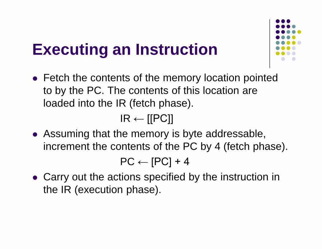
Executing an Instruction Fetch the contents of the memory location pointed
to by the PC. The contents of this location are loaded into the IR (fetch phase).
IR ← [[PC]] Assuming that the memory is byte addressable,
increment the contents of the PC by 4 (fetch phase).PC ← [PC] + 4
Carry out the actions specified by the instruction in the IR (execution phase).
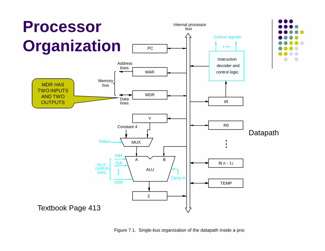
ProcessorOrganization
linesData
Addresslines
busMemory
Carry-in
ALU
PC
MAR
MDR
Y
Z
Add
XOR
Sub
bus
IR
TEMP
R0
controlALU
lines
Control signals
R n 1-
Instructiondecoder and
Internal processor
control logic
A B
Figure 7.1. Single-bus organization of the datapath inside a processor.
MUXSelect
Constant 4
Datapath
Textbook Page 413
MDR HAS TWO INPUTS
AND TWO OUTPUTS
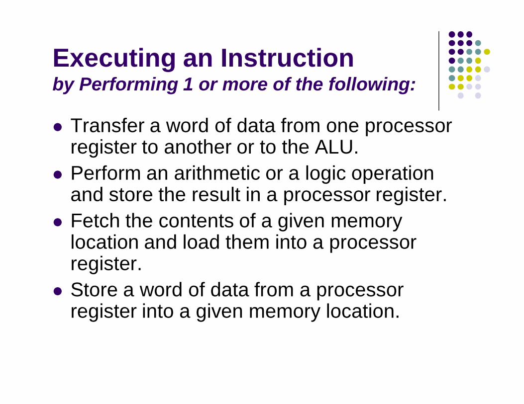
Executing an Instructionby Performing 1 or more of the following:
Transfer a word of data from one processor register to another or to the ALU.
Perform an arithmetic or a logic operation and store the result in a processor register.
Fetch the contents of a given memory location and load them into a processor register.
Store a word of data from a processor register into a given memory location.
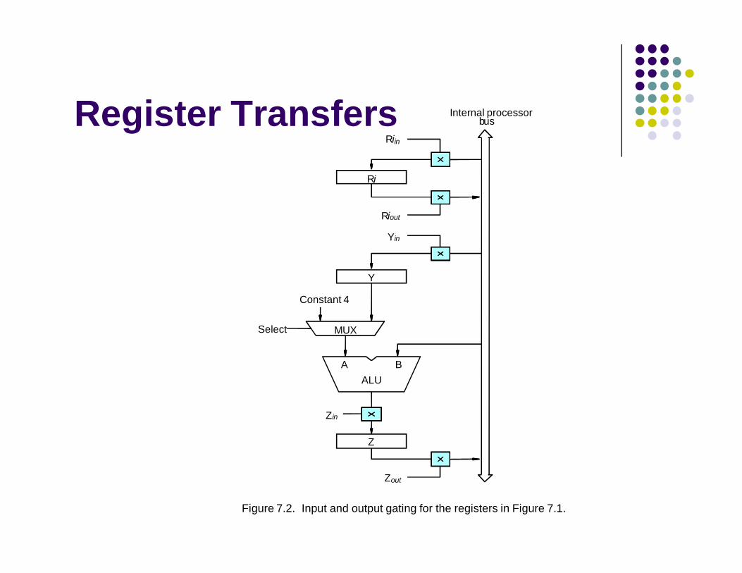
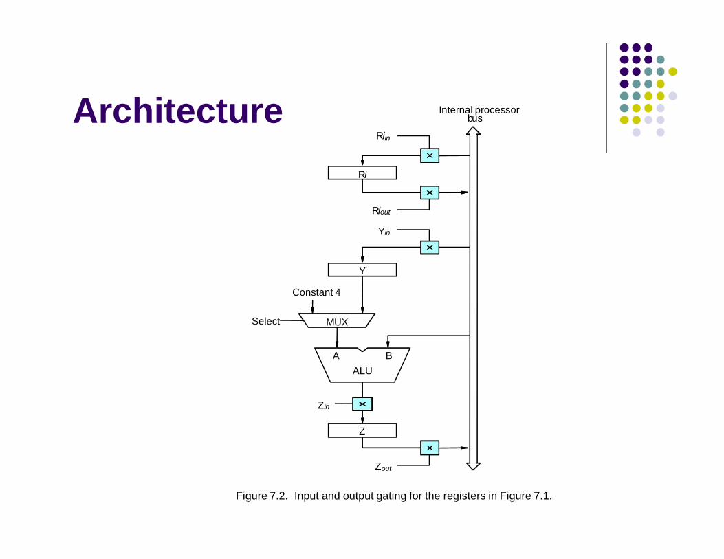
Register Transfers
BA
Z
ALU
Yin
Y
Zin
Zout
Riin
Ri
Riout
busInternal processor
Constant 4
MUX
Figure 7.2. Input and output gating for the registers in Figure 7.1.
Select
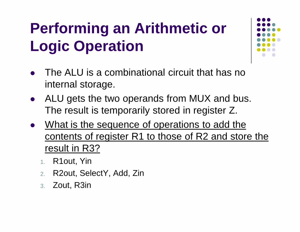
Performing an Arithmetic or Logic Operation The ALU is a combinational circuit that has no
internal storage. ALU gets the two operands from MUX and bus.
The result is temporarily stored in register Z. What is the sequence of operations to add the
contents of register R1 to those of R2 and store the result in R3?
1. R1out, Yin2. R2out, SelectY, Add, Zin3. Zout, R3in
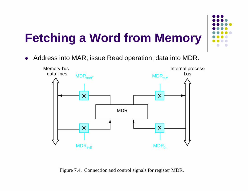
Fetching a Word from Memory Address into MAR; issue Read operation; data into MDR.
MDR
Memory-bus
Figure 7.4. Connection and control signals for register MDR.
data linesInternal processor
busMDRoutMDRoutE
MDRinMDRinE
Figure 7.4. Connection and control signals for register MDR.
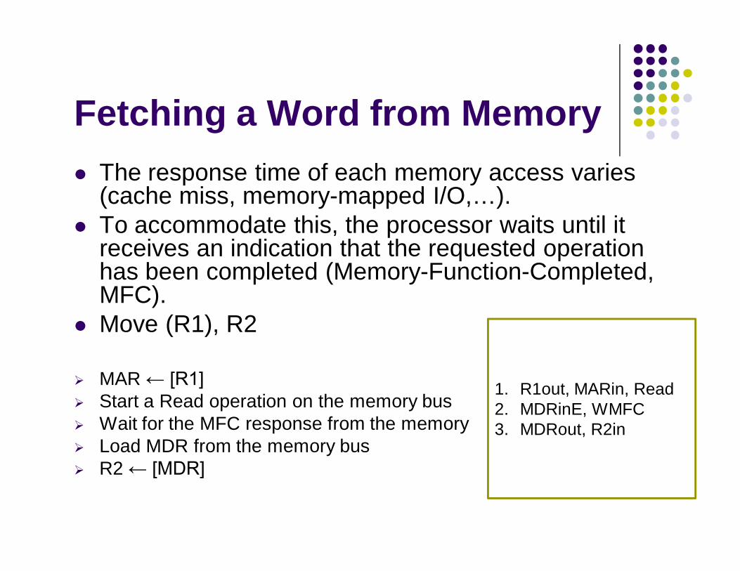
Fetching a Word from Memory The response time of each memory access varies
(cache miss, memory-mapped I/O,…). To accommodate this, the processor waits until it
receives an indication that the requested operation has been completed (Memory-Function-Completed, MFC).
Move (R1), R2
MAR ← [R1] Start a Read operation on the memory bus Wait for the MFC response from the memory Load MDR from the memory bus R2 ← [MDR]
1. R1out, MARin, Read2. MDRinE, WMFC3. MDRout, R2in
Execution of a Complete Instruction
Add (R3), R1 Fetch the instruction Fetch the first operand (the contents of the
memory location pointed to by R3) Perform the addition Load the result into R1
Architecture
BA
Z
ALU
Yin
Y
Zin
Zout
Riin
Ri
Riout
busInternal processor
Constant 4
MUX
Figure 7.2. Input and output gating for the registers in Figure 7.1.
Select
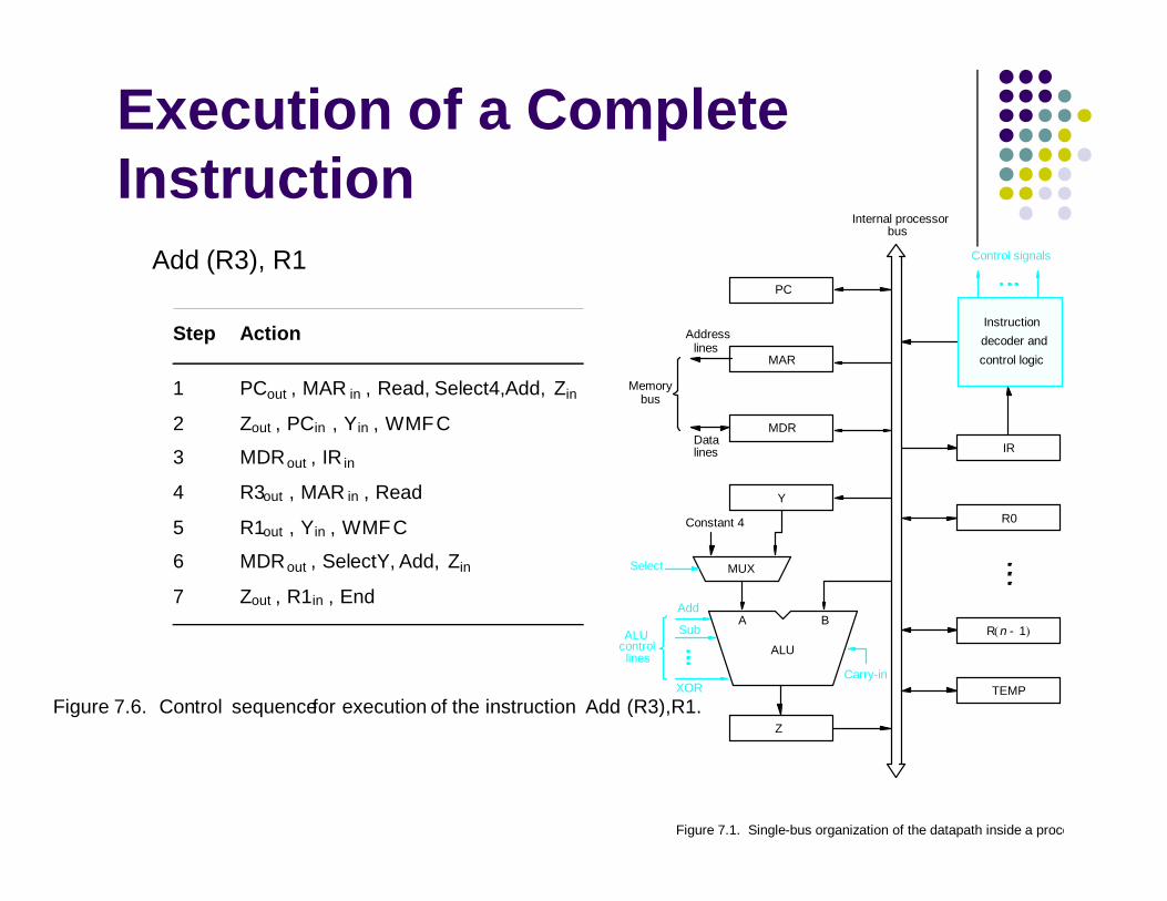
Execution of a Complete Instruction
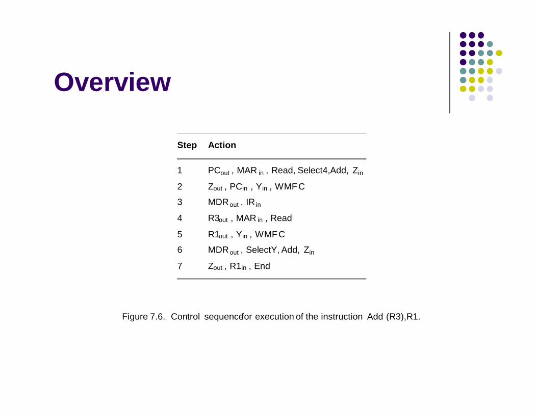
Step Action
1 PCout , MAR in , Read, Select4,Add, Zin
2 Zout , PCin , Yin , WMFC
3 MDRout , IR in
4 R3out , MAR in , Read
5 R1out , Yin , WMFC
6 MDRout , SelectY, Add, Zin
7 Zout , R1in , End
Figure 7.6. Control sequencefor execution of the instruction Add (R3),R1.
linesData
Addresslines
busMemory
Carry-in
ALU
PC
MAR
MDR
Y
Z
Add
XOR
Sub
bus
IR
TEMP
R0
controlALU
lines
Control signals
R n 1-
Instructiondecoder and
Internal processor
control logic
A B
Figure 7.1. Single-bus organization of the datapath inside a processor.
MUXSelect
Constant 4
Add (R3), R1
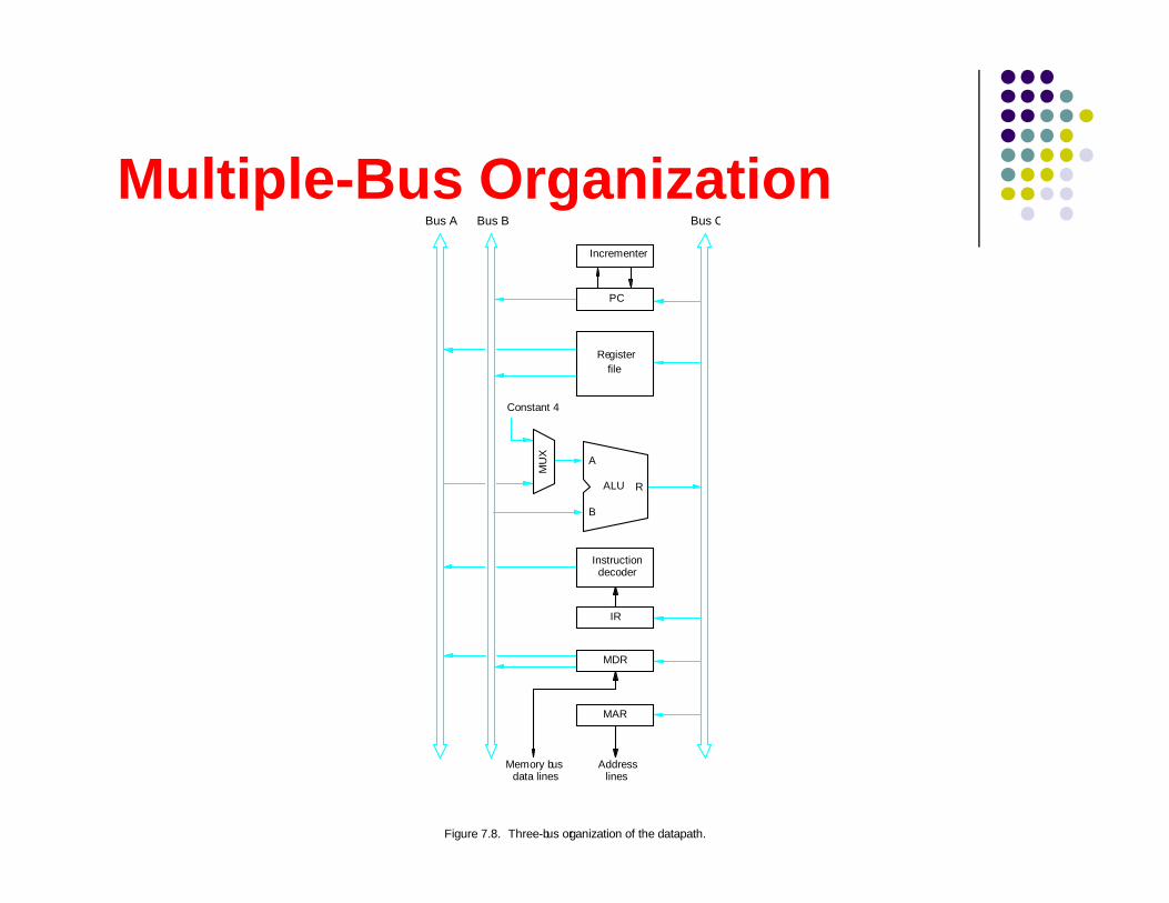
Multiple-Bus Organization
Memory busdata lines
Figure 7.8. Three-bus organization of the datapath.
Bus A Bus B Bus C
Instructiondecoder
PC
Registerfile
Constant 4
ALU
MDR
A
B
R
MU
X
Incrementer
Addresslines
MAR
IR
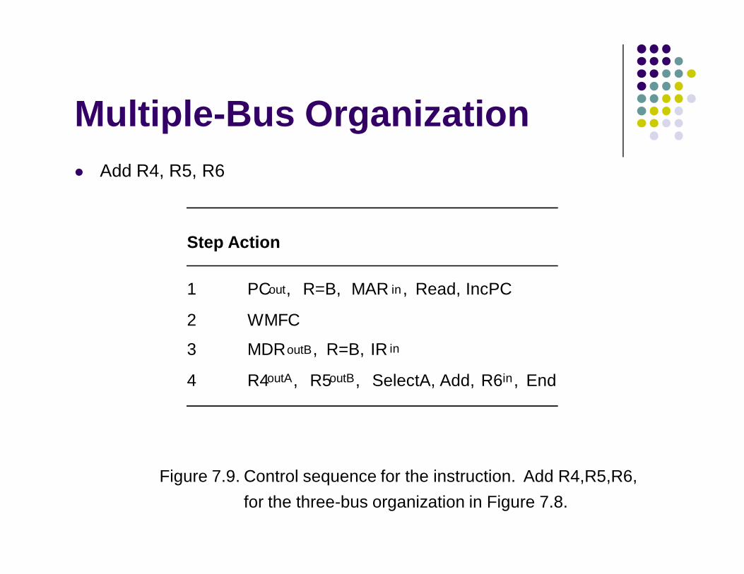
Multiple-Bus Organization Add R4, R5, R6
Step Action
1 PCout, R=B, MAR in , Read, IncPC
2 WMFC
3 MDRoutB, R=B, IR in
4 R4outA, R5outB, SelectA, Add, R6in, End
Figure 7.9. Control sequence for the instruction. Add R4,R5,R6,for the three-bus organization in Figure 7.8.

ASSIGNMENT What is the control
sequence for execution of the instruction
Add R1, R2including the instruction fetch phase? (Assume single bus architecture)
linesData
Addresslines
busMemory
Carry-in
ALU
PC
MAR
MDR
Y
Z
Add
XOR
Sub
bus
IR
TEMP
R0
controlALU
lines
Control signals
R n 1-
Instructiondecoder and
Internal processor
control logic
A B
Figure 7.1. Single-bus organization of the datapath inside a processor.
MUXSelect
Constant 4
Hardwired Control
Overview
To execute instructions, the processor must have some means of generating the control signals needed in the proper sequence.
Two categories: hardwired control and microprogrammed control
Hardwired system can operate at high speed; but with little flexibility.
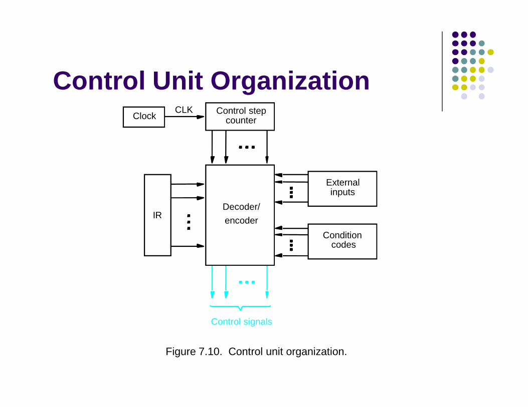
Control Unit Organization
Figure 7.10. Control unit organization.
CLKClock Control step
IR encoderDecoder/
Control signals
codes
counter
inputs
Condition
External
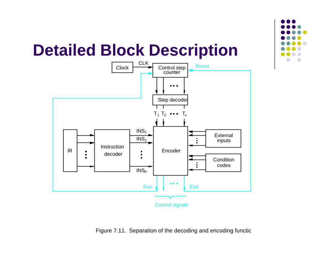
Detailed Block Description
Externalinputs
Figure 7.11. Separation of the decoding and encoding functions.
Encoder
ResetCLKClock
Control signals
counter
Run End
Conditioncodes
decoderInstruction
Step decoder
Control step
IR
T1 T2 Tn
INS1
INS2
INSm
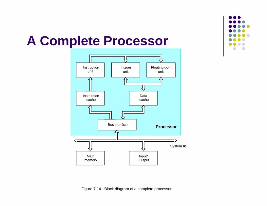
A Complete Processor
Instructionunit
Integerunit
Floating-pointunit
Instructioncache
Datacache
Bus interface
Mainmemory
Input/Output
System bus
Processor
Figure 7.14. Block diagram of a complete processor.
Microprogrammed Control
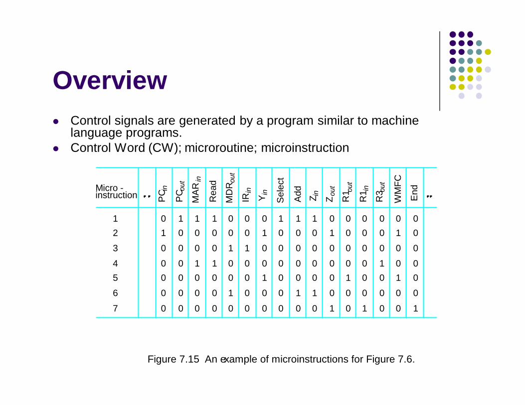
Overview Control signals are generated by a program similar to machine
language programs. Control Word (CW); microroutine; microinstruction
PC i
n
PC o
ut
MA
Rin
Rea
d
MD
R out
IRin
Y in
Sel
ect
Add Z in
Zou
t
R1 o
ut
R1 i
n
R3 o
ut
WM
FC
End
010000
0
000000
1
100000
0
100100
0
100100
0
001001
0
001000
0
010010
0
100000
0
100001
0
100001
0
010000
1
000010
0
000000
1
000100
0
010010
0
Micro -instruction
123456
7
Figure 7.15 An example of microinstructions for Figure 7.6.
Overview
Step Action
1 PCout , MAR in , Read, Select4,Add, Zin
2 Zout , PCin , Yin , WMFC
3 MDRout , IR in
4 R3out , MAR in , Read
5 R1out , Yin , WMFC
6 MDRout , SelectY, Add, Zin
7 Zout , R1in , End
Figure 7.6. Control sequencefor execution of the instruction Add (R3),R1.
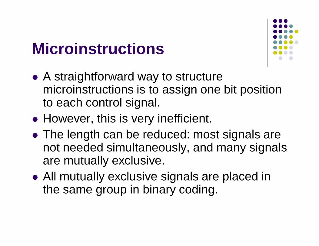
Microinstructions A straightforward way to structure
microinstructions is to assign one bit position to each control signal.
However, this is very inefficient. The length can be reduced: most signals are
not needed simultaneously, and many signals are mutually exclusive.
All mutually exclusive signals are placed in the same group in binary coding.
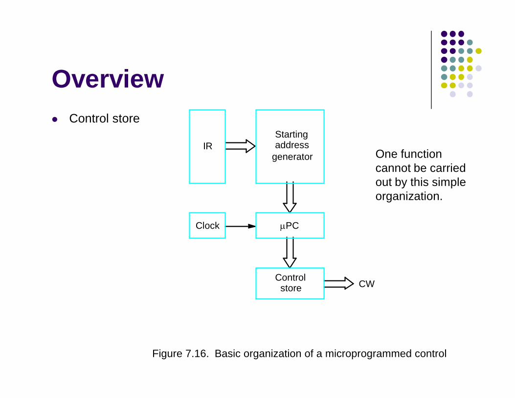
Overview Control store
Figure 7.16. Basic organization of a microprogrammed control unit.
storeControl
generator
Startingaddress
CW
Clock PC
IROne functioncannot be carriedout by this simpleorganization.
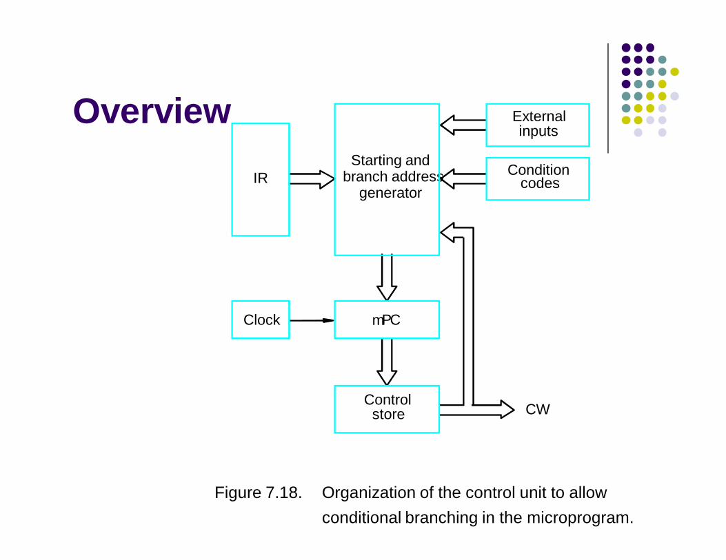
Overview
Figure 7.18. Organization of the control unit to allowconditional branching in the microprogram.
Controlstore
Clock
generator
Starting andbranch address Condition
codes
inputsExternal
CW
IR
mPC
THANK YOU
Reference:Computer Organization, Carl Hamacher, ZakyCh-7, Basic Processing Unit, P-411