Embed Size (px)
Citation preview

Band alignment at epitaxial BaSnO3/SrTiO3(001) and BaSnO3/LaAlO3(001)heterojunctionsScott A. Chambers, Tiffany C. Kaspar, Abhinav Prakash, Greg Haugstad, and Bharat Jalan Citation: Applied Physics Letters 108, 152104 (2016); doi: 10.1063/1.4946762 View online: http://dx.doi.org/10.1063/1.4946762 View Table of Contents: http://scitation.aip.org/content/aip/journal/apl/108/15?ver=pdfcov Published by the AIP Publishing Articles you may be interested in Photoconductivity of transparent perovskite semiconductor BaSnO3 and SrTiO3 epitaxial thin films Appl. Phys. Lett. 108, 092106 (2016); 10.1063/1.4943018 Enhanced electron mobility in epitaxial (Ba,La)SnO3 films on BaSnO3(001) substrates Appl. Phys. Lett. 108, 082105 (2016); 10.1063/1.4942509 BaSnO3 as a channel material in perovskite oxide heterostructures Appl. Phys. Lett. 108, 083501 (2016); 10.1063/1.4942366 La-doped BaSnO3—Degenerate perovskite transparent conducting oxide: Evidence from synchrotron x-rayspectroscopy Appl. Phys. Lett. 103, 042105 (2013); 10.1063/1.4816511 Origin of the superior conductivity of perovskite Ba(Sr)SnO3 Appl. Phys. Lett. 102, 112109 (2013); 10.1063/1.4798325
Reuse of AIP Publishing content is subject to the terms at: https://publishing.aip.org/authors/rights-and-permissions. Download to IP: 66.41.222.178 On: Thu, 14 Apr 2016
00:45:36
Band alignment at epitaxial BaSnO3/SrTiO3(001) and BaSnO3/LaAlO3(001)heterojunctions
Scott A. Chambers,1,a) Tiffany C. Kaspar,1 Abhinav Prakash,2 Greg Haugstad,3
and Bharat Jalan2,a)
1Physical and Computational Sciences Directorate, Pacific Northwest National Laboratory, Richland,Washington 99352, USA2Department of Chemical Engineering and Materials Science, University of Minnesota, Minneapolis,Minnesota 55455, USA3Characterization Facility, University of Minnesota, Minneapolis, Minnesota 55455, USA
(Received 29 January 2016; accepted 1 April 2016; published online 12 April 2016)
We have spectroscopically determined the optical bandgaps and band offsets at epitaxial interfaces
of BaSnO3 with SrTiO3(001) and LaAlO3(001). 28 u.c. BaSnO3 epitaxial films exhibit direct and
indirect bandgaps of 3.56 6 0.05 eV and 2.93 6 0.05 eV, respectively. The lack of a significant
Burstein-Moss shift corroborates the highly insulating, defect-free nature of the BaSnO3 films. The
conduction band minimum is lower in electron energy in 5 u.c. films of BaSnO3 than in SrTiO3 and
LaAlO3 by 0.4 6 0.2 eV and 3.7 6 0.2 eV, respectively. This result bodes well for the realization of
oxide-based, high-mobility, two-dimensional electron systems that can operate at ambient tempera-
ture, since electrons generated in the SrTiO3 by modulation doping, or at the BaSnO3/LaAlO3 inter-
face by polarization doping, can be transferred to and at least partially confined in the BaSnO3 film.
Published by AIP Publishing. [http://dx.doi.org/10.1063/1.4946762]
BaSnO3 (BSO) is an attractive wide-bandgap semicon-
ductor in the field of oxide electronics. When doped n-type,
BSO exhibits considerably higher room-temperature electron
mobility than SrTiO3 (STO), which has traditionally been
taken to be the leading perovskite oxide semiconductor.
Bulk single crystals of BSO have been shown to exhibit
room-temperature mobility values as high as 320 cm2/V s,1
whereas epitaxial films typically yield lower values thus far,
ranging between 10 and 150 cm2/V s.2–6 Additionally, BSO
has high optical transparency, rendering it of considerable in-
terest for transparent electronic technologies.7–10 While there
is potential to increase room-temperature electron mobility
in doped-BSO films through defect minimization, hetero-
structure engineering also provides a promising route to this
end. Heterostructure engineering provides pathways to iso-
late the carriers from scattering centers such as the dopants
from whence they come. This can be done by either modula-
tion doping (introducing dopants in a different material
across an interface from BSO) or polarization doping (induc-
ing charge transfer into non-polar BSO via electronic recon-
struction at the interface with a polar oxide). In either
scheme, the conduction band minimum in the BSO should
be of lower electron energy than that of the oxide to which
the BSO is joined in order to confine carriers in the BSO.
Under this condition, free carriers will readily spill over into
and remain in the BSO layer, provided the conduction band
offset is sufficiently large. Doped STO is a good choice as an
electron source for the modulation doping scheme, and
LaAlO3 (LAO) is suitable to test the polarization doping
approach.
To these ends, we have deposited epitaxial undoped
BSO films on undoped STO(001) and LAO(001) substrates
using hybrid molecular beam epitaxy (MBE) and have meas-
ured the band offsets and BSO band gap using ex situ x-ray
photoelectron spectroscopy (XPS) and spectroscopic ellips-
ometry (SE), respectively. Details of our hybrid MBE method
for BaSnO3 heteroepitaxy are discussed elsewhere.11,12 All
films were insulating, establishing that our growth process
does not unintentionally dope the BSO with O vacancies.
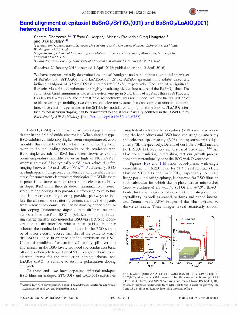
Figures 1(a) and 1(b) show out-of-plane, wide-angle
x-ray diffraction (XRD) scans for 28 6 1 unit cell (u.c.) BSO
films on STO(001) and LAO(001), respectively. A single
Bragg peak, indicating epitaxy, is observed for BSO films on
both substrates for which the in-plane lattice mismatches
(aBSO – asub)/aBSO) are þ5.1% (STO) and þ7.9% (LAO).
Finite thickness fringes are also evident, indicating excellent
crystallinity, as well as smooth surfaces and buried interfa-
ces. Contact mode AFM images of the film surfaces are
shown as insets. These images reveal atomically smooth
FIG. 1. Out-of-plane XRD scans for 28 u.c BSO on (a) STO(001) and (b)
LAO(001), along with AFM images of the film surfaces as insets. (c) RBS
(Heþþ at 4.3 MeV) and SIMNRA simulation for a 134 u.c BSO/STO(001)
specimen prepared under conditions identical to those used for growing the
5 and 28 u.c. films utilized to determine the band offsets.
a)Authors to whom correspondence should be addressed. Electronic addresses:
[email protected] and [email protected]
0003-6951/2016/108(15)/152104/4/$30.00 Published by AIP Publishing.108, 152104-1
APPLIED PHYSICS LETTERS 108, 152104 (2016)
Reuse of AIP Publishing content is subject to the terms at: https://publishing.aip.org/authors/rights-and-permissions. Download to IP: 66.41.222.178 On: Thu, 14 Apr 2016
00:45:36
surface morphology for both films, thereby corroborating the
XRD results. The c lattice parameters were determined to be
4.137(5) A and 4.122(5) A for films on STO and LAO, respec-
tively. These values are larger than the bulk value of 4.116 A,
which we attribute to incomplete strain relaxation in the
28 u.c. films. A much thicker (82 u.c.) film on LAO(001)
grown under the same conditions yielded lattice parameters
identical to those of bulk BSO, suggesting that the expanded clattice parameters in our 28 u.c. films are not due to cation
non-stoichiometry or oxygen vacancy defects, but rather to
incomplete strain relaxation.11 We show in Figure 1(c)
Rutherford backscattering spectrometry (RBS) data for a
134 u.c. BSO film on STO(001), along with a SIMNRA13 sim-
ulation yielding a Ba/Sn ratio of 0.996 6 0.010. The agree-
ment is very good, providing direct evidence for correct
stoichiometry in our BSO films.
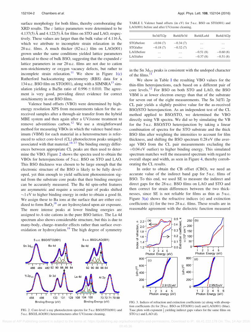
Valence band offsets (VBO) were determined by high-
energy resolution XPS from measurements taken for the as-
received samples after a through-air transfer from the hybrid
MBE system and then again after a UV/ozone treatment to
remove adventitious carbon.12 We use a straightforward
method for measuring VBOs in which the valence band max-
imum (VBM) for each material in a heterostructure is refer-
enced to select core-level (CL) photoelectron peaks uniquely
associated with that material.14–17 The binding energy differ-
ences between appropriate CL peaks are then used to deter-
mine the VBO. Figure 2 shows the spectra used to obtain the
VBOs for heterojunctions of 5 u.c. BSO on STO and LAO.
This BSO thickness was chosen to be large enough that the
electronic structure of the BSO is likely to be fully devel-
oped, yet thin enough to yield sufficient photoemission sig-
nal from the substrate core peaks that their binding energies
can be accurately measured. The Ba 4d spin-orbit features
are asymmetric and require a second pair of peaks shifted
�1 eV to higher binding energy in order to obtain a good fit.
We assign these to Ba ions at the surface that are either oxi-
dized to form BaO218 or are hydroxylated upon air exposure.
The more intense peaks at lower binding energies are
assigned to A-site cations in the pure BSO lattice. The La 4d
spectrum also shows considerable structure, but this is due to
many-body, charge–transfer effects rather than surface over-
oxidation or hydroxylation.19 The high degree of symmetry
in the Sn 3d5/2 peaks is consistent with the undoped character
of the films.11
We show in Table I the resulting VBO values for the
thin-film heterojunctions, each based on a different pair of
core levels.12 For BSO on both STO and LAO, the BSO
VBM is at lower electron energy than that of the substrate
for seven out of the eight measurements. The Sn 3d/Ti 2p
CL pair yields a slightly positive value for the as-received
BSO/STO heterojunction. As an independent test of the CL
method applied to BSO/STO, we determined the VBO
directly using VB spectra. We did so by simulating the VB
for the 5 u.c. BSO/STO heterojunction by taking a linear
combination of spectra for the STO substrate and the thick
BSO film after weighting the intensities to account for film
thickness, and shifting the BSO spectrum 0.28 eV (the aver-
age VBO from the CL pair measurements excluding the
þ0.04 eV outlier) to higher binding energy. This simulated
spectrum matches well the measured spectrum with regard to
overall shape and width, as seen in Figure 4, thereby corrob-
orating the CL results.
In order to obtain the CB offset (CBO), we need an
accurate value of the indirect band gap for 5 u.c. films of
BSO. To this end, we used SE to measure the indirect and
direct gaps for the 28 u.c. BSO films on LAO and STO and
then correct for strain differences between the two thick-
nesses, since SE is not reliable for films as thin as 5 u.c.
Figure 3(a) shows the refractive indices (n) and extinction
coefficients (k) for the two 28 u.c. films. These results are in
reasonable agreement with the dielectric function measured
FIG. 2. Core-level x-ray photoelectron spectra for 5 u.c BSO/STO(001) and
5 u.c. BSO/LAO(001) heterostructures after UV/ozone cleaning.
TABLE I. Valence band offsets (in eV) for 5 u.c. BSO on STO(001) and
LAO(001) before and after UV/ozone cleaning.
Sn3d/Ti2p Ba4d/Sr3d Ba4d/La4d Ba4d/Al2p
STO/before þ0.04 (7) �0.34 (7) … …
STO/after �0.18 (7) �0.32 (7) … …
LAO/before … … �0.51 (8) �0.60 (8)
LAO/after … … �0.37 (8) �0.51 (8)
FIG. 3. Indices of refraction and extinction coefficients (a) along with absorp-
tion coefficients (b) for 28 u.c. BSO on STO(001) (red) and LAO(001) (blue).
Tauc plots with exponent 12
yielding indirect gaps values for the same films on
STO (c) and LAO (d).
152104-2 Chambers et al. Appl. Phys. Lett. 108, 152104 (2016)
Reuse of AIP Publishing content is subject to the terms at: https://publishing.aip.org/authors/rights-and-permissions. Download to IP: 66.41.222.178 On: Thu, 14 Apr 2016
00:45:36
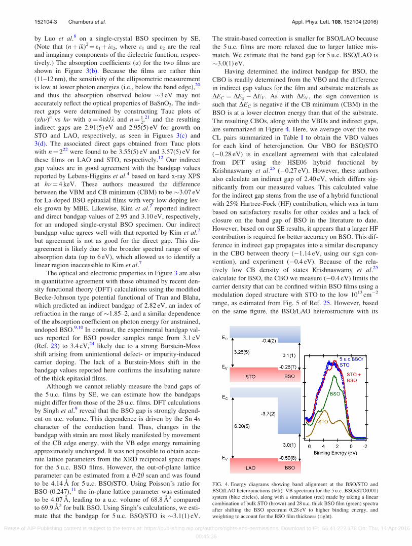
by Luo et al.8 on a single-crystal BSO specimen by SE.
(Note that (nþ ik)2¼ e1þ ie2, where e1 and e2 are the real
and imaginary components of the dielectric function, respec-
tively.) The absorption coefficients (a) for the two films are
shown in Figure 3(b). Because the films are rather thin
(11–12 nm), the sensitivity of the ellipsometric measurement
is low at lower photon energies (i.e., below the band edge),20
and thus the absorption observed below �3 eV may not
accurately reflect the optical properties of BaSnO3. The indi-
rect gaps were determined by constructing Tauc plots of
(ah�)n vs h� with a¼ 4pk/k and n¼ 12,21 and the resulting
indirect gaps are 2.91(5) eV and 2.95(5) eV for growth on
STO and LAO, respectively, as seen in Figures 3(c) and
3(d). The associated direct gaps obtained from Tauc plots
with n¼ 222 were found to be 3.55(5) eV and 3.57(5) eV for
these films on LAO and STO, respectively.12 Our indirect
gap values are in good agreement with the bandgap values
reported by Lebens-Higgins et al.4 based on hard x-ray XPS
at h�¼ 4 keV. These authors measured the difference
between the VBM and CB minimum (CBM) to be �3.07 eV
for La-doped BSO epitaxial films with very low doping lev-
els grown by MBE. Likewise, Kim et al.7 reported indirect
and direct bandgap values of 2.95 and 3.10 eV, respectively,
for an undoped single-crystal BSO specimen. Our indirect
bandgap value agrees well with that reported by Kim et al.7
but agreement is not as good for the direct gap. This dis-
agreement is likely due to the broader spectral range of our
absorption data (up to 6 eV), which allowed us to identify a
linear region inaccessible to Kim et al.7
The optical and electronic properties in Figure 3 are also
in quantitative agreement with those obtained by recent den-
sity functional theory (DFT) calculations using the modified
Becke-Johnson type potential functional of Tran and Blaha,
which predicted an indirect bandgap of 2.82 eV, an index of
refraction in the range of �1.85–2, and a similar dependence
of the absorption coefficient on photon energy for unstrained,
undoped BSO.9,10 In contrast, the experimental bandgap val-
ues reported for BSO powder samples range from 3.1 eV
(Ref. 23) to 3.4 eV,24 likely due to a strong Burstein-Moss
shift arising from unintentional defect- or impurity-induced
carrier doping. The lack of a Burstein-Moss shift in the
bandgap values reported here confirms the insulating nature
of the thick epitaxial films.
Although we cannot reliably measure the band gaps of
the 5 u.c. films by SE, we can estimate how the bandgaps
might differ from those of the 28 u.c. films. DFT calculations
by Singh et al.9 reveal that the BSO gap is strongly depend-
ent on u.c. volume. This dependence is driven by the Sn 4scharacter of the conduction band. Thus, changes in the
bandgap with strain are most likely manifested by movement
of the CB edge energy, with the VB edge energy remaining
approximately unchanged. It was not possible to obtain accu-
rate lattice parameters from the XRD reciprocal space maps
for the 5 u.c. BSO films. However, the out-of-plane lattice
parameter can be estimated from a h-2h scan and was found
to be 4.14 A for 5 u.c. BSO/STO. Using Poisson’s ratio for
BSO (0.247),11 the in-plane lattice parameter was estimated
to be 4.07 A, leading to a u.c. volume of 68.8 A3 compared
to 69.9 A3 for bulk BSO. Using Singh’s calculations, we esti-
mate that the bandgap for 5 u.c. BSO/STO is �3.1(1) eV.
The strain-based correction is smaller for BSO/LAO because
the 5 u.c. films are more relaxed due to larger lattice mis-
match. We estimate that the band gap for 5 u.c. BSO/LAO is
�3.0(1) eV.
Having determined the indirect bandgap for BSO, the
CBO is readily determined from the VBO and the difference
in indirect gap values for the film and substrate materials as
DEC ¼ DEg � DEV . As with DEV , the sign convention is
such that DEC is negative if the CB minimum (CBM) in the
BSO is at a lower electron energy than that of the substrate.
The resulting CBOs, along with the VBOs and indirect gaps,
are summarized in Figure 4. Here, we average over the two
CL pairs summarized in Table I to obtain the VBO values
for each kind of heterojunction. Our VBO for BSO/STO
(�0.28 eV) is in excellent agreement with that calculated
from DFT using the HSE06 hybrid functional by
Krishnaswamy et al.25 (�0.27 eV). However, these authors
also calculate an indirect gap of 2.40 eV, which differs sig-
nificantly from our measured values. This calculated value
for the indirect gap stems from the use of a hybrid functional
with 25% Hartree-Fock (HF) contribution, which was in turn
based on satisfactory results for other oxides and a lack of
closure on the band gap of BSO in the literature to date.
However, based on our SE results, it appears that a larger HF
contribution is required for better accuracy on BSO. This dif-
ference in indirect gap propagates into a similar discrepancy
in the CBO between theory (�1.14 eV, using our sign con-
vention), and experiment (�0.4 eV). Because of the rela-
tively low CB density of states Krishnaswamy et al.25
calculate for BSO, the CBO we measure (�0.4 eV) limits the
carrier density that can be confined within BSO films using a
modulation doped structure with STO to the low 1013 cm�2
range, as estimated from Fig. 5 of Ref. 25. However, based
on the same figure, the BSO/LAO heterostructure with its
FIG. 4. Energy diagrams showing band alignment at the BSO/STO and
BSO/LAO heterojunctions (left). VB spectrum for the 5 u.c. BSO/STO(001)
system (blue circles), along with a simulation (red) made by taking a linear
combination of bulk STO (brown) and 28 u.c. thick BSO film (green) spectra
after shifting the BSO spectrum 0.28 eV to higher binding energy, and
weighting to account for the BSO film thickness (right).
152104-3 Chambers et al. Appl. Phys. Lett. 108, 152104 (2016)
Reuse of AIP Publishing content is subject to the terms at: https://publishing.aip.org/authors/rights-and-permissions. Download to IP: 66.41.222.178 On: Thu, 14 Apr 2016
00:45:36
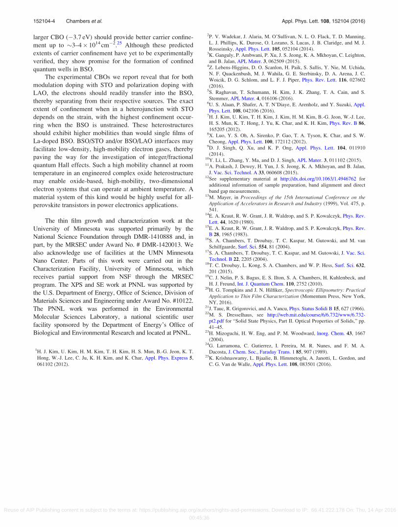
larger CBO (�3.7 eV) should provide better carrier confine-
ment up to �3–4� 1014 cm�2.25 Although these predicted
extents of carrier confinement have yet to be experimentally
verified, they show promise for the formation of confined
quantum wells in BSO.
The experimental CBOs we report reveal that for both
modulation doping with STO and polarization doping with
LAO, the electrons should readily transfer into the BSO,
thereby separating from their respective sources. The exact
extent of confinement when in a heterojunction with STO
depends on the strain, with the highest confinement occur-
ring when the BSO is unstrained. These heterostructures
should exhibit higher mobilities than would single films of
La-doped BSO. BSO/STO and/or BSO/LAO interfaces may
facilitate low-density, high-mobility electron gases, thereby
paving the way for the investigation of integer/fractional
quantum Hall effects. Such a high mobility channel at room
temperature in an engineered complex oxide heterostructure
may enable oxide-based, high-mobility, two-dimensional
electron systems that can operate at ambient temperature. A
material system of this kind would be highly useful for all-
perovskite transistors in power electronics applications.
The thin film growth and characterization work at the
University of Minnesota was supported primarily by the
National Science Foundation through DMR-1410888 and, in
part, by the MRSEC under Award No. # DMR-1420013. We
also acknowledge use of facilities at the UMN Minnesota
Nano Center. Parts of this work were carried out in the
Characterization Facility, University of Minnesota, which
receives partial support from NSF through the MRSEC
program. The XPS and SE work at PNNL was supported by
the U.S. Department of Energy, Office of Science, Division of
Materials Sciences and Engineering under Award No. #10122.
The PNNL work was performed in the Environmental
Molecular Sciences Laboratory, a national scientific user
facility sponsored by the Department of Energy’s Office of
Biological and Environmental Research and located at PNNL.
1H. J. Kim, U. Kim, H. M. Kim, T. H. Kim, H. S. Mun, B.-G. Jeon, K. T.
Hong, W.-J. Lee, C. Ju, K. H. Kim, and K. Char, Appl. Phys. Express 5,
061102 (2012).
2P. V. Wadekar, J. Alaria, M. O’Sullivan, N. L. O. Flack, T. D. Manning,
L. J. Phillips, K. Durose, O. Lozano, S. Lucas, J. B. Claridge, and M. J.
Rosseinsky, Appl. Phys. Lett. 105, 052104 (2014).3K. Ganguly, P. Ambwani, P. Xu, J. S. Jeong, K. A. Mkhoyan, C. Leighton,
and B. Jalan, APL Mater. 3, 062509 (2015).4Z. Lebens-Higgins, D. O. Scanlon, H. Paik, S. Sallis, Y. Nie, M. Uchida,
N. F. Quackenbush, M. J. Wahila, G. E. Sterbinsky, D. A. Arena, J. C.
Woicik, D. G. Schlom, and L. F. J. Piper, Phys. Rev. Lett. 116, 027602
(2016).5S. Raghavan, T. Schumann, H. Kim, J. K. Zhang, T. A. Cain, and S.
Stemmer, APL Mater. 4, 016106 (2016).6U. S. Alaan, P. Shafer, A. T. N’Diaye, E. Arenholz, and Y. Suzuki, Appl.
Phys. Lett. 108, 042106 (2016).7H. J. Kim, U. Kim, T. H. Kim, J. Kim, H. M. Kim, B.-G. Jeon, W.-J. Lee,
H. S. Mun, K. T. Hong, J. Yu, K. Char, and K. H. Kim, Phys. Rev. B 86,
165205 (2012).8X. Luo, Y. S. Oh, A. Sirenko, P. Gao, T. A. Tyson, K. Char, and S. W.
Cheong, Appl. Phys. Lett. 100, 172112 (2012).9D. J. Singh, Q. Xu, and K. P. Ong, Appl. Phys. Lett. 104, 011910
(2014).10Y. Li, L. Zhang, Y. Ma, and D. J. Singh, APL Mater. 3, 011102 (2015).11A. Prakash, J. Dewey, H. Yun, J. S. Jeong, K. A. Mkhoyan, and B. Jalan,
J. Vac. Sci. Technol. A 33, 060608 (2015).12See supplementary material at http://dx.doi.org/10.1063/1.4946762 for
additional information of sample preparation, band alignment and direct
band gap measurements.13M. Mayer, in Proceedings of the 15th International Conference on the
Application of Accelerators in Research and Industry (1999), Vol. 475, p.
541.14E. A. Kraut, R. W. Grant, J. R. Waldrop, and S. P. Kowalczyk, Phys. Rev.
Lett. 44, 1620 (1980).15E. A. Kraut, R. W. Grant, J. R. Waldrop, and S. P. Kowalczyk, Phys. Rev.
B 28, 1965 (1983).16S. A. Chambers, T. Droubay, T. C. Kaspar, M. Gutowski, and M. van
Schilfgaarde, Surf. Sci. 554, 81 (2004).17S. A. Chambers, T. Droubay, T. C. Kaspar, and M. Gutowski, J. Vac. Sci.
Technol. B 22, 2205 (2004).18T. C. Droubay, L. Kong, S. A. Chambers, and W. P. Hess, Surf. Sci. 632,
201 (2015).19C. J. Nelin, P. S. Bagus, E. S. Ilton, S. A. Chambers, H. Kuhlenbeck, and
H. J. Freund, Int. J. Quantum Chem. 110, 2752 (2010).20H. G. Tompkins and J. N. Hilfiker, Spectroscopic Ellipsometry: Practical
Application to Thin Film Characterization (Momentum Press, New York,
NY, 2016).21J. Tauc, R. Grigorovici, and A. Vancu, Phys. Status Solidi B 15, 627 (1966).22M. S. Dresselhaus, see http://web.mit.edu/course/6/6.732/www/6.732-
pt2.pdf for “Solid State Physics, Part II. Optical Properties of Solids,” pp.
41–45.23H. Mizoguchi, H. W. Eng, and P. M. Woodward, lnorg. Chem. 43, 1667
(2004).24G. Larramona, C. Gutierrez, I. Pereira, M. R. Nunes, and F. M. A.
Dacosta, J. Chem. Soc., Faraday Trans. 1 85, 907 (1989).25K. Krishnaswamy, L. Bjaalie, B. Himmetoglu, A. Janotti, L. Gordon, and
C. G. Van de Walle, Appl. Phys. Lett. 108, 083501 (2016).
152104-4 Chambers et al. Appl. Phys. Lett. 108, 152104 (2016)
Reuse of AIP Publishing content is subject to the terms at: https://publishing.aip.org/authors/rights-and-permissions. Download to IP: 66.41.222.178 On: Thu, 14 Apr 2016
00:45:36