Embed Size (px)
Citation preview

Switchable Induced Polarization in LaAlO3/SrTiO3 HeterostructuresC. W. Bark,† P. Sharma,‡ Y. Wang,‡ S. H. Baek,† S. Lee,† S. Ryu,† C. M. Folkman,† T. R. Paudel,‡
A. Kumar,∥ S. V. Kalinin,∥ A. Sokolov,‡ E. Y. Tsymbal,‡ M. S. Rzchowski,§ A. Gruverman,‡
and C. B. Eom*,†
†Department of Materials Science and Engineering, University of Wisconsin, Madison, Wisconsin 53706, United States‡Department of Physics and Astronomy, Nebraska Center for Materials and Nanoscience, University of Nebraska, Lincoln, Nebraska68588, United States§Department of Physics, University of Wisconsin, Madison, Wisconsin 53706, United States∥Center for Nanophase Materials Sciences, Oak Ridge National Laboratory, Oak Ridge, Tennessee 37831, United States
*S Supporting Information
ABSTRACT: Demonstration of a tunable conductivity of theLaAlO3/SrTiO3 interfaces drew significant attention to thedevelopment of oxide electronic structures where electronicconfinement can be reduced to the nanometer range. Whilethe mechanisms for the conductivity modulation are quitedifferent and include metal−insulator phase transition andsurface charge writing, generally it is implied that this effect is aresult of electrical modification of the LaAlO3 surface (eitherdue to electrochemical dissociation of surface adsorbates orfree charge deposition) leading to the change in the two-dimensional electron gas (2DEG) density at the LaAlO3/SrTiO3 (LAO/STO) interface. In this paper, using piezoresponse forcemicroscopy we demonstrate a switchable electromechanical response of the LAO overlayer, which we attribute to the motion ofoxygen vacancies through the LAO layer thickness. These electrically induced reversible changes in bulk stoichiometry of theLAO layer are a signature of a possible additional mechanism for nanoscale oxide 2DEG control on LAO/STO interfaces.
KEYWORDS: Heterointerfaces, complex oxides, oxygen vacancies, piezoresponse force microscopy
Since the discovery of a conducting two-dimensionalelectron gas (2DEG) at the interface between the
insulating oxide materials LaAlO3 (LAO) and SrTiO3(STO),1 significant advances in altering and controlling itsproperties are positioning oxide 2DEG-based heterostructuresas viable electronic devices. These control mechanisms includefield effect from a back or front gate,2,3 epitaxial strain,4 atomicsubstitution at the 2DEG,5 and local heterostructuremodification with scanning probe microscopy (SPM) techni-ques.6−10 In comparison to other methods, SPM has proved tobe extremely flexible, allowing nanoscale rewritable modulationand control of the 2DEG conductivity.An important aspect of the scanning probe modification of
the 2DEG is a deposition of electric charge on the LaAlO3
surface, and its subsequent electrostatic modulation of the2DEG carrier concentration. In its most basic form, thecapacitor structure formed by the LAO dielectric causespositive LAO surface charge to induce negative charge at theopposing capacitor plate formed by the 2DEG, therebyenhancing the 2DEG conductance. Electrostatic force micros-copy (EFM) measurements indicate that a probing tippositively biased with respect to the 2DEG deposits positivecharge on the LAO surface, and negatively biased tip depositsnegative LAO surface charge.10 This process has been shown to
be consistent with a varying density of surface OH− and H+
ions controlled by the probing tip.11
In this Letter, using a combination of piezoresponse forcemicroscopy (PFM)12 and electrostatic force microscopy(EFM)13 we demonstrate a new mechanism of SPM-inducedcontrol of the 2DEG in LAO/STO heterostructures related to aswitchable electromechanical behavior of the LAO layer. ThePFM response we have detected in LAO is very similar to thatobserved in ferroelectric materials. Its most likely origin,however, is a spatial polarization induced in the LAO layer dueto redistribution of oxygen vacancies. The symmetry ofundistorted LAO precludes any intrinsic small-signal switchableelectromechanical response as the noncentrosymmetric struc-tural distortions in the LAO layer of LAO/STO hetero-structures are not switchable. On the other hand, there isgrowing evidence14,15 that the electric fields generated innanoscale systems by even modest electric potentials aresufficiently large to modify materials by injecting or rearrangingdefect structures, particularly those related to oxygen.16,17 Toexplain the results of our PFM studies of LAO/STO
Received: September 6, 2011Revised: February 28, 2012Published: March 8, 2012
Letter
pubs.acs.org/NanoLett
© 2012 American Chemical Society 1765 dx.doi.org/10.1021/nl3001088 | Nano Lett. 2012, 12, 1765−1771
heterostructures, we propose that under an applied bias theoxygen vacancy structure distribution throughout the LAOthickness is reversibly modified, leading to the switchableelectromechanical response, and to a corresponding change in2DEG carrier concentration.Epitaxial LaAlO3/SrTiO3 thin film heterostructures were
grown on various single crystal substrates using pulsed-laserdeposition (PLD) with in situ high-pressure reflection high-energy electron diffraction (RHEED). Here we focus on twosets of samples, one in which the LAO thickness was varied,and the other set with varying biaxial strain set by the substrate.The first set of samples had an epitaxial top LaAlO3 layers of
various thickness in the range from 5 to 80 unit cells (u.c.),grown on 50 u.c. thick (001) STO films on (001) (LaAlO3)0.3−(Sr2AlTaO3)0.7 (LSAT) substrates. In addition, to performcomparative analysis epitaxial LAO films were grown onconducting oxide Sr0.2Ca0.8RuO3 (SCRO) thin films on LSATsubstrates.The second set of samples had varying degrees of biaxial
tensile strain in the LAO layer obtained by growingLAO(20uc)/STO(50uc) heterostructures on LSAT (2.1%LAO strain), and (110) DyScO3 (DSO) (4.1% LAO strain)substrates. In addition, LAO was grown directly on Ti-terminated single crystal STO (3.0% LAO strain). Details ofthe growth process and structural information can be found inref 6. In all heterostructures, the LAO, STO, and SCRO layersurfaces were atomically smooth with single unit cell high stepswith all layers fully coherent with the LSAT substrate. In-situRHEED growth indicated layer-by-layer growth, similar toLaAlO3 films on SrTiO3 single crystal substrates.Our basic results are indicated in Figure 1, where combined
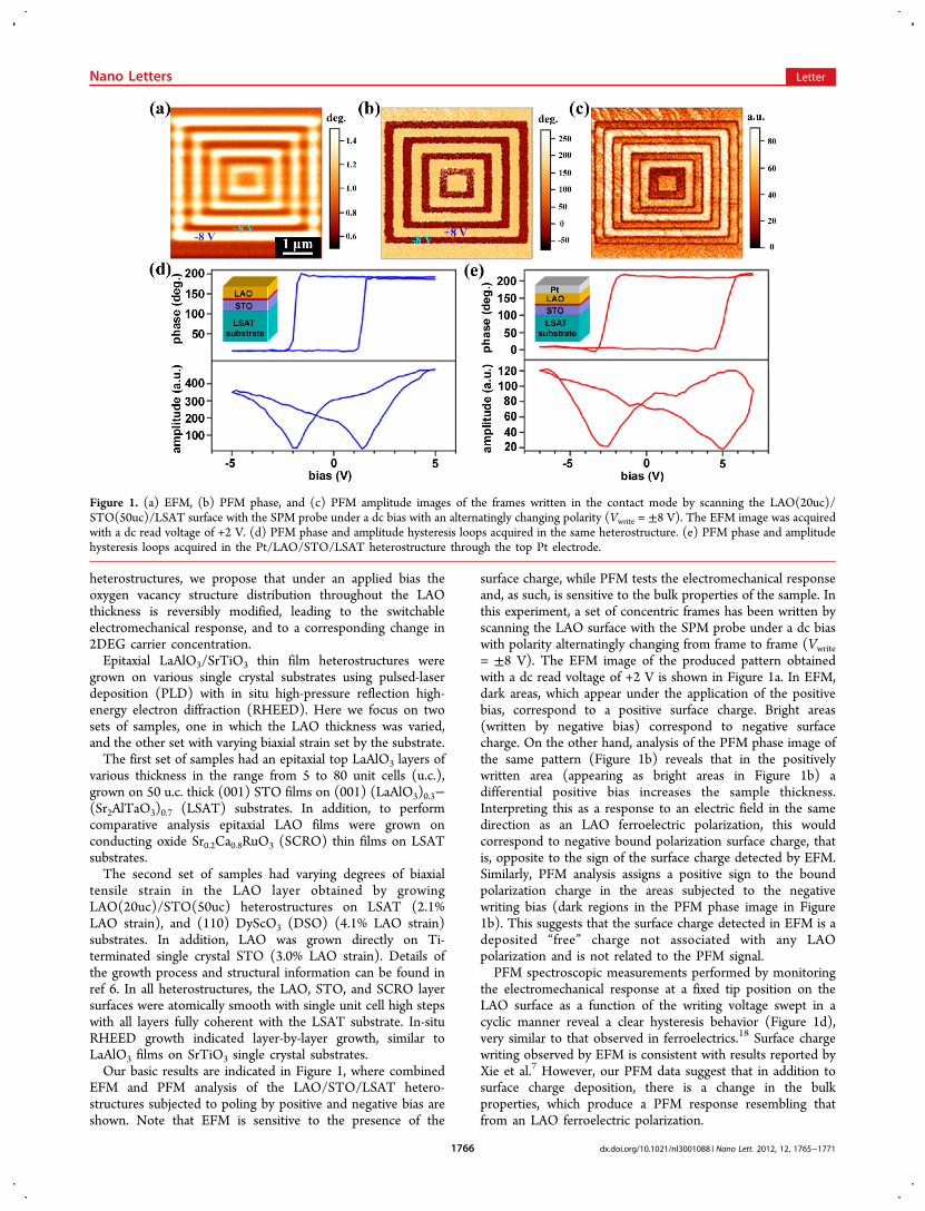
EFM and PFM analysis of the LAO/STO/LSAT hetero-structures subjected to poling by positive and negative bias areshown. Note that EFM is sensitive to the presence of the
surface charge, while PFM tests the electromechanical responseand, as such, is sensitive to the bulk properties of the sample. Inthis experiment, a set of concentric frames has been written byscanning the LAO surface with the SPM probe under a dc biaswith polarity alternatingly changing from frame to frame (Vwrite= ±8 V). The EFM image of the produced pattern obtainedwith a dc read voltage of +2 V is shown in Figure 1a. In EFM,dark areas, which appear under the application of the positivebias, correspond to a positive surface charge. Bright areas(written by negative bias) correspond to negative surfacecharge. On the other hand, analysis of the PFM phase image ofthe same pattern (Figure 1b) reveals that in the positivelywritten area (appearing as bright areas in Figure 1b) adifferential positive bias increases the sample thickness.Interpreting this as a response to an electric field in the samedirection as an LAO ferroelectric polarization, this wouldcorrespond to negative bound polarization surface charge, thatis, opposite to the sign of the surface charge detected by EFM.Similarly, PFM analysis assigns a positive sign to the boundpolarization charge in the areas subjected to the negativewriting bias (dark regions in the PFM phase image in Figure1b). This suggests that the surface charge detected in EFM is adeposited “free” charge not associated with any LAOpolarization and is not related to the PFM signal.PFM spectroscopic measurements performed by monitoring
the electromechanical response at a fixed tip position on theLAO surface as a function of the writing voltage swept in acyclic manner reveal a clear hysteresis behavior (Figure 1d),very similar to that observed in ferroelectrics.18 Surface chargewriting observed by EFM is consistent with results reported byXie et al.7 However, our PFM data suggest that in addition tosurface charge deposition, there is a change in the bulkproperties, which produce a PFM response resembling thatfrom an LAO ferroelectric polarization.
Figure 1. (a) EFM, (b) PFM phase, and (c) PFM amplitude images of the frames written in the contact mode by scanning the LAO(20uc)/STO(50uc)/LSAT surface with the SPM probe under a dc bias with an alternatingly changing polarity (Vwrite = ±8 V). The EFM image was acquiredwith a dc read voltage of +2 V. (d) PFM phase and amplitude hysteresis loops acquired in the same heterostructure. (e) PFM phase and amplitudehysteresis loops acquired in the Pt/LAO/STO/LSAT heterostructure through the top Pt electrode.
Nano Letters Letter
dx.doi.org/10.1021/nl3001088 | Nano Lett. 2012, 12, 1765−17711766

In PFM imaging of ultrathin oxide heterostructures, there isalways a concern that an electromechanical signal could beaffected by electrostatic tip−sample interaction effects.However, in our measurements the PFM signal arises mainlyfrom the true electromechanical response and not from theelectrostatic effect. Evidence for this includes a stronglynonlinear bias-dependent behavior of the PFM amplitudesignal, PFM phase change range of almost 180°, as well as anessentially different appearance of the PFM amplitude andphase images with much sharper features than in the EFMimage. This conclusion is further supported by the fact thatboth EFM and PFM images of the written patterns exhibitquite different relaxation rates (EFM signal decaying muchslower than the PFM signal, i.e., 2−3 h for EFM and tens ofminutes for PFM). Most importantly, we have also observed aswitchable electromechanical response and hysteresis behaviorin the LAO/STO/LSAT samples with top Pt electrodes(Figure 1e). In this geometry, electrostatic forces are typicallytoo small to affect the PFM signal19−21 and the contribution ofpurely electrostatic interactions to the PFM hysteresis behaviorcan be largely excluded.The next question we addressed was the source of the
switchable PFM behavior: does it stem from the STO or LAOlayer, or is it a result of the interplay between responses from
both layers and an interaction with the 2DEG? To answer thisquestion we grew a 20 u.c. thick LAO layer on top of thelattice-matched conducting oxide Sr0.2Ca0.8RuO3 (SCRO), onan LSAT substrate (Figure 2a). Remarkably, poling andsubsequent PFM imaging as well as PFM spectroscopicmeasurements revealed pattern maps and hysteresis behavior(Figure 2b,c) closely resembling the corresponding dataobtained on LAO/STO/LSAT heterostructure (Figure 1c,d).For an LAO substrate with no conducting bottom electrode, wefind (by EFM measurements) that surface charge is depositedunder electrical bias, but no PFM response is observed. For a50 u.c. thick STO layer deposited on the SrRuO3/SrTiO3substrate, only EFM and no PFM contrast has been recorded(Figure 2d−f). We conclude, therefore, that the switchableelectromechanical response in LAO/STO stems from the LAOlayer with the conducting bottom interface playing a role.Switchable piezoresponse and hysteretic PFM behavior
makes it very tempting to interpret the observed features as amanifestation of a spontaneous electric polarization directlyswitchable with external electric field. However, attributing theswitchable electromechanical response to a switchable polar-ization seems to be in contradiction with the known polarbehavior of LAO/STO heterostructures. In undistorted LAO,positively charged (LaO)+ atomic layers and negatively charged
Figure 2. (a) Schematic diagram of the LAO/SCRO/LSAT heterostructure, (b) a corresponding PFM amplitude image of the written pattern, and(c) PFM hysteresis loops acquired in the LAO/SCRO/LSAT heterostructure. (d) Schematic diagram of the STO/SRO/STO heterostructure, (e)corresponding PFM amplitude, and (f) EFM images acquired in the STO/SRO/STO heterostructure after poling (poled regions are marked bysquare dashed-line blocks).
Nano Letters Letter
dx.doi.org/10.1021/nl3001088 | Nano Lett. 2012, 12, 1765−17711767

(AlO2)− atomic layers create an average electric polarization
throughout the layer. A true ferroelectric state in LAO,however, generally competes with and is suppressed byoctahedral rotations. It is predicted to appear at compressivestrains of more than −3% if rotations are not allowed.22 Recentexperimental work23,24 indicates that an epitaxial interface witha non-antiferrodistortive material will suppress octahedralrotations near the interface. It has been predicted theoreticallythat free-standing biaxially strained SrTiO3 under electricalshort-circuit boundary conditions can develop a [001] (out-of-plane) polarization.25,26 Experimental TEM27,28 and synchro-tron radiation X-ray scattering studies29,30 show that addition ofan LAO overlayer to strained STO results in ferroelectric-likestructural distortions in the SrTiO3 layer leading to furtherenhancement of polarization throughout its thickness. How-ever, any electric polarization in either LAO or in STO layers isnot expected to be switchable as they are structurally frozen.To clarify the physical origin of the switchable electro-
mechanical response in LAO/STO heterostructures weinvestigated the thickness dependence of the hysteresis loopparameters as well as the effect of substrate-induced strain onthe PFM signal stability. The thickness dependence of the PFMbehavior has been studied using LAO films of various thickness(in the range from 5 to 80 u.c.) grown on STO(50uc)/LSATsubstrates (Figure 3a). All heterostructures, except for that withthe LAO thickness of 5 u.c. exhibited a switchable electro-mechanical response characterized by hysteretic behavior(Figure 3b). From the hysteresis loops analysis, it can beseen that the initial (before poling) piezoresponse amplitudesignal decreases with thickness (Figure 3c), consistent withincreased electric field spreading in the LAO layers with largerthickness. In addition, the nucleation bias Vn (determined asthe bias voltage of the PFM amplitude minimum) exhibits anincrease with LAO layer thickness before saturating at largethickness. The fact that nucleation bias is thickness dependentand PFM response is nonlinear on thickness in principle isconsistent with the field-induced ionic migration process orferroelectric polarization switching. However, in conjunctionwith the observed decay of the written domain patterns, thisdata suggests that the presence of stable ferroelectric polar-ization as a dominant mechanism can be excluded.Further information related to the mechanism of the
electromechanical response has been obtained by studyingthe relaxation behavior of the written states of a LAO(20uc)/STO(50uc)/LSAT heterostructure. Square-shaped patternshave been written on the LAO surface using a dc writingvoltage Vwrite = ±6 V. PFM images were obtained at various
time intervals with the decrease in PFM amplitude signal beingan indicator of the relaxation behavior. Figure 4 shows a timedependence of the PFM amplitude signal in a region poled with−6 V (corresponds to unstable state). The PFM amplitude P(t)is consistent with a logarithmic law decay PR(t) = P0 − α ln(t/t0), where P0 is the initial PFM amplitude, α is the decayconstant, and t0 a characteristic time. The PFM response inregions poled with +6 V showed no time decay.We have found that the relaxation rate of the PFM amplitude
signal depends on LAO lattice strain. The inset to Figure 4shows composite PFM amplitude images with the left partsshowing maps taken immediately after poling and right partsacquired at a later time. It can be seen that larger tensile strainleads to a significant increase in the relaxation rate: LAO with2% tensile strain on a STO/LSAT template shows a retentiontime of the order of 104 s in comparison with only 102 s in theLAO/STO/DSO with 4% tensile strain.Hysteresis in the PFM response can be considered in terms
of hysteretic switching of an electric polarization in the LAOlayer. As ferroelectricity is not a plausible mechanism, wepropose an alternative mechanism that could produce aswitchable PFM response that is related to oxygen vacancymigration under the influence of an applied electric field.Indeed, the molar volume of materials generally increases withoxygen vacancies (since cation effective radii in lower oxidationstates are higher), so that injection and removal of oxygen
Figure 3. (a) Schematic diagram of the LAO/STO/LSAT heterostructure. Thickness of LaAlO3 layer was varied from 5 to 80 unit cells. (b) PFMphase and amplitude hysteresis loops of the LAO/STO/LSAT heterostructures for various LAO thicknesses. (c) Thickness dependence of thenucleation bias Vn and zero-bias piezoresponse signal PRS.
Figure 4. Relaxation behavior of the LAO(20uc)/STO(50uc)heterostructures. Insets show composite PFM amplitude images ofthe LAO layers on the different substrates imposing various degrees oftensile strain. Left parts of the composite images illustrate patternsimmediately after poling and right parts show patterns at a later time.A solid line represents a logarithmic function PR(t) = P0 − α ln(t/t0).
Nano Letters Letter
dx.doi.org/10.1021/nl3001088 | Nano Lett. 2012, 12, 1765−17711768

vacancies can cause the strain modulation leading to switchableelectromechanical response. More fundamentally, a switchableinternal electric field or induced electric polarization would biasthe intrinsic electrostriction and produce a switchable PFMresponse. The required electric field could arise from a bistablesurface charge or a bistable distribution of oxygen vacancies,driven by the tip bias. Recent theoretical calculations31 showthat oxygen vacancies have a small local energy minimum at theLaO−TiO2 interface. The LAO surface is also expected to be alocal energy minimum for oxygen vacancies, which provides amechanism for two stable oxygen vacancy configurations at theLAO surface and the LAO−STO interface. Note thatpreviously demonstrated surface charge deposition that control2DEG conductivity2 would not be present in our samples withPt top electrodes.The electrically induced oxygen vacancy migration mecha-
nism is consistent with our measurements of PFM relaxation inLAO/STO heterostructures on substrates with different latticeconstants (Figure 4). Biaxial tensile strain leads to a unit cellvolume increase, which likely leads to an increase in the densityof oxygen vacancies. The higher oxygen vacancy concentrationwould lead to faster diffusivity, and faster relaxation of the PFMsignal, consistent with the experimental results described above.The above considerations are supported by a simple model
for oxygen vacancy formation based on the electrostatic energyof the system. The model assumes that a uniform electric fieldis developed in the polar LAO layer and in STO due to thefree-electron charge distributed within confinement width λnear the interface.32 Oxygen vacancies are formed within aplane located at distance d away from the interface. Twouncompensated electrons move to the interface leavingpositively charged holes at the vacancy site.31,33 The hole−electron pair creates an electric field. If oxygen vacancies arecreated in LAO this electric field is opposite to the intrinsicfield in the LAO and thus the energy is reduced. The reductionin the electrostatic energy increases when moving to the LAOsurface. This creates a minimum for the oxygen vacancyformation energy at the LAO surface (Figure 5). If oxygenvacancies are created in STO the field due to electron−hole
pairs partly compensates the electric field due the free-electroncharge penetrating into STO which reduces the electrostaticenergy. However, this reduction is limited to the confinementwidth λ because at larger distances oxygen vacancies create anuncompensated electric field, which enhances the electrostaticenergy (Figure 5). Thus, the model predicts the existence oftwo minima in the oxygen formation energy that may beresponsible for the hysteretic behavior observed in ourexperiment.It is also possible that oxygen vacancies are not concentrated
at the LAO surface or at the LAO/STO interface but aredistributed nonuniformly throughout the LAO thickness. Inthis case, an electric polarization could be induced by theresulting strain gradient through the flexoelectric effect.34 Thispolarization would be switchable by an electric field along withthe oxygen vacancy strain gradient and would bias theelectrostriction in the same way as an electric field arisingfrom external sources.These mechanisms produce a PFM response consistent with
our observations. Recent experimental and theoretical study35
has demonstrated a large electrostrictive response of the LAOlayer in LAO/STO heterostructures, finding an electric-fielddependent c-axis strain of ε = −(0.2 Å2/V2)E2, with E theelectric field in the LAO layer. Here E is made up of aswitchable static field and the ac field from the PFM tip. Takinga switchable field on the order of half the 0.24 V/Å intrinsicLAO electric field arising from interlayer charge transfer givesan ac strain of ε ≈ −(0.4 Å2/V2) EdcEac ≈ −(20 pm/V)Eac. Therelative phase between the PFM response and Eac would thenshift by 180° when Edc is reversed, which is consistent with theexperimental data. Such a switchable electric field in principlecould also arise from hysteretic behavior of electric chargedeposited on the bare LAO surface by the PFM tip. However,as was mentioned above, the effect of the surface charge can beruled out based on the fact that the switchable PFM response ispresent even in the LAO/STO heterostructures with the Pt topelectrode (Figure 1e) when the electrostatic contribution to themeasured response is negligibly small.Finally, as the strained LAO layers on the Ti-terminated
(001) STO exhibit not only a switchable polarization but alsotwo-dimensional electron gas (2DEG),6,36 and it has beenpredicted that polarization can be used to control 2DEGproperties at oxide heterointerfaces,37,38 we have investigatedcorrelations between these two effects. Specifically, we havefound that the conductivity of the 2DEG can be modulatedsignificantly via LAO poling. A 40 × 20 μm2 LAO/STO bridgestructure has been fabricated on the LSAT substrate by ionmilling to make it suitable for 4-point probe transport and PFMmeasurements (Figure 6a). The 20 × 20 μm2 area across thebridge has been poled first by +9 V and then by −9 V by a PFMtip as is schematically shown in Figure 6a. Resulting change inthe interface resistance upon poling by almost a factor of 2 isillustrated in Figure 6b. Note the apparent bias dependence ofresistance for the −9 V poled state, which is actually resistancerelaxation during the measurement cycle consistent withrelaxation of the piezoresponse signal shown in Figure 4.To summarize, we have observed switchable, hysteretic PFM
response from the LAO layer in the LAO/STO/LSAT andLAO/SCRO/LSAT heterostructures. We propose that oxygenvacancies mobile under the influence of an applied electric fieldhave a bistable configuration and that this is responsible forswitchable hysteretic PFM response and contributes toswitchable 2DEG conductance in LAO/STO heterostructures.
Figure 5. Oxygen vacancy formation energy calculated using theelectrostatic model. Parameters used in the calculation are as follows:the free electron density at the interface σ = 0.1 e/u.c., the electrondensity due to oxygen vacancies σu = 0.5 e/u.c. (red line) and σu = 0.25e/u.c. (blue line), and the dielectric constant of LAO εL = 24 and thatof STO εS =36.
Nano Letters Letter
dx.doi.org/10.1021/nl3001088 | Nano Lett. 2012, 12, 1765−17711769

This represents an additional control mechanism for mod-ification of the electrical properties of heterointerfaces. Theproposed mechanism of switchable electromechanical responseshould be active in many other oxide heterosystems, but itsdetailed manifestation likely depends on a number of subtleties,such as oxygen octahedra rotations and distortions, strain, andlattice couplings at the nanoscale. Control of this phenomenonwill enable new structures and devices that exploit nanoscaleelectromechanical coupling. A more complete understanding ofthe proposed mechanism is necessary to provide this control,which would be facilitated by advances in the nanoscalemeasurement of vacancy concentrations and their dynamics.39
■ ASSOCIATED CONTENT*S Supporting InformationThis section provides detailed information on materials andmethods used to fabricate and characterize devices the LAO/STO heterostructures. This material is available free of chargevia the Internet at http://pubs.acs.org.
■ AUTHOR INFORMATIONCorresponding Author*E-mail: [email protected].
NotesThe authors declare no competing financial interest.
■ ACKNOWLEDGMENTSThe work at University of Wisconsin was supported by theNational Science Foundation (NSF) under Grant DMR-0906443. The work at University of Nebraska was supportedby the Materials Research Science and Engineering Center(NSF Grant DMR-0820521), by the U.S. Department ofEnergy, Office of Basic Energy Sciences, Division of MaterialsSciences and Engineering (DOE Grant DE-SC0004876),Cross-Disciplinary Semiconductor Research Program of Semi-conductor Research Corporation (SRC Grant G11016),Experimental Program to Stimulate Competitive Research(NSF Grant EPS-1010674), and the Nebraska ResearchInitiative.
■ REFERENCES(1) Ohtomo, A.; Hwang, H. Y. Nature 2004, 427, 423−426.(2) Caviglia, A. D.; Gariglio, S.; Reyren, N.; Jaccard, D.; Schneider,T.; Gabay, M.; Thiel, S.; Hammerl, G.; Mannhart, J.; Triscone, J.-M.Nature 2008, 456, 624−627.(3) Bell, C.; Harashima, S.; Kozuka, Y.; Kim, M.; Kim, B. G.; Hikita,Y.; Hwang, H. Y. Phys. Rev. Lett. 2009, 103, 226802.(4) Bark, C. W.; Felker, D. A.; Wang, Y.; Zhang, Y.; Jang, H. W.;Folkman, C. M.; Park, J. W.; Baek, S. H.; Zhou, H.; Fong, D. D.; Pan,X. Q.; Tsymbal, E. Y.; Rzchowski, M. S.; Eom, C. B. Proc. Natl. Acad.Sci. U.S.A. 2011, 108, 4720−4724.(5) Jang, H. W.; Felker, D. A.; Bark, C. W.; Wang, Y.; Niranjan, M.K.; Nelson, C. T.; Zhang, Y.; Su, D.; Folkman, C. M.; Baek, S. H.; Lee,S.; Janicka, K.; Zhu, Y.; Pan, X. Q.; Fong, D. D.; Tsymbal, E. Y.;Rzchowski, M. S.; Eom, C. B. Science 2011, 331, 886−889.(6) Cen, C.; Thiel, S.; Mannhart, J.; Levy, J. Science 2009, 323, 1026−1030.(7) Xie, Y.; Bell, C.; Yajima, T.; Hikita, Y.; Hwang, H. Y. Nano Lett.2010, 10, 2588−2591.(8) Cen, C.; Thiel, S.; Hammerl, G.; Schneider, C. W.; Andersen, K.E.; Hellberg, C. S.; Mannhart, J.; Levy, J. Nat. Mater. 2008, 7, 298−302.(9) Park, J. W.; Bogorin, D. F.; Cen, C.; Felker, D. A.; Zhang, Y.;Nelson, C. T.; Bark, C. W.; Folkman, C. M.; Pan, X. Q.; Rzchowski, M.S.; Levy, J.; Eom, C. B. Nat. Commun. 2010, 1, 94.(10) Xie, Y.; Bell, C.; Hikita, Y.; Hwang, H. Y. Adv. Mater. 2011, 23,1744−1747.(11) Bi, F.; Bogorin, D. F.; Cen, C.; Bark, C. W.; Park, J.-W.; Eom,C.-B.; Levy, J. Appl. Phys. Lett. 2010, 97, 173110.(12) Gruverman, A.; Auciello, O.; Tokumoto, H. Annu. Rev. Mater.Sci. 1998, 28, 101−123.(13) Gruverman, A.; Kholkin, A. Rep. Prog. Phys. 2006, 69, 2443−2474.(14) Zafar, S.; Jagannathan, H.; Edge, L. F.; Gupta, D. Appl. Phys.Lett. 2011, 98, 152903.(15) Ueno, K.; Shimotani, H.; Iwasa, Y.; Kawasaki, M. Appl. Phys.Lett. 2010, 96, 252107.(16) Gramm, A.; Zahner, T.; Spreitzer, U.; Rossler, R.; Pedarnig, J.D.; Bauerle, D.; Lengfellner, H. Europhys. Lett. 2000, 49, 501−506.(17) Nian, Y. B.; Strozier, J.; Wu, N. J.; Chen, X.; Ignatiev, A. Phys.Rev. Lett. 2007, 98, 146403.(18) Gruverman, A.; Kalinin, S. V. J. Mater. Sci. 2006, 41, 107−116.
Figure 6. Tuning resistivity of 2DEG via poling in the LAO(20uc)/STO(50uc)/LSAT heterostructure. (a) An upper panel shows an optical imageof the structure fabricated on the LSAT substrate for 2DEG resistivity measurements. A lower panel shows a schematic view of the part of thestructure marked by a yellow block on the upper panel. A dashed-line block indicates the area that has been poled by a biased probe. (b) Biasdependence of the interface resistance after poling by Vwrite = −9 V and Vwrite = +9 V. Note the 2DEG resistance change during measurements for the−9 V poled state is in agreement with the relaxation behavior illustrated in Figure 4. The inset schematically shows the changes in 2DEG uponpoling.
Nano Letters Letter
dx.doi.org/10.1021/nl3001088 | Nano Lett. 2012, 12, 1765−17711770

(19) Kalinin, S. V.; Karapetian, E.; Kachanov, M. Phys. Rev. B 2004,70, 184101.(20) Kalinin, S. V.; Bonnell, D. A. Phys. Rev. B 2002, 65, 125408.(21) Rodriguez, B. J.; Jesse, S.; Habelitz, S.; Proksch, R.; Kalinin, S. V.Nanotechnology 2009, 20, 195701.(22) Hatt, A. J.; Spaldin, N. A. Phys. Rev. B 2010, 82, 195402.(23) Borisevich, A. Y.; Chang, H. J.; Huijben, M.; Oxley, M. P.;Okamoto, S.; Niranjan, M. K.; Burton, J. D.; Tsymbal, E. Y.; Chu, Y.H.; Yu, P.; Ramesh, R.; Kalinin, S. V.; Pennycook, S. J. Phys. Rev. Lett.2010, 105, 087204.(24) May, S. J.; Kim, J.-W.; Rondinelli, J. M.; Karapetrova, E.;Spaldin, N. A.; Bhattacharya, A.; Ryan, P. J. Phys. Rev. B 2010, 82,014110.(25) Antons, A.; Neaton, J. B.; Rabe, K. M.; Vanderbilt, D. Phys. Rev.B 2005, 71, 024102.(26) Sheng, G.; Li, Y. L.; Zhang, J. X.; Choudhury, S.; Jia, Q. X.;Gopalan, V.; Schlom, D. G.; Liu, Z. K.; Chen, L. Q. Appl. Phys. Lett.2010, 96, 232902.(27) Maurice, J.-L.; Carretero, C.; Casanove, M.-J.; Bouzehouane, K.;Guyard, S.; Larquet, E.; Contour, J.-P. Physica Status Solidi A 2006,203, 2209−2214.(28) Jia, C. L.; Mi, S. B.; Faley, M.; Poppe, U.; Schubert, J.; Urban, K.Phys. Rev. B 2009, 79, 081405.(29) Vonk, V.; Huijben, M.; Driessen, K. J. I.; Tinnemans, P.;Brinkman, A.; Harkema, S.; Graafsma, H. Phys. Rev. B 2007, 75,235417.(30) Willmott, P. R.; Pauli, S. A.; Herger, R.; Schleputz, C. M.;Martoccia, D.; Patterson, B. D.; Delley, B.; Clarke, R.; Kumah, D.;Cionca, C.; Yacoby, Y. Phys. Rev. Lett. 2007, 99, 155502.(31) Zhong, Z.; Xu, P. X.; Kelly, P. J. Phys. Rev. B 2010, 82, 165127.(32) Janicka, K.; Velev, J. P.; Tsymbal, E. Y. Phys. Rev. Lett. 2009, 102,106803.(33) Bristowe, N.; Littlewood, P.; Artacho, E. Phys. Rev. B 2011, 83,205405.(34) Nguyen, T. L.; Dokiya, M.; Wang, S.; Tagawa, H.; Hashimoto,T. Solid State Ionics. 2000, 130, 229−241.(35) Cancellieri, C.; Fontaine, D.; Gariglio, S.; Reyren, N.; Caviglia,A. D.; Fete, A.; Leake, S. J.; Pauli, S. A.; Willmott, P. R.; Stengel, M.;Ghosez, P.; Triscone, J.-M. Phys. Rev. Lett. 2011, 107, 056102.(36) Nakagawa, N.; Hwang, H. Y.; Muller, D. A. Nat. Mater. 2006, 5,204−209.(37) Niranjan, M. K.; Wang, Y.; Jaswal, S. S.; Tsymbal, E. Y. Phys.Rev. Lett. 2009, 103, 016804.(38) Wang, Y.; Niranjan, M. K.; Jaswal, S. S.; Tsymbal, E. Y. Phys.Rev. B 2009, 80, 165130.(39) Bryant, B.; Renner, C.; Tokunaga, Y.; Tokura, Y.; Aeppli, G. NatCommun. 2011, 2, 212.
Nano Letters Letter
dx.doi.org/10.1021/nl3001088 | Nano Lett. 2012, 12, 1765−17711771


![Study of Frequency and Polarization Reconfigurable on ... · antenna for switchable polarization [9] is proposed by corner truncated square radiating patch and independent biased](https://img.pdfslide.us/doc/110x75/5ea39adb82bfea49295100d9/study-of-frequency-and-polarization-reconfigurable-on-antenna-for-switchable.jpg)


![University of Groningen Engineering complex oxide ... · of polarization-controlled charge transport [37, 27] and switchable photovoltaic ef-fects. [28, 29] The latter behavior was](https://img.pdfslide.us/doc/110x75/5f91fc13228f336da15c25f7/university-of-groningen-engineering-complex-oxide-of-polarization-controlled.jpg)