Embed Size (px)
Citation preview

Backend Flow OptimizationBackend Flow Optimization Using Design Structure MatrixUsing Design Structure Matrix
Badari Kommandur Prithvi Bannerjee
System Project Management –Fall 2003
1
Courtesy of Badari Kommandur and Prithvi Bannerjee. Used with permission.
OverviewOverview• Introduction • Motivation for backend flow optimization • CPU Design Phases • Silicon Debug Process Flow • Design Structure Matrix Application to
Backend Process • Managing Unplanned Iterations • Key Learnings • Recommendations
System Project Management –Fall 2003
2

P(X-1)P (X)
Use test vehicles,synchronize
P(X-2)
~ 107 ~ 108
Use test vehicles,synchronize
~ 107 ~ 108
Intel Deve
System Project Management –Fall 2003
MotivationMotivation
• Design philosophy aims atreducing risk with time
• Significant source ofuncertainty – Market Needs – Technology (Design &
Manufacturing) – Resource roll offs
• Capital commitmentneeds to be made before uncertainty resolves
• Backup options hard topursue in parallel
Research Development Manufacturing
$/year:
Risk taking:
Take high risks
Reduce risks rapidly
Keeprisks low
~ 109
Innovation Speed Volume
Research Development Manufacturing
P(X-1)P (X)
$/year:
Risktaking:
Takehigh risks
Reducerisks rapidly
Keeprisks low
Takehigh risks
Reducerisks rapidly
Keeprisks low
Use test vehicles,synchronize
P(X-2)
~ 109
~ 107 ~ 108 ~ 109
Innovation Speed Volume
lopment PhilosophyIntel Development PhilosophyIntel Development Philosophy
Significant capital has to be committed based on demand forecasts and technology investment needs to made well before uncertainty has resolved.
Modeling and prototypes not sufficient to model real designs sufficiently.
Objective is to reduce risks as design moves into development and manufacturing rapidly. At any time instant, at least 3 generations of CPU designs are in different stages of execution. (i.e There may be 3 designs each for IA-32, IA-64 and mobile platforms). These teams are geographically distributed and may be located in US (multiple sites), Malaysia, India, Israel. A given design may be developed concurrently across sites.
3

MotivationMotivation
• Backend flow optimization is critical for revenue growth – Reduce TT$ – Performance Enhancement – Yield Improvement – Reduce Lead time for
Demand (MCT Reduction) • Intel does not use formal
methods for IPT formation – Use of DSM to validate
current composition of IPT • Analyze process to reduce time
spent in backend flow
Revenue Shortfall (Million $)
$-
$500
$1,000
$1,500
$2,000
$2,500
0% 2% 4% 6% 8% 10% 12%
% Yield Loss R
even
u e S
h o r
t f a l
l
Revenue Shortfall (Million $)
System Project Management –Fall 2003
– Reduce iterations? 1% Yield Loss can cost $100 Million/Quarter1% Yield Loss can cost $100 Million/Quarter
Assuming a annual microprocessor shipment rate of 100 million units, ASP (Average selling price) of $200, Yield Impact to revenue is calculated.Added opportunity cost and capacity to meet demand can result in total impact to be ~2X
Tapeout to PTQ (Production tape quality) Î First time units can be sold to customers for revenue
4

MethodologyMethodology• Interviews with technical and management leads in
Pentium 4tm design team (Design, Manufacturing, Planning, QRE)
• Integration of a priori knowledge about backend flow – Hands on experience on previous generations of
CPU designs • Review of methodology/process documentation for
Product Development Teams
• Analysis of functional effort spent on last 4 generation of IA-32 processors (Lead designs and Compaction designs)
• Design Structure Analysis of Backend Flow System Project Management –Fall 2003
5

CPU Design PhasesCPU Design Phases
Lead Architecture
Definition
Roadmap Decision Planning
Front End Development
Technology Readiness
Product Implementation
Plan
Design Execution Mask Generation Wafer Procesiing
Sort Testing Assembly & Packaging Class Testing Test, Verification
and Validation
Launch
Failure Analysis/ Quality and Reliability
Engineering
System Project Management –Fall 2003
Front end devlopment involves the integration of University research, Marketing, OEM, Lead Users, Finance, HR, Executive Staff, Strategic Planning, Platform Solutions Group, Test Technology and Manufacturing groups in defining the lead architecture.
Product roadmap planning involves continuous input from the competitive intelligence group, OEMs and strategic planning group. These can result frequently in roadmap changes to react to market environment and competitive position. (Pentium 4TM HT Extreme Edition launch before OpteronTM launch)
Product Implementation Plan results in generation of External Product Specification (released to customers) and Internal Product Specification based on which design execution starts.
Backend development involves tight integration of all functional teams through Integrated Product Teams, War Rooms and Taskforce meetings. Typically takes 3-4 quarters from tapeout of lead architecture to HVM. Quality and Reliability engineering works closely with design teams and PDT to certify design for launch while meeting DPM goals.
6

System Project Management –Fall 2003
CPU Design Effort TrendsCPU Design Effort TrendsThroughput Time in Weeks
0
50
100
150
200
250
300
Project Name
TPT
in W
eeks
Tech Readiness Front End Development Execution Si Debug/Ramp
Si Debug/Ramp 62.52 41.28 51.72 42 52.08
Execution 77.88 37.56 55.08 97.08 78.12
Front End Development 46.92 38.88 0 62.28 62.4
Tech Readiness 78 15.6 0 46.8 78.12
Lead A Compaction A Lead B Lead C Lead D
Lead Design ~ 4-5 Yrs
Compaction ~ 2 yrs
There are two types of microprocessor projects at Intel. Lead Architecture Projects and Compaction. Lead Architecture involve radical innovations in design, process and manufacturing. Initial manufacturing is on N-1 process generation for short duration of time before migration to lead process technology. These are used to validate design concepts and process technology.
Compaction involve minor modifications to architecture and major focus is on incremental innovations to improve performance, yield and reduce cost for high volume manufacturing. These are manufactured on the latest generation of process technology.
Average throughput time for a lead architecture is about 4-5 years and constant effort is ongoing to reduce it. The CPU development effort can be broken into four main phases. •Technology Readiness •Front End Development •Execution •Backend (Silicon Debug/Ramp)
Lead B does not show first two phases but still is called Lead Design due to significant architectural and design changes incorporated based on product roadmap changes.
Lead Design takes approximately twice the design effort as a compaction project.
7
System Project Management –Fall 2003
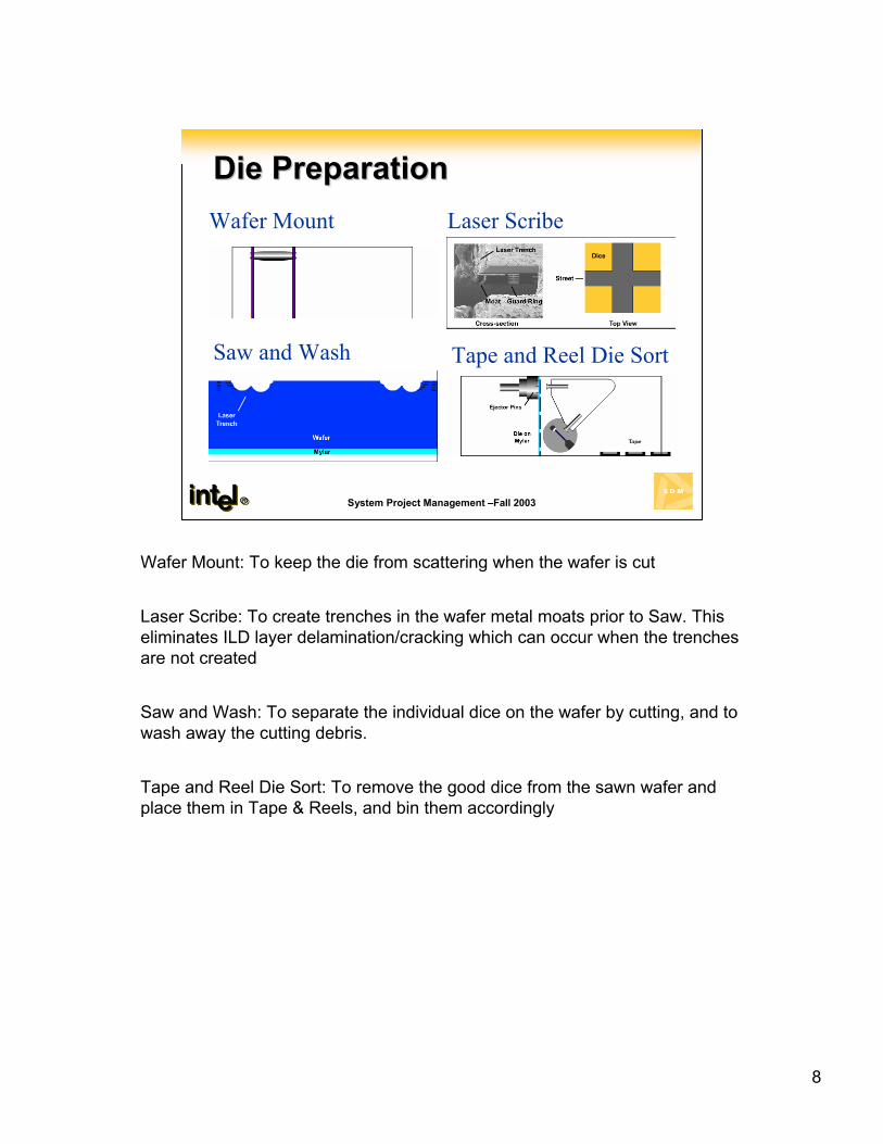
Die PreparationDie PreparationWafer Mount Laser Scribe
Saw and Wash Tape and Reel Die Sort
Wafer Mount: To keep the die from scattering when the wafer is cut
Laser Scribe: To create trenches in the wafer metal moats prior to Saw. This eliminates ILD layer delamination/cracking which can occur when the trenches are not created
Saw and Wash: To separate the individual dice on the wafer by cutting, and to wash away the cutting debris.
Tape and Reel Die Sort: To remove the good dice from the sawn wafer and place them in Tape & Reels, and bin them accordingly
8
System Project Management –Fall 2003
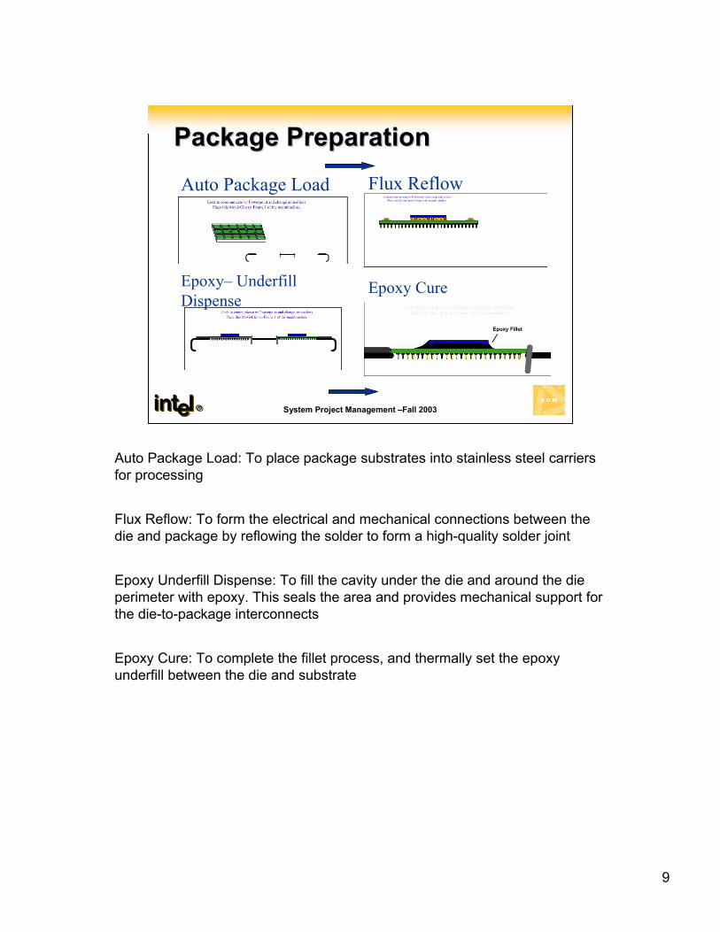
Package PreparationPackage PreparationAuto Package Load Flux Reflow
Epoxy– Underfill Dispense
Epoxy Cure
Auto Package Load: To place package substrates into stainless steel carriers for processing
Flux Reflow: To form the electrical and mechanical connections between the die and package by reflowing the solder to form a high-quality solder joint
Epoxy Underfill Dispense: To fill the cavity under the die and around the die perimeter with epoxy. This seals the area and provides mechanical support for the die-to-package interconnects
Epoxy Cure: To complete the fillet process, and thermally set the epoxy underfill between the die and substrate
9

System Project Management –Fall 2003
TestTest–– BurnBurn--InIn
Laser Mark Test– Burn-In
Post IHS Visual InspectionIHS–IHS Cure
IHS Cure: To thermally set the sealant and IHS Thermal Interface Material to provide a strong thermal and mechanical connection between the die and the heat spreader
IHS Visual Inspection: To inspect the packages to verify the IHS quality
Laser Mark: To scribe 2D matrix in the identifying information on the package. This step follows shortly after IHS because the IHS process covers the substrate mark
Burn In : Dies are tested at elevated temperatures and voltage to screen for infant mortality. Tests are run at low frequency (aim to ensure toggle coverage)
HIS=Integrated Heat Spreader
10

System Project Management –Fall 2003
Class Test and FusingClass Test and Fusing
PPVOff Line Fusing
Structural and Functional Test (Class)
Class (Structural and Functional Test): To perform 100% electrical test after Burn-In in order to isolate manufacturing defects, ensure product meets performance specifications per product data sheet, categorize components according to device performance (bins), and provide yield analysis/ improvement feedback for Fab & Assembly.
Fusing: To set the speed of the microprocessor by blowing a fuse in the circuitry that controls the device clock rate. This step is done here rather than at Test to postpone the configuration of the CPU to the latest point in the supply line. This gives Intel the most flexibility in setting the CPU performance based on a specific customer order
PPV: To verify that the microprocessors can run the various operating platforms they are designed to run (such as Windows, Unix, and OS/2). This is used to catch “test holes” (functional problems not caught at ST/FT Test).
11

Validation tests,& Design specs Design database
Fracture & Tapeout
Diagnose bugsightings
High-VolumeManufacturing
($$$)
Generate prod tests Mask, Fab, Pkg
Measure coverage& validate
Generate test prog
Si designValidation
Redesign
Workaround bugs
Debug
DE
Validation
PE
Factory
System Project Management –Fall 2003
Silicon Debug ProcessSilicon Debug ProcessValidation tests, & Design specs Design database
Fracture & Tapeout
Diagnose bugsightings
High-Volume Manufacturing
($$$)
Y
N
Generate prod tests Mask, Fab, Pkg
bugs?
Measure coverage& validate
CovgOK?
Generate test prog
Y
N
EngineeringSamples
Si designValidation Qual
Redesign
Workaround bugs
Debug
DE
ValidationLegend:
PE
Factory
Tester & Systems
Tests Validation Debug
PE: Product engineer DE: Design engineer
Silicon debug process involves close coordination between the design engineers, product engineers and the fab engineers. Time is of the essence and any design escape can be very expensive at this stage.
More than 1 year of preparation/planning is required before the first silicon comes through the fab for test/debug operations.
There are multiple iteration loops between first silicon and test/debug operations.
12

System Project Management –Fall 2003
Backend FlowBackend Flow1 2 3 4 5 6 7 8 9 10 11 12 13 14 15 16 17 18 19 20 21 22 23 24 25 26 27 28 29 30 31 32 33 34 35 36 37 38 39 40 41 42 43 44 45 46 47 48 49 50 51 52 53 54 55 56 57 58 59 60
1 Set customer target • x x • 2 Estimate sales volumes x • x x • 3 Establish pricing direction x • x • 4 Schedule project timeline • x 5 Development methods x • x x x x 6 Macro targets/constraints x x • x x x x 7 Financial analysis x x x x x • 8 Develop program map x • x 9 Create initial QFD matrix x x x x •
10 Set technical requirements x x x x • x 11 Write customer specification x x x x x • O O O O O O O O 12 High-level modeling x x x x • x x x 13 Write target specification x x x x x x x x x • x x 14 Develop test plan x x x x x • x 15 Develop validation plan x x x x • 16 Build base prototype x x x x x x • 17 Functional modeling x x x x x • x x x x x x x x O O O O O O O O O O 18 Develop product modules x x x x x x x x x • O 19 Lay out integration x x x x x x x x x • 20 Integration modeling x x x x x x x • x x x 21 Random testing x x • x x x 22 Develop test parameters x x x x x x x • x x x 23 Finalize schematics x x x x x • x x O O O O O 24 Validation simulation x x x x x x x • x x 25 Reliability modeling x x x x x • x 26 Complete product layout x x x x x • x x 27 Continuity verification x x x x x x • 28 Design rule check x x x • 29 Design package x x x x x • O O O O O O O 30 Generate masks x x x x • x O 31 Verify masks in fab x x x • 32 Run wafers x • x O 33 Sort wafers x • 34 Create test programs x • 35 Debug products x x x x x • O O O O O O O 36 Package products x x x • 37 Functionality testing x x x • 38 Send samples to customers x x x x • 39 Feedback from customers x • 40 Verify sample functionality x • 41 Approve packaged products x x x x • 42 Environmental validation x x x x • 43 Complete product validation x x x x x • 44 Develop tech. publications x x • x x 45 Develop service courses x x • x 46 Determine marketing name x x x x x • x 47 Licensing strategy x x x • 48 Create demonstration x x x x x x • 49 Confirm quality goals x x x x x • 50 Life testing x x x • x x 51 Infant mortality testing x x x x • x 52 Mfg. process stabilization x x x • O O 53 Develop field support plan x x • 54 Thermal testing x x x • 55 Confirm process standards x • x x 56 Confirm package standards x x x x x • x 57 Final certification x x x x x x x x x x x • 58 Volume production x x x • x 59 Prepare distribution network x x x x x x x x • 60 Deliver product to customers x x x x x x x x x •
x = Information Flows = Planned Iterations O = Unplanned Iterations • = Generational Learning
Concurrent Activity Blocks
Potential Iterations
Generational Learning
Sequential Activities
Backend Flow
Backed flow includes the iterative process of manufacturing and testing of a microprocessor. This is the key iterative process that is followed for performance improvement , yield enhancement and testing of a design.
13
System Project Management –Fall 2003
Design Structure MatrixDesign Structure Matrix
Des
ign
Exe
cutio
n
Des
ign
VVT
(Val
idat
ion,
Ver
ifica
tion,
Tes
ting)
Dat
abas
e Fr
eeze
Fr
actu
re s
tart
(lay
ers)
Frac
ture
com
plet
e (T
/O)
Ret
icle
Del
iver
y
Pol
y
Met
al 1
1st e
test
dat
a po
int
Firs
t Silic
on s
ort o
ut
1st a
ssem
bled
(pea
nut)
units
Lead
lot a
ssem
ble
units
to P
E
1st B
oot
Silic
on D
ebug
Sys
tem
Val
idat
ion
Com
patib
ility
Val
idat
ion
Qua
lity
Val
idat
ion
Ven
dor C
usto
mer
sam
ples
Ext
. Vol
ume
QS
CW
-VF
(Sam
ples
)
QV
exe
cutio
n co
mpl
ete
(PTQ
)
SV
exe
cute
com
plet
e (P
TQ)
CV
exec
ute
com
plet
e (P
TQ)
CM
V de
bug
com
plet
e
Pro
duct
ion
TP re
leas
ed to
VF
(PTQ
)
PTQ
with
out
goin
g D
PM
<=
DP
M G
oal
(PTQ
) P
rodu
ctio
n R
isk
star
t
Fab
conv
ersi
on
Firs
t Sor
t out
(Pro
duct
ion)
Test
Sta
rts (P
rodu
ctio
n)
1st p
rod
to C
W(P
rodu
ctio
n)
Pro
duct
ion
Cus
tom
er D
ock
Del
iver
y
Mar
ketin
g/Pr
oduc
tion
Laun
ch
DE Design Execution 0 0 0 0 0 0 0 0 0 DE Design VVT (Validation, Verification, Testing) 0 0 0 0 0 0 0 0 0 0 DE Database Freeze 0 0 0 0 0 0 0 0 0 0 0 IMO Fracture start (layers) 0 0 0 0 0 0 0 0 0 0 0 0 IMO Fracture complete (T/O) 0 0 0 IMO Reticle Delivery 0 0 0 0 0 0 0 0 0 0 0 TMG Poly 0 0 0 0 0 0 0 0 0 0 TMG Metal 1 0 0 0 0 0 0 0 0 0 0 0 TMG 1st etest data point 0 TMG First Silicon sort out 0 0 0 ATD 1st assembled (peanut) units 0 0 0 ATD Lead lot assemble units to PE 0 0 SV 1st Boot 0 0 0 PE Silicon Debug 0 0 0 0 0 0 0 0 0 0 PE System Validation 0 0 0 0 0 0 0 0 PE Compatibility Validation 0 0 0 0 0 QRE Quality Validation 0 0 0 0 Marketing Vendor Customer samples 0 0 0 0 Marketing Ext. Volume QS CW -VF (Samples) 0 0 0 0 0 QRE QV execution complete (PTQ) 0 0 0 0 0 0 Validation SV execute complete (PTQ) 0 0 0 0 0 Validation CV execute complete (PTQ) 0 0 0 0 0 0 Validation CMV debug complete 0 0 0 0 0 0 0 PE Production TP released to VF (PTQ) 0 0 0 0 0 0 0 0 0 QRE PTQ with outgoing DPM <= DPM Goal (PTQ) 0 0 0 0 0 0 0 0 0 0 PDT Production Risk start 0 0 0 0 0 0 0 0 0 0 0 0 TMG Fab conversion 0 0 0 0 0 0 0 0 0 0 0 0 0 TMG First Sort out (Production) 0 0 TMG Test Starts (Production) 0 0 TMG 1st prod to CW(Production) 0 0 ISNG Production Customer Dock Delivery 0 Marketing Marketing/Production Launch 0 0 0
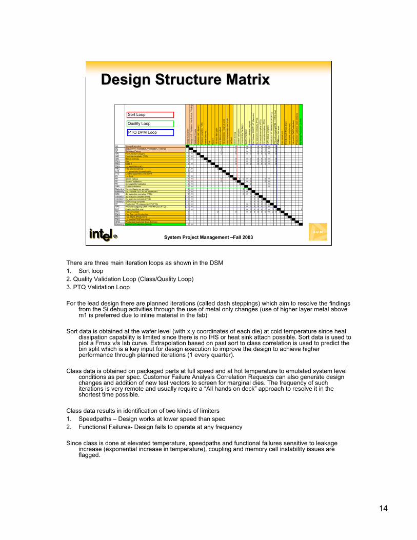
Sort Loop
PTQ DPM Loop
Quality Loop
There are three main iteration loops as shown in the DSM 1. Sort loop 2. Quality Validation Loop (Class/Quality Loop) 3. PTQ Validation Loop
For the lead design there are planned iterations (called dash steppings) which aim to resolve the findings from the Si debug activities through the use of metal only changes (use of higher layer metal above m1 is preferred due to inline material in the fab)
Sort data is obtained at the wafer level (with x,y coordinates of each die) at cold temperature since heat dissipation capability is limited since there is no IHS or heat sink attach possible. Sort data is used to plot a Fmax v/s Isb curve. Extrapolation based on past sort to class correlation is used to predict thebin split which is a key input for design execution to improve the design to achieve higher performance through planned iterations (1 every quarter).
Class data is obtained on packaged parts at full speed and at hot temperature to emulated system level conditions as per spec. Customer Failure Analysis Correlation Requests can also generate designchanges and addition of new test vectors to screen for marginal dies. The frequency of such iterations is very remote and usually require a “All hands on deck” approach to resolve it in the shortest time possible.
Class data results in identification of two kinds of limiters 1. Speedpaths – Design works at lower speed than spec 2. Functional Failures- Design fails to operate at any frequency
Since class is done at elevated temperature, speedpaths and functional failures sensitive to leakageincrease (exponential increase in temperature), coupling and memory cell instability issues are flagged.
14
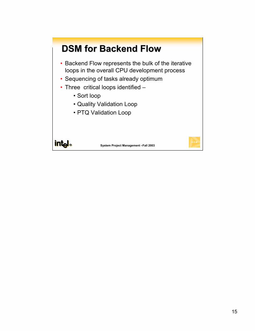
DSM for Backend FlowDSM for Backend Flow• Backend Flow represents the bulk of the iterative
loops in the overall CPU development process • Sequencing of tasks already optimum
• Three critical loops identified –
• Sort loop • Quality Validation Loop • PTQ Validation Loop
System Project Management –Fall 2003
15

Managing IterationsManaging Iterations –– PDT interactionsPDT interactions
JPT
Co-ordination Meetings
Program Ops
Meeting War
Room Forums
Stepping WG
Top Bin Design Process
Sync
PME
TME
ATMO
Prod Planner
ATM
Functional Groups
PDT
Stepping Conversion
NPP FSM
Pkg ATD Finance PDE Design PQRE Validation (CV, SV,
Design CMV, EV)
System Project Management –Fall 2003
PDT is the central coordinating body for all project management activitiesPDT is the central coordinating body for all project management activities
PDT Product Development Teams
PDT is the central coordinating body which has member participation from all functional groups. All decisions that affect engineering commitments must be discussed in Co-ordination Meeting or War Room.
Escalation Path: In the event of serious disagreement (e.g. project priority), the escalation path starts with Product Coordination Meeting, War Room or Program Ops Meeting, and may be forwarded to RDM if appropriate
Stepping WG focus on stepping specific issues. Stepping usually involve minor design changes to improve performance or functionality through either metal or all layer changes. (A1, A2, A3….Metal Only Changes B1, B2, B3….refer to all layer changes and make WIP useless)
Design Process Sync is weekly IPT whose primary focus is on design + process optimization to meet product roadmap (long range strategic planning/technical discussion forum)
16

Managing IterationsManaging Iterations
• Speedpath Czars • FMEA is done in parallel to disseminate learning to all
projects outside of critical path• Integration of on-die, design for test/manufacturing
features critical to reduce impact of iterations– Clock tuning, Metal options, Bonus devices, Software
controlled timing, DFT features… • Live Methodology Documents
–Updated through Techforum review • Design Forums
– Disseminate learning from backend flow to front enddesign
System Project Management –Fall 2003
17

Key LearningsKey Learnings• Intel has an inherited culture of relying on data driven,
IPT based approach in product development– IPT membership has required membership to manage
interactions effectively • Sequencing of tasks in the backend is optimized based
on past generation. • Unplanned Iterations are managed by
– Improved coordination through IPT –DFM, DFT features –Knowledge Sharing
• DSM adoption for new CPU projects can be critical to speed up NPI
System Project Management –Fall 2003
New Product Introduction (NPI)DFM = Design for manufacturing features DFT = Design for test features
18

19
System Project Management –Fall 2003
Clock Skew EliminationClock Skew Elimination
14 7 101316
19
17010
20
30
Skew
X locationY location
Global Clock Skew Across Die (Post-Compensation)
1 3 5 7 9 11 13 15 171
713
19 051015202530
Skew
X locationY location
Global Clock Skew Across Die (Pre-Compensation)
Clock compensation to tune skew critical minimizing impact of Clock compensation to tune skew critical minimizing impact of unplanned iterationsunplanned iterations
Intentional Skew
Pre Compensated Clock SkewDue to variation in channel length, threshold voltage, supply gradient and other device parameters, clock skew is introduced in the design.Compensation mechanism exist to correct this to reduce iterations post manufacturing as part of the test flow. The same mechanism is used to optimize the bin split at the highest frequency.As show here, the max skew of 30 ps is reduced to less than 10 ps through clock tree de-skewing. Note that the 10ps offset is intentional skew to maximize bin split.
Post Compensated Clock SkewZero-skew clock not always best for max-frequency on siliconDominant post-silicon paths may be isolated to a few clock domains or phase dependantGenetic algorithm developed on tester to run thousands of combinations skewing clock domains and duty cycle for best combination

RecommendationsRecommendations• Product launch plans can be pulled in through
improvements in Sort capability
– Use of Hot Sort capability can result in early bin split information (~2 weeks lead time reduction in getting Fmax/Isb data at hot temp)
– Enables changes to design earlier for new product launch sooner
• High Frequency of IPT meetings (daily) may impact normal work progress to some extent
System Project Management –Fall 2003
DFT = Design for test features like probe node area control diodes to enable laser voltage probing for silicon debug. Critical for functional and timing debug IPT = Integrated Product Teams
In the past due to daily frequency of War Rooms and high level of visibility inthese forums, there have been occasions wherein normal work processes were neglected just to sustain progress updates in the IPT forums. This can be really expensive in stalling work progress through normal work channels.
Use of Hot Sort capability enhancements enable us to get hot temperatureFmax/Isb data to predict functionality and speed/yield information at least 2 weeks early (This emulates class results which are obtained after packagedparts are available for testing). This enables early progress in making designchanges to fix functional or speedpath bugs. This can also assist in addition of tests to screen for marginal dies which fail at higher temperatures after class testing. This saves additional time since we can get a more robust testprogram for class ready before packaged parts arrive for testing.
Total effort saving is hence much more than 2 weeks (can be 2X of lead timesavings)
20

System Project Management –Fall 2003
Yield VariabilityYield Variability
Standby Current
Frequency
Cd = Critical dimension or channel length Based on Cd targets, the Standby current varies. Isb increases exponentially with Cd reduction Shorter Cd result in faster devices and higher frequency of operation
21

System Project Management –Fall 2003
Questions ?Questions ?
22

BackupBackup
System Project Management –Fall 2003
23

System Project Management –Fall 2003
Product Life CycleProduct Life Cycle
Backend Flow
Commitment of resources is managed from phase to phase Slanted lines between phases represent overlap of activities Each phase includes inputs, management approval and documented results Market and business needs drive the creation of product line families…
24
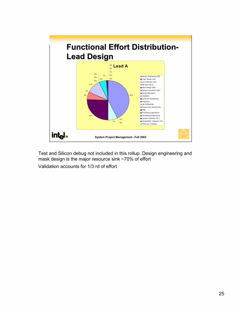
Functional Effort DistributionFunctional Effort Distribution--Lead DesignLead Design
Lead A
43%
0%
0%7%
26%
6%
0%
11%
0%
0%
0%
6%
1%
0%
0%
0%
0%
0% Design Engineering (DE)
Logic Design (LD)
Circuit Design (CD)
Microarchitects
Mask Design (MD)
Design Automation (DA)
Design Managers
Validation
Sof tw are Engineering
Integration
(DFT/DFD/DFM)
Product Dev Engineering
QRE
Test/Debug Operations
Test/Debug Engineering
System V alidation (SV)
Compatibility V alidation (CV )
Sof tw are V alidation
System Project Management –Fall 2003
Test and Silicon debug not included in this rollup. Design engineering and mask design is the major resource sink ~70% of effort Validation accounts for 1/3 rd of effort
25

System Project Management –Fall 2003
Speedpath Debug (10,000 Ft View)Speedpath Debug (10,000 Ft View)
Sort
Assembly & Packaging
Class
Wafer level test to screen bad die at low temperature
Full speed test at hot temperature on packaged parts
Speedpath identification
Isolated dies and limiting paths are used for directed debug on production testers
Directed tests and full production suite
Failure Analysis
Additional tests used for isolating worst case condition
Bug report filed Sighting database updated
ECO filed ECO Verification
ECO CommitTapeout
Tapeout FAB
Wafers Verified design database
Learning Dissemination
ECO: Engineering change order. Contains detailed bug information and proposed fix. Options to verify fix with metal options or software workaround listed. ECO Verification is done simultaneously through metal options under class testing and using simulation tools in the design database.
Learnings from each speedpath analysis are documented in a speedpath template and disseminated through design forums. Design rule checks are updated to verify entire database. Cross project wide dissemination of learnings is also enabled.
26
System Project Management –Fall 2003
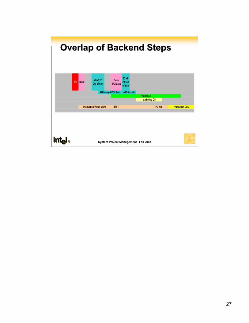
Overlap of Backend StepsOverlap of Backend Steps
T/O Mask Dash T/O/Mask
50 wfr P1 Out of Sort
Mtl 1
Marketing QS
Production Wafer Starts PG A/T Production CDD
50 wfr P1 Out of Sort
ATD Assy & PDL Test ATD Assy & Validation
27