Embed Size (px)
Citation preview
AVR447: Sinusoidal driving of three-phase permanent magnet motor using
ATmega48/88/168
Features � Three-phase sine waves
- 192 steps per electrical revolution - 8-bit amplitude resolution
� Software dead-time generation � Controlled by hall-sensors � Speed control through run-time scaling of sine wave amplitude
- Speed reference from analog input � Automatically synchronizes to a running motor at startup � Safe startup using block-commutation the first commutation steps � Direction controlled by digital input � Safe stop and direction change procedure
- Active braking or coasting during stopping � Advance commutation angle adjustable at run-time � Reverse rotation signal output � Tacho output signal
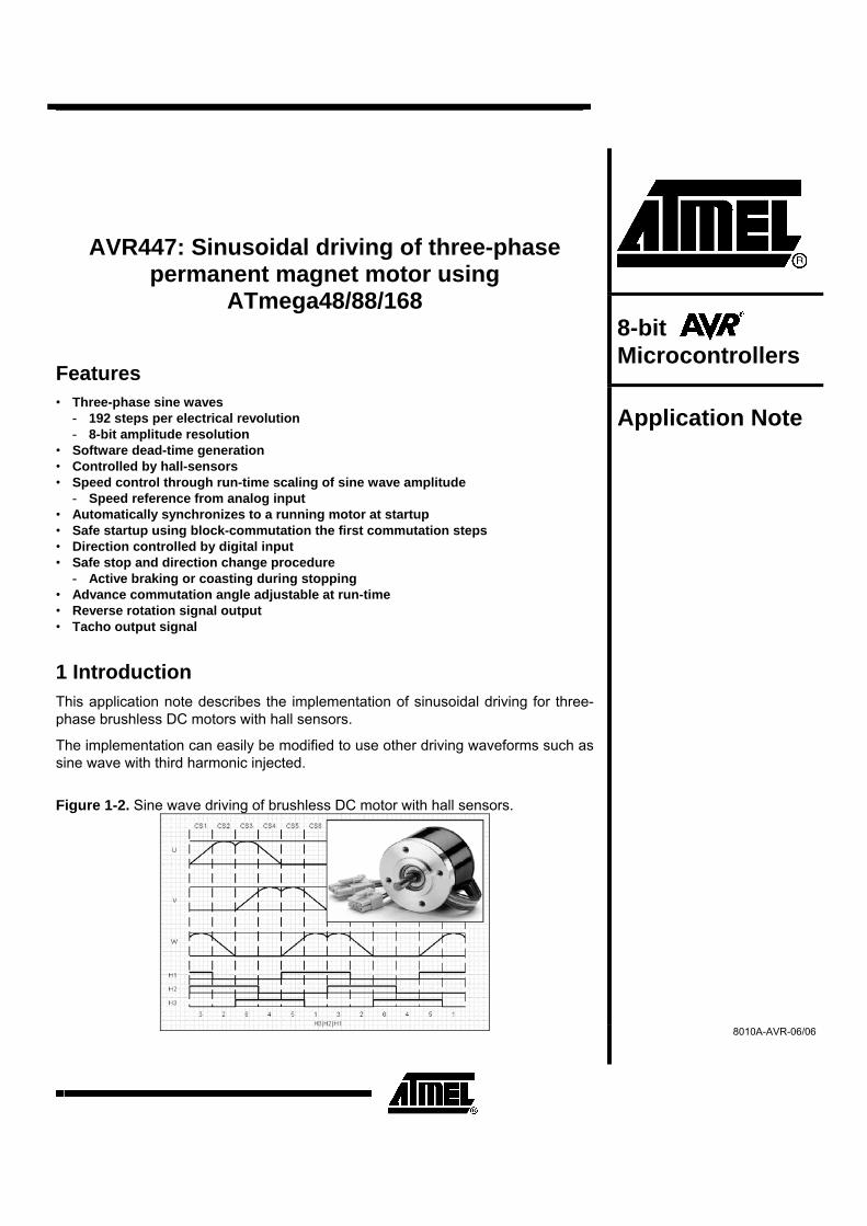
1 Introduction This application note describes the implementation of sinusoidal driving for three-phase brushless DC motors with hall sensors.
The implementation can easily be modified to use other driving waveforms such as sine wave with third harmonic injected.
Figure 1-2. Sine wave driving of brushless DC motor with hall sensors.
8-bit Microcontrollers Application Note
8010A-AVR-06/06
2 AVR447 8010A-AVR-06/06
2 Theory of operation In most of the literature, permanent magnet motors are divided into two categories based on the shape of the back-EMF (voltage induced in the coils when the motor is spinning). The back-EMF can either be trapezoidal or sinusoidal in shape. Although the terminology is not consistent throughout the literature, the majority seems to agree that a brushless DC motor (BLDC) has trapezoidal back-EMF, while a permanent magnet synchronous motor (PMSM) has sinusoidal back-EMF. Both BLDC and PMSM motors can be driven by sinusoidal currents, so there will not be made any distinction between them throughout this application note. Instead, they will both be referred to as a permanent magnet motor, or PMM.
3 Implementation on an AVR® This application note describes how to drive a three-phase PMM with sinusoidal currents. The code example can also be used as a general reference on how to generate waveforms using the PWM.
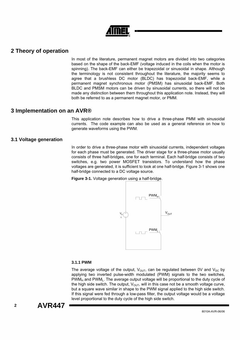
3.1 Voltage generation In order to drive a three-phase motor with sinusoidal currents, independent voltages for each phase must be generated. The driver stage for a three-phase motor usually consists of three half-bridges, one for each terminal. Each half-bridge consists of two switches, e.g. two power MOSFET transistors. To understand how the phase voltages are generated, it is sufficient to look at one half-bridge. Figure 3-1 shows one half-bridge connected to a DC voltage source.
Figure 3-1. Voltage generation using a half-bridge.
VD
C
PWMH
PWML
VOUT
3.1.1 PWM
The average voltage of the output, VOUT, can be regulated between 0V and VDC by applying two inverted pulse-width modulated (PWM) signals to the two switches, PWMH and PWML. The average output voltage will be proportional to the duty cycle of the high side switch. The output, VOUT, will in this case not be a smooth voltage curve, but a square wave similar in shape to the PWM signal applied to the high side switch. If this signal were fed through a low-pass filter, the output voltage would be a voltage level proportional to the duty cycle of the high side switch.
AVR447
3
8010A-AVR-06/06
For several reasons, it is not common to add a separate low-pass filter in motor control designs. First of all, the motor acts as a low pass filter. The inductance and resistance of the coils windings create a low pass RL filter. Further, the inertia of the rotor and load creates a mechanical low pass filter. Choosing the PWM switching frequency sufficiently high, there will be no noticeable jitter in the rotor speed. Secondly, the currents fed through the windings of even a small motor can be in the range of several amperes. Forcing this current through e.g. an RC filter would result in substantial power dissipation in the filter itself, an undesirable energy loss.
3.1.2 Dead-time
Switching devices, such as MOSFET transistors are not able to switch on and off instantly. Consider again the half-bridge from Figure 3-1. If the switches PWMH and PWML are fed with inverted signals, one switch will turn off at the same moment as the other switch turns on. During this transition, there will be a short time period where one switch has not completely closed while the other one is opening, making a direct connection between supply voltage and ground with very low resistance, allowing a large current to flow through the transistors. This situation is known as a shoot-through, and must be avoided, since it will probably destroy the driver stage if no hardware protection is in place.
The solution to this is to add a dead-time, a small time period where neither the high or low side switches are conducting, for every PWM transition.
3.1.3 Generating PWM signals with dead-time with an AVR
To understand how to implement PWM �voltage generation� with dead-time on an AVR, we continue to look at only one phase voltage. One timer/counter module on e.g. the ATmega48 can be used to control one half-bridge like the one in Figure 3-1. The timer/counter modules in the ATmega48 can control two PWM output pins each. The timer/counter units have several PWM modes, and there are several configuration options for the output pins.
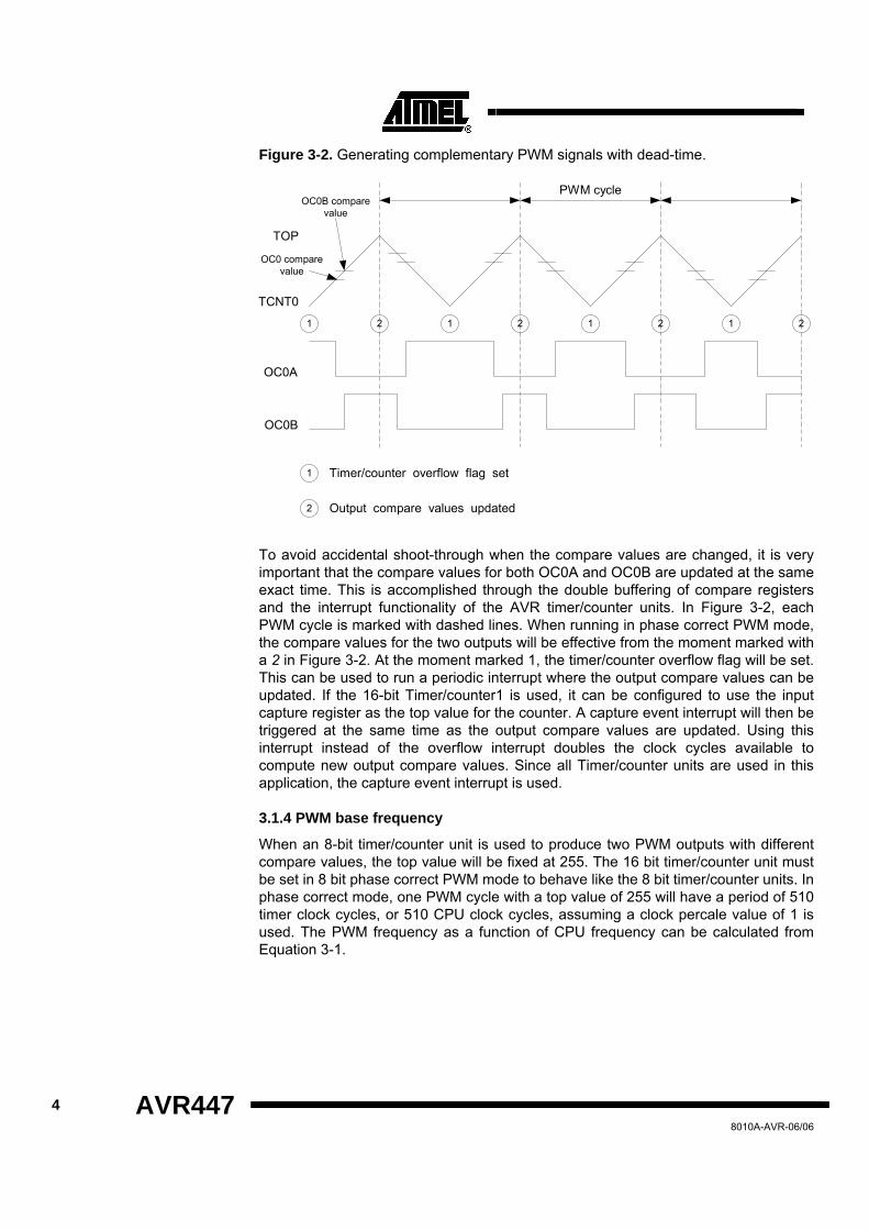
For the half-bridge control with dead-time, the phase correct PWM mode is very well suited. The counter works in a dual slope mode, which allows generation of center-aligned PWM signals with dead-time. Consider Figure 3-2 that shows how Timer/Counter0 can be set up to produce the desired signals. The triangular line represents the timer/counter value itself in the dual slope �phase correct mode�. In this example, the output pin OC0A has been configured to clear on compare match when up-counting and set on compare match when down-counting. This output will be connected to the high side switch of the half-bridge. Similarly, the output pin OC0B has been configured to set on compare match when up-counting and clear on compare match when down-counting. This output will be connected to the low-side switch of the half-bridge. Note that if the compare values for both outputs are set to the same value, the two outputs will be complementary. However, to insert a dead-time between the switching of the low and high side drivers, the compare values must be moved a little bit in each direction. Half the dead-time is subtracted from the OC0A compare value while the same amount is added to the OC0B compare value. This is illustrated by the short horizontal lines on the timer/counter curve in Figure 3-2. As can be seen from the OC0A and OC0B waveforms, the effect is that a dead-time of the same length is inserted at every PWM switching.
4 AVR447 8010A-AVR-06/06
Figure 3-2. Generating complementary PWM signals with dead-time.
TCNT0
OC0A
OC0B
PWM cycleOC0B compare
value
OC0 comparevalue
TOP
1 1 1 1
2
2 2 2
1 Timer/counter overflow flag set
Output compare values updated
2
To avoid accidental shoot-through when the compare values are changed, it is very important that the compare values for both OC0A and OC0B are updated at the same exact time. This is accomplished through the double buffering of compare registers and the interrupt functionality of the AVR timer/counter units. In Figure 3-2, each PWM cycle is marked with dashed lines. When running in phase correct PWM mode, the compare values for the two outputs will be effective from the moment marked with a 2 in Figure 3-2. At the moment marked 1, the timer/counter overflow flag will be set. This can be used to run a periodic interrupt where the output compare values can be updated. If the 16-bit Timer/counter1 is used, it can be configured to use the input capture register as the top value for the counter. A capture event interrupt will then be triggered at the same time as the output compare values are updated. Using this interrupt instead of the overflow interrupt doubles the clock cycles available to compute new output compare values. Since all Timer/counter units are used in this application, the capture event interrupt is used.
3.1.4 PWM base frequency
When an 8-bit timer/counter unit is used to produce two PWM outputs with different compare values, the top value will be fixed at 255. The 16 bit timer/counter unit must be set in 8 bit phase correct PWM mode to behave like the 8 bit timer/counter units. In phase correct mode, one PWM cycle with a top value of 255 will have a period of 510 timer clock cycles, or 510 CPU clock cycles, assuming a clock percale value of 1 is used. The PWM frequency as a function of CPU frequency can be calculated from Equation 3-1.
AVR447
5
8010A-AVR-06/06
Equation 3-1. PWM base frequency as a function of CPU frequency.
510CPU
PWMf
f =
3.2 Waveform generation Using the information from section 3.1 on how to set up the AVR to generate a voltage output from a half-bridge, it is possible to set up the system to drive a motor with a triple half-bridge.
3.2.1 Setting up the AVR
Each timer/counter unit on the ATmega48 is able to control one half-bridge, so all three timer/counter units are needed to control three half-bridges. Each timer is set up and connected to one half-bridge according to section 3.1. To make sure that the three timers are synchronized, each timer is preloaded with a value, since the three timers are started at a different moment. It is important to make sure that the three timers are synchronized, by e.g. running the application in simulation mode in AVR studio®, inspecting the values of the three timer registers.
3.2.2 Generating the waveforms
Three steps are involved in the calculation of the compare values for the three timer/counter units:
• Obtaining the desired output value
• Scaling the value to the desired amplitude
• Inserting the dead-time
The desired output value when driving a synchronous motor is a function of rotor position. The output values can either be calculated or stored in a look-up table. In this application note, a look-up table is used to store the values, to increase the performance of the application.
The values stored in the look-up table correspond to the maximum output amplitude. The look-up table value must be scaled down to the desired output amplitude. Equation 3-2 shows how the output value can be scaled. The output duty cycle, do, is obtained by multiplying the output value obtained from the look-up table, dtable, with a scaling factor, ks.
Equation 3-2. Amplitude scaling equation.
ntables
odk
d2
=
The output bit resolution can be calculated as no = nk + nt � n, where no, nk and nt are the bit resolutions of the output, scaling factor and table value respectively and n is the division exponent in Equation 3-2. E.g. a table value resolution of 8 bits, a scaling factor of 8 bits and a division exponent of 8 bits will generate an output duty cycle value with a bit resolution of 8 bits.
The dead-times are inserted as described in section 3.1.3. and the compare values can be output to the timer/counter compare registers.
These steps are repeated for every timer/counter overflow to update the outputs with the correct values with respect to rotor position.
6 AVR447 8010A-AVR-06/06
3.3 Generating sine waves Section 3.2 explains how to produce an arbitrary waveform stored in a look-up table. In this section, an efficient way to produce sine wave output is explained.
3.3.1 The output pattern
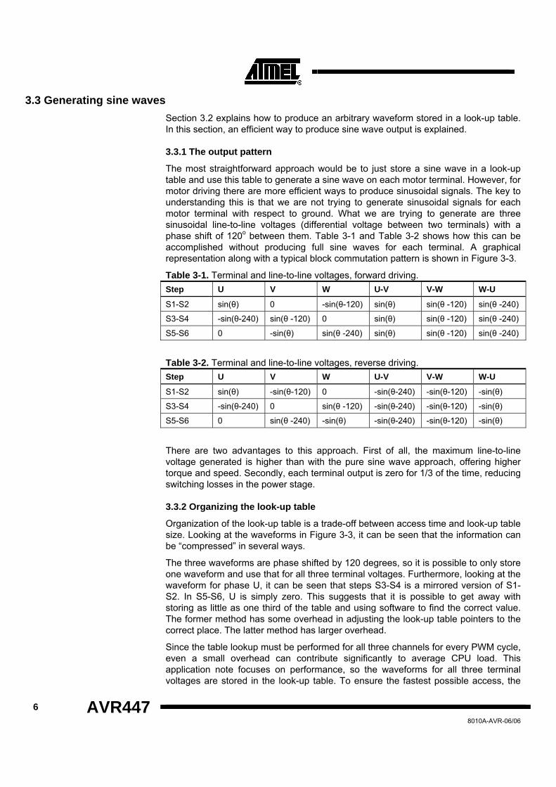
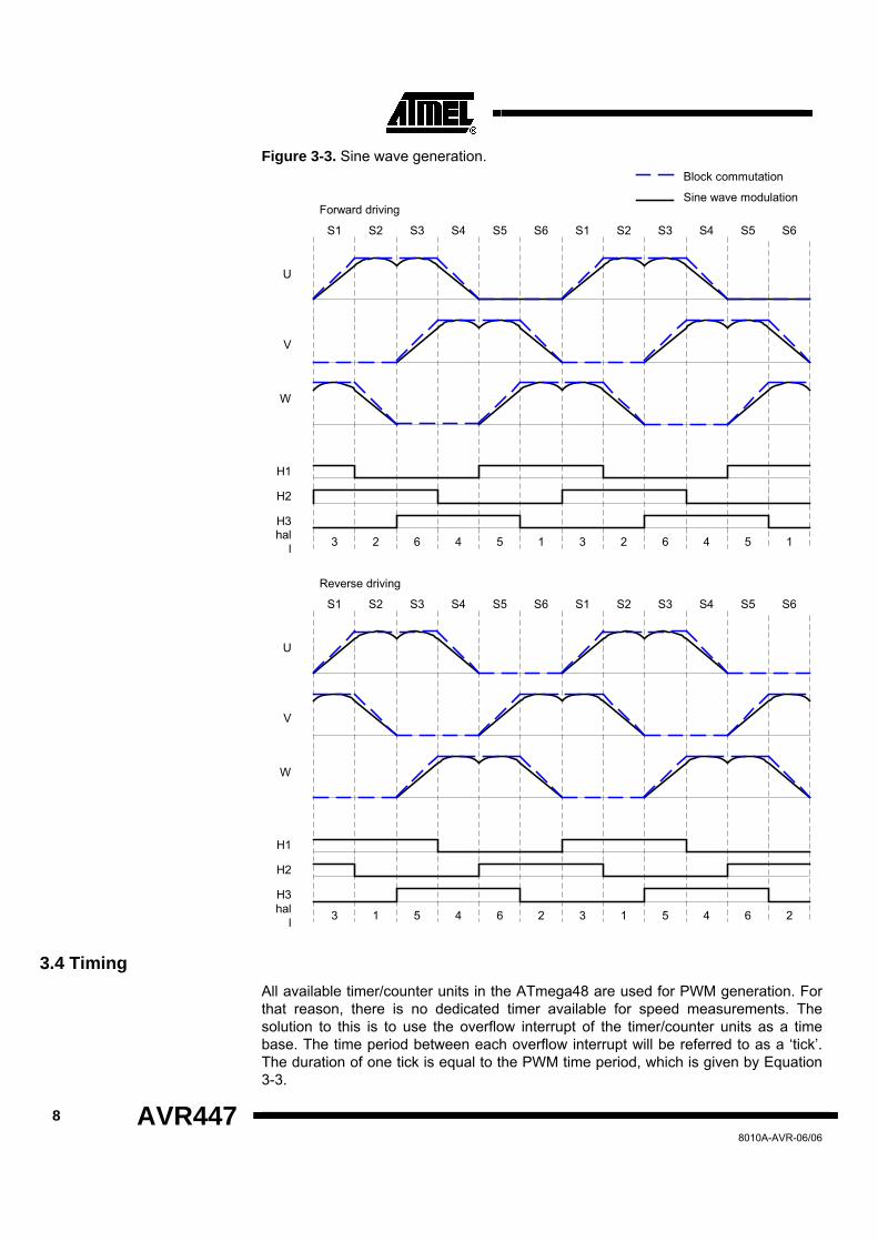
The most straightforward approach would be to just store a sine wave in a look-up table and use this table to generate a sine wave on each motor terminal. However, for motor driving there are more efficient ways to produce sinusoidal signals. The key to understanding this is that we are not trying to generate sinusoidal signals for each motor terminal with respect to ground. What we are trying to generate are three sinusoidal line-to-line voltages (differential voltage between two terminals) with a phase shift of 120o between them. Table 3-1 and Table 3-2 shows how this can be accomplished without producing full sine waves for each terminal. A graphical representation along with a typical block commutation pattern is shown in Figure 3-3.
Table 3-1. Terminal and line-to-line voltages, forward driving. Step U V W U-V V-W W-U
S1-S2 sin(θ) 0 -sin(θ-120) sin(θ) sin(θ -120) sin(θ -240)
S3-S4 -sin(θ-240) sin(θ -120) 0 sin(θ) sin(θ -120) sin(θ -240)
S5-S6 0 -sin(θ) sin(θ -240) sin(θ) sin(θ -120) sin(θ -240)
Table 3-2. Terminal and line-to-line voltages, reverse driving. Step U V W U-V V-W W-U
S1-S2 sin(θ) -sin(θ-120) 0 -sin(θ-240) -sin(θ-120) -sin(θ)
S3-S4 -sin(θ-240) 0 sin(θ -120) -sin(θ-240) -sin(θ-120) -sin(θ)
S5-S6 0 sin(θ -240) -sin(θ) -sin(θ-240) -sin(θ-120) -sin(θ)
There are two advantages to this approach. First of all, the maximum line-to-line voltage generated is higher than with the pure sine wave approach, offering higher torque and speed. Secondly, each terminal output is zero for 1/3 of the time, reducing switching losses in the power stage.
3.3.2 Organizing the look-up table
Organization of the look-up table is a trade-off between access time and look-up table size. Looking at the waveforms in Figure 3-3, it can be seen that the information can be �compressed� in several ways.
The three waveforms are phase shifted by 120 degrees, so it is possible to only store one waveform and use that for all three terminal voltages. Furthermore, looking at the waveform for phase U, it can be seen that steps S3-S4 is a mirrored version of S1-S2. In S5-S6, U is simply zero. This suggests that it is possible to get away with storing as little as one third of the table and using software to find the correct value. The former method has some overhead in adjusting the look-up table pointers to the correct place. The latter method has larger overhead.
Since the table lookup must be performed for all three channels for every PWM cycle, even a small overhead can contribute significantly to average CPU load. This application note focuses on performance, so the waveforms for all three terminal voltages are stored in the look-up table. To ensure the fastest possible access, the

AVR447
7
8010A-AVR-06/06
values are organized as shown in Table 3-3. This allows all 3 values to be read with the very fast LPM Z+ instruction. To get the output values for forward driving, the table is read in the sequence U, V, W, while in the reverse direction, the sequence U, W, V is used.
Table 3-3. Sine look-up table organization. U0 U0 - 120o U0 - 240o U1 U1 - 120o U1 - 240o �
8 AVR447 8010A-AVR-06/06
Figure 3-3. Sine wave generation.
S1 S2 S3 S4 S5 S6 S1 S2 S3 S4 S5 S6
U
V
W
S1 S2 S3 S4 S5 S6 S1 S2 S3 S4 S5 S6
U
V
W
Forward driving
Reverse driving
H1
H2
H3hal
l 3 2 6 4 5 1 3 2 6 4 5 1
hall
H1
H2
H3
3 1 5 4 6 2 3 1 5 4 6 2
Block commutation
Sine wave modulation
3.4 Timing All available timer/counter units in the ATmega48 are used for PWM generation. For that reason, there is no dedicated timer available for speed measurements. The solution to this is to use the overflow interrupt of the timer/counter units as a time base. The time period between each overflow interrupt will be referred to as a �tick�. The duration of one tick is equal to the PWM time period, which is given by Equation 3-3.
AVR447
9
8010A-AVR-06/06
Equation 3-3. PWM time period.
CPUPWMPWM ff
T 5101==
As an example, at 8MHz CPU clock, one tick has a duration of 63.75µs.
3.5 Position sensors and its usage Since the objective is to control a synchronous motor, some kind of information about the rotor position must be known in order to produce waveforms that are synchronized to the motor. This information can be obtained, e.g. by using a rotary encoder. However, many permanent magnet motors are equipped with three hall sensors mounted providing information about the rotor positions in 60 degree increments. In this application note, the hall sensors are used as the only position sensing devices.
In Figure 3-3, the three hall sensor signals are shown as H1, H2 and H3. The hall sensor inputs translates into a number between 1 and 6 by treating each of the hall sensor signals as binary digits and arranging them as hall = H3 H2 H1. The hall values corresponding to the different combinations of H3, H2 and H1 are shown in Figure 3-3.
The state of the hall sensors and the timing of hall sensor changes are used for several purposes:
• Output waveform phase locked loop
• Speed calculation
• Block commutation
• Rotation detection.
• Synchronization and direction change
• Advance commutation angle control
• Tacho output signal
3.5.1 Phase locked loop
The goal of the waveform generation is to keep the output waveforms synchronized to the rotation of the rotor. The challenge when using hall sensors as position sensors is that up-to-date information about rotor position is only available every 60 degrees. To solve this challenge, a phase locked loop must be implemented that keeps the output waveform in synch with the rotor.
An index (or pointer) into the look-up table is maintained at all times. The information obtained from the hall sensors is used to update this index.
The most accurate position information is available in the exact moment when a hall sensor changes value. At this point, the exact angle of the rotor is known.
In the time between hall sensor changes, no information about the position of the rotor is available. However, we do know the position of the rotor at the last hall sensor change, and we can measure the time period between the last two hall sensor changes. This allows us to calculate the speed of the rotor and, assuming constant speed, the position can be calculated from Equation 3-4.
10 AVR447 8010A-AVR-06/06
Equation 3-4. Position interpolation.
( ) tt ωθθωθ
+==
0
&
where θ is the angular position, θ0 is the angular position at the last hall sensor change, ω is the angular velocity and t is the time since the last hall sensor change.
Without going into detail, Equation 3-4 can be approximated by the difference equation shown in Equation 3-5.
Equation 3-5. Angular displacement difference equation. [ ] [ ] Tkk ωθθ +−= 1 ,
where θ is angular position, k is the current time step, ω is the angular velocity and T is the time step size.
In this application note, the angular position is represented by the look-up table index, measured in table steps. Time is measured in ticks. Angular velocity is defined by Equation 3-6.
Equation 3-6. Angular velocity definition
tΔΔ
=θω ,
where Δθ is the angular displacement during the time period Δt. Since angular displacement is measured in table steps and time is measured in ticks, the angular velocity unit is table steps per tick.
The look-up table index is updated once every tick, so the time step, T, of Equation 3-5 is 1 tick. The increment, used to iterate the table between two consecutive hall changes can thus be calculated from Equation 3-7.
Equation 3-7. Look-up table index increment calculation.
T
e
nn
Tt
Ti =ΔΔ
==θω ,
where ne is the number of table elements per commutation step (60 degrees of rotation) and nT is the number of ticks between the last two commutations.
At every tick, the increment is added to the look-up table index to update the position information.
The algorithm used to implement the phase locked loop can thus be summarized as:
1. At every hall sensor change:
o Set the look-up table index to correspond with the rotor position.
o Calculate the index increment from Equation 3-7.
2. For every tick until next hall sensor change:
o Update the look-up table index using Equation 3-5.
o Update PWM duty cycles according to look-up table index.
3. When hall sensors change, go back to 1.
AVR447
11
8010A-AVR-06/06
3.5.2 Speed calculation
If closed loop speed control is needed, the rotational speed of the motor must be calculated. As explained in section 3.5.1, the speed information is already calculated in the form of a look-up table increment value. There is no need to perform yet another computationally heavy calculation to obtain information about the speed. Nor is it necessary to have yet another variable with information about speed. Resources can be saved by representing other speed values, such as speed controller set-point in the same unit as the increment, since it corresponds directly to the speed information already available.
To control the speed to a certain RPM value, this value must first be converted to the corresponding increment value. It is therefore necessary to know the relationship between rotational speed and increment. Speed in revolutions per minute (RPM) is related to the number of ticks between hall sensor changes as shown in Equation 3-8.
Equation 3-8. RPM calculation.
T
CPU
RPM n
f
⋅
⋅=
51061
60ω
Rearranging to give ticks between hall changes as a function of speed:
Equation 3-9. Ticks between hall changes as a function of speed.
RPM
CPUt
fn
ω⋅⋅⋅
=510660
Combining Equation 3-7 and Equation 3-9 gives index increment as a function of speed (RPM):
Equation 3-10. Increment as a function of speed in RPM.
RPMCPU
e
fn
i ω⋅
⋅⋅=
605106
3.5.3 Block commutation
During the start-up phase, the speed of the rotor is not known until two subsequent hall sensor changes has been detected. To ensure a robust start-up, block commutation is used until the rotor speed is known. When operating in block commutation mode, all 6 PWM outputs are operated at the same duty cycle and commutation is controlled by enabling output of the PWM signals only to the pins that should be driven. The output pattern is updated at every hall change. One table for each direction is used to hold the output pattern values for the corresponding hall sensor inputs. For more information on driving a PMM with block commutation, refer to application note AVR443. The output pattern used in block commutation mode with respect to hall sensor input is also illustrated in Figure 3-3 along with the sinusoidal pattern.
3.5.4 Rotation detection
The sequence of hall sensor changes can be used to determine the actual direction of rotation. One table for each direction is used to store the next expected hall sensor value for each hall sensor value. This is used to deduce the actual direction of rotation.
12 AVR447 8010A-AVR-06/06
Comparing the actual direction of rotation to the commanded direction of rotation determines if the motor is spinning in the desired direction.
3.5.5 Synchronization and direction change
When the microcontroller is powered up or reset, the motor might already be spinning. It is therefore important that the firmware determines the state of the motor and synchronizes to this state.
When changing the direction of rotation, the rotor must first be stopped before it can be driven in the opposite direction. If the direction command is changed once again before the motor has stopped, the firmware must resynchronize before applying voltage to the terminals.
Synchronization and turning are controlled by the hall sensors. Direction information is deduced as described in section 3.5.4.
The motor is considered to be stopped when a sufficient number of ticks have passed since the last hall sensor change.
Synchronization occurs when the motor is spinning in the commanded direction and at least two hall sensor changes are detected.
3.5.6 Advance commutation control
A programmable advance commutation angle can be used to adjust the phase of the output waveform to make it lead the rotor angle. This might be necessary to get the motor to run at it�s maximum speed and/or efficiency. The advance commutation angle is run-time adjustable and can be set up to vary according to e.g. rotor speed or waveform amplitude. The advance commutation angle is obtained by adding an offset to the look-up table index, thus shifting the phase of the waveforms. The advance commutation angle can be adjusted in increments of 1 look-up table step (1.8û).
3.5.7 Tacho output signal
The tacho output signal is generated directly from the hall sensor input to produce a signal that reverses polarity for each hall sensor change.
3.6 Overcurrent detection A locked rotor, sudden load change or fast acceleration can cause excessive current to run through the motor and driver stage. In order to prevent damage due to over-current, it is very important to monitor current at all times. Usually, a shunt resistor is mounted between the driver stage transistors and ground, and the voltage across this shunt resistor is measured to calculate the current. This can be done with the ADC or an analog comparator.
In this application note, the ADC has been used to measure current. Using the ADC introduces a little delay, due to the conversion time, but there are other advantages. The analog comparator is on all the time, so it will be very sensitive to PWM switching noise, unless heavy external filtering is added. This problem is easier to overcome with the ADC. The voltage is sampled in one instant, and this instant can be triggered by e.g. an overflow event in a PWM timer (Point 1 in Figure 3-2), to make sure that the measurement is made at the same moment every PWM cycle. Unless the duty cycle is very low, this moment will also be far away from any PWM switching. The result is that less external filtering is needed to have reliable current measurements.
AVR447
13
8010A-AVR-06/06
3.7 Speed control This application note includes examples of both open loop speed control and a PID controller. It is also possible to add other kinds of speed regulators if desired. How to calculate the actual speed of the rotor was covered in section 3.5.2.
3.7.1 Speed reference
The controller, whether open or closed loop, needs some kind of speed reference. In this application note, an analog voltage reference is used, although it could easily be exchanged with e.g. a UART command. The analog reference is measured using the ADC.
3.7.2 Speed controller
It is possible to run the included firmware with open or closed loop speed control. The open loop speed control is very simple. The 8-bit analog speed reference value is directly used as the 8 bit amplitude value for the generated sine waves.
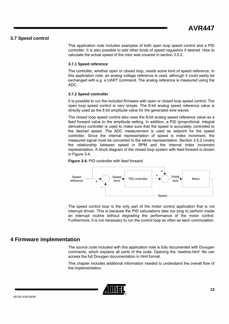
The closed loop speed control also uses the 8-bit analog speed reference value as a feed forward value to the amplitude setting. In addition, a PID (proportional, integral derivative) controller is used to make sure that the speed is accurately controlled to the desired speed. The ADC measurement is used as setpoint for the speed controller. Since the internal representation of speed is index increment, the measured signal must be converted to the same representation. Section 3.5.2 covers the relationship between speed in RPM and the internal index increment representation. A block diagram of the closed loop system with feed forward is shown in Figure 3-4.
Figure 3-4. PID controller with feed forward.
MotorPID controllerSpeederror
Speedreference
Speed
PWMduty
-+
++
The speed control loop is the only part of the motor control application that is not interrupt driven. This is because the PID calculations take too long to perform inside an interrupt routine without degrading the performance of the motor control. Furthermore, it is not necessary to run the control loop as often as each commutation.
4 Firmware implementation The source code included with this application note is fully documented with Doxygen comments, which explains all parts of the code. Opening the �readme.html� file can access the full Doxygen documentation in html format.
This chapter includes additional information needed to understand the overall flow of the implementation.
14 AVR447 8010A-AVR-06/06
4.1 Code structure Note that the code included with this application note has been written for high performance. Because of this, almost all source code is contained in one file to allow the compiler to optimize the code as much as possible. Most functions are declared with the �#pragma inline=forced� directive, since they are called from interrupt routines.
4.2 Peripheral usage The hardware peripherals in the ATmegax8 used in this application note are listed in Table 4-1.
Table 4-1. Hardware module usage. Hardware module Usage
Timer/counter0 Phase U PWM modulation
Timer/counter1 Phase V PWM modulation
Timer/counter2 Phase W PWM modulation
ADC channels Speed reference input/Current measurement
Pin change interrupt 0 Emergency shutdown interrupt
Pin change interrupt 1 Hall sensor change interrupt
Pin change interrupt 2 Direction change interrupt
4.3 Actions performed in interrupts The full motor control application, except speed control, is interrupt-based. Table 4-2 shows the responsibility of each interrupt used in the application. Understanding the responsibility of each interrupt service routine is the key to understanding how the application works.
AVR447
15
8010A-AVR-06/06
Table 4-2. Interrupt responsibility. Interrupt Function Responsibility/action Timer/counter1 capture event
Timer1CaptureISR PWM compare value update. Block commutation duty cycle control. Speed measurement. Stop detection.
Pin change 0 EmergencyInterruptISR External shut-off signal handling.
Pin change 1 HallChangeISR Synchronizes sine wave to hall sensors. Block commutation. Tacho output update. Actual direction detection. Detects whether firmware and motor are synchronized. Reverse rotation output signal update. Sine table index increment calculation. Stop detection.
Pin change 2 DirectionInputChangeISR Direction control input.
ADC complete ADCCompleteISR Sine wave amplitude/block commutation duty cycle control. Current measurements. ADC channel selection.
4.4 Output waveform generation Two interrupt service routines cooperate to produce the sine wave output. Timer1CaptureISR updates the PWM compare values once every PWM cycle. HallChangeISR synchronizes the sine wave to the current rotor position and calculates the sine table index increment. Figure 5-2 shows the interaction between the two ISRs. The state labeled �Any state� symbolizes that it is not relevant what state the motor was in or goes to.
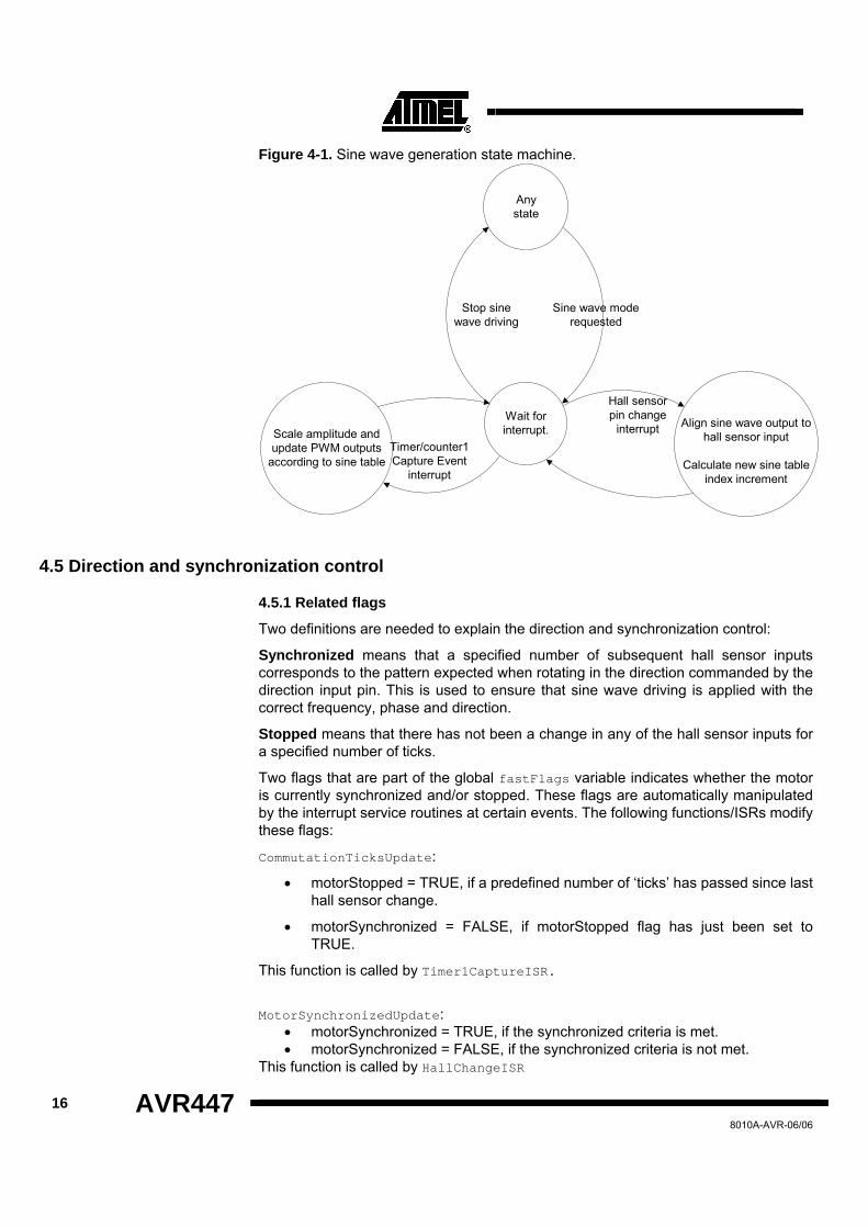
16 AVR447 8010A-AVR-06/06
Figure 4-1. Sine wave generation state machine.
Scale amplitude andupdate PWM outputs
according to sine table
Align sine wave output tohall sensor input
Calculate new sine tableindex increment
Wait forinterrupt.
Timer/counter1Capture Event
interrupt
Hall sensorpin change
interrupt
Anystate
Sine wave moderequested
Stop sinewave driving
4.5 Direction and synchronization control
4.5.1 Related flags
Two definitions are needed to explain the direction and synchronization control:
Synchronized means that a specified number of subsequent hall sensor inputs corresponds to the pattern expected when rotating in the direction commanded by the direction input pin. This is used to ensure that sine wave driving is applied with the correct frequency, phase and direction.
Stopped means that there has not been a change in any of the hall sensor inputs for a specified number of ticks.
Two flags that are part of the global fastFlags variable indicates whether the motor is currently synchronized and/or stopped. These flags are automatically manipulated by the interrupt service routines at certain events. The following functions/ISRs modify these flags:
CommutationTicksUpdate:
• motorStopped = TRUE, if a predefined number of �ticks� has passed since last hall sensor change.
• motorSynchronized = FALSE, if motorStopped flag has just been set to TRUE.
This function is called by Timer1CaptureISR.
MotorSynchronizedUpdate:
• motorSynchronized = TRUE, if the synchronized criteria is met. • motorSynchronized = FALSE, if the synchronized criteria is not met.
This function is called by HallChangeISR
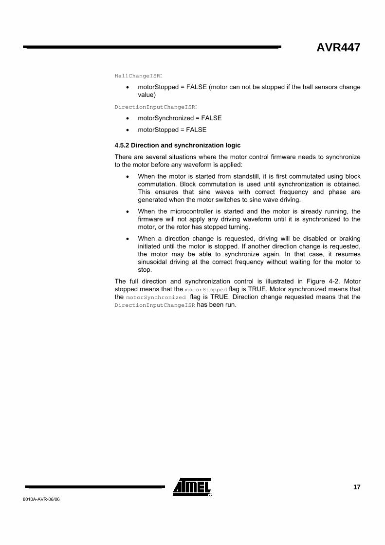
AVR447
17
8010A-AVR-06/06
HallChangeISR:
• motorStopped = FALSE (motor can not be stopped if the hall sensors change value)
DirectionInputChangeISR:
• motorSynchronized = FALSE
• motorStopped = FALSE
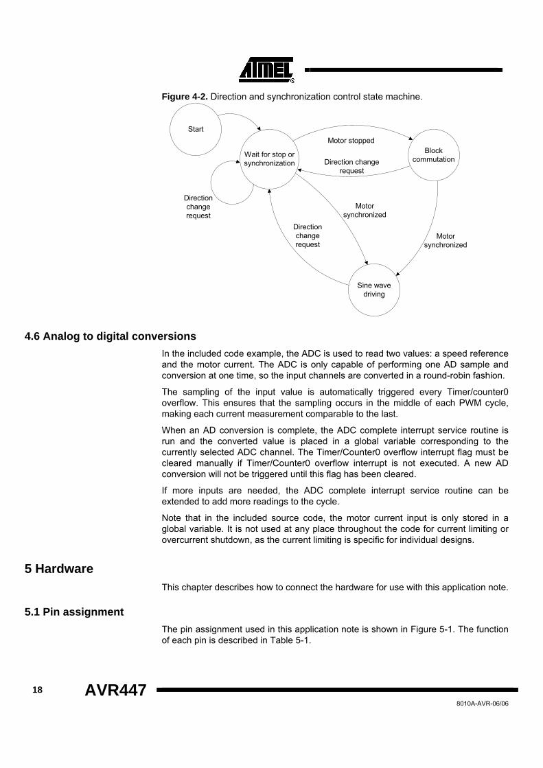
4.5.2 Direction and synchronization logic
There are several situations where the motor control firmware needs to synchronize to the motor before any waveform is applied:
• When the motor is started from standstill, it is first commutated using block commutation. Block commutation is used until synchronization is obtained. This ensures that sine waves with correct frequency and phase are generated when the motor switches to sine wave driving.
• When the microcontroller is started and the motor is already running, the firmware will not apply any driving waveform until it is synchronized to the motor, or the rotor has stopped turning.
• When a direction change is requested, driving will be disabled or braking initiated until the motor is stopped. If another direction change is requested, the motor may be able to synchronize again. In that case, it resumes sinusoidal driving at the correct frequency without waiting for the motor to stop.
The full direction and synchronization control is illustrated in Figure 4-2. Motor stopped means that the motorStopped flag is TRUE. Motor synchronized means that the motorSynchronized flag is TRUE. Direction change requested means that the DirectionInputChangeISR has been run.
18 AVR447 8010A-AVR-06/06
Figure 4-2. Direction and synchronization control state machine.
Wait for stop orsynchronization
Blockcommutation
Motor stopped
Sine wavedriving
Start
Directionchangerequest
Direction changerequest
Directionchangerequest
Motorsynchronized
Motorsynchronized
4.6 Analog to digital conversions In the included code example, the ADC is used to read two values: a speed reference and the motor current. The ADC is only capable of performing one AD sample and conversion at one time, so the input channels are converted in a round-robin fashion.
The sampling of the input value is automatically triggered every Timer/counter0 overflow. This ensures that the sampling occurs in the middle of each PWM cycle, making each current measurement comparable to the last.
When an AD conversion is complete, the ADC complete interrupt service routine is run and the converted value is placed in a global variable corresponding to the currently selected ADC channel. The Timer/Counter0 overflow interrupt flag must be cleared manually if Timer/Counter0 overflow interrupt is not executed. A new AD conversion will not be triggered until this flag has been cleared.
If more inputs are needed, the ADC complete interrupt service routine can be extended to add more readings to the cycle.
Note that in the included source code, the motor current input is only stored in a global variable. It is not used at any place throughout the code for current limiting or overcurrent shutdown, as the current limiting is specific for individual designs.
5 Hardware This chapter describes how to connect the hardware for use with this application note.
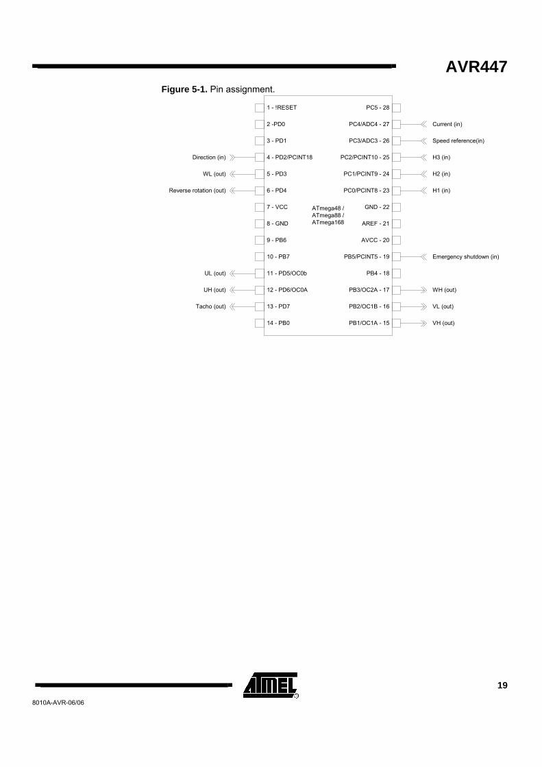
5.1 Pin assignment The pin assignment used in this application note is shown in Figure 5-1. The function of each pin is described in Table 5-1.
AVR447
19
8010A-AVR-06/06
Figure 5-1. Pin assignment.
ATmega48 /ATmega88 /ATmega168
1 - !RESET
2 -PD0
3 - PD1
4 - PD2/PCINT18
5 - PD3
6 - PD4
7 - VCC
8 - GND
9 - PB6
10 - PB7
11 - PD5/OC0b
12 - PD6/OC0A
13 - PD7
14 - PB0
PC5 - 28
PC4/ADC4 - 27
PC3/ADC3 - 26
PC2/PCINT10 - 25
PC1/PCINT9 - 24
PC0/PCINT8 - 23
GND - 22
AREF - 21
AVCC - 20
PB5/PCINT5 - 19
PB4 - 18
PB3/OC2A - 17
PB2/OC1B - 16
PB1/OC1A - 15
H3 (in)
H2 (in)
H1 (in)
UH (out)
UL (out)
VH (out)
VL (out)
WH (out)
WL (out)
Speed reference(in)
Emergency shutdown (in)
Direction (in)
Reverse rotation (out)
Tacho (out)
Current (in)
20 AVR447 8010A-AVR-06/06
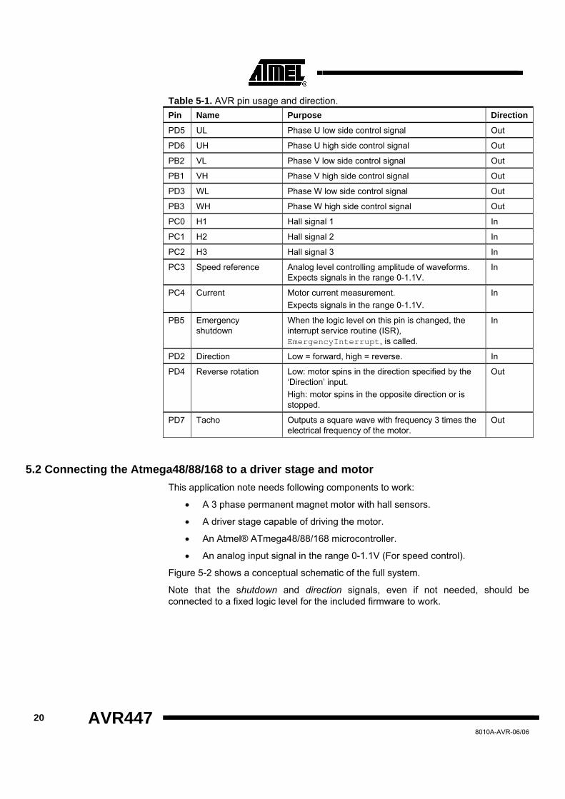
Table 5-1. AVR pin usage and direction. Pin Name Purpose Direction
PD5 UL Phase U low side control signal Out
PD6 UH Phase U high side control signal Out
PB2 VL Phase V low side control signal Out
PB1 VH Phase V high side control signal Out
PD3 WL Phase W low side control signal Out
PB3 WH Phase W high side control signal Out
PC0 H1 Hall signal 1 In
PC1 H2 Hall signal 2 In
PC2 H3 Hall signal 3 In
PC3 Speed reference Analog level controlling amplitude of waveforms. Expects signals in the range 0-1.1V.
In
PC4 Current Motor current measurement. Expects signals in the range 0-1.1V.
In
PB5 Emergency shutdown
When the logic level on this pin is changed, the interrupt service routine (ISR), EmergencyInterrupt, is called.
In
PD2 Direction Low = forward, high = reverse. In
PD4 Reverse rotation Low: motor spins in the direction specified by the �Direction� input. High: motor spins in the opposite direction or is stopped.
Out
PD7 Tacho Outputs a square wave with frequency 3 times the electrical frequency of the motor.
Out
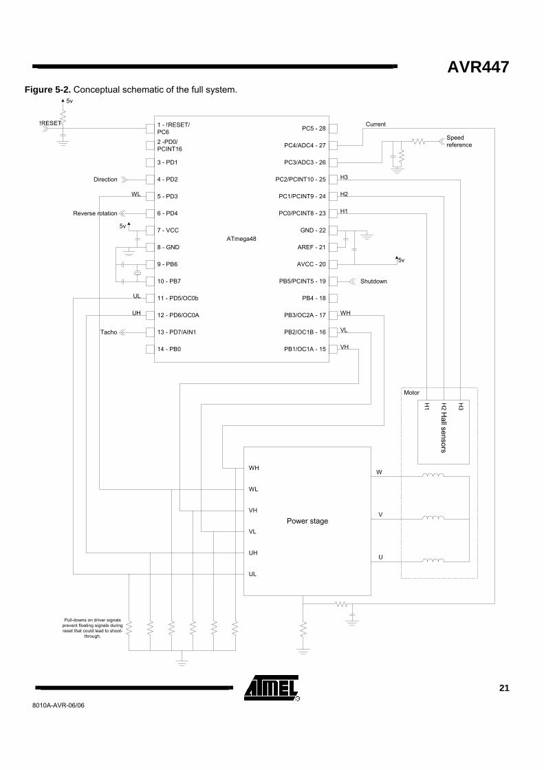
5.2 Connecting the Atmega48/88/168 to a driver stage and motor This application note needs following components to work:
• A 3 phase permanent magnet motor with hall sensors.
• A driver stage capable of driving the motor.
• An Atmel® ATmega48/88/168 microcontroller.
• An analog input signal in the range 0-1.1V (For speed control).
Figure 5-2 shows a conceptual schematic of the full system.
Note that the shutdown and direction signals, even if not needed, should be connected to a fixed logic level for the included firmware to work.
AVR447
21
8010A-AVR-06/06
Figure 5-2. Conceptual schematic of the full system.
ATmega48
1 - !RESET/PC62 -PD0/PCINT16
3 - PD1
4 - PD2
5 - PD3
6 - PD4
7 - VCC
8 - GND
9 - PB6
10 - PB7
11 - PD5/OC0b
12 - PD6/OC0A
13 - PD7/AIN1
14 - PB0
PC5 - 28
PC4/ADC4 - 27
PC3/ADC3 - 26
PC2/PCINT10 - 25
PC1/PCINT9 - 24
PC0/PCINT8 - 23
GND - 22
AREF - 21
AVCC - 20
PB5/PCINT5 - 19
PB4 - 18
PB3/OC2A - 17
PB2/OC1B - 16
PB1/OC1A - 15
H3
H2
H1
UH
UL
VH
VL
WH
WL
Power stage
UL
UH
VL
VH
WL
WH
5v
5v
!RESET
W
V
U
Speedreference
5v
Direction
Shutdown
Reverse rotation
Tacho
Pull-downs on driver signalsprevent floating signals duringreset that could lead to shoot-
through.
Motor
Hall sensors
H3
H2
H1
Current
22 AVR447 8010A-AVR-06/06
5.2.1 Using the ATAVRMC100 driver stage
This application note has been tested on the ATAVRMC100 power stage/motor development kit. The ATAVRMC100 has an onboard AT90PWM3 microcontroller mounted, but it is possible to use it as a power stage with a different microcontroller through the EXT_DRV and SENSOR interfaces on the board. The EXT_DRV header is documented in the ATAVRMC100 Hardware User Guide, available from the Atmel web site. It is important to erase the AT90PWM3 before using the ATAVRMC100 with a different microcontroller to ensure that only one microcontroller drives the signals.
Table 5-2 contains a complete list of the signals that must be connected to the ATAVRMC100 board. Note that the GND signal is connected to the negative shunt terminal, which is actually directly connected to ground. Figure 5-3 shows a graphical representation of the EXT_DRV header.
Table 5-3 shows the connections necessary to interface with the hall sensors. A graphical representation of this interface is shown in Figure 5-4.
AVR447
23
8010A-AVR-06/06
Table 5-2. ATAVRMC100 EXT_DRV connections. Signal name ATmegax8 pin ATAVRMC100 signal EXT_DRV pin number UH PD6 H_A 1
UL PD5 L_A 2
VH PB1 H_B 3
VL PB2 L_B 4
WH PB3 H_C 5
WL PD3 L_C 6
Current PC4 V shunt+ 7
GND GND V shunt- 8 Figure 5-3. EXT_DRV connection.
UL
VL
WL
GN
D
UH
VH
WH
Cur
rent
Table 5-3. ATAVRMC100 hall sensor interface. Signal name ATmegax8 pin ATAVRMC100 signal
H1 PC0 Sensor A
H2 PC1 Sensor B
H3 PC2 Sensor C
24 AVR447 8010A-AVR-06/06
Figure 5-4. Hall sensor connection.
H1
H2
H3A
BCS
enso
r
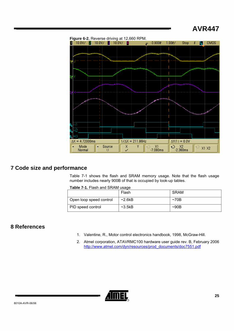
6 Waveform plots Figure 6-1 and Figure 6-2 show the waveforms generated when driving forward and reverse at different speeds. The average function on the oscilloscope has been used to smooth the waveforms. Both plots show, from the top: phase voltages for U, V, W, the line-to-line voltage U-V, then hall sensors H1, H2 and H3.
Figure 6-1. forward driving at 750 RPM.
AVR447
25
8010A-AVR-06/06
Figure 6-2. Reverse driving at 12,660 RPM.
7 Code size and performance Table 7-1 shows the flash and SRAM memory usage. Note that the flash usage number includes nearly 900B of that is occupied by look-up tables.
Table 7-1. Flash and SRAM usage Flash SRAM
Open loop speed control ~2.6kB ~70B
PID speed control ~3.5kB ~90B
8 References 1. Valentine, R., Motor control electronics handbook, 1998, McGraw-Hill.
2. Atmel corporation, ATAVRMC100 hardware user guide rev. B, February 2006 http://www.atmel.com/dyn/resources/prod_documents/doc7551.pdf
8010A-AVR-06/06
Disclaimer Atmel Corporation
2325 Orchard Parkway San Jose, CA 95131, USA Tel: 1(408) 441-0311 Fax: 1(408) 487-2600
Regional Headquarters Europe
Atmel Sarl Route des Arsenaux 41 Case Postale 80 CH-1705 Fribourg Switzerland Tel: (41) 26-426-5555 Fax: (41) 26-426-5500
Asia Room 1219 Chinachem Golden Plaza 77 Mody Road Tsimshatsui East Kowloon Hong Kong Tel: (852) 2721-9778 Fax: (852) 2722-1369
Japan 9F, Tonetsu Shinkawa Bldg. 1-24-8 Shinkawa Chuo-ku, Tokyo 104-0033 Japan Tel: (81) 3-3523-3551 Fax: (81) 3-3523-7581
Atmel Operations Memory
2325 Orchard Parkway San Jose, CA 95131, USA Tel: 1(408) 441-0311 Fax: 1(408) 436-4314
Microcontrollers 2325 Orchard Parkway San Jose, CA 95131, USA Tel: 1(408) 441-0311 Fax: 1(408) 436-4314 La Chantrerie BP 70602 44306 Nantes Cedex 3, France Tel: (33) 2-40-18-18-18 Fax: (33) 2-40-18-19-60
ASIC/ASSP/Smart Cards Zone Industrielle 13106 Rousset Cedex, France Tel: (33) 4-42-53-60-00 Fax: (33) 4-42-53-60-01 1150 East Cheyenne Mtn. Blvd. Colorado Springs, CO 80906, USA Tel: 1(719) 576-3300 Fax: 1(719) 540-1759 Scottish Enterprise Technology Park Maxwell Building East Kilbride G75 0QR, Scotland Tel: (44) 1355-803-000 Fax: (44) 1355-242-743
RF/Automotive Theresienstrasse 2 Postfach 3535 74025 Heilbronn, Germany Tel: (49) 71-31-67-0 Fax: (49) 71-31-67-2340 1150 East Cheyenne Mtn. Blvd. Colorado Springs, CO 80906, USA Tel: 1(719) 576-3300 Fax: 1(719) 540-1759
Biometrics/Imaging/Hi-Rel MPU/ High Speed Converters/RF Datacom
Avenue de Rochepleine BP 123 38521 Saint-Egreve Cedex, France Tel: (33) 4-76-58-30-00 Fax: (33) 4-76-58-34-80
Literature Requests
www.atmel.com/literature
Disclaimer: The information in this document is provided in connection with Atmel products. No license, express or implied, by estoppel or otherwise, to any intellectual property right is granted by this document or in connection with the sale of Atmel products. EXCEPT AS SET FORTH IN ATMEL’S TERMS AND CONDITIONS OF SALE LOCATED ON ATMEL’S WEB SITE, ATMEL ASSUMES NO LIABILITY WHATSOEVER AND DISCLAIMS ANY EXPRESS, IMPLIED OR STATUTORY WARRANTY RELATING TO ITS PRODUCTS INCLUDING, BUT NOT LIMITED TO, THE IMPLIED WARRANTY OF MERCHANTABILITY, FITNESS FOR A PARTICULAR PURPOSE, OR NON-INFRINGEMENT. IN NO EVENT SHALL ATMEL BE LIABLE FOR ANY DIRECT, INDIRECT, CONSEQUENTIAL, PUNITIVE, SPECIAL OR INCIDENTAL DAMAGES (INCLUDING, WITHOUT LIMITATION, DAMAGES FOR LOSS OF PROFITS, BUSINESS INTERRUPTION, OR LOSS OF INFORMATION) ARISING OUT OF THE USE OR INABILITY TO USE THIS DOCUMENT, EVEN IF ATMEL HAS BEEN ADVISED OF THE POSSIBILITY OF SUCH DAMAGES. Atmel makes no representations or warranties with respect to the accuracy or completeness of the contents of this document and reserves the right to make changes to specifications and product descriptions at any time without notice. Atmel does not make any commitment to update the information contained herein. Unless specifically provided otherwise, Atmel products are not suitable for, and shall not be used in, automotive applications. Atmel�s products are not intended, authorized, or warranted for use as components in applications intended to support or sustain life. © 2006 Atmel Corporation. All rights reserved. Atmel®, logo and combinations thereof, Everywhere You Are®, AVR®, AVR Studio® and others, are the registered trademarks or trademarks of Atmel Corporation or its subsidiaries. Other terms and product names may be trademarks of others.


![6HPHVWHU 7LPH WDEOH ZHI -XQH $ 17 · 2020. 6. 25. · 0v /lp /3 0v 1dl +& 0gp :dqj )dqj 55 6fl 1$ 0v (ol]d /rz 0v /lp 6/ 55 (/ 1$ 0v -hqqlihu :x +rph#:: 0u -hiiuh\ &kxd 0v ,y\ 1\dp](https://img.pdfslide.us/doc/110x75/5fd5d0796b0c65670c415668/6hphvwhu-7lph-wdeoh-zhi-xqh-17-2020-6-25-0v-lp-3-0v-1dl-0gp-dqj.jpg)