Embed Size (px)
Citation preview
14/12/2006 1001 Logic Gates & Transistors 1
1002 Logic gates and Transistors
Peter Rounce - room [email protected]
14/12/2006 1001 Logic Gates & Transistors 2
Metals - an electron is released by each metal atom to form electron `soup'.Applying an electric field across metal moves electron soup: a current flows.
Insulators - atoms in insulators keep all their electrons firmly attached.No electron 'soup' is created, and no current will flow in response to an applied electric field.
Semiconductors: these are normally weakly conducting when pure, conduction can be increased by 'doping': adding other materials.
Silicon doped with phosphorus atoms produces an n-type material:n-types semiconductors: electrons carry current.
Silicon doped with boron atoms produces a p-type material:p-type semiconductors: 'holes' carry current.
Materials
14/12/2006 1001 Logic Gates & Transistors 3
+++
+
+
+
++
++
++
holes
current
electrons
n-typep-type
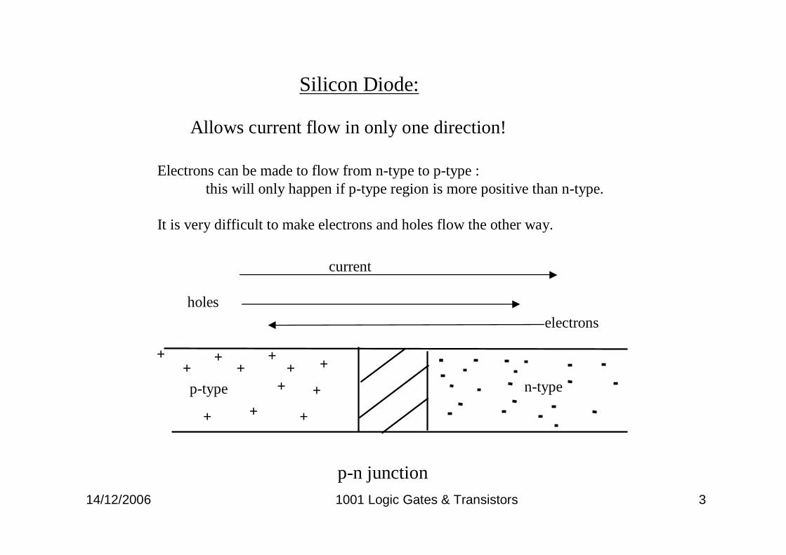
p-n junction
Allows current flow in only one direction!
Electrons can be made to flow from n-type to p-type :this will only happen if p-type region is more positive than n-type.
It is very difficult to make electrons and holes flow the other way.
Silicon Diode:
14/12/2006 1001 Logic Gates & Transistors 4
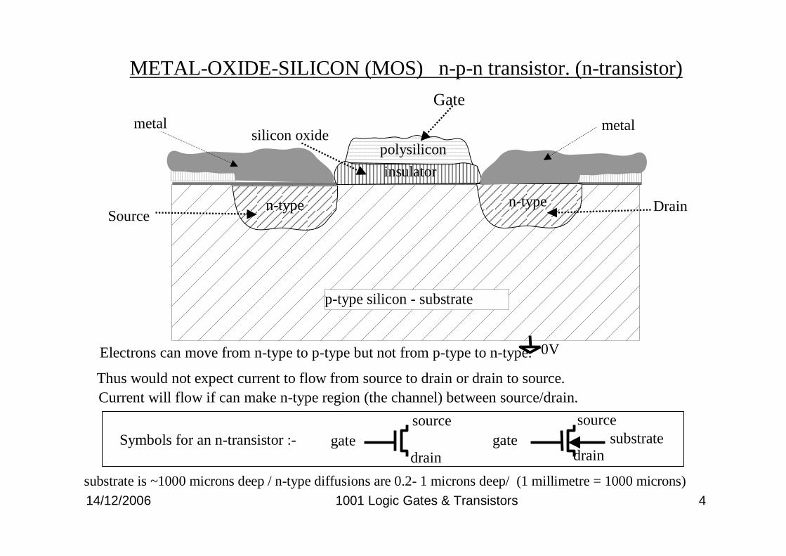
p-type silicon - substrate
Electrons can move from n-type to p-type but not from p-type to n-type.
Thus would not expect current to flow from source to drain or drain to source.Current will flow if can make n-type region (the channel) between source/drain.
polysilicon
n-typen-type
insulator
silicon oxide
Gate
0V
SourceDrain
metal metal
METAL-OXIDE-SILICON (MOS) n-p-n transistor. (n-transistor)
substrate is ~1000 microns deep / n-type diffusions are 0.2- 1 microns deep/ (1 millimetre = 1000 microns)
gatesource
draingate
source
drainsubstrateSymbols for an n-transistor :-
14/12/2006 1001 Logic Gates & Transistors 5
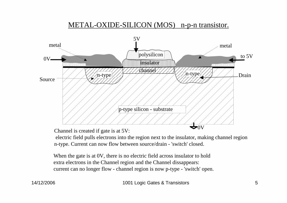
p-type silicon - substrate
polysilicon
n-typen-type
insulator
0V
SourceDrain
metal metal
channel
METAL-OXIDE-SILICON (MOS) n-p-n transistor.
Channel is created if gate is at 5V:electric field pulls electrons into the region next to the insulator, making channel region n-type. Current can now flow between source/drain - 'switch' closed.
When the gate is at 0V, there is no electric field across insulator to holdextra electrons in the Channel region and the Channel dissappears:current can no longer flow - channel region is now p-type - 'switch' open.
0V to 5V
5V
14/12/2006 1001 Logic Gates & Transistors 6
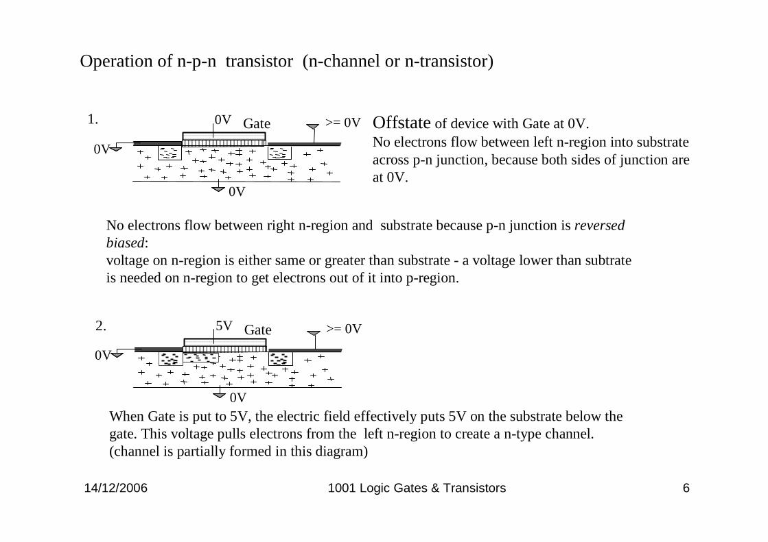
0V
>= 0V
0V
Gate0V1.
0V
>= 0V
0V
Gate5V2.
When Gate is put to 5V, the electric field effectively puts 5V on the substrate below the gate. This voltage pulls electrons from the left n-region to create a n-type channel. (channel is partially formed in this diagram)
Operation of n-p-n transistor (n-channel or n-transistor)
Offstateof device with Gate at 0V.No electrons flow between left n-region into substrate across p-n junction, because both sides of junction are at 0V.
No electrons flow between right n-region and substrate because p-n junction is reversed biased: voltage on n-region is either same or greater than substrate - a voltage lower than subtrateis needed on n-region to get electrons out of it into p-region.
14/12/2006 1001 Logic Gates & Transistors 7
Operation of n-p-n transistor (n-channel or n-transistor)
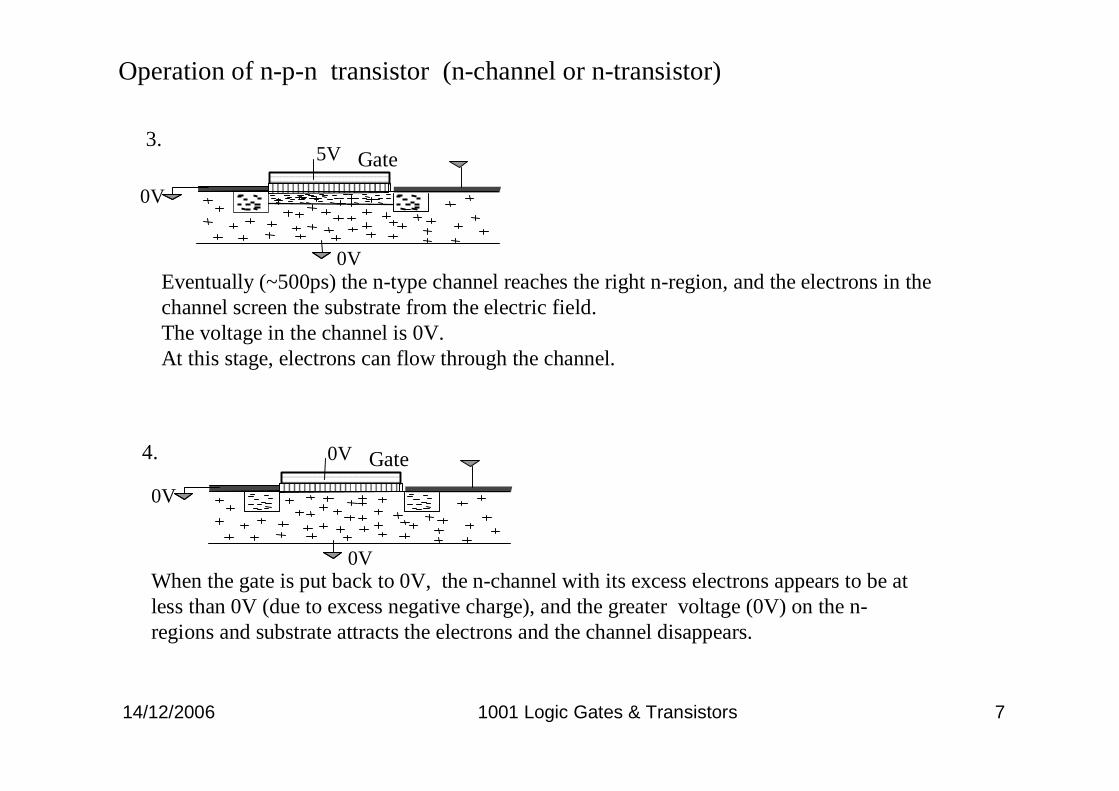
Eventually (~500ps) the n-type channel reaches the right n-region, and the electrons in the channel screen the substrate from the electric field. The voltage in the channel is 0V. At this stage, electrons can flow through the channel.
0V
0V
Gate5V3.
0V
0V
Gate0V4.
When the gate is put back to 0V, the n-channel with its excess electrons appears to be at less than 0V (due to excess negative charge), and the greater voltage (0V) on the n-regions and substrate attracts the electrons and the channel disappears.
14/12/2006 1001 Logic Gates & Transistors 8
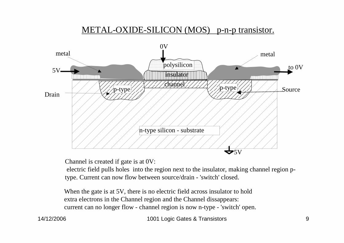
n-type silicon - substrate
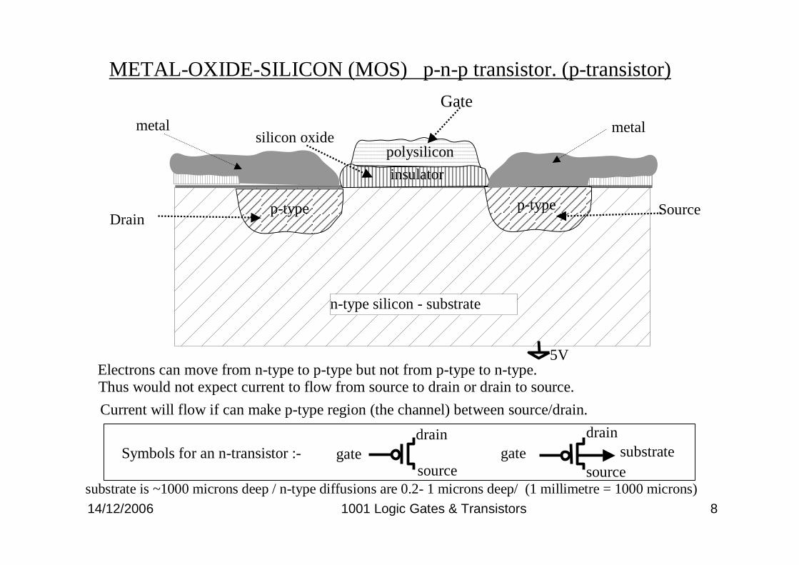
Electrons can move from n-type to p-type but not from p-type to n-type.Thus would not expect current to flow from source to drain or drain to source.
Current will flow if can make p-type region (the channel) between source/drain.
polysilicon
p-typep-type
insulator
silicon oxide
Gate
5V
DrainSource
metal metal
METAL-OXIDE-SILICON (MOS) p-n-p transistor. (p-transistor)
substrate is ~1000 microns deep / n-type diffusions are 0.2- 1 microns deep/ (1 millimetre = 1000 microns)
gatesource
draingate
source
drainsubstrateSymbols for an n-transistor :-
14/12/2006 1001 Logic Gates & Transistors 9
n-type silicon - substrate
polysilicon
p-typep-type
insulator
5V
DrainSource
metal metal
Channel is created if gate is at 0V:electric field pulls holes into the region next to the insulator, making channel region p-type. Current can now flow between source/drain - 'switch' closed.
channel
METAL-OXIDE-SILICON (MOS) p-n-p transistor.
When the gate is at 5V, there is no electric field across insulator to holdextra electrons in the Channel region and the Channel dissappears:current can no longer flow - channel region is now n-type - 'switch' open.
5V to 0V
0V
14/12/2006 1001 Logic Gates & Transistors 10
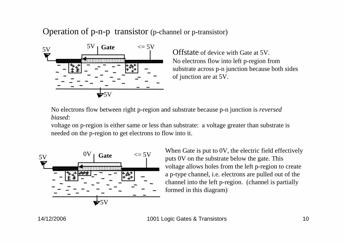
5V <= 5V5V
5V
Gate
When Gate is put to 0V, the electric field effectively puts 0V on the substrate below the gate. This voltage allows holes from the left p-region to create a p-type channel, i.e. electrons are pulled out of the channel into the left p-region. (channel is partially formed in this diagram)
Offstateof device with Gate at 5V. No electrons flow into left p-region from substrate across p-n junction because both sides of junction are at 5V.
No electrons flow between right p-region and substrate because p-n junction is reversed biased: voltage on p-region is either same or less than substrate: a voltage greater than substrate is needed on the p-region to get electrons to flow into it.
Operation of p-n-p transistor (p-channel or p-transistor)
0V <= 5V5V
5V
Gate
14/12/2006 1001 Logic Gates & Transistors 11
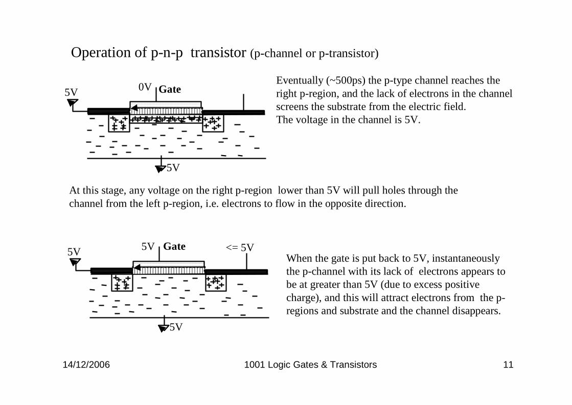
At this stage, any voltage on the right p-region lower than 5V will pull holes through the channel from the left p-region, i.e. electrons to flow in the opposite direction.
0V5V
5V
Gate
Operation of p-n-p transistor (p-channel or p-transistor)
Eventually (~500ps) the p-type channel reaches the right p-region, and the lack of electrons in the channel screens the substrate from the electric field. The voltage in the channel is 5V.
When the gate is put back to 5V, instantaneously the p-channel with its lack of electrons appears to be at greater than 5V (due to excess positive charge), and this will attract electrons from the p-regions and substrate and the channel disappears.
5V <= 5V5V
5V
Gate
14/12/2006 1001 Logic Gates & Transistors 12
Input
5V
0V
Output
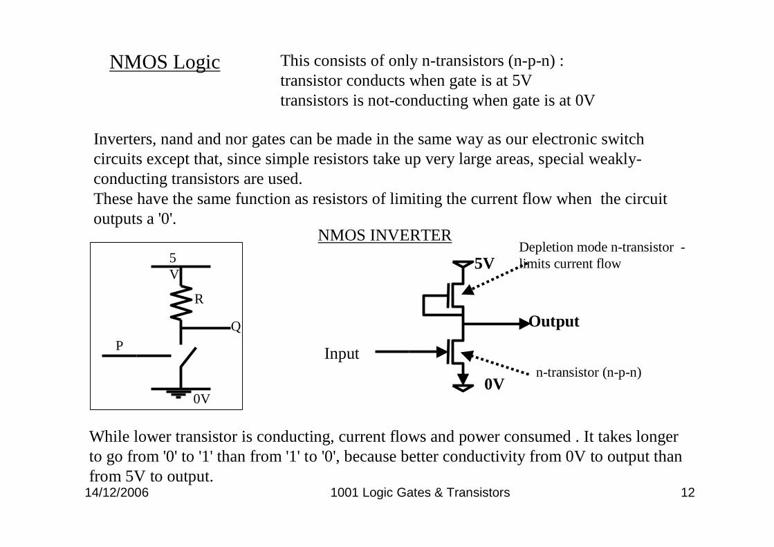
Inverters, nand and nor gates can be made in the same way as our electronic switch circuits except that, since simple resistors take up very large areas, special weakly-conducting transistors are used. These have the same function as resistors of limiting the current flow when the circuit outputs a '0'.
NMOS Logic This consists of only n-transistors (n-p-n) :transistor conducts when gate is at 5Vtransistors is not-conducting when gate is at 0V
NMOS INVERTER
n-transistor (n-p-n)
Depletion mode n-transistor -limits current flow
While lower transistor is conducting, current flows and power consumed . It takes longer to go from '0' to '1' than from '1' to '0', because better conductivity from 0V to output than from 5V to output.
P
R
Q
0V
5V
14/12/2006 1001 Logic Gates & Transistors 13
B
5V
0V
A C
R
R
H
5V
0V0V 0V
E FD
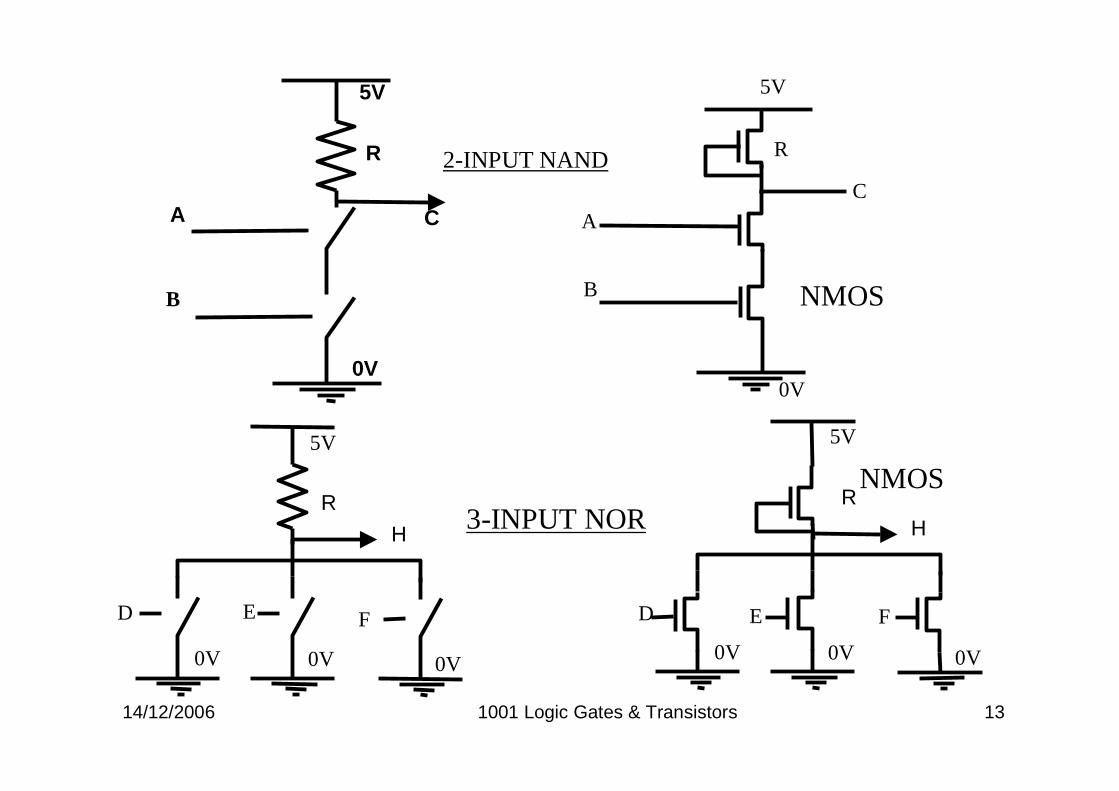
2-INPUT NAND
3-INPUT NOR
5V
C
B
A
0V
R
NMOS
R
H
5V
0V0V 0V
E FD
NMOS
14/12/2006 1001 Logic Gates & Transistors 14
Inverter 5V
0V
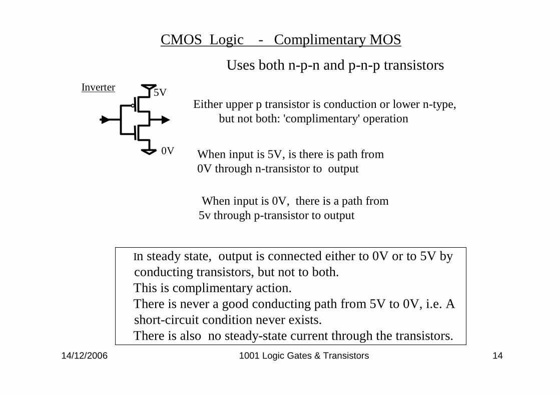
CMOS Logic - Complimentary MOS
Either upper p transistor is conduction or lower n-type, but not both: 'complimentary' operation
When input is 5V, is there is path from 0V through n-transistor to output
When input is 0V, there is a path from 5v through p-transistor to output
In steady state, output is connected either to 0V or to 5V by conducting transistors, but not to both. This is complimentary action.There is never a good conducting path from 5V to 0V, i.e. A short-circuit condition never exists.There is also no steady-state current through the transistors.
Uses both n-p-n and p-n-p transistors
14/12/2006 1001 Logic Gates & Transistors 15
Inverter5V
0V
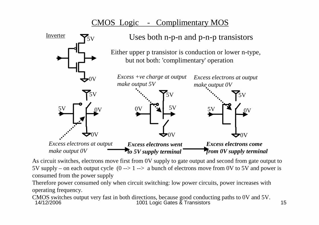
CMOS Logic - Complimentary MOS
Either upper p transistor is conduction or lower n-type, but not both: 'complimentary' operation
As circuit switches, electrons move first from 0V supply to gateoutput and second from gate output to 5V supply – on each output cycle (0 --> 1 --> a bunch of electrons move from 0V to 5V and power is consumed from the power supplyTherefore power consumed only when circuit switching: low power circuits, power increases with operating frequency.CMOS switches output very fast in both directions, because good conducting paths to 0V and 5V.
Uses both n-p-n and p-n-p transistors
5V
0V
5V 0V
Excess electrons at output make output 0V
5V
0V
0V 5V
Excess +ve charge at output make output 5V
Excess electrons went to 5V supply terminal
5V
0V
5V 0V
Excess electrons at output make output 0V
Excess electrons come from 0V supply terminal
14/12/2006 1001 Logic Gates & Transistors 16
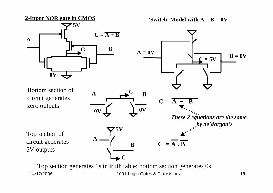
C = A + B
C BA
0V0V
AB
5V
C
2-Input NOR gate in CMOS
C = A + B
5V
BC
A
0V
'Switch' Model with A = B = 0V
A = 0VB = 0VC = 5V
Bottom section ofcircuit generateszero outputs
Top section ofcircuit generates5V outputs
C = A . B
These 2 equations are the same by deMorgan's
Top section generates 1s in truth table; bottom section generates 0s
14/12/2006 1001 Logic Gates & Transistors 17
A
A
B
B
0V
5V
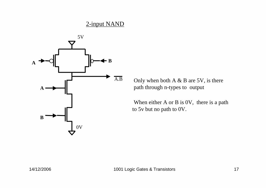
A.B Only when both A & B are 5V, is there path through n-types to output
When either A or B is 0V, there is a path to 5v but no path to 0V.
2-input NAND
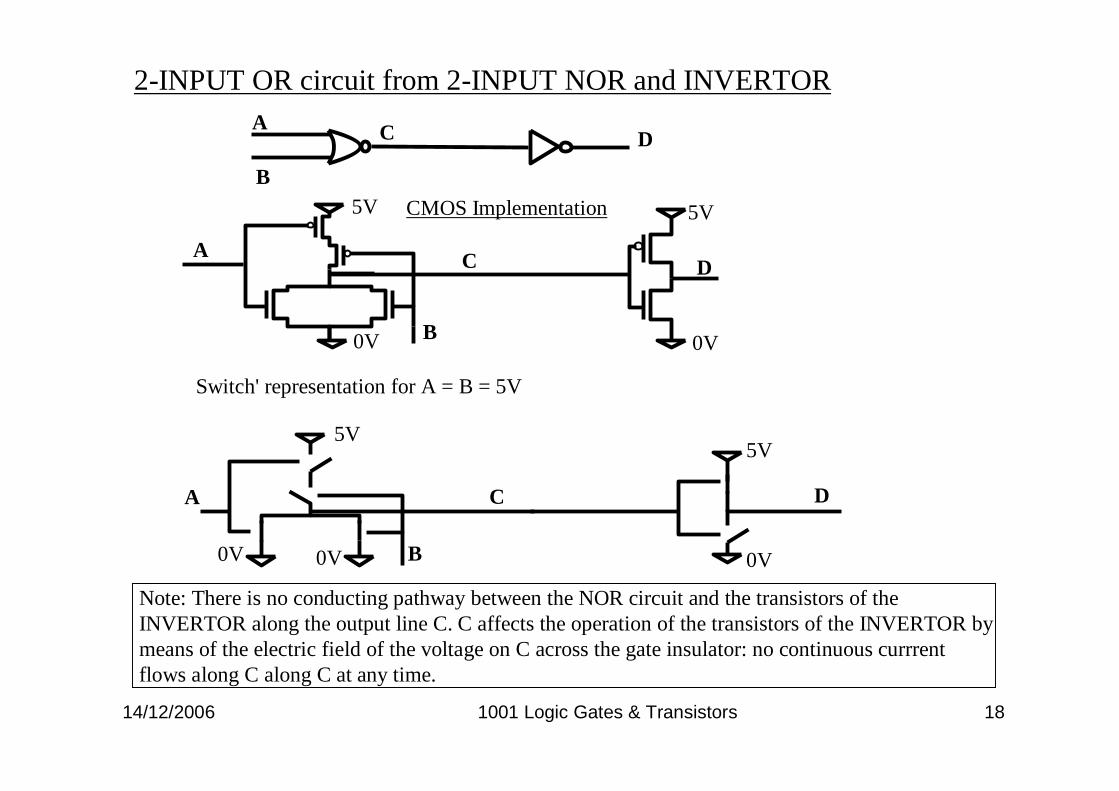
14/12/2006 1001 Logic Gates & Transistors 18
B
A C D
Switch' representation for A = B = 5V
5V5V
0V0V 0V B
C DA
2-INPUT OR circuit from 2-INPUT NOR and INVERTOR
CMOS Implementation5V 5V
0V0V
C DA
B
Note: There is no conducting pathway between the NOR circuit and the transistors of the INVERTOR along the output line C. C affects the operation of the transistors of the INVERTOR by means of the electric field of the voltage on C across the gate insulator: no continuouscurrrentflows along C along C at any time.
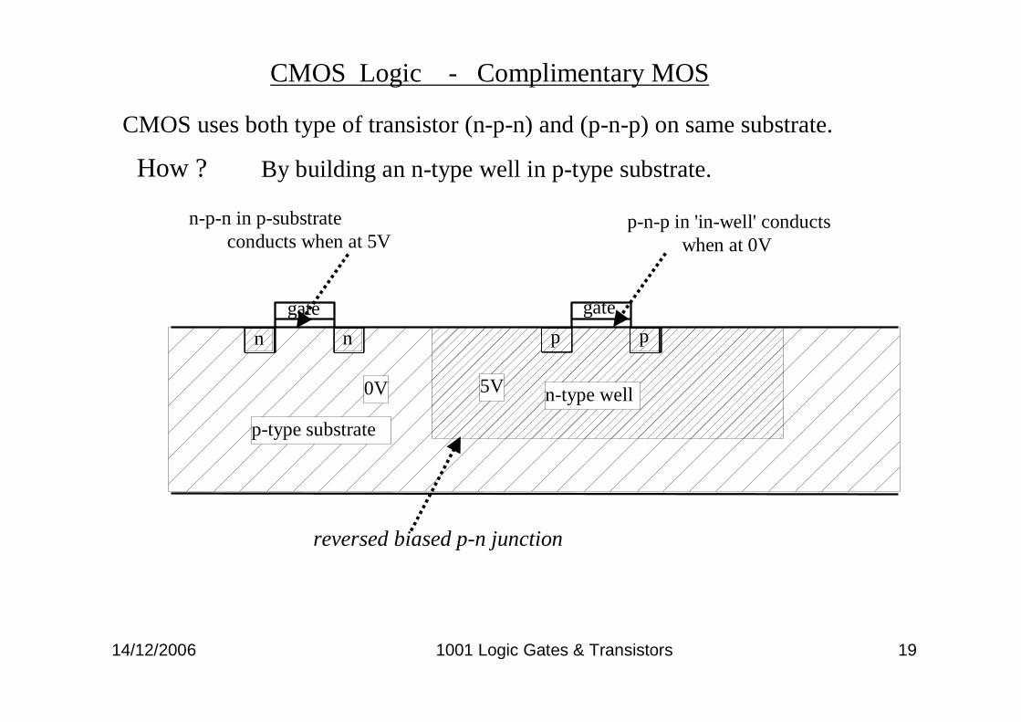
14/12/2006 1001 Logic Gates & Transistors 19
n-type well
p-type substrate
p pnn
n-p-n in p-substrate conducts when at 5V
p-n-p in 'in-well' conducts when at 0V
5V
gategate
0V
reversed biased p-n junction
CMOS Logic - Complimentary MOS
CMOS uses both type of transistor (n-p-n) and (p-n-p) on same substrate.
How ? By building an n-type well in p-type substrate.
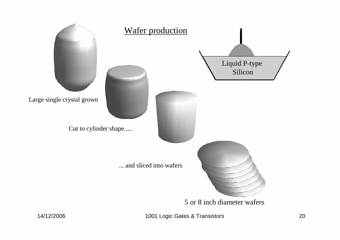
14/12/2006 1001 Logic Gates & Transistors 20
Liquid P-typeSilicon
Wafer production
Large single crystal grown
Cut to cylinder shape.....
5 or 8 inch diameter wafers
... and sliced into wafers
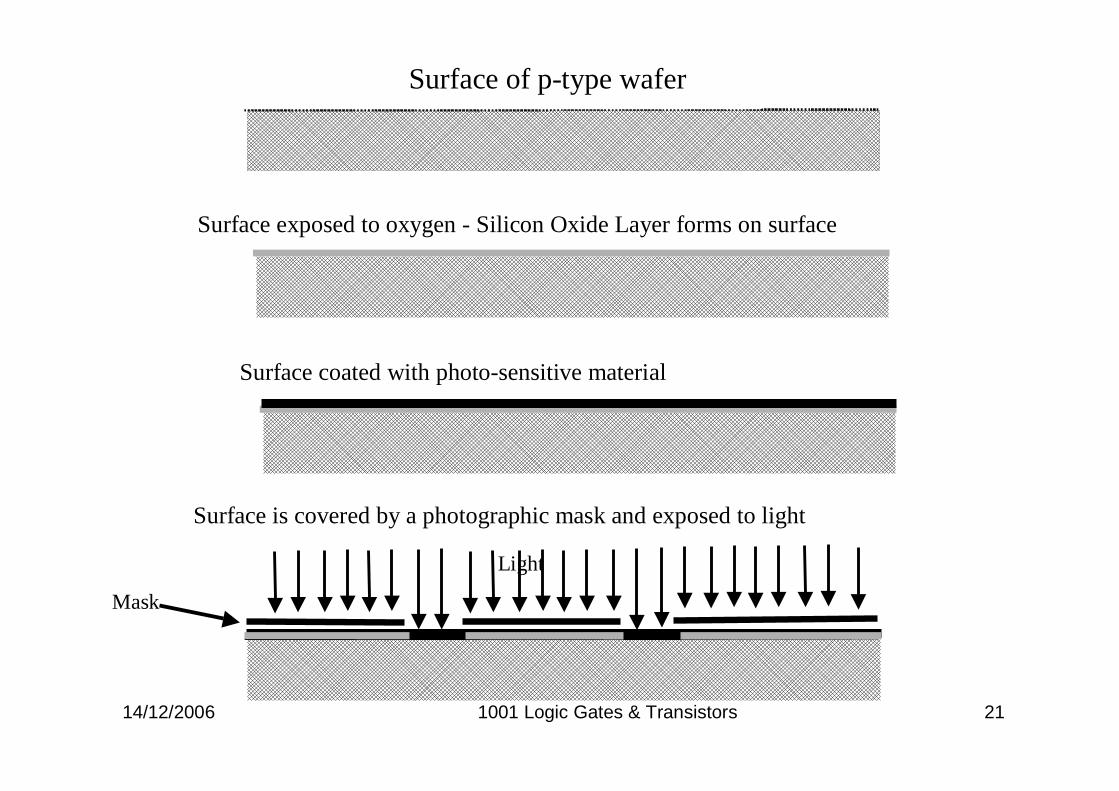
14/12/2006 1001 Logic Gates & Transistors 21
Surface exposed to oxygen - Silicon Oxide Layer forms on surface
Mask
Surface is covered by a photographic mask and exposed to light
Surface coated with photo-sensitive material
Light
Surface of p-type wafer
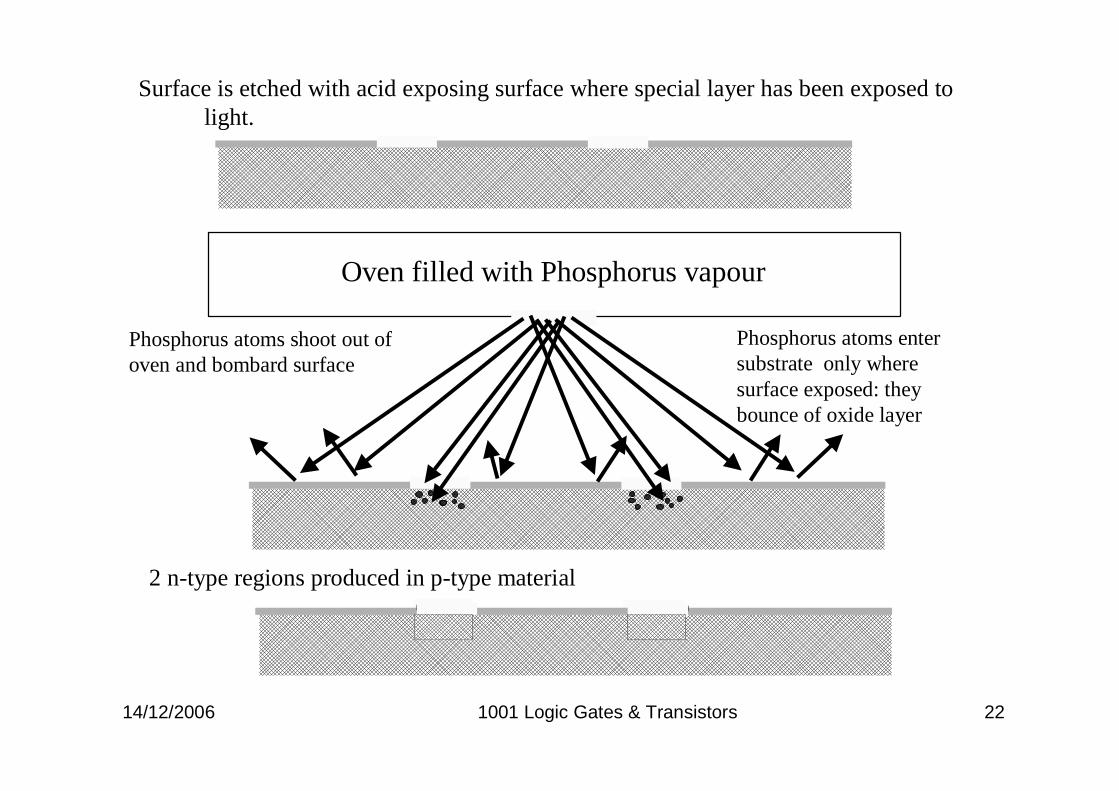
14/12/2006 1001 Logic Gates & Transistors 22
2 n-type regions produced in p-type material
Surface is etched with acid exposing surface where special layer has been exposed to light.
Phosphorus atoms enter substrate only where surface exposed: they bounce of oxide layer
Phosphorus atoms shoot out of oven and bombard surface
Oven filled with Phosphorus vapour
14/12/2006 1001 Logic Gates & Transistors 23
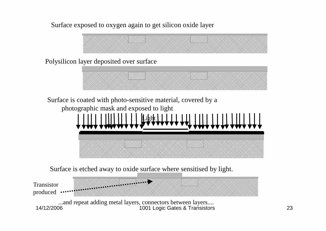
Surface exposed to oxygen again to get silicon oxide layer
Polysilicon layer deposited over surface
Surface is coated with photo-sensitive material, covered by a photographic mask and exposed to light
Light
Surface is etched away to oxide surface where sensitised by light.
Transistor produced
...and repeat adding metal layers, connectors between layers....
14/12/2006 1001 Logic Gates & Transistors 24
14/12/2006 1001 Logic Gates & Transistors 25
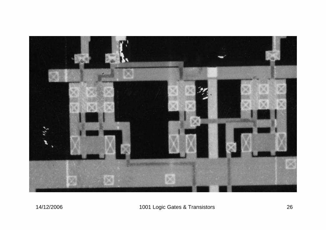
14/12/2006 1001 Logic Gates & Transistors 26
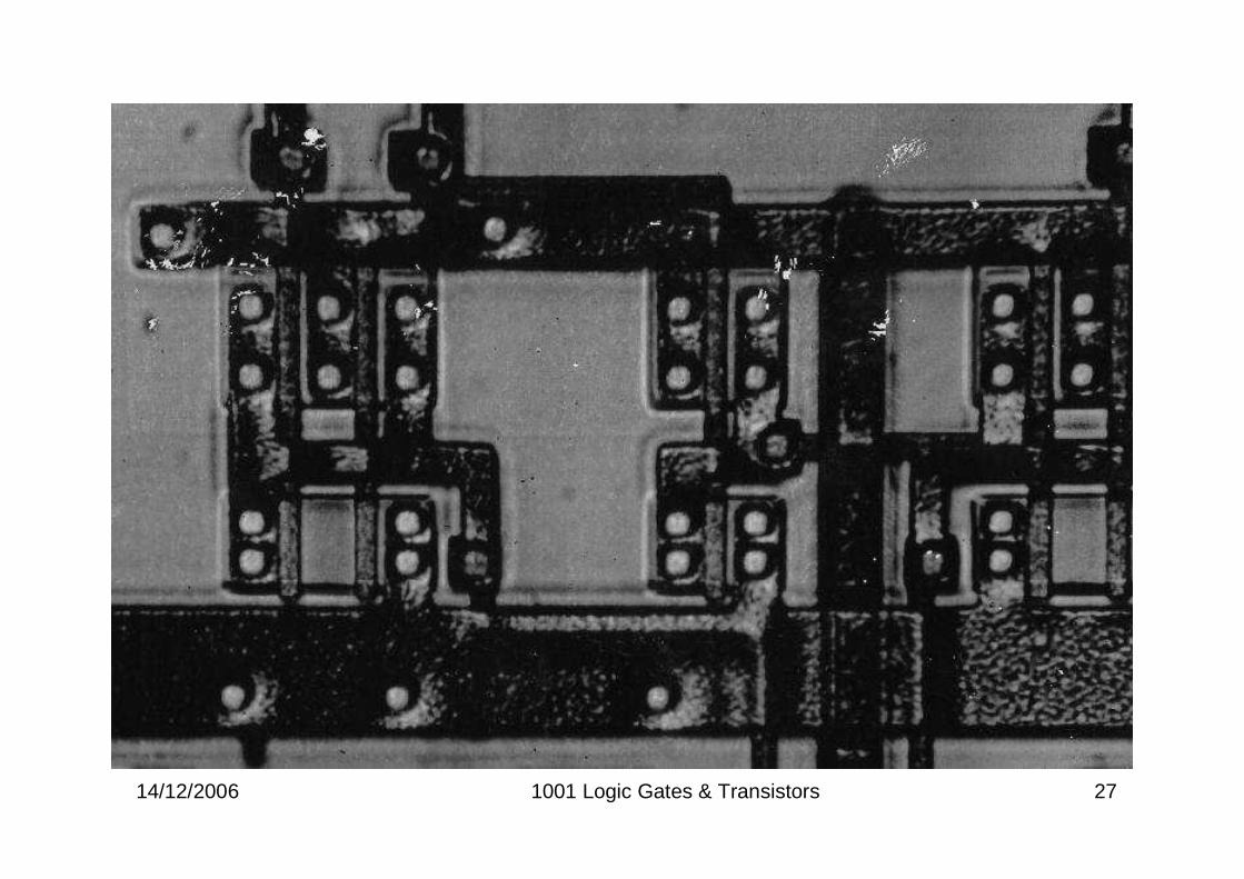
14/12/2006 1001 Logic Gates & Transistors 27
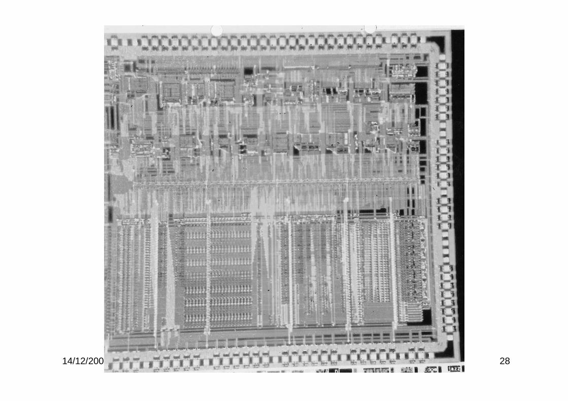
14/12/2006 1001 Logic Gates & Transistors 28
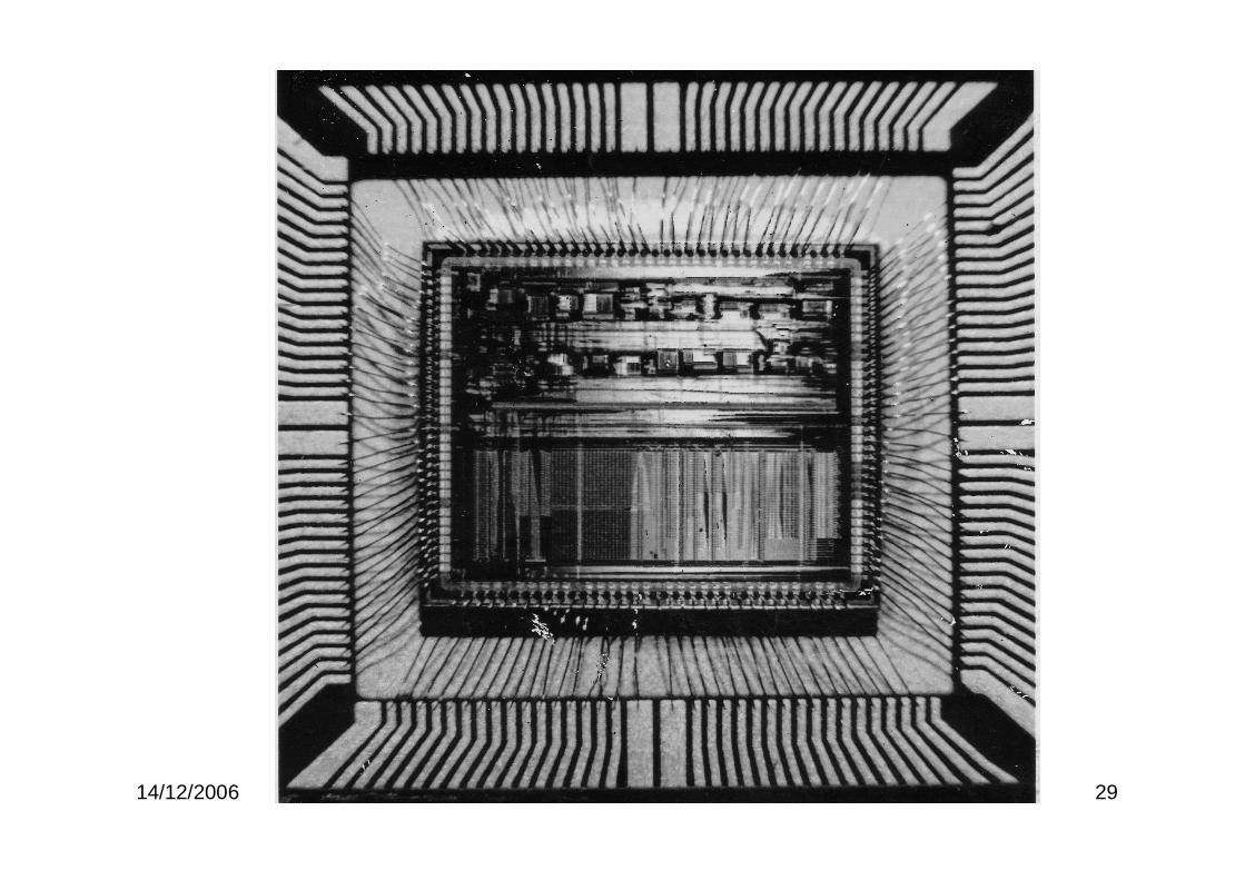
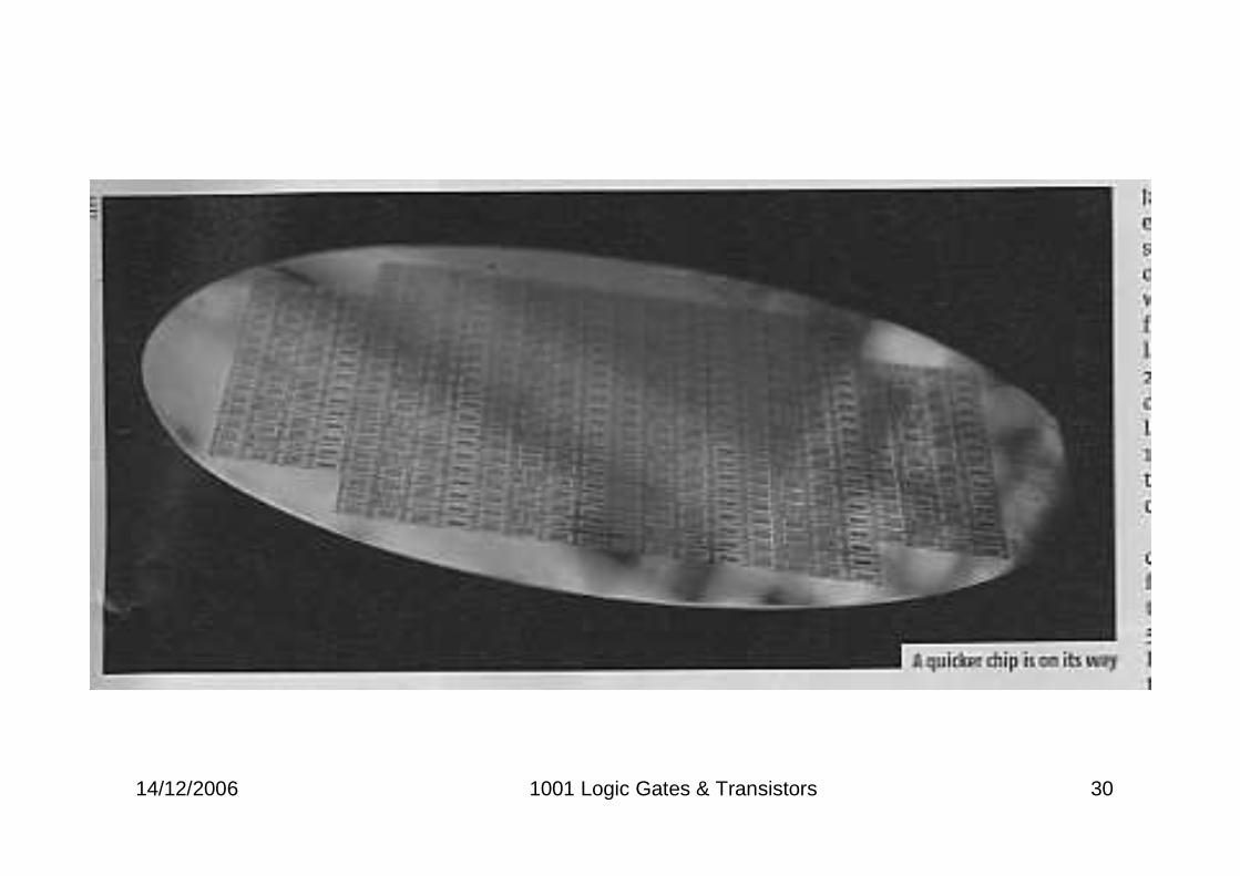
14/12/2006 1001 Logic Gates & Transistors 29
14/12/2006 1001 Logic Gates & Transistors 30
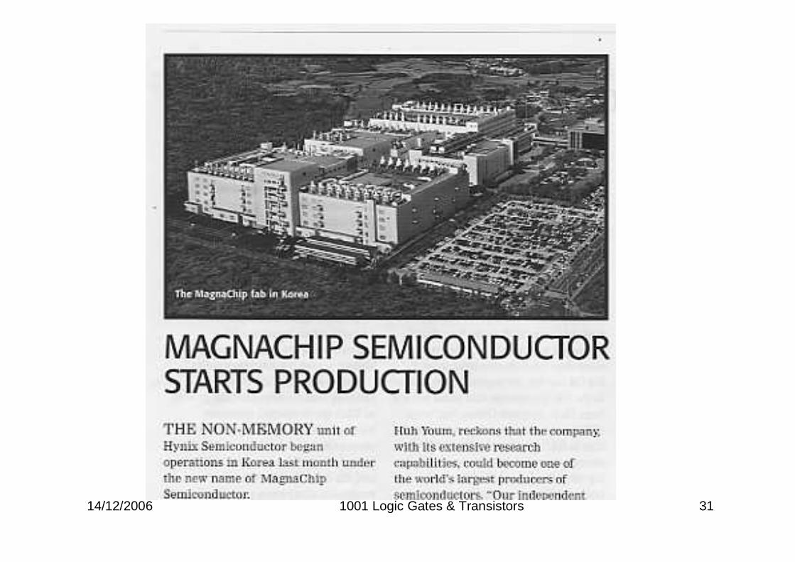
14/12/2006 1001 Logic Gates & Transistors 31


![6HPHVWHU 7LPH WDEOH ZHI -XQH $ 17 · 2020. 6. 25. · 0v /lp /3 0v 1dl +& 0gp :dqj )dqj 55 6fl 1$ 0v (ol]d /rz 0v /lp 6/ 55 (/ 1$ 0v -hqqlihu :x +rph#:: 0u -hiiuh\ &kxd 0v ,y\ 1\dp](https://img.pdfslide.us/doc/110x75/5fd5d0796b0c65670c415668/6hphvwhu-7lph-wdeoh-zhi-xqh-17-2020-6-25-0v-lp-3-0v-1dl-0gp-dqj.jpg)