Embed Size (px)
Citation preview
TPS2110A/TPS2111A
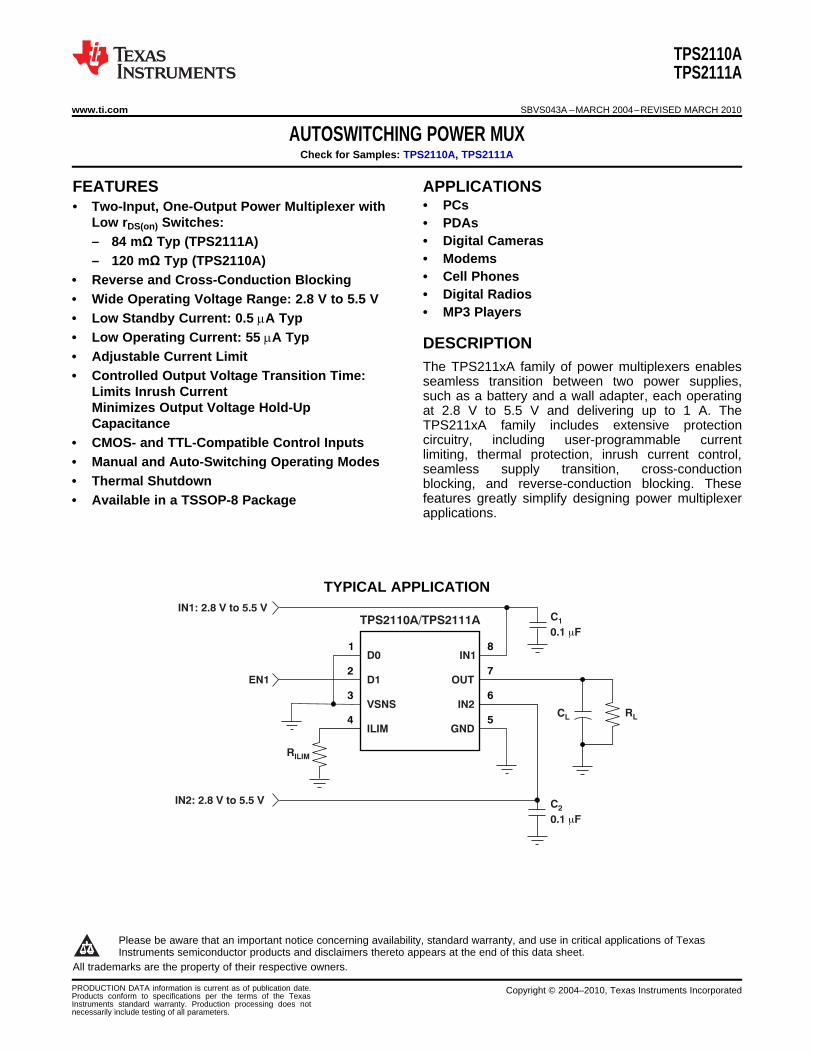
D0
D1
VSNS
ILIM
IN1
OUT
IN2
GND
8
7
6
5
1
2
3
4RL
RILIM
CL
C2
0.1 Fm
C1
0.1 Fm
EN1
IN2: 2.8 V to 5.5 V
IN1: 2.8 V to 5.5 V
TPS2110ATPS2111A
www.ti.com SBVS043A –MARCH 2004–REVISED MARCH 2010
AUTOSWITCHING POWER MUXCheck for Samples: TPS2110A, TPS2111A
1FEATURES APPLICATIONS• PCs
2• Two-Input, One-Output Power Multiplexer withLow rDS(on) Switches: • PDAs
• Digital Cameras– 84 mΩ Typ (TPS2111A)• Modems– 120 mΩ Typ (TPS2110A)• Cell Phones• Reverse and Cross-Conduction Blocking• Digital Radios• Wide Operating Voltage Range: 2.8 V to 5.5 V• MP3 Players• Low Standby Current: 0.5 mA Typ
• Low Operating Current: 55 mA Typ DESCRIPTION• Adjustable Current Limit
The TPS211xA family of power multiplexers enables• Controlled Output Voltage Transition Time: seamless transition between two power supplies,
Limits Inrush Current such as a battery and a wall adapter, each operatingMinimizes Output Voltage Hold-Up at 2.8 V to 5.5 V and delivering up to 1 A. TheCapacitance TPS211xA family includes extensive protection
circuitry, including user-programmable current• CMOS- and TTL-Compatible Control Inputslimiting, thermal protection, inrush current control,• Manual and Auto-Switching Operating Modes seamless supply transition, cross-conduction
• Thermal Shutdown blocking, and reverse-conduction blocking. Thesefeatures greatly simplify designing power multiplexer• Available in a TSSOP-8 Packageapplications.spacespacespace
space
TYPICAL APPLICATION
1
Please be aware that an important notice concerning availability, standard warranty, and use in critical applications of TexasInstruments semiconductor products and disclaimers thereto appears at the end of this data sheet.
2All trademarks are the property of their respective owners.
PRODUCTION DATA information is current as of publication date. Copyright © 2004–2010, Texas Instruments IncorporatedProducts conform to specifications per the terms of the TexasInstruments standard warranty. Production processing does notnecessarily include testing of all parameters.
TPS2110ATPS2111A
SBVS043A –MARCH 2004–REVISED MARCH 2010 www.ti.com
This integrated circuit can be damaged by ESD. Texas Instruments recommends that all integrated circuits be handled withappropriate precautions. Failure to observe proper handling and installation procedures can cause damage.
ESD damage can range from subtle performance degradation to complete device failure. Precision integrated circuits may be moresusceptible to damage because very small parametric changes could cause the device not to meet its published specifications.
AVAILABLE OPTIONSFEATURE TPS2110A TPS2111A TPS2112A TPS2113A TPS2114A TPS2115A
0.31 A to 0.63 A to 0.31 A to 0.63 A to 0.31 A to 0.63 A toCurrent Limit Adjustment Range 0.75 A 1.25 A 0.75 A 1.25 A 0.75 A 1.25 A
Manual Yes Yes No No Yes YesSwitching Modes
Automatic Yes Yes Yes Yes Yes Yes
Switch Status Output No No Yes Yes Yes Yes
ORDERING INFORMATION (1)
TA PACKAGE ORDERING NUMBER PACKAGE MARKING
TPS2110APW 2110A−40°C to 85°C TSSOP-8 (PW)
TPS2111APW 2111A
(1) For the most current package and ordering information see the Package Option Addendum at the end of this document, or see the TIweb site at www.ti.com.
ABSOLUTE MAXIMUM RATINGS (1)
Over recommended operating junction temperature range, unless otherwise noted.
TPS2110A, TPS2111A UNIT
Input voltage range at pins IN1, IN2, D0, D1, VSNS, ILIM (2) −0.3 to 6 V
Output voltage range, VO(OUT)(2) −0.3 to 6 V
TPS2110A 0.9Continuous output current, IO A
TPS2111A 1.5
Continuous total power dissipation See Dissipation Ratings table
Operating virtual junction temperature range, TJ Internally Limited
Human body model (HBM) 2 kVESD
Charged device model (CDM) 500 V
(1) Stresses beyond those listed under absolute maximum ratings may cause permanent damage to the device. These are stress ratingsonly, and functional operation of the device at these or any other conditions beyond those indicated under recommended operatingconditions is not implied. Exposure to absolute-maximum-rated conditions for extended periods may affect device reliability.
(2) All voltages are with respect to GND.
DISSIPATION RATINGSDERATING FACTOR TA ≤ 25°C POWER TA = 70°C POWER TA = 85°C POWER
PACKAGE ABOVE TA = 25°C RATING RATING RATING
TSSOP-8 (PW) 3.9 mW/°C 387 mW 213 mW 155 mW
2 Submit Documentation Feedback Copyright © 2004–2010, Texas Instruments Incorporated
Product Folder Link(s): TPS2110A TPS2111A
TPS2110ATPS2111A
www.ti.com SBVS043A –MARCH 2004–REVISED MARCH 2010
RECOMMENDED OPERATING CONDITIONSTPS2110A, TPS2111A
MIN NOM MAX UNIT
VI(IN2) ≥ 2.8 V 1.5 5.5Input voltage at IN1, VI(IN1) V
VI(IN2) < 2.8 V 2.8 5.5
VI(IN1) ≥ 2.8 V 1.5 5.5Input voltage at IN2, VI(IN2) V
VI(IN1) < 2.8 V 2.8 5.5
Input voltage: VI(DO), VI(D1), VI(VSNS) 0 5.5 V
TPS2110A 0.31 0.75Current limit adjustment range, IO(OUT) A
TPS2111A 0.63 1.25
Operating virtual junction temperature, TJ –40 125 °C
ELECTRICAL CHARACTERISTICS: Power SwitchOver recommended operating junction temperature, VI(IN1) = VI(IN2) = 5.5 V, and RILIM = 400 Ω, unless otherwise noted.
TPS2110A TPS2111A
PARAMETER TEST CONDITIONS MIN TYP MAX MIN TYP MAX UNIT
VI(IN1) = VI(IN2) = 5.0 V 120 140 84 110TJ = 25°C, VI(IN1) = VI(IN2) = 3.3 V 120 140 84 110 mΩIL = 500 mADrain-source
VI(IN1) = VI(IN2) = 2.8 V 120 140 84 110on-state rDS(on)(1)
resistance VI(IN1) = VI(IN2) = 5.0 V 220 150(INx−OUT) TJ = 125°C, VI(IN1) = VI(IN2) = 3.3 V 220 150 mΩIL = 500 mA
VI(IN1) = VI(IN2) = 2.8 V 220 150
(1) The TPS211xA can switch a voltage as low as 1.5 V as long as there is a minimum of 2.8 V at one of the input power pins. In thisspecific case, the lower supply voltage has no effect on the IN1 and IN2 switch on-resistances.
ELECTRICAL CHARACTERISTICSOver recommended operating junction temperature, VI(IN1) = VI(IN2) = 5.5 V, IO(OUT) = 0 A, and RILIM = 400 Ω, unless otherwisenoted.
TPS2110A, TPS2111A
PARAMETER TEST CONDITIONS MIN TYP MAX UNIT
LOGIC INPUTS (D0 AND D1)
High-level input voltage VIH 2 V
Low-level input voltage VIL 0.7 V
D0 or D1 = High, sink current 1Input current at D0 or D1 mA
D0 or D1 = Low, source current 0.5 1.4 5
SUPPLY AND LEAKAGE CURRENTS
D1 = High, D0 = Low (IN1 active), 55 90VI(IN2) = 3.3 V
D1 = High, D0 = Low (IN1 active), 1 12Supply current from IN1 (operating) mAVI(IN1) = 3.3 V
D0 = D1 = Low (IN2 active), VI(IN2) = 3.3 V 75
D0 = D1 = Low (IN2 active), VI(IN1) = 3.3 V 1
D1 = High, D0 = Low (IN1 active), 1VI(IN2) = 3.3 V
D1 = High, D0 = Low (IN1 active), 75Supply current from IN2 (operating) mAVI(IN1) = 3.3 V
D0 = D1 = Low (IN2 active), VI(IN2) = 3.3 V 1 12
D0 = D1 = Low (IN2 active), VI(IN1) = 3.3 V 55 90
Copyright © 2004–2010, Texas Instruments Incorporated Submit Documentation Feedback 3
Product Folder Link(s): TPS2110A TPS2111A
TPS2110ATPS2111A
SBVS043A –MARCH 2004–REVISED MARCH 2010 www.ti.com
ELECTRICAL CHARACTERISTICS (continued)Over recommended operating junction temperature, VI(IN1) = VI(IN2) = 5.5 V, IO(OUT) = 0 A, and RILIM = 400 Ω, unless otherwisenoted.
TPS2110A, TPS2111A
PARAMETER TEST CONDITIONS MIN TYP MAX UNIT
SUPPLY AND LEAKAGE CURRENTS, continued
D0 = D1 = High (inactive), VI(IN2) = 3.3 V 0.5 2Quiescent current from IN1 (standby) mA
D0 = D1 = High (inactive), VI(IN1) = 3.3 V 1
D0 = D1 = High (inactive), VI(IN2) = 3.3 V 1Quiescent current from IN2 (standby) mA
D0 = D1 = High (inactive), VI(IN1) = 3.3 V 0.5 2
Forward leakage current from IN1 D0 = D1 = High (inactive), IN2 open, VO(OUT) 0.1 5 mA(measured from OUT to GND) = 0 V (shorted), TJ = 25°C
Forward leakage current from IN2 D0 = D1 = High (inactive), IN1 open, VO(OUT) 0.1 5 mA(measured from OUT to GND) = 0 V (shorted), TJ = 25°C
Reverse leakage current to INx (measured D0 = D1 = High (inactive), VI(INx) = 0 V, 0.3 5 mAfrom INx to GND) VO(OUT) = 5.5 V, TJ = 25°C
CURRENT LIMIT CIRCUIT
RILIM = 400 Ω 0.51 0.63 0.80TPS2110A A
RILIM = 700 Ω 0.30 0.36 0.50Current limit accuracy
RILIM = 400 Ω 0.95 1.25 1.56TPS2111A A
RILIM = 700 Ω 0.47 0.71 0.99
Time for short-circuit output current to settleCurrent limit settling time td 1 mswithin 10% of its steady state value.
Input current at ILIM VI(ILIM) = 0 V, IO(OUT) = 0 A –15 0 mA
VSNS COMPARATOR
VI(VSNS) ↑ 0.78 0.80 0.82VSNS threshold voltage V
VI(VSNS) ↓ 0.735 0.755 0.775
VSNS comparator hysteresis 30 60 mV
Deglitch of VSNS comparator (both ↑ ↓ ) 90 150 220 ms
Input current 0 V ≤ VI(VSNS) ≤ 5.5 V –1 1 mA
UVLO
Falling edge 1.15 1.25IN1 and IN2 UVLO V
Rising edge 1.30 1.35
IN1 and IN2 UVLO hysteresis 30 57 65 mV
Falling edge 2.4 2.53Internal VDD UVLO V(the higher of IN1 and IN2) Rising edge 2.58 2.8
Internal VDD UVLO hysteresis 30 50 75 mV
UVLO deglitch for IN1, IN2 Falling edge 110 ms
REVERSE CONDUCTION BLOCKING
D0 = D1 = high, VI(INx) = 3.3 V. Connect OUTMinimum output-to-input to a 5-V supply through a series 1-kΩ resistor.voltage difference to block ΔVO(I_block) 80 100 120 mVLet D0 = low. Slowly decrease the supplyswitching voltage until OUT connects to IN1.
THERMAL SHUTDOWN
Thermal shutdown threshold TPS211xA is in current limit. 135 °C
Recovery from thermal shutdown TPS211xA is in current limit. 125 °C
Hysteresis 10 °C
IN2−IN1 COMPARATORS
Hysteresis of IN2−IN1 comparator 0.1 0.2 V
Deglitch of IN2−IN1 comparator (both ↑ ↓) 10 20 50 ms
4 Submit Documentation Feedback Copyright © 2004–2010, Texas Instruments Incorporated
Product Folder Link(s): TPS2110A TPS2111A
TPS2110ATPS2111A
www.ti.com SBVS043A –MARCH 2004–REVISED MARCH 2010
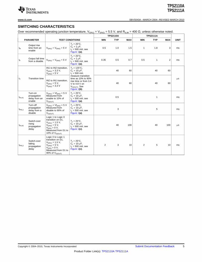
SWITCHING CHARACTERISTICSOver recommended operating junction temperature, VI(IN1) = VI(IN2) = 5.5 V, and RILIM = 400 Ω, unless otherwise noted.
TPS2110A TPS2111A
PARAMETER TEST CONDITIONS MIN TYP MAX MIN TYP MAX UNIT
TJ = 25°C,Output rise CL = 1 mF,tR time from an VI(IN1) = VI(IN2) = 5 V 0.5 1.0 1.5 1 1.8 3 msIL = 500 mA; seeenable Figure 1(a).
TJ = 25°C,Output fall time CL = 1 mF,tF VI(IN1) = VI(IN2) = 5 V 0.35 0.5 0.7 0.5 1 2 msfrom a disable IL = 500 mA; see
Figure 1(a).
IN1 to IN2 transition, TJ = 125°C,VI(IN1) = 3.3 V, CL = 10 mF, 40 60 40 60VI(IN2) = 5 V IL = 500 mA;
measure transitiontT Transition time time as 10% to 90% ms
IN2 to IN1 transition, rise time or from 3.4VI(IN1) = 5 V, 40 60 40 60V to 4.8 V onVI(IN2) = 3.3 V VO(OUT). See
Figure 1(b).
Turn-on VI(IN1) = VI(IN2) = 5 V TJ = 25°C,propagation Measured from CL = 10 mF,tPLH1 0.5 1 msdelay from an enable to 10% of IL = 500 mA; seeenable VO(OUT) Figure 1(a).
Turn-off VI(IN1) = VI(IN2) = 5 V TJ = 25°C,propagation Measured from CL = 10 mF,tPHL1 3 5 msdelay from a disable to 90% of IL = 500 mA; seedisable VO(OUT) Figure 1(a).
Logic 1 to Logic 0transition on D1,Switch-over TJ = 25°C,VI(IN1) = 1.5 V,rising CL = 10 mF,tPLH2 VI(IN2) = 5 V, 40 100 40 100 mspropagation IL = 500 mA; seeVI(D0) = 0 V,delay Figure 1(c).Measured from D1 to10% of VO(OUT)
Logic 0 to Logic 1transition on D1,Switch-over TJ = 25°C,VI(IN1) = 1.5 V,falling CL = 10 mF,tPHL2 VI(IN2) = 5 V, 2 3 10 2 5 10 mspropagation IL = 500 mA; seeVI(D0) = 0 V,delay Figure 1(c).Measured from D1 to90% of VO(OUT)
Copyright © 2004–2010, Texas Instruments Incorporated Submit Documentation Feedback 5
Product Folder Link(s): TPS2110A TPS2111A
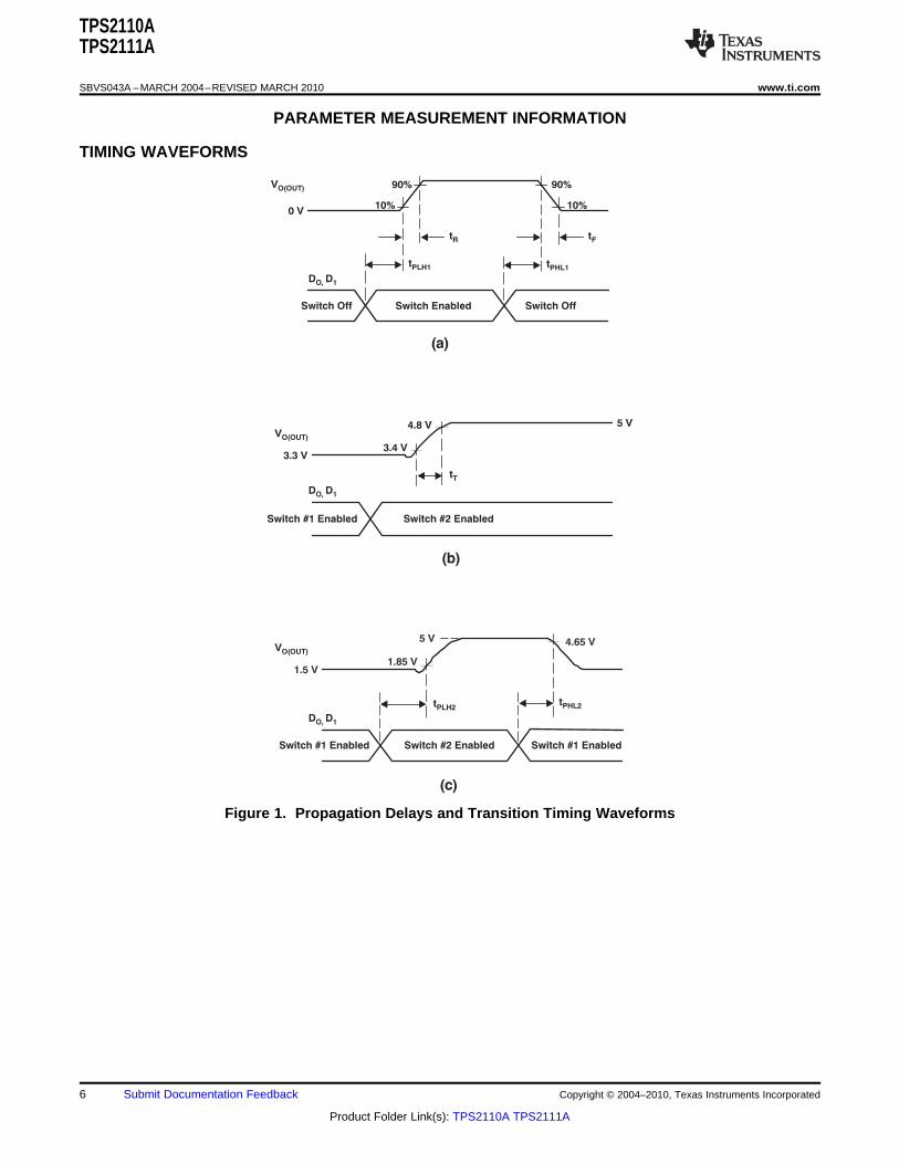
(c)
1.5 V1.85 V
4.65 V5 VVO(OUT)
tPLH2tPHL2
Switch #1 Enabled Switch #1 EnabledSwitch #2 Enabled
(b)
3.3 V
5 V4.8 V
3.4 V
VO(OUT)
tT
D DO, 1
D DO, 1
D DO, 1
Switch #1 Enabled Switch #2 Enabled
10%
90% 90%
10%
tR
VO(OUT)
tPLH1 tPHL1
tF
0 V
Switch OffSwitch Off Switch Enabled
(a)
TPS2110ATPS2111A
SBVS043A –MARCH 2004–REVISED MARCH 2010 www.ti.com
PARAMETER MEASUREMENT INFORMATION
TIMING WAVEFORMS
Figure 1. Propagation Delays and Transition Timing Waveforms
6 Submit Documentation Feedback Copyright © 2004–2010, Texas Instruments Incorporated
Product Folder Link(s): TPS2110A TPS2111A
D0
D1
VSNS
ILIM
IN1
OUT
IN2
GND
1
2
3
4
8
7
6
5
TPS2110ATPS2111A
www.ti.com SBVS043A –MARCH 2004–REVISED MARCH 2010
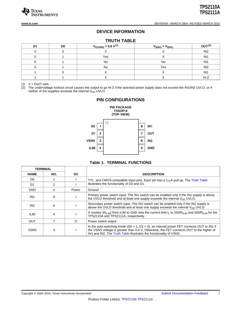
DEVICE INFORMATION
TRUTH TABLED1 D0 VI(VSNS) > 0.8 V (1) VI(IN2) > VI(IN1) OUT (2)
0 0 X X IN2
0 1 Yes X IN1
0 1 No No IN1
0 1 No Yes IN2
1 0 X X IN1
1 1 X X Hi-Z
(1) X = Don’t care.(2) The undervoltage lockout circuit causes the output to go Hi-Z if the selected power supply does not exceed the IN1/IN2 UVLO, or if
neither of the supplies exceeds the internal VDD UVLO.
PIN CONFIGURATIONS
PW PACKAGETSSOP-8
(TOP VIEW)
Table 1. TERMINAL FUNCTIONS
TERMINAL
NAME NO. I/O DESCRIPTION
D0 1 I TTL- and CMOS-compatible input pins. Each pin has a 1-mA pull-up. The Truth Tableillustrates the functionality of D0 and D1.D1 2 I
GND 5 Power Ground
Primary power switch input. The IN1 switch can be enabled only if the IN1 supply is aboveIN1 8 I the UVLO threshold and at least one supply exceeds the internal VDD UVLO.
Secondary power switch input. The IN2 switch can be enabled only if the IN2 supply isIN2 6 I above the UVLO threshold and at least one supply exceeds the internal VDD UVLO.
A resistor (RILIM) from ILIM to GND sets the current limit IL to 250/RILIM and 500/RILIM for theILIM 4 I TPS2110A and TPS2111A, respectively.
OUT 7 O Power switch output
In the auto-switching mode (D0 = 1, D1 = 0), an internal power FET connects OUT to IN1 ifVSNS 3 I the VSNS voltage is greater than 0.8 V. Otherwise, the FET connects OUT to the higher of
IN1 and IN2. The Truth Table illustrates the functionality of VSNS.
Copyright © 2004–2010, Texas Instruments Incorporated Submit Documentation Feedback 7
Product Folder Link(s): TPS2110A TPS2111A
Thermal
Sense
Charge
Pump
Q is on2 Q is on1
UVLO (V )DD
UVLO (IN2)
UVLO (IN1)
D0
D1
VI(SNS) > 0.8 V
VO(OUT) > VI(INx)
EN2 EN1
Control
Logic
+
+
100 mV
0.8 V
0.6
V
Cross-Conduction
Detector
0.5 V
k IO(OUT)´
IO(OUT)
TPS2110A: k = 0.2%
TPS2111A: k = 0.1%
IN2
UVLO
VDD
UVLO
IN1
UVLO
V = 0 Vf V = 0 Vf
1 Am
1 Am
Internal VDD
IN18
IN26
D0
D1
1
2
VSNS3
GND5
IN1
IN2
EN1
Q1
Q2
4
7OUT
ILIM
TPS2110ATPS2111A
SBVS043A –MARCH 2004–REVISED MARCH 2010 www.ti.com
FUNCTIONAL BLOCK DIAGRAM
8 Submit Documentation Feedback Copyright © 2004–2010, Texas Instruments Incorporated
Product Folder Link(s): TPS2110A TPS2111A
V
2 V/divI(D0)
V
2 V/divI(D1)
V
2 V/divO(OUT)
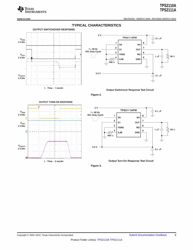
OUTPUT SWITCHOVER RESPONSE
Output Switchover Response Test Circuitt Time 1 ms/div--
TPS2111APW
D0
D1
VSNS
ILIM
IN1
OUT
IN2
GND
8
7
6
5
1
2
3
450 W
0.1 Fm
0.1 Fm
3.3 V
5 V
400 W
f = 28 Hz
78% Duty Cycle
1 Fm
V
2 V/divI(D0)
V
2 V/divI(D1)
V
2 V/divO(OUT)
OUTPUT TURN-ON RESPONSE
t Time 2 ms/div-- Output Turn-On Response Test Circuit
TPS2111APW
D0
D1
VSNS
ILIM
IN1
OUT
IN2
GND
8
7
6
5
1
2
3
450 W1 Fm
0.1 Fm
0.1 Fm
3.3 V
5 V
400 W
f = 28 Hz
78% Duty Cycle
TPS2110ATPS2111A
www.ti.com SBVS043A –MARCH 2004–REVISED MARCH 2010
TYPICAL CHARACTERISTICS
Figure 2.
Figure 3.
Copyright © 2004–2010, Texas Instruments Incorporated Submit Documentation Feedback 9
Product Folder Link(s): TPS2110A TPS2111A
V
2 V/divI(D0)
V
2 V/divI(D1)
V
2 V/divO(OUT)
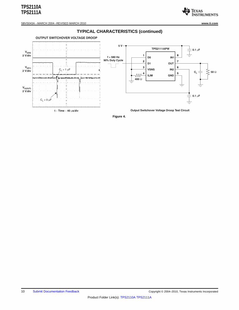
Output Switchover Voltage Droop Test Circuitt Time 40 s/div- m-
TPS2111APW
D0
D1
VSNS
ILIM
IN1
OUT
IN2
GND
8
7
6
5
1
2
3
450 W
0.1 Fm
0.1 Fm
5 V
400 W
f = 580 Hz
90% Duty Cycle
CL
OUTPUT SWITCHOVER VOLTAGE DROOP
CL
= 0 Fm
CL
= 1 Fm
TPS2110ATPS2111A
SBVS043A –MARCH 2004–REVISED MARCH 2010 www.ti.com
TYPICAL CHARACTERISTICS (continued)
Figure 4.
10 Submit Documentation Feedback Copyright © 2004–2010, Texas Instruments Incorporated
Product Folder Link(s): TPS2110A TPS2111A
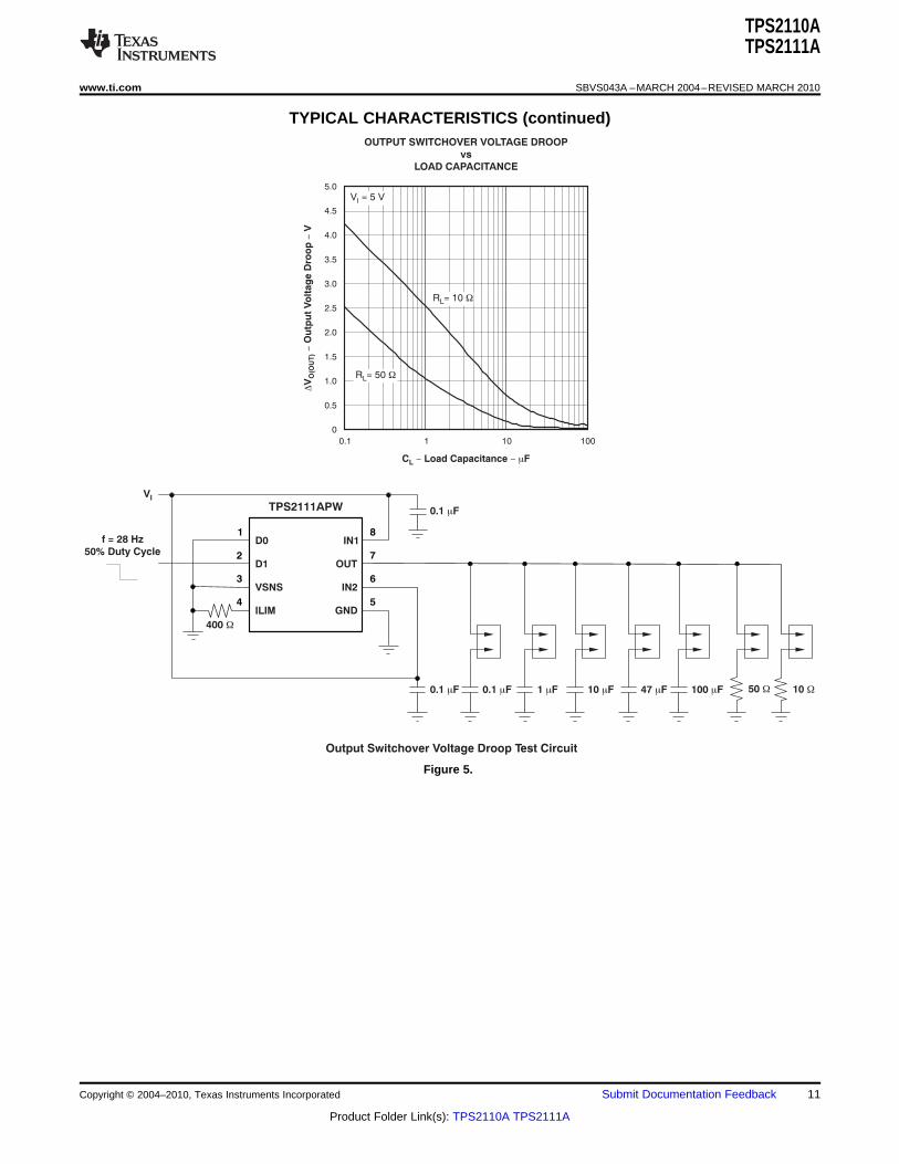
Output Switchover Voltage Droop Test Circuit
OUTPUT SWITCHOVER VOLTAGE DROOP
vs
LOAD CAPACITANCE
5.0
4.5
4.0
3.5
3.0
2.5
2.0
1.5
1.0
0.5
0
D-
VO
(OU
T)
Ou
tpu
t V
olt
ag
e D
roo
pV
-
0.1 1 10 100
C Load Capacitance F- - mL
VI= 5 V
RL= 10 W
RL= 50 W
TPS2111APW
D0
D1
VSNS
ILIM
IN1
OUT
IN2
GND
8
7
6
5
1
2
3
4
50 W 10 W0.1 Fm
0.1 Fm
VI
400 W
f = 28 Hz
50% Duty Cycle
0.1 Fm 1 Fm 10 Fm 47 Fm 100 Fm
TPS2110ATPS2111A
www.ti.com SBVS043A –MARCH 2004–REVISED MARCH 2010
TYPICAL CHARACTERISTICS (continued)
Figure 5.
Copyright © 2004–2010, Texas Instruments Incorporated Submit Documentation Feedback 11
Product Folder Link(s): TPS2110A TPS2111A
V
2 V/divI(IN1)
V
2 V/divO(OUT)
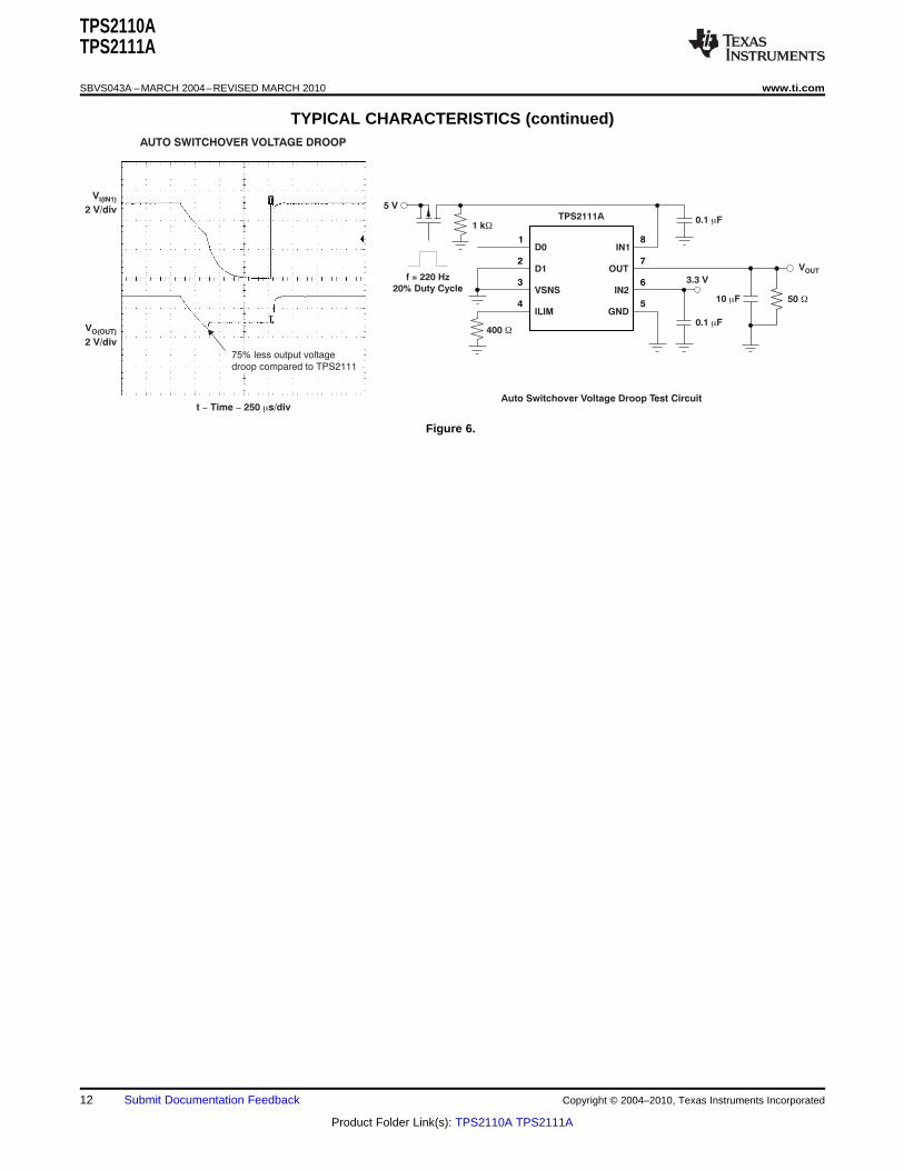
Auto Switchover Voltage Droop Test Circuitt Time 250 s/div- m-
AUTO SWITCHOVER VOLTAGE DROOP
75% less output voltage
droop compared to TPS2111
TPS2111A
D0
D1
VSNS
ILIM
IN1
OUT
IN2
GND
8
7
6
5
1
2
3
450 W
0.1 Fm
0.1 Fm
5 V
400 W
1 kW
f = 220 Hz
20% Duty Cycle10 Fm
3.3 V
VOUT
TPS2110ATPS2111A
SBVS043A –MARCH 2004–REVISED MARCH 2010 www.ti.com
TYPICAL CHARACTERISTICS (continued)
Figure 6.
12 Submit Documentation Feedback Copyright © 2004–2010, Texas Instruments Incorporated
Product Folder Link(s): TPS2110A TPS2111A
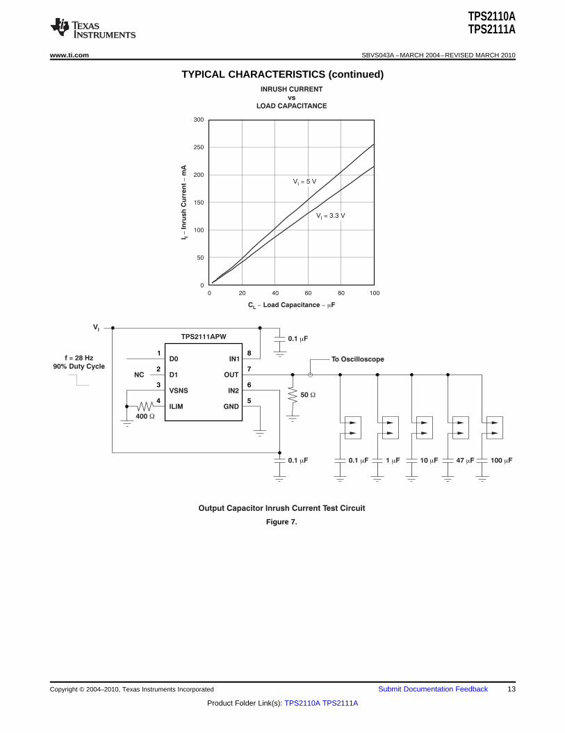
INRUSH CURRENT
vs
LOAD CAPACITANCE
300
250
200
150
100
50
0
0 40 80 100
C Load Capacitance F- - mL
VI= 5 V
VI= 3.3 V
20 60
IIn
rus
h C
urr
en
tm
A-
-I
Output Capacitor Inrush Current Test Circuit
TPS2111APW
D0
D1
VSNS
ILIM
IN1
OUT
IN2
GND
8
7
6
5
1
2
3
450 W
0.1 Fm
0.1 Fm
VI
400 W
f = 28 Hz
90% Duty Cycle
0.1 Fm 1 Fm 10 Fm 47 Fm 100 Fm
NC
To Oscilloscope
TPS2110ATPS2111A
www.ti.com SBVS043A –MARCH 2004–REVISED MARCH 2010
TYPICAL CHARACTERISTICS (continued)
Figure 7.
Copyright © 2004–2010, Texas Instruments Incorporated Submit Documentation Feedback 13
Product Folder Link(s): TPS2110A TPS2111A
180
160
140
120
100
80
60
rS
wit
ch
-On
Res
ista
nc
em
-W
DS
(on
)-
-50 0 50 100 150
T Junction Temperature C- -J °
TPS2110A
TPS2111A
120
115
110
105
100
95
90
85
80r
Sw
itch
-On
Re
sis
tan
ce
m-
WD
S(o
n)
-2 3 4 5 6
V Supply Voltage V- -I(INx)
TPS2111A
TPS2110A
0.96
0.94
0.92
0.90
0.88
0.86
0.84
0.82
IIN
1 S
up
ply
Cu
rre
nt
A-
-m
I(IN
1)
2 3 4 5 6
V IN1 Supply Voltage VI(IN1) - -
Device Disabled
V = 0 V
I = 0 AI(IN2)
O(OUT)
60
58
56
54
52
50
48
46
44
42
40
IIN
1 S
up
ply
Cu
rre
nt
A-
-m
I(IN
1)
2 3 4 5 6
V Supply Voltage VI(IN1) - -
IN1 Switch is On
V = 0 V
I = 0 AI(IN2)
O(OUT)
TPS2110ATPS2111A
SBVS043A –MARCH 2004–REVISED MARCH 2010 www.ti.com
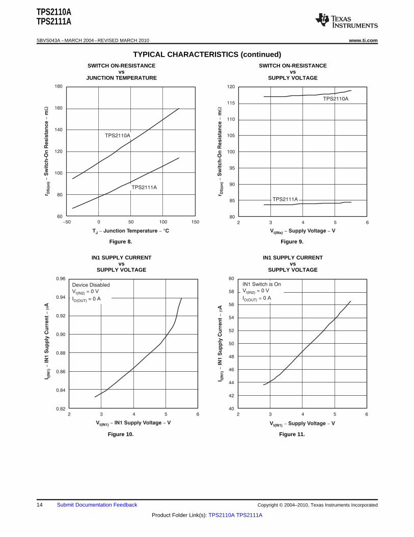
TYPICAL CHARACTERISTICS (continued)SWITCH ON-RESISTANCE SWITCH ON-RESISTANCE
vs vsJUNCTION TEMPERATURE SUPPLY VOLTAGE
Figure 8. Figure 9.
IN1 SUPPLY CURRENT IN1 SUPPLY CURRENTvs vs
SUPPLY VOLTAGE SUPPLY VOLTAGE
Figure 10. Figure 11.
14 Submit Documentation Feedback Copyright © 2004–2010, Texas Instruments Incorporated
Product Folder Link(s): TPS2110A TPS2111A

-50 0 50 100 150
T Junction Temperature C- -J °
1.2
1.0
0.8
0.6
0.4
0.2
0
IS
up
ply
Cu
rren
tA
--
mI(
INx)
Device Disabled
V = 5.5 V
V = 3.3 V
I = 0 A
I(IN1)
I(IN2)
O(OUT)
I = 3.3 VI(IN2)
I = 5.5 VI(IN1)
-50 0 50 100 150
T Junction Temperature C- -J °
IS
up
ply
Cu
rre
nt
A-
-m
I(IN
x)
IN1 Switch is On
V = 5.5 V
V = 3.3 V
I = 0 A
I(IN1)
I(IN2)
O(OUT)
II(IN2)
II(IN1)
80
70
60
50
40
30
20
10
0
TPS2110ATPS2111A
www.ti.com SBVS043A –MARCH 2004–REVISED MARCH 2010
TYPICAL CHARACTERISTICS (continued)SUPPLY CURRENT SUPPLY CURRENT
vs vsJUNCTION TEMPERATURE JUNCTION TEMPERATURE
Figure 12. Figure 13.
Copyright © 2004–2010, Texas Instruments Incorporated Submit Documentation Feedback 15
Product Folder Link(s): TPS2110A TPS2111A
TPS2110A/TPS2111A
D0
D1
VSNS
ILIM
IN1
OUT
IN2
GND
8
7
6
5
1
2
3
4RL
RILIM
CL
C2
0.1 Fm
C1
0.1 Fm
IN2: 2.8 V to 5.5 V
IN1: 2.8 V to 5.5 V
NC
R2
R1
TPS2110A/TPS2111A
D0
D1
VSNS
ILIM
IN1
OUT
IN2
GND
8
7
6
5
1
2
3
4RL
RILIM
CL
C2
0.1 Fm
C1
0.1 Fm
EN1
IN2: 2.8 V to 5.5 V
IN1: 2.8 V to 5.5 V
TPS2110ATPS2111A
SBVS043A –MARCH 2004–REVISED MARCH 2010 www.ti.com
APPLICATION INFORMATION
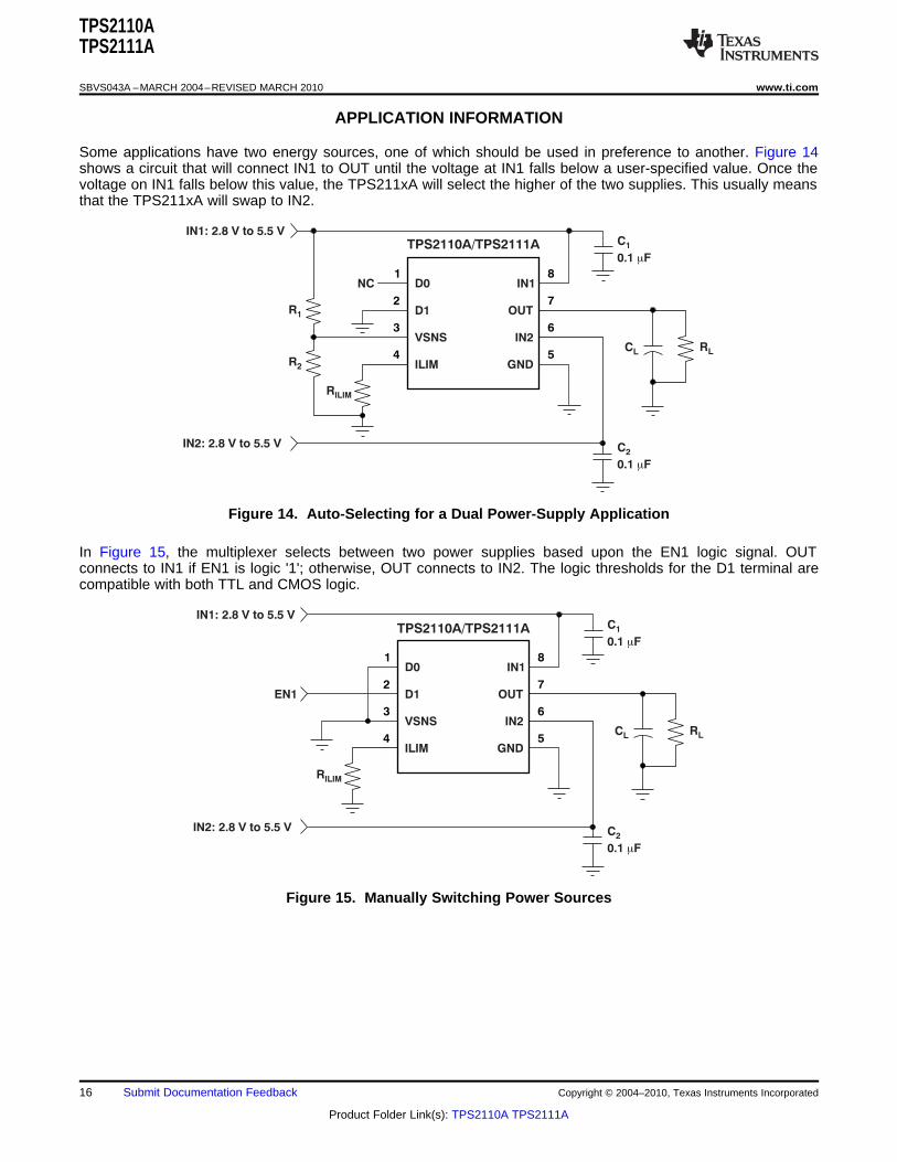
Some applications have two energy sources, one of which should be used in preference to another. Figure 14shows a circuit that will connect IN1 to OUT until the voltage at IN1 falls below a user-specified value. Once thevoltage on IN1 falls below this value, the TPS211xA will select the higher of the two supplies. This usually meansthat the TPS211xA will swap to IN2.
Figure 14. Auto-Selecting for a Dual Power-Supply Application
In Figure 15, the multiplexer selects between two power supplies based upon the EN1 logic signal. OUTconnects to IN1 if EN1 is logic '1'; otherwise, OUT connects to IN2. The logic thresholds for the D1 terminal arecompatible with both TTL and CMOS logic.
Figure 15. Manually Switching Power Sources
16 Submit Documentation Feedback Copyright © 2004–2010, Texas Instruments Incorporated
Product Folder Link(s): TPS2110A TPS2111A
TPS2110ATPS2111A
www.ti.com SBVS043A –MARCH 2004–REVISED MARCH 2010
DETAILED DESCRIPTION
AUTO-SWITCHING MODE
D0 equal to logic '1' and D1 equal to logic '0' selects the auto-switching mode. In this mode, OUT connects toIN1 if VI(VSNS) is greater than 0.8 V; otherwise, OUT connects to the higher of IN1 and IN2.
The VSNS terminal includes hysteresis equal to 3.75% to 7.5% of the threshold selected for transition from theprimary supply to the higher of the two supplies. This hysteresis helps avoid repeated switching from one supplyto the other due to resistive drops.
MANUAL SWITCHING MODE
D0 equal to logic '0' selects the manual-switching mode. In this mode, OUT connects to IN1 if D1 is equal to logic'1'; otherwise, OUT connects to IN2.
N-CHANNEL MOSFETs
Two internal high-side power MOSFETs implement a single-pole double-throw (SPDT) switch. Digital logicselects the IN1 switch, IN2 switch, or no switch (Hi-Z state). The MOSFETs have no parallel diodes sooutput-to-input current cannot flow when the FET is off. An integrated comparator prevents turn-on of a FETswitch if the output voltage is greater than the input voltage.
CROSS-CONDUCTION BLOCKING
The switching circuitry ensures that both power switches will never conduct at the same time. A comparatormonitors the gate-to-source voltage of each power FET and allows a FET to turn on only if the gate-to-sourcevoltage of the other FET is below the turn-on threshold voltage.
REVERSE-CONDUCTION BLOCKING
When the TPS211xA switches from a higher-voltage supply to a lower-voltage supply, current can potentiallyflow back from the load capacitor into the lower-voltage supply. To minimize such reverse conduction, theTPS211xA will not connect a supply to the output until the output voltage has fallen to within 100 mV of thesupply voltage. Once a supply has been connected to the output, it will remain connected regardless of outputvoltage.
CHARGE PUMP
The higher of supplies IN1 and IN2 powers the internal charge pump. The charge pump provides power to thecurrent limit amplifier and allows the output FET gate voltage to be higher than the IN1 and IN2 supply voltages.A gate voltage that is higher than the source voltage is necessary to turn on the N-channel FET.
CURRENT LIMITING
A resistor RILIM from ILIM to GND sets the current limit to 250/RILIM and 500/RILIM for the TPS2110A andTPS2111A, respectively. Setting resistor RILIM equal to zero is not recommended as that disables current limiting.
OUTPUT VOLTAGE SLEW-RATE CONTROL
The TPS211xA slews the output voltage at a slow rate when OUT switches to IN1 or IN2 from the Hi-Z state (seethe Truth Table). A slow slew rate limits the inrush current into the load capacitor. High inrush currents can glitchthe voltage bus and cause a system to hang up or reset. It can also cause reliability issues—like pit theconnector power contacts, when hot-plugging a load such as a PCI card. The TPS211xA slews the outputvoltage at a much faster rate when OUT switches between IN1 and IN2. The fast rate minimizes the outputvoltage droop and reduces the output voltage hold-up capacitance requirement.
Copyright © 2004–2010, Texas Instruments Incorporated Submit Documentation Feedback 17
Product Folder Link(s): TPS2110A TPS2111A
TPS2110ATPS2111A
SBVS043A –MARCH 2004–REVISED MARCH 2010 www.ti.com
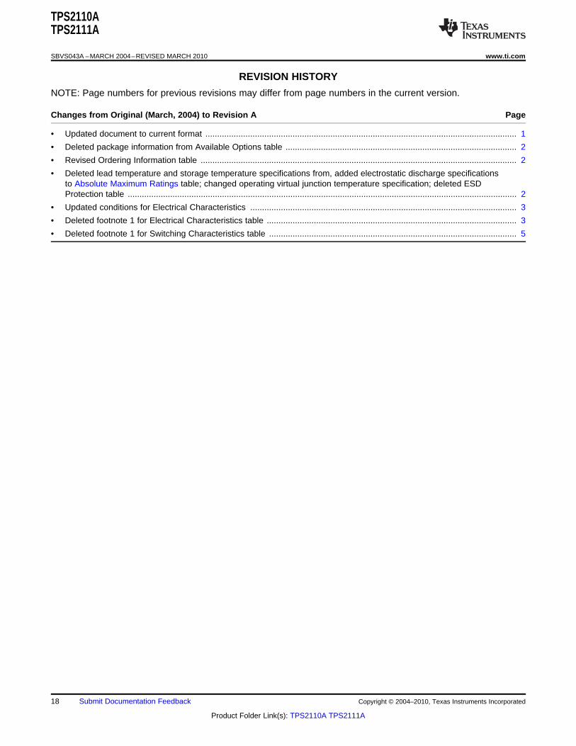
REVISION HISTORY
NOTE: Page numbers for previous revisions may differ from page numbers in the current version.
Changes from Original (March, 2004) to Revision A Page
• Updated document to current format .................................................................................................................................... 1
• Deleted package information from Available Options table .................................................................................................. 2
• Revised Ordering Information table ...................................................................................................................................... 2
• Deleted lead temperature and storage temperature specifications from, added electrostatic discharge specificationsto Absolute Maximum Ratings table; changed operating virtual junction temperature specification; deleted ESDProtection table ..................................................................................................................................................................... 2
• Updated conditions for Electrical Characteristics ................................................................................................................. 3
• Deleted footnote 1 for Electrical Characteristics table .......................................................................................................... 3
• Deleted footnote 1 for Switching Characteristics table ......................................................................................................... 5
18 Submit Documentation Feedback Copyright © 2004–2010, Texas Instruments Incorporated
Product Folder Link(s): TPS2110A TPS2111A
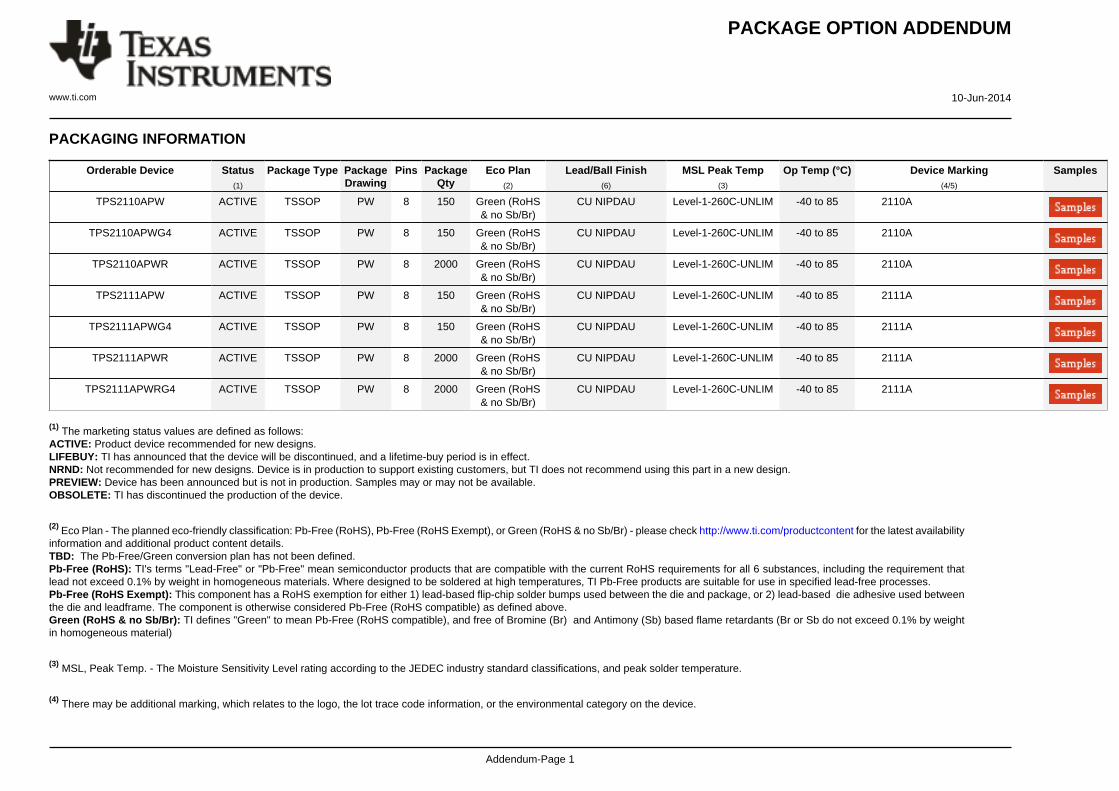
PACKAGE OPTION ADDENDUM
www.ti.com 10-Jun-2014
Addendum-Page 1
PACKAGING INFORMATION
Orderable Device Status(1)
Package Type PackageDrawing
Pins PackageQty
Eco Plan(2)
Lead/Ball Finish(6)
MSL Peak Temp(3)
Op Temp (°C) Device Marking(4/5)
Samples
TPS2110APW ACTIVE TSSOP PW 8 150 Green (RoHS& no Sb/Br)
CU NIPDAU Level-1-260C-UNLIM -40 to 85 2110A
TPS2110APWG4 ACTIVE TSSOP PW 8 150 Green (RoHS& no Sb/Br)
CU NIPDAU Level-1-260C-UNLIM -40 to 85 2110A
TPS2110APWR ACTIVE TSSOP PW 8 2000 Green (RoHS& no Sb/Br)
CU NIPDAU Level-1-260C-UNLIM -40 to 85 2110A
TPS2111APW ACTIVE TSSOP PW 8 150 Green (RoHS& no Sb/Br)
CU NIPDAU Level-1-260C-UNLIM -40 to 85 2111A
TPS2111APWG4 ACTIVE TSSOP PW 8 150 Green (RoHS& no Sb/Br)
CU NIPDAU Level-1-260C-UNLIM -40 to 85 2111A
TPS2111APWR ACTIVE TSSOP PW 8 2000 Green (RoHS& no Sb/Br)
CU NIPDAU Level-1-260C-UNLIM -40 to 85 2111A
TPS2111APWRG4 ACTIVE TSSOP PW 8 2000 Green (RoHS& no Sb/Br)
CU NIPDAU Level-1-260C-UNLIM -40 to 85 2111A
(1) The marketing status values are defined as follows:ACTIVE: Product device recommended for new designs.LIFEBUY: TI has announced that the device will be discontinued, and a lifetime-buy period is in effect.NRND: Not recommended for new designs. Device is in production to support existing customers, but TI does not recommend using this part in a new design.PREVIEW: Device has been announced but is not in production. Samples may or may not be available.OBSOLETE: TI has discontinued the production of the device.
(2) Eco Plan - The planned eco-friendly classification: Pb-Free (RoHS), Pb-Free (RoHS Exempt), or Green (RoHS & no Sb/Br) - please check http://www.ti.com/productcontent for the latest availabilityinformation and additional product content details.TBD: The Pb-Free/Green conversion plan has not been defined.Pb-Free (RoHS): TI's terms "Lead-Free" or "Pb-Free" mean semiconductor products that are compatible with the current RoHS requirements for all 6 substances, including the requirement thatlead not exceed 0.1% by weight in homogeneous materials. Where designed to be soldered at high temperatures, TI Pb-Free products are suitable for use in specified lead-free processes.Pb-Free (RoHS Exempt): This component has a RoHS exemption for either 1) lead-based flip-chip solder bumps used between the die and package, or 2) lead-based die adhesive used betweenthe die and leadframe. The component is otherwise considered Pb-Free (RoHS compatible) as defined above.Green (RoHS & no Sb/Br): TI defines "Green" to mean Pb-Free (RoHS compatible), and free of Bromine (Br) and Antimony (Sb) based flame retardants (Br or Sb do not exceed 0.1% by weightin homogeneous material)
(3) MSL, Peak Temp. - The Moisture Sensitivity Level rating according to the JEDEC industry standard classifications, and peak solder temperature.
(4) There may be additional marking, which relates to the logo, the lot trace code information, or the environmental category on the device.

PACKAGE OPTION ADDENDUM
www.ti.com 10-Jun-2014
Addendum-Page 2
(5) Multiple Device Markings will be inside parentheses. Only one Device Marking contained in parentheses and separated by a "~" will appear on a device. If a line is indented then it is a continuationof the previous line and the two combined represent the entire Device Marking for that device.
(6) Lead/Ball Finish - Orderable Devices may have multiple material finish options. Finish options are separated by a vertical ruled line. Lead/Ball Finish values may wrap to two lines if the finishvalue exceeds the maximum column width.
Important Information and Disclaimer:The information provided on this page represents TI's knowledge and belief as of the date that it is provided. TI bases its knowledge and belief on informationprovided by third parties, and makes no representation or warranty as to the accuracy of such information. Efforts are underway to better integrate information from third parties. TI has taken andcontinues to take reasonable steps to provide representative and accurate information but may not have conducted destructive testing or chemical analysis on incoming materials and chemicals.TI and TI suppliers consider certain information to be proprietary, and thus CAS numbers and other limited information may not be available for release.
In no event shall TI's liability arising out of such information exceed the total purchase price of the TI part(s) at issue in this document sold by TI to Customer on an annual basis.
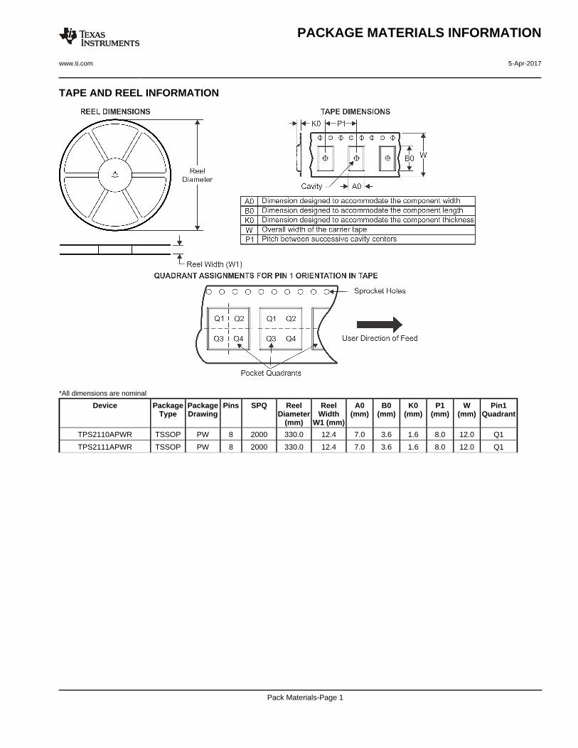
TAPE AND REEL INFORMATION
*All dimensions are nominal
Device PackageType
PackageDrawing
Pins SPQ ReelDiameter
(mm)
ReelWidth
W1 (mm)
A0(mm)
B0(mm)
K0(mm)
P1(mm)
W(mm)
Pin1Quadrant
TPS2110APWR TSSOP PW 8 2000 330.0 12.4 7.0 3.6 1.6 8.0 12.0 Q1
TPS2111APWR TSSOP PW 8 2000 330.0 12.4 7.0 3.6 1.6 8.0 12.0 Q1
PACKAGE MATERIALS INFORMATION
www.ti.com 5-Apr-2017
Pack Materials-Page 1
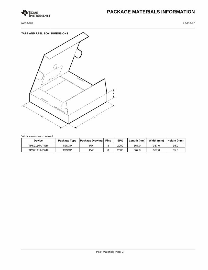
*All dimensions are nominal
Device Package Type Package Drawing Pins SPQ Length (mm) Width (mm) Height (mm)
TPS2110APWR TSSOP PW 8 2000 367.0 367.0 35.0
TPS2111APWR TSSOP PW 8 2000 367.0 367.0 35.0
PACKAGE MATERIALS INFORMATION
www.ti.com 5-Apr-2017
Pack Materials-Page 2
www.ti.com
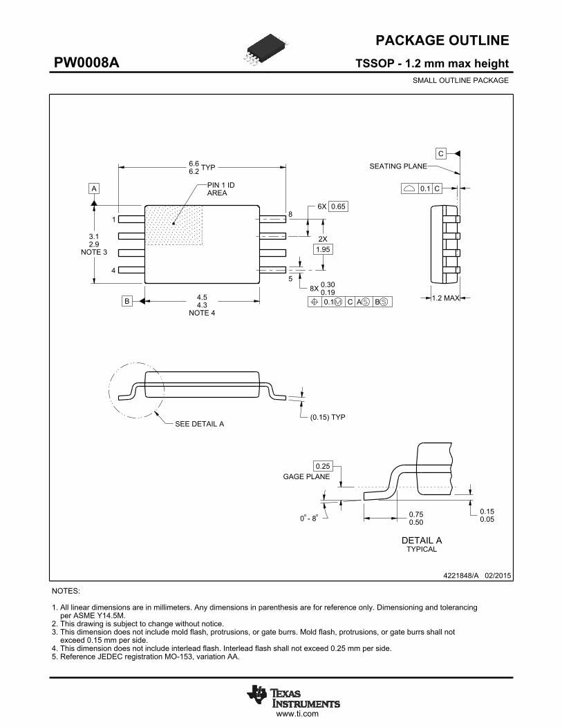
PACKAGE OUTLINE
C
TYP6.66.2
1.2 MAX
6X 0.65
8X 0.300.19
2X1.95
0.150.05
(0.15) TYP
0 - 8
0.25GAGE PLANE
0.750.50
A
NOTE 3
3.12.9
BNOTE 4
4.54.3
4221848/A 02/2015
TSSOP - 1.2 mm max heightPW0008ASMALL OUTLINE PACKAGE
NOTES: 1. All linear dimensions are in millimeters. Any dimensions in parenthesis are for reference only. Dimensioning and tolerancing per ASME Y14.5M. 2. This drawing is subject to change without notice. 3. This dimension does not include mold flash, protrusions, or gate burrs. Mold flash, protrusions, or gate burrs shall not exceed 0.15 mm per side. 4. This dimension does not include interlead flash. Interlead flash shall not exceed 0.25 mm per side.5. Reference JEDEC registration MO-153, variation AA.
18
0.1 C A B
54
PIN 1 IDAREA
SEATING PLANE
0.1 C
SEE DETAIL A
DETAIL ATYPICAL
SCALE 2.800
www.ti.com
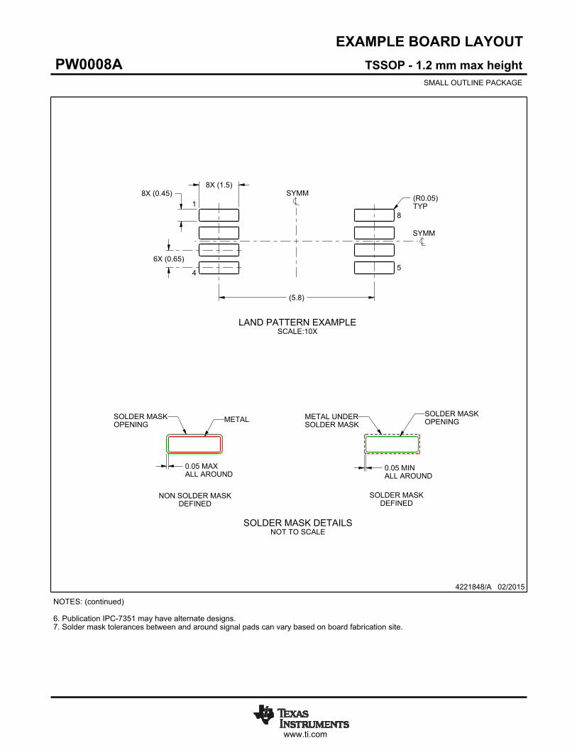
EXAMPLE BOARD LAYOUT
(5.8)
0.05 MAXALL AROUND
0.05 MINALL AROUND
8X (1.5)8X (0.45)
6X (0.65)
(R )TYP
0.05
4221848/A 02/2015
TSSOP - 1.2 mm max heightPW0008ASMALL OUTLINE PACKAGE
SYMM
SYMM
LAND PATTERN EXAMPLESCALE:10X
1
45
8
NOTES: (continued) 6. Publication IPC-7351 may have alternate designs. 7. Solder mask tolerances between and around signal pads can vary based on board fabrication site.
METALSOLDER MASKOPENING
NON SOLDER MASKDEFINED
SOLDER MASK DETAILSNOT TO SCALE
SOLDER MASKOPENING
METAL UNDERSOLDER MASK
SOLDER MASKDEFINED
www.ti.com
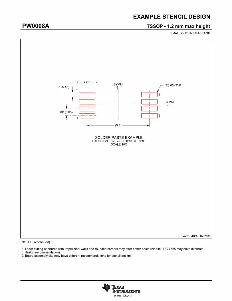
EXAMPLE STENCIL DESIGN
(5.8)
6X (0.65)
8X (0.45)8X (1.5)
(R ) TYP0.05
4221848/A 02/2015
TSSOP - 1.2 mm max heightPW0008ASMALL OUTLINE PACKAGE
NOTES: (continued) 8. Laser cutting apertures with trapezoidal walls and rounded corners may offer better paste release. IPC-7525 may have alternate design recommendations. 9. Board assembly site may have different recommendations for stencil design.
SYMM
SYMM
1
45
8
SOLDER PASTE EXAMPLEBASED ON 0.125 mm THICK STENCIL
SCALE:10X
IMPORTANT NOTICE FOR TI DESIGN INFORMATION AND RESOURCES
Texas Instruments Incorporated (‘TI”) technical, application or other design advice, services or information, including, but not limited to,reference designs and materials relating to evaluation modules, (collectively, “TI Resources”) are intended to assist designers who aredeveloping applications that incorporate TI products; by downloading, accessing or using any particular TI Resource in any way, you(individually or, if you are acting on behalf of a company, your company) agree to use it solely for this purpose and subject to the terms ofthis Notice.TI’s provision of TI Resources does not expand or otherwise alter TI’s applicable published warranties or warranty disclaimers for TIproducts, and no additional obligations or liabilities arise from TI providing such TI Resources. TI reserves the right to make corrections,enhancements, improvements and other changes to its TI Resources.You understand and agree that you remain responsible for using your independent analysis, evaluation and judgment in designing yourapplications and that you have full and exclusive responsibility to assure the safety of your applications and compliance of your applications(and of all TI products used in or for your applications) with all applicable regulations, laws and other applicable requirements. Yourepresent that, with respect to your applications, you have all the necessary expertise to create and implement safeguards that (1)anticipate dangerous consequences of failures, (2) monitor failures and their consequences, and (3) lessen the likelihood of failures thatmight cause harm and take appropriate actions. You agree that prior to using or distributing any applications that include TI products, youwill thoroughly test such applications and the functionality of such TI products as used in such applications. TI has not conducted anytesting other than that specifically described in the published documentation for a particular TI Resource.You are authorized to use, copy and modify any individual TI Resource only in connection with the development of applications that includethe TI product(s) identified in such TI Resource. NO OTHER LICENSE, EXPRESS OR IMPLIED, BY ESTOPPEL OR OTHERWISE TOANY OTHER TI INTELLECTUAL PROPERTY RIGHT, AND NO LICENSE TO ANY TECHNOLOGY OR INTELLECTUAL PROPERTYRIGHT OF TI OR ANY THIRD PARTY IS GRANTED HEREIN, including but not limited to any patent right, copyright, mask work right, orother intellectual property right relating to any combination, machine, or process in which TI products or services are used. Informationregarding or referencing third-party products or services does not constitute a license to use such products or services, or a warranty orendorsement thereof. Use of TI Resources may require a license from a third party under the patents or other intellectual property of thethird party, or a license from TI under the patents or other intellectual property of TI.TI RESOURCES ARE PROVIDED “AS IS” AND WITH ALL FAULTS. TI DISCLAIMS ALL OTHER WARRANTIES ORREPRESENTATIONS, EXPRESS OR IMPLIED, REGARDING TI RESOURCES OR USE THEREOF, INCLUDING BUT NOT LIMITED TOACCURACY OR COMPLETENESS, TITLE, ANY EPIDEMIC FAILURE WARRANTY AND ANY IMPLIED WARRANTIES OFMERCHANTABILITY, FITNESS FOR A PARTICULAR PURPOSE, AND NON-INFRINGEMENT OF ANY THIRD PARTY INTELLECTUALPROPERTY RIGHTS.TI SHALL NOT BE LIABLE FOR AND SHALL NOT DEFEND OR INDEMNIFY YOU AGAINST ANY CLAIM, INCLUDING BUT NOTLIMITED TO ANY INFRINGEMENT CLAIM THAT RELATES TO OR IS BASED ON ANY COMBINATION OF PRODUCTS EVEN IFDESCRIBED IN TI RESOURCES OR OTHERWISE. IN NO EVENT SHALL TI BE LIABLE FOR ANY ACTUAL, DIRECT, SPECIAL,COLLATERAL, INDIRECT, PUNITIVE, INCIDENTAL, CONSEQUENTIAL OR EXEMPLARY DAMAGES IN CONNECTION WITH ORARISING OUT OF TI RESOURCES OR USE THEREOF, AND REGARDLESS OF WHETHER TI HAS BEEN ADVISED OF THEPOSSIBILITY OF SUCH DAMAGES.You agree to fully indemnify TI and its representatives against any damages, costs, losses, and/or liabilities arising out of your non-compliance with the terms and provisions of this Notice.This Notice applies to TI Resources. Additional terms apply to the use and purchase of certain types of materials, TI products and services.These include; without limitation, TI’s standard terms for semiconductor products http://www.ti.com/sc/docs/stdterms.htm), evaluationmodules, and samples (http://www.ti.com/sc/docs/sampterms.htm).
Mailing Address: Texas Instruments, Post Office Box 655303, Dallas, Texas 75265Copyright © 2017, Texas Instruments Incorporated