Embed Size (px)
Citation preview

Automated FPGA Design, Verification and Layout
by
Ian Carlos Kuon
A thesis submitted in conformity with the requirementsfor the degree of Master of Applied Science
Graduate Department of Electrical and Computer EngineeringUniversity of Toronto
Copyright c© 2004 by Ian Carlos Kuon

Abstract
Automated FPGA Design, Verification and Layout
Ian Carlos Kuon
Master of Applied Science
Graduate Department of Electrical and Computer Engineering
University of Toronto
2004
The design and layout of Field-Programmable Gate Arrays (FPGAs) is a time-
consuming process that is currently performed manually. This work investigates two
issues faced when automating this task. First, an accurate comparison of layout area
between manually and automatically-generated layouts is performed. For the single
commercial architecture considered, this work found that the area of an automatically-
generated layout is only 36% larger than that needed for a manual layout. The second
half of this work focused on the steps needed to implement a complete FPGA using
automatic layout tools. New tools that aid the design and verification of an FPGA are
presented and an FPGA created with those tools was verified in simulation and then
sent for fabrication. This indicates that automatic layout tools can be used to design
complete FPGAs in a fraction of the time required for manual design.
ii

Acknowledgements
First I would like to thank my supervisor, Professor Jonathan Rose, for his support
throughout this work. Thanks to his integrity, enthusiasm and optimism I have learnt a
great deal and not just about FPGAs.
My work would not have gotten far were it not for the significant contributions of
those who started and continue to work on the GILES project. I therefore owe thanks
to Ketan Padalia, Ryan Fung and Mark Bourgeault for developing the infrastructure
I needed for my work. Aaron Egier’s concurrent work on the GILES project was also
crucial and achieving my goal of making a chip would not have been possible without
him – so thanks!
I am grateful to NSERC for financially supporting me and to the Canadian Micro-
electronics Corporation (CMC) for providing access to the technology on which my work
depends. I also greatly appreciate the funding this project received from Altera and from
NSERC through a CRD grant.
I want to thank my parents for always believing in me and encouraging me.
Finally, to Janice, thanks for being there through the ups and downs. You make me
a more complete person and remind me that there is life outside of school.
iii

Contents
List of Tables vi
List of Figures vii
List of Acronyms ix
1 Introduction 11.1 Motivation . . . . . . . . . . . . . . . . . . . . . . . . . . . . . . . . . . . 11.2 Objectives . . . . . . . . . . . . . . . . . . . . . . . . . . . . . . . . . . . 2
1.2.1 Measuring Layout Quality . . . . . . . . . . . . . . . . . . . . . . 21.2.2 Demonstrating Feasibility of Automated Design . . . . . . . . . . 3
1.3 Organization . . . . . . . . . . . . . . . . . . . . . . . . . . . . . . . . . 3
2 Background 52.1 Introduction . . . . . . . . . . . . . . . . . . . . . . . . . . . . . . . . . . 52.2 FPGA Structure . . . . . . . . . . . . . . . . . . . . . . . . . . . . . . . 52.3 FPGA Layout . . . . . . . . . . . . . . . . . . . . . . . . . . . . . . . . . 72.4 The VPR FPGA Placement and Routing System . . . . . . . . . . . . . 10
2.4.1 VPR Architecture Generation . . . . . . . . . . . . . . . . . . . . 102.4.2 VPR Placer and Router . . . . . . . . . . . . . . . . . . . . . . . 12
2.5 GILES FPGA Circuit Generation and Layout Tools . . . . . . . . . . . . 122.5.1 Netlist Generator . . . . . . . . . . . . . . . . . . . . . . . . . . . 122.5.2 Placement, Compaction and Routing . . . . . . . . . . . . . . . . 142.5.3 Previous Quality of Results using the GILES Tools . . . . . . . . 15
2.6 Alternative Automated Layout Methodologies . . . . . . . . . . . . . . . 182.6.1 Transistor-Based Methodologies . . . . . . . . . . . . . . . . . . . 182.6.2 Standard Cell Based Design . . . . . . . . . . . . . . . . . . . . . 20
3 Area Efficiency Measurement of Automated FPGA Layout 243.1 Introduction . . . . . . . . . . . . . . . . . . . . . . . . . . . . . . . . . . 243.2 Accurate Capture of Virtex-E Circuit . . . . . . . . . . . . . . . . . . . . 24
3.2.1 Virtex-E FPGA Architecture . . . . . . . . . . . . . . . . . . . . 263.2.2 Methodology . . . . . . . . . . . . . . . . . . . . . . . . . . . . . 27
3.3 Accuracy of Virtex-E Capture . . . . . . . . . . . . . . . . . . . . . . . . 303.3.1 Configuration SRAM Count Comparison . . . . . . . . . . . . . . 30
iv
3.3.2 Active Area Comparison . . . . . . . . . . . . . . . . . . . . . . . 323.4 Automated and Manual Layout Area Comparisons . . . . . . . . . . . . 32
3.4.1 General Methodology . . . . . . . . . . . . . . . . . . . . . . . . . 333.4.2 Area Result with the Original GILES Tools . . . . . . . . . . . . 353.4.3 Effect of Transistor Grouping on Area . . . . . . . . . . . . . . . 363.4.4 Effect of Cell Bloating on Area . . . . . . . . . . . . . . . . . . . 383.4.5 Effect of Metal Layer Allocation on Area . . . . . . . . . . . . . . 40
3.5 Comparison of GILES CAD Flow to Standard Cell Design . . . . . . . . 423.5.1 Methodology . . . . . . . . . . . . . . . . . . . . . . . . . . . . . 433.5.2 Comparison Qualifications/Caveats . . . . . . . . . . . . . . . . . 433.5.3 Results . . . . . . . . . . . . . . . . . . . . . . . . . . . . . . . . . 44
3.6 Summary . . . . . . . . . . . . . . . . . . . . . . . . . . . . . . . . . . . 45
4 Tools and Process for Automated Design of a Complete FPGA 474.1 Introduction . . . . . . . . . . . . . . . . . . . . . . . . . . . . . . . . . . 474.2 CAD Flow . . . . . . . . . . . . . . . . . . . . . . . . . . . . . . . . . . . 484.3 Tool Enhancements to Support Bitstream Generation . . . . . . . . . . . 49
4.3.1 T-VPack for Bitstream Generation . . . . . . . . . . . . . . . . . 494.3.2 Bitstream Generation within VPR . . . . . . . . . . . . . . . . . 50
4.4 Architecture Decisions . . . . . . . . . . . . . . . . . . . . . . . . . . . . 554.4.1 Logic Block Parameters . . . . . . . . . . . . . . . . . . . . . . . 564.4.2 Routing Structure . . . . . . . . . . . . . . . . . . . . . . . . . . . 574.4.3 Array Size . . . . . . . . . . . . . . . . . . . . . . . . . . . . . . . 574.4.4 Track Count . . . . . . . . . . . . . . . . . . . . . . . . . . . . . . 584.4.5 Connection Block Flexibility . . . . . . . . . . . . . . . . . . . . . 594.4.6 Summary of Architecture . . . . . . . . . . . . . . . . . . . . . . . 61
4.5 Periphery Design . . . . . . . . . . . . . . . . . . . . . . . . . . . . . . . 614.5.1 Periphery Generation . . . . . . . . . . . . . . . . . . . . . . . . . 644.5.2 Layout Placement and Routing Enhancements . . . . . . . . . . . 65
4.6 Configuration SRAM Programmer . . . . . . . . . . . . . . . . . . . . . . 674.6.1 Programmer Design . . . . . . . . . . . . . . . . . . . . . . . . . . 674.6.2 Power On Issues . . . . . . . . . . . . . . . . . . . . . . . . . . . 69
4.7 Bitstream Generation . . . . . . . . . . . . . . . . . . . . . . . . . . . . . 724.8 Summary . . . . . . . . . . . . . . . . . . . . . . . . . . . . . . . . . . . 74
5 Verification Methodology and Results 765.1 Introduction . . . . . . . . . . . . . . . . . . . . . . . . . . . . . . . . . . 765.2 General Verification Strategy . . . . . . . . . . . . . . . . . . . . . . . . . 775.3 Routing Resource Graph to Netlist Matching . . . . . . . . . . . . . . . . 785.4 Logical Functionality . . . . . . . . . . . . . . . . . . . . . . . . . . . . . 79
5.4.1 Methodology . . . . . . . . . . . . . . . . . . . . . . . . . . . . . 795.4.2 Test Circuits . . . . . . . . . . . . . . . . . . . . . . . . . . . . . 815.4.3 Results . . . . . . . . . . . . . . . . . . . . . . . . . . . . . . . . . 82
5.5 Electrical Functionality . . . . . . . . . . . . . . . . . . . . . . . . . . . . 835.5.1 Methodology . . . . . . . . . . . . . . . . . . . . . . . . . . . . . 83
v

5.5.2 Results . . . . . . . . . . . . . . . . . . . . . . . . . . . . . . . . . 845.5.3 Test Coverage . . . . . . . . . . . . . . . . . . . . . . . . . . . . . 84
5.6 Further Electrical Functionality Checking . . . . . . . . . . . . . . . . . . 875.7 Summary . . . . . . . . . . . . . . . . . . . . . . . . . . . . . . . . . . . 87
6 Conclusions and Future Work 886.1 Summary . . . . . . . . . . . . . . . . . . . . . . . . . . . . . . . . . . . 886.2 Contributions . . . . . . . . . . . . . . . . . . . . . . . . . . . . . . . . . 886.3 Future Work . . . . . . . . . . . . . . . . . . . . . . . . . . . . . . . . . . 89
Appendices 91
A MCNC Benchmark Circuits 91
B SRAM Programmer Verilog Description 99
Bibliography 111
vi
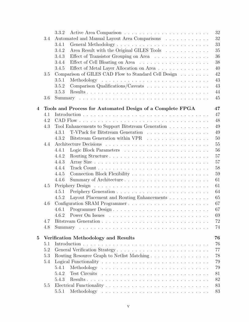
List of Tables
2.1 Area of Automated and Commercial Designs . . . . . . . . . . . . . . . . 162.2 SRAM Count of Automated and Commercial Designs . . . . . . . . . . 182.3 Comparison of Design Techniques . . . . . . . . . . . . . . . . . . . . . . 21
3.1 Comparison of Virtex-E Capture and Actual Virtex-E . . . . . . . . . . . 313.2 Effect of Metal Layer Count on Tile Area (Original Grouping) . . . . . . 363.3 Area Results with Varied Transistor Grouping . . . . . . . . . . . . . . . 373.4 Area Results with Buffered Switch Grouping . . . . . . . . . . . . . . . . 383.5 Cell Area Differences Between One and Two Metal Layer Cells . . . . . . 413.6 Active Area Differences Between One and Two Metal Layer Cells . . . . 413.7 Comparison of Routed Area of One and Two Metal Layer Cells . . . . . 413.8 Standard Cell Comparison Results . . . . . . . . . . . . . . . . . . . . . 453.9 Summary of Results Compared to Actual Virtex-E . . . . . . . . . . . . 46
4.1 Architecture Parameters . . . . . . . . . . . . . . . . . . . . . . . . . . . 63
5.1 Primary Test Circuits . . . . . . . . . . . . . . . . . . . . . . . . . . . . . 825.2 Simulation Toggle Coverage for Entire Design . . . . . . . . . . . . . . . 855.3 Simulation Toggle Coverage for Virtual Tile . . . . . . . . . . . . . . . . 85
A.1 MCNC Test Circuits Used for Architecture Experiments . . . . . . . . . 91
vii
List of Figures
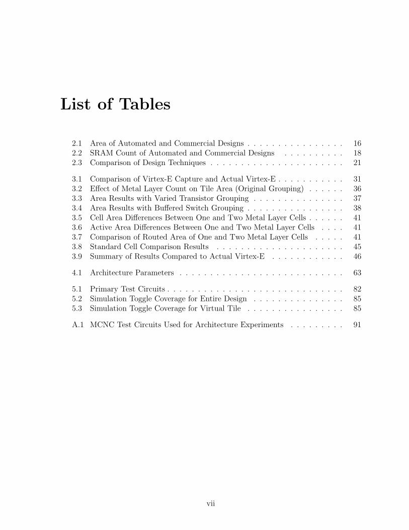
2.1 FPGA Array and Pads . . . . . . . . . . . . . . . . . . . . . . . . . . . . 62.2 Logic Cluster . . . . . . . . . . . . . . . . . . . . . . . . . . . . . . . . . 62.3 Tileable FPGA . . . . . . . . . . . . . . . . . . . . . . . . . . . . . . . . 82.4 Wire twisting to create longer tracks . . . . . . . . . . . . . . . . . . . . 92.5 VPR CAD Flow . . . . . . . . . . . . . . . . . . . . . . . . . . . . . . . . 102.6 VPR Architecture Description Language . . . . . . . . . . . . . . . . . . 112.7 GILES CAD Flow . . . . . . . . . . . . . . . . . . . . . . . . . . . . . . 132.8 Single Tile with Port Constraints . . . . . . . . . . . . . . . . . . . . . . 142.9 Standard Cell Design Style . . . . . . . . . . . . . . . . . . . . . . . . . . 20
3.1 Virtex-E Configurable Logic Block . . . . . . . . . . . . . . . . . . . . . 263.2 Logical View of Virtex-E Slice from Xilinx FPGA Editor . . . . . . . . . 283.3 Routing Track Structure . . . . . . . . . . . . . . . . . . . . . . . . . . . 293.4 Experimental CAD Flow for Area Measurements . . . . . . . . . . . . . . 333.5 Cell Bloating with Six Layers of Metal . . . . . . . . . . . . . . . . . . . 393.6 Effect of Metal Layer Count on Tile Area (Single Metal Cells) . . . . . . 42
4.1 CAD Flow . . . . . . . . . . . . . . . . . . . . . . . . . . . . . . . . . . . 484.2 Single GILES Tile . . . . . . . . . . . . . . . . . . . . . . . . . . . . . . . 514.3 VPR FPGA Array Structure . . . . . . . . . . . . . . . . . . . . . . . . . 524.4 Physical to Logical Mapping of Tracks . . . . . . . . . . . . . . . . . . . 524.5 VPR Connections to Logic Clusters . . . . . . . . . . . . . . . . . . . . . 534.6 Restrictions on Input and Output Pin Connections . . . . . . . . . . . . 554.7 Area and Number of Routable Circuits over Varied Track Widths . . . . 604.8 Area and Number of Routable Circuits over Varied Track Widths . . . . 624.9 FPGA Floor plan with Periphery Tiles . . . . . . . . . . . . . . . . . . . 644.10 Significance of Compaction in GILES Placer . . . . . . . . . . . . . . . . 664.11 SRAM Programming Structure . . . . . . . . . . . . . . . . . . . . . . . 684.12 SRAM Programmer Block Diagram . . . . . . . . . . . . . . . . . . . . . 694.13 SRAM Programmer State Diagram . . . . . . . . . . . . . . . . . . . . . 704.14 Power On Contention Problem . . . . . . . . . . . . . . . . . . . . . . . . 714.15 Power Up Protection using Global Line . . . . . . . . . . . . . . . . . . . 714.16 Example of Logically Equivalent Changes . . . . . . . . . . . . . . . . . . 724.17 Complete FPGA Layout . . . . . . . . . . . . . . . . . . . . . . . . . . . 75
viii

List of Acronyms
ADL Architecture Description Language
ASIC Application Specific Integrated Circuit
BLE Basic Logic Element
BLIF Berkeley Logic Interchange Format
CAD Computer-Aided Design
CLB Configurable Logic Block
CMC Canadian Microelectronics Corporation
CPLD Complex Programmable Logic Device
FPGA Field-Programmable Gate Array
GILES Good Instant Layout of Erasable Semiconductors
GRM General Routing Matrix
HDL Hardware Description Language
ISE Integrated Software Environment
LAB Logic Array Block
LUT Look-up Table
LVS Layout versus Schematic
MOSFET Metal Oxide Semiconductor Field Effect Transistor
NMOS N-channel MOSFET
PGA Pin Grid Array
PMOS P-channel MOSFET
POWELL Pushbutton Optimized Widely Erasable Logic Layout
RTL Register Transfer Level
ix

Chapter 1
Introduction
1.1 Motivation
FPGAs have become an extremely useful medium for implementing digital designs. With
SRAM-based FPGAs, the devices can be programmed in seconds or less. This allows the
lengthy and costly fabrication process needed for standard-cells and mask-programmed
gate arrays to be avoided. The significantly reduced initial costs make FPGAs well-suited
for low to medium volume designs typically up to one hundred thousand units per year
[1, 2]. The shortened design time makes FPGAs ideal for prototyping designs prior to full-
fledged production. However, with this ease of use comes a significant penalty in terms
of area, speed and power, as circuits implemented in FPGAs are at least ten times larger
and three times slower than custom implementations [3]. To minimize these factors, the
high-speed and low-area design of the FPGA itself is essential. A compact physical layout
is necessary to achieve this goal and producing such a layout is an extremely resource-
intensive task that takes upwards of fifty person years for a typical FPGA family [4]. The
process is labour and time intensive because it has long been thought that only human
designers can produce the high quality layouts required.
The goal of this research is to investigate that assumption by examining the feasibility
of automating the physical design of FPGAs. This is motivated by the fact that there
are many potential benefits to such automation. Currently, it takes over a hundred
designers between 9 months and a year to complete an FPGA design [4]. Automated
layout tools could significantly reduce this design time for FPGAs thereby allowing FPGA
manufacturers to reduce the time to market for their products.
The process of designing an FPGA is also exceedingly complex. This has in general
1
Chapter 1. Introduction 2
limited the field to a handful of large FPGA manufacturers but this need not be the case.
In the Application Specific Integrated Circuit (ASIC) market, standard cell design tools
have enabled a wide range of users to complete custom designs. An automated FPGA
design methodology could facilitate the use of FPGA technology in a broader range of
applications since domain-specific FPGAs might then become feasible.
The architects who design FPGAs could also benefit from automated FPGA design
tools. Currently, when designing a new FPGA family the architects must rely on esti-
mates for silicon area, speed and power. It would be too time-consuming to generate
the actual layouts needed to obtain accurate area, speed and power measurements if the
layouts were done manually. However, with automation it becomes possible to measure
the performance of actual layouts. The improved accuracy of the area, speed and power
information could assist the FPGA architects in the discovery of superior architectures.
Alternatively, automation could be used to validate the area, speed and power estimates
used by the architects.
With this potential to produce better FPGAs more quickly and for a wider market,
past researchers [4, 5, 6, 7] as part of the GILES project have developed Computer-Aided
Design (CAD) tools specifically to speed the layout process for FPGAs. That past work
will serve as the foundation for the research in this thesis.
1.2 Objectives
Given the many benefits of automated FPGA design, this work will focus on demonstrat-
ing the utility of such design practises. However, there are many challenges that must
be addressed before the automated layout of FPGAs can become a standard procedure.
Two such potential issues will be investigated in this work. First, the quality of results
relative to manual designs will be measured. Then, the feasibility of using this automated
layout flow to produce an entire FPGA will be explored.
1.2.1 Measuring Layout Quality
As discussed previously, the poor area efficiency and circuit speeds of FPGAs relative
to custom designs has limited their market. It has been thought that automated design
techniques would only compound this problem. This perception presents a significant
obstacle to the acceptance of automated FPGA design. To alleviate those concerns a

Chapter 1. Introduction 3
thorough comparison is needed between automated and manual designs and this work
will perform such a comparison. Speed, area and power are all important attributes
that must be compared between the two design styles; however, to maintain a reasonable
scope for this work, this research will focus exclusively on analyzing the area differences.
Area was selected as the starting point since, until the two design styles deliver similar
area results, obtaining a similar power and speed is difficult.
It is necessary to make such a comparison between manual and automated design as
accurate as possible. Approximate comparisons do little to demonstrate the viability of
automated design. Accordingly, one goal of this work will be to generate an accurate area
comparison. Such a comparison will demonstrate the capabilities of the automated FPGA
design tools and will offer insights as to how the layout area required by automated design
tools can be improved. The ultimate goal is the creation of automatically-generated
layouts that are smaller and more area efficient designs than manual layouts.
1.2.2 Demonstrating Feasibility of Automated Design
The use of automated tools to produce complete FPGA layouts is a relatively new con-
cept. To gain acceptance as a viable design technique, functional FPGAs must be pro-
duced using these automated tools since that has not been done previously for general
purpose FPGAs. In the latter half of this work, the automated tools that were developed
in prior works [4, 5, 6, 7] will be enhanced to enable the creation of a complete FPGA.
The goal of the current work is to produce a functional FPGA using the automated tools.
By going through the process of generating an entire FPGA, the obstacles faced by
an automated FPGA CAD flow will be uncovered. This work will present the tools that
were enhanced or developed to complete this CAD flow. Then, when the generation of
the FPGA layout is complete, the challenges in verifying the design will be considered.
Finally, successful verification through simulation will demonstrate that automated tools
can be used to produce FPGAs.
1.3 Organization
This thesis is organized as follows. Chapter 2 provides background on automated de-
sign methodologies and introduces the CAD system upon which this work is based. In
Chapter 3, a thorough comparison in terms of area between an automatic and a manual

Chapter 1. Introduction 4
design of an FPGA is presented. Chapter 4 discusses the steps taken to create an FPGA.
The process of selecting an architecture is first detailed and then the enhancements made
to the CAD tools to support the creation of this FPGA are examined. In Chapter 5,
the strategy used for verification of the design and the results of that testing are pre-
sented. Finally, Chapter 6 concludes this work and suggests potential avenues for future
exploration.
Chapter 2
Background
2.1 Introduction
This chapter will first define the general FPGA structures that will be used in the pro-
ceeding chapters. A survey of physical layout techniques for FPGAs will then be given in
Section 2.3. Sections 2.4 and 2.5 will provide background on the tools that will be used
in this work to automate the physical layout process. Finally, past research comparisons
of manual and automated designs will be reviewed in Section 2.6.
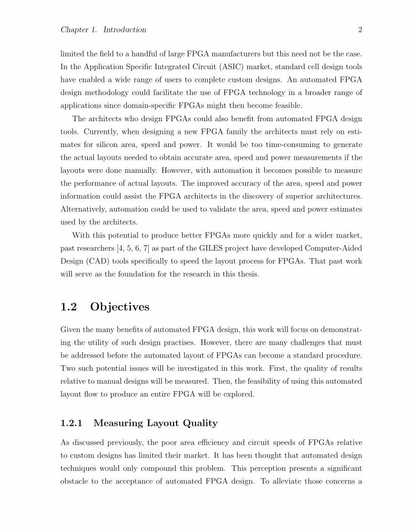
2.2 FPGA Structure
FPGAs are classified according to their routing structure. The three most common
structures are island-style, hierarchical and row-based [8]. The tools upon which this
work is based [4, 5, 6, 7] only considered island-style FPGAs and, therefore, this work will
also focus exclusively on this FPGA routing style. The island-style structure is based on
an array of identical programmable logic blocks as shown in Figure 2.1. The logic blocks
in the array are used to implement a wide range of arbitrary digital functions. The
blocks are surrounded by routing resources used for making connections both between
the blocks and to pads which connect off the array. Each individual routing resource is
known as a track. Each track may span multiple logic blocks and the number of blocks
it spans is considered to be its length. These tracks connect to the logic block through
configurable connection blocks. Connections between tracks are made by using a switch
block.
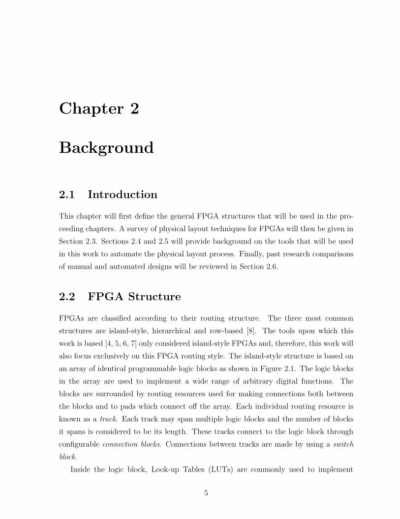
Inside the logic block, Look-up Tables (LUTs) are commonly used to implement
5
Chapter 2. Background 6
Logic Block Logic Block Logic Block Logic Block Logic Block
Logic Block Logic Block Logic Block Logic Block Logic Block
Logic Block Logic Block Logic Block Logic Block Logic Block
Logic Block Logic Block Logic Block Logic Block Logic Block
Logic Block Logic Block Logic Block Logic Block Logic Block
Routing Track Switch Block Connection BlockIO Block
Figure 2.1: FPGA Array and Pads
arbitrary boolean functions. A flip-flop is also included to allow sequential circuits to
be realized easily. Each LUT and flip-flop pair is known as a logic element. It has
been found in past work [8] that it is more efficient to have groups of logic elements
interconnected by local routing as shown in Figure 2.2. This grouping of logic elements
is called a logic cluster. The term logic block refers to the more general case of any block
with programmable logic such as a block containing a single logic element or an entire
logic cluster.
FPGA manufacturers typically create a number of similar FPGAs [9, 10] that differ
primarily in the size of the array of logic blocks. These similar FPGAs form an FPGA
BLE
BLE
N
I
. . . N
Clock
LUT
FFClock
Inputs
Basic Logic Element (BLE)
Figure 2.2: Logic Cluster from [8]
Chapter 2. Background 7
family. Within the family, logic blocks, connection blocks and switch blocks are typically
structured in the same manner. This structure, along with other essential parameters
such as the number and type of routing tracks in each dimension, describe what is
conventionally known as an FPGA architecture.
Modern commercial FPGAs have grown significantly more complex than the simple
structures portrayed above. The logic block now contains more functionality such as
carry chains to support faster arithmetic operations [9, 10]. As well, these devices now
also include heterogeneous elements such as memory or multipliers [9, 10]. However, the
simple generic programmable logic blocks described above contain the essential elements
of an FPGA. This structure retains a key property of FPGAs which is the ability to
implement arbitrary digital logic circuits. To limit the scope of this research, this work
focuses exclusively on these logic blocks and other heterogeneous elements will not be
considered.
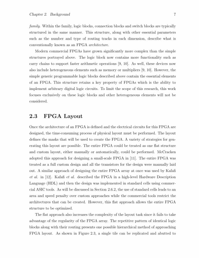
2.3 FPGA Layout
Once the architecture of an FPGA is defined and the electrical circuits for this FPGA are
designed, the time-consuming process of physical layout must be performed. The layout
defines the masks that will be used to create the FPGA. A variety of strategies for gen-
erating this layout are possible. The entire FPGA could be treated as one flat structure
and custom layout, either manually or automatically, could be performed. McCracken
adopted this approach for designing a small-scale FPGA in [11]. The entire FPGA was
treated as a full custom design and all the transistors for the design were manually laid
out. A similar approach of designing the entire FPGA array at once was used by Kafafi
et al. in [12]. Kafafi et al. described the FPGA in a high-level Hardware Description
Language (HDL) and then the design was implemented in standard cells using commer-
cial ASIC tools. As will be discussed in Section 2.6.2, the use of standard cells leads to an
area and speed penalty over custom approaches while the commercial tools restrict the
architectures that can be created. However, this flat approach allows the entire FPGA
structure to be optimized.
The flat approach also increases the complexity of the layout task since it fails to take
advantage of the regularity of the FPGA array. The repetitive pattern of identical logic
blocks along with their routing presents one possible hierarchical method of approaching
FPGA layout. As shown in Figure 2.3, a single tile can be replicated and abutted to
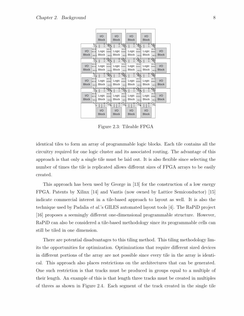
Chapter 2. Background 8
LogicBlock
LogicBlock
LogicBlock
LogicBlock
LogicBlock
LogicBlock
LogicBlock
LogicBlock
LogicBlock
LogicBlock
LogicBlock
LogicBlock
LogicBlock
LogicBlock
LogicBlock
I/OBlock
I/OBlock
I/OBlock
I/OBlock
I/OBlock
I/OBlock
I/OBlock
I/OBlock
I/OBlock
I/OBlock
I/OBlock
I/OBlock
I/OBlock
I/OBlock
I/OBlock
I/OBlock
LogicBlock
Figure 2.3: Tileable FPGA
identical tiles to form an array of programmable logic blocks. Each tile contains all the
circuitry required for one logic cluster and its associated routing. The advantage of this
approach is that only a single tile must be laid out. It is also flexible since selecting the
number of times the tile is replicated allows different sizes of FPGA arrays to be easily
created.
This approach has been used by George in [13] for the construction of a low energy
FPGA. Patents by Xilinx [14] and Vantis (now owned by Lattice Semiconductor) [15]
indicate commercial interest in a tile-based approach to layout as well. It is also the
technique used by Padalia et al.’s GILES automated layout tools [4]. The RaPiD project
[16] proposes a seemingly different one-dimensional programmable structure. However,
RaPiD can also be considered a tile-based methodology since its programmable cells can
still be tiled in one dimension.
There are potential disadvantages to this tiling method. This tiling methodology lim-
its the opportunities for optimization. Optimizations that require different sized devices
in different portions of the array are not possible since every tile in the array is identi-
cal. This approach also places restrictions on the architectures that can be generated.
One such restriction is that tracks must be produced in groups equal to a multiple of
their length. An example of this is that length three tracks must be created in multiples
of threes as shown in Figure 2.4. Each segment of the track created in the single tile
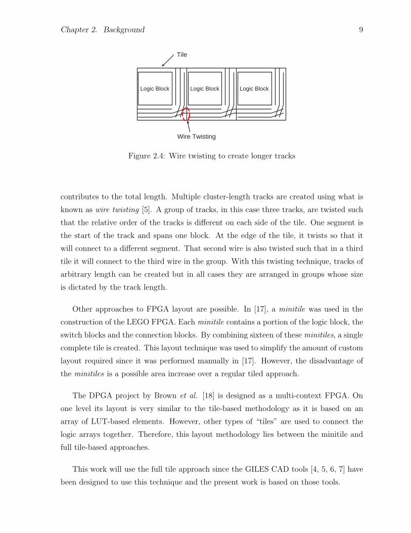
Chapter 2. Background 9
Logic Block Logic BlockLogic Block
Tile
Wire Twisting
Figure 2.4: Wire twisting to create longer tracks
contributes to the total length. Multiple cluster-length tracks are created using what is
known as wire twisting [5]. A group of tracks, in this case three tracks, are twisted such
that the relative order of the tracks is different on each side of the tile. One segment is
the start of the track and spans one block. At the edge of the tile, it twists so that it
will connect to a different segment. That second wire is also twisted such that in a third
tile it will connect to the third wire in the group. With this twisting technique, tracks of
arbitrary length can be created but in all cases they are arranged in groups whose size
is dictated by the track length.
Other approaches to FPGA layout are possible. In [17], a minitile was used in the
construction of the LEGO FPGA. Each minitile contains a portion of the logic block, the
switch blocks and the connection blocks. By combining sixteen of these minitiles, a single
complete tile is created. This layout technique was used to simplify the amount of custom
layout required since it was performed manually in [17]. However, the disadvantage of
the minitiles is a possible area increase over a regular tiled approach.
The DPGA project by Brown et al. [18] is designed as a multi-context FPGA. On
one level its layout is very similar to the tile-based methodology as it is based on an
array of LUT-based elements. However, other types of “tiles” are used to connect the
logic arrays together. Therefore, this layout methodology lies between the minitile and
full tile-based approaches.
This work will use the full tile approach since the GILES CAD tools [4, 5, 6, 7] have
been designed to use this technique and the present work is based on those tools.
Chapter 2. Background 10
ArchitectureGenerator
Placer
Router
Placement
and
Routing
ArchitectureDescription Circuit
Figure 2.5: VPR CAD Flow
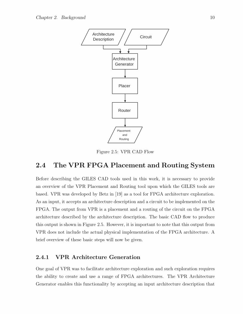
2.4 The VPR FPGA Placement and Routing System
Before describing the GILES CAD tools used in this work, it is necessary to provide
an overview of the VPR Placement and Routing tool upon which the GILES tools are
based. VPR was developed by Betz in [19] as a tool for FPGA architecture exploration.
As an input, it accepts an architecture description and a circuit to be implemented on the
FPGA. The output from VPR is a placement and a routing of the circuit on the FPGA
architecture described by the architecture description. The basic CAD flow to produce
this output is shown in Figure 2.5. However, it is important to note that this output from
VPR does not include the actual physical implementation of the FPGA architecture. A
brief overview of these basic steps will now be given.
2.4.1 VPR Architecture Generation
One goal of VPR was to facilitate architecture exploration and such exploration requires
the ability to create and use a range of FPGA architectures. The VPR Architecture
Generator enables this functionality by accepting an input architecture description that
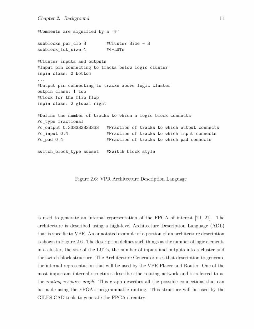
Chapter 2. Background 11
#Comments are signified by a ’#’
subblocks_per_clb 3 #Cluster Size = 3
subblock_lut_size 4 #4-LUTs
#Cluster inputs and outputs
#Input pin connecting to tracks below logic cluster
inpin class: 0 bottom
...
#Output pin connecting to tracks above logic cluster
outpin class: 1 top
#Clock for the flip flop
inpin class: 2 global right
#Define the number of tracks to which a logic block connects
Fc_type fractional
Fc_output 0.333333333333 #Fraction of tracks to which output connects
Fc_input 0.4 #Fraction of tracks to which input connects
Fc_pad 0.4 #Fraction of tracks to which pad connects
switch_block_type subset #Switch block style
Figure 2.6: VPR Architecture Description Language
is used to generate an internal representation of the FPGA of interest [20, 21]. The
architecture is described using a high-level Architecture Description Language (ADL)
that is specific to VPR. An annotated example of a portion of an architecture description
is shown in Figure 2.6. The description defines such things as the number of logic elements
in a cluster, the size of the LUTs, the number of inputs and outputs into a cluster and
the switch block structure. The Architecture Generator uses that description to generate
the internal representation that will be used by the VPR Placer and Router. One of the
most important internal structures describes the routing network and is referred to as
the routing resource graph. This graph describes all the possible connections that can
be made using the FPGA’s programmable routing. This structure will be used by the
GILES CAD tools to generate the FPGA circuitry.
Chapter 2. Background 12
2.4.2 VPR Placer and Router
Next, the VPR Placer uses the information produced by the Architecture Generator along
with the input circuit to assign logic clusters to a specific cluster within the architecture’s
array of clusters. The aim in this process is to minimize the wirelength and maximize
performance of the placement. Once a satisfactory placement has been generated, the
VPR Router uses the routing information produced by the Architecture Generator along
with the placement and the input circuit to form the connections required by the circuit.
2.5 GILES FPGA Circuit Generation and Layout
Tools
The work in [4], [5], [6], and [7] describes the development of the GILES circuit generation
and layout tools which automate the FPGA design process from a high level architecture
description to a final tile layout. These tools will serve as the foundation for this work
and, in the following sections, the capabilities of these tools prior to the present work will
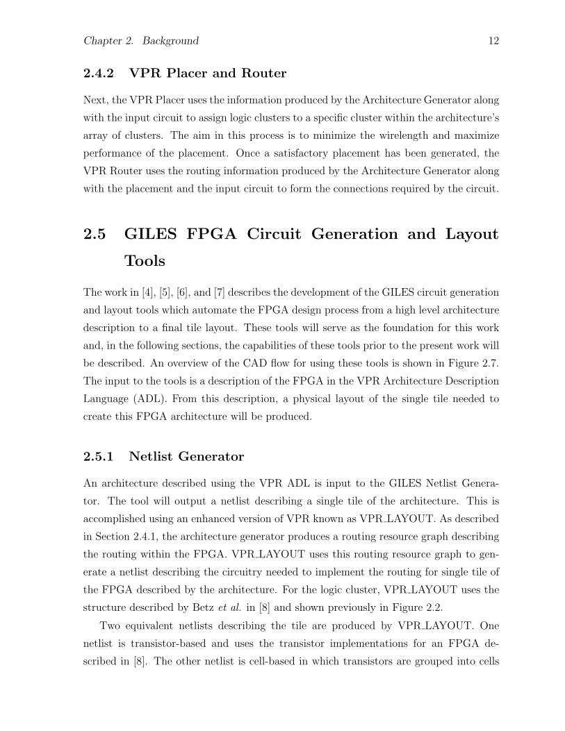
be described. An overview of the CAD flow for using these tools is shown in Figure 2.7.
The input to the tools is a description of the FPGA in the VPR Architecture Description
Language (ADL). From this description, a physical layout of the single tile needed to
create this FPGA architecture will be produced.
2.5.1 Netlist Generator
An architecture described using the VPR ADL is input to the GILES Netlist Genera-
tor. The tool will output a netlist describing a single tile of the architecture. This is
accomplished using an enhanced version of VPR known as VPR LAYOUT. As described
in Section 2.4.1, the architecture generator produces a routing resource graph describing
the routing within the FPGA. VPR LAYOUT uses this routing resource graph to gen-
erate a netlist describing the circuitry needed to implement the routing for single tile of
the FPGA described by the architecture. For the logic cluster, VPR LAYOUT uses the
structure described by Betz et al. in [8] and shown previously in Figure 2.2.
Two equivalent netlists describing the tile are produced by VPR LAYOUT. One
netlist is transistor-based and uses the transistor implementations for an FPGA de-
scribed in [8]. The other netlist is cell-based in which transistors are grouped into cells
Chapter 2. Background 13
NetlistGenerator
Cell-LevelPlacer
Inter-cellRouter
Cell-LevelNetlist
Transistor-Level Netlist
Mask-level
Layout
ArchitectureDescription
Cell-Level
Layout
Optional
Figure 2.7: GILES CAD Flow
such as inverters, SRAM bits and multiplexers. The remainder of the CAD flow uses
this cell-based netlist. Research by Egier in [22] has explored the challenge of selecting
appropriate groupings of transistors into cells. The results presented in this work will
use the best groupings found in [22].
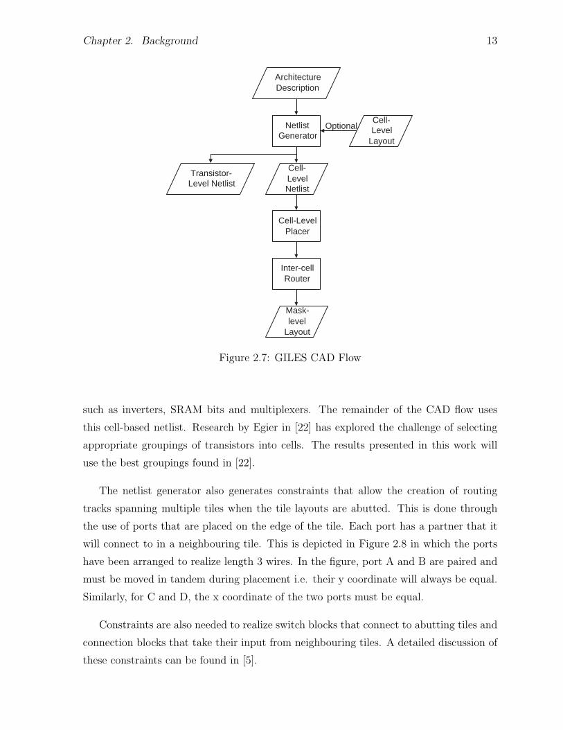
The netlist generator also generates constraints that allow the creation of routing
tracks spanning multiple tiles when the tile layouts are abutted. This is done through
the use of ports that are placed on the edge of the tile. Each port has a partner that it
will connect to in a neighbouring tile. This is depicted in Figure 2.8 in which the ports
have been arranged to realize length 3 wires. In the figure, port A and B are paired and
must be moved in tandem during placement i.e. their y coordinate will always be equal.
Similarly, for C and D, the x coordinate of the two ports must be equal.
Constraints are also needed to realize switch blocks that connect to abutting tiles and
connection blocks that take their input from neighbouring tiles. A detailed discussion of
these constraints can be found in [5].
Chapter 2. Background 14
Logic Block
A B
C
D
Figure 2.8: Single Tile with Port Constraints
2.5.2 Placement, Compaction and Routing
The port constraints and cell-level netlist are used as inputs to the GILES cell-level placer
developed by Fung in [6]. The output is a compact placement of these cells. A simulated
annealing-based algorithm is used to accomplish this task. The cells being placed vary
in both width and height. A large-tile placement is performed first in which cell-overlap
problems are avoided by operating on a large placement grid. The width and height of
each grid unit is the largest width and height respectively of all the cells. This allows
the placer to determine good global positions for the cells. Once this stage is complete,
the placer starts shrinking the tile through alternating stages of placement optimization
and tile compaction.
This custom placer makes use of FPGA-specific optimizations. In particular, the
logical equivalence of configuration SRAM is leveraged. Every programmable element
in the tile must be controlled by SRAM bits but since all the SRAM bits are identical
it is not essential that any specific bit be used. Similarly, all multiplexer inputs are
equivalent and the data and inverted data outputs of an SRAM are equivalent. By
making use of these logical equivalencies the placer is able to produce more area-efficient
layouts. However, it is significant to note that the placed netlist has been electrically
altered compared to the input netlist. When a configuration for the FPGA is produced,
Chapter 2. Background 15
these changes must be considered.
Two different routers are used in this work. Both perform the same function of routing
a placed design. The first router is the GILES router developed by Bourgeault et al. in
[7] to perform routing using an iterative maze routing algorithm. If a valid routing is not
found, the router adds rows and/or columns of space into the most congested regions of
the design and routing is attempted again. This process is repeated until a valid routing
is generated. This router was limited in multiple respects. It is unable to handle partial
blockages. If the intra-cell routing of one cell requires an additional metal layer, the
entire layer must be blocked off for inter-cell routing. As well, the router is limited to
using a relatively large routing grid to accommodate larger structures such as vias. This
limits the density of the routing that can be achieved.
An alternative approach to routing has been developed by Egier in [22] in which the
Cadence IC Craftsman router [23] is used. This router is significantly more flexible and
is therefore able to route some designs in a smaller area. A detailed discussion about the
benefits of this router can be found in [22].
Regardless of which router is used, the output from the router completes the physical
layout of an FPGA tile. This layout can then be replicated as necessary to produce an
FPGA of the desired size.
2.5.3 Previous Quality of Results using the GILES Tools
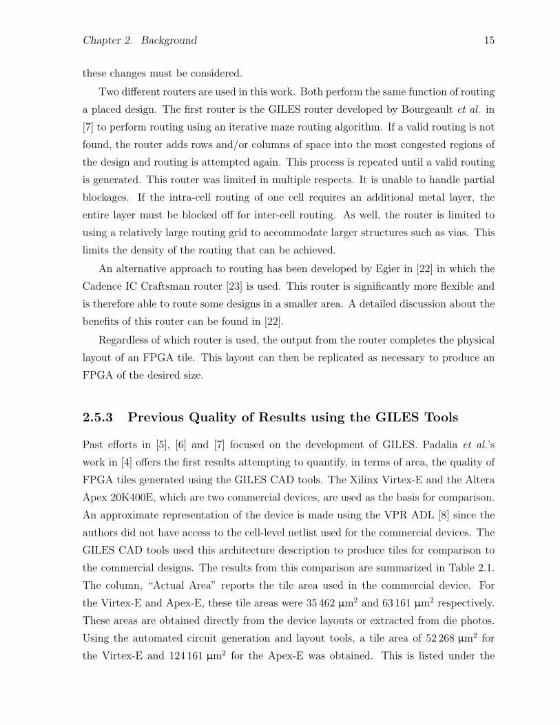
Past efforts in [5], [6] and [7] focused on the development of GILES. Padalia et al.’s
work in [4] offers the first results attempting to quantify, in terms of area, the quality of
FPGA tiles generated using the GILES CAD tools. The Xilinx Virtex-E and the Altera
Apex 20K400E, which are two commercial devices, are used as the basis for comparison.
An approximate representation of the device is made using the VPR ADL [8] since the
authors did not have access to the cell-level netlist used for the commercial devices. The
GILES CAD tools used this architecture description to produce tiles for comparison to
the commercial designs. The results from this comparison are summarized in Table 2.1.
The column, “Actual Area” reports the tile area used in the commercial device. For
the Virtex-E and Apex-E, these tile areas were 35 462 µm2 and 63 161 µm2 respectively.
These areas are obtained directly from the device layouts or extracted from die photos.
Using the automated circuit generation and layout tools, a tile area of 52 268 µm2 for
the Virtex-E and 124 161 µm2 for the Apex-E was obtained. This is listed under the
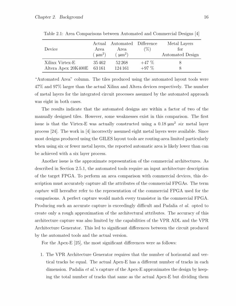
Chapter 2. Background 16
Table 2.1: Area Comparisons between Automated and Commercial Designs [4]
Actual Automated Difference Metal LayersDevice Area Area (%) for
( µm2) ( µm2) Automated Design
Xilinx Virtex-E 35 462 52 268 +47 % 8Altera Apex 20K400E 63 161 124 161 +97 % 8
“Automated Area” column. The tiles produced using the automated layout tools were
47% and 97% larger than the actual Xilinx and Altera devices respectively. The number
of metal layers for the integrated circuit processes assumed by the automated approach
was eight in both cases.
The results indicate that the automated designs are within a factor of two of the
manually designed tiles. However, some weaknesses exist in this comparison. The first
issue is that the Virtex-E was actually constructed using a 0.18 µm2 six metal layer
process [24]. The work in [4] incorrectly assumed eight metal layers were available. Since
most designs produced using the GILES layout tools are routing-area limited particularly
when using six or fewer metal layers, the reported automatic area is likely lower than can
be achieved with a six layer process.
Another issue is the approximate representation of the commercial architectures. As
described in Section 2.5.1, the automated tools require an input architecture description
of the target FPGA. To perform an area comparison with commercial devices, this de-
scription must accurately capture all the attributes of the commercial FPGAs. The term
capture will hereafter refer to the representation of the commercial FPGA used for the
comparisons. A perfect capture would match every transistor in the commercial FPGA.
Producing such an accurate capture is exceedingly difficult and Padalia et al. opted to
create only a rough approximation of the architectural attributes. The accuracy of this
architecture capture was also limited by the capabilities of the VPR ADL and the VPR
Architecture Generator. This led to significant differences between the circuit produced
by the automated tools and the actual version.
For the Apex-E [25], the most significant differences were as follows:
1. The VPR Architecture Generator requires that the number of horizontal and ver-
tical tracks be equal. The actual Apex-E has a different number of tracks in each
dimension. Padalia et al.’s capture of the Apex-E approximates the design by keep-
ing the total number of tracks that same as the actual Apex-E but dividing them

Chapter 2. Background 17
equally between the horizontal and vertical channels.
2. The Architecture Generator is designed exclusively for island-style FPGAs. The
actual Apex-E has a hierarchical style. In this hierarchy, logic elements similar
to Basic Logic Elements (BLEs) are first grouped in Logic Array Blocks (LABs)
[25] and then the LABs are grouped into MegaLABs. This structure leads to
hierarchical routing that can not be captured by the VPR ADL and, hence, Padalia
et al.’s Apex-E capture does not mimic such structures.
3. The VPR Architecture Generator assumes the logic clusters consist of the simple
BLEs shown previously in Figure 2.2. The actual Apex-E contains additional cir-
cuitry to support carry chains for faster addition and cascade chains for realizing
wide functions. These features were simply ignored by Padalia et al..
For the Virtex-E [24], the most significant differences are listed below.
1. The VPR ADL assumes all routing tracks are bidirectional. In the actual Virtex-E,
some of the tracks are only driven at one end. The Virtex-E capture in [4] treats
these unidirectional lines as regular bidirectional tracks.
2. Like the Apex-E, the actual Virtex-E contains logic clusters with additional cir-
cuitry. Carry chains are included to speed circuits which perform addition. The
LUTs can be connected to act as a 5-LUT and they can also be configured to behave
as RAMs. Again, these differences were not included in Padalia et al.’s capture.
These inaccuracies in both the Virtex-E and Apex-E capture are significant and this
potentially calls in to question the validity of the comparison in [4].
The extent of these differences can be measured by comparing the number of SRAM
configuration bits in a single tile of the automated and commercial designs. This com-
parison is summarized in Table 2.2 with the bit counts listed per FPGA tile. The con-
figuration SRAM count labelled as the “Actual SRAM Bits” count is an estimate of the
number of bits in the true Virtex-E and Apex-E based on the configuration information
provided in [26] and [25]. For the Virtex-E and Apex 20K400E, this estimate is 864 and
2349 bits respectively. The estimate for the Apex 20K400E is more approximate because
Altera does not provide detailed information about which portion of the configuration
bitstream is allocated to each tile. The estimate was produced by dividing the total
configuration bitstream length by the number of tiles in the device. This clearly ignores

Chapter 2. Background 18
Table 2.2: SRAM Count of Automated and Commercial Designs
Actual SRAM bitsDevice SRAM used by
bits [4]
Xilinx Virtex-E 864 669Altera Apex 20K400E 2349 1230
all the configuration in the periphery as well as any padding that may be present in the
bitstream. The number of configuration bits used in [4]’s automated representation is
669 and 1230 for the Xilinx and Altera devices respectively. In both cases the difference
with respect to the actual device is over 20%. This is significant and it reveals that the
architecture description used in [4] bears only slight similarity to the actual architecture.
This is an unfortunate shortcoming since it prevents a reliable assessment of the state
of automated FPGA design. A more precise comparison is clearly needed and this work
will address this issue by developing an accurate comparison.
2.6 Alternative Automated Layout Methodologies
The work in this thesis is an attempt to automate a design process that has tradition-
ally been performed as a full custom manual design. Numerous alternate automation
methodologies exist ranging from transistor-based to cell-based techniques. Some of the
approaches that have been used in the past and their results relative to full-custom
manual design will be reviewed in the following sections.
2.6.1 Transistor-Based Methodologies
All digital microelectronic circuits are composed of transistors. This is the lowest level
unit that can be easily considered by placement and routing tools. One possibility then
for automatic layout is to simply place and route the transistors that constitute the
design. Such approaches are termed transistor-based methodologies. This has been a rich
research area and various past efforts will be reviewed.
Most past work has focused on applying this transistor-based approach to fixed-
height cell design. One technique popularized by Uehara and van Cleemput in [27] is
a one-dimensional technique where two parallel n and p diffusion regions are used for
implementing transistors. Power rails run parallel to these rows. In [28], Hsieh et al.
Chapter 2. Background 19
modified this general one-dimensional approach to allow routing anywhere between the
power and ground rails. One challenge faced by Hsieh et al. is ensuring diffusion sharing
is used where possible. Opportunities for diffusion region sharing emerge when two tran-
sistors share a common source or drain. To ensure as many such opportunities are used,
Hsieh et al. use an optimal chaining algorithm. For larger transistors, a folding algorithm
was developed to divide those larger transistors into multiple fingers. A comparison with
manual cell layouts was then performed for multiple cells. The automatically generated
layouts ranged from 17% smaller to 8% larger for cells having between 4 and 28 transis-
tors. A total of six cells were compared and in four of them the automatically generated
layout proved to be larger.
Hwang et al. in [29] were able to improve on the results obtained by Hsieh et al. For
twenty-four cells with transistor counts ranging from 2 to 32, Hwang et al.’s layouts were
on average 4% larger than manual layouts of the same cells. The best result obtained was
18% smaller than the manual layout and the worst result was 17% larger. However, both
the manual and automated layouts used the same layout style of one-dimensional rows
of n and p transistors. With more freedom a human designer might be able to achieve
better results than are possible when confined to a specific style.
This incomplete success with one dimensional layout motivated later work that pur-
sued a two-dimensional style. Using a two-dimensional style, transistors can be placed
both horizontally and vertically. This is more like manual custom design as the con-
cept of rows is eliminated. In the AKORD project [30] and later follow up work [31],
this placement style was used for designing data path layouts. The placement tool is
simulated-annealing based and supports moves such as transistor folding and diffusion
merging. With this tool, one benchmark circuit was 8.7% smaller than a manual design
but the remainder of the designs ranged from 0% to 18% larger. All the circuits however
contained fewer than 72 transistors.
Clearly, with the transistor-based methodology, there is a great deal of freedom in the
optimizations possible and the results with these tools approach the area quality achieved
by manual designers. The run times reported for these transistor-based methodologies
were on the order of minutes [30] which is reasonable. However, none of these past
researchers considered the issue of scaling these techniques to handle the approximately
10 000 transistors typically found in an FPGA tile. Therefore, it remains an open question
as to whether this transistor-based design methodology can accommodate large designs
like FPGA tiles.

Chapter 2. Background 20
GND
VDD
GND
VDD
GND
VDD
GND
VDD
INVERTER BUFFERAOI MUX
Figure 2.9: Standard Cell Design Style
2.6.2 Standard Cell Based Design
An alternative to operating on the transistor level is to group transistors into cells.
Typically, these groupings form cells that implement various logic gates ranging from
simple inverters, AND gates, and multiplexers to more complex AND-OR-INVERT gates,
adders and flip-flops [32, 33]. While a range of cell-based techniques are possible, the most
frequently used style is standard cell design. An example of this is shown in Figure 2.9.
With standard cells, all cells regardless of functionality have the same fixed height and
only the cell’s width varies [33]. Power and ground rails run the full width of the cell. This
allows the power and ground connections to be made simply by abutting cells. In the past,
additional space was needed for routing channels [33]. However, with the numerous metal
layers available in modern processes, this is no longer necessary and typically routing can
be performed over the placed cells [32, 34]. With this standard cell-based approach,
the user need only be concerned with the connections between cells thereby avoiding
many complex layout issues. Numerous vendors such as Artisan Components [35] and
Virtual Silicon Technology [36] now offer standard cell libraries for various processes.
These libraries are pre-characterized and come in a range of cells over a discrete range
of drive strengths. With these libraries, a designer can easily create new designs using
commercial tools, such as those from Cadence [37, 38] and Synopsys [39], which automate
synthesis, placement and routing. The automated tools allow the user to easily control
target parameters such as aspect ratio and row utilization. Aspect ratio refers to the
ratio of layout height to width or vice versa. Row utilization is calculated as the total
area of the standard cells relative to the total area available for placement [32]. It is
reported as a percentage and it indicates the area efficiency or density of the design.
Lower values simplify both placement and routing while higher values make the design
more area-efficient. This standard cell approach has been widely adopted for the design
of ASICs in industry [32, 33].
Despite this widespread adoption of standard cell design, it is widely felt that it too

Chapter 2. Background 21
Table 2.3: Comparison of Design Techniques from [40]
Custom Crafted Bit-sliced FullyCells Standard Automated
Cells Std Cells
Area 1.0 1.64 5.25 14.50Delay 1.0 1.11 2.23 N/AM2 Length 1.0 1.07 4.19 34.9M3 Length 1.0 1.63 2.52 7.92
does not deliver the area and speed performance that would be possible with manual
full custom design. Dally and Chang in [40] examined this issue for data path circuits.
The authors explored four different design techniques. The first technique is the full
custom manual approach. With this approach, extensive global and local wire planning
is performed. The structure of the design is also preserved by recognizing the regularity
of the bit slices. Finally, transistors are also sized to match the load they will drive.
The next approach considered was the crafted cell approach. With this layout technique,
the standard cell library is augmented with additional cells required by the design. For
instance, a register cell which requires six library cells is implemented as one of the
crafted cells. A manual synthesis process was performed for a single bit slice. Placement
was also manual but final routing was automated. The data path is then completed
by tiling the individual bit slices. Another alternative that was explored was the bit-
sliced standard cell approach. With this technique, the entire design process including
synthesis, placement and routing was performed using automated tools for a single bit
slice. The basic standard cell library without the additional crafted cells was used. The
bit slices were again replicated to complete the data path. The final approach considered
is fully automated standard cell design. Starting from a Verilog description, the entire
design process is performed automatically for the entire data path. Again, the basic
standard cell library is used as the target library. All design approaches used only static
CMOS circuitry.
The results obtained by Dally and Chang are summarized in Table 2.3. The data
clearly demonstrates that the full custom approach offers the best performance over the
range of parameters considered. The area measurements showed that the best automated
technique, the crafted cell approach, was 64% larger than the full custom design. This
demonstrates that future tools will need to capture more human intuition if the auto-
mated tools are ever to equal or surpass the layout density acheived by manual designers.

Chapter 2. Background 22
The authors also report that the area increase is at least partly due to the routing grid
required by the automated router.
In terms of delay through the data path, there is significantly less variation in the
results relative to the full-custom design. The crafted cell approach is only 11% slower
than the custom design but was produced with a fraction of the effort. This is an
interesting result which suggests automated layout tools may offer a potential trade off
of time to market and increased processing cost due to the increased area.
The authors also report the metal layer 2 and 3 wirelengths. Here the automated
approach again performs significantly worse than custom. The crafted cell technique has
7% and 63% longer wirelength on metal layers 2 and 3 than the full custom design. Due
to the larger area required for the crafted cell design, the wirelength was expected to
be longer than the full-custom design; however, the increased area does not justify the
63% increase in metal 3 length. Dally and Chang suggest that the full-custom design
benefited from a “wires-first“ approach in which wire planning is undertaken early in the
design process. The automated tools currently do not perform such early wire planning
and the authors suggest that future automated design flows should be wiring-centric.
The other design techniques, bit-sliced and fully automated, perform significantly
worse than the crafted cell approach. There is clearly a significant advantage to recog-
nizing the hierarchy present in a design. It is also apparent that a library augmented
with cells specific to the design offers considerable area and delay savings.
These results are specific to a data path but it clearly suggests that standard cells
incur significant overhead relative to custom designs. This result will likely apply to
FPGA design as well. The tile-based approach used by the GILES tools is somewhat
similar to the crafted cell technique. With the GILES automated circuit generation tools,
the synthesis process is automated but has been tailored specifically to FPGAs. As well,
the idea of laying out a single tile and replicating it is very much like the idea of tiling
bit-slices. Therefore, this suggests that area results between 1.64 and 5.25 times larger
than manual should be possible using the GILES automated layout tools although the
number of transistors that must be laid out by the GILES tools is much larger.
Standard cells have also been used in programmable architectures such as the Totem
Project [16]. Totem focuses on Domain-Specific Reconfigurable systems and it can target
a range of programmable circuit implementations. The approach uses a standard ASIC
flow starting from behavioural Verilog. A Synopsys tool was used to synthesize the de-
sign into a library of standard cells that has been augmented to include FPGA specific
Chapter 2. Background 23
cells. Cadence Silicon Ensemble [38] was then used to place and route the design. Row
utilization was set to the highest value for which the design was routable. Using this
methodology, it was found that standard cell tools can produce a design that is 270%
larger than a full custom manual design. This project also allows for the design to be
optimized producing less flexible programmable designs. Using domain specific architec-
tural reductions, the standard cell design can be made 2.1x smaller than the complete
full-custom implementation. The ability to easily regenerate new designs highlights one
of the benefits of automated design but the area result clearly demonstrates that, in the
direct comparison, standard cells lead to a significant area increase.
Kafafi et al. in [12] also used a standard cell design methodology for designing em-
bedded programmable logic cores. A standard ASIC flow was used with synthesis in
Synopsys and physical design in Cadence. This ASIC flow restricted the programmable
architecture to one having a directional bias. The directional architecture eliminates the
combinational loops that cause problems for synthesis tools but it is less flexible since
the routing only flows in one direction. Using such an architecture, Kafafi et al. created
a design consisting of a directional 4 by 4 array of 3-LUTs. This design required an
area of 81 092 µm2 when produced using the ASIC tools. For comparison, the authors
estimated the size of the custom layout. The estimated custom area for the same design
was 12 868 µm2 which is 84% smaller than the version created with the commercial tools.
These results from past researchers suggest that the standard cell design methodology
has the capacity to handle programmable designs such as an FPGA tile which contains
on the order hundreds to thousands of cells [7]. However, this approach appears to
consistently incur a significant overhead with respect to custom designs. One of the
goals of this work is to reduce this difference eventually allowing automated designs to
surpass the area efficiency of manual layouts.

Chapter 3
Area Efficiency Measurement of
Automated FPGA Layout
3.1 Introduction
The goal of this research is to demonstrate the utility of automated FPGA design and
layout. The utility of these techniques depends in part on the ability of the automated
system to produce high quality layouts. This chapter will assess the quality of FPGA
layouts produced by the GILES layout tools [4] through an area comparison between
automatically-generated and manually-created designs. To make this a fair comparison,
an accurate capture of a commercial device, the Xilinx Virtex-E [24], will be used and this
capture will be presented in Section 3.2. The accuracy of this capture will be measured in
Section 3.3. Then, in Section 3.4, this capture of the Virtex-E will serve as the basis for
comparisons between automatically-generated and manually-created layouts. For these
comparisons, the automated layout will be performed using the GILES layout system
that was introduced in Chapter 2. An alternate approach to the GILES layout system is
to use commercial standard cell-based tools and, in Section 3.5, the area results of these
two automated methodologies will be compared. Finally, the results from all the design
styles will be summarized in Section 3.6.
3.2 Accurate Capture of Virtex-E Circuit
The aim of accurately comparing manually-created and automatically-generated layout
areas requires that similar, or ideally identical, circuits are used as the basis for com-
24
Chapter 3. Area Efficiency Measurement of Automated FPGA Layout 25
parison. As described in Chapter 2, the prior work by Padalia et al. [4] used a very
approximate capture of the Virtex-E and the Apex-E, which called the validity of the
comparison into question. One issue that was ignored by Padalia et al., is that this
capture, which was previously defined to describe a representation of a target FPGA,
can have varying degrees of detail. At the highest level of abstraction, an architectural
capture encapsulates all the logical attributes of an FPGA. This was the level of accu-
racy sought by Padalia et al. [4]. Such an architectural capture ensures identical logical
functionality; however, there are many possible circuits that implement this functional-
ity. Therefore, a more detailed description of the device, called a circuit-level capture, is
needed to describe the circuits used in the target FPGA to realize the logical behaviour
of the architectural capture. As an example, this circuit-level capture would correctly
describe whether switches are implemented using a single driver and a multiplexer or
using multiple tri-state buffers. At this level of accuracy, the number of transistors in
the capture should match the number in the FPGA being captured. This however does
not address the issue of sizing these transistors and a more comprehensive electrical cap-
ture describes these details. An accurate electrical capture should describe an electrically
identical device. When comparing layout methodologies exclusively, this level of accuracy
is required and such accuracy will be sought in this work.
The difficulty in producing such an accurate capture of a commercial device is that
the netlists describing the circuits in the FPGAs are generally not publicly available.
Therefore, to create a capture, a specific FPGA was reverse engineered in this work.
Unlike Padalia et al.’s [4] capture, this new electrical capture was not restricted by the
semantics of the VPR ADL since a new set of tools was developed to produce the capture.
Even with these new tools creating an accurate electrical capture is a time-consuming
process and this work only attempted one such capture. The device selected for this
capture was the Xilinx Virtex-E for the following reasons:
1. The availability of the Xilinx FPGA Editor [41] which shows all the possible connec-
tions available in a Xilinx FPGA. Such information is necessary to reverse-engineer
a device.
2. The island-style structure of the Virtex-E is well-suited to the tile-based layout
methodology.
3. The TSMC 0.18 µm process available at the University of Toronto through the
Canadian Microelectronics Corporation (CMC) is similar to the process from UMC
used by Xilinx for the Virtex-E. This means that layout design rules will be com-
Chapter 3. Area Efficiency Measurement of Automated FPGA Layout 26
LUT
LUT
Carry &Control
Carry &Control
COUT
YBY
YQ
XB
XQ
X
SPD Q
CE
RC
SPD Q
CE
RC
G4
G3
G1
G2
BY
F4F3
F2F1
BX
CIN
LUT
LUT
Carry &Control
Carry &Control
COUT
YBY
YQ
XB
XQ
X
SPD Q
CE
RC
SPD Q
CE
RC
G4
G3
G1
G2
BY
F4F3
F2F1
BX
CIN
Slice 0Slice 1
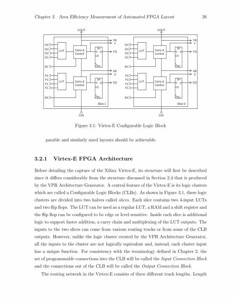
Figure 3.1: Virtex-E Configurable Logic Block
parable and similarly sized layouts should be achievable.
3.2.1 Virtex-E FPGA Architecture
Before detailing the capture of the Xilinx Virtex-E, its structure will first be described
since it differs considerably from the structure discussed in Section 2.4 that is produced
by the VPR Architecture Generator. A central feature of the Virtex-E is its logic clusters
which are called a Configurable Logic Blocks (CLBs). As shown in Figure 3.1, these logic
clusters are divided into two halves called slices. Each slice contains two 4-input LUTs
and two flip flops. The LUT can be used as a regular LUT, a RAM and a shift register and
the flip flop can be configured to be edge or level sensitive. Inside each slice is additional
logic to support faster addition, a carry chain and multiplexing of the LUT outputs. The
inputs to the two slices can come from various routing tracks or from some of the CLB
outputs. However, unlike the logic cluster created by the VPR Architecture Generator,
all the inputs to the cluster are not logically equivalent and, instead, each cluster input
has a unique function. For consistency with the terminology defined in Chapter 2, the
set of programmable connections into the CLB will be called the Input Connection Block
and the connections out of the CLB will be called the Output Connection Block.
The routing network in the Virtex-E consists of three different track lengths. Length
Chapter 3. Area Efficiency Measurement of Automated FPGA Layout 27
one tracks connect to each of the neighbouring CLBs and there are twenty-four such
connections in each direction. In each dimension there are also seventy-two length six
tracks. Two thirds of these lines are only driven at one end and are called unidirectional
routing tracks. This is a significant difference compared to the routing created by the
VPR Architecture Generator since all the tracks it creates can be driven at either end.
The remaining one third of the tracks can be driven at either end and will be called
bidirectional tracks. Twelve buffered long lines that span the entire length of chip are
provided in both dimensions as well. Finally, there are also four tri-state busses in the
horizontal direction. These resources are connected to each other through a switch block-
like structure. Xilinx refers to this as a General Routing Matrix (GRM).
3.2.2 Methodology
The process of producing an accurate electrical capture begins with an architectural
capture. That capture is then refined to produce a circuit-level capture. Finally, the
transistors in the circuit are sized and a complete electrical capture is generated. The
process used to create each of these captures is described in the following sections.
Architectural Capture
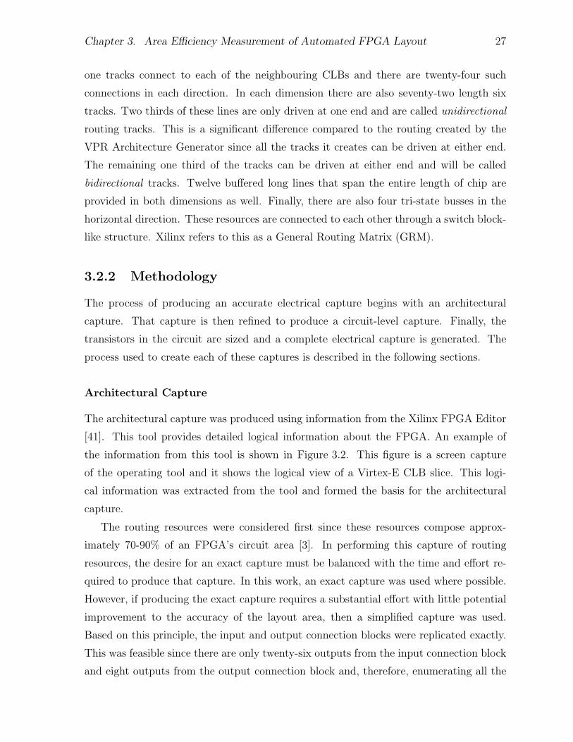
The architectural capture was produced using information from the Xilinx FPGA Editor
[41]. This tool provides detailed logical information about the FPGA. An example of
the information from this tool is shown in Figure 3.2. This figure is a screen capture
of the operating tool and it shows the logical view of a Virtex-E CLB slice. This logi-
cal information was extracted from the tool and formed the basis for the architectural
capture.
The routing resources were considered first since these resources compose approx-
imately 70-90% of an FPGA’s circuit area [3]. In performing this capture of routing
resources, the desire for an exact capture must be balanced with the time and effort re-
quired to produce that capture. In this work, an exact capture was used where possible.
However, if producing the exact capture requires a substantial effort with little potential
improvement to the accuracy of the layout area, then a simplified capture was used.
Based on this principle, the input and output connection blocks were replicated exactly.
This was feasible since there are only twenty-six outputs from the input connection block
and eight outputs from the output connection block and, therefore, enumerating all the
Chapter 3. Area Efficiency Measurement of Automated FPGA Layout 28
SYNC
ASYNC
RESET TYPE
HIGH
LOW
F
G
LOW
HIGH
CELATCH
CK
DFF
Q
INIT REV
REVINIT
QFF
D
CKLATCH
CE
G4
ROM
RAM
LUT
A2
A1WS
A4
A3
DI
D
1
0
1
SR
SR_B
0
1
CE
CE_B
0
1
BX
BX_B
CIN
1
0
SR
CLK
0
1
0
CE
0
1
BX
0
0 0
1
F1
PROD
1
0
1
BY
BY_B
F1
F2
F3
F4
F5IN
0
1
G1
BY
G3
G2
DIWS
A1
A2
A3
A4
RAM
ROM
LUTD
BY
BX
DG
DF
CIN
BX
A5 WSG
WSFCK
WE
1
F
1 OUTS00 1
1
0
1
G1
PROD
0
FXOR
F
F5
0
1
0
0
1
0
1
XQ
0
0
X
F5
0 X B
YQ
1SHIFT
16X1DP
32X1
16X2
16X1
2SHIFTS
G
11S00 1
OUT
GXOR
F6
G
0
1
0 Y
YB
COUT0
BAL_LOGIC1_208
BAL_LOGIC0_164
Figure 3.2: Logical View of Virtex-E Slice from Xilinx FPGA Editor
connections was a manageable task. However, for the switch block an exact capture
would require significant effort since it has over sixty-four tracks with hundreds of pos-
sible sources. To produce the capture in a reasonable amount of time, only the number
and type of connections were captured and the tracks were interconnected randomly.
For the logic block, all the connections shown in FPGA Editor were replicated except
for an advanced mode which allows many LUTs to be connected together to form a shift
register. This behaviour was not included in the architectural capture again because of
the significant effort it would entail.
Circuit-Level Capture
Next, the complete architectural capture was mapped to specific electrical circuits that
realize the desired behaviour. It was necessary to make some assumptions since this
circuit-level information is not provided in any Xilinx data sheets or in the Xilinx FPGA
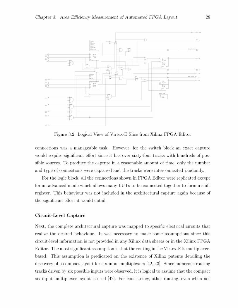
Editor. The most significant assumption is that the routing in the Virtex-E is multiplexer-
based. This assumption is predicated on the existence of Xilinx patents detailing the
discovery of a compact layout for six-input multiplexers [42, 43]. Since numerous routing
tracks driven by six possible inputs were observed, it is logical to assume that the compact
six-input multiplexer layout is used [42]. For consistency, other routing, even when not
Chapter 3. Area Efficiency Measurement of Automated FPGA Layout 29
......
Unidirectional Routing Track
Bidirectional Routing Track
TrackInput
Track
Input
Track
Input...
Track
Output
Track Output Track Output
Figure 3.3: Routing Track Structure
driven by six potential inputs, is also assumed to be multiplexer-based.
Given this assumption, the structure used for routing tracks is shown in Figure 3.3.
The select lines for the multiplexers and the connections to the gates of transistors con-
trolled by configuration SRAM bits are not shown in the diagram. For bidirectional
tracks, it is assumed that multiplexers followed by tristate buffers are used to drive the
tracks. As can be seen in the figure, an NMOS pass transistor is used to implement the
tristate functionality.
For the logic block, translating the architectural features to circuits is straightforward
in most cases. Elements shown as multiplexers in the FPGA Editor are assumed to be
implemented as multiplexers composed of NMOS pass transistors. This is a sensible
choice since it provides reasonable speed in minimal area. However, for some blocks, the
circuit-level implementation is not transparent. This applies in particular to the LUT and
flip-flop, which differ significantly from the simple structures used by the GILES circuit
generation tools [5]. Patents from Xilinx, [44] and [45], were used to determine the
circuitry for these elements respectively and the circuits were replicated where possible.
The patents do not show some portions of these blocks in detail and, hence, only an
approximation of these segments is possible.
Electrical Capture
To make the most accurate capture, it is necessary to determine proper transistor sizes
for each of the the circuit elements. Most cells including the multiplexers, flip-flops and
configuration SRAM bits are implemented using minimum-width transistors. This is
reasonable since it minimizes both the area and the capacitive load on other elements.
Chapter 3. Area Efficiency Measurement of Automated FPGA Layout 30
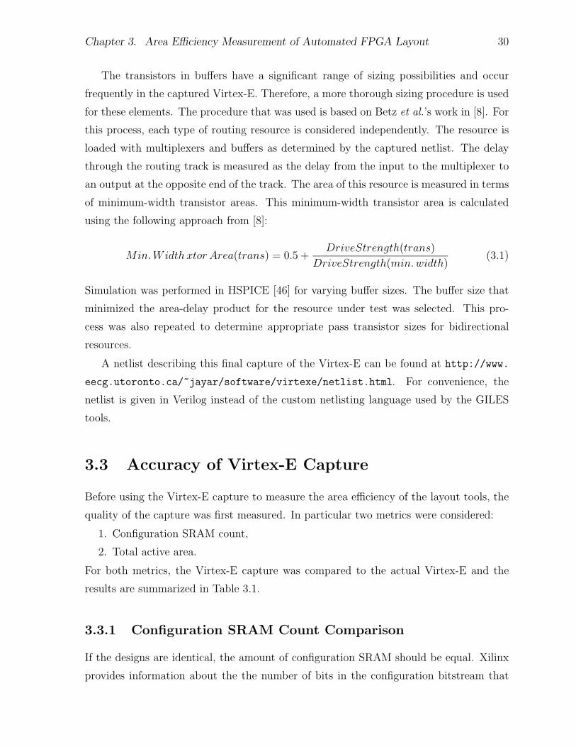
The transistors in buffers have a significant range of sizing possibilities and occur
frequently in the captured Virtex-E. Therefore, a more thorough sizing procedure is used
for these elements. The procedure that was used is based on Betz et al.’s work in [8]. For
this process, each type of routing resource is considered independently. The resource is
loaded with multiplexers and buffers as determined by the captured netlist. The delay
through the routing track is measured as the delay from the input to the multiplexer to
an output at the opposite end of the track. The area of this resource is measured in terms
of minimum-width transistor areas. This minimum-width transistor area is calculated
using the following approach from [8]:
Min.Width xtor Area(trans) = 0.5 +DriveStrength(trans)
DriveStrength(min.width)(3.1)
Simulation was performed in HSPICE [46] for varying buffer sizes. The buffer size that
minimized the area-delay product for the resource under test was selected. This pro-
cess was also repeated to determine appropriate pass transistor sizes for bidirectional
resources.
A netlist describing this final capture of the Virtex-E can be found at http://www.
eecg.utoronto.ca/~jayar/software/virtexe/netlist.html. For convenience, the
netlist is given in Verilog instead of the custom netlisting language used by the GILES
tools.
3.3 Accuracy of Virtex-E Capture
Before using the Virtex-E capture to measure the area efficiency of the layout tools, the
quality of the capture was first measured. In particular two metrics were considered:
1. Configuration SRAM count,
2. Total active area.
For both metrics, the Virtex-E capture was compared to the actual Virtex-E and the
results are summarized in Table 3.1.
3.3.1 Configuration SRAM Count Comparison
If the designs are identical, the amount of configuration SRAM should be equal. Xilinx
provides information about the the number of bits in the configuration bitstream that
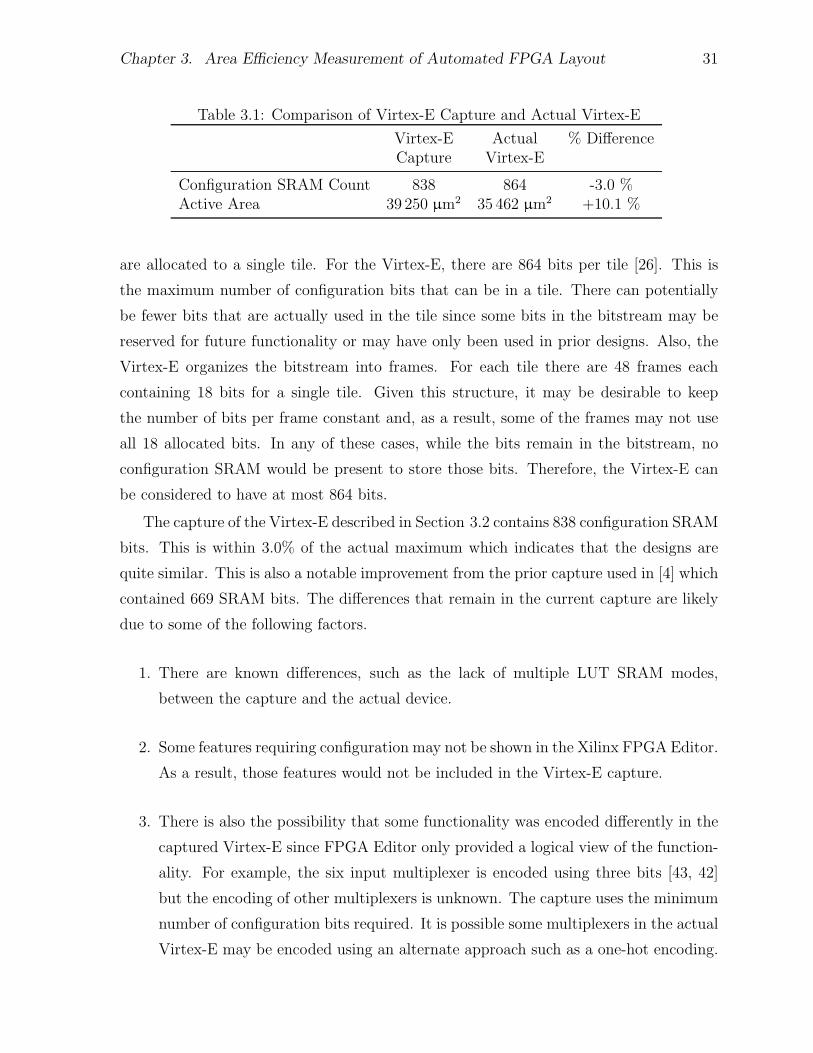
Chapter 3. Area Efficiency Measurement of Automated FPGA Layout 31
Table 3.1: Comparison of Virtex-E Capture and Actual Virtex-E
Virtex-E Actual % DifferenceCapture Virtex-E
Configuration SRAM Count 838 864 -3.0 %Active Area 39 250 µm2 35 462 µm2 +10.1 %
are allocated to a single tile. For the Virtex-E, there are 864 bits per tile [26]. This is
the maximum number of configuration bits that can be in a tile. There can potentially
be fewer bits that are actually used in the tile since some bits in the bitstream may be
reserved for future functionality or may have only been used in prior designs. Also, the
Virtex-E organizes the bitstream into frames. For each tile there are 48 frames each
containing 18 bits for a single tile. Given this structure, it may be desirable to keep
the number of bits per frame constant and, as a result, some of the frames may not use
all 18 allocated bits. In any of these cases, while the bits remain in the bitstream, no
configuration SRAM would be present to store those bits. Therefore, the Virtex-E can
be considered to have at most 864 bits.
The capture of the Virtex-E described in Section 3.2 contains 838 configuration SRAM
bits. This is within 3.0% of the actual maximum which indicates that the designs are
quite similar. This is also a notable improvement from the prior capture used in [4] which
contained 669 SRAM bits. The differences that remain in the current capture are likely
due to some of the following factors.
1. There are known differences, such as the lack of multiple LUT SRAM modes,
between the capture and the actual device.
2. Some features requiring configuration may not be shown in the Xilinx FPGA Editor.
As a result, those features would not be included in the Virtex-E capture.
3. There is also the possibility that some functionality was encoded differently in the
captured Virtex-E since FPGA Editor only provided a logical view of the function-
ality. For example, the six input multiplexer is encoded using three bits [43, 42]
but the encoding of other multiplexers is unknown. The capture uses the minimum
number of configuration bits required. It is possible some multiplexers in the actual
Virtex-E may be encoded using an alternate approach such as a one-hot encoding.
Chapter 3. Area Efficiency Measurement of Automated FPGA Layout 32
3.3.2 Active Area Comparison
Identical designs should also have identical active areas. Betz et al. in [8] stated that
FPGA manufacturers report that their designs tend to be active area-limited. Hence, the
total tile area can be used as a measure of the transistor area required for the design. As
shown in Table 3.1, this gives an active area of 35 462 µm2 for the actual Virtex-E. For the
Virtex-E capture, the active area is calculated as the sum of the areas for each individual
cell in the netlist. By this measure, the capture has a total active area of 39 250 µm2
which is within 10.1% of the actual area. This indicates both that a similar amount of
circuitry is being used in the Virtex-E capture and that the area estimator is producing
results that will allow for a conservative comparison between the automatically-generated
and manually-created designs.
There are a few possible reasons why the Virtex-E capture has a larger active area
than the actual Virtex-E. One factor is that there is an area overhead associated with the
cell-based approach used by the automated layout tools. This overhead is a result of a
border of empty space that must be left around every cell layout to satisfy all the design
rules. In many cases, this border is excessively conservative but it is necessary because
the automated layout tools are not aware of the cell contents and their associated design
rules. The empty space is included as part of the total active area and, therefore, this
contributes to the capture’s larger active area. Another possible factor is the cell layouts
used in the Virtex-E capture may not be as area efficient as those produced by skilled
designers. At Xilinx, significant time is likely spent producing extremely dense layouts.
For example, an efficient six-input multiplexer layout described in [42] has even been
patented. Xilinx also has gone further and, in [43], a compact layout is described for
two six-input multiplexers that share some common inputs. The Virtex-E capture from
Section 3.2 does not take advantage of such opportunities. Therefore, with less efficient
layouts, the larger cell area for the Virtex-E capture is not surprising.
3.4 Automated and Manual Layout Area Compar-
isons
The goal of determining the quality of an automatically generated FPGA layout requires
an accurate comparison to manual created layouts. In this section, the accurate Virtex-
E capture described in Section 3.2 is used with the GILES automated layout tools to
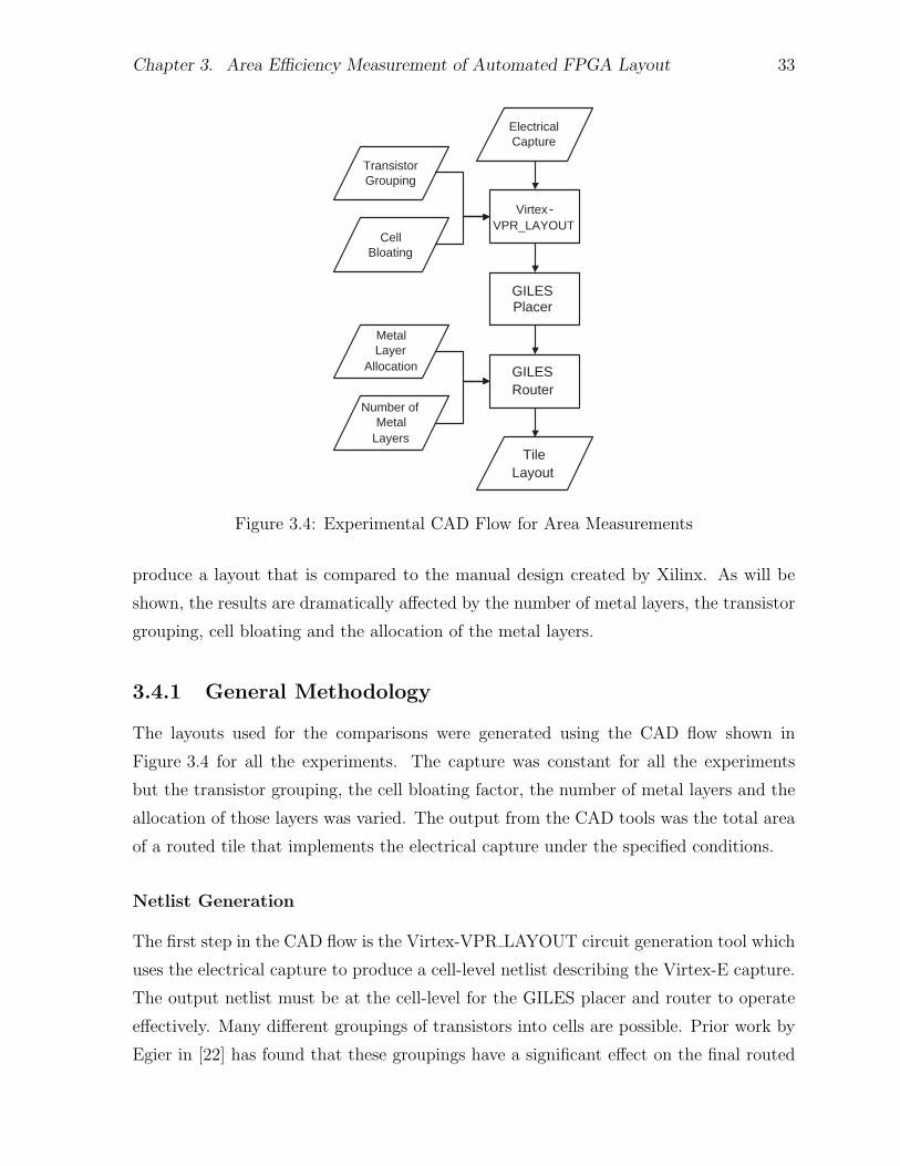
Chapter 3. Area Efficiency Measurement of Automated FPGA Layout 33
Virtex-VPR_LAYOUT
GILESPlacer
GILESRouter
TileLayout
ElectricalCapture
MetalLayer
Allocation
TransistorGrouping
CellBloating
Number ofMetal
Layers
Figure 3.4: Experimental CAD Flow for Area Measurements
produce a layout that is compared to the manual design created by Xilinx. As will be
shown, the results are dramatically affected by the number of metal layers, the transistor
grouping, cell bloating and the allocation of the metal layers.
3.4.1 General Methodology
The layouts used for the comparisons were generated using the CAD flow shown in
Figure 3.4 for all the experiments. The capture was constant for all the experiments
but the transistor grouping, the cell bloating factor, the number of metal layers and the
allocation of those layers was varied. The output from the CAD tools was the total area
of a routed tile that implements the electrical capture under the specified conditions.
Netlist Generation
The first step in the CAD flow is the Virtex-VPR LAYOUT circuit generation tool which
uses the electrical capture to produce a cell-level netlist describing the Virtex-E capture.
The output netlist must be at the cell-level for the GILES placer and router to operate
effectively. Many different groupings of transistors into cells are possible. Prior work by
Egier in [22] has found that these groupings have a significant effect on the final routed
Chapter 3. Area Efficiency Measurement of Automated FPGA Layout 34
area because a boundary of white space around the cells must be added to satisfy the
design rules (in particular, the n-well spacing rules) since the GILES layout tools are
unaware of the cell contents. The effect of transistor groupings on the Virtex-E capture’s
layout area is examined in Section 3.4.3.
Since there are various possible transistor groupings, there are a large number of
possible cells required by the GILES tools. The area of each cell must be known by the
GILES tools but it is not feasible to manually construct all these cells. Instead of creating
each cell, an estimated area will be used. Egier in [22] developed a model to produce
these area estimates. It is based on Betz et al.’s approach from [8] of using minimum-
width transistor areas to model area. Egier’s area model was found to estimate the cell
area with an average absolute error of 5.8% relative to some test manual layouts. Over a
range of architectures, the final routed area using cells with estimated areas was between
3.2% and 8.0% larger than when manual cells were used. This accuracy was considered
sufficient for the comparisons that were performed in this work. In Section 3.4.4, the
estimated cell areas are increased by a common factor and the area effect of that change
is observed.
The Virtex-VPR LAYOUT tool created for this work incorporates the area model
and the variable transistor groupings. Despite the fact that only a single architecture,
the Virtex-E capture, is being produced, creating a custom tool based on the frame-
work provided in VPR LAYOUT [5] was necessary to ensure proper operation with the
remaining GILES tools. In particular, the tool ensures that configuration SRAM are
created as needed and properly connected to programmable elements. It also allows for
easy experimentation with area and grouping decisions.
Placement
The GILES placer created by Fung [6] then places the netlist produced by Virtex-
VPR LAYOUT. The output placement is strongly influenced by the random seed used
to initialize the placer’s random number generator. Those random numbers are needed
by the placer’s simulated-annealing based algorithm. To reduce the noise introduced by
this algorithm, all experimental runs were repeated ten times using different seeds for
each trial.

Chapter 3. Area Efficiency Measurement of Automated FPGA Layout 35
Routing
Next, the placed netlist was routed using the GILES router developed by Bourgeault et
al. in [7]. This router is sensitive to the ordering of the nets within the netlist; however,
the variability in the outcome is not as significant as that seen with the placer. To reduce
the computing time required, only one routing was performed for each trial placement.
The smallest routed area of all the placement trials is reported as the final area in all
experiments. This approach assumes that a user will be able to afford the additional
computing time required to perform the multiple placement and routing runs.
The GILES router is also sensitive to the available number of metal layers. A metal
layer must be free from obstructions for the inter-cell router to use it since the router
can not handle blockages. As a result, the user must plan the usage of the metal layers
prior to routing. There are three purposes for which a layer can be allocated: global,
inter-cell and intra-cell routing. The global interconnect is needed to distribute power
and ground between tiles. Within a tile, the cells are connected with inter-cell routing.
It is these inter-cell routing layers that are used by the GILES router. Finally, intra-cell
routing is used for connections within the cells. This routing is completed manually by
a cell layout designer.
Throughout this work, one metal layer is reserved for global interconnect. The num-
ber of layers allocated for intra-cell and inter-cell routing will be varied. Given a fixed
number of intra-cell and global routing layers, the only way to increase the number of
inter-cell routing layers is to consider processes with more metal layers. In 0.18 µm
CMOS, processes with between six and eight metal layers are available and, therefore,
it is reasonable to explore the effect additional metal layers have on the routed area. It
should be noted that the assumption that one layer is sufficient for global power and
ground distribution may be optimistic.
3.4.2 Area Result with the Original GILES Tools
Using this general methodology, the layout area of the Virtex-E capture will now be
compared to the manual layout of an actual Virtex-E. For this first comparison, the
configuration of the flow in Figure 3.4 will be as follows:
1. The original transistor grouping used by Padalia et al. in [4] will be used.
2. No cell bloating will be used.
3. Cells will use two metal intra-cell routing layers.

Chapter 3. Area Efficiency Measurement of Automated FPGA Layout 36
Table 3.2: Effect of Metal Layer Count on Tile Area (Original Grouping)
Number of Tile Area Percentage DifferenceMetal Layers Relative to Actual
Virtex-E
6 105 921 µm2 198%7 52 377 µm2 48%8 43 530 µm2 23%
4. The total number of metal layers will be varied between six and eight.
Under these conditions, the Virtex-E capture has a tile area of 105 921 µm2 when
using six metal layers. This is the same number of layers that were used in the actual
Virtex-E. Compared to the actual Virtex-E which has a tile area of 35 462 µm2, this is
an increase of 198%.
The result as the number of metal layers is varied is shown in Table 3.2. It is apparent
that the routed area decreases dramatically with an increasing number of metal layers.
With seven metal layers total, the area dropped significantly to 52 377 µm2 and, with
eight layers, the area was further reduced to 43 530 µm2. The addition of just one inter-
cell routing layer when the total number of layers was increased from six to seven resulted
in the most significant area improvement. This suggests that the design is highly con-
gested since, when routing the design in six metal layers, the router is forced to increase
the area significantly to obtain a successful routing.
3.4.3 Effect of Transistor Grouping on Area
The area results with the original transistor grouping are clearly not on par with the
manual designs. To improve these results, the transistor grouping was changed since, in
[22], Egier reported that alternate groupings can reduce the layout area. Egier considered
three possible classes of transistor groupings derived from the original transistor groups
used by the GILES tools [5]. These classes were functional groupings which grouped cir-
cuit elements based on their functionality, SRAM grouping which grouped the individual
SRAM bits into groups of bits and a combination of the two grouping styles [22]. For
each class, Egier determined the best grouping based on the area savings it delivered.
In terms of functional groupings, the best grouping was found to occur when a buffer, a
pass transistor and an SRAM bit were grouped to form a new cell used by the GILES
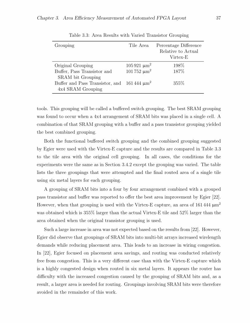
Chapter 3. Area Efficiency Measurement of Automated FPGA Layout 37
Table 3.3: Area Results with Varied Transistor Grouping
Grouping Tile Area Percentage DifferenceRelative to Actual
Virtex-E
Original Grouping 105 921 µm2 198%Buffer, Pass Transistor and 101 752 µm2 187%
SRAM bit GroupingBuffer and Pass Transistor, and 161 444 µm2 355%
4x4 SRAM Grouping
tools. This grouping will be called a buffered switch grouping. The best SRAM grouping
was found to occur when a 4x4 arrangement of SRAM bits was placed in a single cell. A
combination of that SRAM grouping with a buffer and a pass transistor grouping yielded
the best combined grouping.
Both the functional buffered switch grouping and the combined grouping suggested
by Egier were used with the Virtex-E capture and the results are compared in Table 3.3
to the tile area with the original cell grouping. In all cases, the conditions for the
experiments were the same as in Section 3.4.2 except the grouping was varied. The table
lists the three groupings that were attempted and the final routed area of a single tile
using six metal layers for each grouping.
A grouping of SRAM bits into a four by four arrangement combined with a grouped
pass transistor and buffer was reported to offer the best area improvement by Egier [22].
However, when that grouping is used with the Virtex-E capture, an area of 161 444 µm2
was obtained which is 355% larger than the actual Virtex-E tile and 52% larger than the
area obtained when the original transistor grouping is used.
Such a large increase in area was not expected based on the results from [22]. However,
Egier did observe that groupings of SRAM bits into multi-bit arrays increased wirelength
demands while reducing placement area. This leads to an increase in wiring congestion.
In [22], Egier focused on placement area savings, and routing was conducted relatively
free from congestion. This is a very different case than with the Virtex-E capture which
is a highly congested design when routed in six metal layers. It appears the router has
difficulty with the increased congestion caused by the grouping of SRAM bits and, as a
result, a larger area is needed for routing. Groupings involving SRAM bits were therefore
avoided in the remainder of this work.

Chapter 3. Area Efficiency Measurement of Automated FPGA Layout 38
Table 3.4: Area Results with Buffered Switch Grouping
Metal Layers Original Buffered Percentage DifferenceGrouping Switch Relative to Original
Grouping Grouping
6 105 921 µm2 101 752 µm2 -3.9%7 52 377 µm2 50 194 µm2 -4.2%8 43 530 µm2 39 976 µm2 -8.2%
Egier also suggested an alternate grouping of a buffer, pass transistor and SRAM
bit called a buffered switch grouping. This cell grouping does not typically lead to
increased wiring congestion since both wirelength and placement area were reduced when
this grouping was applied to the test architectures. As shown in Table 3.3, using this
grouping, the tile layout area of the Virtex-E capture was reduced to 101 752 µm2. This
is only 187% larger than the actual Virtex-E tile.
Table 3.4 shows the effect of an increased number of metal layers when this grouping
is used. An increased number of metal layers again reduces the routed area of a tile.
The tile area is only 50 194 µm2 when seven metal layers are available and 39 976 µm2
when eight metal layers are available. All these results are an area improvement over the
original grouping. The improvement ranges from an area savings of 3.9% with six metal
layers to an 8.2% reduction with eight metal layers. In all cases, the savings are less
than the 9.8% area improvement predicted by Egier’s work [22]. The reason for this is
again due to the fact that Egier performed his experimentation on relatively uncongested
designs. The congestion of the Virtex-E capture reduced the area improvements. It is
only with eight metal layers that the congestion eases and an area reduction similar to
that acheived by Egier is obtained. Regardless, this transistor grouping does reduce the
routed area and it is used for the remainder of this work.
3.4.4 Effect of Cell Bloating on Area
The best result that has been obtained for the Virtex-E capture in six metal layers
with the automated layout tools is still 187% larger than the manual design. This is
unsatisfactory since the goal of this work is to equal or improve on the results possible
with manual designs. One way to reduce the layout area may be to improve the strategy
for handling congestion. Currently, when a design is too congested for the GILES router
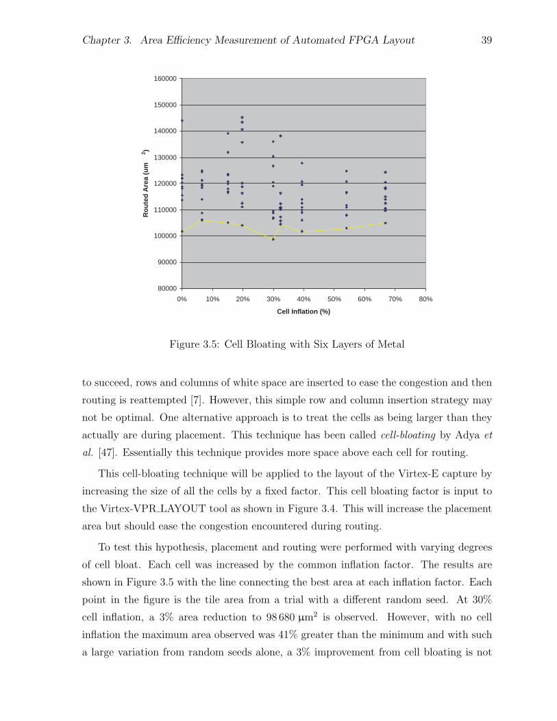
Chapter 3. Area Efficiency Measurement of Automated FPGA Layout 39
80000
90000
100000
110000
120000
130000
140000
150000
160000
0% 10% 20% 30% 40% 50% 60% 70% 80%
Cell Inflation (%)
Ro
ute
d A
rea
(um
2 )
Figure 3.5: Cell Bloating with Six Layers of Metal
to succeed, rows and columns of white space are inserted to ease the congestion and then
routing is reattempted [7]. However, this simple row and column insertion strategy may
not be optimal. One alternative approach is to treat the cells as being larger than they
actually are during placement. This technique has been called cell-bloating by Adya et
al. [47]. Essentially this technique provides more space above each cell for routing.
This cell-bloating technique will be applied to the layout of the Virtex-E capture by
increasing the size of all the cells by a fixed factor. This cell bloating factor is input to
the Virtex-VPR LAYOUT tool as shown in Figure 3.4. This will increase the placement
area but should ease the congestion encountered during routing.
To test this hypothesis, placement and routing were performed with varying degrees
of cell bloat. Each cell was increased by the common inflation factor. The results are
shown in Figure 3.5 with the line connecting the best area at each inflation factor. Each
point in the figure is the tile area from a trial with a different random seed. At 30%
cell inflation, a 3% area reduction to 98 680 µm2 is observed. However, with no cell
inflation the maximum area observed was 41% greater than the minimum and with such
a large variation from random seeds alone, a 3% improvement from cell bloating is not

Chapter 3. Area Efficiency Measurement of Automated FPGA Layout 40
significant. Another approach is needed to produce more compact layouts.
3.4.5 Effect of Metal Layer Allocation on Area
Up to this point, the allocation of the metal layers has been kept the same and all
the experiments have been performed with cells that use two metal layers for intra-
cell connections. These layers are completely un-available to the inter-cell router. Two
observations suggest this may not be optimal:
1. Many standard cell libraries use only one metal layer [48, 49]
2. The significant decrease in area observed in Sections 3.4.2 and 3.4.3 when the
number of metal layers is increased from six to seven suggests that an additional
inter-cell routing layer may be advantageous. To achieve this in a six metal layer
process, the number of layers used for intra-cell routing could be reduced.
These observations motivated the reallocation of the metal layers in the experimental
CAD flow. This affects the routing stage of the CAD flow shown in Figure 3.4 since now
there will be four layers available for inter-cell routing but only one layer for intra-cell
connections.
Before a comparable layout can be produced with one metal layer cells, the area of
these cells must be determined. Unfortunately, the area estimation model developed by
Egier in [22] was designed for two-metal layer cells and it will not correctly estimate
the area of a one metal layer cell. To address this problem, the cells required for the
Virtex-E capture were laid out by So in [50]. In Table 3.5, the area of these one metal
layer cells is compared to the two metal layer cells. The single metal layer cells require
on average 18.8% more area. An increase was expected since the layout of the cells is
more challenging when fewer metal layers are available. The impact from these cells on
the total cell area is shown in Table 3.6. In the table, active area refers to the sum of
the cell areas and it is 9.5% larger for the one layer cells relative to the two metal layer
cells. The increase in area is less than the average cell area increase because some cells
are used more frequently than others. For example, the SRAM cell is one of the most
frequently used cells and its area did not increase.
The routed tile area results using these new one metal layer cells are shown in
Figure 3.6 and summarized in Table 3.7. There is a significant reduction in area when
using the one-metal-layer cells and an extra inter-cell routing layer. When using six metal
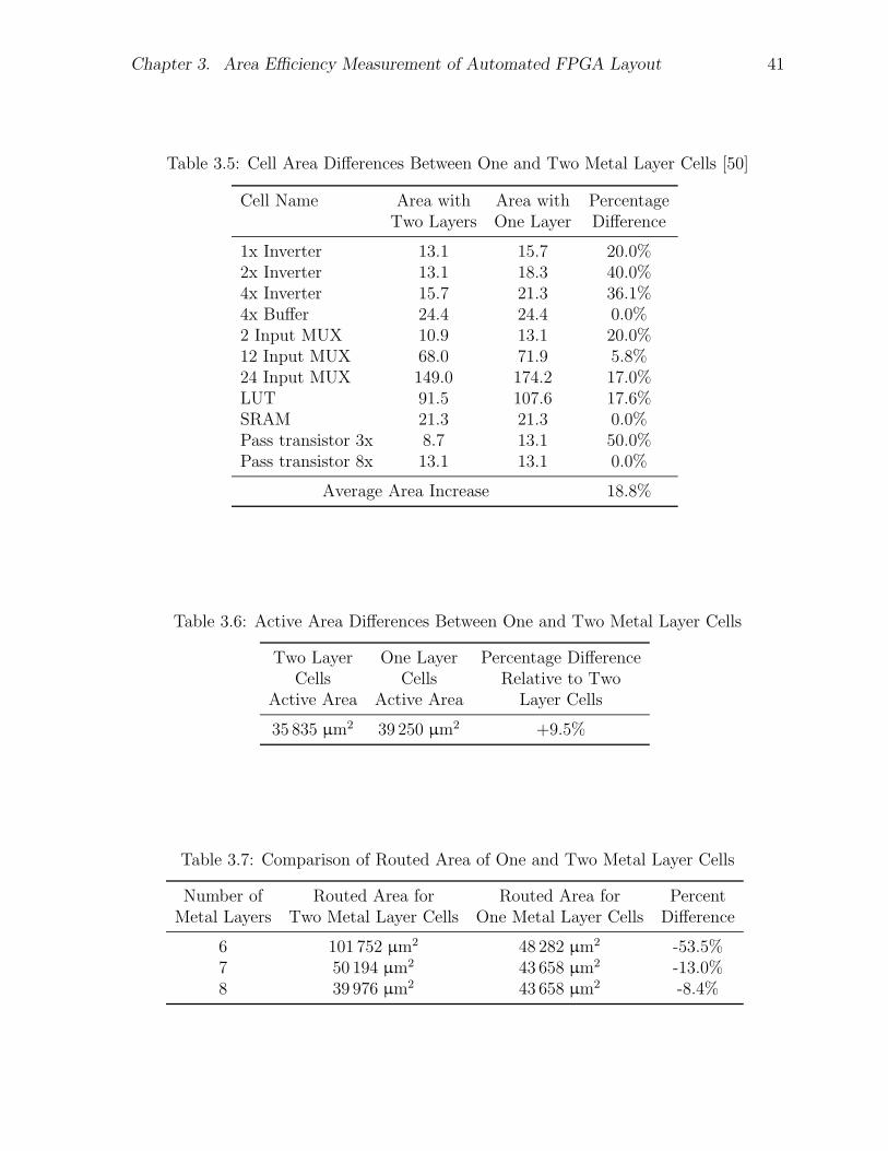
Chapter 3. Area Efficiency Measurement of Automated FPGA Layout 41
Table 3.5: Cell Area Differences Between One and Two Metal Layer Cells [50]
Cell Name Area with Area with PercentageTwo Layers One Layer Difference
1x Inverter 13.1 15.7 20.0%2x Inverter 13.1 18.3 40.0%4x Inverter 15.7 21.3 36.1%4x Buffer 24.4 24.4 0.0%2 Input MUX 10.9 13.1 20.0%12 Input MUX 68.0 71.9 5.8%24 Input MUX 149.0 174.2 17.0%LUT 91.5 107.6 17.6%SRAM 21.3 21.3 0.0%Pass transistor 3x 8.7 13.1 50.0%Pass transistor 8x 13.1 13.1 0.0%
Average Area Increase 18.8%
Table 3.6: Active Area Differences Between One and Two Metal Layer Cells
Two Layer One Layer Percentage DifferenceCells Cells Relative to Two
Active Area Active Area Layer Cells
35 835 µm2 39 250 µm2 +9.5%
Table 3.7: Comparison of Routed Area of One and Two Metal Layer Cells
Number of Routed Area for Routed Area for PercentMetal Layers Two Metal Layer Cells One Metal Layer Cells Difference
6 101 752 µm2 48 282 µm2 -53.5%7 50 194 µm2 43 658 µm2 -13.0%8 39 976 µm2 43 658 µm2 -8.4%
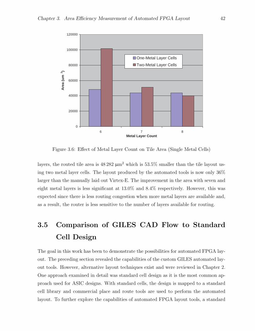
Chapter 3. Area Efficiency Measurement of Automated FPGA Layout 42
0
20000
40000
60000
80000
100000
120000
6 7 8Metal Layer Count
Are
a (u
m2 )
One-Metal Layer Cells
Two-Metal Layer Cells
Figure 3.6: Effect of Metal Layer Count on Tile Area (Single Metal Cells)
layers, the routed tile area is 48 282 µm2 which is 53.5% smaller than the tile layout us-
ing two metal layer cells. The layout produced by the automated tools is now only 36%
larger than the manually laid out Virtex-E. The improvement in the area with seven and
eight metal layers is less significant at 13.0% and 8.4% respectively. However, this was
expected since there is less routing congestion when more metal layers are available and,
as a result, the router is less sensitive to the number of layers available for routing.
3.5 Comparison of GILES CAD Flow to Standard
Cell Design
The goal in this work has been to demonstrate the possibilities for automated FPGA lay-
out. The preceding section revealed the capabilities of the custom GILES automated lay-
out tools. However, alternative layout techniques exist and were reviewed in Chapter 2.
One approach examined in detail was standard cell design as it is the most common ap-
proach used for ASIC designs. With standard cells, the design is mapped to a standard
cell library and commercial place and route tools are used to perform the automated
layout. To further explore the capabilities of automated FPGA layout tools, a standard

Chapter 3. Area Efficiency Measurement of Automated FPGA Layout 43
cell layout is now compared to one produced using the GILES layout tools.
3.5.1 Methodology
For this experiment, the netlist generator, Virtex-VPR LAYOUT, was modified to pro-
duce a Verilog netlist of standard cells instead of the custom cells used previously. Cells
such as large multiplexers, which are treated as a single cell in the conventional CAD
flow when using the GILES layout tools, were mapped to multiple two-input multiplex-
ers. The Diplomat-18 Standard Cell Library from Virtual Silicon Technology [36] made
available to the University of Toronto through the Canadian Microelectronics Corpora-
tion (CMC) [51] was used. Since pass transistor and SRAM cells are not available in this
library, these cells were manually laid out using the circuitry as given in [8].
The Verilog netlist was imported into Cadence Design Planner and Cadence Silicon
Ensemble [37, 38]. Placement was performed using Cadence’s QPlace engine and Ca-
dence’s WRoute was used for global and detailed routing. As with GILES, the entire
process was not timing driven. This ensures a fair comparison even though the commer-
cial packages can accept timing constraints.
The commercial tools used were not designed for the creation of FPGA tiles and
hence do not consider issues such as ensuring that ports from a tile connect in a pattern
that allows multiple-tile length wires to be realized. To make a fair comparison with the
tile-based approach, instead of a single tile, a 4x4 array of tiles was placed and routed.
This eliminates the need for ports to describe the relationship between tiles. To compare
results with GILES, the total area and wire lengths obtained from the commercial tools
are divided by the number of tiles to produce a per tile value.
3.5.2 Comparison Qualifications/Caveats
The goal in this comparison is to approximately compare the tile area of a layout produced
using the GILES tools and a standard cell layout. As a result, some simplifications were
made when generating the standard cell design. These simplifications and their area
impact is as follows:
1. The issue of buffer sizing was not reevaluated and instead a single size of buffers
was used in all cases. This assumption will underestimate the standard cell area if
stronger buffers are required to minimize the area delay product. It is also possible
Chapter 3. Area Efficiency Measurement of Automated FPGA Layout 44
that some standard cells have greater drive strengths than required. In that case
the area of the standard cell implementation will be overestimated.
2. The mapping of large multiplexers into collections of connected two-input multi-
plexers is not optimal and likely increases the area required for the standard cell
layout.
3. The standard cell implementation does not allow for port constraints. As discussed
previously, this problem is resolved by placing and routing a large array of tiles.
With this larger array, the challenge of placing and routing the design is more
complex. However, there is also the possibility for additional optimizations that
are not possible when using the GILES layout tools since they operate only on a
single tile.
4. The tiles at the edge of the standard cell implementation do not connect to pad cells
so the wirelength needs of the standard cell implementation are somewhat reduced
compared to layout produced with the GILES automated layout tools since, with
the GILES layout tools, wires to which connections must be made are always routed
to the edge of the tile.
5. A multitude of factors, such as input settings for row utilization and aspect ratio,
influence the placement and routing of a standard cell design. This standard cell
implementation was produced targeting an aspect ratio of 1.0 and a row utilization
of 85 %. Since an extensive examination of the possible input parameters was not
conducted, a smaller standard cell design may be possible.
3.5.3 Results
The results of the comparison between a standard cell layout and one produced using
the GILES layout tools are summarized in Table 3.8. The column in the table labelled
“GILES-Generated Tile” gives the area result from Section 3.4.5 using a six metal layer
process. That was the best area achieved using six layers and it was obtained following
the procedure of Section 3.4.1 which is entirely based on the GILES tools. Comparing
final tile areas, the standard cell tile is 48% larger having an area of 71 569 µm2 compared
to the GILES-generated tile with its area of 48 282 µm2.
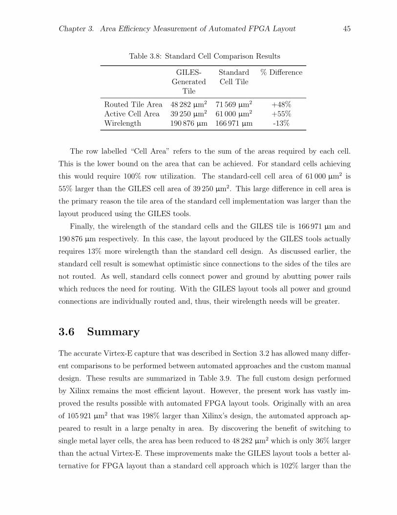
Chapter 3. Area Efficiency Measurement of Automated FPGA Layout 45
Table 3.8: Standard Cell Comparison Results
GILES- Standard % DifferenceGenerated Cell Tile
Tile
Routed Tile Area 48 282 µm2 71 569 µm2 +48%Active Cell Area 39 250 µm2 61 000 µm2 +55%Wirelength 190 876 µm 166 971 µm -13%
The row labelled “Cell Area” refers to the sum of the areas required by each cell.
This is the lower bound on the area that can be achieved. For standard cells achieving
this would require 100% row utilization. The standard-cell cell area of 61 000 µm2 is
55% larger than the GILES cell area of 39 250 µm2. This large difference in cell area is
the primary reason the tile area of the standard cell implementation was larger than the
layout produced using the GILES tools.
Finally, the wirelength of the standard cells and the GILES tile is 166 971 µm and
190 876 µm respectively. In this case, the layout produced by the GILES tools actually
requires 13% more wirelength than the standard cell design. As discussed earlier, the
standard cell result is somewhat optimistic since connections to the sides of the tiles are
not routed. As well, standard cells connect power and ground by abutting power rails
which reduces the need for routing. With the GILES layout tools all power and ground
connections are individually routed and, thus, their wirelength needs will be greater.
3.6 Summary
The accurate Virtex-E capture that was described in Section 3.2 has allowed many differ-
ent comparisons to be performed between automated approaches and the custom manual
design. These results are summarized in Table 3.9. The full custom design performed
by Xilinx remains the most efficient layout. However, the present work has vastly im-
proved the results possible with automated FPGA layout tools. Originally with an area
of 105 921 µm2 that was 198% larger than Xilinx’s design, the automated approach ap-
peared to result in a large penalty in area. By discovering the benefit of switching to
single metal layer cells, the area has been reduced to 48 282 µm2 which is only 36% larger
than the actual Virtex-E. These improvements make the GILES layout tools a better al-
ternative for FPGA layout than a standard cell approach which is 102% larger than the
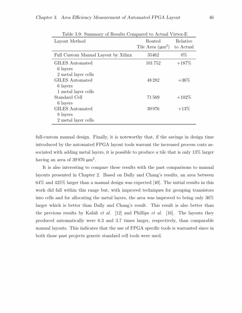
Chapter 3. Area Efficiency Measurement of Automated FPGA Layout 46
Table 3.9: Summary of Results Compared to Actual Virtex-E
Layout Method Routed RelativeTile Area (µm2) to Actual
Full Custom Manual Layout by Xilinx 35462 0%
GILES Automated 101 752 +187%6 layers2 metal layer cells
GILES Automated 48 282 +36%6 layers1 metal layer cells
Standard Cell 71 569 +102%6 layers
GILES Automated 39 976 +13%8 layers2 metal layer cells
full-custom manual design. Finally, it is noteworthy that, if the savings in design time
introduced by the automated FPGA layout tools warrant the increased process costs as-
sociated with adding metal layers, it is possible to produce a tile that is only 13% larger
having an area of 39 976 µm2.
It is also interesting to compare these results with the past comparisons to manual
layouts presented in Chapter 2. Based on Dally and Chang’s results, an area between
64% and 425% larger than a manual design was expected [40]. The initial results in this
work did fall within this range but, with improved techniques for grouping transistors
into cells and for allocating the metal layers, the area was improved to being only 36%
larger which is better than Dally and Chang’s result. This result is also better than
the previous results by Kafafi et al. [12] and Phillips et al. [16]. The layouts they
produced automatically were 6.3 and 3.7 times larger, respectively, than comparable
manual layouts. This indicates that the use of FPGA specific tools is warranted since in
both those past projects generic standard cell tools were used.
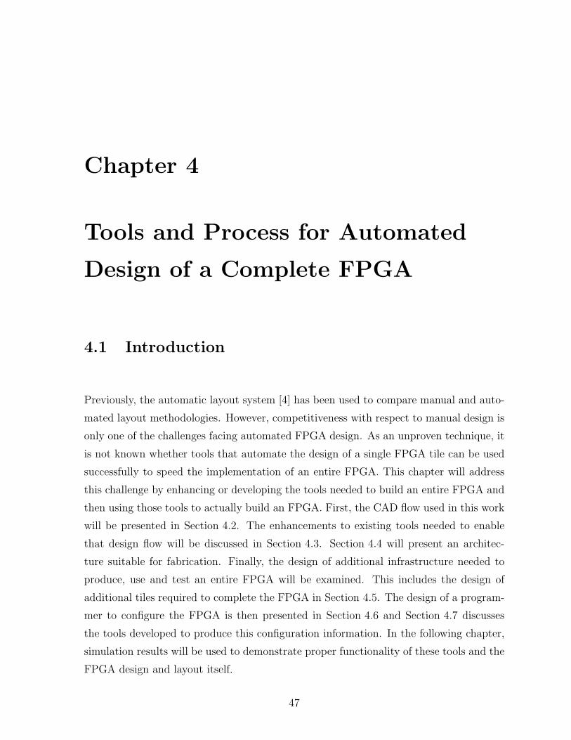
Chapter 4
Tools and Process for Automated
Design of a Complete FPGA
4.1 Introduction
Previously, the automatic layout system [4] has been used to compare manual and auto-
mated layout methodologies. However, competitiveness with respect to manual design is
only one of the challenges facing automated FPGA design. As an unproven technique, it
is not known whether tools that automate the design of a single FPGA tile can be used
successfully to speed the implementation of an entire FPGA. This chapter will address
this challenge by enhancing or developing the tools needed to build an entire FPGA and
then using those tools to actually build an FPGA. First, the CAD flow used in this work
will be presented in Section 4.2. The enhancements to existing tools needed to enable
that design flow will be discussed in Section 4.3. Section 4.4 will present an architec-
ture suitable for fabrication. Finally, the design of additional infrastructure needed to
produce, use and test an entire FPGA will be examined. This includes the design of
additional tiles required to complete the FPGA in Section 4.5. The design of a program-
mer to configure the FPGA is then presented in Section 4.6 and Section 4.7 discusses
the tools developed to produce this configuration information. In the following chapter,
simulation results will be used to demonstrate proper functionality of these tools and the
FPGA design and layout itself.
47
Chapter 4. Tools and Process for Automated Design of a Complete FPGA 48
Packing - T-VPACK
Place andRoute - VPR
BitstreamGeneration -VPRLAYOUT
Circuit
Description
- BLIF
Bitstream
Netlist ofLayouts
ArchitectureDescription
Figure 4.1: CAD Flow
4.2 CAD Flow
Prior to describing the design and construction of an FPGA, it is necessary to consider
how this FPGA will be used. The GILES layout system automates the design process
from architecture description to layout. This however, is only half the problem as the
physical layout is simply an implementation of an FPGA suitable for fabrication in
silicon. To test and use this FPGA, one must be able to program the device with
actual designs. These circuits must be implemented on the FPGA by configuring all
the programmable elements in the FPGA. This programming information is typically
referred to as a bitstream. The task of generating this bitstream is far too arduous a
task to be performed manually and, hence, a CAD flow was developed to facilitate this
process.
This CAD flow is shown in Figure 4.1. The main input to the tools is a Berkeley
Logic Interchange Format (BLIF) [52] file describing the circuit to be implemented in
terms of the LUTs and flip flops present in the FPGA and the output is a bitstream that
configures the FPGA appropriately. The first step in creating the bitstream involves
using T-VPack [53] for packing groups of FPGA components into larger logic blocks.
T-VPack also requires an architecture description to define the logic blocks that are
Chapter 4. Tools and Process for Automated Design of a Complete FPGA 49
available. Once the packing is complete, the VPR Placer [19] is used to determine
where on the FPGA the logic blocks will be positioned. The VPR Router [19] then
connects the placed components as specified in the netlist. The FPGA architecture used
by the placer and router is defined in an architecture description input to these tools.
Finally, the bitstream generator translates the placed and routed design into a bitstream
of configuration bits that can be used to program the FPGA. This step depends on the
physical implementation of the FPGA and therefore, the netlists describing the FPGA
tiles must be provided as inputs as well.
4.3 Tool Enhancements to Support Bitstream Gen-
eration
The CAD flow presented in the preceding section relies on tools that were developed for
prior work. T-VPack was created by Marquardt in [53] and Betz developed VPR as part
of his work in [19]. The CAD flow for this work requires a bitstream as its end product
but, unfortunately, the past work that created T-VPack and VPR did not have this goal
in mind. As a result, some enhancements to these tools are required to integrate them
with a bitstream-oriented CAD flow.
4.3.1 T-VPack for Bitstream Generation
To support bitstream generation, the tool for the first stage in the CAD flow, packing,
was updated. The primary deficiency with the original T-VPack was the lack of LUT
configuration information. When actually using an FPGA, the LUT must be configured
to implement a specific boolean function. This is done by setting the SRAM bits which
connect to the LUT. The configuration of these bits is frequently referred to as the LUT
mask. T-VPack was not designed for bitstream generation and, hence, it discards this
information about the LUT configuration.
To remedy this problem, this work first enhanced T-VPack to read in the information
about the LUT configuration from the input BLIF file. A BLIF file describes the circuit
in a verbose truth table format and the enhanced T-VPack maps this truth table to a
numerical representation. This gives each LUT a numerical value that will later be used
to generate the LUT mask.
Chapter 4. Tools and Process for Automated Design of a Complete FPGA 50
The BLIF definition does allow for various configurations of the flip-flops or latches
in the circuit. Falling or rising edge sensitive flip flops or active high or low latches can
be specified. The target FPGA that will be created with the GILES tools does not have
this flexibility and, hence, this information will be ignored. Rising edge sensitive flip
flops will be assumed and no additional enhancements were added to support flip flop
configuration information.
The added LUT mask information does pose a problem since the T-VPack output, a
VPR-style netlist, does not have the capability to store the additional information. To
accommodate this information, the VPR-style netlist format was extended. For com-
patibility with the original version of VPR, this was done by embedding the numerical
LUT representation in the comments. The original format specified comments using a
’#’. Now in the updated version, if the comment symbol is immediately proceeded by an
exclamation point as in ’#!’ the comment symbol will be ignored. With this approach,
this updated version of T-VPack will function with all versions of VPR.
4.3.2 Bitstream Generation within VPR
VPR also requires enhancements to perform bitstream generation. It too, like T-VPack,
ignored LUT information and, thus, it was first enhanced to read in the improved netlist
containing the LUT configuration. This information is then saved for later use by the
bitstream generator. This resolves the problem of having insufficient information to
configure the FPGA.
Architecture Generation
Another issue arises in ensuring that the architecture generated by the VPR Architecture
Generator matches the layout that will be generated with the GILES layout system. As
discussed in Section 2.5, the automatic layout system creates a single tile that is replicated
to form a larger array of routing and logic clusters. This places some restrictions, such as
track count, on the possible architectures that can be constructed. These restrictions have
been discussed in Section 2.5.1 and [5]. However, that discussion focused only on ensuring
that the architecture description input to VPR was suitable for tiling. Other issues exist
in how that architecture description is implemented by the Architecture Generator. The
generator must produce an internal structure that exactly matches the structure created
by the replicated tile layouts. An architecture that meets these constraints will be referred
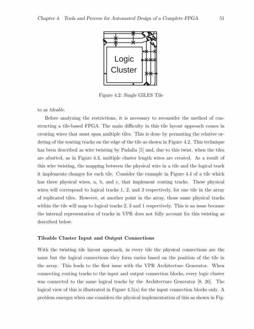
Chapter 4. Tools and Process for Automated Design of a Complete FPGA 51
LogicCluster
Figure 4.2: Single GILES Tile
to as tileable.
Before analyzing the restrictions, it is necessary to reconsider the method of con-
structing a tile-based FPGA. The main difficulty in this tile layout approach comes in
creating wires that must span multiple tiles. This is done by permuting the relative or-
dering of the routing tracks on the edge of the tile as shown in Figure 4.2. This technique
has been described as wire twisting by Padalia [5] and, due to this twist, when the tiles
are abutted, as in Figure 4.3, multiple cluster length wires are created. As a result of
this wire twisting, the mapping between the physical wire in a tile and the logical track
it implements changes for each tile. Consider the example in Figure 4.4 of a tile which
has three physical wires, a, b, and c, that implement routing tracks. These physical
wires will correspond to logical tracks 1, 2, and 3 respectively, for one tile in the array
of replicated tiles. However, at another point in the array, those same physical tracks
within the tile will map to logical tracks 2, 3 and 1 respectively. This is an issue because
the internal representation of tracks in VPR does not fully account for this twisting as
described below.
Tileable Cluster Input and Output Connections
With the twisting tile layout approach, in every tile the physical connections are the
same but the logical connections they form varies based on the position of the tile in
the array. This leads to the first issue with the VPR Architecture Generator. When
connecting routing tracks to the input and output connection blocks, every logic cluster
was connected to the same logical tracks by the Architecture Generator [8, 20]. The
logical view of this is illustrated in Figure 4.5(a) for the input connection blocks only. A
problem emerges when one considers the physical implementation of this as shown in Fig-
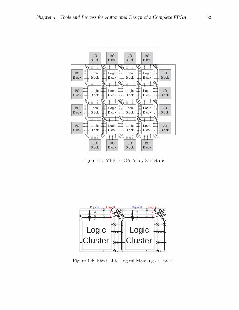
Chapter 4. Tools and Process for Automated Design of a Complete FPGA 52
LogicBlock
LogicBlock
LogicBlock
LogicBlock
LogicBlock
LogicBlock
LogicBlock
LogicBlock
LogicBlock
LogicBlock
LogicBlock
LogicBlock
LogicBlock
LogicBlock
LogicBlock
I/OBlock
I/OBlock
I/OBlock
I/OBlock
I/OBlock
I/OBlock
I/OBlock
I/OBlock
I/OBlock
I/OBlock
I/OBlock
I/OBlock
I/OBlock
I/OBlock
I/OBlock
I/OBlock
LogicBlock
Figure 4.3: VPR FPGA Array Structure
LogicCluster
LogicCluster
abc
abc
Physical Physical
123
Logical
231
Logical
Figure 4.4: Physical to Logical Mapping of Tracks
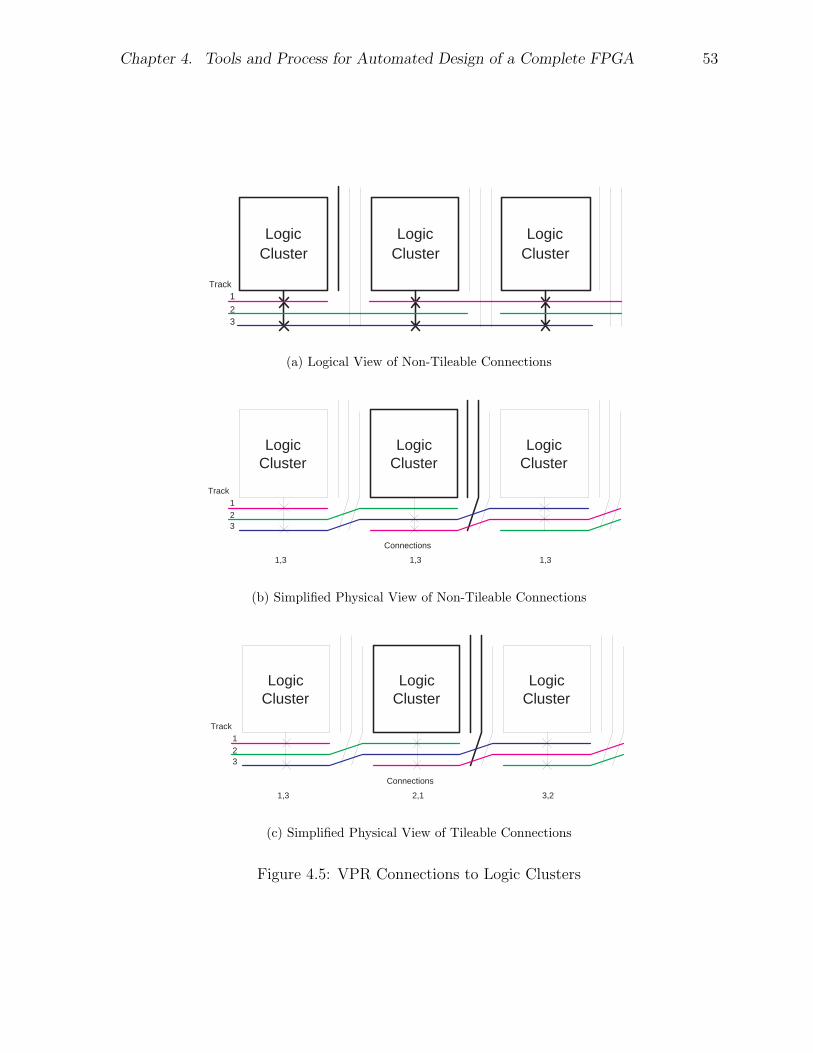
Chapter 4. Tools and Process for Automated Design of a Complete FPGA 53
LogicCluster
LogicCluster
LogicCluster
1
23
Track
(a) Logical View of Non-Tileable Connections
LogicCluster
LogicCluster
LogicCluster
123
1,3 1,3 1,3
Track
Connections
(b) Simplified Physical View of Non-Tileable Connections
LogicCluster
LogicCluster
LogicCluster
123
1,3 2,1 3,2
Track
Connections
(c) Simplified Physical View of Tileable Connections
Figure 4.5: VPR Connections to Logic Clusters
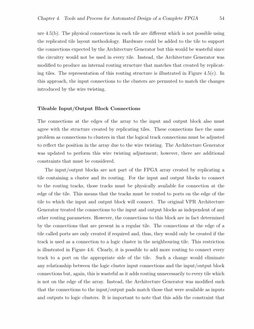
Chapter 4. Tools and Process for Automated Design of a Complete FPGA 54
ure 4.5(b). The physical connections in each tile are different which is not possible using
the replicated tile layout methodology. Hardware could be added to the tile to support
the connections expected by the Architecture Generator but this would be wasteful since
the circuitry would not be used in every tile. Instead, the Architecture Generator was
modified to produce an internal routing structure that matches that created by replicat-
ing tiles. The representation of this routing structure is illustrated in Figure 4.5(c). In
this approach, the input connections to the clusters are permuted to match the changes
introduced by the wire twisting.
Tileable Input/Output Block Connections
The connections at the edges of the array to the input and output block also must
agree with the structure created by replicating tiles. These connections face the same
problem as connections to clusters in that the logical track connections must be adjusted
to reflect the position in the array due to the wire twisting. The Architecture Generator
was updated to perform this wire twisting adjustment; however, there are additional
constraints that must be considered.
The input/output blocks are not part of the FPGA array created by replicating a
tile containing a cluster and its routing. For the input and output blocks to connect
to the routing tracks, those tracks must be physically available for connection at the
edge of the tile. This means that the tracks must be routed to ports on the edge of the
tile to which the input and output block will connect. The original VPR Architecture
Generator treated the connections to the input and output blocks as independent of any
other routing parameters. However, the connections to this block are in fact determined
by the connections that are present in a regular tile. The connections at the edge of a
tile called ports are only created if required and, thus, they would only be created if the
track is used as a connection to a logic cluster in the neighbouring tile. This restriction
is illustrated in Figure 4.6. Clearly, it is possible to add more routing to connect every
track to a port on the appropriate side of the tile. Such a change would eliminate
any relationship between the logic cluster input connections and the input/output block
connections but, again, this is wasteful as it adds routing unnecessarily to every tile which
is not on the edge of the array. Instead, the Architecture Generator was modified such
that the connections to the input/output pads match those that were available as inputs
and outputs to logic clusters. It is important to note that this adds the constraint that

Chapter 4. Tools and Process for Automated Design of a Complete FPGA 55
Input/OutputPad
LogicCluster
Connections Must Match
LogicCluster
FPGA Tiles
Input/Output Blocks
Tile Boundary
Tile Boundary
Figure 4.6: Restrictions on Input and Output Pin Connections
the number of input and output connection tracks to a cluster must match the number
to the input/output blocks.
4.4 Architecture Decisions
Given the goal in this work of proving the viability of automatic FPGA generation,
a specific architecture for the FPGA to be fabricated must be selected. The goal in
producing this FPGA is not to generate a replica of a commercial device. This contrasts
the goal of Chapter 3 which aimed to replicate a commercial device with reasonable
accuracy. Producing an FPGA comparable to such a commercial device is not feasible, as
it would require the development of a new FPGA CAD flow since the CAD flow outlined
in Section 4.2 can not handle modern commercial devices. Such an effort is well beyond
the scope of this work. Furthermore, it is unnecessary to achieve this work’s primary goal
of proving the viability of automated FPGA layout. Instead, an architecture that can
be generated by VPR will be selected. This approach demonstrates the capabilities of
automated FPGA design as the architectures that VPR can handle are not significantly
less complex than a commercial FPGA from a layout and circuit design perspective.
Other considerations, besides the constraints imposed by the VPR Architecture Gen-
Chapter 4. Tools and Process for Automated Design of a Complete FPGA 56
erator and the tileablility restrictions discussed in Section 4.3, must also be taken into
account. The most significant issue is silicon availability. The architecture must be cho-
sen such that a tile will be sufficiently small that an interesting number of tiles can be
created on the amount of silicon available in an academic environment. The process of
selecting such an architecture will now be given.
4.4.1 Logic Block Parameters
Given the prevalence of four-input LUTs in academic and commercial work [24, 25, 54, 55]
it is appropriate to use them in this work as well. Past work such as that by Ahmed
et al. in [56] has also revealed that 4-LUTs deliver the best area results. The selection
of 4-LUTs also allows the results from past architectural examinations to be directly
applied, which simplifies the architectural decisions made for this design.
The next most important parameter influencing tile area is cluster size since, in a
properly designed architecture, this will impact other crucial factors such as track count.
The issue of cluster size has been extensively studied in the past by Betz et al. in [8]
and Ahmed et al. in [56]. Based on those results, a cluster size of one was rejected
since it offers poor speed performance. Increasing the cluster size to two results in a
significant area efficiency penalty as local routing, which makes connections within the
cluster, requires more area to create than the general routing area reduction it provides.
Hence, a cluster size of three was selected. While larger clusters may offer slight area
efficiency gains, the desire to minimize the size of the logic blocks to create the largest
array possible necessitates selecting the cluster size of three.
In [8], Betz et al. developed the following empirical relationship to determine the
number of inputs, I, required to effectively use a given cluster size, N.
I = 2N + 2 (4.1)
With a cluster size of, N = 3, this gives 8 inputs per cluster. The architectures generated
by VPR assume that every BLE has a single output and, thus, each logic cluster will also
have three outputs.
Each cluster output need not connect to every track. The fraction of tracks to which
any given output connects, denoted Fc,output, was experimentally found in [8] to be suffi-
ciently flexible when set to 1/N. Thus, a value of 1/3 is appropriate for this design.
Chapter 4. Tools and Process for Automated Design of a Complete FPGA 57
4.4.2 Routing Structure
To simplify the design of this FPGA, a single type of routing track will be used. Un-
buffered pass transistors, while small in area, make electrical design more challenging as
multi-segment routes face significant resistive load. Thus, to mitigate any such potential
problems, a fully buffered routing architecture will be used. This means that tristate
buffers will be used for all the routing switches.
Given this all-buffered routing network, tracks of length four will be used. Betz et
al. in [8] found that, when a single length of routing is used, a length of four or eight is
optimum. Since this FPGA will not consist of a large array, selecting length four wires is
more appropriate. The results in [8] were for a different cluster size and, thus, may not
be directly applicable to a cluster size of three. However, it is unlikely that their area
efficiency would be significantly degraded in the current architecture since the cluster
size is only one less than was used by Betz et al. [8].
4.4.3 Array Size
Each tile is replicated to form an array of tiles. The dimensions of this array, nx x ny,
can be of any size. However, given the length four routing architecture, constructing
an array of less than 4 x 4 would not be interesting as no track would realize its full
length. Thus, an array size of 8 x 8 was selected since it allows two full length wires to
be realized. Based on the packages that will be available for the final fabricated device,
it was decided that two input/output pins would be connected per logic block row and
column. A lower value would severely limit the number of implementable circuits while
a higher value would require more advanced packaging.
With this array size there will be 8 × 8 × 3 = 192 4-LUTs and 8 × 4 × 2 = 64
programmable input/output pins in the design. This is relatively small compared to a
more current device family such as the Xilinx Virtex-E with devices ranging in size from
1532 4-LUTs to 64896 4-LUTs and 176 to 804 user I/O pins [24]. Such a comparably small
size does not make this design less relevant or viable as other recent designs such as the
MAX II Complex Programmable Logic Device (CPLD) family are only marginally larger
with between 240 and 2210 4-LUTs and 80 to 272 I/O pins [57]. It is also interesting
to observe that the device to be created in this work will be larger than one of the first
FPGAs ever produced commercially, the Xilinx 2064 which contained only 64 4-LUTs
[58].
Chapter 4. Tools and Process for Automated Design of a Complete FPGA 58
4.4.4 Track Count
The number of tracks has a significant impact on the routability of the FPGA. The
following equation offers an estimate of the required average track width, Waverage [3, 59]:
Waverage =λR
2
where λ is the number of pins connected to each logic block and R is the average length
of wires in the channel. With an average length of R = 3 [3] and λ = 11 total pins, this
gives an average track width of 16.5 tracks. This however is only an average and the
FPGA must be designed to handle cases that are worse than average. Thus, instead of
using an analytical expression to determine the number of tracks that the architecture
should have, it will be determined experimentally.
Methodology
To find a suitable number of tracks for this architecture, a set of benchmark circuits will
be placed and routed on the FPGA fabric. The ability to route these circuits will be
observed and examined in conjunction with the area required for the architecture. The
goal will be to find the number of tracks needed to allow for easy routing while keeping
the tile area as small as possible.
The CAD flow discussed in Section 4.2 was used for this investigation. A set of MCNC
circuits [60] that have already been synthesized were used for testing. Appendix A lists
the properties of these circuits. The packing tool, T-VPack [53], was configured for a
cluster size of three with eight inputs but was otherwise left with default settings. Place-
ment and routing were then performed using VPR. The input architecture description
to VPR was based on the parameters determined in the preceding sections. For Fc,input
which will be determined in Section 4.4.5, a value of 0.5 will be used. Later experimen-
tation will determine if this is acceptable. To ease routing congestion in the periphery
and focus on the number of tracks required in the core of the FPGA array Fc,pad was
set to 1.0. The number of routing tracks was varied with the constraint, as discussed
in Section 2.5.1, that the track count must be a multiple of the track length which in
this case is four. This procedure was repeated ten times to reduce the influence of noise
from the simulated annealing-based placer. A circuit was considered to have routed if it
succeeded on any of these trials.
Chapter 4. Tools and Process for Automated Design of a Complete FPGA 59
To determine the circuit area for each given track count, the GILES layout system was
used following the procedure from Section 2.5. The architecture description is input to
VPR LAYOUT which generates a netlist that is placed and routed by the GILES placer
and router respectively. Actual cell layouts were not available; instead, the area model
for two metal layer cells developed by Egier in [22] was used. A six metal layer process
was assumed. One metal layer was allocated for global power and ground distribution
which leaves three layers for inter-cell routing. This process was repeated using the same
number of tracks per channel as the place and route tests with VPR. The trials will be
compared in terms of the final routed area for a single tile.
Results
The data from the above experiment is plotted in Figure 4.7. The tile area, shown in
Figure 4.7(a), increases approximately linearly with an increasing number of tracks. The
number of successfully routable circuits, shown in Figure 4.7(b), also increases initially
with the track count but it plateaus once there are 20 tracks in each channel. At this
point, all the circuits that can fit on an FPGA of this size are being routed successfully.
Given the increasing tile area, the minimum number of tracks that satisfy the routing
requirements will be selected. Accordingly, it was decided that the architecture will have
twenty tracks per channel.
4.4.5 Connection Block Flexibility
Finally, the fraction of tracks that connect to each cluster input, Fc,input, must be deter-
mined. Betz et al. [8] suggests a value higher than Fc,output and, thus, in the previous
experiments a value of 0.5 was selected. However, as described in Section 4.3.2, it was
discovered that in a tileable architecture a relationship exists between Fc,input and Fc,pad
where Fc,pad is the fraction of tracks to which an input or output pad pin connects. The
experimentation in Section 4.4.4 ignored this effect so as to focus exclusively on routing
concerns related to the track count. Thus, it is necessary to conduct further testing in
which Fc,input is set equal to Fc,pad.
Methodology
The same process as used in Section 4.4.4 was used to determine an appropriate connec-
tion block flexibility. The same MCNC benchmark circuits [60] were used in conjunction

Chapter 4. Tools and Process for Automated Design of a Complete FPGA 60
0
5000
10000
15000
20000
25000
30000
35000
40000
0 5 10 15 20 25 30 35 40 45 50
Number of Tracks per Channel
Tile
Are
a (u
m2)
(a)
0
20
40
60
80
100
120
140
0 5 10 15 20 25 30 35 40 45 50
Number of Tracks per Channel
Nu
mb
er o
f S
ucc
essf
ully
Ro
ute
d C
ircu
its
(b)
Figure 4.7: Area and Number of Routable Circuits over Varied Track Widths

Chapter 4. Tools and Process for Automated Design of a Complete FPGA 61
with T-VPack and VPR for packing, placement and routing. Placement and routing
were performed using ten different placement seeds. In this case, however, Fc,input was
varied while the number of tracks was held constant at twenty. To address tileability
issues Fc,pad was kept equal to Fc,input. These flexibilities will be reported as the fraction
of tracks the connection block connects to relative to the total number of tracks. This
flexibility will then be varied between 0.05 and 1 representing between 1 and 20 input
tracks. As was done previously, the GILES layout tools will be used to determine the
tile area of the architecture at each specific connection box flexibility.
Results
The results from this experimentation are plotted in Figure 4.8. With respect to the
connection block flexibility, the tile area again increases approximately linearly. However,
the slope of this increase is significantly less and the area only increases by 5 450 µm2
over the range of Fc,input. The number of routable circuits does plateau again but prior to
this plateau there is significant variation in number of routable circuits. Isolated Fc,input
values such as 0.45 appear to provide excellent routability while a larger Fc,input value of
0.5 is significantly more challenging for routing. This is an interesting phenomenon since
an increased flexibility is typically expected to provide easier routing. The reason for this
is likely due to the technique used for selecting the specific input tracks for each cluster
input. Improving this technique may allow for more consistent routability results but is
beyond the scope of this work. For this design, a value of 0.6 was selected since it is in
a region in which circuits are consistently routable. Selecting a lower value could offer a
slight area reduction but would not reliably increase the ease of routing. Therefore, the
Fc,input value of 0.6 was considered the most appropriate.
4.4.6 Summary of Architecture
The most significant architecture parameters discussed above are summarized in Table 4.1.
4.5 Periphery Design
Previous work [5, 4, 6, 7] with the GILES automatic layout system has focused on the
layout of a single tile containing a single logic cluster and its associated routing as shown
previously in Figure 4.2. This tile can then be used to create arbitrary sized arrays
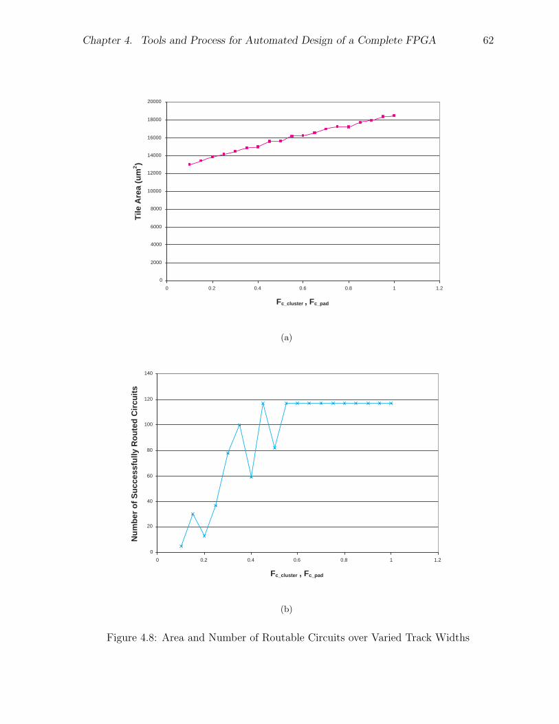
Chapter 4. Tools and Process for Automated Design of a Complete FPGA 62
0
2000
4000
6000
8000
10000
12000
14000
16000
18000
20000
0 0.2 0.4 0.6 0.8 1 1.2
Fc_cluster , Fc_pad
Tile
Are
a (u
m2)
(a)
0
20
40
60
80
100
120
140
0 0.2 0.4 0.6 0.8 1 1.2
Fc_cluster , Fc_pad
Nu
mb
er o
f S
ucc
essf
ully
Ro
ute
d C
ircu
its
(b)
Figure 4.8: Area and Number of Routable Circuits over Varied Track Widths

Chapter 4. Tools and Process for Automated Design of a Complete FPGA 63
Table 4.1: Architecture Parameters
Parameter Value
LUT Size, k 4Cluster Size, N 3Number of Cluster Inputs, I 8Track Width, W 20Track Length, L 4% Buffered Tracks 100%Fc,input 0.6Fc,output 0.333Fc,pad 0.6Array Size, nx x ny 8 x 8Pads per column 2
Total Number of LUTs 192Total Number of I/O’s 64
of logic clusters. However, examination of the entire FPGA design assumed by VPR
illustrated in Figure 4.3, reveals that the single tile does not capture all of the assumed
functionality at the periphery of the FPGA array. Most noticeably, the I/O blocks at
the edge of the FPGA array, which are needed to connect tracks as inputs and outputs,
are not included in the main tile. The VPR Architecture Generator also assumes that
there are additional routing channels at the bottom and left sides of the FPGA array.
Since the main tile only captures the routing channels above and to the right of the logic
block, these additional channel will not be created by simple tiling of the primary tile.
There are numerous possible methods to remedy this discrepancy between the VPR
structure and that generated by the GILES tools. Since this is only at the edge of the
array, manual implementation of the additional routing elements is feasible but does not
fit with the automatic design goals of this project. An alternative is to alter the VPR
Architecture Generator such that its structure matches that of automatic layout. This,
however, only solves the problem regarding the additional routing channels as I/O blocks
are still needed for connecting inputs and outputs. The approach that was decided upon
was to augment the automatic layout system to produce additional tiles containing the
required functionality.
A total of seven additional tiles are needed. One additional tile is needed on each side
of the array and three corner tiles are needed. The routing network alone only requires
one corner tile; the other two corners are needed for programming infrastructure as will

Chapter 4. Tools and Process for Automated Design of a Complete FPGA 64
Main Tile
Main Tile
Main Tile
Main Tile
Main Tile
Main Tile
Main Tile
Main Tile
Main Tile
BottomTile
BottomTile
BottomTile
Top Tile Top Tile Top Tile
Left Tile
Left Tile
Left Tile
CornerBottomLeft Tile
CornerTop Left
Tile
Right Tile
Right Tile
Right Tile
CornerBottom
Right Tile
Programmer
I/O Pad I/O Pad I/O Pad
I/O Pad
I/O Pad
I/O Pad
I/O Pad I/O Pad I/O Pad
I/O Pad
I/O Pad
I/O Pad
InputPads
Figure 4.9: FPGA Floor plan with Periphery Tiles
be discussed in Section 4.6. The top right corner position is empty. This floor plan of all
the tiles is shown for a 3 x 3 array in Figure 4.9. The 8 x 8 array created in this work
will have the same structure.
4.5.1 Periphery Generation
The periphery tiles must be generated in a multi-step process. The main tile is first gener-
ated using the normal automated layout approach with GILES in which VPR LAYOUT
translates VPR’s routing resource graph into a netlist suitable for the GILES Placer and
Router. Once this tile is placed and routed, it must be processed by VPR LAYOUT to
produce the edge tiles (Bottom, Left, Top and Right). This must occur after the main
tile is placed since the location of ports, to which these periphery tiles will abut, is not
known until after placement and routing of the main tile. As well, the dimensions of the
main tile must be known to ensure the array of periphery tiles can connect to the array
of main tiles. These periphery tiles are then placed and routed. Finally, once these edge
tiles are complete the corner tiles are created in the same fashion.
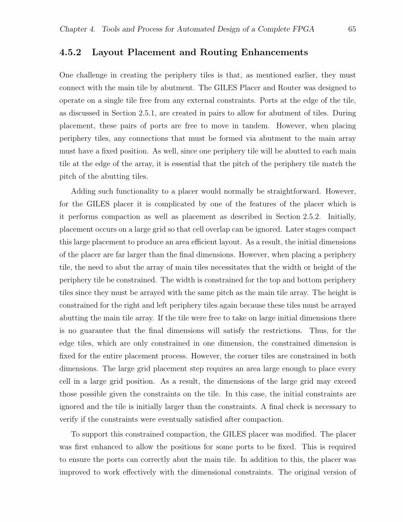
Chapter 4. Tools and Process for Automated Design of a Complete FPGA 65
4.5.2 Layout Placement and Routing Enhancements
One challenge in creating the periphery tiles is that, as mentioned earlier, they must
connect with the main tile by abutment. The GILES Placer and Router was designed to
operate on a single tile free from any external constraints. Ports at the edge of the tile,
as discussed in Section 2.5.1, are created in pairs to allow for abutment of tiles. During
placement, these pairs of ports are free to move in tandem. However, when placing
periphery tiles, any connections that must be formed via abutment to the main array
must have a fixed position. As well, since one periphery tile will be abutted to each main
tile at the edge of the array, it is essential that the pitch of the periphery tile match the
pitch of the abutting tiles.
Adding such functionality to a placer would normally be straightforward. However,
for the GILES placer it is complicated by one of the features of the placer which is
it performs compaction as well as placement as described in Section 2.5.2. Initially,
placement occurs on a large grid so that cell overlap can be ignored. Later stages compact
this large placement to produce an area efficient layout. As a result, the initial dimensions
of the placer are far larger than the final dimensions. However, when placing a periphery
tile, the need to abut the array of main tiles necessitates that the width or height of the
periphery tile be constrained. The width is constrained for the top and bottom periphery
tiles since they must be arrayed with the same pitch as the main tile array. The height is
constrained for the right and left periphery tiles again because these tiles must be arrayed
abutting the main tile array. If the tile were free to take on large initial dimensions there
is no guarantee that the final dimensions will satisfy the restrictions. Thus, for the
edge tiles, which are only constrained in one dimension, the constrained dimension is
fixed for the entire placement process. However, the corner tiles are constrained in both
dimensions. The large grid placement step requires an area large enough to place every
cell in a large grid position. As a result, the dimensions of the large grid may exceed
those possible given the constraints on the tile. In this case, the initial constraints are
ignored and the tile is initially larger than the constraints. A final check is necessary to
verify if the constraints were eventually satisfied after compaction.
To support this constrained compaction, the GILES placer was modified. The placer
was first enhanced to allow the positions for some ports to be fixed. This is required
to ensure the ports can correctly abut the main tile. In addition to this, the placer was
improved to work effectively with the dimensional constraints. The original version of
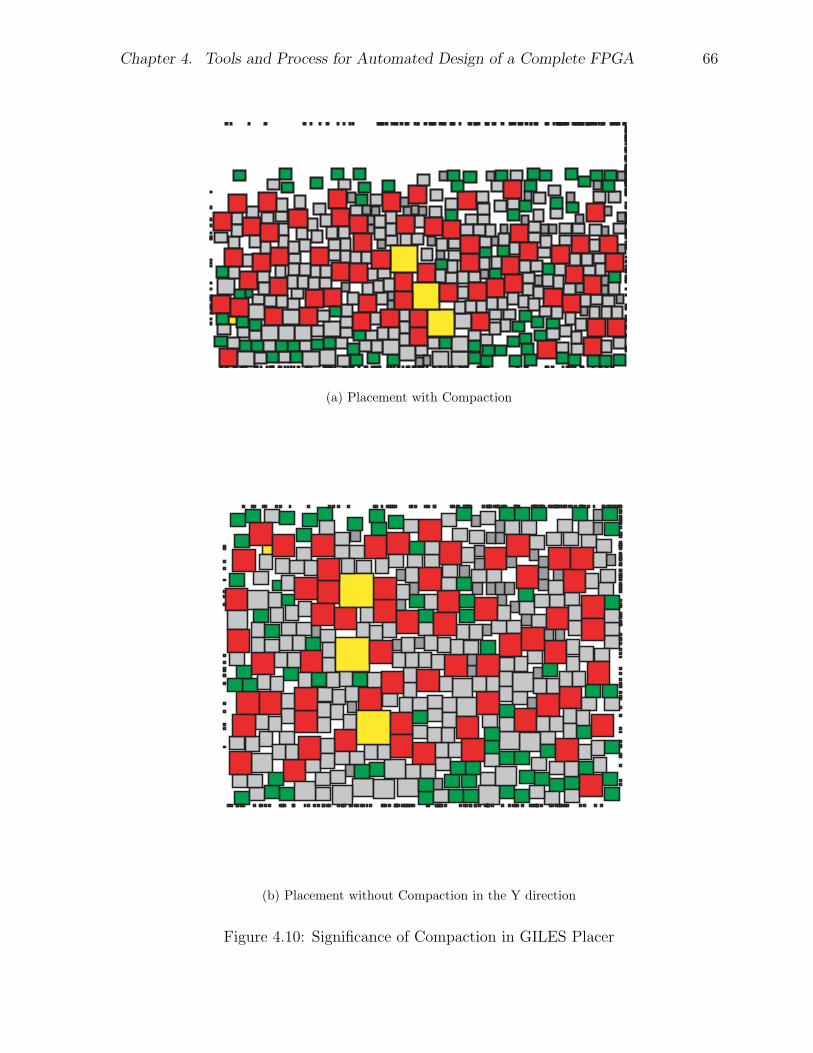
Chapter 4. Tools and Process for Automated Design of a Complete FPGA 66
(a) Placement with Compaction
(b) Placement without Compaction in the Y direction
Figure 4.10: Significance of Compaction in GILES Placer

Chapter 4. Tools and Process for Automated Design of a Complete FPGA 67
the placer attempts to compact the tile in both dimensions but when one dimension is
constrained there is no need for such behaviour. Continued compaction of the constrained
dimension only leads to wasted area as illustrated in an example placement shown in
Figure 4.10(a). It would be more efficient to place cells uniformly within the available
area. Accordingly, the placer was changed to eliminate compaction moves when such
moves are unnecessary. Figure 4.10(b) demonstrates an example of a placement produced
by this updated version of the placer. This modification improves the final area because
it eliminates the unnecessary whitespace within the tile.
4.6 Configuration SRAM Programmer
One of the main advantages of FPGAs is their reconfigurability. Programmable connec-
tions are controlled by configuration SRAM bits. To implement a circuit on the FPGA,
these configuration SRAM bits must be set appropriately. This configuration is known
as a bitstream. At power up and when a new circuit is to be implemented on the FPGA,
this bitstream must be loaded to set all the configuration SRAM in the appropriate state.
This task is performed by a dedicated programmer circuit that communicates with an
external circuit that provides the bitstream information. This section will describe the
design of a generic programmer that accomplishes this task for the automatically laid
out FPGA produced as part of this work.
First, it is necessary to review the basic configuration SRAM architecture assumed
by the GILES layout tools. The SRAM bits are treated as forming a large memory array.
Each bit is connected to a word and bit line which are used to program the bit. These
word and bit lines run the length of the FPGA array in orthogonal directions. This
ensures each bit has a unique position in the memory array just as in normal SRAM
banks. The individual SRAM bits are constructed using five transistors to reduce area
requirements [5]. This also simplifies routing since only a single bit line is required. To
program the SRAM contents, every memory word must be loaded with its configuration
and the programmer circuit is designed to accomplish this task.
4.6.1 Programmer Design
For this test chip, it is desirable to make the programming circuit as simple as possi-
ble to minimize the chance of design error. Programming speed will not be considered
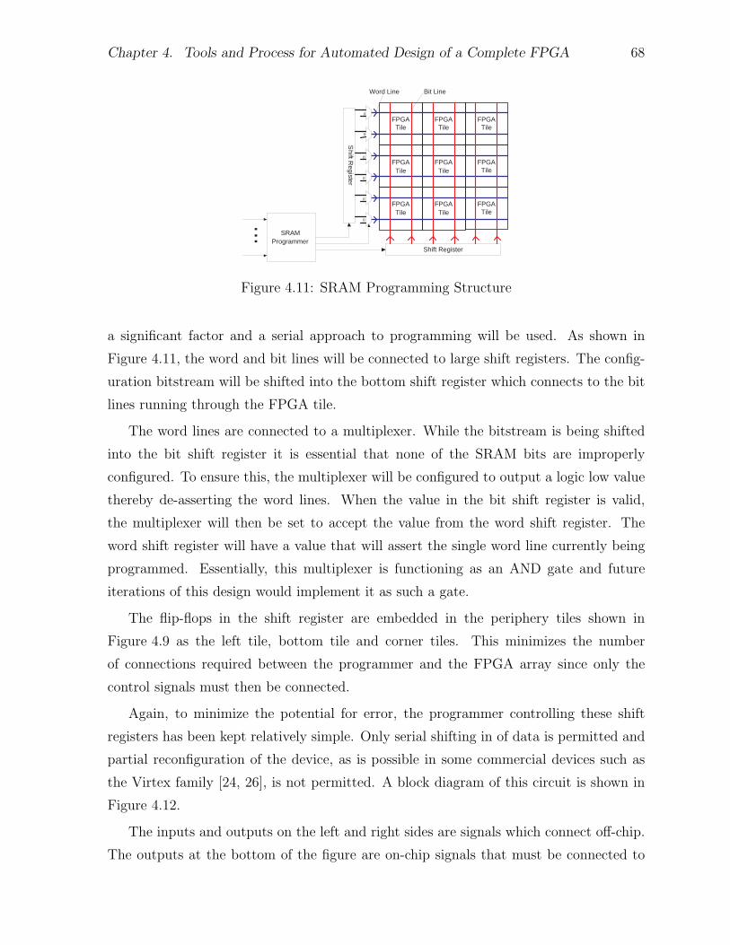
Chapter 4. Tools and Process for Automated Design of a Complete FPGA 68
FPGATile
FPGATile
FPGATile
FPGATile
FPGATile
FPGATile
FPGATile
FPGATile
FPGATile
Shift Register
Shift R
egister
0
0
0
0
0
0
Word Line Bit Line
SRAMProgrammer
...
Figure 4.11: SRAM Programming Structure
a significant factor and a serial approach to programming will be used. As shown in
Figure 4.11, the word and bit lines will be connected to large shift registers. The config-
uration bitstream will be shifted into the bottom shift register which connects to the bit
lines running through the FPGA tile.
The word lines are connected to a multiplexer. While the bitstream is being shifted
into the bit shift register it is essential that none of the SRAM bits are improperly
configured. To ensure this, the multiplexer will be configured to output a logic low value
thereby de-asserting the word lines. When the value in the bit shift register is valid,
the multiplexer will then be set to accept the value from the word shift register. The
word shift register will have a value that will assert the single word line currently being
programmed. Essentially, this multiplexer is functioning as an AND gate and future
iterations of this design would implement it as such a gate.
The flip-flops in the shift register are embedded in the periphery tiles shown in
Figure 4.9 as the left tile, bottom tile and corner tiles. This minimizes the number
of connections required between the programmer and the FPGA array since only the
control signals must then be connected.
Again, to minimize the potential for error, the programmer controlling these shift
registers has been kept relatively simple. Only serial shifting in of data is permitted and
partial reconfiguration of the device, as is possible in some commercial devices such as
the Virtex family [24, 26], is not permitted. A block diagram of this circuit is shown in
Figure 4.12.
The inputs and outputs on the left and right sides are signals which connect off-chip.
The outputs at the bottom of the figure are on-chip signals that must be connected to
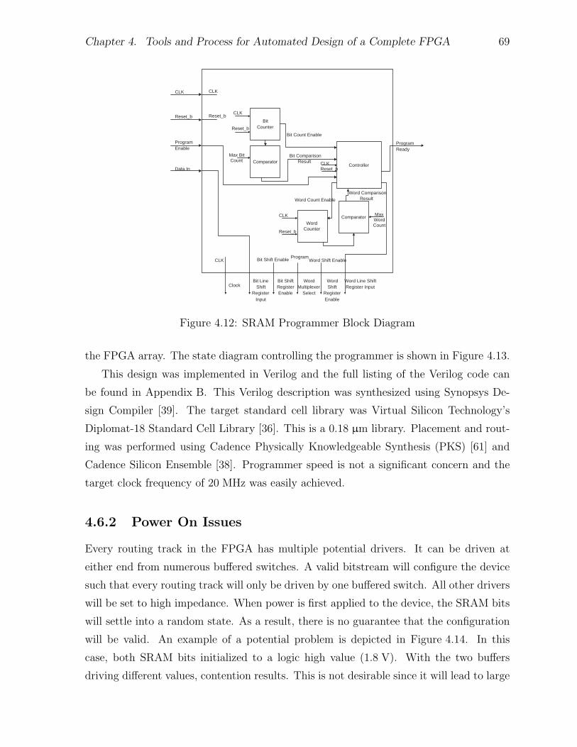
Chapter 4. Tools and Process for Automated Design of a Complete FPGA 69
BitCounter
WordCounter
ComparatorController
CLK
Data In
Reset_b
ProgramReady
ProgramEnable
Reset_b
Reset_b
Reset_b
CLK
CLK
CLK
Max BitCount
Bit Count Enable
Word Count Enable
Bit ComparisonResult
MaxWordCount
Comparator
Word ComparisonResult
Bit LineShift
RegisterInput
Word Line ShiftRegister Input
CLK
Reset_b
Clock
CLK Word Shift Enable
WordShift
RegisterEnable
Program
WordMultiplexer
Select
Bit ShiftRegisterEnable
Bit Shift Enable
Figure 4.12: SRAM Programmer Block Diagram
the FPGA array. The state diagram controlling the programmer is shown in Figure 4.13.
This design was implemented in Verilog and the full listing of the Verilog code can
be found in Appendix B. This Verilog description was synthesized using Synopsys De-
sign Compiler [39]. The target standard cell library was Virtual Silicon Technology’s
Diplomat-18 Standard Cell Library [36]. This is a 0.18 µm library. Placement and rout-
ing was performed using Cadence Physically Knowledgeable Synthesis (PKS) [61] and
Cadence Silicon Ensemble [38]. Programmer speed is not a significant concern and the
target clock frequency of 20 MHz was easily achieved.
4.6.2 Power On Issues
Every routing track in the FPGA has multiple potential drivers. It can be driven at
either end from numerous buffered switches. A valid bitstream will configure the device
such that every routing track will only be driven by one buffered switch. All other drivers
will be set to high impedance. When power is first applied to the device, the SRAM bits
will settle into a random state. As a result, there is no guarantee that the configuration
will be valid. An example of a potential problem is depicted in Figure 4.14. In this
case, both SRAM bits initialized to a logic high value (1.8 V). With the two buffers
driving different values, contention results. This is not desirable since it will lead to large
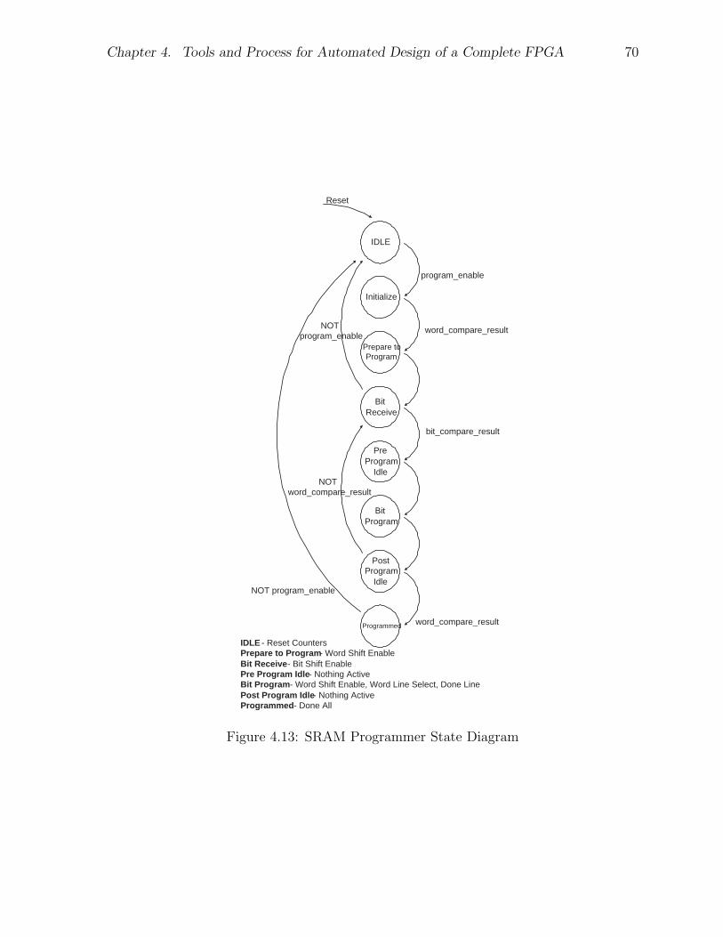
Chapter 4. Tools and Process for Automated Design of a Complete FPGA 70
IDLE
BitReceive
Reset
BitProgram
program_enable
bit_compare_result
word_compare_result
NOTword_compare_result
NOTprogram_enable
IDLE - Reset Counters
Bit Receive - Bit Shift Enable
Bit Program - Word Shift Enable, Word Line Select, Done Line
Programmed
NOT program_enable
Programmed - Done All
Initialize
Prepare toProgram
word_compare_result
PreProgram
Idle
PostProgram
Idle
Prepare to Program - Word Shift Enable
Pre Program Idle - Nothing Active
Post Program Idle - Nothing Active
Figure 4.13: SRAM Programmer State Diagram
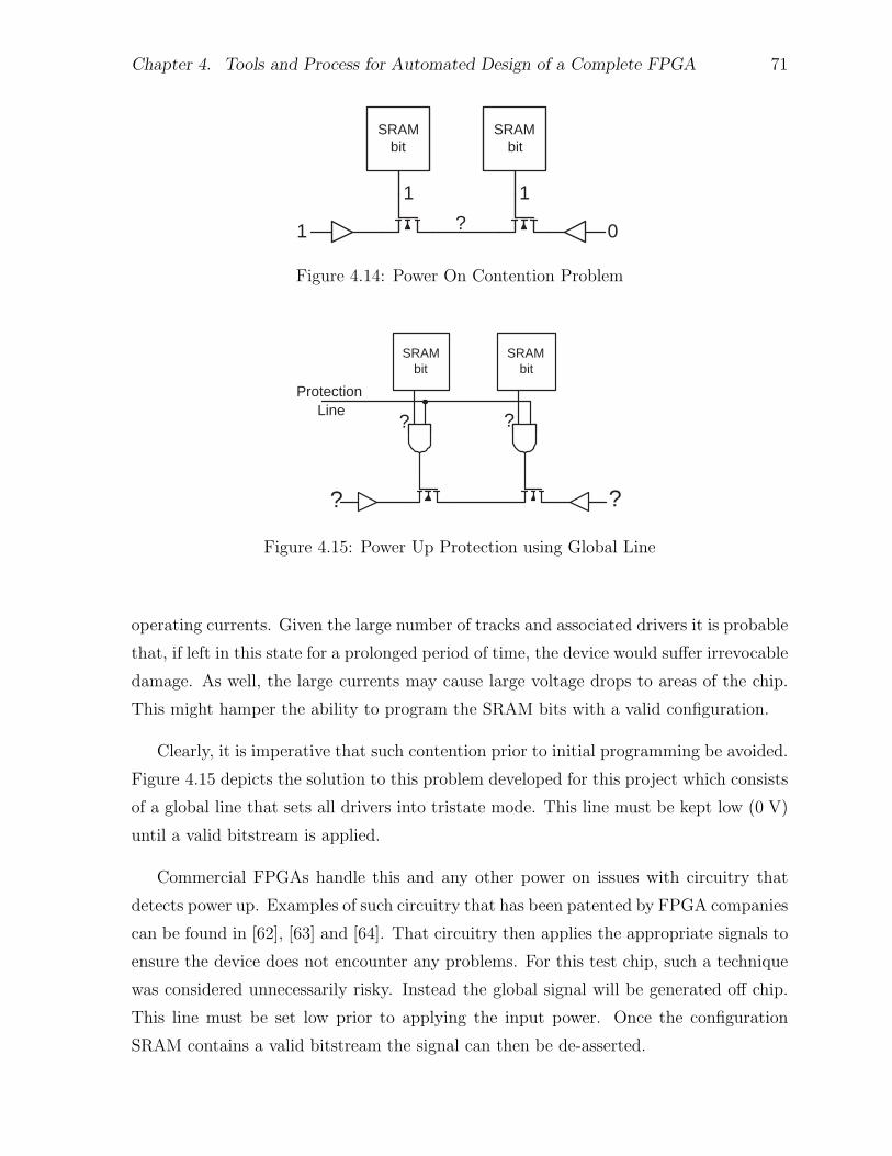
Chapter 4. Tools and Process for Automated Design of a Complete FPGA 71
SRAMbit
SRAMbit
0?1
1 1
Figure 4.14: Power On Contention Problem
SRAMbit
SRAMbit
??
? ?
ProtectionLine
Figure 4.15: Power Up Protection using Global Line
operating currents. Given the large number of tracks and associated drivers it is probable
that, if left in this state for a prolonged period of time, the device would suffer irrevocable
damage. As well, the large currents may cause large voltage drops to areas of the chip.
This might hamper the ability to program the SRAM bits with a valid configuration.
Clearly, it is imperative that such contention prior to initial programming be avoided.
Figure 4.15 depicts the solution to this problem developed for this project which consists
of a global line that sets all drivers into tristate mode. This line must be kept low (0 V)
until a valid bitstream is applied.
Commercial FPGAs handle this and any other power on issues with circuitry that
detects power up. Examples of such circuitry that has been patented by FPGA companies
can be found in [62], [63] and [64]. That circuitry then applies the appropriate signals to
ensure the device does not encounter any problems. For this test chip, such a technique
was considered unnecessarily risky. Instead the global signal will be generated off chip.
This line must be set low prior to applying the input power. Once the configuration
SRAM contains a valid bitstream the signal can then be de-asserted.

Chapter 4. Tools and Process for Automated Design of a Complete FPGA 72
Bit “A” Bit “B”
Track 2Track 4Track 1Track 3
Bit “A” Bit “B”
Track 1Track 2Track 3Track 4
Figure 4.16: Example of Logically Equivalent Changes
4.7 Bitstream Generation
As discussed previously, a bitstream must be created for an FPGA to be used. This
bitstream configures the FPGA for the specific circuit being implemented on the FPGA.
With approximately 20 736 configuration bits in this test FPGA, an automated process
for generating a bitstream is required. As part of this work, such a tool was developed.
First, it is necessary to recall one feature of GILES discussed in Section 2.5.2 which is
the ability to exploit the logical equivalencies present in the FPGA netlist. This allows the
placer to swap output terminals of an SRAM bit, to switch the word and bit lines used for
an SRAM, and to swap multiplexer inputs. An example of this is shown in Figure 4.16.
These features improve placement quality but also alter the netlist electrically from that
which was input to the placer. When generating a bitstream, these changes must of
course be known. As a result, bitstream generation can only be performed after all the
tiles have been placed and routed.
Once the tile design is complete, the process of generating the bitstream can be
started. The inputs to this process are the netlists describing the design and a routing of
the circuit to be implemented on the FPGA. The output is the configuration information
for every SRAM bit in the FPGA.
The bitstream generation process begins by first reading in the tile netlists. Every
programmable element such as a multiplexer or buffered switch is identified along with the
configuration SRAM bits which control it. At this point, the generator also determines
which SRAM output, data or inverse data, is used as the control signal.
The routing of the circuit that will be implemented on the FPGA is produced by
the VPR Placer and Router. It is described in terms of paths within an internal graph
structure that abstractly describes the routing network of the FPGA. This graph, known
as the routing resource graph, hides the actual implementation of the FPGA from the
VPR Placer and Router. Physically, though, each edge in this graph corresponds to
Chapter 4. Tools and Process for Automated Design of a Complete FPGA 73
programmable element while each node corresponds to a wire or net. Prior to generating
a bitstream, the bitstream generator must determine the association between the routing
resource graph edges used by the router and the programmable elements in the circuit.
With just a regular netlist, matching the elements is challenging since many similar
elements exist. To avoid these difficulties, information was added to the netlist to assist
in the identification process. In particular, the resource type, resource number, switch
type, and original coordinates are saved with the netlist. Using this information, every
programmable element is appropriately labelled by the bitstream generator.
Once all the programmable elements have been identified, the bitstream generator
must next determine the safe state for all the SRAM in the device. This will be the
default state for each of the SRAM bits. This safe state will ensure that no contention
occurs on routing tracks. While the programmable elements inside the logic cluster do
not present the opportunity for contention, it is also necessary to configure them ap-
propriately by default. If randomly configured it is possible to create ring oscillators
inadvertently. This can occur anytime there is a combinational loop with a LUT config-
ured as an inverting element. The loop can be created by the default configuration of the
intra-cluster routing since the cluster outputs are available as inputs to the LUT input
multiplexers. Such a situation should be avoided for multiple reasons. In simulation, an
unnecessary ring oscillator would slow down simulation. In silicon, the oscillator would
increase power consumption and potentially add noise to other signals on the FPGA. It
should be emphasized that unlike commercial devices such as Altera’s Cyclone [65], there
is not a bias toward SRAM configured in the zero state. Due to the logically equivalent
changes by the GILES placer, producing the safe configuration state for the logic cluster
is not simply a matter of setting the SRAM bits to zero. Instead, the proper configuration
must be determined based on the tile netlist.
The routing produced by the VPR Router can now be implemented. The bitstream
generator processes each routing resource graph path required by the VPR Router. For
each path, the generator identifies each programmable element needed for the connec-
tions and programs the element accordingly. This graph does not describe any of the
connections within the logic cluster nor does the VPR placer specify placement of the
individual BLEs. The placer only operates on the cluster level. Instead, the placement
of the BLEs is dictated by the final routing. Based on which cluster output is selected by
the VPR router, the bitstream generator then selects the placement of the BLE within
the cluster. Once this placement is set the LUT inputs and the LUT mask are appropri-
Chapter 4. Tools and Process for Automated Design of a Complete FPGA 74
ately configured. In cases where there are unused LUT inputs, the mask for configuring
the LUT is updated to treat the signals as don’t cares. The complete bitstream is then
output in various formats suitable for simulation and silicon.
It should also be noted that the bitstream generator is not specific to the FPGA con-
structed for this work. The tool is capable of handling the range of tileable architectures
that can be produced by the GILES automated layout tools.
4.8 Summary
With the tools presented, it is now possible to automatically design and use an FPGA
created with the GILES tools. The process of doing so will now be outlined to highlight
the contributions of this work. Starting from an architecture description, prior work
enabled the automatic design of the main FPGA tile. This work has extended the
GILES layout tools significantly. From the main FPGA tile, seven additional periphery
tiles can be automatically created. These tiles are needed to complete an FPGA array
and the GILES tools have been updated to accommodate the constraints associated with
periphery tiles. Given a complete FPGA, VPR was modified to enable it to perform
placement and routing on this generated FPGA. With the bitstream generator created
in this work, this placement and routing can be mapped to the physical implementation
of the FPGA and a bitstream to configure either a simulated version or the real version
of the device can be produced. A programmer circuit was designed that enables this
bitstream to be used to program the configuration SRAM distributed throughout the
FPGA tiles. It is significant to note that none of this work is architecture specific and
any VPR LAYOUT/GILES architecture can be targeted.
When this work is combined with concurrent work performed by Egier in [22] that
created the physical layouts of the cells used by GILES, updated GILES to use a com-
mercial router and addressed global layout challenges such as power, ground and clock
distribution, producing a complete FPGA with the architecture described in Section 4.4
is now possible. The final layout that was created is shown in Figure 4.17. The challenge
that remains is to verify that a functional FPGA is being produced. The verification
methodology and the results from simulation that demonstrate the design is functional
will be presented in the following chapter.

Chapter 4. Tools and Process for Automated Design of a Complete FPGA 75
Figure 4.17: Complete FPGA Layout

Chapter 5
Verification Methodology and
Results
5.1 Introduction
The system presented in Chapter 4 enables the automated design of an entire FPGA.
However, thorough testing has never been performed on the entire automated flow, from
circuit generation to layout, to verify that the design is implemented correctly. Prior
to fabrication, this shortcoming must be addressed and extensive verification must be
performed to ensure that the design sent for manufacturing will operate correctly when
silicon is returned. There are many different issues that must be considered in verification
and, thus, the goals for this device must first be examined.
For this design, proper functionality is paramount. The speed at which the circuit
can operate is not as high a priority to keep the scope of this work tractable. Therefore,
the current verification effort will focus exclusively on ensuring a functional FPGA is
designed and produced. There are three basic issues that must be considered.
First, does the circuit implement the desired FPGA architecture? The automatic
layout tools have only been subject to approximate manual inspection in the past. It is
not certain that the netlist produced by GILES Netlist Generator or the changes made by
the GILES Placer are correct and meet expectations. The VPR Architecture Generator
has been updated to match the expected results from the automatic layout and this must
be compared with the actual netlist produced by the GILES layout tools to prove that
the two structures are identical.
Another issue is whether a circuit can be implemented on this FPGA fabric. VPR has
76
Chapter 5. Verification Methodology and Results 77
only been used for architectural explorations previously so it is not certain that circuits
implemented on the FPGA are correctly placed and routed by VPR. More significantly,
the bitstream generator which translates a routing produced by the VPR Placer and
Router to an implementation on the FPGA fabric has not been used previously and its
correctness must be verified.
Finally, since an automatically laid out design generated by the GILES tools is being
fabricated, a plethora of issues regarding the correct electrical functionality of the circuit
arise. Each cell is a custom design that has never been used previously and as a result is
uncharacterized. Ensuring that all the cells used by the GILES tools operate successfully
is a significant challenge.
This chapter will present the verification efforts used to address these concerns. First,
the overall strategy will be presented. Then each aspect of verification will be considered
along with the results of such testing.
5.2 General Verification Strategy
Verifying a design of the size of this FPGA is a challenge since in each tile there are 530
cells and in total the design has over 300 000 transistors. Therefore, the circuit is too
large for each element to be individually tested and, instead, alternate techniques must
be used. A few classes of approaches will be used ranging from simple circuit comparisons
to simulation-based methods.
The most basic approach will be an automated comparison of the architecture pro-
duced by the VPR Architecture Generator and that which is produced by the automatic
layout tools. The architecture from the Architecture Generator will be in the form of
a routing resource graph describing all the connections in available in VPR. The auto-
mated check will ensure that each of the edges in these graphs matches a resource in the
netlist. This will confirm that the functionality assumed by the CAD tools supporting
the design is present. The success of this test is necessary since the CAD tools such as the
bitstream generator depend on the VPR architecture and the physical implementation
being identical. Without these tools, further testing is not possible; however, this basic
comparison does not confirm the proper operation of the design.
To better verify that the design and the CAD tools are functional, simulation will
be used. These simulations will be performed for several levels of abstraction to trade-
off simulation speed for accuracy. At the highest level of abstraction and fast speed of

Chapter 5. Verification Methodology and Results 78
simulation, only the logical functionality will be considered. This will treat all signals
as being digital and issues such as drive strength and timing will be neglected. Such
simulations will test the ability to configure the FPGA properly as well as ensuring the
connectivity inside the FPGA array is as expected.
At a level lower from this, the true analog nature of the circuit will be considered.
Instead of Register Transfer Level (RTL) gate descriptions, cells will be implemented
using transistors. This allows electrical issues to be observed. Simulating each cell to
confirm its proper analog behaviour, while useful and necessary, is not sufficient since
more complicated interactions occur when the electrical behaviour is considered. In
particular, given the liberal use of pass transistors throughout this design as part of
multiplexers and tri-state drivers, voltages will not simply be high (VDD) or low (VSS)
and instead a range of possibilities will definitely occur. Therefore, these electrical checks
are important as they are needed to confirm that each cell can function within the larger
circuit.
The next levels of simulation will increase the use of information extracted from actual
circuit layouts. Instead of relying on a structural netlist produced by the automated
layout tools and cell-level netlists extracted from layouts, larger portions of the design
will be extracted from the layouts. Both an extracted netlist from the individual tiles and
the entire chip will be used for simulation. In this final stage, there will be no reliance
on netlists from the automated tools. This is necessary to confirm that all the cells and
tiles function together properly and, hence, the actual layout is acceptable.
Finally, as an additional check between what is used in simulation and the layout
produced automatically, Layout versus Schematic (LVS) comparisons will be performed.
This will confirm that the thoroughly simulated designs are in fact implemented in the
layout. This serves as alternate check, in parallel, to the simulation of the extracted chip.
5.3 Routing Resource Graph to Netlist Matching
As described in Chapter 4, the routing structure and BLE structure assumed by the
VPR Architecture Generator has been updated to reflect the structure that is produced
using the automatically generated tiles. However, it has not been confirmed that the two
structures are in fact the same. Thus, an appropriate first verification step is to compare
the VPR architecture structure with that which is produced by the GILES automated
FPGA creation and layout tools.
Chapter 5. Verification Methodology and Results 79
The procedure for performing this comparison is as follows. The tile cell-level netlists
are read in by the bitstream generator. As discussed in Section 4.7, the tool then attempts
to match the programmable elements in the netlists with the logical resources used by
the VPR Placer and Router. In general, the bitstream generator need only consider the
logical resources explicitly required for the circuit being implemented. However, as a
check, the bitstream generator was configured to search for every possible logical element
available to the VPR Placer and Router. This ensures that any placement and routing
produced by VPR is suitable for bitstream generation. Such a check is important since
it will confirm that the tiles generated with the GILES tools contain all the circuitry
required to implement the logical structure assumed by VPR. Later stages of verification
will confirm that the GILES-generated tiles match the physical layouts.
It is significant to note that this most basic test found a wide range of problems with
initial versions of the tiles. The version of the netlist generator developed by Padalia in [5]
did not include some of the programmable connections used by VPR. These deficiencies
were identified and corrected. The version used for fabrication successfully passes this
verification step.
5.4 Logical Functionality
As discussed previously, verification of the logical functionality will be the first test that
demonstrates the design and its supporting tools are functional. The test environment,
test circuits and results will be described in the following sections.
5.4.1 Methodology
The inputs to this stage of the verification process are the netlists that describe the
FPGA tiles and a test circuit that will be implemented on the FPGA. The output will be
the simulation results using these tiles. A custom tool was developed as part of this work
to assist in this process. This tool will be referred to as the VPR LAYOUT Simulation
Generator. It accepts the tile netlists as inputs and then outputs a description of a
complete arrayed FPGA in a format suitable for simulation.
The input tile netlists are produced by the GILES automated FPGA layout tools. The
Simulation Generator reads these netlists. It then outputs a hierarchical description of
the complete FPGA. The basic cells used by the layout tools constitute the lowest level of

Chapter 5. Verification Methodology and Results 80
the hierarchy. A library of RTL descriptions of the cells will define their behaviour during
simulation. At a step higher in the hierarchy, these cells are then connected together to
form the tiles described by the input tile netlists. As discussed in Section 4.5, there are
eight different tiles and at the next level of hierarchy these tiles are connected together
to form the FPGA array structure shown in Figure 4.9. At this level, the programmer
designed in Section 4.6 is also instantiated. Pad cells taken from the Virtual Silicon
Technology 0.18 µm Diplomat standard cell library [36] are also connected to the input
and output signals in the array of tiles. The clock and the power-on protection signal
are assumed to be globally connected to every tile. The entire hierarchical description of
the FPGA is output in Verilog.
The test circuit will be input as a BLIF file. Following the bitstream generation pro-
cedure discussed in Section 4.7, the VPR Bitstream Generator will produce a bitstream
that configures the FPGA to implement the test circuit. To verify that the tools and
the automatically generated FPGA are operating correctly, the behaviour of the FPGA
must be compared to the results expected for the test circuit. The BLIF input file de-
fines the expected behaviour. To perform the comparison the BLIF circuit description is
converted to Verilog using an automated tool created for the current work.
Simulation is performed using Cadence NC-Verilog [66]. No timing information is
used and all gates operate with zero delay. The bitstream produced by the bitstream
generator is applied to the programmer which then programs the configuration bits in the
FPGA array. Once programming is complete, test vectors are applied to the FPGA array
inputs and the outputs from the FPGA array are compared to the outputs from Verilog
implementation of the original BLIF test circuit description. The two implementations
should match exactly except in the case of uninitialized sequential circuits. The flip
flops in the FPGA array do not have a dedicated reset signal. It is possible to construct
a synchronous reset using LUTs but for circuits already described in BLIF form such
functionality is not easily added. As a result, care must be taken in the comparisons
between the FPGA array and the BLIF description when flip flops are present. Either
sequential circuits are avoided or comparison will only be performed after all the flip flops
have been initialized to a known state.
Chapter 5. Verification Methodology and Results 81
5.4.2 Test Circuits
To verify the functionality of the FPGA, test circuits must be developed or obtained.
These circuits will be implemented on the test FPGA. Due to the VPR-based CAD flow,
these circuits must be available as BLIF netlists.
Given that there are 20 736 configuration SRAM in the FPGA array, a very large
number of possible configurations exist. It is not possible nor is it prudent to test every
possible valid configuration. The goal in this verification effort is simply to establish that
a range of designs can be successfully implemented on the FPGA. This will demonstrate
that the GILES netlist generator and the bitstream generator function adequately. Other
tests such as those performed in Section 5.3 increase the confidence that the output from
the netlist generator is correct. Hence, only a relatively small number of test circuits are
needed.
For some specific needs, custom test circuits were developed. These tests target basic
functionality of the FPGA and were used to assist in debugging early versions of the
GILES CAD flow. In addition to these custom tests, other circuits were obtained as well.
The MCNC circuits [60] were released for benchmarking CAD tools but they are also
useful simply as black box test circuits. The function they implement is not important
and it is only imperative that the implementation of the circuit on the FPGA match the
expected output based on the input BLIF file. The primary circuits that are used for
testing are listed in Table 5.1. The size of the circuit in terms of logic clusters, inputs and
outputs is given along with the source of the circuit. At various times in the verification
effort, other test circuits have been used; however, Table 5.1 only catalogues the tests
which were considered most important. Altering the placement results in a different
routing and hence a different bitstream. For some of the circuits, various placements
were attempted but, for the tests listed in the table, only the default placement obtained
by using VPR with the default placement seed will be used for the basic suite of tests.
The majority of the circuits listed in Table 5.1 are purely combinational. Due to the
aforementioned difficulties in reseting the sequential circuits, combinational circuits are
more useful for testing. From a functionality perspective, the only difference between a
sequential circuit and a combinational design is the select lines in the output multiplexer
of the BLEs. Hence, it is sufficient to only test the flip flops using the shift register circuit.
This circuit will confirm that the flip flops can be used and the remaining circuits will
more thoroughly test the LUTs and routing.
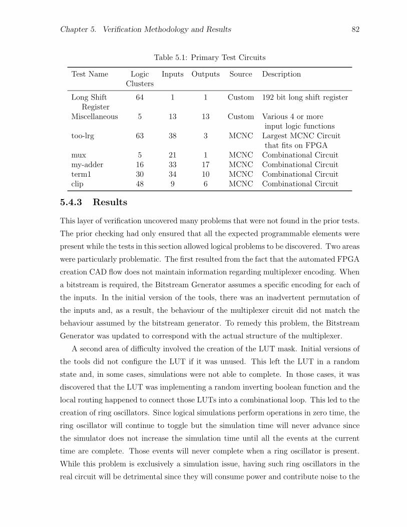
Chapter 5. Verification Methodology and Results 82
Table 5.1: Primary Test Circuits
Test Name Logic Inputs Outputs Source DescriptionClusters
Long Shift 64 1 1 Custom 192 bit long shift registerRegister
Miscellaneous 5 13 13 Custom Various 4 or moreinput logic functions
too-lrg 63 38 3 MCNC Largest MCNC Circuitthat fits on FPGA
mux 5 21 1 MCNC Combinational Circuitmy-adder 16 33 17 MCNC Combinational Circuitterm1 30 34 10 MCNC Combinational Circuitclip 48 9 6 MCNC Combinational Circuit
5.4.3 Results
This layer of verification uncovered many problems that were not found in the prior tests.
The prior checking had only ensured that all the expected programmable elements were
present while the tests in this section allowed logical problems to be discovered. Two areas
were particularly problematic. The first resulted from the fact that the automated FPGA
creation CAD flow does not maintain information regarding multiplexer encoding. When
a bitstream is required, the Bitstream Generator assumes a specific encoding for each of
the inputs. In the initial version of the tools, there was an inadvertent permutation of
the inputs and, as a result, the behaviour of the multiplexer circuit did not match the
behaviour assumed by the bitstream generator. To remedy this problem, the Bitstream
Generator was updated to correspond with the actual structure of the multiplexer.
A second area of difficulty involved the creation of the LUT mask. Initial versions of
the tools did not configure the LUT if it was unused. This left the LUT in a random
state and, in some cases, simulations were not able to complete. In those cases, it was
discovered that the LUT was implementing a random inverting boolean function and the
local routing happened to connect those LUTs into a combinational loop. This led to the
creation of ring oscillators. Since logical simulations perform operations in zero time, the
ring oscillator will continue to toggle but the simulation time will never advance since
the simulator does not increase the simulation time until all the events at the current
time are complete. Those events will never complete when a ring oscillator is present.
While this problem is exclusively a simulation issue, having such ring oscillators in the
real circuit will be detrimental since they will consume power and contribute noise to the

Chapter 5. Verification Methodology and Results 83
circuit unnecessarily. To address these concerns, the Bitstream Generator was updated
to always initialize unused LUTs to produce a constant logical zero output. This need
for initialization was also discussed in Section 4.7.
Once those problems were remedied, all comparisons between implementation on
the test FPGA and expectations based on the BLIF input file were successful. This
demonstrates a few significant accomplishments. Most importantly, it establishes that
the bitstream generator can function correctly. Also, this reveals that the FPGA array
implements the programmable fabric assumed by VPR.
5.5 Electrical Functionality
Logical functionality testing confirmed that the high-level design of the FPGA is ade-
quate. The circuit-level implementation of this design must also be checked to ensure
that the FPGA will function correctly at the electrical level. To perform these tests, cells
that were previously described logically must now use transistor-based implementations.
This section will describe the testing conducted at this level.
5.5.1 Methodology
The Simulation Generator is used, as in Section 5.4.1, to produce a structural Verilog
netlist describing the FPGA array and the programmer. However, the cells in both
components are replaced with transistor-level implementations. These transistor-level
implementations are extracted from the actual layout of the cell. The parasitic capaci-
tance introduced from the transistors and their interconnect is also extracted from the
actual layout.
A standard tool for performing transistor-level simulations is HSPICE. However, there
are over 300 000 transistors in the complete FPGA design and this exceeds the capacity
of HSPICE. Instead, Synopsys Nanosim [67] is used to simulate the design. Nanosim is
a high-speed, high-capacity circuit simulator reported to have an accuracy within 2% to
5% of HSPICE [68] and it is capable of handling a design of this size. This tool does
allow simulation speed to be increased at the expense of accuracy. The level of accuracy
used in this work was selected based on the recommendations in the tool’s documentation
[67].
Again, a comparison point is needed to ensure the design is functional. Mixed-signal

Chapter 5. Verification Methodology and Results 84
simulation through integration with the Verilog simulator was unsuccessful because of
problems encountered with the tools that could not be fixed in a reasonable amount of
time. Instead every test was first performed using the procedure of Section 5.4.1. The
input and output signals to the array and programmer are captured and then converted
to vectors. These input vectors are applied in the Nanosim simulation to the design and
the output vectors confirm the proper functionality. The test circuits listed in Table 5.1
were also used for these electrical functionality tests.
5.5.2 Results
The importance of this verification step can be seen in the number of problems uncovered
by this testing. It had been thought that HSPICE simulation of typical paths within the
FPGA would reveal most potential problems. However, Nanosim simulation uncovered
a host of problems particularly involving the use of a PMOS pull-up to restore voltages
degraded after passing through NMOS pass transistors. Sizing of this pull-up is a delicate
task since, if it is too strong, it will not be possible to pull down nodes connected to the
pull-up and, if it is too weak, area will be wasted since the length must be increased
to make the device weaker than a minimum width transistor. Due to the on-resistance
of NMOS pass transistors, problems were discovered in paths involving many series-
connected pass transistors. Initial size adjustments remedied these problems for typical
transistor models but more thorough testing using the corner models revealed additional
problems requiring correction. These paths were not considered in the initial SPICE
simulations and only thorough application of this electrical functionality verification led
to the discovery of these potentially fatal problems.
All tests successfully passed with the primary test circuits. These circuits were tested
with typical NMOS and PMOS transistor models and the standard core voltage for this
process of 1.8 V. As an additional check, some test circuits were simulated using corner
models (Slow P Slow N, Fast P Fast N, Slow P Fast N, Fast N Slow P) for the transistors.
As well, the circuit was tested with VDD at 1.62 V which is 10% below nominal. The
FPGA design was found to be operate successfully under all these conditions.
5.5.3 Test Coverage
The goal of this verification effort was to confirm functionality of the entire design. It
is thus relevant to measure the amount of the design that has been tested. A variety of
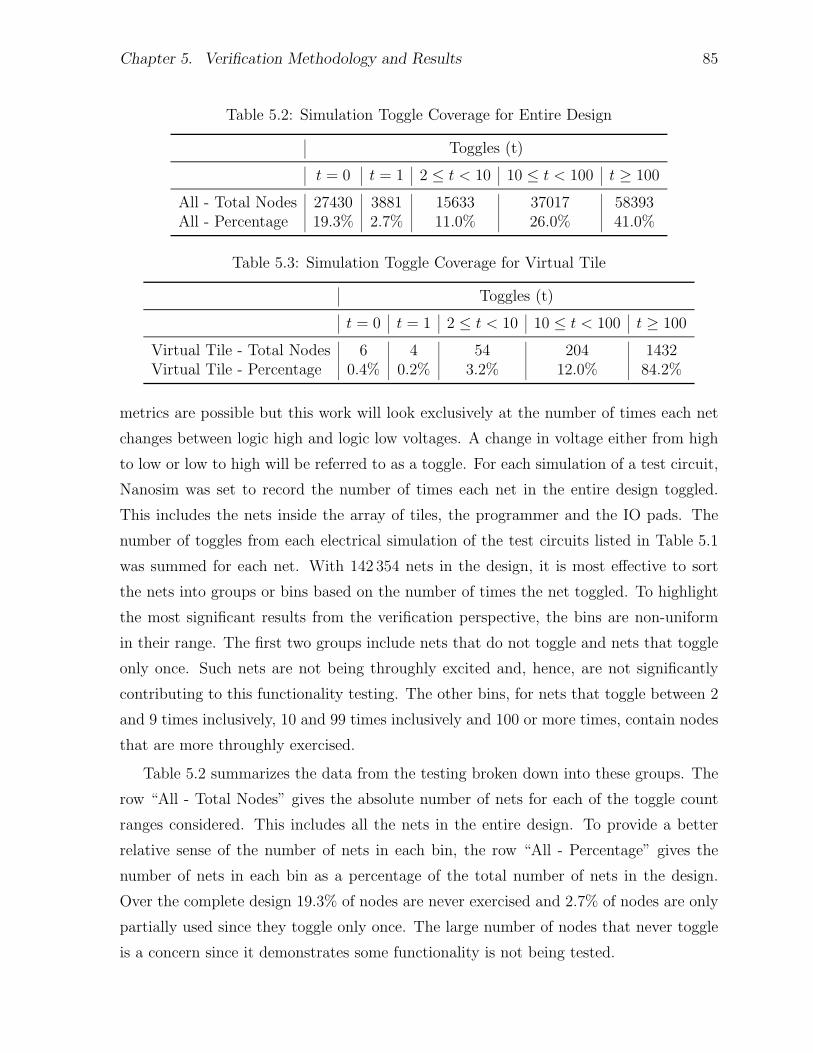
Chapter 5. Verification Methodology and Results 85
Table 5.2: Simulation Toggle Coverage for Entire Design
Toggles (t)
t = 0 t = 1 2 ≤ t < 10 10 ≤ t < 100 t ≥ 100
All - Total Nodes 27430 3881 15633 37017 58393All - Percentage 19.3% 2.7% 11.0% 26.0% 41.0%
Table 5.3: Simulation Toggle Coverage for Virtual Tile
Toggles (t)
t = 0 t = 1 2 ≤ t < 10 10 ≤ t < 100 t ≥ 100
Virtual Tile - Total Nodes 6 4 54 204 1432Virtual Tile - Percentage 0.4% 0.2% 3.2% 12.0% 84.2%
metrics are possible but this work will look exclusively at the number of times each net
changes between logic high and logic low voltages. A change in voltage either from high
to low or low to high will be referred to as a toggle. For each simulation of a test circuit,
Nanosim was set to record the number of times each net in the entire design toggled.
This includes the nets inside the array of tiles, the programmer and the IO pads. The
number of toggles from each electrical simulation of the test circuits listed in Table 5.1
was summed for each net. With 142 354 nets in the design, it is most effective to sort
the nets into groups or bins based on the number of times the net toggled. To highlight
the most significant results from the verification perspective, the bins are non-uniform
in their range. The first two groups include nets that do not toggle and nets that toggle
only once. Such nets are not being throughly excited and, hence, are not significantly
contributing to this functionality testing. The other bins, for nets that toggle between 2
and 9 times inclusively, 10 and 99 times inclusively and 100 or more times, contain nodes
that are more throughly exercised.
Table 5.2 summarizes the data from the testing broken down into these groups. The
row “All - Total Nodes” gives the absolute number of nets for each of the toggle count
ranges considered. This includes all the nets in the entire design. To provide a better
relative sense of the number of nets in each bin, the row “All - Percentage” gives the
number of nets in each bin as a percentage of the total number of nets in the design.
Over the complete design 19.3% of nodes are never exercised and 2.7% of nodes are only
partially used since they toggle only once. The large number of nodes that never toggle
is a concern since it demonstrates some functionality is not being tested.
Chapter 5. Verification Methodology and Results 86
However, as can be seen in the floor plan of the chip in Figure 4.9, the design has a
great deal of regularity since a large portion of the design consists of the array of 8 × 8
main tiles. These main tiles are identical. Instead of considering the entire array of these
tiles as one large structure, the regularity can be used and a single tile will be analyzed.
For each net inside the main tile, the number of times the net toggles in each instantiation
of the main tile will be totalled. The toggle coverage will then be considered in terms of
this virtual tile. The term virtual is used because no actual tile exhibits such toggling.
Yet, given the entire design, the main tile is being exercised in such a manner. Again, the
number of toggles is also summed over all the simulations performed. These results are
shown in Table 5.3. The “Virtual Tile - Total Nodes” gives the number of total number
of nets in each toggle count range for this single virtual tile. This is converted into the
percentage of the nodes in the tile in the row labelled “Virtual Tile - Percentage”. By this
measurement technique only 0.4% of the nodes in this single virtual tile are unexercised
and 0.2% only toggle once. The majority of the nodes, 84.2%, toggle over a hundred
times and this indicates that over the entire design the main tile is being thoroughly
exercised.
Observing this single virtual tile is very different than what is done for manufacturing
tests. It is acceptable since the focus in this testing is functionality. When performing
manufacturing tests, the goal is often to exercise every physical node since manufacturing
defects can occur in any area of the design. However, for simply testing functionality,
the repetition in the design can be used since all the main tiles are identical at design
time. It is only in manufacturing that differences or defects can arise in individual tiles.
One issue with these toggle count observations is that the observability of any faults
is not guaranteed. Ideally, one should ensure that the reported toggles are observed on
the output signals tested by the simulator. This however was not done for this work
and the possibility exists that a significant portion of the functionality is not actually
being observed. For future designs, improved analysis of test coverage would clearly be
desirable.
Despite these observability concerns, the tests performed do increase the confidence in
the design since the test circuits were in fact functional. At the very least, these circuits
should operate on the FPGA and it is quite likely that significantly more circuits will be
functional.
Chapter 5. Verification Methodology and Results 87
5.6 Further Electrical Functionality Checking
To further ensure the correct operation of the FPGA more extensive simulation is needed.
Up to this point a netlist produced by the GILES placer has been used to generate the
Verilog simulation environment. Separate work by Egier in [22] has taken this netlist
from the placer and routed it to produce a final tile layout. These tiles are automatically
arrayed and connected to complete the design. These are significant steps and, thus, it
is essential that their output is verified.
The procedure for these simulations is similar to that used in Section 5.5.1. However,
now more of the physical design is extracted from the actual layouts. Using the Ca-
dence Diva Extractor [69], the layout of an entire tile was first converted to a transistor
level netlist. These transistor-level netlists are then substituted for the Verilog struc-
tural netlist of that same tile that was generated using the VPR LAYOUT Simulation
Generator discussed in Section 5.5.1. With this new transistor-level netlist describing
the design, simulation with Nanosim was performed in the same manner as before. Fi-
nally, this process was repeated except with the layout of the entire FPGA extracted to
a transistor-level netlist.
This level of simulation is computationally intensive. Running on a 1.062 GHz Ultra-
SPARC IIIi processor, the full simulation requires approximately 65 hours. As a result,
time constraints prior to the tape out of this design prevented all the test circuits listed
in Table 5.1 from being used for this verification step. Only the long shift register, mis-
cellaneous, my-adder, and too-lrg test circuits were simulated at this level. Nevertheless,
this does provide reasonable confidence that the design is functional.
5.7 Summary
This multi-faceted approach to verification has demonstrated the functionality of the
design. Initial tests indicated that the structure of the FPGA assumed by VPR matches
that produced using the automated layout tools. Extensive simulation then confirmed
proper operation of this structure and the supporting infrastructure needed to configure
and to use the design. Finally, LVS comparisons between this simulation version and the
physical layout reveals the validity of these simulations.

Chapter 6
Conclusions and Future Work
6.1 Summary
The goal of this thesis was to explore the utility of an automated FPGA design method-
ology by considering two issues: the layout quality and the viability of this method.
First, the area quality of FPGA layouts produced with automated tools was assessed in
Chapter 3. The quality was measured by comparison with manually generated layouts.
This comparison, which was significantly more accurate than past comparisons, found
that the automated tools can produce a layout that is only 36% larger than one created
manually. This is a promising result and it suggests that there is room for automation in
FPGA design. Furthermore, with concentrated effort to improve the tools in the future,
it will likely be possible to automatically create layouts that are more area-efficient than
manual designs.
In Chapters 4 and 5, this work focused on developing the infrastructure needed to
create a complete FPGA. This included the development of tools and circuits, such as a
bitstream generator and a configuration SRAM programmer, that are needed to use an
FPGA. Using those tools, in conjunction with prior automated design tools, a complete
FPGA was created. This design was demonstrated to be functional in simulation and it
was sent for fabrication. Producing and fabricating this complete FPGA is a significant
accomplishment since it demonstrates the feasibility of an automated FPGA design flow.
6.2 Contributions
This thesis made the following contributions:
88
Chapter 6. Conclusions and Future Work 89
• An accurate capture of the Virtex-E for use in layout comparisons.
• A fair comparison between manual and automated layouts which found that layouts
which are only 36% larger can be produced automatically.
• The development of tools that enable the automated creation of a configuration
SRAM programmer and the periphery tiles needed to connect I/O pads to the
main FPGA array.
• The creation of an environment for verifying FPGAs produced using the automated
layout tools. This included the development of a generic bitstream generator and
tools that enable the simulation of an FPGA.
• The creation of a fully functioning chip.
• A complete FPGA design described at the cell level, the electrical level and the
physical layout level that may be of use to academic FPGA architects and creators.
6.3 Future Work
The layout quality and feasibility issues considered in this work suggest many possible
future directions. This work measured the quality of the layouts produced using the
automated tools exclusively in terms of area. Other important parameters like speed
and power consumption should be measured in the future. Once the speed and power
consumption are accurately measured, it would be logical to design tools that can opti-
mize these parameters while still ensuring reasonable area efficiency. The goal would be
to create tools that produce layouts which are faster and more power and area efficient
than the layouts produced by manual designers.
It would also be useful to perform more comparisons to manual layouts in the future.
The single comparison performed in this work was a valid starting point but to better
demonstrate the capabilities of the automated layout tools, comparison to many devices
from various manufacturers using various CMOS processes is needed. If the area, speed
and power performance of the layouts produced automatically is found to be similar to
that of manual layouts then it would provide a strong basis for FPGA manufacturers to
use automated tools for future layouts.

Chapter 6. Conclusions and Future Work 90
One input to the current tools is the set of cells needed by the design. As a result, the
cells have to be created before significant information about the final layout is known.
It would be interesting to reverse this process and create tools that output specifications
for the cells. An initial estimate of the cell’s size and the location of the cell’s input and
output pins could be used as starting point and then both the size and pin positions could
be optimized by the placer and router to suit the layout needs. The required cells would
then be created manually. This process could lead to significantly more area efficient
designs with the only cost being a slight increase in the complexity of the manual layout.
However, that manual effort would remain well below the effort required to create the
complete FPGA layout which could make this a promising technique
Finally, it would also be interesting to augment the current verification tools to fa-
cilitate the measurement of the speed of the FPGA circuit. This information would be
useful for timing-driven placement and routing of circuits on the FPGA since, currently,
for every new target architecture, the user must provide an estimate to the placer and
router of the delays through the FPGA resources. If the performance estimate for a
circuit implemented on an FPGA is to be accurate then it is important those estimates
are correct. However, obtaining accurate estimates is difficult and, therefore, the process
would be aided greatly by tools that automatically characterize the speed of the FPGA
circuit.
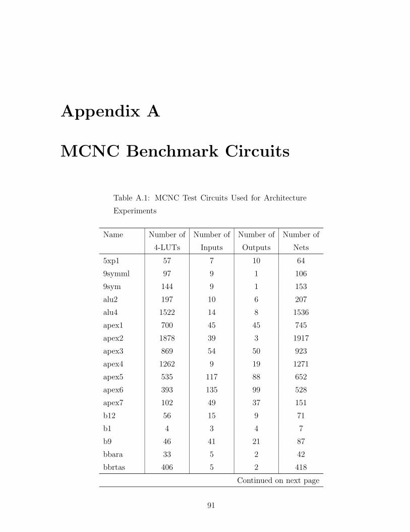
Appendix A
MCNC Benchmark Circuits
Table A.1: MCNC Test Circuits Used for Architecture
Experiments
Name Number of Number of Number of Number of
4-LUTs Inputs Outputs Nets
5xp1 57 7 10 64
9symml 97 9 1 106
9sym 144 9 1 153
alu2 197 10 6 207
alu4 1522 14 8 1536
apex1 700 45 45 745
apex2 1878 39 3 1917
apex3 869 54 50 923
apex4 1262 9 19 1271
apex5 535 117 88 652
apex6 393 135 99 528
apex7 102 49 37 151
b12 56 15 9 71
b1 4 3 4 7
b9 46 41 21 87
bbara 33 5 2 42
bbrtas 406 5 2 418
Continued on next page
91

Appendix A. MCNC Benchmark Circuits 92
Table A.1 – continued from previous page
Name Number of Number of Number of Number of
4-LUTs Inputs Outputs Nets
bbsse 64 8 7 76
bbtas 6 3 2 12
beecount 14 4 4 21
bigkey 1707 263 197 2194
bw 132 5 28 137
C1355 74 41 32 115
C17 2 5 2 7
C1908 145 33 25 178
C2670 259 233 64 492
C3540 431 50 22 481
C432 124 36 7 160
C499 74 41 32 115
C5315 620 178 123 798
C6288 527 32 32 559
C7552 739 207 107 946
C880 174 60 26 234
c8 39 28 18 67
cc 26 21 20 47
cht 55 47 36 102
clip 140 9 5 149
clma 8381 383 82 8797
cm138a 10 6 8 16
cm150a 14 21 1 35
cm151a 8 12 2 20
cm152a 6 11 1 17
cm162a 18 14 5 32
cm163a 11 16 5 27
cm42a 10 4 10 14
cm82a 4 5 3 9
Continued on next page
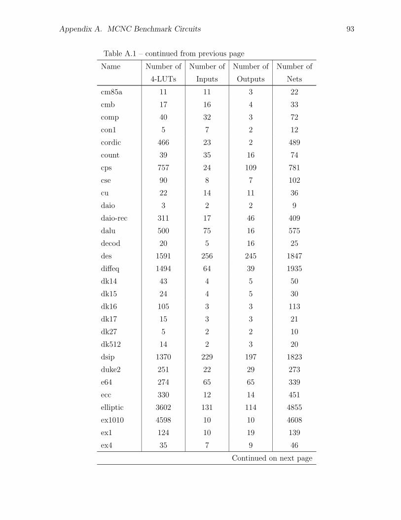
Appendix A. MCNC Benchmark Circuits 93
Table A.1 – continued from previous page
Name Number of Number of Number of Number of
4-LUTs Inputs Outputs Nets
cm85a 11 11 3 22
cmb 17 16 4 33
comp 40 32 3 72
con1 5 7 2 12
cordic 466 23 2 489
count 39 35 16 74
cps 757 24 109 781
cse 90 8 7 102
cu 22 14 11 36
daio 3 2 2 9
daio-rec 311 17 46 409
dalu 500 75 16 575
decod 20 5 16 25
des 1591 256 245 1847
diffeq 1494 64 39 1935
dk14 43 4 5 50
dk15 24 4 5 30
dk16 105 3 3 113
dk17 15 3 3 21
dk27 5 2 2 10
dk512 14 2 3 20
dsip 1370 229 197 1823
duke2 251 22 29 273
e64 274 65 65 339
ecc 330 12 14 451
elliptic 3602 131 114 4855
ex1010 4598 10 10 4608
ex1 124 10 19 139
ex4 35 7 9 46
Continued on next page

Appendix A. MCNC Benchmark Circuits 94
Table A.1 – continued from previous page
Name Number of Number of Number of Number of
4-LUTs Inputs Outputs Nets
ex4p 445 128 28 573
ex5p 1064 8 63 1072
ex6 60 6 8 69
example2 138 85 66 223
f51m 54 8 8 62
frg1 49 28 3 77
frg2 379 143 139 522
frisc 3539 20 116 4445
gcd 218 19 25 295
i10 995 257 224 1252
i1 21 25 13 46
i2 74 201 1 275
i3 46 132 6 178
i4 98 192 6 290
i5 88 133 66 221
i6 182 138 67 320
i7 203 199 67 402
i8 481 133 81 614
i9 376 88 63 464
inc 64 7 9 71
k2 519 45 45 564
keyb 103 8 2 116
lal 34 26 19 60
ldd 37 9 19 46
lion 3 3 1 8
majority 3 5 1 8
mark1 37 6 16 47
mc 7 4 5 13
misex1 21 8 7 29
Continued on next page

Appendix A. MCNC Benchmark Circuits 95
Table A.1 – continued from previous page
Name Number of Number of Number of Number of
4-LUTs Inputs Outputs Nets
misex2 49 25 18 74
misex3c 549 14 14 563
misex3 1397 14 14 1411
mm30a 467 34 30 591
mm4a 78 8 4 98
mm9a 142 13 9 182
mm9b 204 13 9 243
mult16a 57 18 1 91
mult16b 31 18 1 79
mult32a 116 34 1 182
mux 15 21 1 36
my-adder 47 33 17 80
o64 46 130 1 176
opus 50 6 6 60
pair 647 173 137 820
parity 5 16 1 21
parker1986 660 50 9 871
pcle 21 19 9 40
pcler8 35 27 17 62
pdc 4575 16 40 4591
ph-decod 219 4 10 278
planet1 266 8 19 280
planet 266 8 19 280
pm1 19 16 13 35
pma 85 9 8 99
rd53 12 5 3 17
rd73 83 7 3 90
rd84 157 8 4 165
rot 307 135 107 442
Continued on next page
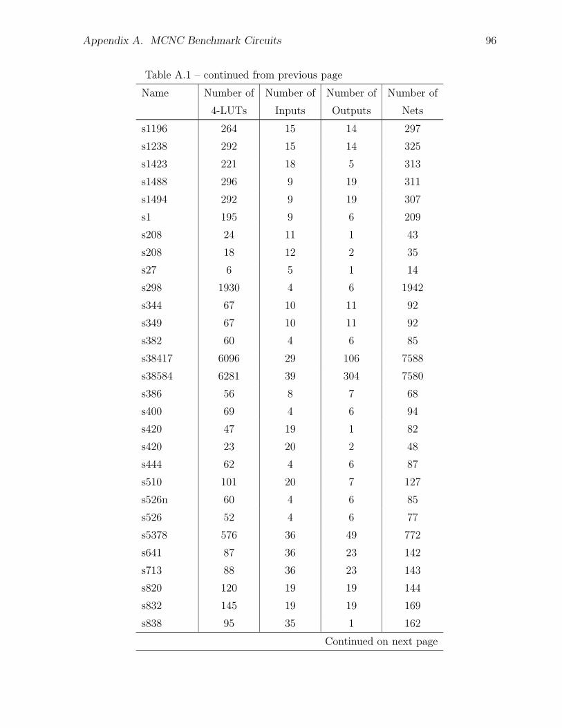
Appendix A. MCNC Benchmark Circuits 96
Table A.1 – continued from previous page
Name Number of Number of Number of Number of
4-LUTs Inputs Outputs Nets
s1196 264 15 14 297
s1238 292 15 14 325
s1423 221 18 5 313
s1488 296 9 19 311
s1494 292 9 19 307
s1 195 9 6 209
s208 24 11 1 43
s208 18 12 2 35
s27 6 5 1 14
s298 1930 4 6 1942
s344 67 10 11 92
s349 67 10 11 92
s382 60 4 6 85
s38417 6096 29 106 7588
s38584 6281 39 304 7580
s386 56 8 7 68
s400 69 4 6 94
s420 47 19 1 82
s420 23 20 2 48
s444 62 4 6 87
s510 101 20 7 127
s526n 60 4 6 85
s526 52 4 6 77
s5378 576 36 49 772
s641 87 36 23 142
s713 88 36 23 143
s820 120 19 19 144
s832 145 19 19 169
s838 95 35 1 162
Continued on next page
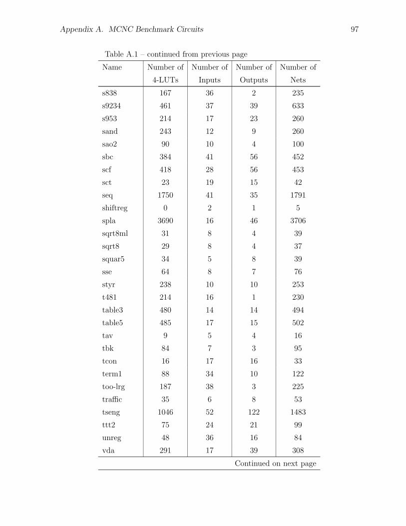
Appendix A. MCNC Benchmark Circuits 97
Table A.1 – continued from previous page
Name Number of Number of Number of Number of
4-LUTs Inputs Outputs Nets
s838 167 36 2 235
s9234 461 37 39 633
s953 214 17 23 260
sand 243 12 9 260
sao2 90 10 4 100
sbc 384 41 56 452
scf 418 28 56 453
sct 23 19 15 42
seq 1750 41 35 1791
shiftreg 0 2 1 5
spla 3690 16 46 3706
sqrt8ml 31 8 4 39
sqrt8 29 8 4 37
squar5 34 5 8 39
sse 64 8 7 76
styr 238 10 10 253
t481 214 16 1 230
table3 480 14 14 494
table5 485 17 15 502
tav 9 5 4 16
tbk 84 7 3 95
tcon 16 17 16 33
term1 88 34 10 122
too-lrg 187 38 3 225
traffic 35 6 8 53
tseng 1046 52 122 1483
ttt2 75 24 21 99
unreg 48 36 16 84
vda 291 17 39 308
Continued on next page

Appendix A. MCNC Benchmark Circuits 98
Table A.1 – continued from previous page
Name Number of Number of Number of Number of
4-LUTs Inputs Outputs Nets
vg2 67 25 8 92
x1 143 51 35 194
x2 17 10 7 27
x3 377 135 99 512
x4 194 94 71 288
xor5 2 5 1 7
z4ml 8 7 4 15

Appendix B
SRAM Programmer Verilog
Description
//// GILES Programmer// A v e r i l o g implementat ion t ha t can be used to program// a GILES genera ted FPGA// by Ian Kuon// Ju ly 2003// Updated throughout 2003//‘timescale 1 ns / 1 ns
//∗∗∗∗∗∗∗∗∗∗∗∗∗∗∗∗∗∗∗∗∗∗∗∗∗∗∗∗∗∗∗∗∗∗∗∗∗∗∗∗∗∗∗∗∗∗∗∗∗∗∗∗∗∗∗//// The f o l l ow i n g modules are j u s t b a s i c e lements// such as comparators , r e g i s t e r s and counters////∗∗∗∗∗∗∗∗∗∗∗∗∗∗∗∗∗∗∗∗∗∗∗∗∗∗∗∗∗∗∗∗∗∗∗∗∗∗∗∗∗∗∗∗∗∗∗∗∗∗∗∗∗∗∗
module s h i f t r e g ( c lk , s h i f t i n , data out , enable , r e s e t b ) ;
// synopsys s y n c s e t r e s e t ” r e s e t b ”parameter data width =10;parameter i n i t i a l i z a t i o n v a l u e =’b0 ;input c l k ;input s h i f t i n ;output [ data width −1:0] data out ;input enable ;
99

Appendix B. SRAM Programmer Verilog Description 100
input r e s e t b ;
reg [ data width −1:0] data out ;
always@ (posedge c l k )i f ( r e s e t b==0)
data out<=i n i t i a l i z a t i o n v a l u e ;else i f ( enable==1) begin
data out<=data out <<1;data out [0]<= s h i f t i n ;
end // i f ( enab l e==1)
endmodule // s h i f t r e g
module mux 2 1 (A, B, s e l , out ) ;
parameter data width =10;input [ data width −1:0] A, B;input s e l ;output [ data width −1:0] out ;
reg [ data width −1:0] out ;
always @(A or B or s e l )begin
case ( s e l )0 : out = A;1 : out = B;
// d e f a u l t : out <=A;endcase
end
endmodule // mux 2 1
module counter ( c lk , enable , r e s e t b , count ) ;
// synopsys s y n c s e t r e s e t ” r e s e t b ”parameter count width =2;
input c l k ;input enable ;
Appendix B. SRAM Programmer Verilog Description 101
input r e s e t b ;output [ count width −1:0] count ;
reg [ count width −1:0] count ;
always @(posedge c l k )i f ( r e s e t b == 0)
count <=0;else i f ( enable==1)
count<=count+1;
endmodule // counter
module comparator (A,B, eq ) ;
parameter comp width=2;input [ comp width −1:0] A,B;output eq ;
assign eq = A==B;
endmodule // comparator
module g i l e s programmer embedded sh i f t ( r e s e t b , c lk ,program ready , program enable , t o b i t s h i f t , t o wo rd sh i f t ,p rog c lk , prog c lk b , word enable , word enable b ,word f l op enab l e , b i t f l o p e n ab l e , data in , done l ine , d on e a l l );
// A l l the b i t s// f o r an en t i r e word l i n e must be programmed at once// b i t l i n e s// | |// −−−+−−−−−−+−−−−−−−−−− word l i n e// | |// −−−+−−−−−−+−−−−−−−−−−// | |//parameter b i t count =144;parameter word count =144;parameter b i t c oun t l o g 2 =8;
Appendix B. SRAM Programmer Verilog Description 102
parameter word count log2 =8;
input r e s e t b ;input c l k ;input data in ;input program enable ;
output t o b i t s h i f t ;output t o wo rd sh i f t ;output prog c l k ;output prog c l k b ;output word enable ;output word enable b ;output word f l op enab l e ;output b i t f l o p e n a b l e ;
output done l i n e ;output done a l l ;output program ready ;
wire [ b i t count −1:0] p r o g b i t s ;wire [ b i t c oun t l og2 −1:0] b i t s r e c e i v e d ;wire [ word count −1:0] words r ece ived ;wire b i t count enab l e ,
word count enable ;wire b i t compare r e su l t ,
word compare resu l t ;wire c oun t e r r e s e t b ;wire i d l e r e s e t b ;wire program ;
wire [ word count −1:0] z e r o s ;wire [ b i t c oun t l og2 −1:0] b i t count compare va l ;
wire [ word count −1:0 ] word count compare val ;wire b i t c o u n t e r r e s e t b ;
wire word sh i f t ;
assign b i t count compare va l=bi t count −1;

Appendix B. SRAM Programmer Verilog Description 103
//The compare va lue i s the l a s t word to be wr i t t en hence the//word count −1.assign word count compare val=1’b1<<(word count−1) ;
assign z e ro s =’b0 ;
assign c oun t e r r e s e t b=i d l e r e s e t b&r e s e t b ;
//Assign the s i g n a l s t h a t j u s t f l ow through the b l o c kassign prog c l k=c lk ;assign prog c l k b=˜c lk ;assign t o b i t s h i f t=data in ;assign word f l op enab l e=word count enable ;assign b i t f l o p e n a b l e=b i t c oun t enab l e ;
//Data w i l l be s h i f t e d in u n t i l the r e g i s t e r i s f u l l//which w i l l be known by us ing a counter . A s i n g l e word// l i n e w i l l then be programmed . As a f i r s t v e r s i on t h i s// w i l l s imply s t a r t a t word l i n e 0 a f t e r r e s e t and increment// in a loop .////
// S h i f t r e g i s t e r which s t o r e s the b i t s as they are r e c e i v eds h i f t r e g #(b i t count ) b i t s t o r e 0 ( . c l k ( c l k ) , . s h i f t i n (
da ta in ) , . data out ( p r o g b i t s ) ,. enable ( b i t c oun t enab l e ) , . r e s e t b (
r e s e t b ) ) ;// Some compi l e r s don ’ t seem to l i k e defparams// defparam b i t s t o r e 0 . da ta w id th=b i t c o un t ;
//Bit counter to know when we are ready to wr i t e a wordcounter #(b i t c oun t l o g 2 ) b i t c oun t 0 ( . c l k ( c l k ) , . enable (
b i t c oun t enab l e ) ,. r e s e t b ( b i t c o u n t e r r e s e t b ) ,. count ( b i t s r e c e i v e d ) ) ;
// defparam b i t c o un t 0 . count wid th=b i t c o u n t l o g 2 ;
//We need to r e s e t the count every time we wr i t e a wordassign b i t c o u n t e r r e s e t b=coun t e r r e s e t b & ( ! done l i n e ) ;
Appendix B. SRAM Programmer Verilog Description 104
//This comparator determines when we have r e c e i v ed a l l theb i t s
// defparam bi t compare 0 . comp width=b i t c o u n t l o g 2 ;comparator b i t compare 0 ( .A( b i t s r e c e i v e d ) , .B(
b i t count compare va l ) ,. eq ( b i t c ompa r e r e su l t ) ) ;
defparam bit compare 0 . comp width=b i t c oun t l o g 2 ;
//Word counter to know when the en t i r e dev i c e i s programmed//A s h i f t r e g i s t e r i s used in s t ead o f a counter because I
want// to avoid decoding numbers to the one hot r e p r e s en t a t i ons h i f t r e g word count 0 ( . c l k ( c l k ) , . s h i f t i n (1 ’ b0 ) , . data out (
words r ece ived ) ,. enable ( word count enable ) ,. r e s e t b ( c oun t e r r e s e t b ) ) ;
defparam word count 0 . data width=word count ;defparam word count 0 . i n i t i a l i z a t i o n v a l u e =’b01 ;
//The f l o p s f o r the s h i f t reg don ’ t have a r e s e t// so we must waste time i n i t i a l i z i n g them
assign t o wo rd sh i f t=word sh i f t ;assign word enable=program ;assign word enable b=˜program ;
//This comparator determines when we have r e c e i v ed a l l theb i t s
comparator word compare 0 ( .A( words r ece ived ) , .B(word count compare val ) ,
. eq ( word compare resu l t ) ) ;defparam word compare 0 . comp width=word count ;
// Con t r o l l e r which makes e v e r y t h i n g work t o g e t h e rg i l e s p r og r am con t r o l embedded sh i f t g i l e s c o n t r o l ma i n (
. c l k ( c l k ) ,
. b i t c ompa r e r e su l t ( b i t c ompa r e r e su l t ) ,
. word compare resu l t ( word compare resu l t ) ,
. b i t c oun t enab l e ( b i t c oun t enab l e ) ,
. word count enable ( word count enable ) ,

Appendix B. SRAM Programmer Verilog Description 105
. perform program ( program ) ,
. i d l e r e s e t b ( i d l e r e s e t b ) ,
. r e s e t b ( r e s e t b ) ,
. program enable ( program enable ) ,
. d one l i n e ( done l i n e ) ,
. d on e a l l ( d on e a l l ) ,
. program ready ( program ready ) ,
. wo rd sh i f t ( wo rd sh i f t ) ) ;
endmodule // gi les programmer mainmodule g i l e s p r og r am con t r o l embedded sh i f t ( c lk ,
b i t c ompare r e su l t ,word compare result ,b i t count enab l e , word count enable ,perform program , i d l e r e s e t b , r e s e t b ,program enable , done l ine , done a l l ,program ready , wo rd sh i f t ) ;
input c l k ;input b i t compare r e su l t , word compare resu l t ;output b i t count enab l e , word count enable ;output perform program , i d l e r e s e t b ;input r e s e t b ;input program enable ;output done l ine , d on e a l l ;output program ready ;output word sh i f t ;
reg b i t count enab l e , word count enable ;reg done l ine , d on e a l l ;reg perform program , i d l e r e s e t b ;reg program ready ;reg word sh i f t ;
parameter STATE SIZE = 3 ;parameter IDLE = ’ b000 ;parameter INITIALIZE = ’ b111 ;parameter PREPARE TO PROGRAM = ’ b110 ;parameter BIT RECEIVE = ’ b001 ;parameter BIT PROGRAM = ’ b010 ;parameter BIT PROGRAM PRE WAIT = ’ b101 ;parameter BIT PROGRAM POST WAIT = ’ b100 ;
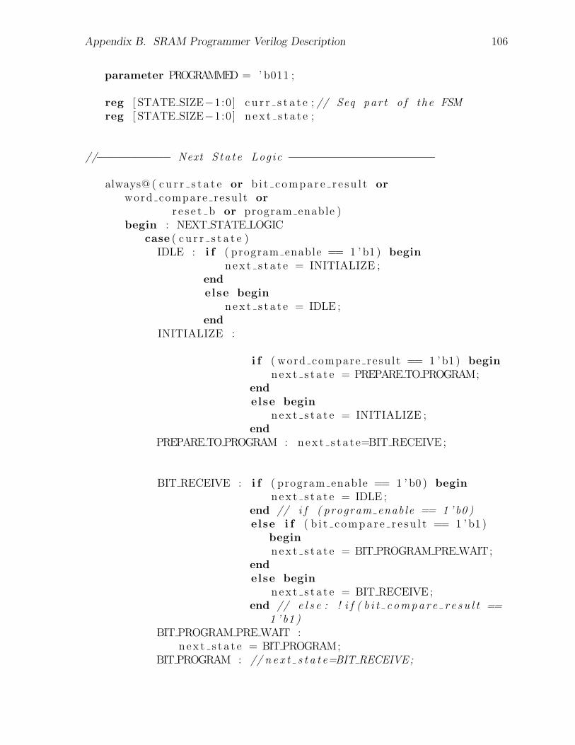
Appendix B. SRAM Programmer Verilog Description 106
parameter PROGRAMMED = ’ b011 ;
reg [ STATE SIZE−1:0] c u r r s t a t e ; // Seq par t o f the FSMreg [ STATE SIZE−1:0] n ex t s t a t e ;
//−−−−−−−−−−− Next S ta t e Logic −−−−−−−−−−−−−−−−−−−−−−
always@ ( c u r r s t a t e or b i t c ompa r e r e su l t orword compare resu l t or
r e s e t b or program enable )begin : NEXT STATE LOGIC
case ( c u r r s t a t e )IDLE : i f ( program enable == 1 ’ b1 ) begin
nex t s t a t e = INITIALIZE ;endelse begin
nex t s t a t e = IDLE ;end
INITIALIZE :
i f ( word compare resu l t == 1 ’ b1 ) beginnex t s t a t e = PREPARE TO PROGRAM;
endelse begin
nex t s t a t e = INITIALIZE ;end
PREPARE TO PROGRAM : nex t s t a t e=BIT RECEIVE ;
BIT RECEIVE : i f ( program enable == 1 ’ b0 ) beginnex t s t a t e = IDLE ;
end // i f ( program enable == 1 ’ b0 )else i f ( b i t c ompa r e r e su l t == 1 ’ b1 )
beginnex t s t a t e = BIT PROGRAM PRE WAIT;
endelse begin
nex t s t a t e = BIT RECEIVE ;end // e l s e : ! i f ( b i t c ompa r e r e s u l t ==
1 ’ b1 )BIT PROGRAM PRE WAIT :
n ex t s t a t e = BIT PROGRAM;BIT PROGRAM : // n e x t s t a t e=BIT RECEIVE;
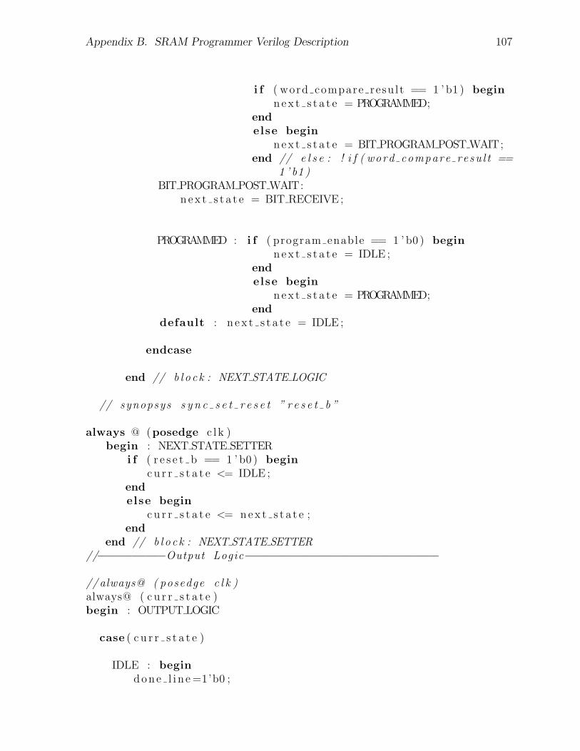
Appendix B. SRAM Programmer Verilog Description 107
i f ( word compare resu l t == 1 ’ b1 ) beginnex t s t a t e = PROGRAMMED;
endelse begin
nex t s t a t e = BIT PROGRAM POST WAIT;end // e l s e : ! i f ( word compare resu l t ==
1 ’ b1 )BIT PROGRAM POST WAIT:
n ex t s t a t e = BIT RECEIVE ;
PROGRAMMED : i f ( program enable == 1 ’ b0 ) beginnex t s t a t e = IDLE ;
endelse begin
nex t s t a t e = PROGRAMMED;end
default : n e x t s t a t e = IDLE ;
endcase
end // b l o c k : NEXT STATE LOGIC
// synopsys s y n c s e t r e s e t ” r e s e t b ”
always @ (posedge c l k )begin : NEXT STATE SETTER
i f ( r e s e t b == 1 ’ b0 ) beginc u r r s t a t e <= IDLE ;
endelse begin
c u r r s t a t e <= nex t s t a t e ;end
end // b l o c k : NEXT STATE SETTER//−−−−−−−−−−Output Logic−−−−−−−−−−−−−−−−−−−−−−−−−−−−−
//always@ ( posedge c l k )always@ ( c u r r s t a t e )begin : OUTPUT LOGIC
case ( c u r r s t a t e )
IDLE : begindone l i n e =1’b0 ;

Appendix B. SRAM Programmer Verilog Description 108
don e a l l =1’b0 ;perform program=1’b0 ;i d l e r e s e t b =1’b0 ;b i t c oun t enab l e =1’b0 ;word count enable=1’b0 ;program ready=1’b1 ;wo rd sh i f t =1’b0 ;
endINITIALIZE : begin
done l i n e =1’b0 ;d on e a l l =1’b0 ;perform program=1’b0 ;i d l e r e s e t b =1’b1 ;b i t c oun t enab l e =1’b0 ;word count enable=1’b1 ;program ready=1’b0 ;wo rd sh i f t =1’b0 ;
endPREPARE TO PROGRAM : begin
done l i n e =1’b0 ;d on e a l l =1’b0 ;perform program=1’b0 ;i d l e r e s e t b =1’b0 ;b i t c oun t enab l e =1’b0 ;word count enable=1’b1 ;program ready=1’b0 ;wo rd sh i f t =1’b1 ;
endBIT RECEIVE : begin
done l i n e =1’b0 ;d on e a l l =1’b0 ;perform program=1’b0 ;i d l e r e s e t b =1’b1 ;b i t c oun t enab l e =1’b1 ;word count enable=1’b0 ;program ready=1’b1 ;wo rd sh i f t =1’b0 ;
endBIT PROGRAM PRE WAIT : begin
done l i n e =1’b1 ;d on e a l l =1’b0 ;perform program=1’b0 ;i d l e r e s e t b =1’b1 ;b i t c oun t enab l e =1’b0 ;word count enable=1’b0 ;

Appendix B. SRAM Programmer Verilog Description 109
program ready=1’b0 ;wo rd sh i f t =1’b0 ;
endBIT PROGRAM : begin
done l i n e =1’b1 ;d on e a l l =1’b0 ;perform program=1’b1 ;i d l e r e s e t b =1’b1 ;b i t c oun t enab l e =1’b0 ;word count enable=1’b1 ;program ready=1’b0 ;wo rd sh i f t =1’b0 ;
endBIT PROGRAM POST WAIT : begin
done l i n e =1’b1 ;d on e a l l =1’b0 ;perform program=1’b0 ;i d l e r e s e t b =1’b1 ;b i t c oun t enab l e =1’b0 ;word count enable=1’b0 ;program ready=1’b0 ;wo rd sh i f t =1’b0 ;
endPROGRAMMED : begin
done l i n e =1’b0 ;d on e a l l =1’b1 ;perform program=1’b0 ;i d l e r e s e t b =1’b1 ;b i t c oun t enab l e =1’b0 ;word count enable=1’b0 ;program ready=1’b1 ;wo rd sh i f t =1’b0 ;
enddefault : begin
done l i n e =1’b0 ;d on e a l l =1’b0 ;perform program=1’b0 ;i d l e r e s e t b =1’b0 ;b i t c oun t enab l e =1’b0 ;word count enable=1’b0 ;program ready=1’b0 ;wo rd sh i f t =1’b0 ;
endendcase

Appendix B. SRAM Programmer Verilog Description 110
//end
end // End Of Block OUTPUT LOGIC
endmodule // g i l e s p r o g r am con t r o l embedd ed s h i f t
Bibliography
[1] Yoshiko Hara. Sony’s Makimoto says FPGAs ’a must’ in consumer electronics.EE Times, June 2003. Available online at: http://www.eetimes.com/story/
OEG20030627S0044.
[2] Xilinx. ASIC Cost Estimator: WebACE. http://www.xilinx.com/products/
webace/index.htm, Accessed May 2004.
[3] Steven Brown, Robert Francis, Jonathan Rose, and Zvonko Vranesic. Field-Programmable Gate Arrays. Kluwer Academic Publishers, 1992.
[4] Ketan Padalia, Ryan Fung, Mark Bourgeault, Aaron Egier, and Jonathan Rose.Automatic transistor and physical design of FPGA tiles from an architectural speci-fication. In Proceedings of the 2003 ACM/SIGDA eleventh international symposiumon Field programmable gate arrays, pages 164–172. ACM Press, 2003.
[5] Ketan Padalia. Automatic transistor-level design and layout placement of FPGAlogic and routing from an architectural specification. Bachelor’s thesis, Universityof Toronto, 2001.
[6] Ryan Fung. Optimization of transistor-level floorplans for field-programmable gatearrays. Bachelor’s thesis, University of Toronto, 2002.
[7] Mark Bourgeault, Joshua Slavkin, and Chris Sun. Automatic transistor-level designand layout of FPGAs. Bachelor’s thesis, University of Toronto, 2002.
[8] Vaughn Betz, Jonathan Rose, and Alexander Marquardt. Architecture and CAD forDeep-Submicron FPGAs. Kluwer Academic Publishers, 1999.
[9] Xilinx. Virtex-II platform complete data sheet. http://direct.xilinx.com/
bvdocs/publications/ds031.pdf, March 2004. DS031.
[10] Altera. Stratix II device handbook. http://www.altera.com/literature/hb/
stx2/stratix2_handbook.pdf, 2004. ver SII5V1-1.0.
[11] Stuart McCracken. Reconfigurable device interconnect test and diagnosis time re-duction. Master’s of engineering thesis, McGill University, 2002.
111
Bibliography 112
[12] Noha Kafafi, Kimberly Bozman, and Steven J. E. Wilton. Architectures and algo-rithms for synthesizable embedded programmable logic cores. In Proceedings of the2003 ACM/SIGDA eleventh international symposium on Field programmable gatearrays, pages 3–11. ACM Press, 2003.
[13] Varghese George. Low Energy Field-Programmable Gate Array. PhD thesis, Uni-versity of California, Berkeley, 2000.
[14] Danesh Tavana, Wilson K. Yee, and Victor A. Holen. FPGA architecture withrepeatable tiles including routing matrices and logic matrices, October 1997. USPatent 5,682,107.
[15] Bai Nguyen, Om P. Agrawal, Bradley A. Sharpe-Giesler, Jack T. Wong, Herman MChang, and Giap H. Tran. Tileable and compact layout for super variable grainblocks within FPGA device, November 2000. US Patent 6,154,051.
[16] Shawn Phillips and Scott Hauck. Automatic layout of domain-specific reconfigurablesubsystems for system-on-a-chip. In Proceedings of the 2002 ACM/SIGDA tenthinternational symposium on Field-programmable gate arrays, pages 165–173. ACMPress, 2002.
[17] Paul Chow, Soon Ong Seo, Jonathan Rose, Kevin Chung, Gerar Paez-Monzon,and Immanuel Rahardja. The design of a SRAM-based field programmable gatearray-part ii: Circuit design and layout. IEEE Transactions on Very Large ScaleIntegration (VLSI) Systems, 7(3):321–330, Sept 1999.
[18] Jeremy Brown, Derrick Chen, Ian Eslick, Edward Tau, and Andre DeHon. DELTA:Prototype for a first-generation dynamically programmable gate array. TechnicalReport Transit Note 115, Massachusetts Institute of Technology, 1995.
[19] Vaughn Betz. Architecture and CAD for Speed and Area Optimization of FPGAs.PhD thesis, University of Toronto, 1998.
[20] Vaughn Betz and Jonathan Rose. Automatic generation of FPGA routing architec-tures from high-level descriptions. In Proceedings of the 2000 ACM/SIGDA eighthinternational symposium on Field programmable gate arrays, pages 175–184. ACMPress, 2000.
[21] Vaughn Betz and Jonathan Rose. Automatic generation of programmable logicdevice architectures, October 2003. US Patent 6,631,510.
[22] Aaron Egier. Using/building automated transistor and physical design of fpgas.Master’s thesis, University of Toronto, In preparation.
[23] Cadence. Cadence IC Craftsman Router, 2003. Currently called the Cadence ChipAssembly Router with datasheet at: http://www.cadence.com/datasheets/4886_virtuosoCAR_DSfnl.pdf.
Bibliography 113
[24] Xilinx. Virtex-E 1.8v field programmable gate arrays production product specifica-tion, July 2002. DS022-1 (v2.3).
[25] Altera. APEX 20K data sheet, January 2004. ver 5.0.
[26] Xilinx. Virtex series configuration architecture user guide, September 2000.XAPP151 (v1.5).
[27] T. Uehara and W. M. Van Cleemput. Optimal layout of CMOS functional arrays.IEEE Transactions on Computers, C-30:305–312, May 1981.
[28] Yung-Ching Hsieh, Chi-Yi Hwang, Youn-Long Ling, and Yu-Chin Hsu. LiB: ACMOS cell compiler. IEEE Transactions on Computer-Aided Design of integratedCircuits and Systems, 10(8):994–1005, August 1991.
[29] Chi Yi Hwang, Yung Ching Hsieh, Youn-Long Lin, and Yu-Chin Hsu. An efficientlayout style for two-metal CMOS leaf cells and its automatic synthesis. IEEE Trans-actions on Computer-Aided Design of Integrated Circuits and Systems, 12(3):410–424, March 1993.
[30] Tatjana Serdar and Carl Sechen. AKORD: transistor level and mixed transistor/gatelevel placement tool for digital data paths. In IEEE/ACM International Conferenceon Computer-Aided Design, 1999. Digest of Technical Papers, pages 91–97, Novem-ber 1999.
[31] T. Serdar and C. Sechen. Automatic datapath tile placement and routing. InProceedings of the conference on Design, automation and test in Europe, pages 552–559. IEEE Press, 2001.
[32] C. A. T. Salama. ECE1388 class notes. 2002.
[33] Jan M. Rabaey. Digital Integrated Circuits A Design Perspective. Prentice Hall,1996.
[34] Michael John Sebastian Smith. ASICs... the book. Addison-Wesley PublishingCompany, 1997. Available online at: http://www-ee.eng.hawaii.edu/~msmith/
ASICs/HTML/ASICs.htm.
[35] Artisan components. http://www.artisan.com.
[36] Virtual Silicon Technology. Diplomat-18 standard cell library, 2003. http://www.
virtual-silicon.com/view_press_release.cfm?prid=53.
[37] Cadence. Design planner, 2003. http://www.cadence.com/company/pr/
photogallery/prod_logic_planner.html.
[38] Cadence. Silicon ensemble DSM, 2003. http://www.cadence.com/company/pr/
photogallery/prod_silicon.html.

Bibliography 114
[39] Synopsys. Design compiler. Product Description available at: http://www.
synopsys.com/products/logic/design_compiler.html.
[40] William J. Dally and Andrew Chang. The role of custom design in ASIC chips. InProceedings of the 37th Design Automation Conference, pages 643–647. ACM Press,2000.
[41] Xilinx. FPGA editor, 2003. http://toolbox.xilinx.com/docsan/xilinx5/help/fpga_editor/fpga_editor.htm.
[42] Steven P. Young. Six-input multiplexer with two gate levels and three memory cells,April 1998. US Patent 5,744,995.
[43] Steven P. Young. FPGA layout for a pair of six input multiplexers, October 1999.US Patent 5,962,881.
[44] T. Bauer. Lookup tables which double as shift registers, March 1999. US Patent5,889,413.
[45] A. T. Nguyen. High-speed flip-flop operable at very low voltage levels with set andreset capability, December 2002. US Patent 6,501,315.
[46] Avant! Star-HSPICE, 1997.
[47] S. N. Adya, I. L. Markov, and P. G. Villarrubia. On whitespace and stability inmixed-size placement and physcial synthesis. In Proceedings of the 2003 Interna-tional Conference on Computer Aided Design, pages 311–318, 2003.
[48] Tom Burd. Low power CMOS library design methodology. Master’s thesis, Uni-versity of California, Berkeley, 1995. Available on-line at: http://bwrc.eecs.
berkeley.edu/Publications/theses/low.power.CMOS.library.MS/.
[49] SGS-Thompson Microelectronics. CB45000 Series HCMOS6 Standard Cells, March1998. http://www.st.com/.
[50] Simon So. Automatic layout of FPGA tiles using one-layer metal cells. Bachelor’sthesis, University of Toronto, 2003.
[51] Canadian Microelectronics Corporation. http://www.cmc.ca.
[52] Arno Wagner. Berkeley logic interchange format (BLIF). http://www.bdd-portal.org/docu/blif/, Decemeber 1998.
[53] Alexander R. Marquardt. Cluster-based architecture, timing-driven packing andtiming-driven placement for FPGAs. Master of applied science thesis, University ofToronto, 1999.
[54] Paul Chow, Soon Ong Seo, Jonathan Rose, Kevin Chung, Gerar Paez-Monzon, andImmanuel Rahardja. The Design of a SRAM-based Field Programmable Gate Array-Part I: Architecture. IEEE Transactions on Very Large Scale Integration (VLSI)Systems, 7(2):191–197, June 1999.
Bibliography 115
[55] David Lewis, Vaughn Betz, David Jefferson, Andy Lee, Chris Lane, Paul Leventis,Sandy Marquardt, Cameron McClintock, Bruce Pedersen, Giles Powell, SrinivasReddy, Chris Wysocki, Richard Cliff, and Jonathan Rose. The StratixTM routing andlogic architecture. In Proceedings of the 2003 ACM/SIGDA eleventh internationalsymposium on Field programmable gate arrays, pages 12–20. ACM Press, 2003.
[56] Elias Ahmed and Jonathan Rose. The effect of LUT and cluster size on deep-submicron FPGA performance and density. In Proceedings of the 2000 ACM/SIGDAeighth international symposium on Field programmable gate arrays, pages 3–12.ACM Press, 2000.
[57] Altera. MAX II device handbook. http://www.altera.com/literature/hb/max2/max2_mii5v1.pdf, March 2004. ver MII5V1-1.0.
[58] Xilinx. The programmable logic data book, 1986. First Edition.
[59] A. El Gamal. Two-dimensional stochastic model for interconnections in master sliceintegrated circuits. IEEE Transactions on Computer Aided Design of IntegratedCircuits and Systems, CAS-28(2):127–138, February 1981.
[60] LGSynth93 MCNC Benchmarks. http://www.eecg.toronto.edu/~lemieux/
sega/ccts_blif.tar.gz, Accessed 2003.
[61] Cadence. Physically Knowledgeable Synthesis (PKS). Product Description availableat: http://www.cadence.com/datasheets/pks.pdf.
[62] John Mahoney. CMOS power-on reset circuit, May 1988. US Patent 4746822.
[63] Sergey Y. Shumarayev and Thomas H. White. Integrated circuit devices with powersupply detection circuitry, April 2003. US Patent 6549032.
[64] Ronald J. Mack, Derek R. Curd, Sholeh Diba, Napolean W. Lee, Kameswara K. Rao,and Mihai G. Statovici. Reset circuit for programmable logic device, November 1997.US Patent 5,962,881.
[65] P. Leventis, M. Chan, D. Lewis, B. Nouban, G. Powell, B. Vest, M. Wong, R. Xia,and J. Costello. Cyclone: a low-cost, high-performance FPGA. In Proceedings of theIEEE 2003 Custom Integrated Circuits Conference, pages 49–52, September 2003.
[66] Cadence. NC-Verilog. Product Description available at: http://www.cadence.com/products/functional_ver/nc-verilog/index.aspx.
[67] Synopsys. Nanosim. Product Description available at: http://www.synopsys.com/products/mixedsignal/nanosim/nanosim.html.
[68] Synopsys. Nanosim frequently asked questions. http://www.synopsys.com/
products/mixedsignal/nanosim/nanosim_faqs.html, April 2004.
[69] Cadence. Cadence IC design tools, 2000. 4.4.6.100.29.