Embed Size (px)
Citation preview

This article was originally published in a journal published byElsevier, and the attached copy is provided by Elsevier for the
author’s benefit and for the benefit of the author’s institution, fornon-commercial research and educational use including without
limitation use in instruction at your institution, sending it to specificcolleagues that you know, and providing a copy to your institution’s
administrator.
All other uses, reproduction and distribution, including withoutlimitation commercial reprints, selling or licensing copies or access,
or posting on open internet sites, your personal or institution’swebsite or repository, are prohibited. For exceptions, permission
may be sought for such use through Elsevier’s permissions site at:
http://www.elsevier.com/locate/permissionusematerial
Autho
r's
pers
onal
co
py
Electric Power Systems Research 77 (2007) 721–729
Control system design for VSC transmission
Dragan Jovcic a,∗, Lisa Lamont b,1, Keith Abbott c,2
a Engineering Department, University of Aberdeen, Aberdeen, Scotland AB23 3UE, UKb Electrical and Mechanical Engineering, University of Ulster, Newtownabbey BT37 OQB, UK
c Simulation and Studies, AREVA T & D, P.O. Box 27, Stafford ST17 4LN, UK
Received 22 June 2005; received in revised form 6 April 2006; accepted 19 June 2006Available online 4 August 2006
Abstract
This paper investigates a suitable control system for a DC transmission system based on voltage source converters (VSC). Each of the two VSCconverters has two control inputs and the four control channels on a VSC transmission system offer potential for a versatile control. However, themain challenge is the dynamic interaction among the control loops. It is proposed in this study that the overall system stability and good robustnessshould be achieved with two high-gain feedback loops, one at each converter. Eigenvalue and robustness analysis with MATLAB software showsthat the best fast feedback signals are inverter DC voltage and rectifier AC voltage q component. The slow controller consists of three PI controllersthat regulate: rectifier AC voltage, inverter AC voltage and the DC power. The VSC transmission control under fault conditions is achieved witha separate controller that takes over system control for fault-level currents. The fault controller regulates the local DC currents at each converter.The proposed controller is tested using PSCAD/EMTDC for a wide range of small-signal step inputs and the design performance is confirmed.The design is also tested for typical fault scenarios on AC and DC side to verify the fault controller operation.© 2006 Elsevier B.V. All rights reserved.
Keywords: VSC transmission; State-space methods; Thyristor converters; Root loci; Eigenvalues
1. Introduction
A voltage source converters (VSC) transmission system isgenerally similar to its predecessor HVDC transmission systemwhere the main difference is the use of voltage source convert-ers instead of line commutated converters (LCC). Because ofthe semiconductor technology constraints, VCS transmissionis at present limited to lower power (around 300 MW), but ithas already been implemented in a number of projects and it islikely to be further employed with higher voltage levels and inwider application areas [1]. The main advantage of VSC powertransmission is the high controllability, the ability to controlindependently active and reactive power at each terminal and thepossibility for linking with dead networks. These characteristicsmake VSC transmission attractive in many applications like theemerging interconnection with renewable energy sources. The
∗ Corresponding author. Tel.: +44 1224 272 336.E-mail addresses: [email protected] (D. Jovcic), [email protected]
(L. Lamont), [email protected] (K. Abbott).1 Tel.: +44 2890 368565.2 Tel.: +44 1785 257111.
disadvantages are known as higher power losses and higher cap-ital cost compared with conventional HVDC [1,2].
The converter topologies and their firing controls are in thedevelopment stage at many research centers, but it is widelybelieved that some form of pulse width modulation (PWM) con-trol with two control inputs will normally be used. From a controlsystem standpoint, a complete VSC transmission system hasfour control inputs, namely modulation signal magnitude andangle at each of the two converter stations. Because of the stronginteractions among the control channels, it is a truly non-linearmultiple-input multiple-output (MIMO) system.
Refs. [3,4] propose a method for controlling VSC transmis-sion based on a decoupling controller at each converter station.These methods use fast-feedback to linearise, decouple and sim-plify the feedback dynamics for d and q axis currents. The d–qcurrent control reference inputs are further used for implement-ing P–V (or P–Q, or VDC–Q) control strategies at higher controllevel. Ref. [5] discusses the shortcomings of current measure-ment lag and further improves decoupling controller using aninner predictive control loop (for a UPFC test system). Thepossible issues with controllers [3–5] in VSC transmission areidentified:
0378-7796/$ – see front matter © 2006 Elsevier B.V. All rights reserved.doi:10.1016/j.epsr.2006.06.011

Autho
r's
pers
onal
co
py
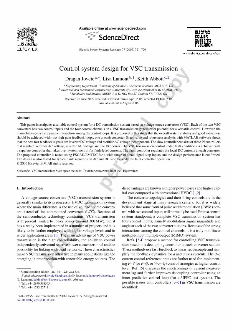
722 D. Jovcic et al. / Electric Power Systems Research 77 (2007) 721–729
Fig. 1. VSC test system schematic.
• Feedback linearisation/decoupling assumes that d–q axis cur-rents and DC voltage signals are available at the bandwidthhigher than the main control loops. In practice, these mea-surements are dependent on phase locked loop (PLL) outputand they are noise contaminated which reduces the frequencyrange for accurate measurements. Consequently, this slowsthe main control loops. In ref. [5] predictive current controllerimproves speed but only for the reference inputs, the distur-bance inputs rely on the current measurements.
• The control system in ref. [4] operates at three levels: at thefastest level is the feedback linearisation, then the main ACcurrent loops and the DC voltage is the slowest outer controlloop. Since the DC voltage is controlled in the outer controlloop, during disturbances it can have poor responses in termsof overshooting and rise/settling times. On the other hand,DC voltage control is very important with VSC convertersbecause of balancing issues since they are currently built oflarge number of small semiconductor units in series connec-tion.
• The same current controller is used for system protectionunder faults. The current controller can regulate fault cur-rents very well, but the control gains for fault conditions aredetuned to enable equally satisfactory small-signal dynamics.
• Such controller design considers only the local converterdynamics. The dynamics of the DC line or the interactionsbetween the two converters, which are important with VSCtransmission, are not considered. This implies larger over-shooting and slower responses as shown in ref. [3].
The aim of this study is to develop a fast VSC transmis-sion controller with good DC voltage transient behavior at bothconverters, which also guarantees good stability and robustnessproperties. The controller should further enable current and volt-age control during faults and fast fault recoveries.
The design is based on a small-signal linearised VSC trans-mission model developed earlier on MATLAB platform [6]. It is
also desired to fully test the design for wide range of step inputs(reference and disturbance) and also for a range of typical faultscenarios, on a more accurate non-linear simulator.
The paper firstly reviews the analytical model for VSC trans-mission. The small signal design is presented in details in Sec-tions 3–5, and the fault controller in Section 6. The controller istested in Section 7.
2. The test system and modeling
The test system and the analytical MATLAB model aredescribed in ref. [6] and only the summary is given here.
The test system is a 300 MW bi-pole VSC HVDC where onlyone pole (150 MW) is studied for simplicity. The system con-sists of a rectifier and inverter equivalent AC systems, the DCcircuit and the controller as shown in Fig. 1, where the param-eters are given in Appendix A. Each AC system has a typicalshort circuit level MVA of SCL = V 2
s /zth = 10, correspondingto short circuit ratio SCR = SCL/PDC = 6.6 in the nominal config-uration, and R/X = 0.26. The DC system corresponds to a 100 kmcable and includes the DC side capacitors, which are optimizedwith respect to the allowed DC voltage ripple. The controllermodel also includes a linearised PLL model at each converterstation.
The converters are two-level with bipolar PWM firing sig-nal generation. The PWM frequency ratio is 21. The MATLABmodel is a small-signal dynamic model linearised around thesteady state. The model consists of three individual units: ACrectifier system, AC inverter system and the DC circuit thatincludes all control systems. Each of these subsystems is anindependent state-space model and they are linked through thestate-space input–output matrices. This model enables eigen-value and frequency domain studies for the overall system in awide frequency domain. In ref. [6], the model accuracy is con-firmed against non-linear simulation on PSCAD/EMTDC [7]platform, for a range of input steps.
Table 1Control system input and output pairing
Input Output
Rectifier modulation signal magnitude Mmr Rectifier AC voltage magnitude VACR
Rectifier modulation signal angle Mfir Rectifier DC power PDCR
Inverter modulation signal magnitude Mmi Inverter AC voltage magnitude VACI
Inverter modulation signal angle Mfii Inverter DC voltage VDCI

Autho
r's
pers
onal
co
py
D. Jovcic et al. / Electric Power Systems Research 77 (2007) 721–729 723
Fig. 2. VSC transmission controller structure.
3. VSC transmission controller structure
The VSC transmission system is viewed as a multivariablefour-input four-output plant. The control inputs and the systemoutputs are paired as it is shown in Table 1.
If a PI control is used with each of these control loops it ispossible to achieve decoupled steady-state control and outputregulation as it is shown in ref. [6]. The dynamic performanceof such control system is however very poor, because of thestrong interactions among the control loops. Only one of thecontrol loops in such controller can have high gains and fastperformance, whereas the other variables have large overshoot-ings and long settling times. Because of the interactions, evenmodest gains lead to instabilities.
While the designs in refs. [3–5] concentrate on decouplingthe two controllers at each converter, from HVDC systemviewpoint this is a “local approach” since it neglects the DCline dynamics and the interactions between the two conver-ters.
An HVDC system with the two connecting AC systems canbe viewed as a dynamic system consisting of two coupled sub-systems, i.e. the rectifier and the inverter system. The dynamicinteractions between these two systems have important effect onVSC transmission dynamics and should be studied in controllerdesign. To enable good robustness and disturbance rejection ateach AC system, it is necessary to have a high-gain feedbackcontroller at each converter station, as shown in the study forconventional HVDC in ref. [8]. The design in this research isdirected primarily on resolving interactions between the twoconverters by considering dominant dynamics of the overallAC–DC–AC system.
The proposed controller structure is presented in Fig. 2. Thereis a high-gain fast controller at rectifier converter that rejectsrectifier side disturbances, and a fast inverter controller thatimproves inverter side stability. The main design effort is there-fore focused on developing structure and parameters of thesetwo loops in such way that they do not negatively interact.
4. Fast controller design
The fast controller has crucial influence on the stability,and the primary design goals are: good stability margins, goodrobustness for AC parameter changes at each AC system, andhigh performance regulation of the DC voltage. This designapproach considers dynamics of the overall AC–DC–AC sys-tem, in developing the controller. We note that the consideredAC–DC–AC system is complex, multivariable, higher order sys-tem (model is of 34th order), and also it is difficult to transmiton-line signals between rectifier and inverter considering thatthe length of DC line can be very large. These considerationstogether with high converter harmonics make the application ofconventional advanced control theories, like LQG or Hinf, verydifficult.
Because of importance of accurate DC voltage control, theDC voltage controller at inverter side is designed firstly. The PIcontroller design rules are used (assuming all other loops aredisconnected). The best achievable location of eigenvalues witha single PI controller is shown in Fig. 3 as diamonds. In thisfigure, only several most dominant eigenvalues are shown forsimplicity. We can observe that the eigenvalues (diamonds) onbranches A and B have poor damping and this will lead to lowquality dynamic properties.

Autho
r's
pers
onal
co
py
724 D. Jovcic et al. / Electric Power Systems Research 77 (2007) 721–729
Fig. 3. Root locus with stabilizing VACRq feedback. Diamonds represent openloop eigenvalues (VDCI control only).
At the next step, a rectifier fast controller is added, which isimportant for eliminating rectifier side disturbances. An addi-tional fast feedback loop at rectifier side is designed using rootlocus rules and the robustness indicators. We firstly create thelist of candidate rectifier feedback signals and examine the sys-tem performance for each candidate signal assuming a low orderfeedback controller. A particular attention is paid to the feedbacksignal selection at rectifier side in order to avoid complex high-order controllers. The candidate feedback signals are all locallyavailable variables at the rectifier converter, namely: the twocomponents of AC voltage and AC current, active and reactivepower, and DC side voltages and currents. All combinations ofthe ten outputs with each of the two rectifier control inputs areevaluated and compared. Considering the primary design goals,the analysis is centered on eigenvalue positioning and systemrobustness criteria, but the input and disturbance time domainresponses are also monitored. The goal is to move the two dom-inant eigenvalue pairs in Fig. 3 lying on the branches A andB, which are denoted by diamonds, to the left region with bet-ter damping. A systematic analysis with all candidate signalsis carried and the results show that none of the 20 input–outputcombinations gives satisfactory improvement. However, the bestfeedback signal is the rectifier AC voltage q component (VACRq)with rectifier modulation magnitude (Mmr), which gives rootlocus as shown in Fig. 3. This signal is selected for feed-back since it improves the position of the dominant eigenvalues(branch A), however, the improvement is modest and the eigen-values on the branch B deteriorate.
To stabilize the high frequency root locus and improve tran-sient performance a zero is added in the rectifier fast controller,represented by the lead compensator in Fig. 2. A zero in the feed-back transfer function increases the angles for asymptotes in theroot locus [9], thus moving roots to stable region. As the result,the final root locus is shown in Fig. 4. We can see that the domi-nant oscillatory mode (branch A′) has much better damping andalso other modes have improved dynamics. Most importantlyhowever because of the good direction of root locus branches itis possible to use high-gain rectifier feedback, which improvesrobustness.
Fig. 4. Root locus with stabilizing VACRq feedback, and with the lead filter.
The robustness is tested during the design by changing param-eters of the two AC systems. Note that the AC parameters canbe expected to vary during the operation because of differenttopologies and loading [3,8], whereas the DC system parame-ters are typically constant. We change the rectifier and inverter
Fig. 5. Robust stability condition for the range of rectifier AC system strength(3 < SCL < 10): (a) systems with only VDCI feedback and (b) system with VDCI
feedback and an additional VACRq fast stabilizing feedback.

Autho
r's
pers
onal
co
py
D. Jovcic et al. / Electric Power Systems Research 77 (2007) 721–729 725
AC system strength in a wide range 3 < SCL < 10 (correspond-ing to 2 < SCR < 6.6) by changing RACSR,I and LACSR,I in Fig. 1and by keeping the impedance angle (R/X) unchanged.
The system robustness is then tested using the small-gaintheorem [10]. The system stability is guaranteed in the presenceof multiplicative uncertainty M(s) if:
M(s) <1
T (s)(1)
where T(s) is the complementary sensitivity function. The planttransfer function with varying parameters is G(s) and it is rep-resented using multiplicative uncertainty as:
G(s) = Gn(s)(1 + M(s)) (2)
where Gn(s) is the nominal plant model.Fig. 5 shows the robustness testing for the rectifier AC system.
It is seen in Fig. 5(a) that if we do not use high-gain feedbackat rectifier side (only fast inverter VDC feedback control is used)the system is sensitive to the changes in the rectifier AC structureand the small-gain condition is not satisfied. On the other hand,the system with fast feedback at rectifier is able to tolerate widechanges in the AC system strength as shown in Fig. 5(b).
These results show that with HVDC transmission it is veryimportant to have two high-gain, and coordinated control loops,one at rectifier and the other at inverter terminals. Similar testsdemonstrate that the additional feedback loop at rectifier sidealso improves inverter side robustness. The final controller gainsare given in Fig. 2, noted as fast controller.
5. Slow regulating controller design
The two fast control loops are primarily responsible for thesystem stability and the disturbance rejection/robustness proper-ties. Since we are also interested in regulating the system outputsto the reference values we design PI controllers for the threeloops: VACR, VACI and PDCR. These three loops do not requirefast responses, they are not critical for stability, and their perfor-mance requirement is a zero-error output regulation with somereasonable settling time Ts < 400 ms.
The root locus method is used assuming the system with thefast controller as the open loop plant. It is found that the influ-ence of slow feedback loops on the fast controller performance,and on the stability margins, is in general negative, but they mustbe incorporated to enable steady-state regulation of the outputvariables. With each loop there are three design parameters: thefeedback filter constant, the PI controller zero (z = −ki/kp) andthe controller gain kp. The feedback filter parameters and thelocation of zero will change the shape of the root locus at higherand lower frequencies, respectively, and they are firstly deter-mined. By observing the root locus and the VDCI responses, thegains of the feedback controllers are increased to the point wherethey start interfering with the fast control loops (the gains arerelatively low and root locus branches are short). Fig. 6 showsthe root locus for the rectifier AC voltage feedback controllerwhere the open loop system is the system with fast controller(the system designed in Section 4). We observe that branch Chas negative influence and very fast approaching the Imaginary
Fig. 6. Slow controller design. Root locus with rectifier AC voltage feedback.Diamonds represent open loop eigenvalues (fast controller).
axis implying the use of very low gains. The branch D alsohas negative influence after some initial improvements for lowgains.
Using a similar method as in Fig. 6 and with some iterativeroot-locus design it is possible to design the remaining two slowloops to enable good tracking of individual reference signals andonly minimal deterioration of the fast controller performance.The finally selected controller parameters are shown in Fig. 2.
6. VSC transmission control under faults
The small signal controller in Sections 4 and 5 is designed forthe operation only around the steady state. Since this controlleris based on fast DC voltage control, it would act as a firm voltagesource and this would cause high over-currents during faults.
The controller for fault conditions has primary task of over-current reduction. The VSC transmission fault controller is inac-tive during the normal operation and it is designed to take overthe system control during the fault conditions, in order to enablesatisfactory fault ride-through. This is the control method thatresembles the parallel current control, which is sometimes usedwith power electronic drives [11]. The transition between steadystate and fault control is achieved using the minimum elements,as seen in Fig. 2.
In general, the fault controllers can reduce fault current byeither acting on the modulation magnitude or on the modulationangle control input. By reducing modulation magnitude, the ACvoltage directly reduces and by keeping the AC voltage angle tozero the power transfer is reduced. However, simulation showsthat the best transient (fault recovery) performance is achievedif we use modulation magnitude at inverter side and modula-tion angle at rectifier side, as shown in Fig. 2. In this case, thefault control disables (through the minimum elements) only theslow controllers, whereas the fast small-signal control loops arestill active during the faults. Therefore during the faults, at eachconverter we have a high-gain voltage and current controller.

Autho
r's
pers
onal
co
py
726 D. Jovcic et al. / Electric Power Systems Research 77 (2007) 721–729
Fig. 7. Protection zone for rectifier and inverter controllers. Simulated faultlocation is also shown.
Fig. 8. Current limiting controller: (a) at rectifier side; (b) at inverter side.
Fig. 7 shows the protection zone for each of the converter con-trollers, and also location for the simulated faults. The rectifierconverter controls the current in the positive direction (normaltransfer direction) and it reduces overcurrents in case of faultsanywhere to the right of the converter. Since it regulates the faultcurrent in the same direction as the nominal current the recti-fier current limiter has current reference value at 30% above thenominal current. The current controller structure is shown inFig. 8.
The inverter converter regulates the fault currents in the neg-ative direction, i.e. it prevents high currents in case of faults onthe rectifier AC system or on the DC system. It has the currentreference value of 0 and the current feedback sign is positive inorder to activate the controller only in the case of negative cur-rents, as shown in Fig. 8. The current controllers are connectedto the control inputs as shown in Fig. 2.
In order to further reduce the fault stresses, the referencesignals for steady-state controllers are reduced during faults,as represented by the “reference calculation” blocks in Fig. 2.The references for the rectifier controllers (AC voltage and DCpower) are made dependent on the low-bandwidth filtered rec-tifier AC voltage, and similarly references on the inverter sideare dependent on the inverter AC voltage, as shown in Fig. 9.This strategy reduces power transfer during faults and enablesgradual fault recovery.
Fig. 9. DC voltage reference calculation.
Fig. 10. System response following a 10% DC voltage reference step. Top: DCvoltage; bottom: AC terminal voltages.
7. Simulation results
7.1. Steady-state controller
The designed system is simulated in PSCAD/EMTDC and arange of tests is performed. At the simulation stage the controllergains are tuned to final values, which are shown in Fig. 2. Thenew controller is compared against the decoupling predictiveVSC converter as presented in ref. [5]. The predictive controlleruses the same outer feedback loops as in Table 1, to enablecomparison. It is labeled as predictive in figures in this section.
To simplify presentation the following curve labeling is used:thick traces correspond to the new controller, and rectifier sidetraces are dotted lines.
Fig. 10 shows the system response after a 10% step on theVDCI reference. In the top graph we see that DC voltage with
Fig. 11. System response following a 10% voltage drop (negative step130 kV→117 kV) on the inverter AC source (Vsi). Top: DC voltage; bottom:AC terminal voltages.

Autho
r's
pers
onal
co
py
D. Jovcic et al. / Electric Power Systems Research 77 (2007) 721–729 727
Fig. 12. System response following a 10% voltage drop (negative step130 kV→117 kV) on the rectifier AC source (Vsr). Top: DC voltage; bottom:AC terminal voltages.
the new controller responds very fast and with minimal over-shooting, significantly outperforming the predictive controller.The lower graph shows that the rectifier and inverter AC volt-age controllers are able to maintain the control variables at thereferences, but the predictive controller demonstrates lower ACdisturbances as the result of internal local decoupling at eachconverter.
Fig. 13. System response following a 10% DC power reference step. Top: DCpower; middle: AC terminal voltages; bottom: DC voltage.
Fig. 14. System response following a 10% DC voltage reference step withreduced strength at inverter side (SCL = 3).
In Fig. 11, we test system for a common AC disturbance, sim-ulated as 10% voltage drop on the (remote source Vsi in Fig. 1)inverter side. It is evident that stability and disturbance rejectionwith the new controller are excellent, and much better than withthe predictive controller. The decoupling predictive controllercannot perform very fast in face of AC voltage disturbances. Wealso observe that the AC voltage controllers are able to maintainreference output values. Fig. 12 shows similar disturbance sim-ulation on rectifier side and equally good response are observed.We further observe similar magnitude of transient deviations inFigs. 11 and 12 implying that the system with the new controlleris well “balanced” against rectifier or inverter disturbances.
Fig. 13 shows a 10% reference step on the DC power, con-firming that slow controllers are able to regulate outputs withindesired settling time.
Fig. 14 is a further practical robustness testing result. Theinverter AC system strength is reduced over three times, to
Fig. 15. System response following a 0.1 s low resistance DC line fault. Top:DC voltage; middle: AC terminal voltages; bottom: DC current.

Autho
r's
pers
onal
co
py
728 D. Jovcic et al. / Electric Power Systems Research 77 (2007) 721–729
Fig. 16. System response following a five-cycle low resistance three-phase faultat the inverter AC bus. Top: DC voltage; middle: AC terminal voltages; bottom:DC current.
SCL = 3, and a step is applied at the reference DC voltage.We note good dynamic properties and by comparing with theresponse in Fig. 10, only little deviation in the performance isevident.
7.2. Control under faults
This section presents the system testing with fault scenarios.The following typical HVDC faults are applied: a low impedancethree-phase to ground AC faults at each converter terminal, anda low impedance DC cable to ground fault.
Fig. 15 shows a 0.1 s DC line fault. If not controlled, this faultwould lead to very high (over 4 kA) positive rectifier currentsand negative inverter currents. The bottom graph demonstratesthat the fault controllers are able to reduce the fault current toreference values (1.3 and 0 kA) for the fault duration, and we seethat after the fault clearing transition to the steady control is fast.Note also larger transient over-voltages and over-currents withthe decoupling-predictive control. Fig. 16 confirms that over-voltages and over-currents are kept low during an inverter fault.The tests with rectifier faults have shown similar results.
8. Conclusions
This paper presents a novel controller design for a VSC trans-mission system. The design is based on an accurate analytical
Table A.1System parameter values
Notation Value Notation Value
LACSR,I 0.052 H CDCR,I 40e − 06 FLACTSR,I 0.033 H RDCR,I 1.85 �
RACSR,I 4.36 � PREFDCR 150 MWCACSR,I 1e − 09 F VREFDCI 150 kVLDCR,I 0.0135 H VREFACR 130 kVCDC 34e − 06 F VREFACI 130 kVn 130/90
model, enabling coordinated study of the overall AC–DC–ACsystem. It is postulated that system stability and good robust-ness can be achieved with two high-gain feedback loops: oneat inverter side and another at rectifier side. The two controlloops can be designed using a suitable MATLAB model, fol-lowing the root locus rules and robustness indicators. The bestfast stabilizing feedback at rectifier side is found to be AC volt-age q component, which complements the high-gain DC voltagefeedback at inverter side. The slow controller consists of three PIregulating control loops using as feedback signals: AC voltageat rectifier side, AC voltage at inverter side, and DC power atrectifier side.
Under the fault conditions, VSC transmission is controlledusing dedicated current controllers. The fault controllers takeover system control under fault conditions by overriding twoslow control loops.
The simulation tests on PSCAD/EMTDC confirm that fora range of step inputs the system has high stability margins,good robustness and notably better performance than a controllerbased on two decoupling-predictive converter controllers. Thetesting for AC and DC system faults also confirm low over-voltage and low over-current responses.
Acknowledgments
This project is supported by Department of Employmentand Learning (DEL), Northern Ireland. The authors gratefullyacknowledge the resources provided by AREVA T&D UKLtd.–Power Electronic Systems.
Appendix A. Parameters
See Table A.1. for system parameter values.
References
[1] K. Ericsson, Operational experience of HVDC light, in: Seventh Interna-tional Conference on AC–DC Power Transmission IEE, London, UK, 2001,pp. 119–124.
[2] B.R. Andersen, L. Xu, K.T.G. Wong, Topologies for VSC transmission,in: Seventh International Conference on AC–DC Power Transmission IEE,London, UK, 2001, pp. 119–124.
[3] M. Durrant, H. Werner, K. Abbott, A comparison of current controllerdesigns for VSC-HVDC, in: Tenth European Conference on Power Elec-tronics and Applications, September 2003.
[4] J.L. Thomas, S. Poullain, A. Benchaib, Analysis of a robust DC-bus voltagecontrol system for a VSC transmission scheme, in: Seventh International

Autho
r's
pers
onal
co
py
D. Jovcic et al. / Electric Power Systems Research 77 (2007) 721–729 729
Conference on AC–DC Power Transmission IEE, London, UK, 2001, pp.119–124.
[5] I. Papic, P. Zunko, D. Povh, M. Weinhold, Basic control of unifiedpower flow controller, IEEE Trans. Power Syst. 12 (November 4) (1997)1734–1739.
[6] D. Jovcic, L.A. Lamont, L. Xu, VSC Transmission model for analyt-ical studies, Power Eng. Soc. Gen. Meet. IEEE 3 (July 13–17) (2003)1737–1742.
[7] Manitoba HVDC research Center “PSCAD/EMTDC users manual”, Win-nipeg, 2003.
[8] D. Jovcic, N. Pahalawaththa, M. Zavahir, Inverter controller for very weakreceiving AC systems, IEE Proc. Gen. Transm. Distrib. 146 (May 3) (1999)235–240.
[9] K. Ogata, Modern Control Engineering, Prentice Hall International, 1997.[10] S. Skogestad, I. Postlethwaite, Multivariable Feedback Control, John Wiley
and Sons, 1996.[11] N. Mohan, T.M. Undeland, W.P. Robbins, Power Electronics Converters,
in: Applications and Design, John Wiley & Sons, 1995.
Dragan Jovcic obtained a B.Sc. in Control Engineering from the University ofBelgrade, Yugoslavia in 1993 and Ph.D. degree in Electrical Engineering fromthe University of Auckland, New Zealand in 1999. He is currently a lecturer
with the University of Aberdeen, Scotland, where he has been since 2004. Healso worked for the University of Ulster in period 2000–2004 and as a designengineer in the New Zealand power industry from 1999–2000. His researchinterests lie in the areas of control systems, HVDC systems and FACTS. He isa member of IEEE.
Lisa Lamont obtained B.E. (Hons.) degree from University of Ulster, UK in 2001and is currently studying for Ph.D. degree from the University of Ulster, UK.Her research areas of interest are FACTS and control systems. She is a studentmember of IEEE.
Keith Abbott obtained his B.Sc. (Hons.) in Electrical Engineering in 1966and M.Sc. by research at the University of Newcastle-upon-Tyne, England.Helectured from 1966 to 1981 at Sunderland Polytechnic in the Department ofElectrical, Electronic & Control Engineering. From 1981 to 1997, he was headof department of Electrical & Electronic Engineering and associate dean ofEngineering at Staffordshire University. Keith joined ALSTOM T&D PowerElectronic Systems in 1997 and is currently manager of the Simulation and Stud-ies Department, responsible for all ALSTOM’s HVDC, SVC and STATCOManalysis. Keith has published 20 technical papers and is a Chartered Engineer,member of the IEE, Member of the IEEE and Member of CIGRE Working Group38-14 Simulation of HVDC and FACTS.