Embed Size (px)
Citation preview
JAGADISH Ch04-9780123813374 2011/4/30 11:07 Page 195 #1
CHAPTER 4
Terahertz SemiconductorQuantum Well PhotodetectorsJ. C. Cao∗ and H. C. Liu†
Contents 1. Introduction 1952. Principle of THz QWP 1963. Theory and simulation of THz QWP 201
3.1. Basics of simulation models 2013.2. Dark current 2023.3. Photocurrent 2063.4. Many-body effects 2113.5. Simulation and optimization of grating coupler 217
4. Design and characterization of THz QWP 2234.1. Design 2234.2. Measurement of photocurrent spectrum 2274.3. THz QCL emission spectrum measured by THz
QWP 2315. Application: THz free space communication 2346. Summary 239Acknowledgments 239References 239
1. INTRODUCTION
THz detectors are one of the key devices in various THz applications, suchas THz science research, bio and chemical material identification, medicalimaging, security screening, and communication (Ferguson and Zhang,2002). Early THz detectors are thermal detectors and semiconductor
∗ Key Laboratory of Terahertz Solid-State Technology, Shanghai Institute of Microsystem and InformationTechnology, Chinese Academy of Sciences, 865 Changning Road, Shanghai 200050, China
† Key Laboratory of Artificial Structures and Quantum Control, Department of Physics, Shanghai Jiao TongUniversity, 800 Dongchuan Road, Shanghai 200240, China
Semiconductors and Semimetals, Volume 84 c© 2011 Elsevier Inc.ISSN 0080-8784, DOI: 10.1016/B978-0-12-381337-4.00004-8 All rights reserved.
195
Author's personal copy
Semiconductors and Semimetals, Vol 84, 2011, pp. 195–242.

JAGADISH Ch04-9780123813374 2011/4/30 11:07 Page 196 #2
196 J. C. Cao and H. C. Liu
photoconductive detectors (Haller, 1994). Thermal detectors includeLithium tantalate (LiTaO3) pyroelectric detector (Byer et al., 1975; Fukadaand Furukawa, 1981), deuterated triglycine sulfate (DTGS) pyroelectricdetector (Goss et al., 1984; Lal and Batra, 1993), and Si bolometer (Downeyet al., 1984; Richards, 1994). Doped Ge photoconductive detector (Haller,1994; Haller et al., 1979), n type bulk GaAs detector (Gornik, 1984), andhomojunction and heterojunction interfacial workfunction internal pho-toemission (HIWIP and HEIWIP) far-infrared detectors (Perera, 2006;Perera et al., 2000) are typical semiconductor photoconductive detectors.These devices are used in astronomy and astrophysics (Haller, 1994);besides, DTGS and Si bolometer are used in FTIR to measure the transmis-sion and reflection spectra of materials or the emission spectra of lasers.LiTaO3 detectors are used to calibrate the laser-emission power (Li. et al.,2009a), and the array of which can also be used to characterize and analyzethe beam of lasers or image (Yang et al., 2008). Recently, using intersub-band transitions in semiconductor quantum structures, THz quantum wellphotodetectors (THz QWPs) have been demonstrated as fast, compact,and easy integratable THz photon detectors (Cao, 2006; Cao et al., 2006;Chen et al., 2006; Graf et al., 2004; Guo et al., 2009; Lake et al., 1997; Liuet al., 2008, 2004; Luo et al., 2005; Patrashin et al., 2006; Tan and Cao, 2008;Tan et al., 2010, 2009). Compared with THz thermal detectors, THz QWPsare narrowband and fast response, which are suitable for laser-emissioncharacterization and THz communication (Grant et al., 2009).
As the extension of quantum well infrared photodetectors (QWIPs) inTHz range, THz QWPs have similar device performance and characteris-tics with QWIPs. Based on GaAs/AlGaAs material system, there are twotypes of QWIPs: photoconductive QWIP and photovoltaic QWIP. ReportedTHz QWPs are mostly photoconductive detectors (Guo et al., 2009; Liuet al., 2004; Luo et al., 2005; Patrashin et al., 2006). Because of good respon-sivity and high sensitivity, photoconductive QWIPs are widely used infocal plane arrays and multicolor detection (Gunapala et al., 2000), whilephotovoltaic QWIPs, which are low-dark current (Schonbein et al., 1996),working at zero or near-zero bias and only existing in midinfrared range(Schneider et al., 1996, 1997) so far, can be used to construct high thermalresolution focal plane array (Schneider et al., 2003).
In this chapter, the working mechanism, simulation, design, and char-acterization of THz QWPs are discussed systematically. Then, we intro-duce some recent applications based on THz QWPs.
2. PRINCIPLE OF THz QWP
In 1985, infrared absorption by intersubband transition in GaAs/AlGaAsmultiple quantum well was first observed by West and Eglash (1985). After
Author's personal copy
Semiconductors and Semimetals, Vol 84, 2011, pp. 195–242.
JAGADISH Ch04-9780123813374 2011/4/30 11:07 Page 197 #3
Terahertz Semiconductor Quantum Well Photodetectors 197
that, a new photon-detection technology based on intersubband transitionin quantum well was realized and studied by many researchers (Levine,1993; Levine et al., 1990, 1987; Schneider et al., 2003). THz QWPs are theextension of QWIP to THz range. In 2004, Liu et al. (2004) realize the firstTHz QWP. Since then, significant improvements in simulation and designof active region (Guo et al., 2009; Liu et al., 2007a; Xiong et al., 2008), deviceperformance (Hewageegana and Apalkov, 2008; Luo et al., 2005; Patrashinand Hosako, 2008; Schneider et al., 2009), and applications (Fathololoumiet al., 2010; Graf et al., 2009; Luo et al., 2006) have been achieved.
According to different active region structures, electron distributions,and transport mechanisms, there are two types of quantum well pho-todetectors: photoconductive and photovoltaic. The active region consistsof periodic multiple quantum wells and barriers. Each period include adoped GaAs layer (well) and a AlGaAs layer (barrier). The operation mech-anism of THz QWPs is as follows: when THz waves are incident on theactive part of the detectors, the electrons on the bond state in the quantumwell absorb the THz photons and then get excited to the quasicontinuumstate, which is very close to the top of the barrier. With external bias, theseexcited carriers (electrons) result in a photocurrent. The response peak isdetermined by the energy-level spacing between the bond state and quasi-continuum state, which can be tailored by barrier height, well width, anddoping density in the well. Usually, many wells (10–100) are required forsufficient absorption. Conductive THz QWPs are promising detectors infuture high-speed THz wireless communication because of their simplestructure and high respond speed.
Because of different doping types, conductive THz QWPs can either ben-type or p-type. In quantum wells, electrons are bound to the well onlyin the growth direction of quantum wells; while in the direction normal tothe growth direction, the dispersion relation of electron is parabolic undereffective mass approximation for n-type, which is similar to free electrons.Hence, n-type quantum wells can not absorb photons of normal incidentlight, while p-type quantum wells can as a result of intervalence transitionsof holes. So, 45◦ incident, light-coupling geometry or grating coupler isoften used in n-type devices, and normal incident can be directly used inp-type ones. However, because of other limitations such as low mobility,the performances of p-type devices are far inferior to n-type ones. Recently,many advances of n-type THz QWPs have been obtained (Guo et al., 2009;Liu et al., 2007a; Luo et al., 2005; Patrashin et al., 2006; Schneider et al., 2009).
Detector responsivity is an important performance characteristic, usu-ally written as (Beck, 1993; Liu, 1992)
Ri =Iphoto
~ω8=
e~ωηgphoto, (4.1)
Author's personal copy
Semiconductors and Semimetals, Vol 84, 2011, pp. 195–242.

JAGADISH Ch04-9780123813374 2011/4/30 11:07 Page 198 #4
198 J. C. Cao and H. C. Liu
where ω and 8 are the frequency and the number of the incident pho-ton per unit time, respectively, η = Nη(1) is the total absorption quantumefficiency, in which η(1) is the absorption quantum efficiency of singlequantum well, and N is the number of quantum wells in active region.gphoto is the photoconductive gain, which is
gphoto =τrelax
τesc + τrelax
τtrans + τc
τtrans
1N=
pe
pc
1N
, (4.2)
where τrelax and τesc are the intersubband relaxation time and the escapetime from the quantum well, respectively. pc and pe are trapping or captureprobability when electrons with higher energy than barrier pass throughthe quantum wells and the escape probability when excited electronsescape the quantum wells, respectively.
Detectivity D? and blip (background limited infrared performance)temperature are the two most important THz QWP characteristics. D? isthe signal (per unit incident power) to noise ratio normalized by the detec-tor area and the measurement electrical bandwidth. The relevant noisecontributions are from (1) the detector itself (i.e., dark current) and (2) thefluctuation of the photocurrent induced by background photons incidenton the detector.
When the noise is only because of dark current, using three-dimensional (3D) carrier drift model and two-dimensional (2D) emission-capture model (Schneider and Liu, 2006), we get the detector noiselimited D?
D?det =
λ
2π~cη√
N
√τc
N3DLp, (4.3)
and
D?det =
λ
2π~cη√
N
√τscatt
N2D, (4.4)
where λ is the wavelength, N3D and N2D can be approximated by
N3D = 2(
mbkBT2π~
)3/2exp
(−
2π~cλckBT
+Ef
kBT
), (4.5)
and
N2D =mkBTπ~2 exp
(−
2π~cλckBT
+Ef
kBT
), (4.6)
Author's personal copy
Semiconductors and Semimetals, Vol 84, 2011, pp. 195–242.
JAGADISH Ch04-9780123813374 2011/4/30 11:07 Page 199 #5
Terahertz Semiconductor Quantum Well Photodetectors 199
where m (mb) is the effective mass in the well (barrier), and λc is the cutoffwavelength. Fermi energy and the electron density in quantum well satisfy
ND = (m/π~2)Ef. (4.7)
In view of the balance between scattering escape and capture, Eq. (4.3)and (4.4) are actually equivalent. However, they do show the physical pro-cess from different perspectives. While Eq. (4.3) relates the detectivity tothe 3D effective carrier concentration and the capture process, Eq. (4.4)addresses a 2D effective carrier concentration and a scattering (or emis-sion) process. From Eqs. (4.3)–(4.6), the expected general behavior for aphotoconductor is seen, such as (1) a higher η or lower T lead to a higherD?, and (2) λc and T are the most sensitive parameters, being on the expo-nent. Noting that η is proportional to the doping density and hence theFermi energy, there is an optimum value for Ef. The optimum value isfound by
ddEf
[Ef exp(−
Ef
2kBT)
]= 0, (4.8)
which gives the maximum D? when Ef = 2kBT (Kane et al., 1992). Thiscondition dictates an optimum value for ND for maximizing D?.
The blip condition is defined when the photocurrent caused by thebackground equals the dark current, and the temperature is called bliptemperature (Tblip). For operations at and lower than Tblip, the detectoris said to be under blip condition, and then the maximum detectivity islimited by the background.
In the blip regime, the background limited D?det is given by
D?blip =
λp
4π~c
√ηp
φB, ph, (4.9)
where λp is the peak detection wavelength, ηp is the peak absorption,and φB,ph is the integrated background photon number flux (per unitarea) incident on the detector. For a given wavelength and if a detec-tor is blip, D?
det only depends on the absorption quantum efficiency andthe background photon flux. The electron lifetime becomes irrelevant inthis regime. Using three-dimensional (3D) carrier drift model and two-dimensional (2D) emission-capture model, the blip temperature is foundto be determined by the following equations:
η(1)τscattφB, ph =
(mkBTπ~2
)exp
(−
2π~cλckBT
+Ef
kBT
), (4.10)
Author's personal copy
Semiconductors and Semimetals, Vol 84, 2011, pp. 195–242.

JAGADISH Ch04-9780123813374 2011/4/30 11:07 Page 200 #6
200 J. C. Cao and H. C. Liu
and
η(1)τcφB, ph = 2(
mbkBT2π~2
)3/2Lp exp
(−
2π~cλckBT
+Ef
kBT
), (4.11)
where η(1) is the peak absorption efficiency for one quantum well.From Eqs. (4.10) and (4.11), the most sensitive parameter is λc, being
in the exponent. A high capture velocity (short scattering time), althoughgiving rise to a fast intrinsic response speed, leads to a low Tblip. It is inter-esting to note that Tblip depends on the one well absorption, not the totalabsorption, and that improving η(1) has the same effect as improving τc/Lpand τscatt. The practical values of τc for QWIPs fall in the range of 1–10 ps.Given λc, τc, T, and φB, ph, Eq. (4.10) can be rewritten as
Ef
kBTexp
(−
Ef
kBT
)= (Constant)× exp
(−
2π~cλckBT
). (4.12)
Noting η(1) ∝ ND ∝ Ef, one can adjust Ef to maximize the left-hand-side ofthe equation, which maximizes Tblip. The optimum condition is Ef = kBT,which is different from the optimum condition for maximizing the detec-tor limited detectivity by a factor of two (i.e., Ef = 2kBT). These predictionshave been verified experimentally for QWIPs in the 8–10 µm region (Yanget al., 2009).
For completeness, the ideal (blackbody) background photon flux isgiven by
φB, ph =
∫dλ[πsin2 (θ/2)
]η(λ)LB(λ), (4.13)
where θ is the field of view (FOV) full-cone angle, the photon irradiance isgiven by
LB(λ) =2cλ4
[exp
(2π~cλkBTB
)− 1
]−1, (4.14)
where TB is the background temperature, and the device spectral lineshapeis modeled by
η(λ) =1
1+(1λ2λ −
1λ2λp
)2 . (4.15)
Author's personal copy
Semiconductors and Semimetals, Vol 84, 2011, pp. 195–242.

JAGADISH Ch04-9780123813374 2011/4/30 11:07 Page 201 #7
Terahertz Semiconductor Quantum Well Photodetectors 201
Presently, most THz QWPs are photoconductive detectors, coveringpeak response frequency from 2 to 7 THz. The operation temperature isstill not very high, about 30 K or lower (Liu et al., 2007a).
3. THEORY AND SIMULATION OF THz QWP
3.1. Basics of simulation models
THz QWPs are designed with the same principle used in midinfraredquantum well photodetectors. Quantum well photodetector is a unipoledevice, which replies on intersubband transitions of electrons (holes).Understanding the transport is important to predict the detector perfor-mance. Several models have been proposed: (1) nonequilibrium Greenfunction based on quantum transport theory (Lake et al., 1997) and (2)Monte Carlo method based on Boltzmann equation. Ryzhii et al. (1998)used this method to study the dark current, I–V characteristic and thenonlinear dynamics of carrier transport; Cellek et al. (2004) applied amicroscopic scattering model in the Monte Carlo simulation to solve theproblem of transition between local state and extented state; (3) rate equa-tion method based on quasimicroscopic scattering model. Jovanovic et al.(2004) used this method to analyze the gain, photocurrent response, andI–V characteristic of quantum well photodetectors.
Various scattering mechanisms and physics effects can be easilyincluded in the nonequilibrium Green function method, such as corre-lation, depolarization and memory effect, and so on. But this method isdifficult to solve for complex structures because of its heavy computationaldemand. Rate equations take into account microscopic scattering mecha-nisms, but the quantitative results are still difficult to obtain because ofphenomenological parameters. Different scattering processes can be con-veniently considered with Monte Carlo method. Considering all thesefactors, Monte Carlo method is an effective method to design quantumwell photodetectors.
The numerical models for dark current include self-consistent drift-diffusion model, self-consistent emission-capture model, and numericalMonte Carlo model. The self-consistent drift-diffusion model developedby Ershov et al. (1996, 1995) calculates the QWIP characteristics by self-consistently solving three equations: (1) Poisson equation, (2) continuityequation for electrons in the barriers, and (3) rate equation for electronsin the quantum wells. The inclusion of the Poisson equation is especiallyimportant for QWIPs with a small number of wells (<10) because thefield can be substantially different (often higher) for the first few peri-ods starting from the emitter in comparison with the rest of the wells.The continuity equation involves the current (expressed in the standard
Author's personal copy
Semiconductors and Semimetals, Vol 84, 2011, pp. 195–242.
JAGADISH Ch04-9780123813374 2011/4/30 11:07 Page 202 #8
202 J. C. Cao and H. C. Liu
drift-diffusion form) and rates of thermal and optical generation andof recombination. Using this numerical model, we were able to accountfor the observed unusual capacitance behavior (Ershov et al., 1997b) andexplain the nonlinear photoconductivity at high excitation power using aCO2 laser (Ershov et al., 1997a). In addition, the model has the capabilityto predict transient and hence frequency characteristics (Ershov, 1996), aswell as photoresponse under localized IR excitation (Ershov, 1998).
Thibaudeau et al. (1996) presented a numerical model that extends thesimple emission-capture model presented before. The model allows theelectric field to be nonuniform, self-consistently determined by Gauss’ law.The authors obtained better agreement with experiments than the simplemodel. Ryzhii (1997) constructed an analytical model by solving Poisson’sequation and an equation governing the electron balance in the quantumwell. Interesting functional dependencies of the responsivity on the num-ber of wells and the photon excitation power were found. Jovanovic et al.(2004) constructed a quantum mechanical model considering all scatter-ing processes, including emission and capture. The model results werecompared with experimental data on a GaAs/AlGaAs device and goodagreement was found.
Ryzhii and Ryzhii (1998) and Ryzhii et al. (1998) carried out MonteCarlo simulations on QWIPs, in particular their ultrafast electron-transportproperties. Cellek and Besikci (2004) and Cellek et al. (2004) also per-formed such simulations, analyzing the effects of material properties onthe device characteristics. They found the evidence that the L-valley inGaAs/AlGaAs QWIPs plays an important role in determining the respon-sivity versus voltage behavior. Monte Carlo simulations shed light on thehot electron distribution on top of the barriers, and they should provideguidance to the optimization of QWIPs.
To end this section, although several models have been established,with varying degree of complexity, and good agreement between mod-els and experiments has been obtained, to formulate a true first-principleQWIP model is a highly nontrivial task. This is because the QWIP is rathercomplicated. Given the wide barriers and narrow wells, the transportmechanism falls between ballistic and drift-diffusion; and because of thehigh doping and high field, realistic calculations of scattering or trappingrates are extremely complicated and have not been performed so far. Thesituation becomes even more complicated to model for p-type structures(Petrov and Shik, 1998).
3.2. Dark current
Photoconductive THz QWPs have features of simple structure, high-speedresponse, and high sensitivity, which are suitable for high-speed detection
Author's personal copy
Semiconductors and Semimetals, Vol 84, 2011, pp. 195–242.
JAGADISH Ch04-9780123813374 2011/4/30 11:07 Page 203 #9
Terahertz Semiconductor Quantum Well Photodetectors 203
applications (Cao, 2006). In this section, we will introduce two simplemodels for the simulation of dark current in photoconductive devices: 3Dcarrier drift model and 2D emission-capture model; then the dark currentcurve of a THz QWP is simulated by an improved emission-capture model.
A good understanding of the dark current is crucial for design andoptimization of QWIPs because dark current contributes to the detectornoise and dictates the operating temperature. There are several commonassumptions or approximations made to define the physical regime for allthe discussions in this subsection. These are as follows: (1) the interwelltunneling contributes negligibly to the dark current, (2) the electron den-sity in each well remains constant (Liu et al., 1991), (3) the heavily dopedemitter serves as a perfectly injecting contact (Liu et al., 1997), and (4)mainly one bound state is confined in the quantum well, including the casewhere the upper state (final state of the ISBT) is in resonance or very closeto the top of the barrier. Assumption (1) is satisfied by requiring the barri-ers to be sufficiently thick. Assumption (2) is a good approximation but isnot strictly valid especially at large bias voltages as shown experimentally(Liu et al., 1991). Assumption (3) is expected to be valid for QWIPs with alarge number of quantum wells, consistent with experimental results. Theeffect of contacts becomes important for QWIPs with a small number ofquantum wells as shown in simulations (Ershov et al., 1995). To producegood detectors, condition (4) is required (Liu, 1993).
Here we first present two simple physical models, and then the simu-lation results are compared with experimental data.
1. 3D carrier drift model: The first physical model calculates Jdark bydirectly estimating j3D. A 3D electron density on top of the barriers N3Dis estimated with only the drift contribution taken into account (diffusionis neglected). The model was first presented in a very clear and concisearticle by Kane et al. (1992). The dark current density is given by
Jdark = eN3Dυ(F), (4.16)
where υ(F) is the drift velocity as a function of electric field F. The driftvelocity takes the usual form
υ (F) =µF[
1+ (µF/υsat)2]1/2 , (4.17)
where µ is the low field mobility and υsat is the saturated drift velocity.Usually THz QWPs are degenerately doped in the wells, i.e., the top of theFermi sea is higher than the energy of the lowest subband, so the only 2Dquantum well effect comes into the picture for the evaluation of the Fermi
Author's personal copy
Semiconductors and Semimetals, Vol 84, 2011, pp. 195–242.
JAGADISH Ch04-9780123813374 2011/4/30 11:07 Page 204 #10
204 J. C. Cao and H. C. Liu
energy Ef. Assuming a complete ionization, the 2D doping density NDequals the electron density within a given well, as a good approximation.
2. Emission-capture model: Scattering-assisted escape is the dominantprocess for a typical QWIP, especially at low fields (Schneider and Liu,2006). Electrons associated with the confined ground state in the well anddistributed on the 2D in-plane dispersion curve undergo a scattering eventto get out of the well and then become a 3D mobile carrier in the barrier.
The escape current density can be written as
je =eN2D
τscatt, (4.18)
where N2D is a 2D electron density which only includes electrons on theupper part (with energy greater than the barrier height) of the groundstate subband and τscatt is the scattering time to transfer these electronsfrom the 2D subband to the nonconfined continuum on top of the barrier.The standard THz QWPs having their barriers much wider than wells,we neglect any superlattice miniband effects. The capture probability isrelated to the relevant time constants by
pc =τtrans
τtrans + τc, (4.19)
where τc is the capture time for an excited electron back into the well, andτtrans is the transit time for an electron across one quantum well regionincluding the surrounding barriers. In the limit of pc � 1, i.e., τc � τtrans,as is true for actual devices at operating electric fields, the dark currentbecomes
Jdark = eN2D
Lp
τc
τscattυ(F), (4.20)
where Lp is the period length of the multiple quantum well structure,which is the sum of the well and barrier widths Lp = Lw + Lb. The quantityN2D/τscatt represents the thermal escape or generation of electrons fromthe quantum well, and 1/pc is directly proportional to the photoconductivegain.
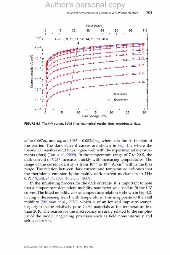
We theorectically simulated the dark current curves of THz QWP (ID:V267) (Tan et al., 2009). The bias range is from 0.1 to 30 mV, and the temper-atures are from 7 to 20 K. In the simulation, the saturated mobility is takenas υsat = 1× 107 cm/s; the energy of the ground state is E1 = 4.25 meV;the barrier height is Eb = 0.87x eV; and the effective mass of electron is
Author's personal copy
Semiconductors and Semimetals, Vol 84, 2011, pp. 195–242.
JAGADISH Ch04-9780123813374 2011/4/30 11:07 Page 205 #11
Terahertz Semiconductor Quantum Well Photodetectors 205
0
100
10−1
10−2
10−3
10−4
Cur
rent
den
sity
(A
/cm
2 )
10−5
10−6
10−7
16 32 48 64
Field (V/cm)
T = 7, 8, 9, 10, 11, 12, 14, 16, 18, 20 K
80 96 112
0 5 10 15Bias voltage (mV)
Simulation
Experiment
20 25 30
FIGURE 4.1 The I–V curves. Solid lines: mumerical results; dots: experimetal data.
m∗ = 0.067me and mb = (0.067+ 0.083x)me, where x is the Al fraction ofthe barrier. The dark current curves are shown in Fig. 4.1, where thetheoretical results (solid lines) agree well with the experimental measure-ments (dots) (Tan et al., 2009). In the temperature range of 7 to 20 K, thedark current of V267 increases quickly with increasing temperatures. Therange of the current density is from 10−5 to 10−1 A/cm2 within the biasrange. The relation between dark current and temperature indicates thatthe thermionic emission is the mainly dark current mechanism in THzQWP (Celik et al., 2008; Tan et al., 2009).
In the simulating process for the dark currents, it is important to notethat a temperature-dependent mobility parameter was used to fit the I–Vcurves. The fitted mobility versus temperature relation is shown in Fig. 4.2,having a decreasing trend with temperature. This is opposite to the Hallmobility (Stillman et al., 1970), which is of an ionized impurity scatter-ing origin in the relatively pure GaAs materials at the temperature lessthan 20 K. The reason for the discrepancy is surely related to the simplic-ity of the model, neglecting processes such as field nonuniformity andself-consistency.
Author's personal copy
Semiconductors and Semimetals, Vol 84, 2011, pp. 195–242.

JAGADISH Ch04-9780123813374 2011/4/30 11:07 Page 206 #12
206 J. C. Cao and H. C. Liu
106
105
104
103
102
6 9 12 15Temperature (K)
18 21
Mob
ility
(cm
2 /V
s)
FIGURE 4.2 Vertical electron drift mobilities in the device structure versus devicetemperatures (Tan et al., 2009).
3.3. Photocurrent
The distinct feature of photoconductive QWPs in contrast with the con-ventional intrinsic and extrinsic photoconductors is the discreteness, i.e.,incident photons are only absorbed in discrete quantum wells that arenormally much narrower than the inactive barrier regions. In this section,we discuss the photocurrent caused by intersubband excitations in a QWP.
The photocurrent spectrum is an important characteristic of the deviceperformance, which gives the peak response frequency and the sensitivityto the radiation. Compared with the wideband IR sources (such as Globar,Hg lamp, and so on), THz QWPs are narrowband detectors.
We calculated the spectral response of a THz QWP designed for 7 THzdetection peak frequency (Cao et al., 2006). We incorporate the effect ofGaAs optical phonons which give rise to a strong absorption in the regionof 34–36 meV and result in an increase in reflection because of the largerefractive change around this region. Comparing the calculated spectralshape with experiments, we show the improvement over the standardexpressions.
For QWPs, the total absorption coefficient η is usually defined asthe ratio of the absorbed electromagnetic energy per unit time, volume,and the intensity of the incident radiation. For simplicity, we define adimensionless absorption coefficient normalized by the area A instead of
Author's personal copy
Semiconductors and Semimetals, Vol 84, 2011, pp. 195–242.

JAGADISH Ch04-9780123813374 2011/4/30 11:07 Page 207 #13
Terahertz Semiconductor Quantum Well Photodetectors 207
the volume. The expression for η is given by
η =~ωIA
∑n,n′
∑k⊥
| < n|(e/m∗)A · P|n′ > |2
× [f (En(k⊥))− f (En′(k⊥))]× δ(En′(k⊥)− En(k⊥)− ~ω), (4.21)
where I is the intensity of the incident radiation and is given by
I = (1/2)ε0cn0E20. (4.22)
Here n0 is the refractive index of the material, taken to be real and constant,and E0 is the electric field amplitude (Liu and Capasso, 2000). ExpressingA by E0 and changing the summation into a two-dimensional integration(Liu and Capasso, 2000), we get
η =πe2
ε0cn0ωm∗2∑n,n′
2(2π)2
∫d2k⊥| < n|pz|n′ > |2
· [f (En)− f (En′)]δ(En − En′ − ~ω). (4.23)
The spectral current responsivity <i is given by
<i = Iphoto/(~ω8i), (4.24)
where 8i is the incident photon number per unit time. The photocurrentIphoto is given by
Iphoto = i(1)photo/pc, (4.25)
where
i(1)photo = e8iηpe/N (4.26)
is the photoemission current directly ejected from one well, N is the num-ber of quantum wells, pc is the capture probability, and pe is the escapeprobability for an excited electron from the well (Liu and Capasso, 2000).Using Eqs. (4.25) and (4.26), we get
<i =e
~ωηgphoto, (4.27)
where photoconductive gain is gphoto = pe/pcN.
Author's personal copy
Semiconductors and Semimetals, Vol 84, 2011, pp. 195–242.
JAGADISH Ch04-9780123813374 2011/4/30 11:07 Page 208 #14
208 J. C. Cao and H. C. Liu
Until now, we have assumed that the amount of absorption is the samefor all the wells and the absorption by the lattice is negligible (Ershov et al.,1999; Jovanovic et al., 2004). However, this assumption does not hold forthe present case. In the reststrahlen region (34–36 meV), the absorption bythe optical phonons of GaAs is very strong, and the amount of absorptionfor each well is not the same either. Therefore, 8i in Eq. (4.26) should bereplaced by 8(z), to take into account the difference between the incidentlight and the light propagating in the QWIP. For simplicity, we take theabsorption of the middle well as the average absorption, and use the lightintensity I instead of the photon number 8, I = ~ω8, then we have
<i =eηI(z)~ωIi
gphoto. (4.28)
Using the following standard expressions (Klingshirm, 1997), I(z) = I(z =0)e−2ωk(ω)z/c, I(z = 0) = (1/2)ε0cn(ω)E2
0 and Ii = (1/2)ε0cniE20, and Ii =
(1/2)ε0cniE20, where z is the distance from the middle well to the first well,
ni is the refractive index of air, and n(ω) is the refractive index of the matterin connection with Snells, law of refraction.
If we use a “single oscillator” model to simulate such absorption behav-ior in the reststrahlen region (Blakemore, 1982), we can easily get thecomplex refractive index
κ∗(ω) ≡ (κ1 − iκ2) = κ∞ +ω2
TO(κ0 − κ∞)
ω2TO − ω
2 + i2πγpω, (4.29)
where κ0 is the low–frequency dielectric constant, κ∞ is the high–frequency (optical) dielectric constant, ωTO is the resonant frequency, andγp is the damping coefficient. In addition, we have
n(ω) = (1/√
2)[(κ21 + κ
22 )
1/2+ κ1]1/2, (4.30)
k(ω) = (1/√
2)[(κ21 + κ
22 )
1/2− κ1]1/2. (4.31)
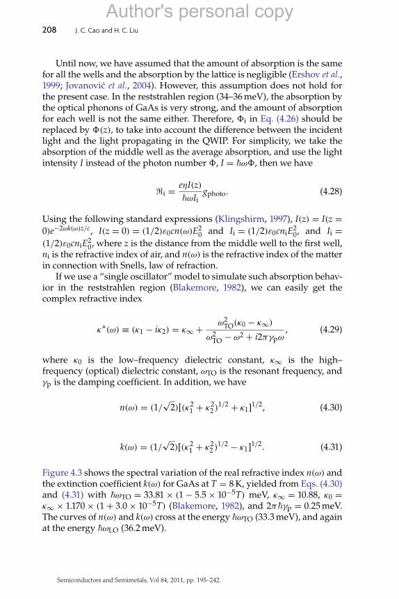
Figure 4.3 shows the spectral variation of the real refractive index n(ω) andthe extinction coefficient k(ω) for GaAs at T = 8 K, yielded from Eqs. (4.30)and (4.31) with ~ωTO = 33.81× (1− 5.5× 10⁻⁵T) meV, κ∞ = 10.88, κ0 =
κ∞ × 1.170× (1+ 3.0× 10⁻⁵T) (Blakemore, 1982), and 2π~γp = 0.25 meV.The curves of n(ω) and k(ω) cross at the energy ~ωTO (33.3 meV), and againat the energy ~ωLO (36.2 meV).
Author's personal copy
Semiconductors and Semimetals, Vol 84, 2011, pp. 195–242.

JAGADISH Ch04-9780123813374 2011/4/30 11:07 Page 209 #15
Terahertz Semiconductor Quantum Well Photodetectors 209
14
12
10
8
6
4
2
020 30 40 50
Photo energy (meV)
Rea
l ref
ract
ive
inde
x n
Ext
inct
ion
coef
ficie
nt k
60 70
GaAsT = 8K
n
k
80
FIGURE 4.3 Spectral variation of the real refractive index and the extinction coefficientfor GaAs at 8 K (Cao et al., 2006), modeled by Eqs. (4.30) and (4.31).
1.0
0.8
0.6
0.4
0.2
0.020 30 40
Abs
orpt
ion
effic
ienc
y η
50Photo energy (meV)
60 70
GaAs/AIGaAs QWIPT = 8K
TotalB–BB–C
80
FIGURE 4.4 Calculated absorption quantum efficiency versus photon energy for onewell with well width d = 12 nm and electron density 1017 cm−3 (Cao et al., 2006).
In the experiment of THz QWIP (Liu et al., 2004) discussing the rest-strahlen region, the device consists of 50 quantum wells made of 12-nmGaAs wells and 40-nm Al0.05Ga0.95As barriers. The center 10-nm regionof the wells was doped with Si to 1017 cm−3. The 45◦ edge facet geome-try was used for photoresponse measurement and the polarization is p.The applied voltage is only ±0.4 V and the voltage drop across a givenwell is less than 2 meV, which is negligible compared with the ground-state energy. The absorption spectrum is calculated at zero bias as anapproximation (Liu et al., 2004). First, the absorption coefficient is calcu-lated using Eq. (4.23) (Ikonic et al., 1989; Liu, 1993), as shown in Fig. 4.4.Here the ground state energy E0 = 14.2 meV, and the first excited stateenergy E1 = 43.1 meV is very close to the barrier height Vb. This optimum
Author's personal copy
Semiconductors and Semimetals, Vol 84, 2011, pp. 195–242.
JAGADISH Ch04-9780123813374 2011/4/30 11:07 Page 210 #16
210 J. C. Cao and H. C. Liu
design (Liu and Capasso, 2000) will bring both a large absorption and arapid escape for the excited electrons. From the results of the calculation,we can see that the peak detection wavelength (42.5 µm) is in good agree-ment with the design, and both bound-to-bound and bound-to-continuumintersubband transitions contribute to the absorption.
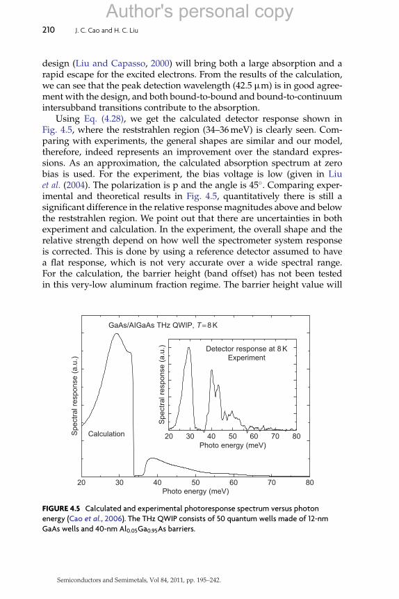
Using Eq. (4.28), we get the calculated detector response shown inFig. 4.5, where the reststrahlen region (34–36 meV) is clearly seen. Com-paring with experiments, the general shapes are similar and our model,therefore, indeed represents an improvement over the standard expres-sions. As an approximation, the calculated absorption spectrum at zerobias is used. For the experiment, the bias voltage is low (given in Liuet al. (2004). The polarization is p and the angle is 45◦. Comparing exper-imental and theoretical results in Fig. 4.5, quantitatively there is still asignificant difference in the relative response magnitudes above and belowthe reststrahlen region. We point out that there are uncertainties in bothexperiment and calculation. In the experiment, the overall shape and therelative strength depend on how well the spectrometer system responseis corrected. This is done by using a reference detector assumed to havea flat response, which is not very accurate over a wide spectral range.For the calculation, the barrier height (band offset) has not been testedin this very-low aluminum fraction regime. The barrier height value will
20
20
30 40 50Photo energy (meV)
Photo energy (meV)
Detector response at 8KExperiment
Calculation
GaAs/AIGaAs THz QWIP, T = 8K
Spe
ctra
l res
pons
e (a
.u.)
Spe
ctra
l res
pons
e (a
.u.)
60 70 80
30 40 50 60 70 80
FIGURE 4.5 Calculated and experimental photoresponse spectrum versus photonenergy (Cao et al., 2006). The THz QWIP consists of 50 quantum wells made of 12-nmGaAs wells and 40-nm Al0.05Ga0.95As barriers.
Author's personal copy
Semiconductors and Semimetals, Vol 84, 2011, pp. 195–242.
JAGADISH Ch04-9780123813374 2011/4/30 11:07 Page 211 #17
Terahertz Semiconductor Quantum Well Photodetectors 211
change the relative strength of contributions from bound-to-bound andbound-to-continuum transitions, and therefore change the overall shape.Moreover, many-body effects have not been included, which would havemoved the overall response to a higher energy and made a better fit inthe low-energy region (20–25 meV). In the experimental curve, there aresome smaller features, for example, dips at 42 and 45 meV. These may becaused by the weaker absorption of two-zone edge and AlAs-like phonons,and they may also be caused because of the absorption associated withthe localized vibrational modes of Si-doped GaAs. A lot of investiga-tions have been done on the absorption induced by Si-related defects indoped GaAs (Chen et al., 1980; Spitzer and Panish, 1969), and the frequen-cies of all the absorption bands of interest in their study is from 350 to480 cm−1 (43.4–59.6 meV). In addition, there may be absorption resultingfrom other localized phonon modes (Shen, 1984). We note that having anintersubband transition in resonance with optical photons may lead to astrong coupling and the formation of intersubband polarons. However,because the doping density in the device analyzed here is not high andthe intersubband oscillator strength is not large because of the bound-to-quasibound nature, the polaron splitting is expected to be about 1 meV orless (Liu et al., 2003). We, therefore, neglect the effect of strong coupling.
A more detailed comment is in order regarding the AlAs-like phonons.For alloys like AlGaAs, a more complex dielectric function should beused to describe a two-mode oscillator for GaAs-like and AlAs-like opticalphonons. However, if we take a simple model of either additive or factor-ized functions for the entire multiple quantum well stack, a very-strongabsorption would also result in the AlAs-like phonon region, which doesnot agree with experiment. This is an issue to be resolved, i.e., how toinclude the contribution of the AlAs-like phonon.
In conclusion, we have calculated and discussed the response spec-trum of a THz QWP. Because of the optical phonon absorption in thereststrahlen region, the refractive index n and the extinction coefficient kchange strongly. Considering all the changes, we have improved the usualexpression for <i, and obtained better agreement with experiments.
3.4. Many-body effects
Because of the low-doping density, the many-body effects are usuallyneglected in the design of midinfrared QWPs (Schneider and Liu, 2006).However, for THz QWPs, because the energy difference between thebound subband and the continuum is around 10 meV, notable error ofphotoresponse peak position will be introduced without considering themany-body effects (Liu et al., 2004; Schneider and Liu, 2006). The many-bodyeffects include the interactions among electrons and between electrons and
Author's personal copy
Semiconductors and Semimetals, Vol 84, 2011, pp. 195–242.

JAGADISH Ch04-9780123813374 2011/4/30 11:07 Page 212 #18
212 J. C. Cao and H. C. Liu
other quasiparticles. Earlier investigations have shown that in QWIPs, theelectron–electron interactions can affect the optical response peak position(Schneider and Liu, 2006). The other many-body interactions have influ-ence on the linewidth and line shape of photocurrent spectrum (Xionget al., 2008). We studied the many-body effects on THz QWPs (Guo et al.,2009). It is found that large differences between theory and experimentare introduced without including the above many-body interactions in thetheoretical design. Our numerical results show that it is very important toconsider the many-body interactions for designing THz QWPs.
In general, because of the large degrees of freedom of a many-particlesystem, many-body effects can only be treated with various approxi-mation methods. For electron–electron interactions, the static exchange-correlation and the dynamical depolarization (or local field) (Liu, 1994;Załuzny, 1993) and exciton-like effects are considered with local densityapproximation (LDA) within the framework of density functional the-ory. The depolarization and exciton-like interactions between the groundand excited sublevels are photon-induced many-body contributions (Funget al., 1999). For the electron–quasiparticle interactions, the electron–phonon and the electron-impurity scatterings are described by using asimple model with two free parameters (Fu et al., 2003; Xiong et al., 2008),the values of which are determined by fitting numerical photocurrentcurves to experimental data. Because of the low aluminum concentrationin barrier layers, the scattering between electron and interface roughnessis not considered.
The photocurrent spectra of two THz QWPs are calculated here; thedevice parameters are the two devices labeled as V266 and V267 reportedin the studies of Liu et al. (2004) and Luo et al. (2005). Our numerical resultsshow that there is only one bound subband in the quantum well with onlythe Hartree potential being considered. When the exchange-correlationpotential is taken into account, however, two bound subbands exist in thequantum wells for the two THz QWPs, and the second subband is nearthe top of the barrier. The static exchange-correlation and the dynamicaldepolarization electron–electron interactions cause blueshifts of the pho-toresponse peaks, and the calculated photocurrent peak positions agreewith the experimental data quantitatively. The shapes of the photocurrentpeaks are well described by the energy-dependent 0 model that representsthe effects of the electron–phonon and electron-impurity scatterings. TheLDA functional for exchange-correlation potential adopted in this chaptercannot properly describe the exciton-like many-body effect in THz QWPs.
The Hamiltonian for an electron in THz QWPs within the effective massapproximation is
H = p1
2m∗(z)p+ VQW(z)+ VH(z)+ Vxc(z), (4.32)
Author's personal copy
Semiconductors and Semimetals, Vol 84, 2011, pp. 195–242.

JAGADISH Ch04-9780123813374 2011/4/30 11:07 Page 213 #19
Terahertz Semiconductor Quantum Well Photodetectors 213
where m∗ is the electron effective mass, p is the momentum operator, VQWis the well confinement potential, VH is the Hartree potential, and Vxc isthe exchange-correlation potential. The wave function of electrons in theTHz QWPs is expressed as a two-dimensional plane wave times a one-dimensional envelope function along the growth direction, ψk,l
(r||, z
)=
exp(ir||·k||
)ϕkz,l (z), where r|| and k|| are the in-plane coordinate and
momentum, kz is the quasimomentum limited to the first Brillouin zoneassociated with the quantum well period, and l is the subband index. Withthe above approximation, the Schrodinger equation reads
[−
~2
2∂
∂z
(1
m∗(z)∂
∂z
)+ VQW(z)+ VH(z)+ Vxc(z)
]ϕl,kz(z) = εl,kzϕl,kz(z).
(4.33)
The energy of the electron is Ek,l = ~2k2||/2m∗ + εkz,l. The electron charge
density is given by
ρe (z) = |e|∑k,l
f(Ek,l, εF, T
) ∣∣ϕkz,l (z)∣∣2 , (4.34)
where e is the electron charge, f is Fermi distribution function, εF is theFermi energy, and T is temperature. Once the density is known, the Hartreepotential VH can be obtained by solving the Poisson equation
∂2
∂z2 VH (z) = −ρe (z)− ρd (z)
ε, (4.35)
where ρd (z) is the fixed ionized dopant density, and ε is dielectric con-stant. In general, it is a difficult task to find the exact exchange-correlationpotential Vxc. In this chapter, the widely used LDA based on the densityfunctional theory is adopted through the following formula (Gunnarssonand Lundqvist, 1976; Zhang and Potz, 1990):
Vxc(z) =e2
4π2εaBrs (z)
(94π
)1/3 [1+ 0.0545rs (z) ln
(1+
11.4rs (z)
)], (4.36)
where aB = ε~2/e2m∗ (z) is the effective Bohr radius and rs =[(3/4π)
(a3
Bρe(z))−1
]1/3. The band structure of THz QWP is obtained
by self-consistently solving the above set of equations with plane-waveexpansion method.
Author's personal copy
Semiconductors and Semimetals, Vol 84, 2011, pp. 195–242.

JAGADISH Ch04-9780123813374 2011/4/30 11:07 Page 214 #20
214 J. C. Cao and H. C. Liu
The absorption efficiency η can be derived from the Fermi’s golden rule
η (ω) =πe2
ε0cn0ωm∗2∑
j
∫dk(2π)3
∣∣⟨j ∣∣pz∣∣ 0⟩∣∣2
×[f(Ek,0, εF, T
)− f
(Ek,j, εF, T
)]δ(1Ek,l,0 − ~ω
), (4.37)
where ε0 is the vacuum permittivity, c is the speed of light, n0 is the refrac-tive index, and 1Ek,l,0 is the energy difference between the jth and theground subbands with depolarization and exciton-like effects included.The expression for 1Ek,l,0 is (Ando et al., 1982)
1E2k,l,0 = 1E2
k,l,0(1+ αk,l,0 − βk,l,0
),
αk,l,0 =2e2ρ2D
ε1Ek,l,0
∞∫−∞
dz
z∫−∞
dz′ϕkz,l(z′)ϕkz,0
(z′)2
,
βk,l,0 = −2ρ2D
1Ek,l,0
∞∫−∞
dzϕkz,l (z)2 ϕkz,0 (z)2∂Vxc [ρ (z)]∂ρ (z)
. (4.38)
Here αk,l,0 and βk,l,0 describe the depolarization and exciton-like effects,respectively, and 1Ek,l,0 is the energy difference between l and 0 subbandswithout the two dynamical many-body corrections. The photocurrent isIphoto = e8ηgphoto, where 8 is the incident photon number per unit time,and gphoto is the photoconductive gain. On the assumption of energy-independant 8 and gphoto, the photon current Iphoto is proportional to theabsorption efficiency η. For simplicity, the delta function in Eq. (4.37) isreplaced by a Lorentzian 0/
[π(Ek,j − Ek,0 − ~ω
)2+ 02
], where 0 is a small
constant. In Fu et al. (2003) and Xiong et al. (2008), an energy-dependent0 = a
√E− ~ωTO + b is used to take into account the effects of electron–
phonon and electron-impurity on the shape of photocurrent peak, wherea and b are parameters, and E is the electron energy measured fromthe conduction band edge of (Al,Ga)As barrier. In this chapter, the sameexpression of 0 is adopted to fit for the experimental results.
The band structures and photocurrents of two THz QWPs are calcu-lated. In order to compare with the experimental results, the parametersof the two THz QWPs, including the barrier and well widths, the bar-rier height, and the doping concentration and position, are those reportedin the studies of Liu et al. (2004) and Luo et al. (2005). The effective elec-tron mass is 0.067m0 with m0 the electron mass. The temperature is 8.0 K.To expand the envelope wave functions, 99 plane waves are used. The
Author's personal copy
Semiconductors and Semimetals, Vol 84, 2011, pp. 195–242.

JAGADISH Ch04-9780123813374 2011/4/30 11:07 Page 215 #21
Terahertz Semiconductor Quantum Well Photodetectors 215
0
(A) (B)
10
−10−0.04
−40 −20 0 20 40 −40 −20 0 20 40
−0.02 0.00 0.02 0.04
kz(1/nm)
z (nm)
−0.04 −0.02 0.00 0.02 0.04
20
Ene
rgy
(meV
) 30
40
50
FIGURE 4.6 Band structures of V266 THz QWP (A) without and (B) withexchange-correlations potential (Guo et al., 2009).
convergent criteria is∣∣(εFi − εFi−1)/εFi
∣∣ 5 0.0005, with εFi being the Fermienergy at the ith iterative step, and the convergence is reached in thecondition of i 5 15 for all the calculations.
Figure 4.6 shows the band structure of V266 THz QWP with and with-out the exchange-correlation potential. As shown in Fig. 4.6A, when theCoulomb interaction is taken into account with Hartree approximation,only one localized subband exists in the quantum well. The first excitedsubband is in resonance with the top of the barrier, which is in accordancewith the design rule of bound-to-quasibound QWIPs. However, becausethe quantum well is very shallow for THz QWPs, the neglect of exchange-correlation potential will introduce large errors in design of THz QWPs.Because the exchange-correlation potential is negative, for V266 THz QWP,the exchange-correlation interaction deepens the quantum well by about6.3 meV, which makes the first excited subband fall into the quantum welland be off resonance with the top of the barrier. The energy differencebetween the ground and the first excited subbands increases by about3.2 meV for V266 THz QWP. Similar effects of exchange-correlation interac-tion on the band structure of V267 THz QWP (not shown) are found. Theeffects of Hartree potential on the band structures of V266 and V267 arealso explored. Because the Si dopants are doped in well layers, the elec-trons and ionized dopants are spatially overlapped, which lowers theHartree contribution. The energy difference between the ground and the
Author's personal copy
Semiconductors and Semimetals, Vol 84, 2011, pp. 195–242.

JAGADISH Ch04-9780123813374 2011/4/30 11:07 Page 216 #22
216 J. C. Cao and H. C. Liu
first excited subbands increases by 0.4 meV for V266 and 0.3 meV for V267with Hartree potential being considered. The calculated results show thatthe exchange-correlation interaction plays a key role in the design of THzQWPs.
The theoretical and experimental photocurrent spectra for V266 andV267 are shown in Fig. 4.7. In order to obtain some physical insights, dif-ferent many-body interactions are taken into account step-by-step in ourcalculations. The energy differences of response peak positions betweentheory and experiment for V266 and V267 THz QWPs are 5.6meV (24.8%)and 4.8 meV (36.0%) without including any many-body interaction. Whenthe static exchange-correlation potentials are taken into account, the differ-ences decrease to 2.4 meV (10.6%) and 2.6 meV (19.4%), respectively. Thefurther improvements of theoretical response peak positions are achievedby considering the dynamical depolarization effects, and the discrepan-cies are about 0.2 meV (0.9%) and 1.1 meV (8.2%) for V266 and V267,respectively.
The exciton-like interaction plays a negative role in our calculations.Earlier investigations show that the value of βk,l,0 is much smaller than that
Nor
mal
ized
pho
tocu
rren
t
0.0
0.4
0.8
1.2
4 16 20 24
Exp. dataWithout Vxc
With Vxc
Vxc+ Depol.
288 12
100.0
0.4
0.8
1.2Exp. dataWithout Vxc
With Vxc
Vxc+ Depol.
Energy (meV)
(B)
(A)
15 20 25 30 35
FIGURE 4.7 Calculated and experimental photocurrent spectra of THz QWPs, (A) forV266 THz QWP and (B) for V267 THz QWP (Guo et al., 2009).
Author's personal copy
Semiconductors and Semimetals, Vol 84, 2011, pp. 195–242.
JAGADISH Ch04-9780123813374 2011/4/30 11:07 Page 217 #23
Terahertz Semiconductor Quantum Well Photodetectors 217
of αk,l,0 in Eq. (4.38) (Helm, 2000; Liu et al., 2007b). However, our numeri-cal results show that the value of βk,l,0 is in the same order of magnitudeas that of αk,l,0. The overestimate of exciton-like interaction in our workoriginates from the following two reasons: (1) in the current expressionfor Vxc in Eq. (4.36), ∂Vxc [ρ (z)] /∂ρ (z) is proportional to ρ (z)−2/3, whichwill lead to unreasonably large values of ∂Vxc [ρ (z)] /∂ρ (z) in barrier lay-ers. (2) because of the low barrier height, in comparison with midinfraredQWIPs, more portions of the wave function will extend into the barrierlayer. For the above two reasons, the integration value in Eq. (4.38) will beoverestimated. The value of βk,l,0 should be much smaller than that of αk,l,0(Schneider and Liu, 2006). Therefore, for the present work, we leave outthe exciton-like contribution.
In conclusion, we have investigated the effects of exchange-correlation,depolarization, and exciton-like interactions on the photon response spec-tra of THz QWPs. Because of the decrease of energy difference betweenthe ground subband and the first excited subband, large relative errors areintroduced without including the above many-body interactions in the the-oretical design. The exchange-correlation potential deepens the quantumwell. As a result, the ground subband and the first excited subband shift tothe lower energy region, and the energy difference between them increases.Because the expression for exchange-correlation potential is inadequate inthe low electron density region and the leakage of wave function into thebarrier layer, the exciton-like interaction is overestimated. The discrepancybetween the theoretical and experimental photoresponse peak positionsdecreases evidently by including the exchange-correlation and depolariza-tion effects. Our numerical results show that it is very important to considerthe many-body interactions for designing THz QWPs.
3.5. Simulation and optimization of grating coupler
The ISBT selection rule requires a nonzero polarization component in thequantum well direction (the epitaxial growth direction, z) (Schneider andLiu, 2006). As mentioned earlier, 45◦ incident, light-coupling geometryis usually used to acquire a nonzero polarization in z direction. How-ever, this prevents the construction of two-dimensional (2D) focal planearrays, which need light incident normal to the devices (the QW planes,xy plane). To solve this problem, it is useful to utilize gratings, as exploitedby Heitmann et al. (1982) to diffract the light and thus excite ISBT in Siinversion layers. In the midinfrared region, large-format arrays with up to1024× 1024 pixels have already been demonstrated (Gunapala et al., 2005).Recently, Patrashin et al. (2006) fabricated one-dimensional (1D) metal grat-ings on the top of the THz QWP, realizing device response under normalincidence (Patrashin and Hosako, 2008).
Author's personal copy
Semiconductors and Semimetals, Vol 84, 2011, pp. 195–242.

JAGADISH Ch04-9780123813374 2011/4/30 11:07 Page 218 #24
218 J. C. Cao and H. C. Liu
We utilized Modal method (Todorov and Minot, 2007) to simulate thefield distribution in the 1D metal grating THz QWP (Zhang et al., 2011). Theaverage intensity in device active region was obtained. Based on numericalresults, the optimizations of the grating including period and fill factor werediscussed, which led to high coupling efficiency and device responsivity.
Usually, GaAs/AlGaAs material system is used to fabricate THz QWPs.The device is grown on semi-insulating (SI) GaAs substrate. From the bot-tom to the top, there are bottom contact, multiple quantum wells and topcontact, shown in Fig. 4.8. The top and bottom contacts are n-doped GaAs,and the multiple quantum wells consist of several tens of AlGaAs bar-rier and n-doped GaAs well. The 1D metal grating is made of gold andis defined using standard mirofabrication lift-off techniques. The periodof the grating is d, and the width of metal stripe is a.
The modal method is proposed by Todorov and Minot (2007). Thismethod combines the Rayleigh expansion method of the diffracted fieldand the transfer matrix method of the multilayer, by which the electricfield distribution in the device can be obtained conveniently.
The field appears in the form of a Rayleigh expansion in the homoge-neous layers outside the 1D grating:
ψ(x, y, z
)= eiβy
∞∑n=−∞
eiαnx(
Pneiγnz+Qne−iγnz
), (4.39)
Top contact
THz waves 1D metal gratingx
z
AIGaAs
AIGaAsGaAs
Mul
tilay
er
AIGaAs
Bottom contact
SI GaAs substrate T
QP
0th diffractive mode
1st diffractive mode
GaAs
FIGURE 4.8 Schematic of 1D grating THz QWP (Zhang et al., 2011).
Author's personal copy
Semiconductors and Semimetals, Vol 84, 2011, pp. 195–242.

JAGADISH Ch04-9780123813374 2011/4/30 11:07 Page 219 #25
Terahertz Semiconductor Quantum Well Photodetectors 219
αn = α +2πn
d, (4.40)
γn =
√εk2
0 − α2n − β
2, (4.41)
where ψ is any component of the field, ε is the dielectric function of thematerial, k0 is the wave vector in the vacuum, and αn is the wave vector in xdirection. The x, y, and z direction are shown in Fig. 4.8. α0 = α is the wavevector of incident wave in x direction. The conservation of the tangentialcomponent of the wave vector at the grating surface leads to Eq. (4.40). βand γn are the wave vectors in y and z direction, respectively. (Pn,Qn) isthe pair of amplitudes (see Fig. 4.8), and all the pairs in different layersare connected with each other through transfer matrix. For the incidentarea outside the device, Qn = 0 except Q0, and Q0 = 1 if the amplitude ofincoming wave is set to be 1; while for the transmitted area, Pn = 0 andQn = Tn.
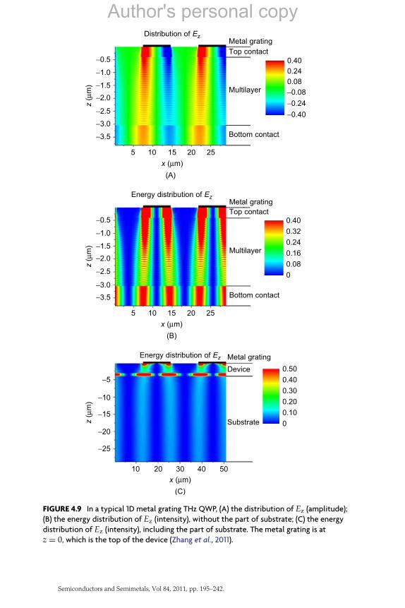
The field distribution can be obtained by solving the simultaneousequations in different areas with the boundary conditions. For normalincidence, only p polarization is need to be considered because no con-tribution is from s polarization which is in parallel with the QW planesmakes no contribution. A typical field distribution (Ez component) in 1Dmetal grating THz QWP is shown in Fig. 4.9 (only Ez component con-tributes to the ISBT). Compared with the total thickness of the active region(less than 5 µm), the GaAs substrate is much thicker, normally around600 µm, which is also much longer than the wavelength. So an approxi-mation of infinite substrate is taken in the calculation for simplicity, whichwill not affect the diffractive characteristic of the grating.
In Fig. 4.9A and B, we can see a pair of stripes beneath the grating. Thisindicates the diffraction occurs and the nonzero Ez component appears,which will cause the response of the detector. The field distribution in thesubstrate is also given in Fig. 4.9. The periodic dark and light stripes aresimilar with the multislit interference. In the following, we will discussthe optimization of the 1D metal grating based on the Ez in the activeregion.
Two THz QWPs are considered here (Liu et al., 2008). The multilayeris sandwiched between 0.4 and 0.8 µm of top and bottom contacts, dopedto 1.0× 10¹⁷. The structures are detailed in Table 4.1. The optimization isdiscussed from the period d and the fill factor r (i.e., the ratio of metal stripewidth a and d).
Lw is the quantum well width, Lb is the barrier width, N is the periodnumber of multilayer, [Al] is the Al fraction in the barrier, Nd is the dopingdensity in the well, and f0 is the peak response frequency of the device.
Author's personal copy
Semiconductors and Semimetals, Vol 84, 2011, pp. 195–242.
JAGADISH Ch04-9780123813374 2011/4/30 11:07 Page 220 #26
5
−3.5
−3.0
−2.5
−2.0
−1.5
−1.0
−0.5
10 15 20 25
(A)
(B)
(C)
Bottom contact
Multilayer
Top contact0.400.240.08
−0.08
−0.24
−0.40
Metal gratingDistribution of Ez
x (µm)
z (µ
m)
Bottom contact
5
−3.5
−3.0
−2.5
−2.0
−1.5
−1.0
−0.5
10 15 20
x (µm)
z (µ
m)
25
Multilayer
Top contact0.40
0.32
0.24
0.16
0.08
0
Metal gratingEnergy distribution of Ez
Device
Substrate
10
−25
−20
−15
−10
−5
20 30 40 50
x (µm)
z (µ
m)
0.50
0.40
0.30
0.20
0.10
0
Metal gratingEnergy distribution of Ez
FIGURE 4.9 In a typical 1D metal grating THz QWP, (A) the distribution of Ez (amplitude);(B) the energy distribution of Ez (intensity), without the part of substrate; (C) the energydistribution of Ez (intensity), including the part of substrate. The metal grating is atz = 0, which is the top of the device (Zhang et al., 2011).
Author's personal copy
Semiconductors and Semimetals, Vol 84, 2011, pp. 195–242.
JAGADISH Ch04-9780123813374 2011/4/30 11:07 Page 221 #27
Terahertz Semiconductor Quantum Well Photodetectors 221
TABLE 4.1 The structure parameters of THz QWPs
LW (A) Lb (A) N [Al] Nd (cm−3) f 0 (THz)
A 155 702 30 3% 6× 10¹⁶ 5.41B 221 951 23 1.5% 3× 10¹⁶ 3.21
The dielectric function is taken as follows (Blakemore, 1982):
ε(ω) =ω2
TO (εs − ε∞)
ω2TO − ω
2 − iωδTO+ ε∞
[1−
ω2P
ω (ω + iδP)
](4.42)
For GaAs, εs = 12.85, ε∞ = 10.88, ωTO = 2π × 8.02 THz, δTO = 2π ×0.06 THz, δP is the damping rate, depending on the doping density NP,Drude frequency ωP is
ωP =
√NPe2
ε0εsm∗, (4.43)
where e is the charge of electron, and m∗ is the effective mass of freecarriers.
The Drude model of metal is
εM (ω) = 1−ω2
Mω (ω + iδM)
(4.44)
For gold, ωM = 1.11× 10⁴ THz and δM = 83.3 ps−1.The thickness of 1D metal grating studied here is 0.38 µm, deposited
on the top of top contact. With these parameters, we calculate the averageintensity Iaverage of Ez in the active region at the peak response frequencyf0, which are 5.41 THz and 3.21 THz for device A and B, respectively. Theexpression of Iaverage is
Iaverage = C
∫ ∣∣Ezeiωt∣∣2dV
V(4.45)
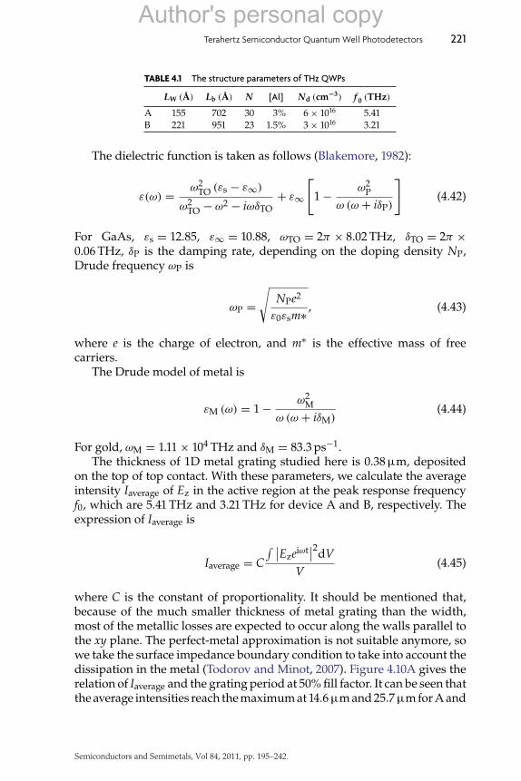
where C is the constant of proportionality. It should be mentioned that,because of the much smaller thickness of metal grating than the width,most of the metallic losses are expected to occur along the walls parallel tothe xy plane. The perfect-metal approximation is not suitable anymore, sowe take the surface impedance boundary condition to take into account thedissipation in the metal (Todorov and Minot, 2007). Figure 4.10A gives therelation of Iaverage and the grating period at 50% fill factor. It can be seen thatthe average intensities reach the maximum at 14.6 µm and 25.7 µm for A and
Author's personal copy
Semiconductors and Semimetals, Vol 84, 2011, pp. 195–242.
JAGADISH Ch04-9780123813374 2011/4/30 11:07 Page 222 #28
222 J. C. Cao and H. C. Liu
(B)
0.0
0.00
0.04I ave
rage
(a.u
.)
0.08
0.12
0.16
0.2 0.4 0.6Filling factor a/d
0.8 1.0
(A)
0
0.00
0.04
0.08
0.12
0.16
5 10 15 20 25d (µm)
30 35 45
I ave
rage
(a.
u.)
40
Device ADevice B
Device ADevice B
FIGURE 4.10 At peak response frequency (A) Iaverage versus the grating period under thecondition of 50% fill factor; (B) Iaverage versus the fill factor when the period of grating isset to match the wavelength (Zhang et al., 2011).
B, respectively, which correspond to the wavelength of THz waves at f0 in thedevice material (in GaAs, 5.41 THz corresponds to 14.6 µm, and 3.21 THzcorresponds to 25.7 µm). Therefore, when the period of the grating equalsthe wavelength in the device material, the coupling efficiency reaches themaximum. Then, we fix the grating period according to the peak response,and study the relation between average intensity and the fill factor. Theresults are given in Fig. 4.10B. For device A, the maximum occurs at 54.5%when the grating period is 14.6 µm; and for device B, it is 61.5% when thegrating period is 25.7 µm. The results are not 50%, which may be related tothe transmission and reflection of the multilayer. So the fill factor shouldbe determined according to the specific structure of a THz QWP.
To confirm these predictions, we fabricated three grating samples(A-G12 with a 12-µm-period grating, A-G15 with a 15-µm-period grat-ing, and A-G20 with a 20-µm-period grating). At 0.15-V bias, the peakresponsivities are 0.128, 0.197, and 0.070 A/W for A-G12, A-G15, and A-G20, respectively. It can be seen that, the 15-µm-period grating is the mostefficient one, which is in consistent with our prediction.
In conclusion, the Modal method is used to analyze the electric fielddistribution in the 1D metal grating THz QWP, and the optimization of thegrating is also discussed based on the simulation. We find that, when theperiod of the grating equals the wavelength in the material and a properfill factor is chosen (54.5% for A device, 61.5% for B device), the couplingefficiency reaches a maximum, leading to high field intensity and highdetector’s responsivity. Moreover, we find that the thickness of substrateis important for the field distribution, which may be caused by the cavityeffect. Further investigation is needed.
Author's personal copy
Semiconductors and Semimetals, Vol 84, 2011, pp. 195–242.

JAGADISH Ch04-9780123813374 2011/4/30 11:07 Page 223 #29
Terahertz Semiconductor Quantum Well Photodetectors 223
4. DESIGN AND CHARACTERIZATION OF THz QWP
4.1. Design
The detection of THz waves is the one of the key technology of THz applica-tions. To study the THz wave itself and its interaction with other materials,various characterizations should be done, including spectrum measure-ment, power calibration, beam analysis, and so on. Because of the specificposition in the electromagnetic wave spectrum, the study of THz rangedeveloped slowly for a long time because of the lack of radiation sourcesand detectors, and hence limited the methods that could be used for detec-tion. In the recent 10 years, as the development of compact THz sources andthe detection methods, the methods for detection of THz waves improvedsubstantially (Tonouchi, 2007). Therefore, different sources and detectorscould be chosen, and various physical phenomena could be studied.
THz QWP is the extension of QWIP in THz range. The materials arecommonly GaAs/AlGaAs. The optimum QW parameter for a standardQWIP is to have the first excited state in resonance with the top of the bar-rier. Strong ISBT absorption and fast relaxation of excited electrons can beboth achieved in this structure. Therefore, the structure parameters shouldbe optimized in design. These strcture parameters are the quantum wellwidth, barrier width, doping density, barrier height (the Al fraction inAlGaAs barrier), and the number of quantum wells. For THz QWP work-ing at longer wavelength than QWIP, smaller barrier height and lowerdoping density are required (to reduce the absorption by free carriers andthe dark current).
In 2004, Liu et al. (2004) demonstrated the first THz QWP with a peakresponse at 7.1 THz (42 µm). The width of quantum well and barrier are12 nm and 40 nm, respectively. The Al fraction is 5%, and the number ofquantum wells is 50. The center 10 nm of the quantum well and the top(400 nm) and bottom (700 nm) GaAs contacts are doped to 1017 cm−3 by Si.
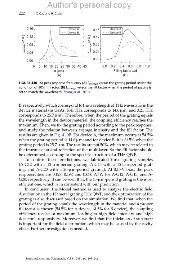
The calculated parameters of barrier Al percentage and well widthfor a given peak detection frequency (wavelength) are shown in Fig. 4.11(Liu et al., 2004). A word of caution: the parameters used here, althoughexpected to be valid, are proven for midinfrared QWIPs and are not testedin the low aluminum fraction region. From Fig. 4.11, it is predicted that theTHz frequency range of 1–8 THz is covered by QWIPs with low aluminumfractions between 0.8 and 5.4%.
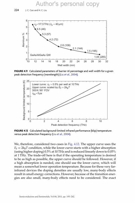
Figure 4.12 shows the calculated Tblip versus the peak detection fre-quency (Liu et al., 2004). For achieving the highest dark-current-limiteddetectivity, if one follows the Ef = 2kBT rule, the density would becomevery low for low temperatures (�80 K), making the absorption also low.
Author's personal copy
Semiconductors and Semimetals, Vol 84, 2011, pp. 195–242.
JAGADISH Ch04-9780123813374 2011/4/30 11:07 Page 224 #30
224 J. C. Cao and H. C. Liu
100
1
2
3
4
56.5 (46)
5.3 (57)
4.2 (72)
2.8 (108)2.1 (144)
1.5 (195)
1.05 (285)
6
12 14 16 18 20 22 24 26
Well width (nm)
GaAs/AlGaAs QW
νp= f /7.5THz (λp = 40 µm)A
lum
inum
%
28 30 32
FIGURE 4.11 Calculated parameters of barrier Al percentage and well width for a givenpeak detection frequency (wavelength) (Liu et al., 2004).
00
5
10
15
20
25
2 4 6 8
Peak detection frequency (THz)
Lower curve: η1 = 0.5% per well at 10THzUpper curve: scaled by EF = 2kBT300K / 90° FOVτlife= 5 ps
Bac
kgro
und
limite
d te
mpe
ratu
re (
K)
10
FIGURE 4.12 Calculated background-limited infrared performance (blip) temperatureversus peak detection frequency (Liu et al., 2004).
We, therefore, considered two cases in Fig. 4.12. The upper curve uses theEf = 2kBT condition, while the lower curve starts with a higher absorption(using higher doping) 0.5% at 10 THz and is reduced linearly down to 0.05%at 1 THz. The trade-off here is that if the operating temperature is desiredto be as high as possible, the upper curve should be followed. However, ifa high absorption is needed, one should use the lower curve, which willmean a somewhat lower operation temperature. Because for these very far-infrared devices the doping densities are usually low, many-body effectsresult in small energy corrections. However, because of the transition ener-gies are also small, many-body effects need to be considered. The exact
Author's personal copy
Semiconductors and Semimetals, Vol 84, 2011, pp. 195–242.
JAGADISH Ch04-9780123813374 2011/4/30 11:07 Page 225 #31
Terahertz Semiconductor Quantum Well Photodetectors 225
values depend on doping densities. The detection frequency in Fig. 4.12should, therefore, be shifted to higher values by about 30% if these effectsare included. In general, to qualify as a good detector, there must be asufficiently high absorption. On one hand, a high doping is desirable forachieving high absorption; but on the other hand, high doping leads to ahigh dark current and low operating temperature. A trade-off must, there-fore, be made for a given application. For most applications, it is desirableto operate the detector under the blip condition for detecting weak signals.In some applications involving a strong source such as a THz QCL, therequirement is different. Here as long as the dark current is lower than thesignal photocurrent, photon noise limited detection is achieved. In such acase, the detector operating temperature can be raised.
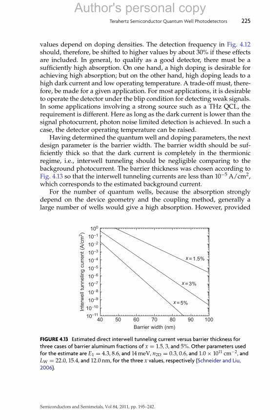
Having determined the quantum well and doping parameters, the nextdesign parameter is the barrier width. The barrier width should be suf-ficiently thick so that the dark current is completely in the thermionicregime, i.e., interwell tunneling should be negligible comparing to thebackground photocurrent. The barrier thickness was chosen according toFig. 4.13 so that the interwell tunneling currents are less than 10−5 A/cm2,which corresponds to the estimated background current.
For the number of quantum wells, because the absorption stronglydepend on the device geometry and the coupling method, generally alarge number of wells would give a high absorption. However, provided
100
10−1
10−2
Inte
rwel
l tun
nelin
g cu
rren
t (A
/cm
2 )
10−3
10−4
10−5
10−6
10−7
10−8
10−9
40 50 60 70
Barrier width (nm)
80
x=5%
x=3%
x=1.5%
90 100
10−10
10−11
FIGURE 4.13 Estimated direct interwell tunneling current versus barrier thickness forthree cases of barrier aluminum fractions of x = 1.5, 3, and 5%. Other parameters usedfor the estimate are E1 = 4.3, 8.6, and 14 meV, n2D = 0.3, 0.6, and 1.0× 1011 cm−2, andLW = 22.0, 15.4, and 12.0 nm, for the three x values, respectively (Schneider and Liu,2006).
Author's personal copy
Semiconductors and Semimetals, Vol 84, 2011, pp. 195–242.
JAGADISH Ch04-9780123813374 2011/4/30 11:07 Page 226 #32
226 J. C. Cao and H. C. Liu
0.080.07(A)
(B)
0.060.050.040.03
GaAs substratetransmission
Detector responseat 8K
Wavelength (µm)
0.02
0.080.070.060.05Photon energy (eV)
0.040.030.02
50
40
30
20
10
0
80 70 60 50 40 30 20
Spe
ctra
l res
pons
e (a
.u.)
Tra
nsm
issi
on (
%)
FIGURE 4.14 (A) Photoresponse spectrum and (B) low temperature bulk GaAstransmission spectrum (Liu et al., 2004).
a sufficient absorption is reached, a small number of wells is preferred forhigh gain.
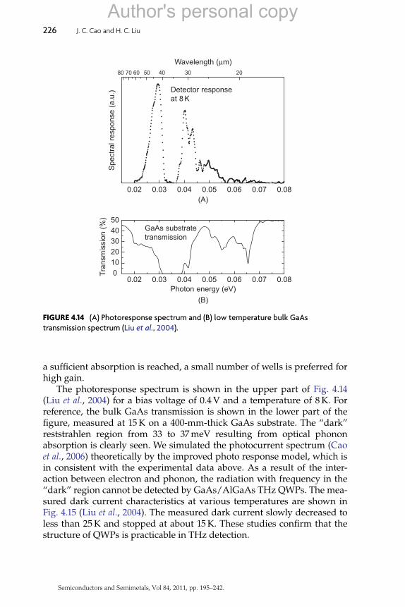
The photoresponse spectrum is shown in the upper part of Fig. 4.14(Liu et al., 2004) for a bias voltage of 0.4 V and a temperature of 8 K. Forreference, the bulk GaAs transmission is shown in the lower part of thefigure, measured at 15 K on a 400-mm-thick GaAs substrate. The “dark”reststrahlen region from 33 to 37 meV resulting from optical phononabsorption is clearly seen. We simulated the photocurrent spectrum (Caoet al., 2006) theoretically by the improved photo response model, which isin consistent with the experimental data above. As a result of the inter-action between electron and phonon, the radiation with frequency in the“dark” region cannot be detected by GaAs/AlGaAs THz QWPs. The mea-sured dark current characteristics at various temperatures are shown inFig. 4.15 (Liu et al., 2004). The measured dark current slowly decreased toless than 25 K and stopped at about 15 K. These studies confirm that thestructure of QWPs is practicable in THz detection.
Author's personal copy
Semiconductors and Semimetals, Vol 84, 2011, pp. 195–242.

JAGADISH Ch04-9780123813374 2011/4/30 11:07 Page 227 #33
Terahertz Semiconductor Quantum Well Photodetectors 227
10−1
100
101
10−2C
urre
nt (
A/c
m2 )
10−3
10−4
10−5
−1.5 −1.0 −0.5 0.0
15, 20, 25, 30, 35 KSymbols: measuredLines: model
Field (kV/cm)0.5 1.0 1.5
FIGURE 4.15 Dark current characteristics at various temperatures (Liu et al., 2004).
In addition, Graf et al. (2004) demonstrated a THz quantum wellphotodetector based on the quantum cascade structure, with the peakresponse wavelength of 84 µm (3.57 THz), operating at 10–50 K. Theresponsivity at 10 K is 8.6 mA/w. Although the detectivity and the respon-sivity are two orders of magnitude smaller than the THz QWP based onphotoemission, its noise level is relative low because of the cascade mech-anism. Because of the potential of zero bias photovoltaic response, thedevelopment of this type of detectors is also very interesting.
4.2. Measurement of photocurrent spectrum
Terahertz radiation bridges the gap between the microwave and opticalregimes. It is only 5 years since the first demonstration of THz QWP (Liuet al., 2004), and a lot of researches are still needed. Before the measurementof photocurrent spectrum, we test the I–V curves first, then analyze thedark current mechanism and the temperature performance.
The temperature-dependent I–V properties are important characteris-tics for terahertz QWPs. In the following, we measured the I–V curves with300 K background or the dark condition, and the relation between darkcurrent and temperature is also discussed. The active region of the deviceis GaAs/AlGaAs multiquantum wells grown by MBE. The parameters ofthe active region are shown in Table 4.2. It should be mentioned that thedoping in Table 4.2 is implemented at the center 10 nm of the quantumwell by Si. The purpose of the wide barriers is to reduce the interwell tun-neling (Liu et al., 2007a). In a real device, the active region is between thetop and bottom contacts. The top and bottom contacts are usually 400 and800 nm respectively, doped to 1× 1017 cm−3 with Si, which is relatively low
Author's personal copy
Semiconductors and Semimetals, Vol 84, 2011, pp. 195–242.
JAGADISH Ch04-9780123813374 2011/4/30 11:07 Page 228 #34
228 J. C. Cao and H. C. Liu
TABLE 4.2 Structure parameters for the THz QWIPs(Schneider and Liu, 2006)
Sample Lw (nm) Lb (nm) [Al] Nd (cm−3) NV265 11.9 55.2 0.05 1× 10¹⁷ 40V267 22.1 95.1 0.015 3× 10¹⁶ 23
to reduce the contact layer free carrier absorption and plasma reflection inthe THz region (Schneider and Liu, 2006). Next, we will mainly introducethe measurement and analysis of V267.
Mesa devices of different sizes were fabricated using standard GaAsprocessing techniques. Because low temperatures are required for opera-tion, a close-cycle cryostat with the lowest temperature of 3 K is used tocool the device. A source meter is used to provide the external bias, andthe current is also recorded at the same time. The bias range is from 1 to30 mV during the measurement.
The current–voltage curves under dark condition (solid) and under a90◦ FOV 300-K background (dash) at the temperatures from 3.15 to 20 K areshown in Fig. 4.16. Because thermionic emission and field-assisted tunnelingwere much stronger than interwell tunneling within the experiment temper-ature range, we did not observe any current bottom-out behavior (Schneiderand Liu, 2006). As in Section 2. Tblip is a good figure-of-merit of a detector.The measured Tblip of V267 is 12 K. Sequential tunneling and thermionicemission are two major dark current mechanisms in GaAs/AlGaAs bar-rier structures (Levine, 1993), and the latter becomes dominant for thickbarrier structures. From the I–V curves in Fig. 4.16A, the I–T curves havebeen obtained and shown in Fig. 4.16B. The dark current decreased by sixto seven orders of magnitude in accordance with the thermally activatedcharacter of the thermionic emission (Celik et al., 2008) when the devicewas cooled from 20 K down to 3.15 K, which indicates that the use of theemission-capture model, combined with the 3D carrier drift model, is rea-sonable for describing the dark current of this detector. A steep drop of theI–T curves when the device temperature≤12 K has been observed, which isconsistent with the good performance when the device is operating at andlower than Tblip. Next, we will introduce the measurement and analysisthe photocurrent spectra of 2 THz QWPs (V265 and V267).
The measured photocurrent spectra of V267 at different bias voltages aregiven in Fig. 4.17A. The operating temperature is 3.15 K. The peak responseis 3.2 THz, corresponding to 93.6-µm wavelength. Strong response alsoexists in the range from 3 to 5.3 THz, which can be used to characterize theTHz radiation source in this region. In addition, the photocurrent spectra atdifferent operating temperatures under 30-mV bias are also measured, seeFig. 4.17B. Upon increasing of the operating temperature, the photocurrent
Author's personal copy
Semiconductors and Semimetals, Vol 84, 2011, pp. 195–242.

JAGADISH Ch04-9780123813374 2011/4/30 11:07 Page 229 #35
Terahertz Semiconductor Quantum Well Photodetectors 229
(A)
(B)
100
101−100 −50 0
T = 3.15, 4.2, 6.0, 8.0, 10, 12, 16, 20KDark
Background
50
Field (V/cm)
Bias voltage (mV)
100
−30 −20 −10 0 10 20 30
10−1
10−2
10−3
10−4
10−5Cur
rent
den
sity
(A
/cm
2 )
10−6
10−7
100
10−1
10−2
10−3
10−4
Cur
rent
den
sity
(A
/cm
2 )
10−5
10−6
10−7
10−84 8 12
Temperature (K)16 20
30 mV
20 mV
10 mV
5mV
1mV
FIGURE 4.16 (A) Current–voltage curves of V267 under dark condition (solid)and under a 90◦ FOV 300-K background (dash) at different temperatures; (B)Current–temperature characteristic measured at selected bias voltages.
Author's personal copy
Semiconductors and Semimetals, Vol 84, 2011, pp. 195–242.

JAGADISH Ch04-9780123813374 2011/4/30 11:07 Page 230 #36
230 J. C. Cao and H. C. Liu
Wavelength (µm)
120
1.0
0.8
0.6
Pho
tocu
rren
t (a
rb. un
its)
0.4
0.2
0.0
1.0
0.8
0.6
Pho
tocu
rren
t (a
rb. un
its)
0.4
0.2
0.0
80 40
V267 @ 3.15 K
3.15K4.2K5.0K
2 4 6 8
Frequency (THz)
10 12 14
V267 @ 30mV
32mV30mV25mV20mV15mV10mV8mV
(A)
(B)
FIGURE 4.17 Photocurrent spectra of V267 at (A) different bias voltages and(B) different operating temperatures.
response decreases. The shape of the spectra doesn’t change significantlybecause of the small temperature range of the measurement.
Photocurrent spectra of V265 at different bias voltages at 3.5 K areshown in Fig. 4.18. It can be seen that the peak response is 9.7 THz (wave-length of 31.0 µm). The theoretical peak response is around 7 THz for thestructure of V265. The differences are caused by the phonon absorptionof GaAs, leading to a dark region from 32 to 37 meV. Stronger photocur-rent could be generated with higher bias, so the amplitude of photocurrentspectrum increases when the external bias is increased.
Author's personal copy
Semiconductors and Semimetals, Vol 84, 2011, pp. 195–242.

JAGADISH Ch04-9780123813374 2011/4/30 11:07 Page 231 #37
Terahertz Semiconductor Quantum Well Photodetectors 231
Wavelength (µm)120
1.0 600mV
400mV
200mV
100mV
50mV
1.2
0.8
0.6
Pho
tocu
rren
t (a
rb. un
its)
0.4
0.2
0.0
2 4 6 8Frequency (THz)
10 12 14
80 40
V265 @ 3.5 K
FIGURE 4.18 Photocurrent spectra of V265 at different bias voltages at 3.5 K.
4.3. THz QCL emission spectrum measured by THz QWP
We use a THz QWP to characterize the emission spectrum of a THzQCL (Tan et al., 2010). The shape and peak of the emission spectrum areacquired, and the relation of the emission power with driving current isestimated, from which the current density range of lasing and the thresh-old are obtained. The detection performance of THz waves from the THzQCL by THz QWP is also studied at different temperatures. We found thatTHz QWP is a good detector in characterizing the emission spectrum ofTHz QCL. The emission spectrum is an important characterization of alaser. Usually to measure the emission spectrum of a THz QCL, a FourierTransform Spectrometer is used. To reduce the absorption by the watervapor, the spectrometer should be evacuated. A bolometer operating atthe liquid helium temperature is often used to measure weak signal. Inthis section, we will mainly introduce the measurement of the emissionspectrum of a continuously THz QCL by a Fourier Transform Far-InfraredSpectrometer operating at linear scan mode.
The structure of the active region of the THz QCL is given in the study byLi et al. (2009b), and the sample ID is B1316 PKG3. Because low temperatureis required for the laser operation, we use a close-cycle cryostat to cool thelaser. The lowest temperature is 9 K. The radiation of the THz QCL enters theFTIR through the windows of the cryostat and the spectrometer. The scan
Author's personal copy
Semiconductors and Semimetals, Vol 84, 2011, pp. 195–242.

JAGADISH Ch04-9780123813374 2011/4/30 11:07 Page 232 #38
232 J. C. Cao and H. C. Liu
speed and the resolution of the FTIR are set to be 1.6 KHz and 0.25 cm−1,respectively. The beam splitter is 6 µm Mylar, and the detector is DTGS-PE.The range of wave number is 100–160 cm−1, and the THz QCL is driven bya DC bias at 10 K. We measured the emission spectra of the THz QCL atdifferent driving currents and operation temperatures.
THz QCL and THz QWP are both multiquantum well devices. Hosakoet al. (2007) suggested that THz QWP could be used to detect the emissionof THz QCL. In the following, we will use a THz QWP to characterize theemission spectrum of a THz QCL.
Before the characterization of THz QCL using THz QWP, we discussthe feasibility from the spectra (Tan et al., 2010). The photocurrent spec-trum of the THz QWP at 3.15 K under the illumination of a Globar isshown in Fig. 4.19. In order to compare with the emission spectrum ofthe THz QCL, the photocurrent signal is normalized, the inset shows thesame spectra on an expanded range. It can be seen that the responsepeak of the THz QWP is 3.2 THz. The response at 4.13 THz is about67% of the peak, and strong response occurs in the range of 3–5.3 THz
Wavenumber (cm−1)110
1.2
1.0
0.8
0.6
0.4
0.2
0.0
3.2 3.4
4 8 120.0
0.5
1.0
Nor
mal
ized
sig
nal (
arb.
uni
ts)
3.6 3.8
Frequency (THz)
Frequency (THz)
4.0 4.2 4.4
THzQWP (3.15K)
THzQCL (0.342A)
THzQCL (0.412A)
THzQCL (0.372A)
THzQWP (3.15K)
THzQCL (0.342A)
Nor
mal
ized
sig
nal (
arb.
uni
ts)
THzQCL (0.412A)
THzQCL (0.372A)
115 120 125 130 135 140 145
FIGURE 4.19 Comparison of the photocurrent spectrum of the THz QWP and theemission spectrum of the THz QCL. The operation temperatures are 3.15 and 10 K for THzQWP and THz QCL, respectively (Tan et al., 2010).
Author's personal copy
Semiconductors and Semimetals, Vol 84, 2011, pp. 195–242.

JAGADISH Ch04-9780123813374 2011/4/30 11:07 Page 233 #39
Terahertz Semiconductor Quantum Well Photodetectors 233
(normalized amplitude≥40%). The four emission peaks of the THz QCL are4.022 THz (134.27 cm−1), 4.058 THz (135.48 cm−1), 4.094 THz (136.68 cm−1),and 4.130 THz (137.89 cm−1). The emission peaks are all in the region inwhich the curve of the response of the THz QWP is relatively flat. More-over, the responsivity of the THz QWP is about 0.4 A/W (Luo et al., 2005),which is comparable with the mid-infrared QWIP with similar structures(Levine, 1993). Therefore, the characterization of THz QCL with THz QWPis practicable.
The characterization by THz QWP is similar to that by DTGS-PE. Wesimply replace the DTGS-PE with the THz QWP as the FTIR system detector.
The I–V curve and the L–I curve of the THz QCL are shown in Fig. 4.20(Tan et al., 2010). It can be seen that the current density range of lasing andthe threshold are the same as those measured by the DTGS-PE. The thresh-old is 630 A/cm2. The main differences of the L–I curves are because ofthe electrical noise. The area marked by pattern is the multipeak operatingregion. The results indicate that the performance of the THz QWP in char-acterizing the emission spectrum of the THz QCL is comparable with theDTGS-PE. Improvements could be done on reducing the electrical noise.
The emission spectra of THz QCL working at different driving currentare shown in Fig. 4.21, where the solid line and the dashed line correspond
0
12
10
8
6
Vol
tage
(V
)
4
2
00.00 0.08 0.16 0.24
Current (A)
Current density (A/cm2)
Nor
mal
ized
ligh
t po
wer
(ar
b. u
nits
)
0.32 0.40 0.48
200 400
B1316 PKG3 @ 10 K
THz QWP
DTGS-PE
600 800 1000 12001.2
1.0
0.8
0.6
0.4
0.2
0.0
FIGURE 4.20 The I–V curve (solid line) of the THz QCL and the P–I curves from THzQWP (dashed line) and DTGS-PE (dash-dot line), respectively (Tan et al., 2010).
Author's personal copy
Semiconductors and Semimetals, Vol 84, 2011, pp. 195–242.
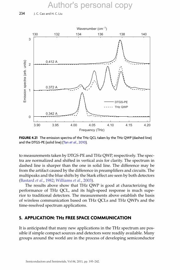
JAGADISH Ch04-9780123813374 2011/4/30 11:07 Page 234 #40
234 J. C. Cao and H. C. Liu
130
3
2
1
0
0.412 A
DTGS-PE
THz QWP
0.372 A
0.342 A
Wavenumber (cm−1)
132 134 136 138 140
3.90 3.95 4.00 4.05
Frequency (THz)
Em
issi
on s
pect
ra (
arb.
uni
ts)
4.10 4.204.15
FIGURE 4.21 The emission spectra of the THz QCL taken by the THz QWP (dashed line)and the DTGS-PE (solid line) (Tan et al., 2010).
to measurements taken by DTGS-PE and THz QWP, respectively. The spec-tra are normalized and shifted in vertical axis for clarity. The spectrum indashed line is sharper than the one in solid line. The difference may befrom the artifact caused by the difference in preamplifiers and circuits. Themultipeaks and the blue shifts by the Stark effect are seen by both detectors(Bastard et al., 1982; Williams et al., 2003).
The results above show that THz QWP is good at characterizing theperformance of THz QCL, and its high-speed response is much supe-rior to traditional detectors. The measurements above establish the basisof wireless communication based on THz QCLs and THz QWPs and thetime-resolved spectrum applications.
5. APPLICATION: THz FREE SPACE COMMUNICATION
It is anticipated that many new applications in the THz spectrum are pos-sible if simple compact sources and detectors were readily available. Manygroups around the world are in the process of developing semiconductor
Author's personal copy
Semiconductors and Semimetals, Vol 84, 2011, pp. 195–242.
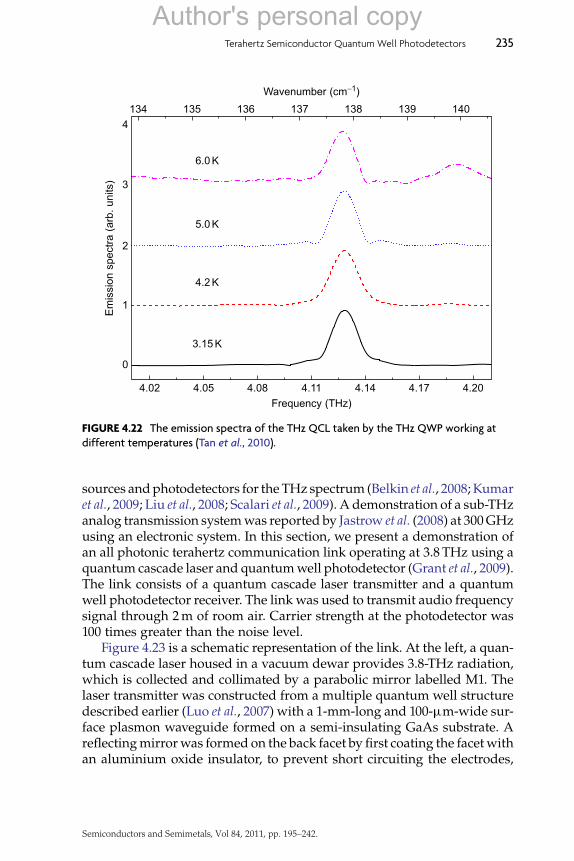
JAGADISH Ch04-9780123813374 2011/4/30 11:07 Page 235 #41
Terahertz Semiconductor Quantum Well Photodetectors 235
134
4
2
Em
issi
on s
pect
ra (
arb.
uni
ts)
1
0
3.15K
4.2K
5.0K
6.0K
3
Wavenumber (cm−1)
135 136 137 138 139 140
4.02 4.05 4.08 4.11
Frequency (THz)
4.14 4.17 4.20
FIGURE 4.22 The emission spectra of the THz QCL taken by the THz QWP working atdifferent temperatures (Tan et al., 2010).
sources and photodetectors for the THz spectrum (Belkin et al., 2008; Kumaret al., 2009; Liu et al., 2008; Scalari et al., 2009). A demonstration of a sub-THzanalog transmission system was reported by Jastrow et al. (2008) at 300 GHzusing an electronic system. In this section, we present a demonstration ofan all photonic terahertz communication link operating at 3.8 THz using aquantum cascade laser and quantum well photodetector (Grant et al., 2009).The link consists of a quantum cascade laser transmitter and a quantumwell photodetector receiver. The link was used to transmit audio frequencysignal through 2 m of room air. Carrier strength at the photodetector was100 times greater than the noise level.
Figure 4.23 is a schematic representation of the link. At the left, a quan-tum cascade laser housed in a vacuum dewar provides 3.8-THz radiation,which is collected and collimated by a parabolic mirror labelled M1. Thelaser transmitter was constructed from a multiple quantum well structuredescribed earlier (Luo et al., 2007) with a 1-mm-long and 100-µm-wide sur-face plasmon waveguide formed on a semi-insulating GaAs substrate. Areflecting mirror was formed on the back facet by first coating the facet withan aluminium oxide insulator, to prevent short circuiting the electrodes,
Author's personal copy
Semiconductors and Semimetals, Vol 84, 2011, pp. 195–242.

JAGADISH Ch04-9780123813374 2011/4/30 11:07 Page 236 #42
236 J. C. Cao and H. C. Liu
MP3player
MOD
AMradio
LNA
2m path
77k
M1 M2
FIGURE 4.23 Schematic of link showing quantum cascade laser at left and quantum wellphotodetector on right (Grant et al., 2009).
followed by evaporating a gold layer over the facet. The exit coupler of thelaser is the cleaved surface. M1 is a 50-mm focal length off-axis parabolicreflector, whereas M2 is 76-mm focal length. Both mirrors are 50 mm indiameter. The laser was mounted on an aluminum cold finger in a liquidnitrogen dewar with the laser facet approximately 2 mm from the low-density polyethylene window. This permitted collecting a large fraction ofthe diverging beam with an off-axis parabolic mirror. A temperature sen-sor was mounted near the base of the QCL die and showed that the basetemperature was maintained at 78 or 77 K.
Care was required to align the four optical components, the QCL,the QWIP, and the two mirrors. The initial alignment was performed inair without the polyethylene windows. The photodetector was displacedby 2 mm using a translation stage and a visible laser beam was passedthrough the photodetector location to the two mirrors and then to the laser.Crude alignment was performed to ensure that the laser was near the focusof each mirror and that the visible light was arriving at the QCL facet. Theoptical coupling was quite sensitive to the position of the QCL which wasrather small. Sometimes, no coupling could be established after an opticalcomponent was moved, and we used a piece of 50-mm diameter Plexiglasspipe 200 cm long as a light guide. The QCL could then be focused on theend of the light pipe, which was only 10 cm away from the mirror. Aftera signal was established, the light guide could be removed, and there was
Author's personal copy
Semiconductors and Semimetals, Vol 84, 2011, pp. 195–242.

JAGADISH Ch04-9780123813374 2011/4/30 11:07 Page 237 #43
Terahertz Semiconductor Quantum Well Photodetectors 237
still sufficient signal to allow optimizing alignment of the long path. Theposition of the larger QW detector was not as critical.
A custom-made electronic pulse generator was fabricated to providelow-duty cycle pulses of amplitude VH. The maximum VH required was17 V at a current of 2.6 A for a peak power of 43 W. The pulse width abovethreshold was approximately 8 ns. Pulse repetition frequency was 455 kHz.Total power injected was calculated from the recorded voltage waveformand integrated to give an average power of 0.16 W or a peak-to-averageratio of 268 : 1. The generator contained power amplifiers that forced VH tofollow the modulation voltage which we wanted to transmit, typically a sinewave at 500 Hz or music. The optimum conditions for VH and modulationamplitude (VM) were found by transmitting a 455-kHz carrier modulatedby a 500-Hz sine wave while measuring the second harmonic at 1 kHz.Clipping by modulating less than threshold or more than saturation rapidlyincreased the second-harmonic content of the detected signal. It was foundthat the best VM was about 1 V peak-to-peak with VH of 15 V.
Numerical calculation of the Fourier transform of the expected pho-tocurrent indicated that there should be a DC term, a modulation term,and a large number of replications of the pulse repetition frequency. Eachreplication would have a carrier plus modulation side-bands. The DC termis proportional to the average laser power and for the low-duty cyclepulses that we are using, the carrier amplitudes are equal to each otherand to the DC term. This is a central point in the demonstration. Eventhough the laser was pulsed, the Fourier transform of the photocurrentcontains useful continuous-wave (CW) components with amplitude equalto the average photocurrent. Further, the modulation side-bands containthe Fourier transform of the time variations of VM.
Experimentally, the 500-Hz basic modulation term could be easilydetected using a bolometer and lock-in amplifier. The 455-kHz pulse rep-etition frequency was also easily detected using the QWIP and could beobserved on a spectrum analyzer as a typical amplitude modulated wave-form. Figure 4.24 shows a typical nonmodulated spectrum measured atthe pulse repetition frequency after the transimpedance amplifier. The leftinset in Fig. 4.24 is an expanded spectrum of the laser measured usingan Fourier transform infrared (FTIR) spectrometer. Both were measuredwhile the QCL was being pulsed at 455 kHz with no modulation. Althoughnone of the modulation can be resolved using the FTIR, the central emis-sion line width is at the FTIR resolution of 0.04 wavenumbers or 1.2 GHz.The right inset shows the QW photodetector spectral responsivity overlaidwith the 126 wavenumber laser spectrum at the left. The RMS photocurrentat the 455 kHz is two orders of magnitude greater than the noise level. Thenoise level from 450 to 460 kHz originates in the custom-made laser driverelectronics and is not a fundamental limitation of the devices. Finally, the
Author's personal copy
Semiconductors and Semimetals, Vol 84, 2011, pp. 195–242.

JAGADISH Ch04-9780123813374 2011/4/30 11:07 Page 238 #44
238 J. C. Cao and H. C. Liu
102
101
100
10−1
10−2
450 455
Frequency (kHz)
Pho
tocu
rren
t (n
A)
460 465
124 126 128 0 100 300 500
Wavenumber Wavenumber
FIGURE 4.24 Spectrum of photocurrent measured after low-noise amplifier with insetsshowing laser spectrum at left and photodetector responsivity at right. Photodetectorspectrum measured at temperature of 12 K (Grant et al., 2009).
signal could be coupled to the antenna input of an AM radio (Sony ICF2010) and music recovered.
The low-noise amplifier (LNA) has a transimpedance amplifier, a fil-ter, and a buffer amplifier, as well as the photodetector bias circuit. Thecapacitance of the cable from the cold section to room temperature wasmeasured as 160 pF plus the large QW photodetector capacitance of 88 pFcaused instability in high-speed amplifiers that we initially tried to use.A general purpose operational amplifier with a 12-MHz gain bandwidthproduct could be made stable in a 1-k� transimpedance configuration.This was followed by a 455-kHz center frequency, 10-kHz bandwidth fil-ter, and a line driver amplifier to provide an effective transimpedance of10 k�. Detector bias was introduced at the input of the transimpedanceamplifier. Typically, our measurements were performed with −20 mV ofbias and 2 µA of total photodetector current. DC photocurrent was alwaysless than 0.1 mA, the resolution of the meter, which was used for moni-toring bias current. Using the QW detector responsivity measured in (Luoet al., 2005) of 1 A/W and the property of the Fourier transform of a narrowpulse (with its low harmonics having the same amplitude as the average),the average optical power can be determined. The recovered 455-kHz car-rier current was 18 nA RMS from which we calculate the average opticalpower to be 1.414× 18 = 25 nW.
Although there are many atmospheric absorption bands known in theTHz frequency region, we observed very little impairment of our linkowing to atmospheric absorption. The center frequency of the laser was
Author's personal copy
Semiconductors and Semimetals, Vol 84, 2011, pp. 195–242.

JAGADISH Ch04-9780123813374 2011/4/30 11:07 Page 239 #45
Terahertz Semiconductor Quantum Well Photodetectors 239
3787 GHz as determined by FTIR measurement of the emission. Empirically,we measured the air in our laboratory in Ottawa, Canada, and observedthat this frequency is at the upper edge of an essentially transparent regionof the electromagnetic spectrum that extends from 3700 to 3789 GHz. Thisband is 89 GHz wide and is only one of many which we observe to beessentially transparent in room air. We point out that while there are manyabsorption bands because of water vapor, as much as 50% of the spectrumspace we observe is transparent or of low absorption. We used a 50-mmdiameter Plexiglass pipe as a gas cell and compared transmission throughroom air with transmission through dry nitrogen and found no difference.The only strong absorber that we observed was liquid water.
6. SUMMARY
We have introduced the principle, simulation and design method, anddevice performance of THz QWPs. At the present time, various incoherentdetection methods (such as bolometer) and several coherent detection meth-ods (such as THz TDS) are well developed and are used in spectroscopyand imaging fields. Because of easy production of high quality and largearea uniform THz QWP materials, THz QWPs have great advantages inhigh sensitivity and high resolution detection, especially in the construc-tion of focal plane arrays. THz QWPs are also useful in the detection oftoxic materials and THz wireless communication. Because the characteris-tic absorption lines of most molecules are in THz range, under a normalcontinuous light source (such as high-voltage mercury lamp), monitoringof toxic materials can be achieved by THz QWPs because of their highspectrum resolution and high response speed. The monitoring ability canbe improved by multicolor THz QWPs, and multiple identifications at thesame time can also be achieved. It can be expected that the developmentof high-performance, single-element detectors and focal plane arrays willenable the THz communication and THz detection applications.
ACKNOWLEDGMENTSWe thank our colleagues and coworkers for their contributions, especially R. Zhang, Z. Y.Tan, X. G. Guo, Y. L. Chen, and F. Xiong in SIMIT, and M. Buchanan, R. Dudek, E. Dupont,M. Graf, P. D. Grant, H. Luo, A. J. SpringThorpe, C. Y. Song, and Z. R. Wasilewski of NationalResearch Council Canada.
REFERENCESAndo, T., Fowler, A. B., and Stern, F. (1982). Rev. Mod. Phys. 54, 437.Bastard, G., Mendez, E. E., Chang, L. L., and Esaki, L. (1982). Phys. Rev. B 28, 3241.Beck, W. A. (1993). Appl. Phys. Lett. 63, 3589.
Author's personal copy
Semiconductors and Semimetals, Vol 84, 2011, pp. 195–242.
JAGADISH Ch04-9780123813374 2011/4/30 11:07 Page 240 #46
240 J. C. Cao and H. C. Liu
Belkin, M. A., Fan, J. A., Hormoz, S., Capasso, F., Khanna, S. P., Lachab, M., Davies, A. G., andLinfield, H. (2008). Opt. Express 16, 3242.
Blakemore, J. S. (1982). J. Appl. Phys. 53, R123.Byer, N. E., Stokowski, S. E., and Venables, J. D. (1975). Appl. Phys. Lett. 27, 639.Cao, J. C. (2006). Physics 35, 953.Cao, J. C., Chen, Y. L., and Liu, H. C. (2006). Superlattices Microstruct. 40, 119.Celik, H., Cankurtaran, M., and Altunoz, S. (2008). Superlattices and Microstruct. 44(2), 237.Cellek, O. O., and Besikci, C. (2004). Semicond. Sci. Technol. 19, 183.Cellek, O. O., Memis, S., Bostanci, U., Ozer, S., and Besikci, C. (2004). Physica E 24, 318.Chen, R. T., Rana, V., and Spitzer, W. G. (1980). J. Appl. Phys. 51, 1532.Chen, Y. L., Guo, X. G., and Cao, J. C. (2006). Chin. Phys. Lett. 23, 1615.Downey, P. M., Jeffries, A. D., Meyer, S. S., Weiss, R., Bachner, F. J., Donnelly, J. P., Lindley,
W. T., Mountain, R. W., and Silversmith, D. J. (1984). Appl. Opt. 23, 910.Ershov, M. (1996). Appl. Phys. Lett. 69, 3480.Ershov, M. (1998). Appl. Phys. Lett. 73, 3432.Ershov, M., Hamaguchi, C., and Ryzhii, V. (1996). Jpn. J. Appl. Phys. 35, 1395.Ershov, M., Liu, H. C., Buchanan, M., Wasilewski, Z. R., and Ryzhii, V. (1997a). Appl. Phys.
Lett. 70, 414.Ershov, M., Liu, H. C., Li, L., Buchanan, M., Wasilewski, Z. R., and Ryzhii, V. (1997b). Appl.
Phys. Lett. 70, 1828.Ershov, M., Ryzhii, V., and Hamaguchi, C. (1995). Appl. Phys. Lett. 67, 3147.Ershov, M., Satou, S., and Ikebe, Y. (1999). J. Appl. Phys. 86, 6642.Fathololoumi, S., Dupont, E., Ban, D., Graf, M., Laframboise, S. R., Wasilewski, Z. R., and Liu,
H. C. (2010). IEEE J. Quantum Electron. 46, 396.Ferguson, B., and Zhang, X. C. (2002). Nat. Mater. 1, 26.Fu, Y., Willander, M., Jiang, J., Li, N., Lu, W., and Liu, H. C. (2003). J. Appl. Phys. 93, 9432.Fukada, E., and Furukawa, T. (1981). Ultrasonics 19, 31.Fung, S., Panda, S., and Panda, B. K. (1999). J. Phys. Condens. Matter 11, 1353.Gornik, E. (1984). Physica B+C 127, 95.Goss, A. J., Nixon, R. D., Watton, R., and Wreathall, W. M. (1984). GEC J. Res. 2, 198.Graf, M., Dupont, E., Luo, H., Haffouz, S., Wasilewski, Z. R., SpringThorpe, A. J., Ban, D., and
Liu, H. C. (2009). Infrared Phys. Technol. 52, 289.Graf, M., Scalari, G., Hofstetter, D., Faist, J., Beere, H., Linfield, E., Ritchie, D., and Davies, G.
(2004). Appl. Phys. Lett. 84, 475.Grant, P. D., Laframboise, S. R., Dudek, R., Graf, M., Bezinger, A., and Liu, H. C. (2009).
Electron. Lett. 45, 952.Gunapala, S. D., Bandara, S. V., Liu, J. K., Hill, C. J., Rafol, S. B., Mumolo, J. M., Trinh, J. T.,
Tidrow, M. Z., and Levan, P. D. (2005). Proc. SPIE 5783, 789.Gunapala, S. D., Bandara, S. V., Singh, A., Liu, J. K., Rafol, S. B., Luong, E. M., Mumolo, J. M.,
Tran, N. Q., Ting, D. Z. Y., Vincent, J. D., Shott, C. A., Long, J., and LeVan, P. D. (2000). IEEETrans. Electron Devices 47, 963.
Gunnarsson, O., and Lundqvist, B. I. (1976). Phys. Rev. B 13, 4274.Guo, X. G., Tan, Z. Y., Cao, J. C., and Liu, H. C. (2009). Appl. Phys. Lett. 94, 201101.Haller, E. E. (1994). Infrared Phys. Technol. 35, 127.Haller, E. E., Hueschen, M. R., and Richards, P. L. (1979). Appl. Phys. Lett. 34, 495.Heitmann, D., Kotthaus, J. P., and Mohr, E. G. (1982). Solid State Commun. 44, 715.Helm, M. (2000). The basic physics of intersubband transitions. in: “Intersubband Transition
in Quantum Wells: Physics and Device Applications I”, edited by Liu, H. C., and Capasso,F., Academic, San Diego, CA.
Hewageegana, P., and Apalkov, V. (2008). Infrared Phys. Technol. 51, 550.Hosako, I., Sekine, N., Patrashin, M., and Yasuda, H. (2007). Proc. SPIE 6772, 67720R.
Author's personal copy
Semiconductors and Semimetals, Vol 84, 2011, pp. 195–242.

JAGADISH Ch04-9780123813374 2011/4/30 11:07 Page 241 #47
Terahertz Semiconductor Quantum Well Photodetectors 241
Ikonic, Z., Milanovic, V., and Tjapkin, D. (1989). Appl. Phys. Lett. 54, 247.Jastrow, C., Munter, K., Piesiewicz, R., Kurner, T., Koch, M., and Kleine-Ostmann, T. (2008).
Electron. Lett. 44, 213.Jovanovic, V. D., Harrison, P., Ikonic, Z., and Indjin, D. (2004). J. Appl. Phys. 96, 269.Kane, M. J., Millidge, S., Emeny, M. T., Lee, D., Guy, D. R. P., and Whitehouse, C. R. (1992).
in: “Intersubband Transitions in Quantum Wells.” edited by Rosencher, E., Vinter, B., andLevine, B. F., (Plenum, New York), pp. 31–42.
Klingshirm, C. F. (1997). “Semiconductor Optics.” Springger-Verlag, Berlin.Kumar, S., Hu, Q., and Reno, J. L. (2009). Appl. Phys. Lett. 94, 131105.Lake, R., Klimeck, G., Bowen, R. C., and Jovanovic, D. (1997). J. Appl. Phys. 81, 7845.Lal, R. B., and Batra, A. K. (1993). Ferroelectrics 142, 51.Levine, B. F. (1993). J. Appl. Phys. 74, R1.Levine, B. F., Bethea, C. G., Hasnain, G., Shen, V. O., Pelve, E., Abbott, R. R., and Hsieh, S. J.
(1990). Appl. Phys. Lett. 56, 851.Levine, B. F., Choi, K. K., Bethea, C. G., Walker, J., and Malik, R. J. (1987). Appl. Phys. Lett. 50,
1092.Li, H., Cao, J. C., Han, Y. J., Tan, Z. Y., and Guo, X. G. (2009a). J. Phys. D Appl. Phys. 42,
205102.Li, H., Cao, J. C., Tan, Z. Y., Han, Y. J., Guo, X. G., Feng, S. L., Luo, H., Laframboise, S. R., and
Liu, H. C. (2009b). J. Phys. D Appl. Phys. 42, 025101.Liu, A. (1994). Phys. Rev. B 50, 8569.Liu, H. C. (1992). Appl. Phys. Lett. 60, 1507.Liu, H. C. (1993). J. Appl. Phys. 73, 3062.Liu, H. C., Buchanan, M., Wasilewski, Z. R., and Chu, H. (1991). Appl. Phys. Lett. 58,
1059.Liu, H. C., and Capasso, F. (2000). “Intersubband Transitions in Quantum wells: Physics and
Device Application I.” Academic Press, San Diego.Liu, H. C., Li, L., Buchanan, M., and Wasilewski, Z. R. (1997). J. Appl. Phys. 82, 889.Liu, H. C., Luo, H., Song, C. Y., Wasilewski, Z. R., SpringThorpe, A. J., and Cao, J. C. (2007a).
Infrared Phys. Technol. 50, 191.Liu, H. C., Luo, H., Song, C. Y., Wasilewski, Z. R., Thorpe, A. J. S., and Cao, J. C. (2007b).
Infrared Phys. Technol. 50, 191.Liu, H. C., Luo, H., Song, C. Y., Wasilewski, Z. R., Thorpe, A. J. S., and Cao, J. C. (2008). IEEE
J. Sel. Top. Quantum Electron. 14, 374.Liu, H. C., Song, C. Y., SpringThorpe, A. J., and Cao, J. C. (2004). Appl. Phys. Lett. 84, 4068.Liu, H. C., Song, C. Y., Wasilewski, Z. R., SpringThorpe, A. J., Cao, J. C., Dharma-wardana,
C., Aers, G. C., Lockwood, D. J., and Gupta, J. A. (2003). Phys. Rev. Lett. 90, 077402.Luo, H., Laframboise, S. R., Wasilewski, Z. R., Aers, G. C., Liu, H. C., and Cao, J. C. (2007).
Appl. Phys. Lett. 90, 041112.Luo, H., Liu, H. C., Song, C. Y., and Wasilewski, Z. R. (2005). Appl. Phys. Lett. 86, 231103.Luo, H., Liu, H. C., Song, C. Y., Wasilewski, Z. R., and SpringThorpe, A. J. (2006). Proc. SPIE
6386, 638611.Patrashin, M., and Hosako, I. (2008). Opt. Lett. 33, 168.Patrashin, M., Hosako, I., and Merken, P. (2006). Proc. SPIE 6038, 60380H.Perera, A. G. U. (2006). Opto-electron. Rev. 14, 103.Perera, A. G. U., Shen, W. Z., Liu, H. C., Buchanan, M., and Schaff, W. J. (2000). Mat. Sci. Eng.
B-SOLID 74, 56.Petrov, A., and Shik, A. (1998). J. Appl. Phys. 83, 3203.Richards, P. L. (1994). J. Appl. Phys. 76, 1.Ryzhii, M., and Ryzhii, V. (1998). Appl. Phys. Lett. 72, 842.Ryzhii, M., Ryzhii, V., and Willander, M. (1998). J. Appl. Phys. 84, 3403.
Author's personal copy
Semiconductors and Semimetals, Vol 84, 2011, pp. 195–242.

JAGADISH Ch04-9780123813374 2011/4/30 11:07 Page 242 #48
242 J. C. Cao and H. C. Liu
Ryzhii, V. (1997). J. Appl. Phys. 81, 6442.Scalari, G., Walther, C., Fischer, M., Terazzi, R., Beere, H., Ritchie, D., and Faist, J. (2009). Laser
& Photon. Rev. 3, 45.Schneider, H., Fleissner, J., Rehm, R., Walther, M., Pletschen, W., Koidl, P., Weimann, G.,
Ziegler, J., Breiter, R., and Cabanski, W. A. (2003). Proc. SPIE 4820, 297.Schneider, H., Koidl, P., Schonbein, C., Ehret, S., Larkins, E. C., and Bihlmann, G. (1996).
Superlattices Microstruct. 19, 347.Schneider, H., and Liu, H. C. (2006). “Quantum well infrared photodetectors: Physics and
applications.” Springer, Berlin.Schneider, H., Liu, H. C., Winnerl, S., Song, C. Y., Walther, M., and Helm, M. (2009). Opt.
Express 17, 12279.Schneider, H., Schonbein, C., Walther, M., Schwarz, K., Fleissner, J., and Koidl, P. (1997). Appl.
Phys. Lett. 71, 246.Schonbein, C., Schneider, H., Bihlmann, G., Schwarz, K., and Koidl, P. (1996). Appl. Phys. Lett.
68, 973.Shen, Y. R. (1984). “The principles of nonlinear optics.” John Wiely & Sons, New York.Spitzer, W. G., and Panish, M. B. (1969). J. Appl. Phys. 40, 4200.Stillman, G. E., Wolfe, C. M., and Dimmock, J. O. (1970). J. Phys. Chem. Solids 31, 1199.Tan, Z. Y., and Cao, J. C. (2008). Physics 37, 199.Tan, Z. Y., Guo, X. G., Cao, J. C., Li, H., and Han, Y. J. (2010). Acta Phys. Sin. 59, 2391.Tan, Z. Y., Guo, X. G., Cao, J. C., Li, H., Wang, X., Feng, S. L., Wasilewski, Z. R., and Liu, H. C.
(2009). Semicond. Sci. Technol. 24, 115014.Thibaudeau, L., Bois, P., and Duboz, J. Y. (1996). J. Appl. Phys. 79, 446.Todorov, Y., and Minot, C. (2007). J. Opt. Soc. Am. A 24, 3100.Tonouchi, M. (2007). Nat. Photon. 1, 97.West, L. C., and Eglash, S. J. (1985). Appl. Phys. Lett. 46, 1156.Williams, B. S., Callebaut, H., Kumar, S., Hu, Q., and Reno, J. L. (2003). Appl. Phys. Lett. 82,
1015.Xiong, F., Guo, X. G., and Cao, J. C. (2008). Chin. Phys. Lett. 25, 1895.Yang, J., Ruan, S. C., and Zhang, M. (2008). Chin. Opt. Lett. 6, 29.Yang, Y., Liu, H. C., Shen, W. Z., Li, N., Lu, W., Wasilewski, Z. R., and Buchanan, M. (2009).
IEEE J. Quantum Electron. 45, 623.Załuzny, M. (1993). Phys. Rev. B 47, 3995.Zhang, J., and Potz, W. (1990). Phys. Rev. B 42, 11366.Zhang, R., Guo, X. G., and Cao, J. C. (2011). Acta Phys. Sin. 60, in press.
Author's personal copy
Semiconductors and Semimetals, Vol 84, 2011, pp. 195–242.