Embed Size (px)
Citation preview
Aurora 64B/66B v12.0
LogiCORE IP Product Guide
Vivado Design SuitePG074 May 22, 2019
Aurora 64B/66B v12.0 2PG074 May 22, 2019 www.xilinx.com
Table of ContentsIP Facts
Chapter 1: OverviewApplications . . . . . . . . . . . . . . . . . . . . . . . . . . . . . . . . . . . . . . . . . . . . . . . . . . . . . . . . . . . . . . . . . . . . . . 6Unsupported Features. . . . . . . . . . . . . . . . . . . . . . . . . . . . . . . . . . . . . . . . . . . . . . . . . . . . . . . . . . . . . . 7Licensing and Ordering . . . . . . . . . . . . . . . . . . . . . . . . . . . . . . . . . . . . . . . . . . . . . . . . . . . . . . . . . . . . . 7
Chapter 2: Product SpecificationPerformance. . . . . . . . . . . . . . . . . . . . . . . . . . . . . . . . . . . . . . . . . . . . . . . . . . . . . . . . . . . . . . . . . . . . . . 9Resource Utilization. . . . . . . . . . . . . . . . . . . . . . . . . . . . . . . . . . . . . . . . . . . . . . . . . . . . . . . . . . . . . . . 11Port Descriptions . . . . . . . . . . . . . . . . . . . . . . . . . . . . . . . . . . . . . . . . . . . . . . . . . . . . . . . . . . . . . . . . . 12
Chapter 3: Designing with the CoreGeneral Design Guidelines . . . . . . . . . . . . . . . . . . . . . . . . . . . . . . . . . . . . . . . . . . . . . . . . . . . . . . . . . 62Clocking. . . . . . . . . . . . . . . . . . . . . . . . . . . . . . . . . . . . . . . . . . . . . . . . . . . . . . . . . . . . . . . . . . . . . . . . . 63Reset and Power Down . . . . . . . . . . . . . . . . . . . . . . . . . . . . . . . . . . . . . . . . . . . . . . . . . . . . . . . . . . . . 67Shared Logic . . . . . . . . . . . . . . . . . . . . . . . . . . . . . . . . . . . . . . . . . . . . . . . . . . . . . . . . . . . . . . . . . . . . . 74Using CRC . . . . . . . . . . . . . . . . . . . . . . . . . . . . . . . . . . . . . . . . . . . . . . . . . . . . . . . . . . . . . . . . . . . . . . . 76Hot Plug Logic. . . . . . . . . . . . . . . . . . . . . . . . . . . . . . . . . . . . . . . . . . . . . . . . . . . . . . . . . . . . . . . . . . . . 76Clock Compensation Logic. . . . . . . . . . . . . . . . . . . . . . . . . . . . . . . . . . . . . . . . . . . . . . . . . . . . . . . . . . 77Using Little Endian Support . . . . . . . . . . . . . . . . . . . . . . . . . . . . . . . . . . . . . . . . . . . . . . . . . . . . . . . . . 78
Chapter 4: Design Flow StepsCustomizing and Generating the Core . . . . . . . . . . . . . . . . . . . . . . . . . . . . . . . . . . . . . . . . . . . . . . . . 79 Constraining the Core . . . . . . . . . . . . . . . . . . . . . . . . . . . . . . . . . . . . . . . . . . . . . . . . . . . . . . . . . . . . . 95Simulation . . . . . . . . . . . . . . . . . . . . . . . . . . . . . . . . . . . . . . . . . . . . . . . . . . . . . . . . . . . . . . . . . . . . . . 99Synthesis and Implementation . . . . . . . . . . . . . . . . . . . . . . . . . . . . . . . . . . . . . . . . . . . . . . . . . . . . . 100
Chapter 5: Example DesignDirectory and File Contents. . . . . . . . . . . . . . . . . . . . . . . . . . . . . . . . . . . . . . . . . . . . . . . . . . . . . . . . 101Quick Start Example Design . . . . . . . . . . . . . . . . . . . . . . . . . . . . . . . . . . . . . . . . . . . . . . . . . . . . . . . 101Detailed Example Design. . . . . . . . . . . . . . . . . . . . . . . . . . . . . . . . . . . . . . . . . . . . . . . . . . . . . . . . . . 103
Send Feedback
Aurora 64B/66B v12.0 3PG074 May 22, 2019 www.xilinx.com
Using Vivado Lab Tools . . . . . . . . . . . . . . . . . . . . . . . . . . . . . . . . . . . . . . . . . . . . . . . . . . . . . . . . . . . 106Implementing the Example Design. . . . . . . . . . . . . . . . . . . . . . . . . . . . . . . . . . . . . . . . . . . . . . . . . . 106Hardware Reset FSM in the Example Design . . . . . . . . . . . . . . . . . . . . . . . . . . . . . . . . . . . . . . . . . . 106
Chapter 6: Test Bench
Appendix A: Verification, Compliance, and Interoperability
Appendix B: UpgradingDevice Migration . . . . . . . . . . . . . . . . . . . . . . . . . . . . . . . . . . . . . . . . . . . . . . . . . . . . . . . . . . . . . . . . 113Upgrading in the Vivado Design Suite . . . . . . . . . . . . . . . . . . . . . . . . . . . . . . . . . . . . . . . . . . . . . . . 114Migrating Legacy (LocalLink based) Aurora 64B/66B Cores to the AXI4-Stream Aurora 64B/66B Core
116
Appendix C: DebuggingFinding Help on Xilinx.com . . . . . . . . . . . . . . . . . . . . . . . . . . . . . . . . . . . . . . . . . . . . . . . . . . . . . . . . 123Vivado Design Suite Debug Feature . . . . . . . . . . . . . . . . . . . . . . . . . . . . . . . . . . . . . . . . . . . . . . . . . 125Simulation Debug. . . . . . . . . . . . . . . . . . . . . . . . . . . . . . . . . . . . . . . . . . . . . . . . . . . . . . . . . . . . . . . . 125Hardware Debug . . . . . . . . . . . . . . . . . . . . . . . . . . . . . . . . . . . . . . . . . . . . . . . . . . . . . . . . . . . . . . . . 127Design Bring-Up on the KC705 Evaluation Board . . . . . . . . . . . . . . . . . . . . . . . . . . . . . . . . . . . . . . 133Interface Debug . . . . . . . . . . . . . . . . . . . . . . . . . . . . . . . . . . . . . . . . . . . . . . . . . . . . . . . . . . . . . . . . . 133
Appendix D: Generating a GT Wrapper File from the Transceiver Wizard
Appendix E: Additional Resources and Legal NoticesXilinx Resources . . . . . . . . . . . . . . . . . . . . . . . . . . . . . . . . . . . . . . . . . . . . . . . . . . . . . . . . . . . . . . . . . 135Documentation Navigator and Design Hubs . . . . . . . . . . . . . . . . . . . . . . . . . . . . . . . . . . . . . . . . . . 135References . . . . . . . . . . . . . . . . . . . . . . . . . . . . . . . . . . . . . . . . . . . . . . . . . . . . . . . . . . . . . . . . . . . . . 135Revision History . . . . . . . . . . . . . . . . . . . . . . . . . . . . . . . . . . . . . . . . . . . . . . . . . . . . . . . . . . . . . . . . . 137Please Read: Important Legal Notices . . . . . . . . . . . . . . . . . . . . . . . . . . . . . . . . . . . . . . . . . . . . . . . 141
Send Feedback
Aurora 64B/66B v12.0 4PG074 May 22, 2019 www.xilinx.com Product Specification
IntroductionThe Xilinx® LogiCORE™ IP Aurora 64B/66B core is a scalable, lightweight, high data rate, link-layer protocol for high-speed serial communication. The protocol is open and can be implemented using Xilinx device technology.
The Vivado® Design Suite produces source code for Aurora 64B/66B cores. The cores can be simplex or full-duplex, and feature one of two simple user interfaces and optional flow control.
Features• General-purpose data channels with
throughput range from 500 Mb/s to over 400 Gb/s
• Supports up to 16 consecutively bonded 7 series GTX/GTH, UltraScale™ GTH/GTY or UltraScale+™ GTH/GTY transceivers
• The GT subcore is also available outside the Aurora core
• Aurora 64B/66B protocol specification v1.3 compliant (64B/66B encoding)
• Low resource cost with very low (3%) transmission overhead
• Easy-to-use AXI4-Stream based framing and flow control interfaces
• Automatically initializes and maintains the channel
• Full-duplex or simplex operation• 32-bit Cyclic Redundancy Check (CRC) for
user data • Added support for the Simplex Auto Link
Recovery feature• Supports RX polarity inversion• Big endian/little endian AXI4-Stream user
interface• Fully compliant AXI4-Lite DRP interface• Configurable DRP, INIT clock• Single-ended or differential clocking
options for GTREFCLK and core INIT_CLK
IP Facts
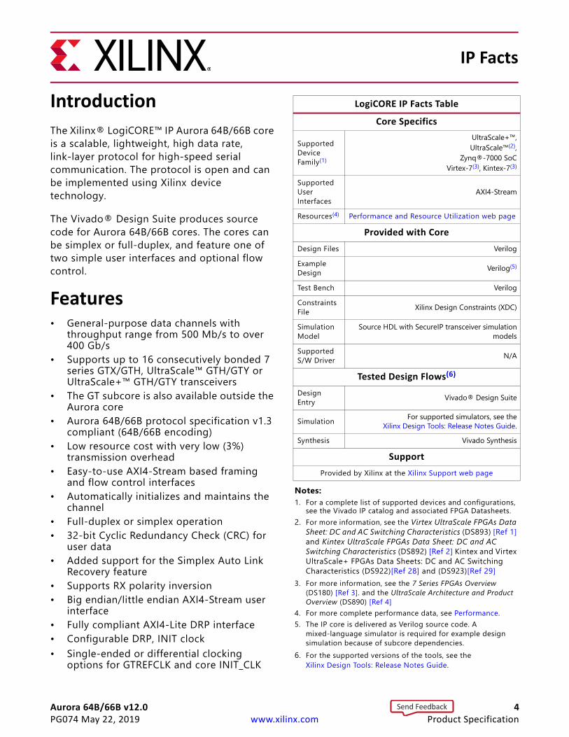
LogiCORE IP Facts TableCore Specifics
Supported Device Family(1)
UltraScale+™,UltraScale™(2),
Zynq®-7000 SoCVirtex-7(3), Kintex-7(3)
Supported User Interfaces
AXI4-Stream
Resources(4) Performance and Resource Utilization web page
Provided with CoreDesign Files VerilogExample Design Verilog(5)
Test Bench VerilogConstraints File Xilinx Design Constraints (XDC)
Simulation Model
Source HDL with SecureIP transceiver simulationmodels
Supported S/W Driver N/A
Tested Design Flows(6)
Design Entry Vivado® Design Suite
Simulation For supported simulators, see theXilinx Design Tools: Release Notes Guide.
Synthesis Vivado Synthesis
SupportProvided by Xilinx at the Xilinx Support web page
Notes: 1. For a complete list of supported devices and configurations,
see the Vivado IP catalog and associated FPGA Datasheets.2. For more information, see the Virtex UltraScale FPGAs Data
Sheet: DC and AC Switching Characteristics (DS893) [Ref 1] and Kintex UltraScale FPGAs Data Sheet: DC and AC Switching Characteristics (DS892) [Ref 2] Kintex and Virtex UltraScale+ FPGAs Data Sheets: DC and AC Switching Characteristics (DS922)[Ref 28] and (DS923)[Ref 29]
3. For more information, see the 7 Series FPGAs Overview (DS180) [Ref 3]. and the UltraScale Architecture and Product Overview (DS890) [Ref 4]
4. For more complete performance data, see Performance.5. The IP core is delivered as Verilog source code. A
mixed-language simulator is required for example design simulation because of subcore dependencies.
6. For the supported versions of the tools, see the Xilinx Design Tools: Release Notes Guide.
Send Feedback
Aurora 64B/66B v12.0 5PG074 May 22, 2019 www.xilinx.com
Chapter 1
OverviewThis product guide describes the function and operation of the LogiCORE™ IP Aurora 64B/66B core and provides information about designing, customizing, and implementing the core.
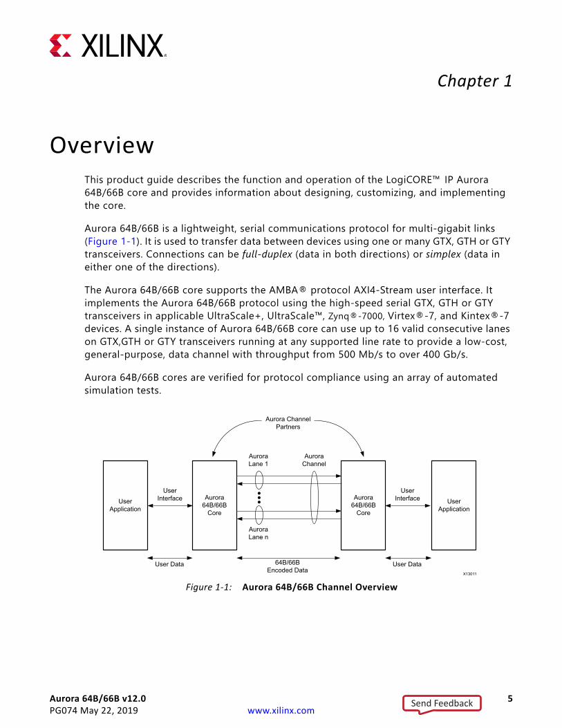
Aurora 64B/66B is a lightweight, serial communications protocol for multi-gigabit links (Figure 1-1). It is used to transfer data between devices using one or many GTX, GTH or GTY transceivers. Connections can be full-duplex (data in both directions) or simplex (data in either one of the directions).
The Aurora 64B/66B core supports the AMBA® protocol AXI4-Stream user interface. It implements the Aurora 64B/66B protocol using the high-speed serial GTX, GTH or GTY transceivers in applicable UltraScale+, UltraScale™, Zynq®-7000, Virtex®-7, and Kintex®-7 devices. A single instance of Aurora 64B/66B core can use up to 16 valid consecutive lanes on GTX,GTH or GTY transceivers running at any supported line rate to provide a low-cost, general-purpose, data channel with throughput from 500 Mb/s to over 400 Gb/s.
Aurora 64B/66B cores are verified for protocol compliance using an array of automated simulation tests.X-Ref Target - Figure 1-1
Figure 1-1: Aurora 64B/66B Channel Overview
User Application
Aurora64B/66B
Core
Aurora64B/66B
Core
User Application
User Interface
User Data
Aurora Lane 1
Aurora Channel
Aurora Lane n
User Interface
User Data64B/66B Encoded Data
Aurora ChannelPartners
X13011
Send Feedback
Aurora 64B/66B v12.0 6PG074 May 22, 2019 www.xilinx.com
Chapter 1: Overview
Aurora 64B/66B cores automatically initialize a channel when they are connected to an Aurora 64B/66B channel partner. After initialization, applications can pass data across the channel as frames or streams of data. Aurora 64B/66B frames can be of any size, and can be interrupted any time by high priority requests. Gaps between valid data bytes are automatically filled with idles to maintain lock and prevent excessive electromagnetic interference. Flow control is optional in Aurora 64B/66B, and can be used to throttle the link partner transmit data rate, or to send brief, high-priority messages through the channel.
Streams are implemented in Aurora 64B/66B as a single, unending frame. Whenever data is not being transmitted, idles are transmitted to keep the link alive. Excessive bit errors, disconnections, or equipment failures cause the core to reset and attempt to initialize a new channel. The Aurora 64B/66B core can support a maximum of two symbols skew in the receipt of a multi-lane channel. The Aurora 64B/66B protocol uses 64B/66B encoding. The 64B/66B encoding offers theoretical improved performance because of its very low (3%) transmission overhead, compared to 25% overhead for 8B/10B encoding.
RECOMMENDED:1. Although the Aurora 64B/66B core is a fully-verified solution, the challenge associated with
implementing a complete design varies depending on the configuration and functionality of theapplication. For best results, prior experience in building high-performance, pipelined FPGA designsusing Xilinx implementation tools and Xilinx® Design Constraints (XDC) user constraints files isrecommended.
2. Consult the PCB design requirements information in the UltraScale FPGAs GTH Transceivers UserGuide (UG576) [Ref 5], UltraScale FPGAs GTY Transceivers User Guide (UG578) [Ref 6], and 7 Series FPGAs GTX/GTH Transceivers User Guide (UG476) [Ref 7].Contact your local Xilinx representative for a closer review and estimation for your specificrequirements.
ApplicationsAurora 64B/66B cores can be used in a wide variety of applications because of their low resource cost, scalable throughput, and flexible data interface. Examples of Aurora 64B/66B core applications include:
• Chip-to-chip links: Replacing parallel connections between chips with high-speed serial connections can significantly reduce the number of traces and layers required on a PCB.
• Board-to-board and backplane links: Aurora 64B/66B uses standard 64B/66B encoding, which is the preferred encoding scheme for 10 Gigabit Ethernet, making it compatible with many existing hardware standards for cables and backplanes. Aurora 64B/66B can be scaled, both in line rate and channel width, to allow inexpensive legacy hardware to be used in new, high-performance systems.
Send Feedback
Aurora 64B/66B v12.0 7PG074 May 22, 2019 www.xilinx.com
Chapter 1: Overview
• Simplex connections (unidirectional): The Aurora 64B/66B simplex protocol providesunidirectional channel initialization, making it possible to use the GTX, GTH and GTYtransceivers when a back channel is not available, and to reduce costs due to unusedfull-duplex resources.
Unsupported Features• AXI4-Stream non-strict aligned mode is not supported in the Aurora 64B/66B core.• GTP and GTZ type transceivers of 7 series devices are not supported in the Aurora
64B/66B core.• Aurora 64B/66B supports UFC feature only in GTYE3/GTYE4 devices up to 16.375G.• Dynamic switching of Line rates in case of GTHE4/GTYE4 and CPLL configurations using
DRP's might not work as expected because of the updates made around GTHE4/GTYE4CPLL Calibration module inside the gtwizard_ultrascale IP.
For more information see UltraScale FPGAs Transceivers Wizard (PG182) [Ref 27].
Licensing and OrderingThis Xilinx LogiCORE IP module is provided at no additional cost with the Xilinx Vivado® Design Suite under the terms of the Xilinx End User License. Information about this and other Xilinx LogiCORE IP modules is available at the Xilinx Intellectual Property page. For information about pricing and availability of other Xilinx LogiCORE IP modules and tools, contact your local Xilinx sales representative.
For more information, visit the Aurora 64B/66B product page.
Send Feedback
Aurora 64B/66B v12.0 8PG074 May 22, 2019 www.xilinx.com
Chapter 2
Product SpecificationThe following figure shows a block diagram of the Aurora 64B/66B core.
The major functional modules of the Aurora 64B/66B core are:
• Lane logic: Each GT transceiver is driven by an instance of the lane logic module which initializes each individual transceiver, handles the encoding and decoding of control characters, and performs error detection.
• Global logic: The global logic module in the core performs the channel bonding for channel initialization. During operation, the channel keeps track of the Not Ready idle characters defined by the Aurora 64B/66B protocol and monitors all the lane logic modules for errors.
• RX user interface: The AXI4-Stream receive (RX) user interface moves data from the channel to the application and also performs flow control functions.
• TX user interface: The AXI4-Stream transmit (TX) user interface moves data from the application to the channel and also performs flow control TX functions. The standard clock compensation module is embedded inside the core. This module controls periodic transmission of the clock compensation (CC) character.
X-Ref Target - Figure 2-1
Figure 2-1: Aurora 64B/66B Core Block Diagram
Global Logic (Channel
Maintenance)
Control Interface
X13012
Lane Logic
GTX/GTH/GTY 1
(Lane 1)
Serial I/O Lane 1
RX User Interface
(Framing or Streaming)
Lane Logic
GTX/GTH/GTY 2
(Lane 2)
Serial I/O Lane 2
TX User Interface
(Framing or Streaming)
Lane Logic
GTX/GTH/GTY n
(Lane n)
Serial I/O Lane n
RX Data
TX Data
Aurora Channel Serial I/O
Send Feedback
Aurora 64B/66B v12.0 9PG074 May 22, 2019 www.xilinx.com
Chapter 2: Product Specification
PerformanceThis section details the performance information for various core configurations.
Maximum FrequenciesThe maximum frequency of the core operation is dependent on the line rates supported and the speed grade of the devices.
LatencyFor a default single lane configuration, latency through an Aurora 64B/66B core is caused by pipeline delays through the protocol engine (PE) and through the GTX and GTH transceivers. The PE pipeline delay increases as the AXI4-Stream interface width increases. The transceiver delays are determined by the transceiver features.
This section outlines a method of measuring the latency for the Aurora 64B/66B core AXI4-Stream user interface in terms of user_clk cycles for Zynq®-7000, Virtex®-7, and Kintex®-7 device GTX, GTH transceiver-based designs and UltraScale™, UltraScale+ device GTH and GTY transceiver-based designs. For the purposes of illustrating latency, the Aurora 64B/66B modules are partitioned between logic in the GTX, GTH and GTY transceivers and protocol engine (PE) logic implemented in the FPGA.
Figure 2-2 illustrates the latency of the datapath.
Note: Figure 2-2 does not include the latency incurred due to the length of the serial connection between each side of the Aurora 64B/66B channel.
X-Ref Target - Figure 2-2
Figure 2-2: Latency of the Datapath
TX_PE
X12663
TX AXI Interfaces_axi_tx_tvalid
TX_GT RX_GT RX_PE RX AXI Interfacem_axi_rx_tvalid
Send Feedback
Aurora 64B/66B v12.0 10PG074 May 22, 2019 www.xilinx.com
Chapter 2: Product Specification
The latency must be measured from the rising edge of the transmitter user_clk at the first assertion of s_axi_tx_tvalid and s_axi_tx_tready to the rising edge of the receiver user_clk at the first assertion of m_axi_rx_tvalid. The following figure shows the transmitter and receiver path reference points between which the latency has been measured for the default core configuration.
The following table shows the maximum latency and the individual latency values of the contributing pipeline components for the default core configuration on 7 series GTX, GTH and UltraScale, UltraScale+ GTH transceiver based devices. Latency can vary with the addition of flow controls.
The pipeline delays are designed to maintain the clock speed.
ThroughputAurora 64B/66B core throughput depends on the number of the transceivers, transceiver type, and the target line rate of the transceivers selected. For GTH transceivers, the throughput varies from 0.48 Gb/s to 254.06 Gb/s for a single-lane design to a 16-lane design, respectively. For GTY transceivers, the throughput varies from 0.455 Gb/s to 400 Gb/s with the supported line rate range of 0.5 Gb/s to 25.7813 Gb/s. The maximum throughput for GTY may not be accurate given the lane striping difference in the design when the line rate us greater than 16.375 Gb/s.
X-Ref Target - Figure 2-3
Figure 2-3: Latency Waveform with Reference Points
Table 2-1: Latency for the Default Aurora 64B/66B Core ConfigurationLatency Component user_clk Cycles
Logic 46Gearbox 1 or 2Clock Compensation 7Maximum (total) 54 or 55
Send Feedback
Aurora 64B/66B v12.0 11PG074 May 22, 2019 www.xilinx.com
Chapter 2: Product Specification
Note: Line rate value is restricted to four decimal digits for UltraScale with the exception of 25.78125 Gb/s for GTY devices. See the Aurora Solutions Center for more details specific to the selected configuration.
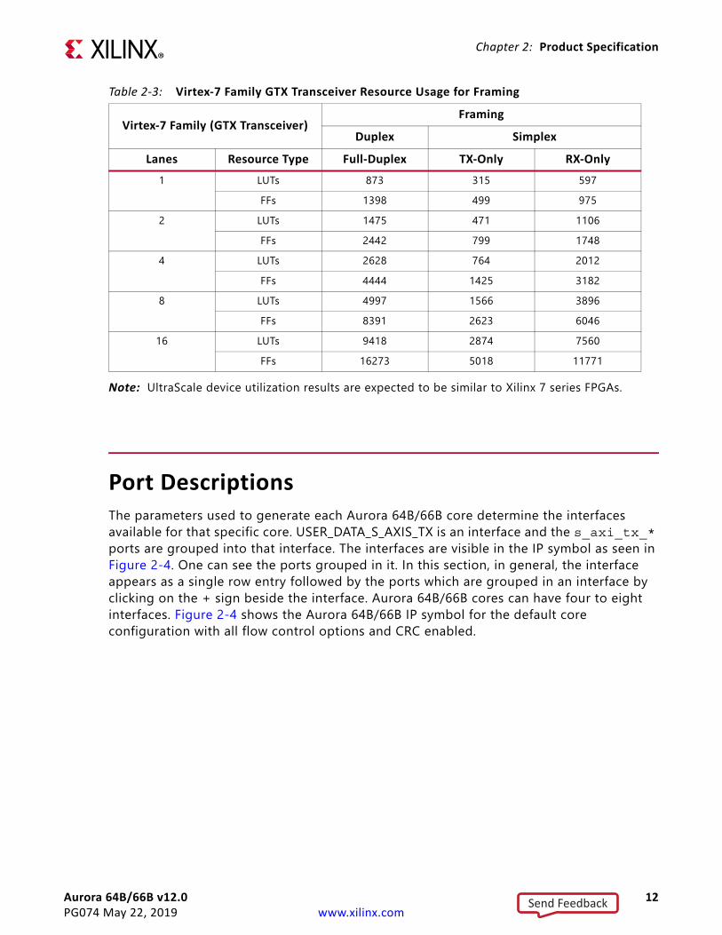
Resource UtilizationFor full details about performance and resource utilization, visit the Performance and Resource Utilization web page. Table 2-2 through Table 2-3 show the number of look-up tables (LUTs) and flip-flops (FFs) used in selected Aurora 64B/66B framing and streaming modules in the Vivado® Design Suite implemented on the xc7vx485tffg1157-1 device. The Aurora 64B/66B core is also available in configurations not shown in the tables. The tables do not include the additional resource usage for flow controls. Resource utilization in the following tables does not include the additional resource usage for the example design modules, such as FRAME_GEN and FRAME_CHECK. Values provided are exact values for a given configuration. Values in the following tables are for the default configuration (3.125G) with support logic included.
Table 2-2: Virtex-7 Family GTX Transceiver Resource Usage for Streaming
Virtex-7 Family (GTX Transceiver)Streaming
Duplex SimplexLanes Resource Type Full-Duplex TX-Only RX-Only
1 LUTs 549 315 377FFs 1359 476 957
2 LUTs 1044 467 686FFs 2379 761 1721
4 LUTs 1971 711 1452FFs 4347 1380 3139
8 LUTs 3610 1256 2805FFs 8219 2539 5973
16 LUTs 6656 1949 5496FFs 15966 4825 11641
Send Feedback
Aurora 64B/66B v12.0 12PG074 May 22, 2019 www.xilinx.com
Chapter 2: Product Specification
Note: UltraScale device utilization results are expected to be similar to Xilinx 7 series FPGAs.
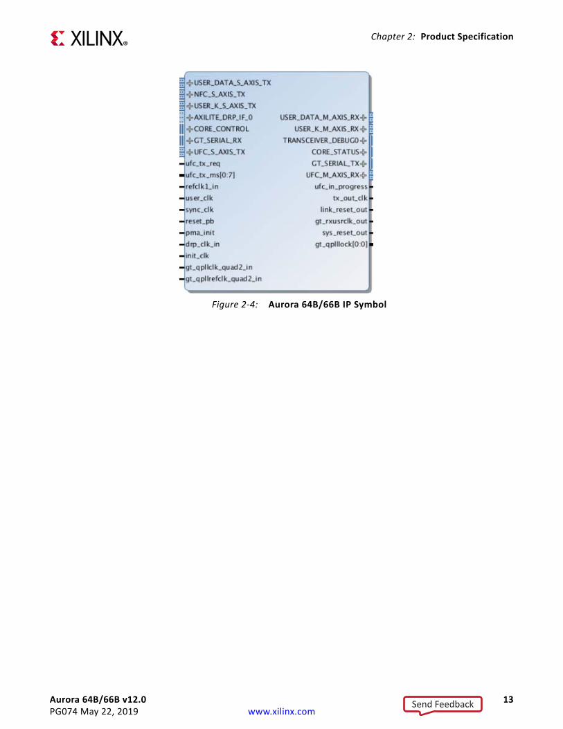
Port DescriptionsThe parameters used to generate each Aurora 64B/66B core determine the interfaces available for that specific core. USER_DATA_S_AXIS_TX is an interface and the s_axi_tx_* ports are grouped into that interface. The interfaces are visible in the IP symbol as seen in Figure 2-4. One can see the ports grouped in it. In this section, in general, the interface appears as a single row entry followed by the ports which are grouped in an interface by clicking on the + sign beside the interface. Aurora 64B/66B cores can have four to eight interfaces. Figure 2-4 shows the Aurora 64B/66B IP symbol for the default core configuration with all flow control options and CRC enabled.
Table 2-3: Virtex-7 Family GTX Transceiver Resource Usage for Framing
Virtex-7 Family (GTX Transceiver)Framing
Duplex SimplexLanes Resource Type Full-Duplex TX-Only RX-Only
1 LUTs 873 315 597FFs 1398 499 975
2 LUTs 1475 471 1106FFs 2442 799 1748
4 LUTs 2628 764 2012FFs 4444 1425 3182
8 LUTs 4997 1566 3896FFs 8391 2623 6046
16 LUTs 9418 2874 7560FFs 16273 5018 11771
Send Feedback
Aurora 64B/66B v12.0 13PG074 May 22, 2019 www.xilinx.com
Chapter 2: Product Specification
X-Ref Target - Figure 2-4
Figure 2-4: Aurora 64B/66B IP Symbol
Send Feedback
Aurora 64B/66B v12.0 14PG074 May 22, 2019 www.xilinx.com
Chapter 2: Product Specification
User InterfaceThe Aurora 64B/66B core can be generated with either a framing or streaming user data interface. Data port width depends on the number of lanes selected. The following table lists simplex/duplex port descriptions for the AXI4-Stream TX data ports.
Table 2-4: User Interface Ports
Name Direction Clock Domain Description
USER_DATA_S_AXIS_TXs_axi_tx_tdata[0:(64n–1)] or s_axi_tx_tdata[(64n–1):0](1)(2) Input user_clk Outgoing data (ascending bit order).
s_axi_tx_tready(2) Output user_clkAsserted when signals from the source are accepted. Deasserted when signals from the source are ignored.
s_axi_tx_tvalid(2) Input user_clkAsserted when AXI4-Stream signals from the source are valid. Deasserted when AXI4-Stream control signals and/or data from the source should be ignored.
s_axi_tx_tlast(2) Input user_clkIndicates the end of the frame.This port is not available if the Streaming interface option is chosen.
s_axi_tx_tkeep[0:(8n–1)] or s_axi_tx_tkeep[(8n–1):0](1)(2) Input user_clk
Specifies the number of valid bytes in the last data beat (number of valid bytes = number of 1s in tkeep). s_axi_tx_tkeep is sampled only when s_axi_tx_tlast is asserted.The core supports continuous aligned and continuous unaligned data streams and expects data to be filled continuously from LSB to MSB. There cannot be invalid bytes interleaved with the valid s_axi_tx_tdata bus.This port is not available if the Streaming interface option is chosen.
USER_DATA_M_AXIS_RXm_axi_rx_tdata[0:(64n–1)] or m_axi_rx_tdata[(64n–1):0](1)(3) Output user_clk Incoming data from channel partner (ascending
bit order).
m_axi_rx_tvalid(3) Output user_clkAsserted when data from core is valid. Deasserted when data from the core should be ignored.
m_axi_rx_tlast(3) Output user_clkIndicates the end of the incoming frame.This port is not available if the Streaming interface option is chosen.
Send Feedback
Aurora 64B/66B v12.0 15PG074 May 22, 2019 www.xilinx.com
Chapter 2: Product Specification
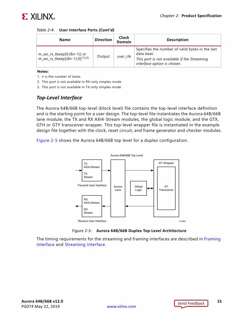
Top-Level Interface
The Aurora 64B/66B top-level (block level) file contains the top-level interface definition and is the starting point for a user design. The top-level file instantiates the Aurora 64B/66B lane module, the TX and RX AXI4-Stream modules, the global logic module, and the GTX, GTH or GTY transceiver wrapper. This top-level wrapper file is instantiated in the example design file together with the clock, reset circuit, and frame generator and checker modules.
Figure 2-5 shows the Aurora 64B/66B top level for a duplex configuration.
The timing requirements for the streaming and framing interfaces are described in Framing Interface and Streaming Interface.
m_axi_rx_tkeep[0:(8n–1)] or m_axi_rx_tkeep[(8n–1):0](1)(3) Output user_clk
Specifies the number of valid bytes in the last data beat.This port is not available if the Streaming interface option is chosen.
Notes: 1. n is the number of lanes.2. This port is not available in RX-only simplex mode.3. This port is not available in TX-only simplex mode
X-Ref Target - Figure 2-5
Figure 2-5: Aurora 64B/66B Duplex Top-Level Architecture
Table 2-4: User Interface Ports (Cont’d)
Name Direction Clock Domain Description
TXAXI4-Stream
TXStream
RXAXI4-Stream
RXStream
Transmit User Interface
Receive User Interface
AuroraLane
GlobalLogic
GTTransceiver
GT Wrapper
Aurora 64B/66B Top Level
X12661
Send Feedback
Aurora 64B/66B v12.0 16PG074 May 22, 2019 www.xilinx.com
Chapter 2: Product Specification
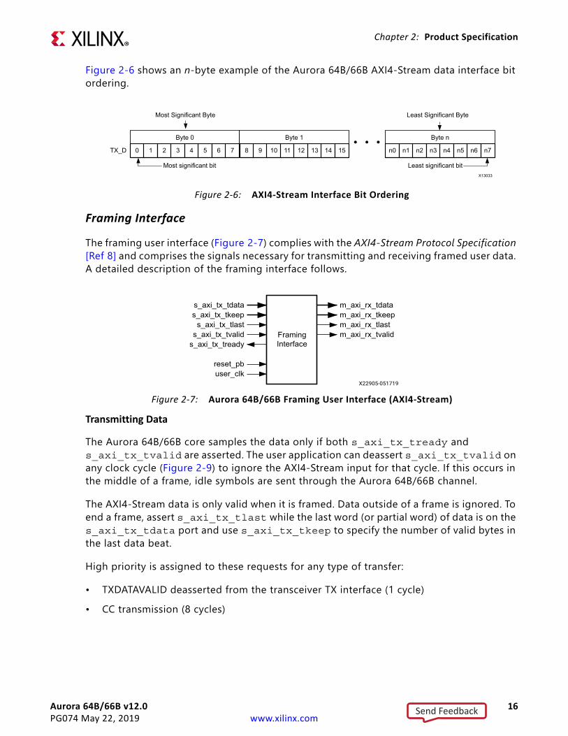
Figure 2-6 shows an n-byte example of the Aurora 64B/66B AXI4-Stream data interface bit ordering.
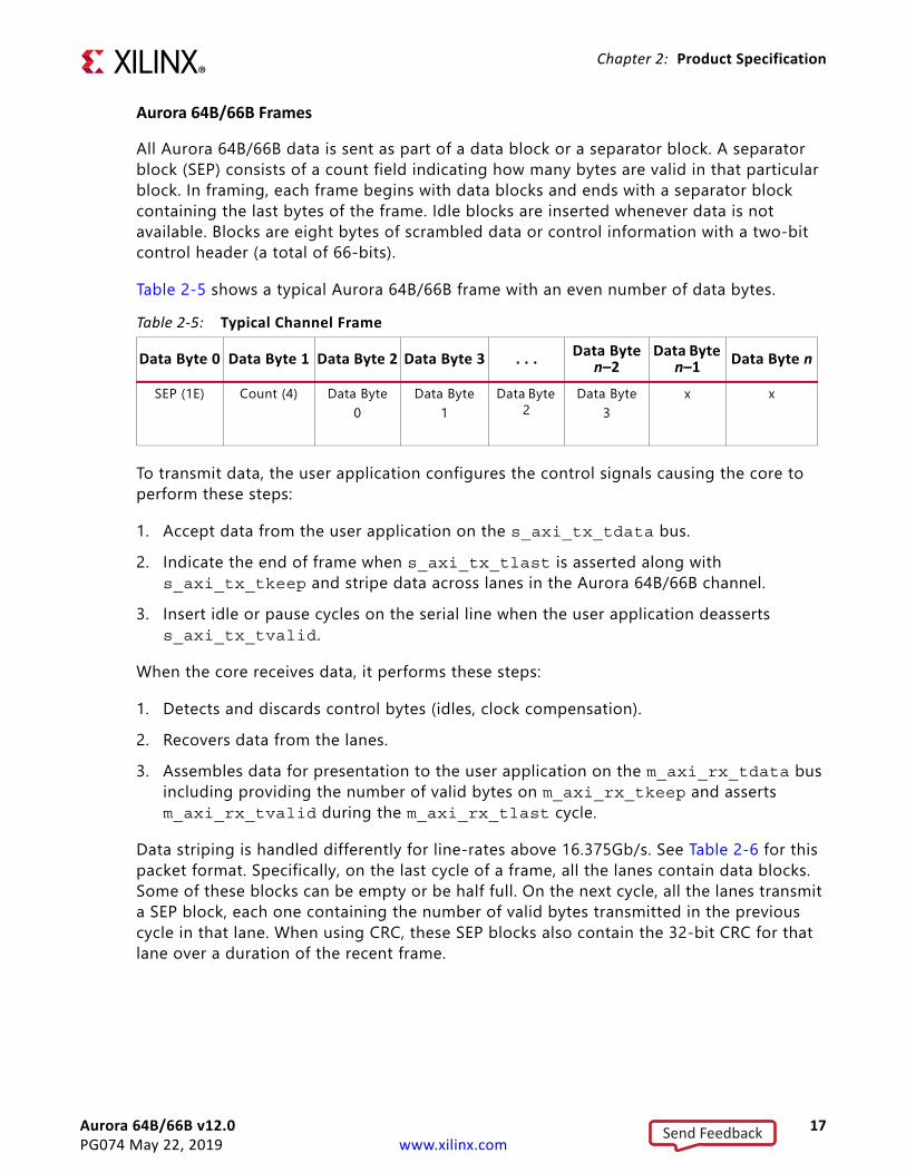
Framing Interface
The framing user interface (Figure 2-7) complies with the AXI4-Stream Protocol Specification [Ref 8] and comprises the signals necessary for transmitting and receiving framed user data. A detailed description of the framing interface follows.
Transmitting Data
The Aurora 64B/66B core samples the data only if both s_axi_tx_tready and s_axi_tx_tvalid are asserted. The user application can deassert s_axi_tx_tvalid on any clock cycle (Figure 2-9) to ignore the AXI4-Stream input for that cycle. If this occurs in the middle of a frame, idle symbols are sent through the Aurora 64B/66B channel.
The AXI4-Stream data is only valid when it is framed. Data outside of a frame is ignored. To end a frame, assert s_axi_tx_tlast while the last word (or partial word) of data is on the s_axi_tx_tdata port and use s_axi_tx_tkeep to specify the number of valid bytes in the last data beat.
High priority is assigned to these requests for any type of transfer:
• TXDATAVALID deasserted from the transceiver TX interface (1 cycle)• CC transmission (8 cycles)
X-Ref Target - Figure 2-6
Figure 2-6: AXI4-Stream Interface Bit Ordering
X-Ref Target - Figure 2-7
Figure 2-7: Aurora 64B/66B Framing User Interface (AXI4-Stream)
0 1 2 3 4 5 6 7 8 9 10 11 12 13 14 15 n0 n1 n2 n3 n4 n5 n6 n7
Byte 0 Byte 1 Byte n
Most Significant Byte Least Significant Byte
TX_D
Most significant bit Least significant bitX13033
Framing Interface
reset_pbuser_clk
s_axi_tx_tdatas_axi_tx_tkeep
s_axi_tx_tlasts_axi_tx_tvalid
s_axi_tx_tready
m_axi_rx_tdatam_axi_rx_tkeepm_axi_rx_tlastm_axi_rx_tvalid
Send Feedback
Aurora 64B/66B v12.0 17PG074 May 22, 2019 www.xilinx.com
Chapter 2: Product Specification
Aurora 64B/66B Frames
All Aurora 64B/66B data is sent as part of a data block or a separator block. A separator block (SEP) consists of a count field indicating how many bytes are valid in that particular block. In framing, each frame begins with data blocks and ends with a separator block containing the last bytes of the frame. Idle blocks are inserted whenever data is not available. Blocks are eight bytes of scrambled data or control information with a two-bit control header (a total of 66-bits).
Table 2-5 shows a typical Aurora 64B/66B frame with an even number of data bytes.
To transmit data, the user application configures the control signals causing the core to perform these steps:
1. Accept data from the user application on the s_axi_tx_tdata bus.2. Indicate the end of frame when s_axi_tx_tlast is asserted along with
s_axi_tx_tkeep and stripe data across lanes in the Aurora 64B/66B channel.3. Insert idle or pause cycles on the serial line when the user application deasserts
s_axi_tx_tvalid.
When the core receives data, it performs these steps:
1. Detects and discards control bytes (idles, clock compensation).2. Recovers data from the lanes.3. Assembles data for presentation to the user application on the m_axi_rx_tdata bus
including providing the number of valid bytes on m_axi_rx_tkeep and asserts m_axi_rx_tvalid during the m_axi_rx_tlast cycle.
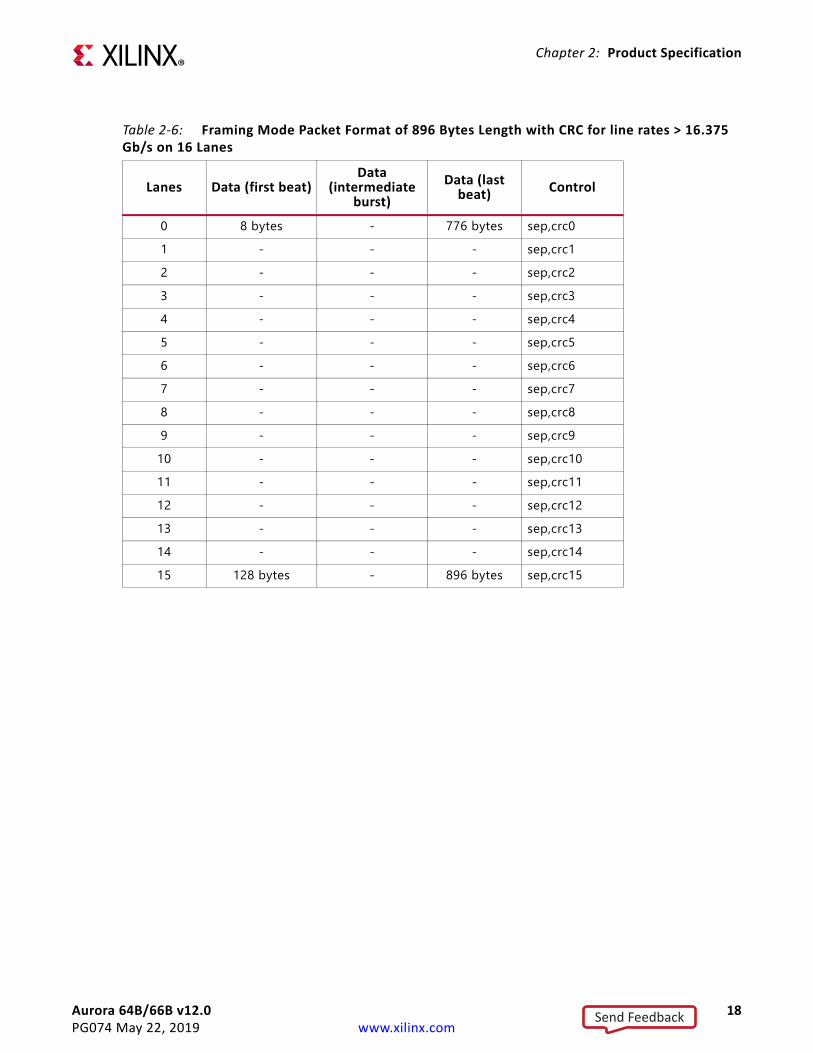
Data striping is handled differently for line-rates above 16.375Gb/s. See Table 2-6 for this packet format. Specifically, on the last cycle of a frame, all the lanes contain data blocks. Some of these blocks can be empty or be half full. On the next cycle, all the lanes transmit a SEP block, each one containing the number of valid bytes transmitted in the previous cycle in that lane. When using CRC, these SEP blocks also contain the 32-bit CRC for that lane over a duration of the recent frame.
Table 2-5: Typical Channel Frame
Data Byte 0 Data Byte 1 Data Byte 2 Data Byte 3 . . . Data Byte n–2
Data Byte n–1 Data Byte n
SEP (1E) Count (4) Data Byte 0
Data Byte 1
Data Byte 2
Data Byte 3
x x
Send Feedback
Aurora 64B/66B v12.0 18PG074 May 22, 2019 www.xilinx.com
Chapter 2: Product Specification
Table 2-6: Framing Mode Packet Format of 896 Bytes Length with CRC for line rates > 16.375 Gb/s on 16 Lanes
Lanes Data (first beat)Data
(intermediate burst)
Data (last beat) Control
0 8 bytes - 776 bytes sep,crc01 - - - sep,crc12 - - - sep,crc23 - - - sep,crc34 - - - sep,crc45 - - - sep,crc56 - - - sep,crc67 - - - sep,crc78 - - - sep,crc89 - - - sep,crc9
10 - - - sep,crc1011 - - - sep,crc1112 - - - sep,crc1213 - - - sep,crc1314 - - - sep,crc1415 128 bytes - 896 bytes sep,crc15
Send Feedback
Aurora 64B/66B v12.0 19PG074 May 22, 2019 www.xilinx.com
Chapter 2: Product Specification
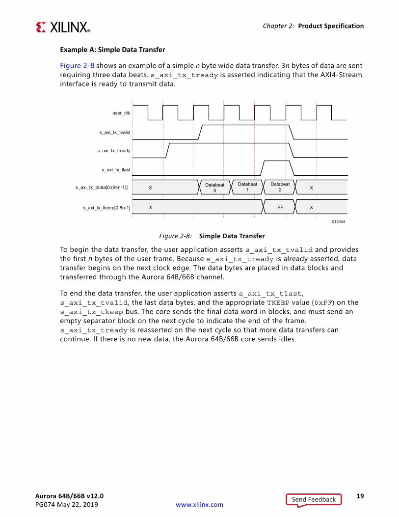
Example A: Simple Data Transfer
Figure 2-8 shows an example of a simple n byte wide data transfer. 3n bytes of data are sent requiring three data beats. s_axi_tx_tready is asserted indicating that the AXI4-Stream interface is ready to transmit data.
To begin the data transfer, the user application asserts s_axi_tx_tvalid and provides the first n bytes of the user frame. Because s_axi_tx_tready is already asserted, data transfer begins on the next clock edge. The data bytes are placed in data blocks and transferred through the Aurora 64B/66B channel.
To end the data transfer, the user application asserts s_axi_tx_tlast, s_axi_tx_tvalid, the last data bytes, and the appropriate TKEEP value (0xFF) on the s_axi_tx_tkeep bus. The core sends the final data word in blocks, and must send an empty separator block on the next cycle to indicate the end of the frame. s_axi_tx_tready is reasserted on the next cycle so that more data transfers can continue. If there is no new data, the Aurora 64B/66B core sends idles.
X-Ref Target - Figure 2-8
Figure 2-8: Simple Data Transfer
s_axi_tx_tvalid
s_axi_tx_tlast
s_axi_tx_tdata[0:(64n-1)]
user_clk
s_axi_tx_tkeep[0:8n-1]
X Databeat0
X FF X
X13044
Databeat 1
Databeat 2 X
s_axi_tx_tready
Send Feedback
Aurora 64B/66B v12.0 20PG074 May 22, 2019 www.xilinx.com
Chapter 2: Product Specification
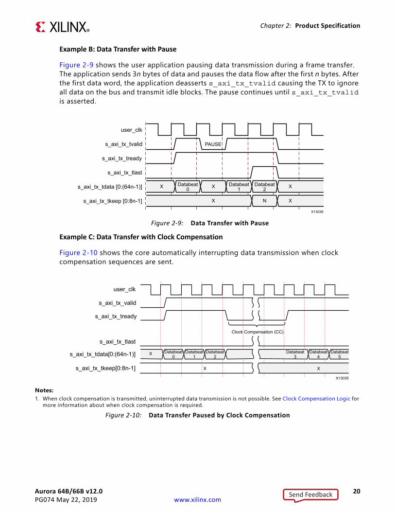
Example B: Data Transfer with Pause
Figure 2-9 shows the user application pausing data transmission during a frame transfer. The application sends 3n bytes of data and pauses the data flow after the first n bytes. After the first data word, the application deasserts s_axi_tx_tvalid causing the TX to ignore all data on the bus and transmit idle blocks. The pause continues until s_axi_tx_tvalid is asserted.
Example C: Data Transfer with Clock Compensation
Figure 2-10 shows the core automatically interrupting data transmission when clock compensation sequences are sent.
X-Ref Target - Figure 2-9
Figure 2-9: Data Transfer with Pause
user_clk
s_axi_tx_tvalid
s_axi_tx_tready
s_axi_tx_tlast
s_axi_tx_tdata [0:(64n-1)]
s_axi_tx_tkeep [0:8n-1]
X13036
PAUSE
Databeat0 X
X N X
XX Databeat2
Databeat1
X-Ref Target - Figure 2-10
Notes: 1. When clock compensation is transmitted, uninterrupted data transmission is not possible. See Clock Compensation Logic for
more information about when clock compensation is required.Figure 2-10: Data Transfer Paused by Clock Compensation
s_axi_tx_valid
s_axi_tx_tready
user_clk
X13035
s_axi_tx_tlast
Clock Compensation (CC)
Databeat 0
Databeat 1
Databeat 2
Databeat 4
Databeat 5
X
X
X
Databeat 3s_axi_tx_tdata[0:(64n-1)]
s_axi_tx_tkeep[0:8n-1]
Send Feedback
Aurora 64B/66B v12.0 21PG074 May 22, 2019 www.xilinx.com
Chapter 2: Product Specification
Receiving Data
Because the core has no built-in buffer for user data, there is no m_axi_rx_tready signal on the RX AXI4-Stream interface. User application control of the flow of data from an Aurora 64B/66B channel is limited to one of the optional core flow control features.
The m_axi_rx_tvalid signal is asserted concurrently with the first word of each frame from the core. The m_axi_rx_tlast signal is asserted concurrently with the last word or partial word of each frame. The m_axi_rx_tkeep port indicates the number of valid bytes in the final word of each frame using the same byte indication procedure as s_axi_tx_tkeep. All bytes valid is indicated (all 1s) when m_axi_rx_tlast is not asserted and the exact number of bytes valid is specified when m_axi_rx_tlast is asserted.
If the CRC option is selected, the received data stream is computed for the expected CRC value. The CRC block re-calculates the m_axi_rx_tkeep value and correspondingly asserts m_axi_rx_tlast.
The core can deassert m_axi_rx_tvalid anytime, even during a frame.
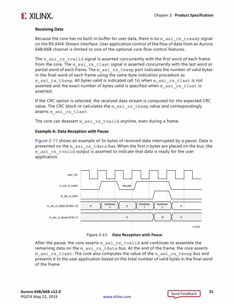
Example A: Data Reception with Pause
Figure 2-11 shows an example of 3n bytes of received data interrupted by a pause. Data is presented on the m_axi_rx_tdata bus. When the first n bytes are placed on the bus, the m_axi_rx_tvalid output is asserted to indicate that data is ready for the user application.
After the pause, the core asserts m_axi_rx_tvalid and continues to assemble the remaining data on the m_axi_rx_tdata bus. At the end of the frame, the core asserts m_axi_rx_tlast. The core also computes the value of the m_axi_rx_tkeep bus and presents it to the user application based on the total number of valid bytes in the final word of the frame.
X-Ref Target - Figure 2-11
Figure 2-11: Data Reception with Pause
m_axi_rx_tvalid
m_axi_rx_tlast
m_axi_rx_tdata [0:(64n-1)]
user_clk
m_axi_rx_tkeep [0:8n-1]
PAUSE
X X X
X N X
X13034
Databeat 0
Databeat 1
Databeat 2
Send Feedback
Aurora 64B/66B v12.0 22PG074 May 22, 2019 www.xilinx.com
Chapter 2: Product Specification
Framing Efficiency
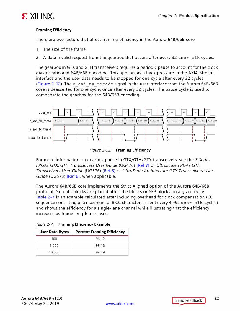
There are two factors that affect framing efficiency in the Aurora 64B/66B core:
1. The size of the frame.2. A data invalid request from the gearbox that occurs after every 32 user_clk cycles.
The gearbox in GTX and GTH transceivers requires a periodic pause to account for the clock divider ratio and 64B/66B encoding. This appears as a back pressure in the AXI4-Stream interface and the user data needs to be stopped for one cycle after every 32 cycles (Figure 2-12). The s_axi_tx_tready signal in the user interface from the Aurora 64B/66B core is deasserted for one cycle, once after every 32 cycles. The pause cycle is used to compensate the gearbox for the 64B/66B encoding.
For more information on gearbox pause in GTX/GTH/GTY transceivers, see the 7 Series FPGAs GTX/GTH Transceivers User Guide (UG476) [Ref 7] or UltraScale FPGAs GTH Transceivers User Guide (UG576) [Ref 5] or UltraScale Architecture GTY Transceivers User Guide (UG578) [Ref 6], when applicable.
The Aurora 64B/66B core implements the Strict Aligned option of the Aurora 64B/66B protocol. No data blocks are placed after idle blocks or SEP blocks on a given cycle. Table 2-7 is an example calculated after including overhead for clock compensation (CC sequence consisting of a maximum of 8 CC characters is sent every 4,992 user_clk cycles) and shows the efficiency for a single-lane channel while illustrating that the efficiency increases as frame length increases.
X-Ref Target - Figure 2-12
Figure 2-12: Framing Efficiency
user_clk
s_axi_tx_tdata
s_axi_tx_tvalid
s_axi_tx_tready
1 2 31 32 33 34 35 64 65 66 67
Databeat 0 Databeat 1 Databeat 30 Databeat 31 Invalid Data Databeat 32 Databeat 33 Databeat 62 Databeat 63 Invalid Data Databeat 64
Table 2-7: Framing Efficiency ExampleUser Data Bytes Percent Framing Efficiency
100 96.121,000 99.18
10,000 99.89
Send Feedback
Aurora 64B/66B v12.0 23PG074 May 22, 2019 www.xilinx.com
Chapter 2: Product Specification
Table 2-8 shows the overhead in a single-lane channel when transmitting 256 bytes of frame data. The resulting data unit is 264 bytes long due to the end-of-frame SEP block. This results in a 3.03% transmitter overhead. Also, the clock compensation blocks must be transmitted for at least three cycles every 10,000 cycles resulting in an additional 0.03% overhead in the transmitter.
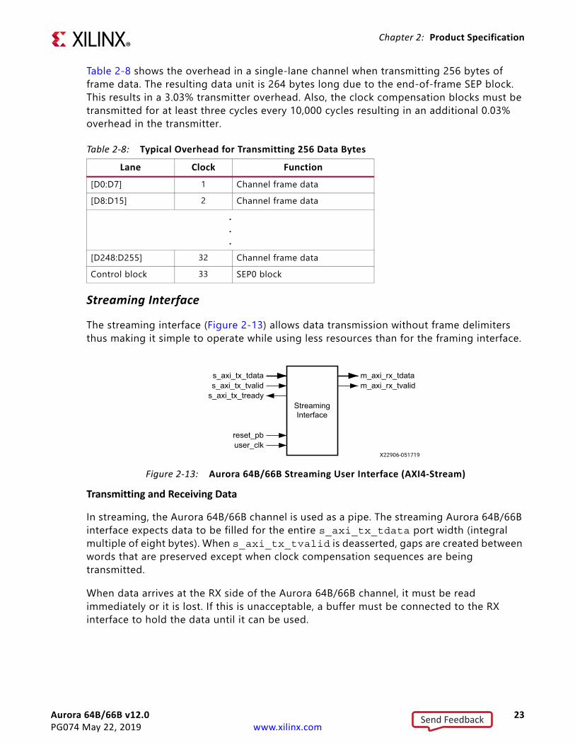
Streaming Interface
The streaming interface (Figure 2-13) allows data transmission without frame delimiters thus making it simple to operate while using less resources than for the framing interface.
Transmitting and Receiving Data
In streaming, the Aurora 64B/66B channel is used as a pipe. The streaming Aurora 64B/66B interface expects data to be filled for the entire s_axi_tx_tdata port width (integral multiple of eight bytes). When s_axi_tx_tvalid is deasserted, gaps are created between words that are preserved except when clock compensation sequences are being transmitted.
When data arrives at the RX side of the Aurora 64B/66B channel, it must be read immediately or it is lost. If this is unacceptable, a buffer must be connected to the RX interface to hold the data until it can be used.
Table 2-8: Typical Overhead for Transmitting 256 Data BytesLane Clock Function
[D0:D7] 1 Channel frame data[D8:D15] 2 Channel frame data
.
.
.[D248:D255] 32 Channel frame dataControl block 33 SEP0 block
X-Ref Target - Figure 2-13
Figure 2-13: Aurora 64B/66B Streaming User Interface (AXI4-Stream)
Streaming Interface
reset_pbuser_clk
s_axi_tx_tdatas_axi_tx_tvalid
s_axi_tx_tready
m_axi_rx_tdatam_axi_rx_tvalid
Send Feedback
Aurora 64B/66B v12.0 24PG074 May 22, 2019 www.xilinx.com
Chapter 2: Product Specification
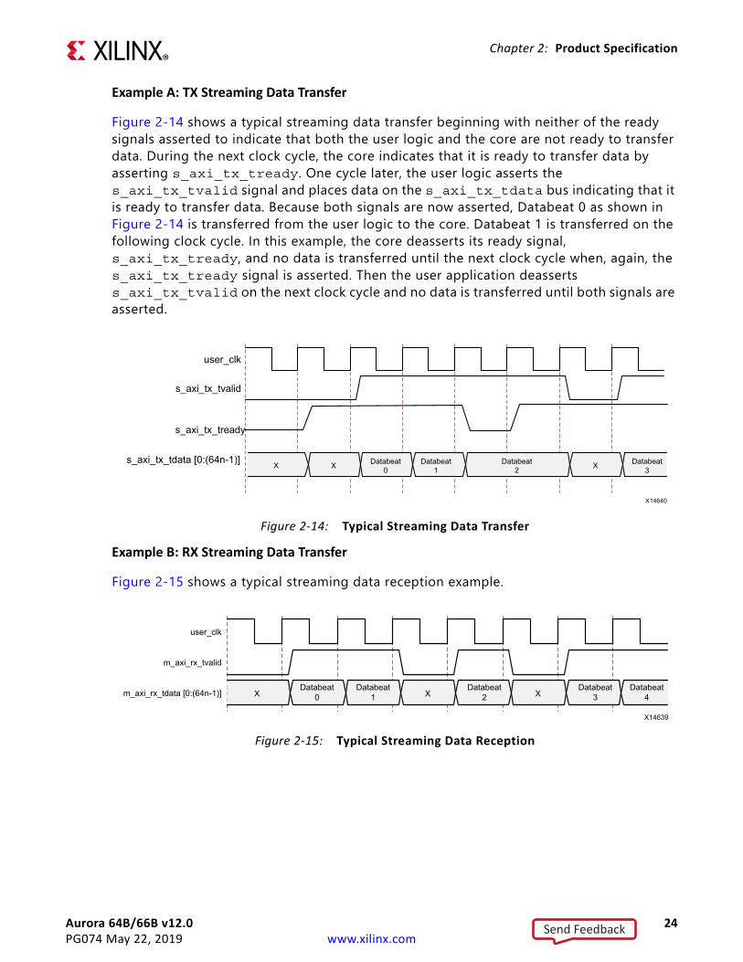
Example A: TX Streaming Data Transfer
Figure 2-14 shows a typical streaming data transfer beginning with neither of the ready signals asserted to indicate that both the user logic and the core are not ready to transfer data. During the next clock cycle, the core indicates that it is ready to transfer data by asserting s_axi_tx_tready. One cycle later, the user logic asserts the s_axi_tx_tvalid signal and places data on the s_axi_tx_tdata bus indicating that it is ready to transfer data. Because both signals are now asserted, Databeat 0 as shown in Figure 2-14 is transferred from the user logic to the core. Databeat 1 is transferred on the following clock cycle. In this example, the core deasserts its ready signal, s_axi_tx_tready, and no data is transferred until the next clock cycle when, again, the s_axi_tx_tready signal is asserted. Then the user application deasserts s_axi_tx_tvalid on the next clock cycle and no data is transferred until both signals are asserted.
Example B: RX Streaming Data Transfer
Figure 2-15 shows a typical streaming data reception example.
X-Ref Target - Figure 2-14
Figure 2-14: Typical Streaming Data Transfer
X-Ref Target - Figure 2-15
Figure 2-15: Typical Streaming Data Reception
user_clk
s_axi_tx_tvalid
s_axi_tx_tready
s_axi_tx_tdata [0:(64n-1)]X X XDatabeat
0Databeat
1Databeat
2
X14640
Databeat3
user_clk
m_axi_rx_tvalid
m_axi_rx_tdata [0:(64n-1)] X X XDatabeat
0Databeat
1Databeat
2Databeat
3Databeat
4
X14639
Send Feedback
Aurora 64B/66B v12.0 25PG074 May 22, 2019 www.xilinx.com
Chapter 2: Product Specification
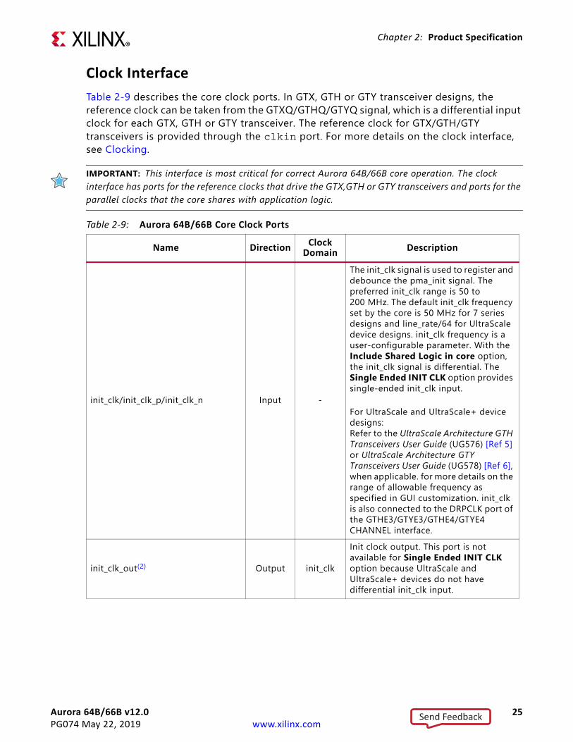
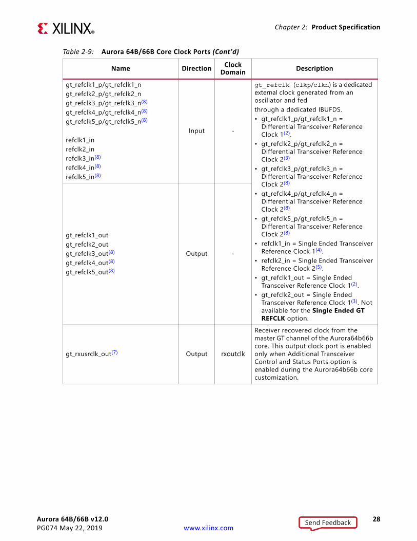
Clock InterfaceTable 2-9 describes the core clock ports. In GTX, GTH or GTY transceiver designs, the reference clock can be taken from the GTXQ/GTHQ/GTYQ signal, which is a differential input clock for each GTX, GTH or GTY transceiver. The reference clock for GTX/GTH/GTY transceivers is provided through the clkin port. For more details on the clock interface, see Clocking.
IMPORTANT: This interface is most critical for correct Aurora 64B/66B core operation. The clock interface has ports for the reference clocks that drive the GTX,GTH or GTY transceivers and ports for the parallel clocks that the core shares with application logic.
Table 2-9: Aurora 64B/66B Core Clock Ports
Name Direction Clock Domain Description
init_clk/init_clk_p/init_clk_n Input -
The init_clk signal is used to register and debounce the pma_init signal. The preferred init_clk range is 50 to 200 MHz. The default init_clk frequency set by the core is 50 MHz for 7 series designs and line_rate/64 for UltraScale device designs. init_clk frequency is a user-configurable parameter. With the Include Shared Logic in core option, the init_clk signal is differential. The Single Ended INIT CLK option provides single-ended init_clk input.
For UltraScale and UltraScale+ device designs:Refer to the UltraScale Architecture GTH Transceivers User Guide (UG576) [Ref 5] or UltraScale Architecture GTY Transceivers User Guide (UG578) [Ref 6], when applicable. for more details on the range of allowable frequency as specified in GUI customization. init_clk is also connected to the DRPCLK port of the GTHE3/GTYE3/GTHE4/GTYE4 CHANNEL interface.
init_clk_out(2) Output init_clk
Init clock output. This port is not available for Single Ended INIT CLK option because UltraScale and UltraScale+ devices do not have differential init_clk input.
Send Feedback
Aurora 64B/66B v12.0 26PG074 May 22, 2019 www.xilinx.com
Chapter 2: Product Specification
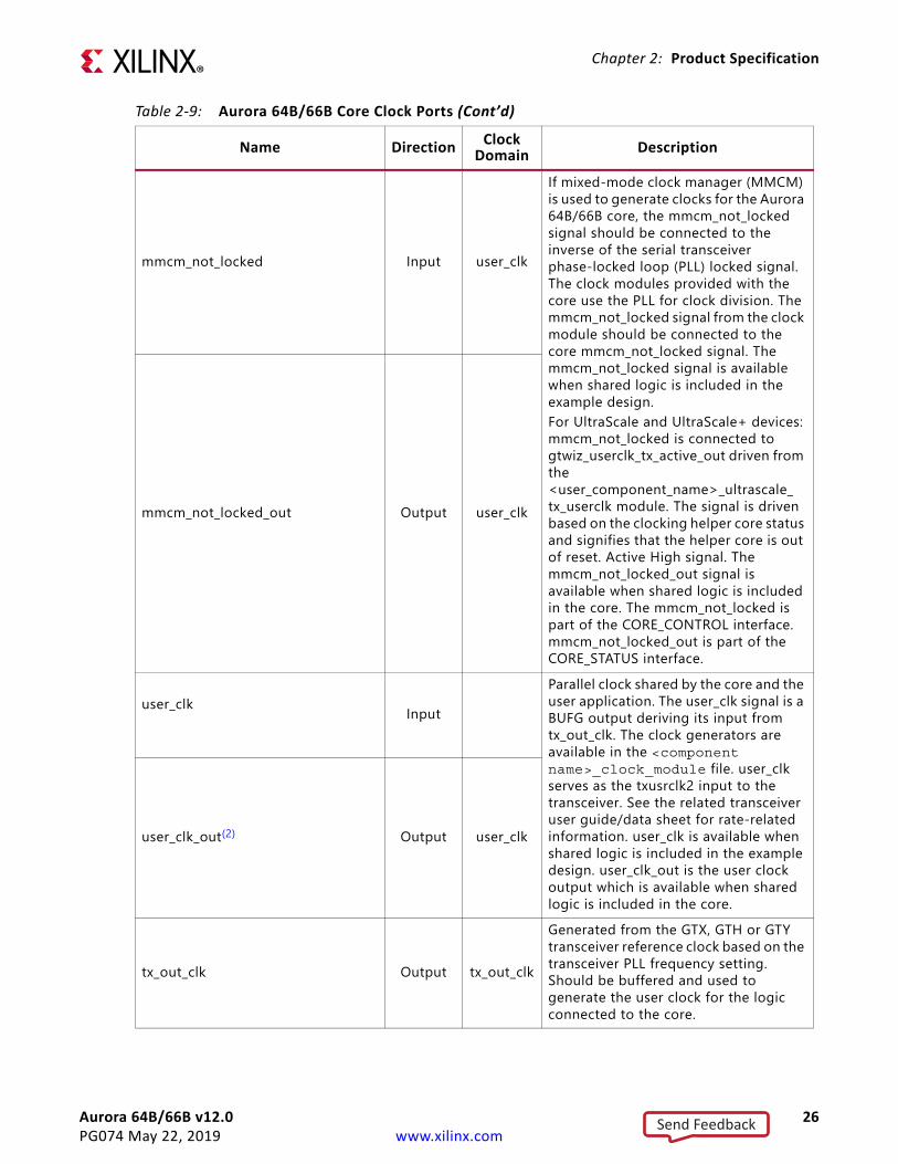
mmcm_not_locked Input user_clk
If mixed-mode clock manager (MMCM) is used to generate clocks for the Aurora 64B/66B core, the mmcm_not_locked signal should be connected to the inverse of the serial transceiver phase-locked loop (PLL) locked signal. The clock modules provided with the core use the PLL for clock division. The mmcm_not_locked signal from the clock module should be connected to the core mmcm_not_locked signal. The mmcm_not_locked signal is available when shared logic is included in the example design.For UltraScale and UltraScale+ devices:mmcm_not_locked is connected to gtwiz_userclk_tx_active_out driven from the <user_component_name>_ultrascale_tx_userclk module. The signal is driven based on the clocking helper core status and signifies that the helper core is out of reset. Active High signal. The mmcm_not_locked_out signal is available when shared logic is included in the core. The mmcm_not_locked is part of the CORE_CONTROL interface. mmcm_not_locked_out is part of the CORE_STATUS interface.
mmcm_not_locked_out Output user_clk
user_clk InputParallel clock shared by the core and the user application. The user_clk signal is a BUFG output deriving its input from tx_out_clk. The clock generators are available in the <component name>_clock_module file. user_clk serves as the txusrclk2 input to the transceiver. See the related transceiver user guide/data sheet for rate-related information. user_clk is available when shared logic is included in the example design. user_clk_out is the user clock output which is available when shared logic is included in the core.
user_clk_out(2) Output user_clk
tx_out_clk Output tx_out_clk
Generated from the GTX, GTH or GTY transceiver reference clock based on the transceiver PLL frequency setting. Should be buffered and used to generate the user clock for the logic connected to the core.
Table 2-9: Aurora 64B/66B Core Clock Ports (Cont’d)
Name Direction Clock Domain Description
Send Feedback
Aurora 64B/66B v12.0 27PG074 May 22, 2019 www.xilinx.com
Chapter 2: Product Specification
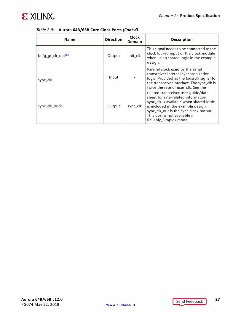
bufg_gt_clr_out(6) Output init_clkThis signal needs to be connected to the clock locked input of the clock module when using shared logic in the example design.
sync_clk Input -Parallel clock used by the serial transceiver internal synchronization logic. Provided as the txusrclk signal to the transceiver interface. The sync_clk is twice the rate of user_clk. See therelated transceiver user guide/data sheet for rate-related information. sync_clk is available when shared logic is included in the example design. sync_clk_out is the sync clock output. This port is not available in RX-only_Simplex mode.
sync_clk_out(2) Output sync_clk
Table 2-9: Aurora 64B/66B Core Clock Ports (Cont’d)
Name Direction Clock Domain Description
Send Feedback
Aurora 64B/66B v12.0 28PG074 May 22, 2019 www.xilinx.com
Chapter 2: Product Specification
gt_refclk1_p/gt_refclk1_ngt_refclk2_p/gt_refclk2_ngt_refclk3_p/gt_refclk3_n(8)
gt_refclk4_p/gt_refclk4_n(8)
gt_refclk5_p/gt_refclk5_n(8)
refclk1_inrefclk2_inrefclk3_in(8)
refclk4_in(8)
refclk5_in(8)
Input -
gt_refclk (clkp/clkn) is a dedicated external clock generated from an oscillator and fedthrough a dedicated IBUFDS.• gt_refclk1_p/gt_refclk1_n =
Differential Transceiver Reference Clock 1(2).
• gt_refclk2_p/gt_refclk2_n = Differential Transceiver Reference Clock 2(3)
• gt_refclk3_p/gt_refclk3_n = Differential Transceiver Reference Clock 2(8)
• gt_refclk4_p/gt_refclk4_n = Differential Transceiver Reference Clock 2(8)
• gt_refclk5_p/gt_refclk5_n = Differential Transceiver Reference Clock 2(8)
• refclk1_in = Single Ended Transceiver Reference Clock 1(4).
• refclk2_in = Single Ended Transceiver Reference Clock 2(5).
• gt_refclk1_out = Single Ended Transceiver Reference Clock 1(2).
• gt_refclk2_out = Single Ended Transceiver Reference Clock 1(3). Not available for the Single Ended GT REFCLK option.
gt_refclk1_outgt_refclk2_outgt_refclk3_out(8)
gt_refclk4_out(8)
gt_refclk5_out(8)
Output -
gt_rxusrclk_out(7) Output rxoutclk
Receiver recovered clock from the master GT channel of the Aurora64b66b core. This output clock port is enabled only when Additional Transceiver Control and Status Ports option is enabled during the Aurora64b66b core customization.
Table 2-9: Aurora 64B/66B Core Clock Ports (Cont’d)
Name Direction Clock Domain Description
Send Feedback
Aurora 64B/66B v12.0 29PG074 May 22, 2019 www.xilinx.com
Chapter 2: Product Specification
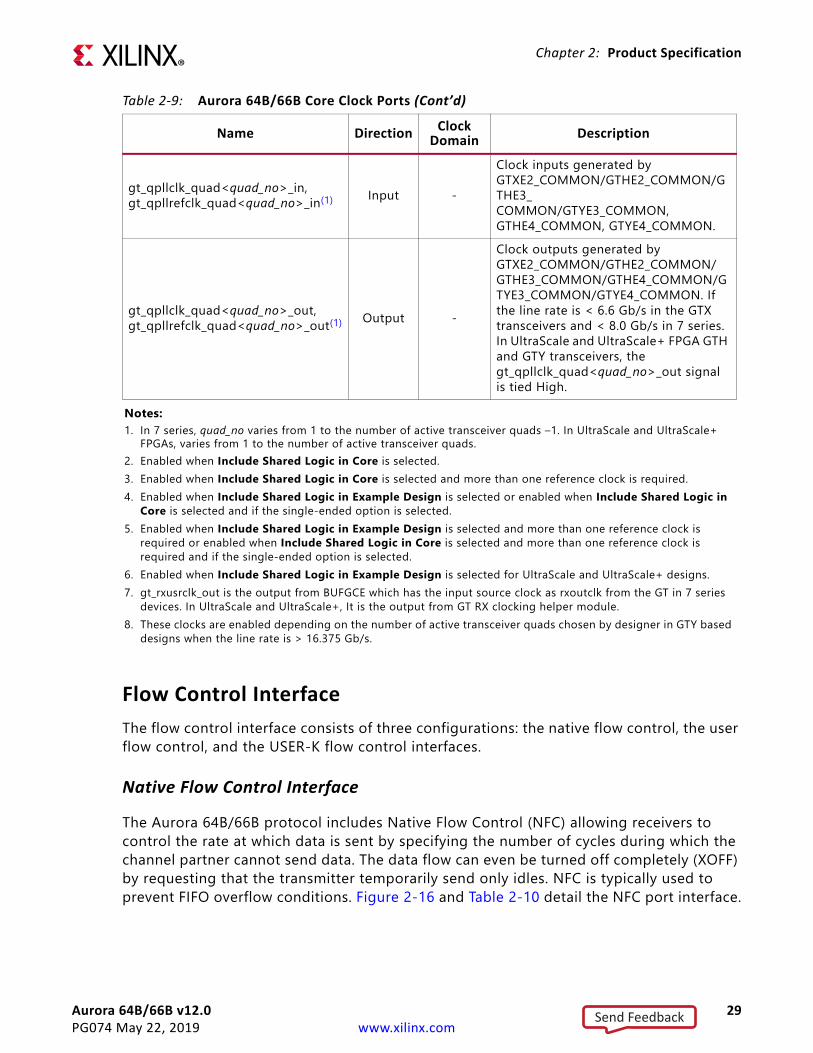
Flow Control InterfaceThe flow control interface consists of three configurations: the native flow control, the user flow control, and the USER-K flow control interfaces.
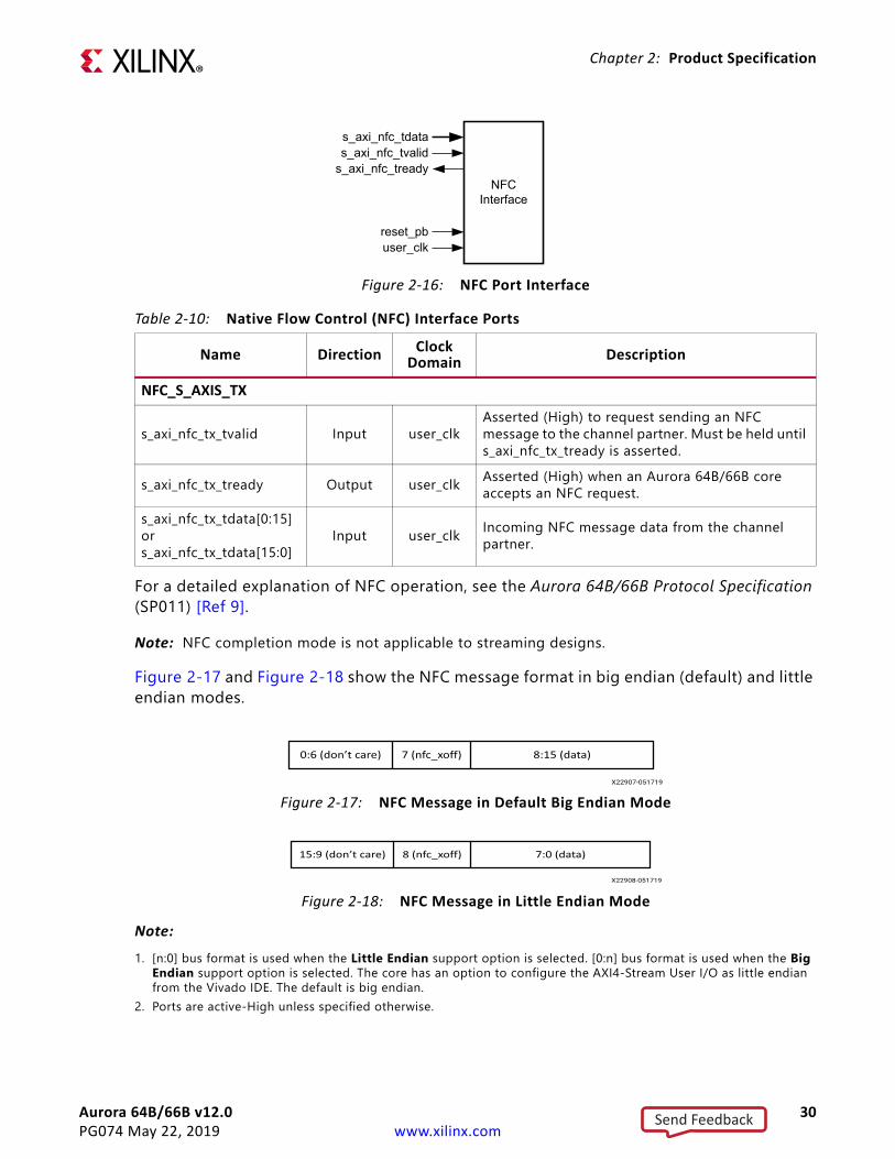
Native Flow Control Interface
The Aurora 64B/66B protocol includes Native Flow Control (NFC) allowing receivers to control the rate at which data is sent by specifying the number of cycles during which the channel partner cannot send data. The data flow can even be turned off completely (XOFF) by requesting that the transmitter temporarily send only idles. NFC is typically used to prevent FIFO overflow conditions. Figure 2-16 and Table 2-10 detail the NFC port interface.
gt_qpllclk_quad<quad_no>_in, gt_qpllrefclk_quad<quad_no>_in(1) Input -
Clock inputs generated by GTXE2_COMMON/GTHE2_COMMON/GTHE3_COMMON/GTYE3_COMMON, GTHE4_COMMON, GTYE4_COMMON.
gt_qpllclk_quad<quad_no>_out, gt_qpllrefclk_quad<quad_no>_out(1) Output -
Clock outputs generated by GTXE2_COMMON/GTHE2_COMMON/GTHE3_COMMON/GTHE4_COMMON/GTYE3_COMMON/GTYE4_COMMON. If the line rate is < 6.6 Gb/s in the GTX transceivers and < 8.0 Gb/s in 7 series. In UltraScale and UltraScale+ FPGA GTH and GTY transceivers, the gt_qpllclk_quad<quad_no>_out signal is tied High.
Notes: 1. In 7 series, quad_no varies from 1 to the number of active transceiver quads –1. In UltraScale and UltraScale+
FPGAs, varies from 1 to the number of active transceiver quads.2. Enabled when Include Shared Logic in Core is selected.3. Enabled when Include Shared Logic in Core is selected and more than one reference clock is required.4. Enabled when Include Shared Logic in Example Design is selected or enabled when Include Shared Logic in
Core is selected and if the single-ended option is selected.5. Enabled when Include Shared Logic in Example Design is selected and more than one reference clock is
required or enabled when Include Shared Logic in Core is selected and more than one reference clock is required and if the single-ended option is selected.
6. Enabled when Include Shared Logic in Example Design is selected for UltraScale and UltraScale+ designs.7. gt_rxusrclk_out is the output from BUFGCE which has the input source clock as rxoutclk from the GT in 7 series
devices. In UltraScale and UltraScale+, It is the output from GT RX clocking helper module.8. These clocks are enabled depending on the number of active transceiver quads chosen by designer in GTY based
designs when the line rate is > 16.375 Gb/s.
Table 2-9: Aurora 64B/66B Core Clock Ports (Cont’d)
Name Direction Clock Domain Description
Send Feedback
Aurora 64B/66B v12.0 30PG074 May 22, 2019 www.xilinx.com
Chapter 2: Product Specification
For a detailed explanation of NFC operation, see the Aurora 64B/66B Protocol Specification (SP011) [Ref 9].
Note: NFC completion mode is not applicable to streaming designs.
Figure 2-17 and Figure 2-18 show the NFC message format in big endian (default) and little endian modes.
Note:1. [n:0] bus format is used when the Little Endian support option is selected. [0:n] bus format is used when the Big
Endian support option is selected. The core has an option to configure the AXI4-Stream User I/O as little endian from the Vivado IDE. The default is big endian.
2. Ports are active-High unless specified otherwise.
X-Ref Target - Figure 2-16
Figure 2-16: NFC Port Interface
Table 2-10: Native Flow Control (NFC) Interface Ports
Name Direction Clock Domain Description
NFC_S_AXIS_TX
s_axi_nfc_tx_tvalid Input user_clkAsserted (High) to request sending an NFC message to the channel partner. Must be held until s_axi_nfc_tx_tready is asserted.
s_axi_nfc_tx_tready Output user_clk Asserted (High) when an Aurora 64B/66B core accepts an NFC request.
s_axi_nfc_tx_tdata[0:15] or s_axi_nfc_tx_tdata[15:0]
Input user_clk Incoming NFC message data from the channel partner.
X-Ref Target - Figure 2-17
Figure 2-17: NFC Message in Default Big Endian ModeX-Ref Target - Figure 2-18
Figure 2-18: NFC Message in Little Endian Mode
NFC Interface
reset_pbuser_clk
s_axi_nfc_tdatas_axi_nfc_tvalid
s_axi_nfc_tready
0:6 (don’t care) 7 (nfc_xoff) 8:15 (data)
15:9 (don’t care) 8 (nfc_xoff) 7:0 (data)
Send Feedback
Aurora 64B/66B v12.0 31PG074 May 22, 2019 www.xilinx.com
Chapter 2: Product Specification
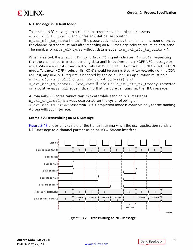
NFC Message in Default Mode
To send an NFC message to a channel partner, the user application asserts s_axi_nfc_tx_tvalid and writes an 8-bit pause count to s_axi_nfc_tx_tdata[8:15]. The pause code indicates the minimum number of cycles the channel partner must wait after receiving an NFC message prior to resuming data send. The number of user_clk cycles without data is equal to s_axi_nfc_tx_tdata + 1.
When asserted, the s_axi_nfc_tx_tdata[7] signal indicates nfc_xoff, requesting that the channel partner stop sending data until it receives a non-XOFF NFC message or reset. When a request is transmitted with PAUSE and XOFF both set to 0, NFC is set to XON mode. To cancel XOFF mode, all 0s (XON) should be transmitted. After reception of this XON request, any new NFC request is honored by the core. The user application must hold s_axi_nfc_tx_tvalid, s_axi_nfc_tx_tdata[8:15], and s_axi_nfc_tx_tdata[7] (nfc_xoff, if used) until s_axi_nfc_tx_tready is asserted on a positive user_clk edge indicating that the core can transmit the NFC message.
Aurora 64B/66B cores cannot transmit data while sending NFC messages. s_axi_tx_tready is always deasserted on the cycle following an s_axi_nfc_tx_tready assertion. NFC Completion mode is available only for the framing Aurora 64B/66B interface.
Example A: Transmitting an NFC Message
Figure 2-19 shows an example of the transmit timing when the user application sends an NFC message to a channel partner using an AXI4-Stream interface.X-Ref Target - Figure 2-19
Figure 2-19: Transmitting an NFC Message
user_clk
s_axi_tx_tkeep [0:8n-1]
s_axi_tx_tlast
s_axi_tx_tvalid
s_axi_tx_tready
s_axi_nfc_tx_tvalid
s_axi_nfc_tx_tready
s_axi_nfc_tx_tdata [0:15]
s_axi_tx_tdata [0:(64n-1)]
NFC sent
X
X
X
X X 4 X X X
X X X X X X
Databeat0
Databeat1
Databeat2
Databeat3
Databeat4
Databeat5
X14644
Send Feedback
Aurora 64B/66B v12.0 32PG074 May 22, 2019 www.xilinx.com
Chapter 2: Product Specification
Note: Signal s_axi_tx_tready is deasserted for one cycle to create the gap in the data flow in which the NFC message is placed.
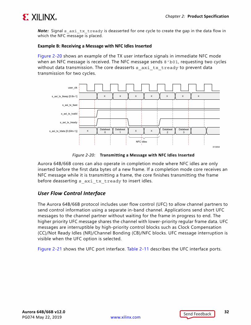
Example B: Receiving a Message with NFC Idles Inserted
Figure 2-20 shows an example of the TX user interface signals in immediate NFC mode when an NFC message is received. The NFC message sends 8'b01, requesting two cycles without data transmission. The core deasserts s_axi_tx_tready to prevent data transmission for two cycles.
Aurora 64B/66B cores can also operate in completion mode where NFC idles are only inserted before the first data bytes of a new frame. If a completion mode core receives an NFC message while it is transmitting a frame, the core finishes transmitting the frame before deasserting s_axi_tx_tready to insert idles.
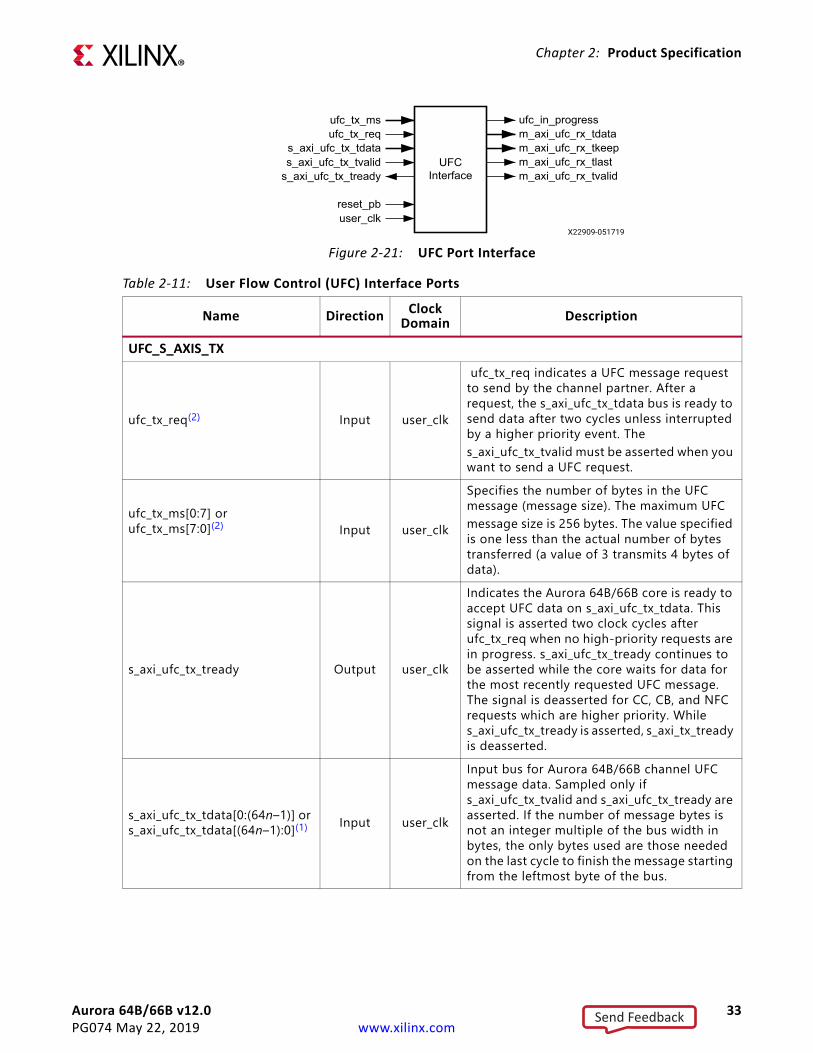
User Flow Control Interface
The Aurora 64B/66B protocol includes user flow control (UFC) to allow channel partners to send control information using a separate in-band channel. Applications send short UFC messages to the channel partner without waiting for the frame in progress to end. The higher priority UFC message shares the channel with lower-priority regular frame data. UFC messages are interruptible by high-priority control blocks such as Clock Compensation (CC)/Not Ready Idles (NR)/Channel Bonding (CB)/NFC blocks. UFC message interruption is visible when the UFC option is selected.
Figure 2-21 shows the UFC port interface. Table 2-11 describes the UFC interface ports.
X-Ref Target - Figure 2-20
Figure 2-20: Transmitting a Message with NFC Idles Inserted
X13054
user_clk
s_axi_tx_tkeep [0:8n-1]
s_axi_tx_tlast
s_axi_tx_tvalid
s_axi_tx_tready
s_axi_tx_tdata [0:(64n-1)]
NFC Idles
X
X X X
X X X X X X
Databeat0
Databeat1
Databeat2
Databeat3
Send Feedback
Aurora 64B/66B v12.0 33PG074 May 22, 2019 www.xilinx.com
Chapter 2: Product Specification
X-Ref Target - Figure 2-21
Figure 2-21: UFC Port Interface
Table 2-11: User Flow Control (UFC) Interface Ports
Name Direction Clock Domain Description
UFC_S_AXIS_TX
ufc_tx_req(2) Input user_clk
ufc_tx_req indicates a UFC message request to send by the channel partner. After a request, the s_axi_ufc_tx_tdata bus is ready to send data after two cycles unless interrupted by a higher priority event. Thes_axi_ufc_tx_tvalid must be asserted when you want to send a UFC request.
ufc_tx_ms[0:7] or ufc_tx_ms[7:0](2) Input user_clk
Specifies the number of bytes in the UFC message (message size). The maximum UFCmessage size is 256 bytes. The value specified is one less than the actual number of bytes transferred (a value of 3 transmits 4 bytes of data).
s_axi_ufc_tx_tready Output user_clk
Indicates the Aurora 64B/66B core is ready to accept UFC data on s_axi_ufc_tx_tdata. This signal is asserted two clock cycles after ufc_tx_req when no high-priority requests are in progress. s_axi_ufc_tx_tready continues to be asserted while the core waits for data for the most recently requested UFC message. The signal is deasserted for CC, CB, and NFC requests which are higher priority. While s_axi_ufc_tx_tready is asserted, s_axi_tx_tready is deasserted.
s_axi_ufc_tx_tdata[0:(64n–1)] or s_axi_ufc_tx_tdata[(64n–1):0](1) Input user_clk
Input bus for Aurora 64B/66B channel UFC message data. Sampled only if s_axi_ufc_tx_tvalid and s_axi_ufc_tx_tready are asserted. If the number of message bytes is not an integer multiple of the bus width in bytes, the only bytes used are those needed on the last cycle to finish the message starting from the leftmost byte of the bus.
UFC Interface
reset_pbuser_clk
s_axi_ufc_tx_tdata
ufc_tx_msufc_tx_req
s_axi_ufc_tx_tvalids_axi_ufc_tx_tready
m_axi_ufc_rx_tdatam_axi_ufc_rx_tkeepm_axi_ufc_rx_tlastm_axi_ufc_rx_tvalid
ufc_in_progress
Send Feedback
Aurora 64B/66B v12.0 34PG074 May 22, 2019 www.xilinx.com
Chapter 2: Product Specification
Transmitting UFC Messages
To send a UFC message, the application asserts ufc_tx_req while driving ufc_tx_ms with the desired SIZE code for a single cycle. After a request, a new request cannot be made until s_axi_ufc_tx_tready is asserted for the final cycle of the previous request. The UFC message data must be placed on s_axi_ufc_tx_tdata and the s_axi_ufc_tx_tvalid signal must be asserted whenever the bus contains valid message data.
The core deasserts s_axi_tx_tready while sending UFC data and keeps s_axi_ufc_tx_tready asserted until it has enough data to complete the requested message. If s_axi_ufc_tx_tvalid is deasserted during a UFC message, idles are sent, s_axi_tx_tready remains deasserted, and s_axi_ufc_tx_tready remains asserted. If a CC, CB, or NFC request is made, s_axi_ufc_tx_tready is deasserted while the requested operation is performed because CC, CB, and NFC requests have higher priority.
s_axi_ufc_tx_tvalid Input user_clkIndicates valid UFC data on s_axi_ufc_tx_tdata. If deasserted while s_axi_ufc_tx_tready is asserted, Idle blocks are sent in the UFC message.
UFC_M_AXIS_RXm_axi_ufc_rx_tdata[0:(64n–1)] or m_axi_ufc_rx_tdata[(64n–1):0](1)
Output user_clk Incoming UFC message data from the channel partner.
m_axi_ufc_rx_tvalid Output user_clkIndicates valid UFC data on the m_axi_ufc_rx_tdata port. When not asserted, all values on the m_axi_ufc_rx_tdata port should be ignored.
m_axi_ufc_rx_tlast Output user_clk Indicates the end of the incoming UFC message.
m_axi_ufc_rx_tkeep[0:(8n–1)] or m_axi_ufc_rx_tkeep[(8n–1):0](1) Output user_clk
Specifies the number of valid data bytes presented on the m_axi_ufc_rx_tdata port on the last word of a UFC message. Valid only when m_axi_ufc_rx_tlast is asserted. Each bit indicates one valid byte. Maximum size of the UFC message is 256 bytes.
ufc_in_progress(3) Output user_clkSpecifies the status of the current UFC transmission. This is an active-Low signal. A Low on this port indicates that UFC reception is in progress.
Notes: 1. n is the number of lanes.2. ufc_tx_req and ufc_tx_ms are available just below the UFC_S_AXIS_TX interface.3. ufc_in_progres is available just below the UFC_M_AXIS_RX interface.
Table 2-11: User Flow Control (UFC) Interface Ports (Cont’d)
Name Direction Clock Domain Description
Send Feedback
Aurora 64B/66B v12.0 35PG074 May 22, 2019 www.xilinx.com
Chapter 2: Product Specification
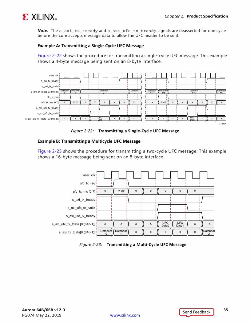
Note: The s_axi_tx_tready and s_axi_ufc_tx_tready signals are deasserted for one cycle before the core accepts message data to allow the UFC header to be sent.
Example A: Transmitting a Single-Cycle UFC Message
Figure 2-22 shows the procedure for transmitting a single-cycle UFC message. This example shows a 4-byte message being sent on an 8-byte interface.
Example B: Transmitting a Multicycle UFC Message
Figure 2-23 shows the procedure for transmitting a two-cycle UFC message. This example shows a 16-byte message being sent on an 8-byte interface.
X-Ref Target - Figure 2-22
Figure 2-22: Transmitting a Single-Cycle UFC Message
user_clk
s_axi_tx_tready
s_axi_tx_tvalid
s_axi_tx_tdata[0:(64n-1)]
ufc_tx_req
ufc_tx_ms [0:7]
s_axi_ufc_tx_tready
s_axi_ufc_tx_tvalid
s_axi_ufc_tx_tdata [0:(64n-1)]
Databeat0
Databeat1
Databeat2
Databeat3
Databeatn+4
Databeatn+5
Databeat n+6
Databeat n+7
X 8'h03 X X X X X X X 8'h03 X X X X X X
X X X X X X X X X X X X XUFCData
UFCData
X14636
X-Ref Target - Figure 2-23
Figure 2-23: Transmitting a Multi-Cycle UFC Message
user_clk
ufc_tx_req
ufc_tx_ms [0:7]
s_axi_tx_tready
s_axi_ufc_tx_tvalid
s_axi_ufc_tx_tready
s_axi_ufc_tx_tdata [0:(64n-1)]
s_axi_tx_tdata[0:(64n-1)]
X 8'h0F X X X X X
X X X X UFCData0
UFCData1 X X
Databeat0
Databeat1 X X X X X Databeat
2
Send Feedback
Aurora 64B/66B v12.0 36PG074 May 22, 2019 www.xilinx.com
Chapter 2: Product Specification
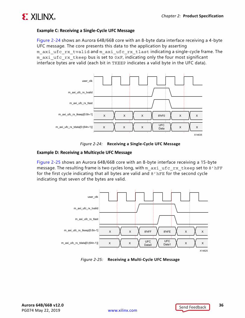
Example C: Receiving a Single-Cycle UFC Message
Figure 2-24 shows an Aurora 64B/66B core with an 8-byte data interface receiving a 4-byte UFC message. The core presents this data to the application by asserting m_axi_ufc_rx_tvalid and m_axi_ufc_rx_tlast indicating a single-cycle frame. The m_axi_ufc_rx_tkeep bus is set to 0xF, indicating only the four most significant interface bytes are valid (each bit in TKEEP indicates a valid byte in the UFC data).
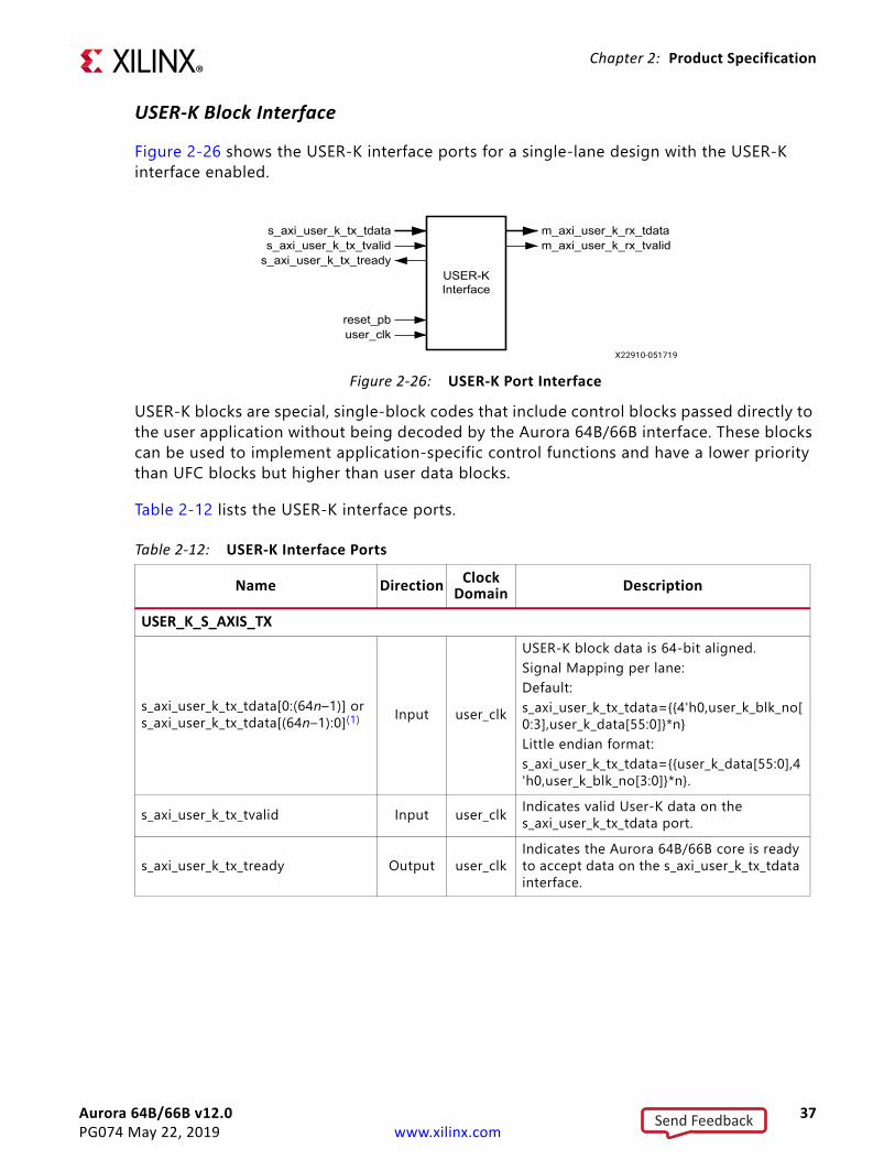
Example D: Receiving a Multicycle UFC Message
Figure 2-25 shows an Aurora 64B/66B core with an 8-byte interface receiving a 15-byte message. The resulting frame is two cycles long, with m_axi_ufc_rx_tkeep set to 8’hFF for the first cycle indicating that all bytes are valid and 8’hFE for the second cycle indicating that seven of the bytes are valid.
X-Ref Target - Figure 2-24
Figure 2-24: Receiving a Single-Cycle UFC Message
X-Ref Target - Figure 2-25
Figure 2-25: Receiving a Multi-Cycle UFC Message
m_axi_ufc_rx_tvalid
m_axi_ufc_rx_tkeep[0:8n-1]
m_axi_ufc_rx_tdata[0:(64n-1)]
user_clk
X
X14635
UFCData X
m_axi_ufc_rx_tlast
X XX 8'hF0
XX
X X
X
m_axi_ufc_rx_tvalid
m_axi_ufc_rx_tkeep[0:8n-1]
m_axi_ufc_rx_tdata[0:(64n-1)]
user_clk
UFCData0
X14625
UFCData1 X
m_axi_ufc_rx_tlast
X 8'hFFX 8'hFE
XX
X X
X
Send Feedback
Aurora 64B/66B v12.0 37PG074 May 22, 2019 www.xilinx.com
Chapter 2: Product Specification
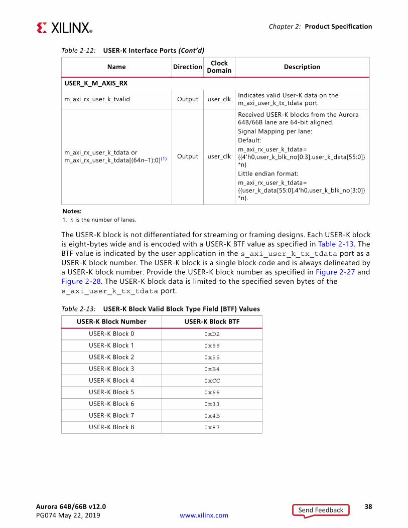
USER-K Block Interface
Figure 2-26 shows the USER-K interface ports for a single-lane design with the USER-K interface enabled.
USER-K blocks are special, single-block codes that include control blocks passed directly to the user application without being decoded by the Aurora 64B/66B interface. These blocks can be used to implement application-specific control functions and have a lower priority than UFC blocks but higher than user data blocks.
Table 2-12 lists the USER-K interface ports.
X-Ref Target - Figure 2-26
Figure 2-26: USER-K Port Interface
Table 2-12: USER-K Interface Ports
Name Direction Clock Domain Description
USER_K_S_AXIS_TX
s_axi_user_k_tx_tdata[0:(64n–1)] or s_axi_user_k_tx_tdata[(64n–1):0](1) Input user_clk
USER-K block data is 64-bit aligned.Signal Mapping per lane:Default:s_axi_user_k_tx_tdata={{4'h0,user_k_blk_no[0:3],user_k_data[55:0]}*n}Little endian format:s_axi_user_k_tx_tdata={{user_k_data[55:0],4'h0,user_k_blk_no[3:0]}*n}.
s_axi_user_k_tx_tvalid Input user_clk Indicates valid User-K data on the s_axi_user_k_tx_tdata port.
s_axi_user_k_tx_tready Output user_clkIndicates the Aurora 64B/66B core is ready to accept data on the s_axi_user_k_tx_tdata interface.
USER-K Interface
reset_pbuser_clk
s_axi_user_k_tx_tdatas_axi_user_k_tx_tvalid
s_axi_user_k_tx_tready
m_axi_user_k_rx_tdatam_axi_user_k_rx_tvalid
Send Feedback
Aurora 64B/66B v12.0 38PG074 May 22, 2019 www.xilinx.com
Chapter 2: Product Specification
The USER-K block is not differentiated for streaming or framing designs. Each USER-K block is eight-bytes wide and is encoded with a USER-K BTF value as specified in Table 2-13. The BTF value is indicated by the user application in the s_axi_user_k_tx_tdata port as a USER-K block number. The USER-K block is a single block code and is always delineated by a USER-K block number. Provide the USER-K block number as specified in Figure 2-27 and Figure 2-28. The USER-K block data is limited to the specified seven bytes of the s_axi_user_k_tx_tdata port.
USER_K_M_AXIS_RX
m_axi_rx_user_k_tvalid Output user_clk Indicates valid User-K data on the m_axi_user_k_tx_tdata port.
m_axi_rx_user_k_tdata or m_axi_rx_user_k_tdata[(64n–1):0](1) Output user_clk
Received USER-K blocks from the Aurora 64B/66B lane are 64-bit aligned.Signal Mapping per lane:Default:m_axi_rx_user_k_tdata={{4'h0,user_k_blk_no[0:3],user_k_data[55:0]}*n}Little endian format:m_axi_rx_user_k_tdata={{user_k_data[55:0],4'h0,user_k_blk_no[3:0]}*n}.
Notes: 1. n is the number of lanes.
Table 2-13: USER-K Block Valid Block Type Field (BTF) ValuesUSER-K Block Number USER-K Block BTF
USER-K Block 0 0xD2
USER-K Block 1 0x99
USER-K Block 2 0x55
USER-K Block 3 0xB4
USER-K Block 4 0xCC
USER-K Block 5 0x66
USER-K Block 6 0x33
USER-K Block 7 0x4B
USER-K Block 8 0x87
Table 2-12: USER-K Interface Ports (Cont’d)
Name Direction Clock Domain Description
Send Feedback
Aurora 64B/66B v12.0 39PG074 May 22, 2019 www.xilinx.com
Chapter 2: Product Specification
Figure 2-27 shows the USER-K format in default (big-endian) mode.
Figure 2-28 shows the USER-K format in little-endian mode.
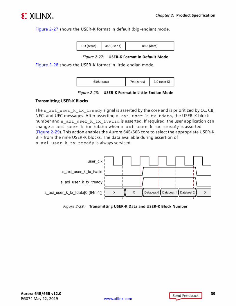
Transmitting USER-K Blocks
The s_axi_user_k_tx_tready signal is asserted by the core and is prioritized by CC, CB, NFC, and UFC messages. After asserting s_axi_user_k_tx_tdata, the USER-K block number and s_axi_user_k_tx_tvalid is asserted. If required, the user application can change s_axi_user_k_tx_tdata when s_axi_user_k_tx_tready is asserted (Figure 2-29). This action enables the Aurora 64B/66B core to select the appropriate USER-K BTF from the nine USER-K blocks. The data available during assertion of s_axi_user_k_tx_tready is always serviced.
X-Ref Target - Figure 2-27
Figure 2-27: USER-K Format in Default Mode
X-Ref Target - Figure 2-28
Figure 2-28: USER-K Format in Little-Endian Mode
X-Ref Target - Figure 2-29
Figure 2-29: Transmitting USER-K Data and USER-K Block Number
0:3 (zeros) 4:7 (user K) 8:63 (data)
7:4 (zeros) 3:0 (user K)63:8 (data)
user_clk
s_axi_user_k_tx_tvalid
s_axi_user_k_tx_tready
s_axi_user_k_tx_tdata[0:(64n-1)] X X Databeat 0 Databeat 1 Databeat 2 X
Send Feedback
Aurora 64B/66B v12.0 40PG074 May 22, 2019 www.xilinx.com
Chapter 2: Product Specification
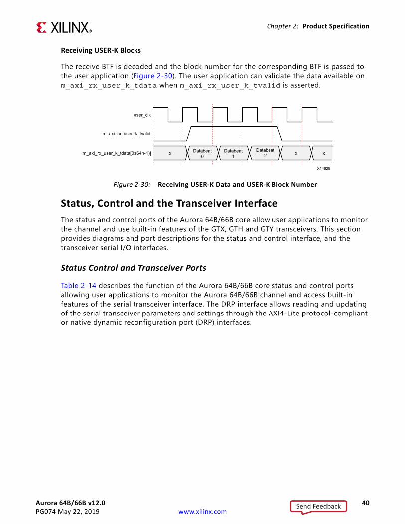
Receiving USER-K Blocks
The receive BTF is decoded and the block number for the corresponding BTF is passed to the user application (Figure 2-30). The user application can validate the data available on m_axi_rx_user_k_tdata when m_axi_rx_user_k_tvalid is asserted.
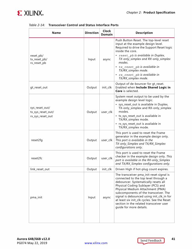
Status, Control and the Transceiver InterfaceThe status and control ports of the Aurora 64B/66B core allow user applications to monitor the channel and use built-in features of the GTX, GTH and GTY transceivers. This section provides diagrams and port descriptions for the status and control interface, and the transceiver serial I/O interfaces.
Status Control and Transceiver Ports
Table 2-14 describes the function of the Aurora 64B/66B core status and control ports allowing user applications to monitor the Aurora 64B/66B channel and access built-in features of the serial transceiver interface. The DRP interface allows reading and updating of the serial transceiver parameters and settings through the AXI4-Lite protocol-compliant or native dynamic reconfiguration port (DRP) interfaces.
X-Ref Target - Figure 2-30
Figure 2-30: Receiving USER-K Data and USER-K Block Number
m_axi_rx_user_k_tvalid
m_axi_rx_user_k_tdata[0:(64n-1)]
user_clk
Databeat 1
X14629
Databeat 2 XXX Databeat
0
Send Feedback
Aurora 64B/66B v12.0 41PG074 May 22, 2019 www.xilinx.com
Chapter 2: Product Specification
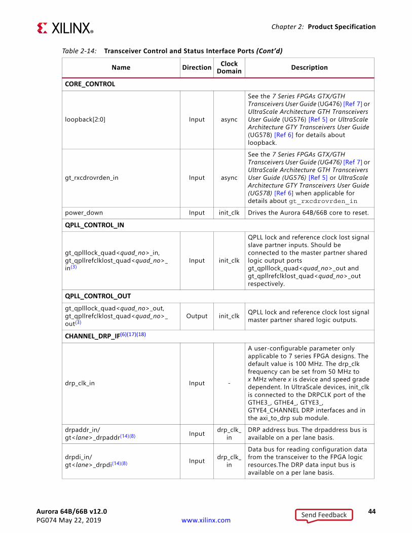
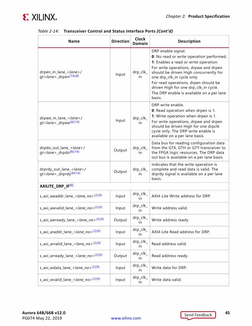
Table 2-14: Transceiver Control and Status Interface Ports
Name Direction Clock Domain Description
reset_pb/tx_reset_pb/rx_reset_pb
Input async
Push Button Reset. The top-level reset input at the example design level. Required to drive the Support Reset logic inside the core.• reset_pb is available in Duplex,
TX-only_simplex and RX-only_simplex modes.
• tx_reset_pb is available in TX/RX_simplex mode.
• rx_reset_pb is available in TX/RX_simplex mode.
gt_reset_out Output init_clkOutput of de-bouncer for gt_reset. Enabled when Include Shared Logic in Core is selected.
sys_reset_out/tx_sys_reset_out/rx_sys_reset_out
Output user_clk
System reset output to be used by the example design level logic.• sys_reset_out is available in Duplex,
TX-only_simplex and RX-only_simplex modes.
• tx_sys_reset_out is available in TX/RX_simplex mode.
• rx_sys_reset_out is available in TX/RX_simplex mode.
reset2fg Output user_clk
This port is used to reset the Frame generator in the example design only. This port is available in the TX-only_Simplex and TX/RX_Simplex configurations only.
reset2fc Output user_clkThis port is used to reset the Frame checker in the example design only. This port is available in the RX-only_Simplex and TX/RX_Simplex configurations only.
link_reset_out Output init_clk Driven High if hot-plug count expires.
pma_init Input async
The transceiver pma_init reset signal is connected to the top level through a debouncer. Systematically resets all Physical Coding Sublayer (PCS) and Physical Medium Attachment (PMA) subcomponents of the transceiver. The signal is debounced using init_clk_in for at least six init_clk cycles. See the Reset section in the related transceiver user guide for more details.
Send Feedback
Aurora 64B/66B v12.0 42PG074 May 22, 2019 www.xilinx.com
Chapter 2: Product Specification
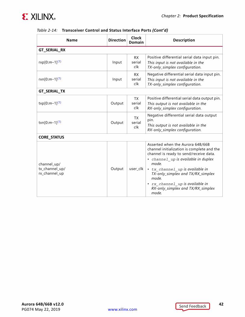
GT_SERIAL_RX
rxp[0:m–1](1) InputRX
serial clk
Positive differential serial data input pin.This input is not available in the TX-only_simplex configuration.
rxn[0:m–1](1) InputRX
serial clk
Negative differential serial data input pin.This input is not available in the TX-only_simplex configuration.
GT_SERIAL_TX
txp[0:m–1](1) OutputTX
serial clk
Positive differential serial data output pin.This output is not available in the RX-only_simplex configuration.
txn[0:m–1](1) OutputTX
serial clk
Negative differential serial data output pin.This output is not available in the RX-only_simplex configuration.
CORE_STATUS
channel_up/tx_channel_up/rx_channel_up
Output user_clk
Asserted when the Aurora 64B/66B channel initialization is complete and the channel is ready to send/receive data.• channel_up is available in duplex
mode.• tx_channel_up is available in
TX-only_simplex and TX/RX_simplex mode.
• rx_channel_up is available in RX-only_simplex and TX/RX_simplex mode.
Table 2-14: Transceiver Control and Status Interface Ports (Cont’d)
Name Direction Clock Domain Description
Send Feedback
Aurora 64B/66B v12.0 43PG074 May 22, 2019 www.xilinx.com
Chapter 2: Product Specification
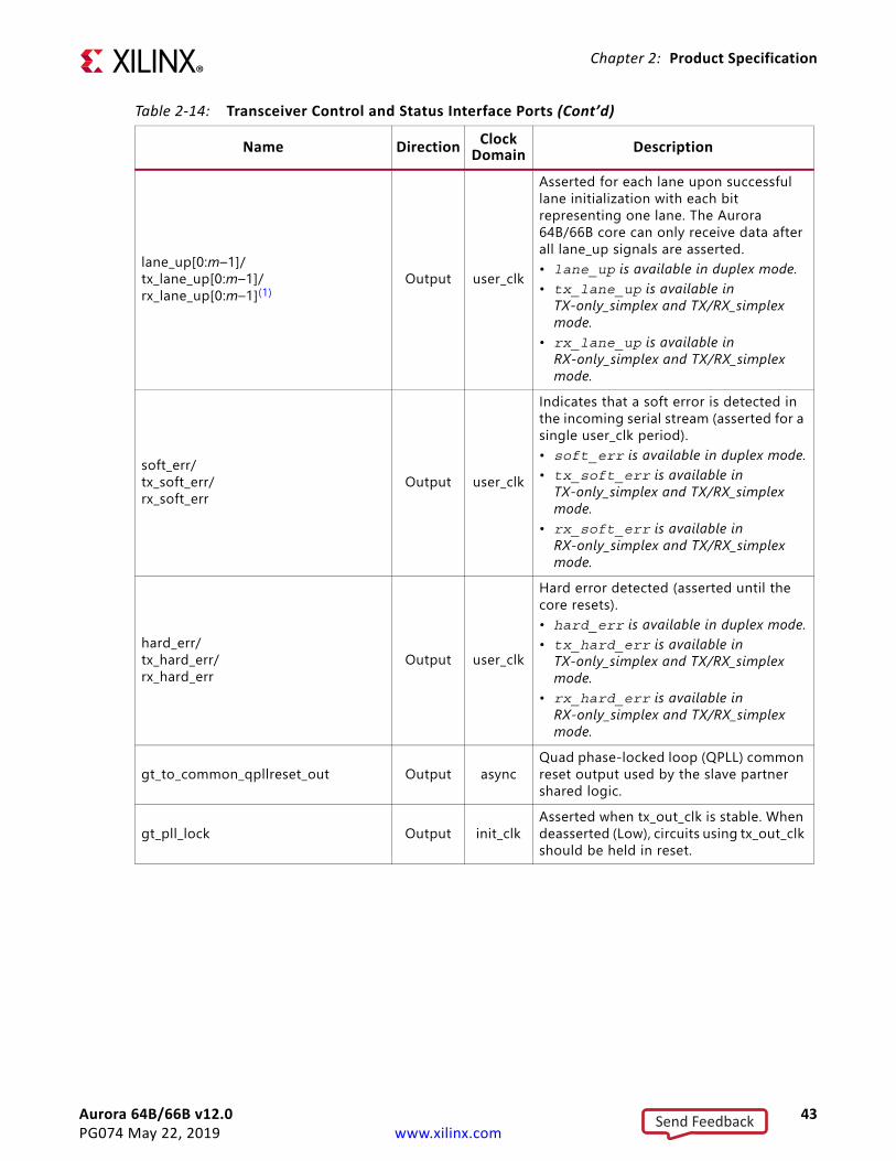
lane_up[0:m–1]/tx_lane_up[0:m–1]/rx_lane_up[0:m–1](1)
Output user_clk
Asserted for each lane upon successful lane initialization with each bit representing one lane. The Aurora 64B/66B core can only receive data after all lane_up signals are asserted.• lane_up is available in duplex mode.• tx_lane_up is available in
TX-only_simplex and TX/RX_simplex mode.
• rx_lane_up is available in RX-only_simplex and TX/RX_simplex mode.
soft_err/tx_soft_err/rx_soft_err
Output user_clk
Indicates that a soft error is detected in the incoming serial stream (asserted for a single user_clk period).• soft_err is available in duplex mode.• tx_soft_err is available in
TX-only_simplex and TX/RX_simplex mode.
• rx_soft_err is available in RX-only_simplex and TX/RX_simplex mode.
hard_err/tx_hard_err/rx_hard_err
Output user_clk
Hard error detected (asserted until the core resets).• hard_err is available in duplex mode.• tx_hard_err is available in
TX-only_simplex and TX/RX_simplex mode.
• rx_hard_err is available in RX-only_simplex and TX/RX_simplex mode.
gt_to_common_qpllreset_out Output asyncQuad phase-locked loop (QPLL) common reset output used by the slave partner shared logic.
gt_pll_lock Output init_clkAsserted when tx_out_clk is stable. When deasserted (Low), circuits using tx_out_clk should be held in reset.
Table 2-14: Transceiver Control and Status Interface Ports (Cont’d)
Name Direction Clock Domain Description
Send Feedback
Aurora 64B/66B v12.0 44PG074 May 22, 2019 www.xilinx.com
Chapter 2: Product Specification
CORE_CONTROL
loopback[2:0] Input async
See the 7 Series FPGAs GTX/GTH Transceivers User Guide (UG476) [Ref 7] or UltraScale Architecture GTH Transceivers User Guide (UG576) [Ref 5] or UltraScale Architecture GTY Transceivers User Guide (UG578) [Ref 6] for details about loopback.
gt_rxcdrovrden_in Input async
See the 7 Series FPGAs GTX/GTH Transceivers User Guide (UG476) [Ref 7] or UltraScale Architecture GTH Transceivers User Guide (UG576) [Ref 5] or UltraScale Architecture GTY Transceivers User Guide (UG578) [Ref 6] when applicable for details about gt_rxcdrovrden_in
power_down Input init_clk Drives the Aurora 64B/66B core to reset.QPLL_CONTROL_IN
gt_qplllock_quad<quad_no>_in, gt_qpllrefclklost_quad<quad_no>_in(3)
Input init_clk
QPLL lock and reference clock lost signal slave partner inputs. Should be connected to the master partner shared logic output ports gt_qplllock_quad<quad_no>_out and gt_qpllrefclklost_quad<quad_no>_out respectively.
QPLL_CONTROL_OUTgt_qplllock_quad<quad_no>_out, gt_qpllrefclklost_quad<quad_no>_out(3)
Output init_clk QPLL lock and reference clock lost signal master partner shared logic outputs.
CHANNEL_DRP_IF(6)(17)(18)
drp_clk_in Input -
A user-configurable parameter only applicable to 7 series FPGA designs. The default value is 100 MHz. The drp_clk frequency can be set from 50 MHz to x MHz where x is device and speed grade dependent. In UltraScale devices, init_clk is connected to the DRPCLK port of the GTHE3_, GTHE4_, GTYE3_, GTYE4_CHANNEL DRP interfaces and in the axi_to_drp sub module.
drpaddr_in/gt<lane>_drpaddr(14)(8) Input drp_clk_
inDRP address bus. The drpaddress bus is available on a per lane basis.
drpdi_in/gt<lane>_drpdi(14)(8) Input drp_clk_
in
Data bus for reading configuration data from the transceiver to the FPGA logic resources.The DRP data input bus is available on a per lane basis.
Table 2-14: Transceiver Control and Status Interface Ports (Cont’d)
Name Direction Clock Domain Description
Send Feedback
Aurora 64B/66B v12.0 45PG074 May 22, 2019 www.xilinx.com
Chapter 2: Product Specification
drpen_in_lane_<lane>/gt<lane>_drpen(14)(8) Input drp_clk_
in
DRP enable signal.0: No read or write operation performed.1: Enables a read or write operation.For write operations, drpwe and drpen should be driven High concurrently for one drp_clk_in cycle only.For read operations, drpen should be driven High for one drp_clk_in cycle.The DRP enable is available on a per lane basis.
drpwe_in_lane_<lane>/gt<lane>_drpwe(8)(14) Input drp_clk_
in
DRP write enable.0: Read operation when drpen is 1.1: Write operation when drpen is 1.For write operations, drpwe and drpen should be driven High for one drpclk cycle only. The DRP write enable is available on a per lane basis.
drpdo_out_lane_<lane>/gt<lane>_drpdo(8)(14) Output drp_clk_
in
Data bus for reading configuration data from the GTX, GTH or GTY transceiver to the FPGA logic resources. The DRP data out bus is available on a per lane basis.
drprdy_out_lane_<lane>/gt<lane>_drprdy(8)(14) Output drp_clk_
in
Indicates that the write operation is complete and read data is valid. The drprdy signal is available on a per lane basis.
AXILITE_DRP_IF(6)
s_axi_awaddr_lane_<lane_no>(2)(9) Input drp_clk_in AXI4-Lite Write address for DRP.
s_axi_awvalid_lane_<lane_no>(2)(9) Input drp_clk_in Write address valid.
s_axi_awready_lane_<lane_no>(2)(9) Output drp_clk_in Write address ready.
s_axi_araddr_lane_<lane_no>(2)(9) Input drp_clk_in AXI4-Lite Read address for DRP.
s_axi_arvalid_lane_<lane_no>(2)(9) Input drp_clk_in Read address valid.
s_axi_arready_lane_<lane_no>(2)(9) Output drp_clk_in Read address ready.
s_axi_wdata_lane_<lane_no>(2)(9) Input drp_clk_in Write data for DRP.
s_axi_wvalid_lane_<lane_no>(2)(9) Input drp_clk_in Write data valid.
Table 2-14: Transceiver Control and Status Interface Ports (Cont’d)
Name Direction Clock Domain Description
Send Feedback
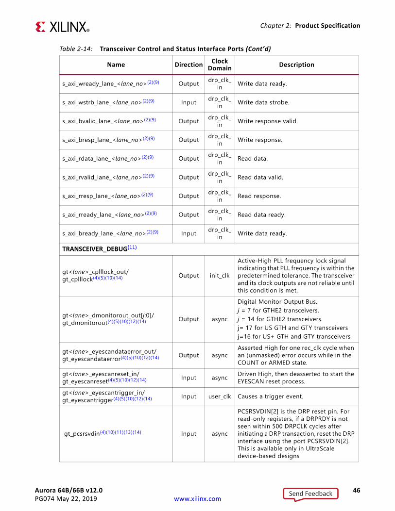
Aurora 64B/66B v12.0 46PG074 May 22, 2019 www.xilinx.com
Chapter 2: Product Specification
s_axi_wready_lane_<lane_no>(2)(9) Output drp_clk_in Write data ready.
s_axi_wstrb_lane_<lane_no>(2)(9) Input drp_clk_in Write data strobe.
s_axi_bvalid_lane_<lane_no>(2)(9) Output drp_clk_in Write response valid.
s_axi_bresp_lane_<lane_no>(2)(9) Output drp_clk_in Write response.
s_axi_rdata_lane_<lane_no>(2)(9) Output drp_clk_in Read data.
s_axi_rvalid_lane_<lane_no>(2)(9) Output drp_clk_in Read data valid.
s_axi_rresp_lane_<lane_no>(2)(9) Output drp_clk_in Read response.
s_axi_rready_lane_<lane_no>(2)(9) Output drp_clk_in Read data ready.
s_axi_bready_lane_<lane_no>(2)(9) Input drp_clk_in Write data ready.
TRANSCEIVER_DEBUG(11)
gt<lane>_cplllock_out/gt_cplllock(4)(5)(10)(14) Output init_clk
Active-High PLL frequency lock signal indicating that PLL frequency is within the predetermined tolerance. The transceiver and its clock outputs are not reliable until this condition is met.
gt<lane>_dmonitorout_out[j:0]/gt_dmonitorout(4)(5)(10)(12)(14) Output async
Digital Monitor Output Bus.j = 7 for GTHE2 transceivers.j = 14 for GTHE2 transceivers.j= 17 for US GTH and GTY transceiversj=16 for US+ GTH and GTY transceivers
gt<lane>_eyescandataerror_out/gt_eyescandataerror(4)(5)(10)(12)(14) Output async
Asserted High for one rec_clk cycle when an (unmasked) error occurs while in the COUNT or ARMED state.
gt<lane>_eyescanreset_in/gt_eyescanreset(4)(5)(10)(12)(14) Input async Driven High, then deasserted to start the
EYESCAN reset process.gt<lane>_eyescantrigger_in/gt_eyescantrigger(4)(5)(10)(12)(14) Input user_clk Causes a trigger event.
gt_pcsrsvdin(4)(10)(11)(13)(14) Input async
PCSRSVDIN[2] is the DRP reset pin. For read-only registers, if a DRPRDY is not seen within 500 DRPCLK cycles after initiating a DRP transaction, reset the DRP interface using the port PCSRSVDIN[2]. This is available only in UltraScale device-based designs
Table 2-14: Transceiver Control and Status Interface Ports (Cont’d)
Name Direction Clock Domain Description
Send Feedback
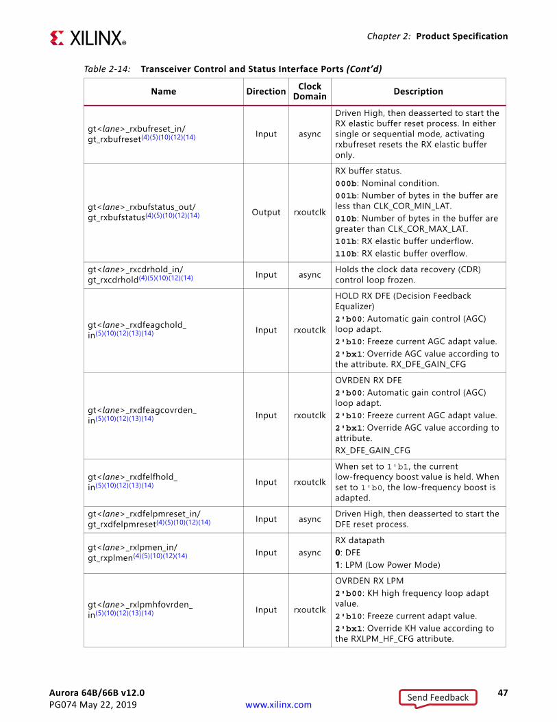
Aurora 64B/66B v12.0 47PG074 May 22, 2019 www.xilinx.com
Chapter 2: Product Specification
gt<lane>_rxbufreset_in/gt_rxbufreset(4)(5)(10)(12)(14) Input async
Driven High, then deasserted to start the RX elastic buffer reset process. In either single or sequential mode, activating rxbufreset resets the RX elastic buffer only.
gt<lane>_rxbufstatus_out/gt_rxbufstatus(4)(5)(10)(12)(14) Output rxoutclk
RX buffer status.000b: Nominal condition.001b: Number of bytes in the buffer are less than CLK_COR_MIN_LAT.010b: Number of bytes in the buffer are greater than CLK_COR_MAX_LAT.101b: RX elastic buffer underflow.110b: RX elastic buffer overflow.
gt<lane>_rxcdrhold_in/gt_rxcdrhold(4)(5)(10)(12)(14) Input async Holds the clock data recovery (CDR)
control loop frozen.
gt<lane>_rxdfeagchold_in(5)(10)(12)(13)(14) Input rxoutclk
HOLD RX DFE (Decision Feedback Equalizer)2'b00: Automatic gain control (AGC) loop adapt.2'b10: Freeze current AGC adapt value.2'bx1: Override AGC value according to the attribute. RX_DFE_GAIN_CFG
gt<lane>_rxdfeagcovrden_in(5)(10)(12)(13)(14) Input rxoutclk
OVRDEN RX DFE2'b00: Automatic gain control (AGC) loop adapt.2'b10: Freeze current AGC adapt value.2'bx1: Override AGC value according to attribute.RX_DFE_GAIN_CFG
gt<lane>_rxdfelfhold_in(5)(10)(12)(13)(14) Input rxoutclk
When set to 1'b1, the current low-frequency boost value is held. When set to 1'b0, the low-frequency boost is adapted.
gt<lane>_rxdfelpmreset_in/gt_rxdfelpmreset(4)(5)(10)(12)(14) Input async Driven High, then deasserted to start the
DFE reset process.
gt<lane>_rxlpmen_in/gt_rxplmen(4)(5)(10)(12)(14) Input async
RX datapath0: DFE1: LPM (Low Power Mode)
gt<lane>_rxlpmhfovrden_in(5)(10)(12)(13)(14) Input rxoutclk
OVRDEN RX LPM2'b00: KH high frequency loop adapt value.2'b10: Freeze current adapt value.2'bx1: Override KH value according to the RXLPM_HF_CFG attribute.
Table 2-14: Transceiver Control and Status Interface Ports (Cont’d)
Name Direction Clock Domain Description
Send Feedback
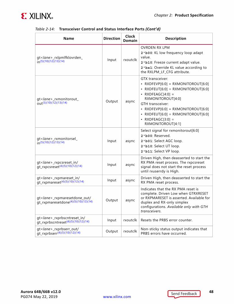
Aurora 64B/66B v12.0 48PG074 May 22, 2019 www.xilinx.com
Chapter 2: Product Specification
gt<lane>_rxlpmlfklovrden_in(5)(10)(12)(13)(14) Input rxoutclk
OVRDEN RX LPM2'b00: KL low frequency loop adapt value.2'b10: Freeze current adapt value.2'bx1: Override KL value according to the RXLPM_LF_CFG attribute.
gt<lane>_rxmonitorout_out(5)(10)(12)(13)(14) Output async
GTX transceiver:• RXDFEVP[6:0] = RXMONITOROUT[6:0]• RXDFEUT[6:0] = RXMONITOROUT[6:0]• RXDFEAGC[4:0] =
RXMONITOROUT[4:0]GTH transceiver:• RXDFEVP[6:0] = RXMONITOROUT[6:0]• RXDFEUT[6:0] = RXMONITOROUT[6:0]• RXDFEAGC[3:0] =
RXMONITOROUT[4:1]
gt<lane>_rxmonitorsel_in(5)(10)(12)(13)(14) Input async
Select signal for rxmonitorout[6:0]2'b00: Reserved.2'b01: Select AGC loop.2'b10: Select UT loop.2'b11: Select VP loop.
gt<lane>_rxpcsreset_in/gt_rxpcsreset(4)(5)(10)(12)(14) Input async
Driven High, then deasserted to start the RX PMA reset process. The rxpcsreset signal does not start the reset process until rxuserrdy is High.
gt<lane>_rxpmareset_in/gt_rxpmareset(4)(5)(10)(12)(14) Input async Driven High, then deasserted to start the
RX PMA reset process.
gt<lane>_rxpmaresetdone_out/gt_rxpmaresetdone(4)(5)(10)(12)(14) Output async
Indicates that the RX PMA reset is complete. Driven Low when GTRXRESET or RXPMARESET is asserted. Available for duplex and RX-only simplex configurations. Available only with GTH transceivers.
gt<lane>_rxprbscntreset_in/gt_rxprbscntreset(4)(5)(10)(12)(14) Input rxoutclk Resets the PRBS error counter.
gt<lane>_rxprbserr_out/gt_rxprbserr(4)(5)(10)(12)(14) Output rxoutclk Non-sticky status output indicates that
PRBS errors have occurred.
Table 2-14: Transceiver Control and Status Interface Ports (Cont’d)
Name Direction Clock Domain Description
Send Feedback
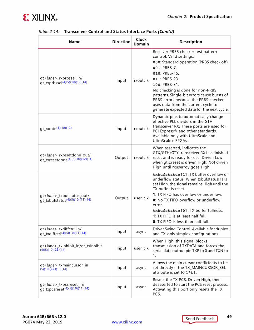
Aurora 64B/66B v12.0 49PG074 May 22, 2019 www.xilinx.com
Chapter 2: Product Specification
gt<lane>_rxprbssel_in/gt_rxprbssel(4)(5)(10)(12)(14) Input rxoutclk
Receiver PRBS checker test pattern control. Valid settings:000: Standard operation (PRBS check off).001: PRBS-7.010: PRBS-15.011: PRBS-23.100: PRBS-31.No checking is done for non-PRBS patterns. Single-bit errors cause bursts of PRBS errors because the PRBS checker uses data from the current cycle to generate expected data for the next cycle.
gt_rxrate(4)(10)(12) Input rxoutclk
Dynamic pins to automatically change effective PLL dividers in the GTH transceiver RX. These ports are used for PCI Express® and other standards. Available only with UltraScale and UltraScale+ FPGAs.
gt<lane>_rxresetdone_out/gt_rxresetdone(4)(5)(10)(12)(14) Output rxoutclk
When asserted, indicates the GTX/GTH/GTY transceiver RX has finished reset and is ready for use. Driven Low when gtrxreset is driven High. Not driven High until rxuserrdy goes High.
gt<lane>_txbufstatus_out/gt_txbufstatus(4)(5)(10)(11)(14) Output user_clk
txbufstatus[1]: TX buffer overflow or underflow status. When txbufstatus[1] is set High, the signal remains High until the TX buffer is reset.1: TX FIFO has overflow or underflow.0: No TX FIFO overflow or underflow error.txbufstatus[0]: TX buffer fullness.1: TX FIFO is at least half full.0: TX FIFO is less than half full.
gt<lane>_txdiffctrl_in/gt_txdiffctrl(4)(5)(10)(11)(14) Input async Driver Swing Control. Available for duplex
and TX-only simplex configurations.
gt<lane>_txinhibit_in/gt_txinhibit(4)(5)(10)(11)(14) Input user_clk
When High, this signal blocks transmission of TXDATA and forces the serial data output pin TXP to 0 and TXN to 1.
gt<lane>_txmaincursor_in (5)(10)(11)(13)(14) Input async
Allows the main cursor coefficients to be set directly if the TX_MAINCURSOR_SEL attribute is set to 1'b1.
gt<lane>_txpcsreset_in/gt_txpcsreset(4)(5)(10)(11)(14) Input async
Resets the TX PCS. Driven High, then deasserted to start the PCS reset process. Activating this port only resets the TX PCS.
Table 2-14: Transceiver Control and Status Interface Ports (Cont’d)
Name Direction Clock Domain Description
Send Feedback
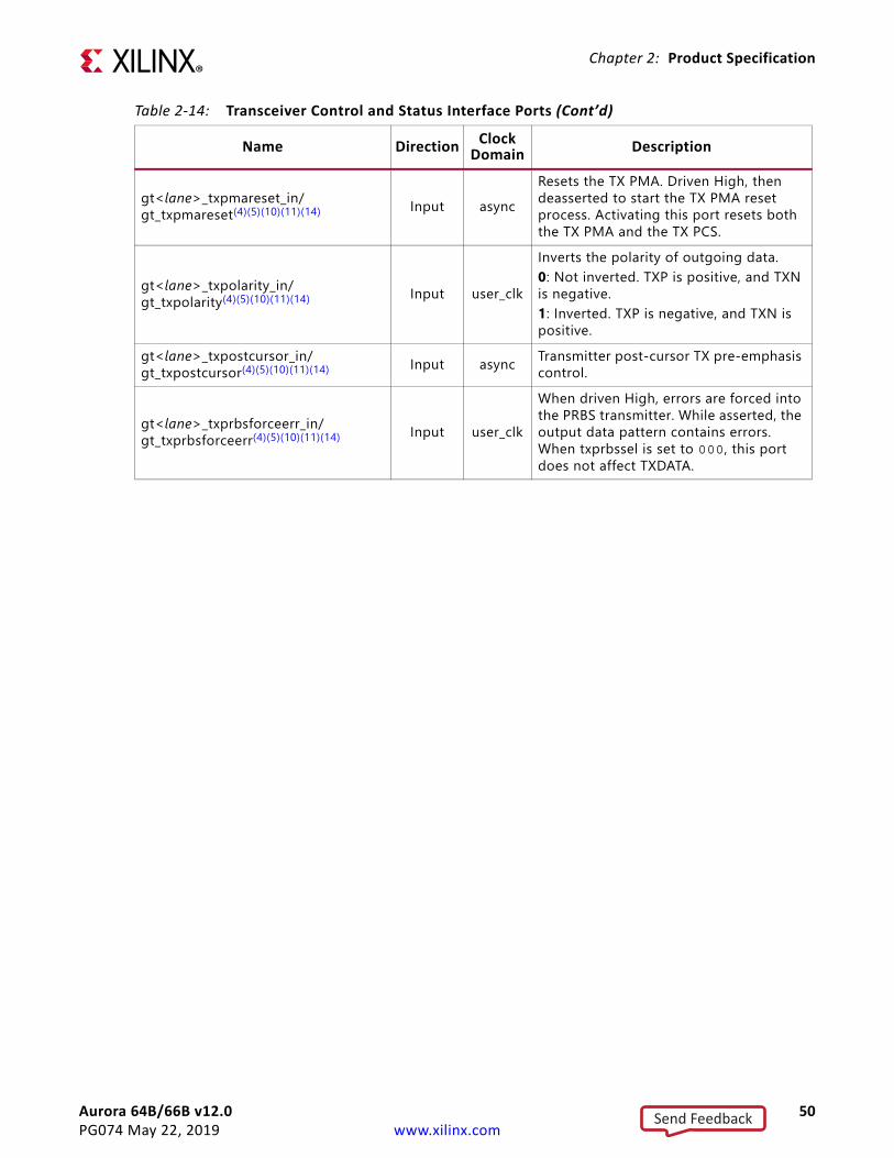
Aurora 64B/66B v12.0 50PG074 May 22, 2019 www.xilinx.com
Chapter 2: Product Specification
gt<lane>_txpmareset_in/gt_txpmareset(4)(5)(10)(11)(14) Input async
Resets the TX PMA. Driven High, then deasserted to start the TX PMA reset process. Activating this port resets both the TX PMA and the TX PCS.
gt<lane>_txpolarity_in/gt_txpolarity(4)(5)(10)(11)(14) Input user_clk
Inverts the polarity of outgoing data.0: Not inverted. TXP is positive, and TXN is negative.1: Inverted. TXP is negative, and TXN is positive.
gt<lane>_txpostcursor_in/gt_txpostcursor(4)(5)(10)(11)(14) Input async Transmitter post-cursor TX pre-emphasis
control.
gt<lane>_txprbsforceerr_in/gt_txprbsforceerr(4)(5)(10)(11)(14) Input user_clk
When driven High, errors are forced into the PRBS transmitter. While asserted, the output data pattern contains errors. When txprbssel is set to 000, this port does not affect TXDATA.
Table 2-14: Transceiver Control and Status Interface Ports (Cont’d)
Name Direction Clock Domain Description
Send Feedback
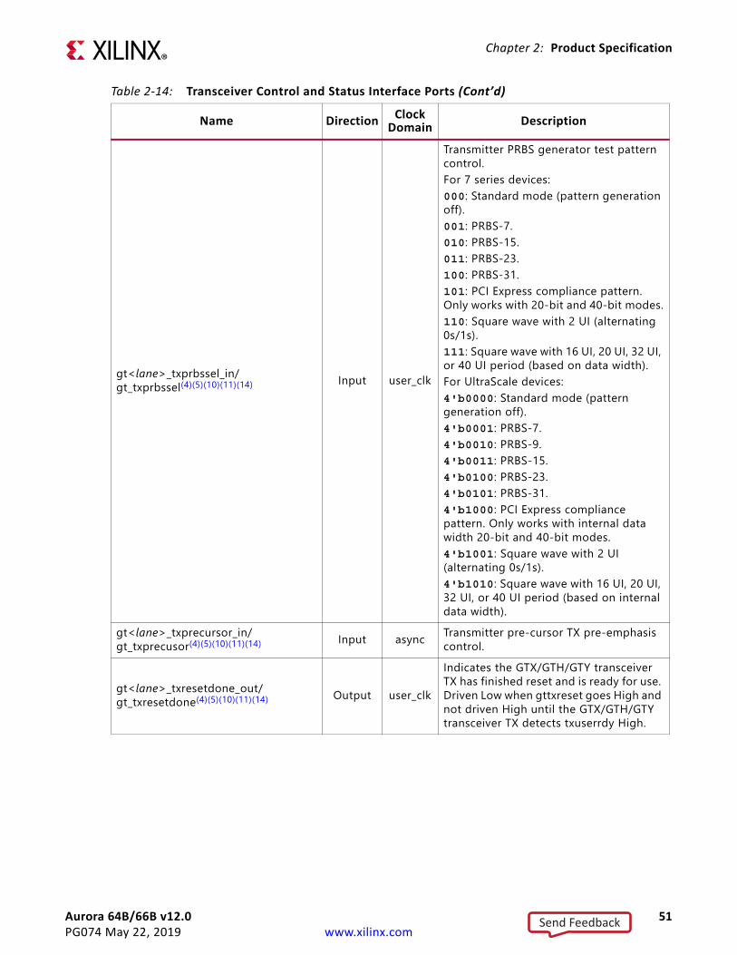
Aurora 64B/66B v12.0 51PG074 May 22, 2019 www.xilinx.com
Chapter 2: Product Specification
gt<lane>_txprbssel_in/gt_txprbssel(4)(5)(10)(11)(14) Input user_clk
Transmitter PRBS generator test pattern control.For 7 series devices:000: Standard mode (pattern generation off).001: PRBS-7.010: PRBS-15.011: PRBS-23.100: PRBS-31.101: PCI Express compliance pattern. Only works with 20-bit and 40-bit modes.110: Square wave with 2 UI (alternating 0s/1s).111: Square wave with 16 UI, 20 UI, 32 UI, or 40 UI period (based on data width).For UltraScale devices:4'b0000: Standard mode (pattern generation off).4'b0001: PRBS-7.4'b0010: PRBS-9.4'b0011: PRBS-15.4'b0100: PRBS-23.4'b0101: PRBS-31.4'b1000: PCI Express compliance pattern. Only works with internal data width 20-bit and 40-bit modes.4'b1001: Square wave with 2 UI (alternating 0s/1s).4'b1010: Square wave with 16 UI, 20 UI, 32 UI, or 40 UI period (based on internal data width).
gt<lane>_txprecursor_in/gt_txprecusor(4)(5)(10)(11)(14) Input async Transmitter pre-cursor TX pre-emphasis
control.
gt<lane>_txresetdone_out/gt_txresetdone(4)(5)(10)(11)(14) Output user_clk
Indicates the GTX/GTH/GTY transceiver TX has finished reset and is ready for use. Driven Low when gttxreset goes High and not driven High until the GTX/GTH/GTY transceiver TX detects txuserrdy High.
Table 2-14: Transceiver Control and Status Interface Ports (Cont’d)
Name Direction Clock Domain Description
Send Feedback
Aurora 64B/66B v12.0 52PG074 May 22, 2019 www.xilinx.com
Chapter 2: Product Specification
IMPORTANT: The ports in the Transceiver Control and Status interface must be driven in accordance with the appropriate GT user guide. Using the input signals listed in Table 2-14 improperly might result in unpredictable behavior of the IP core.
gt_qplllock_quad<quad_no>/gt_qplllock(3)(4)(5)(11)(10) Output init_clk
Active-High PLL frequency lock signal. Indicates that the PLL frequency is within predetermined tolerance. The transceiver and its clock outputs are not reliable until this condition is met.
Notes: 1. m is the number of GTX, GTH or GTY transceivers.2. lane_no varies from 1 to (number of lanes –1).3. In 7 series FPGAs, quad_no varies from 1 to (number of active transceiver quads –1). In UltraScale and UltraScale+
FPGAs, quad_no varies from 1 to the number of active transceiver quads.4. Refer to the UltraScale FPGAs GTH Transceivers User Guide (UG576) [Ref 5] or UltraScale Architecture GTY
Transceivers User Guide (UG578) [Ref 6] for more information about debug ports.5. Refer to the 7 series FPGAs Transceivers User Guide (UG476) [Ref 7] for more information about debug ports.6. In UltraScale and UltraScale+ devices, all DRP and AXI4-Lite ports are sampled on init_clk.7. The Transceiver_Debug ports are enabled if the Additional transceiver control and status ports option is
selected in the Debug and Control section of the Vivado Integrated Design Environment (IDE) Core Options page. For designs using UltraScale and UltraScale+ devices, the prefixes of the optional transceiver debug ports for single-lane cores are changed from gt<lane> to gt, and the postfixes _in and _out are removed. For multi-lane cores, the prefixes of the optional transceiver debug ports gt(n) are aggregated into a single port.
8. This port is available if the Native option is selected in the DRP Mode section of the Vivado IDE Core Options page.
9. This port is available if the AXI4LITE option is selected in the DRP Mode section of the Vivado IDE Core Options page.
10.This port is available if the Additional transceiver control and status ports option is selected in the DRP Mode section of the Vivado IDE Core Options page.
11.Available for duplex, TX-Only simplex and TX/RX_simplex configurations.12.Available for duplex, RX-Only simplex and TX/RX_simplex configurations.13.Not available with UltraScale devices.14.lane varies from 0 to (number of lanes –1).15.quad varies from 0 to (number of active transceiver quads –1).16.Not available in 7 series devices.17.Refer to the relevant UG Transceiver guide for more information on DRP ports.18.For GT Channel DRP access you can either select the AXI4-Lite interface or the native interface.19.GT Common DRP access is not supported.
Table 2-14: Transceiver Control and Status Interface Ports (Cont’d)
Name Direction Clock Domain Description
Send Feedback
Aurora 64B/66B v12.0 53PG074 May 22, 2019 www.xilinx.com
Chapter 2: Product Specification
Figure 2-31 shows the status and control interface for an Aurora 64B/66B duplex core.
Figure 2-32 shows the status and control interface for an Aurora 64B/66B TX-only simplex core.
Figure 2-33 shows the status and control interface for an Aurora 64B/66B RX-only simplex core.
X-Ref Target - Figure 2-31
Figure 2-31: Aurora 64B/66B Duplex Status and Control Interface
X-Ref Target - Figure 2-32
Figure 2-32: Aurora 64B/66B TX-Only Simplex Status and Control Interface
X-Ref Target - Figure 2-33
Figure 2-33: Aurora 64B/66B RX-Only Simplex Status and Control Interface
Status and Control
Interface
loopback[2:0]power_down
reset_pb
txptxn
soft_errchannel_up
hard_err
lane_up
rxprxn
Status and Control
Interface
loopback[2:0]power_downtx_reset_pb
txp[0:m–1]txn[0:m–1]
tx_soft_errtx_channel_up
tx_hard_err
tx_lane_up[0:m–1]
Status and Control
Interface
loopback[2:0]power_downrx_reset_pb
rxp[0:m–1]rxn[0:m–1]
rx_soft_errrx_channel_up
rx_hard_err
rx_lane_up[0:m–1]
Send Feedback
Aurora 64B/66B v12.0 54PG074 May 22, 2019 www.xilinx.com
Chapter 2: Product Specification
Figure 2-34 shows the status and control interface for an Aurora 64B/66B TX/RX Simplex core.
Error Signals in Aurora 64B/66B Cores
Equipment problems and channel noise can cause errors during Aurora 64B/66B channel operation. The 64B/66B encoding method allows the Aurora 64B/66B core to detect some bit errors that can occur in the channel. The core reports these errors by asserting the soft_err signal on every cycle in which they are detected.
The core also monitors each high-speed serial GTX and GTH transceiver for hardware errors such as buffer overflow and loss of lock. Hardware errors are reported by asserting the hard_err signal. Catastrophic hardware errors can also manifest themselves as a burst of soft errors. The Block Sync algorithm described in the Aurora 64B/66B Protocol Specification v1.3 (SP011) [Ref 9] determines whether to treat a burst of soft errors as a hard error.
Whenever a hard error is detected, the core automatically resets itself and attempts to re-initialize. In most cases, this permits reestablishing the Aurora 64B/66B channel when the hardware issue causing the hard error is resolved. Soft errors do not lead to a reset unless enough occur in a short period of time to trigger the block sync state machine.
Table 2-15 describes the core error signals.
X-Ref Target - Figure 2-34
Figure 2-34: Aurora 64B/66B TX/RX Simplex Status and Control Interface
Table 2-15: Aurora 64B/66B Core Error SignalsSignal Description TX RX
hard_err
TX Overflow/Underflow: An overflow or underflow condition exists in the TX data elastic buffer. This condition can occur when the user clock and the reference clock sources are not operating at the same frequency.
X
RX Overflow/Underflow: An overflow or underflow condition exists in the RX data clock correction and channel bonding FIFO. This condition can occur when the clock source frequencies for the two channel partners are not within ±100 ppm.
X
Status and Control
Interface
loopback[2:0]power_downtx_reset_pb
txp[0:m–1]txn[0:m–1]
tx_soft_err
tx_channel_up
tx_hard_err
tx_lane_up[0:m–1]
rxp[0:m–1]rxn[0:m–1]
rx_hard_err
rx_soft_err
rx_channel_up
rx_lane_up[0:m–1]
rx_reset_pb
Send Feedback
Aurora 64B/66B v12.0 55PG074 May 22, 2019 www.xilinx.com
Chapter 2: Product Specification
Initialization
The cores initialize automatically after power-up, reset, or hard error (Figure 2-35). Core modules on each side of the channel perform the Aurora 64B/66B initialization procedure until the channel is ready for use. The lane_up bus indicates which lanes in the channel have finished the lane initialization portion of the procedure. The lane_up signal can be used to help debug equipment problems in a multi-lane channel. channel_up is asserted only after the core completes the entire initialization procedure.
soft_err
Soft Errors: Too many soft errors occurred within a short period of time. The alignment block sync state machine automatically attempts to realign if too many invalid sync headers are detected. Soft errors are not transformed into hard errors.
X
Invalid SYNC Header: The 2-bit header on the 64-bit block was not a valid control or data header. X
Invalid BTF: The block type field (BTF) of a received control block contained an unrecognized value. This condition usually results from a bit error.
X
X-Ref Target - Figure 2-35
Figure 2-35: Initialization Overview
Table 2-15: Aurora 64B/66B Core Error Signals (Cont’d)
Signal Description TX RX
Lane Init
RESET
X13040
Channel Bonding
Wait for Remote
Channel Ready
Single Lane or All Bonded
All Lanes Up
Lost Block Lock
Lost Block Lock
Lost Bonding
Lost Bonding
Remote Ready or Simplex
Remote not
Ready
Lost Block Lock
Send Feedback
Aurora 64B/66B v12.0 56PG074 May 22, 2019 www.xilinx.com
Chapter 2: Product Specification
Aurora 64B/66B cores can receive data before channel_up is asserted. Only the user interface m_axi_rx_tvalid signal should be used to qualify incoming data. Because no transmission can occur until after channel_up is asserted, channel_up can be inverted and used to reset modules that drive the TX side of a full-duplex channel. If user application modules need to be reset before data reception, an inverted lane_up signal can be used for this purpose. Data cannot be received until all of the lane_up signals are asserted.
Aurora 64B/66B Simplex Operation
Simplex Aurora 64B/66B cores have no sideband connection and use timers to declare that the partner is out of initialization and, thus, ready for data transfer. Simplex TX/RX cores have both transmit and receive portions of the transceiver configured to operate independently. However, the simplex TX/RX cores have reset and pma_init signals in common between the transmit and receive path of the core.
The BACKWARD_COMP_MODE3 TX/RX_simplex core parameter can be used to prevent unintentional hot plug events from inhibiting channel up assertion. This parameter is available in the <user_component_name>_core.v file and is available for all core configurations.
• BACKWARD_COMP_MODE3 = 0 clears the hot plug counter only on reception of CC characters
• BACKWARD_COMP_MODE3 = 1 clears the hot plug counter on reception of any valid BTF characters
RECOMMENDED: Follow the reset sequence given in Chapter 3.
Auto Link Recovery for Simplex
The simplex Aurora 64b/66b core must follow a predefined reset sequence for the simplex cores to link up and work as expected. The simplex TX core needs to be in reset or should keep sending initialization sequences until the RX side is up. As part of RX link recovery, polarity inversion and other IP specific checks are to re-negotiate the link. If a change in polarity occurs during runtime, the core requires a complete reset sequence to recover.
The simplex auto link recovery feature in the core eliminates this requirement, thereby removing any reset sequence requirement between simplex TX and simplex RX cores.
Auto Link Recovery in Aurora 64b/66b simplex designs is based on the reception of Channel Bonding (CB) patterns. Reception of the pattern allows the RX simplex core to come up independently of the TX Simplex core bring-up. The parameter PERIODIC_CB_COUNT denotes in user_clk cycles the time from the start of one periodic CB pattern to the start of the next successive CB pattern. The minimum value is 6,080. The maximum value is 163,839. The periodic CB pattern includes transmission of CB-IDLE patterns with the appropriate spacing to help the receiver achieve channel up even if the link was down for some reason. Typically, these CB-IDLE patterns take up to 600 user-clk cycles. Spacing of
Send Feedback
Aurora 64B/66B v12.0 57PG074 May 22, 2019 www.xilinx.com
Chapter 2: Product Specification
these patterns are chosen to match the throughput of the earlier released core versions which were transmitting a Single CB character periodically.
Bandwidth occupancy = Number of user_clk cycles required by CB pattern/ Total number of user_clk cycles)*100.
You can increase the count based on the following formula:
PERIODIC_CB_COUNT = Minimum {1048570, INTEGER part of [{16777215*INIT_CLK_PERIOD}/{4*USER_CLK_PERIOD}]}
where,
INIT_CLK_PERIOD is init_clk time-period in ns
USER_CLK_PERIOD is user_clk time-period in ns.
IMPORTANT: Xilinx highly recommends that the maximum value be fixed at 163,839 and a change in the value should be performed with careful analysis and testing.
DRP Interface
The DRP interface allows user applications to monitor and modify the transceiver status. The native interface provides the native transceiver DRP interface ports. The AXI4-Lite interface (fully compliant with the AXI4-Lite protocol) is the default interface.
For native DRP sequences, the read and write operations are as specified in the respective FPGA Transceivers User Guides. For AXI4-Lite DRP sequences, the read and write operations from the user interface are specified in the AXI4-Lite protocol. The Aurora 64B/66B core does not use the wstrb signal (refer to the Vivado AXI Reference Guide, (UG1037) [Ref 10]). The axi_to_drp module is used to translate between the transceiver DRP and AXI4-Lite protocols.
Transceiver Debug Interface
Figure 2-36 and Figure 2-37 show the additional available transceiver debugging control and status ports when the TRANSCEIVER DEBUG interface is selected for 7 series and UltraScale devices, respectively.
Send Feedback
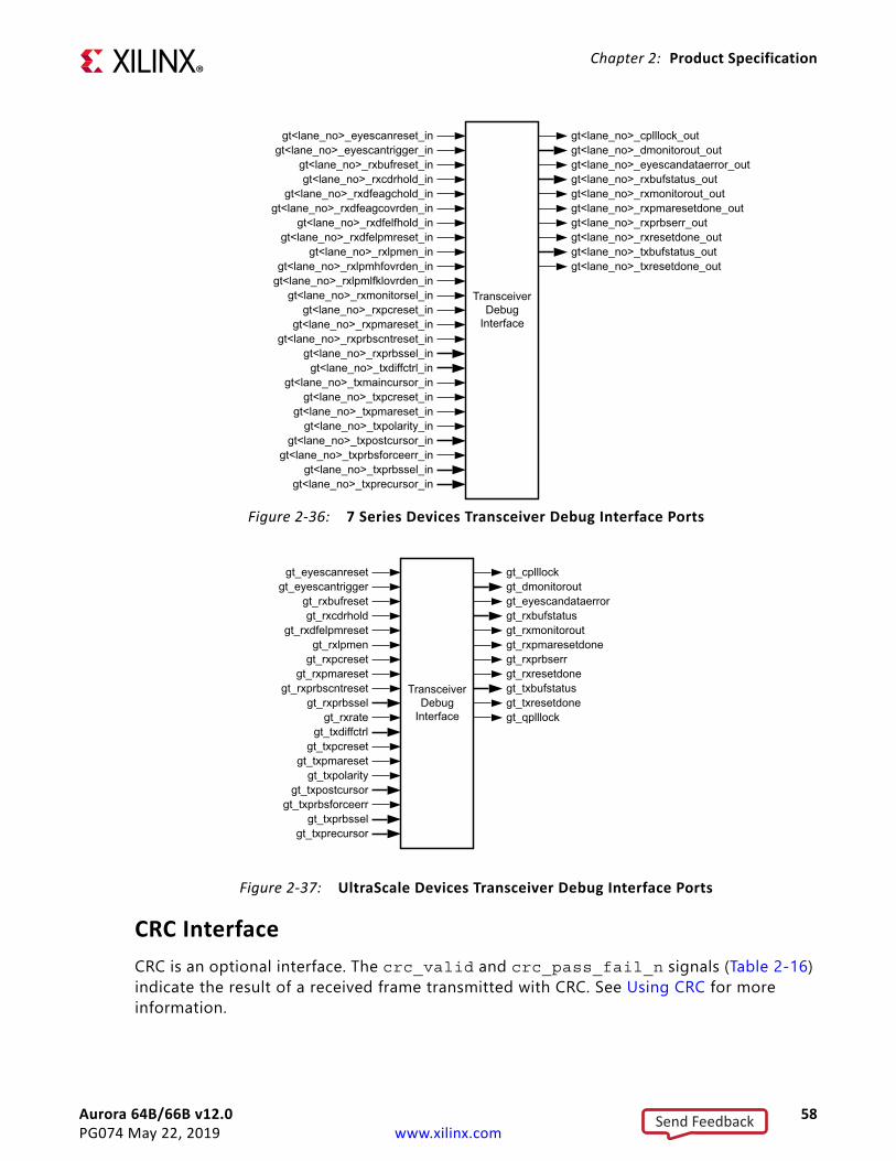
Aurora 64B/66B v12.0 58PG074 May 22, 2019 www.xilinx.com
Chapter 2: Product Specification
CRC InterfaceCRC is an optional interface. The crc_valid and crc_pass_fail_n signals (Table 2-16) indicate the result of a received frame transmitted with CRC. See Using CRC for more information.
X-Ref Target - Figure 2-36
Figure 2-36: 7 Series Devices Transceiver Debug Interface PortsX-Ref Target - Figure 2-37
Figure 2-37: UltraScale Devices Transceiver Debug Interface Ports
Transceiver Debug
Interface
gt<lane_no>_txprbssel_ingt<lane_no>_txprecursor_in
gt<lane_no>_txmaincursor_ingt<lane_no>_txpcreset_in
gt<lane_no>_txpmareset_ingt<lane_no>_txpolarity_in
gt<lane_no>_txpostcursor_in
gt<lane_no>_cplllock_outgt<lane_no>_dmonitorout_outgt<lane_no>_eyescandataerror_outgt<lane_no>_rxbufstatus_out
gt<lane_no>_txprbsforceerr_in
gt<lane_no>_rxprbssel_ingt<lane_no>_txdiffctrl_in
gt<lane_no>_rxlpmhfovrden_ingt<lane_no>_rxlpmlfklovrden_in
gt<lane_no>_rxmonitorsel_ingt<lane_no>_rxpcreset_in
gt<lane_no>_rxpmareset_ingt<lane_no>_rxprbscntreset_in
gt<lane_no>_rxdfelpmreset_ingt<lane_no>_rxlpmen_in
gt<lane_no>_eyescantrigger_ingt<lane_no>_rxbufreset_ingt<lane_no>_rxcdrhold_in
gt<lane_no>_rxdfeagchold_ingt<lane_no>_rxdfeagcovrden_in
gt<lane_no>_rxdfelfhold_in
gt<lane_no>_eyescanreset_in
gt<lane_no>_rxmonitorout_outgt<lane_no>_rxpmaresetdone_outgt<lane_no>_rxprbserr_outgt<lane_no>_rxresetdone_outgt<lane_no>_txbufstatus_outgt<lane_no>_txresetdone_out
Transceiver Debug
Interface
gt_txprbsselgt_txprecursor
gt_txdiffctrlgt_txpcreset
gt_txpmaresetgt_txpolarity
gt_txpostcursor
gt_cplllockgt_dmonitoroutgt_eyescandataerrorgt_rxbufstatus
gt_txprbsforceerr
gt_rxprbsselgt_rxrate
gt_rxcdrholdgt_rxdfelpmreset
gt_rxlpmengt_rxpcreset
gt_rxpmaresetgt_rxprbscntreset
gt_eyescantriggergt_rxbufreset
gt_eyescanreset
gt_rxmonitoroutgt_rxpmaresetdonegt_rxprbserrgt_rxresetdonegt_txbufstatusgt_txresetdonegt_qplllock
Send Feedback
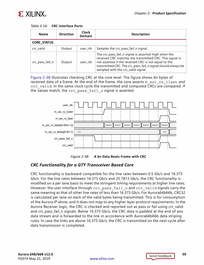
Aurora 64B/66B v12.0 59PG074 May 22, 2019 www.xilinx.com
Chapter 2: Product Specification
Figure 2-38 illustrates checking CRC at the core level. The figure shows 6n bytes of received data of a frame. At the end of the frame, the core asserts m_axi_rx_tlast and crc_valid. In the same clock cycle the transmitted and computed CRCs are compared. If the values match, the crc_pass_fail_n signal is asserted.
CRC Functionality for a GTY Transceiver Based Core
CRC functionality is backward compatible for the line rates between 0.5 Gb/s and 16.375 Gb/s. For the line rates between 16.375 Gb/s and 25.7813 Gb/s, the CRC functionality is modified on a per lane basis to meet the stringent timing requirements at higher line rates. However, the user interface through crc_pass_fail_n and crc_valid signals carry the same meaning as that of other line rates of less than 16.375 Gb/s. For Aurora64b66b, CRC32 is calculated per lane on each of the valid bytes being transmitted. This is for consumption of the Aurora IP alone, and it does not map to any higher layer protocol requirements. In the Aurora Receiver logic, the CRC is checked and reported out as pass or fail using crc_valid and crc_pass_fail_n signals. Below 16.375 Gb/s, the CRC data is padded at the end of axis data stream and is forwarded to the link in accordance with Aurora64b66b data striping rules. In case the links are above 16.375 Gb/s, the CRC is transmitted on the next cycle after data transmission is completed.
Table 2-16: CRC Interface Ports
Name Direction Clock Domain Description
CORE_STATUScrc_valid Output user_clk Samples the crc_pass_fail_n signal.
crc_pass_fail_n Output user_clk
The crc_pass_fail_n signal is asserted High when the received CRC matches the transmitted CRC. This signal is not asserted if the received CRC is not equal to the transmitted CRC. The crc_pass_fail_n signal should always be sampled with the crc_valid signal.
X-Ref Target - Figure 2-38
Figure 2-38: A 6n Data Beats Frame with CRC
user_clk
m_axi_rx_tvalid
m_axi_rx_tlast
m_axi_rx_tdata[0:(64n-1)]
m_axi_rx_tkeep[0:8n-1]
crc_pass_fail_n
crc_valid
Databeat 0 Databeat 1 Databeat 2 Databeat 3 Databeat 4 Databeat 5 Databeat 6
0xFF 0xF0
Send Feedback
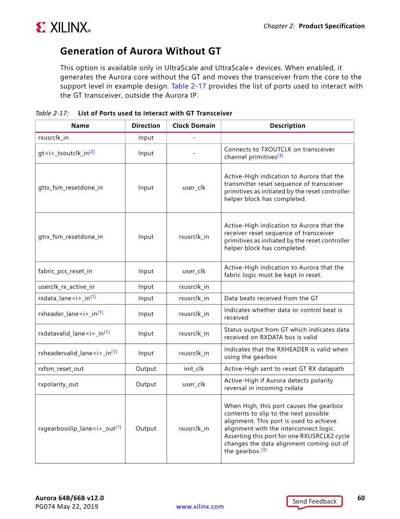
Aurora 64B/66B v12.0 60PG074 May 22, 2019 www.xilinx.com
Chapter 2: Product Specification
Generation of Aurora Without GTThis option is available only in UltraScale and UltraScale+ devices. When enabled, it generates the Aurora core without the GT and moves the transceiver from the core to the support level in example design. Table 2-17 provides the list of ports used to interact with the GT transceiver, outside the Aurora IP.
Table 2-17: List of Ports used to interact with GT TransceiverName Direction Clock Domain Description
rxusrclk_in Input -
gt<i>_txoutclk_in(2) Input - Connects to TXOUTCLK on transceiver channel primitives(3)
gttx_fsm_resetdone_in Input user_clkActive-High indication to Aurora that the transmitter reset sequence of transceiver primitives as initiated by the reset controller helper block has completed.
gtrx_fsm_resetdone_in Input rxusrclk_inActive-High indication to Aurora that the receiver reset sequence of transceiver primitives as initiated by the reset controller helper block has completed.
fabric_pcs_reset_in Input user_clk Active-High indication to Aurora that the fabric logic must be kept in reset.
userclk_rx_active_in Input rxusrclk_inrxdata_lane<i>_in(1) Input rxusrclk_in Data beats received from the GT
rxheader_lane<i>_in(1) Input rxusrclk_in Indicates whether data or control beat is received
rxdatavalid_lane<i>_in(1) Input rxusrclk_in Status output from GT which indicates data received on RXDATA bus is valid
rxheadervalid_lane<i>_in(1) Input rxusrclk_in Indicates that the RXHEADER is valid when using the gearbox
rxfsm_reset_out Output init_clk Active-High sent to reset GT RX datapath
rxpolarity_out Output user_clk Active-High if Aurora detects polarity reversal in incoming rxdata
rxgearboxslip_lane<i>_out(1) Output rxusrclk_in
When High, this port causes the gearbox contents to slip to the next possible alignment. This port is used to achieve alignment with the interconnect logic. Asserting this port for one RXUSRCLK2 cycle changes the data alignment coming out of the gearbox.(3)
Send Feedback
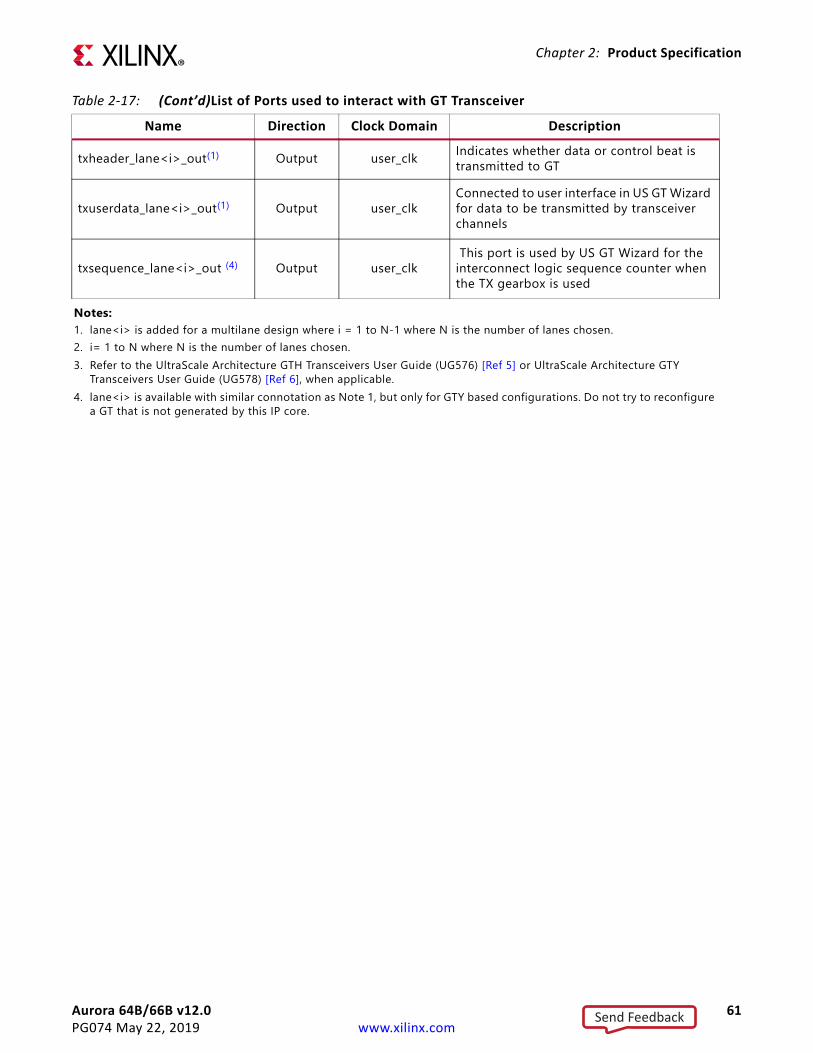
Aurora 64B/66B v12.0 61PG074 May 22, 2019 www.xilinx.com
Chapter 2: Product Specification
txheader_lane<i>_out(1) Output user_clk Indicates whether data or control beat is transmitted to GT
txuserdata_lane<i>_out(1) Output user_clkConnected to user interface in US GT Wizard for data to be transmitted by transceiver channels
txsequence_lane<i>_out (4) Output user_clk This port is used by US GT Wizard for the interconnect logic sequence counter when the TX gearbox is used
Notes: 1. lane<i> is added for a multilane design where i = 1 to N-1 where N is the number of lanes chosen.2. i= 1 to N where N is the number of lanes chosen.3. Refer to the UltraScale Architecture GTH Transceivers User Guide (UG576) [Ref 5] or UltraScale Architecture GTY
Transceivers User Guide (UG578) [Ref 6], when applicable.4. lane<i> is available with similar connotation as Note 1, but only for GTY based configurations. Do not try to reconfigure
a GT that is not generated by this IP core.
Table 2-17: (Cont’d)List of Ports used to interact with GT TransceiverName Direction Clock Domain Description
Send Feedback
Aurora 64B/66B v12.0 62PG074 May 22, 2019 www.xilinx.com
Chapter 3
Designing with the CoreThis chapter includes guidelines and additional information to facilitate designing with the core.
General Design GuidelinesAll Aurora 64B/66B core implementations require careful attention to system performance requirements. Pipelining, logic mappings, placement constraints, and logic duplications are all methods that help boost system performance.
Keep It RegisteredTo simplify timing and increase system performance in an FPGA design, keep all inputs and outputs registered with a flip-flop between the user application and the core. While registering signals might not be possible for all paths, it simplifies timing analysis and makes it easier for the Xilinx tools to place-and-route the design.
Recognize Timing Critical SignalsThe XDC file provided with the example design for the core identifies the critical signals and the timing constraints that should be applied.
Make Only Allowed ModificationsThe Aurora 64B/66B core is not user modifiable. Any modifications might have adverse effects on the system timings and protocol compliance. Supported user configurations of the Aurora 64B/66B core can only be made by selecting options from the IP catalog.
Send Feedback
Aurora 64B/66B v12.0 63PG074 May 22, 2019 www.xilinx.com
Chapter 3: Designing with the Core
ClockingGood clocking is critical for the correct operation of the Aurora 64B/66B core. The core requires a low-jitter reference clock to drive the high-speed TX clock and clock recovery circuits in the GTX, GTH or GTY transceiver. The core also requires at least one frequency-locked parallel clock for synchronous operation with the user application.
Each Aurora 64B/66B core is generated in the example_project directory which includes a design called aurora_example. This design instantiates the generated core and demonstrates a working clock configuration for the core. First-time users should examine the Aurora 64B/66B example design for use as a template when connecting the clock interface.
Send Feedback
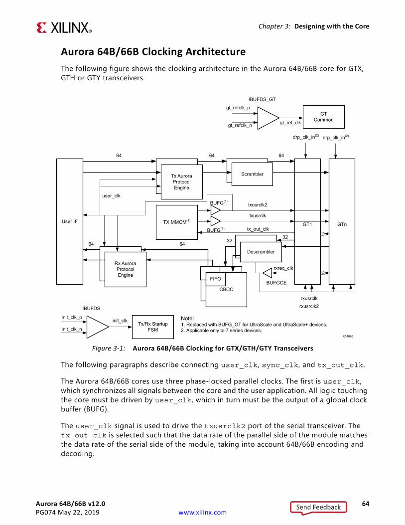
Aurora 64B/66B v12.0 64PG074 May 22, 2019 www.xilinx.com
Chapter 3: Designing with the Core
Aurora 64B/66B Clocking ArchitectureThe following figure shows the clocking architecture in the Aurora 64B/66B core for GTX, GTH or GTY transceivers.
The following paragraphs describe connecting user_clk, sync_clk, and tx_out_clk.
The Aurora 64B/66B cores use three phase-locked parallel clocks. The first is user_clk, which synchronizes all signals between the core and the user application. All logic touching the core must be driven by user_clk, which in turn must be the output of a global clock buffer (BUFG).
The user_clk signal is used to drive the txusrclk2 port of the serial transceiver. The tx_out_clk is selected such that the data rate of the parallel side of the module matches the data rate of the serial side of the module, taking into account 64B/66B encoding and decoding.
X-Ref Target - Figure 3-1
Figure 3-1: Aurora 64B/66B Clocking for GTX/GTH/GTY Transceivers
Note: 1. Replaced with BUFG_GT for UltraScale and UltraScale+ devices.2. Applicable only to 7 series devices.
User IF
Tx Aurora ProtocolEngine
TX MMCM(1)
Rx Aurora ProtocolEngine
Scrambler
Descrambler
GT1 GTn
GTCommon
Tx/Rx StartupFSM
IBUFDS
init_clk
IBUFDS_GT
gt_ref_clk
drp_clk_in(2) drp_clk_in(2)
646464
64 6432
32
txusrclk2
txusrclk
BUFG(1)
BUFG(1)
user_clk
rxrec_clk
rxusrclkrxusrclk2
BUFGCE
tx_out_clk
CBCC
FIFO
X14096
gt_refclk_p
Init_clk_p
gt_refclk_n
Init_clk_n
Send Feedback
Aurora 64B/66B v12.0 65PG074 May 22, 2019 www.xilinx.com
Chapter 3: Designing with the Core
The third phase-locked parallel clock is sync_clk. This clock must also come from a BUFG and is used to drive txusrclk port of the serial transceiver. It is also connected to the Aurora 64B/66B core to drive the internal synchronization logic of the serial transceiver.
To make it easier to use the two parallel clocks, a clock module is provided in a subdirectory called clock_module under example_design/support or under src based on shared logic settings. The ports for this module are described in Table 2-14. If the clock module is used, the mmcm_not_locked signal should be connected to the mmcm_not_locked output of the clock module; tx_out_clk should connect to the clock module clk port, and pll_lock should connect to the clock module pll_not_locked port. If the clock module is not used, connect the mmcm_not_locked signal to the inverse of the locked signal from any PLL used to generate either of the parallel clocks, and use the pll_lock signal to hold the PLLs in reset during stabilization if tx_out_clk is used as the PLL source clock. The txusrclk could be unreliable during assertion of pma_init; hence, the core uses a stable clock (init_clk) for MMCM synchronization. Using a stable clock to sample adds more robustness to the link.
If MMCM is used to generate a stable clock (init_clk), pma_init needs to be applied to the Aurora 64B/66B core until MMCM lock is established. This ensures that the core remains in a known state before a stable clock is available for the core.
Usage of BUFG in the Aurora 64B/66B CoreThe Aurora 64B/66B core uses four BUFGs as shown in Figure 3-1 for a given core configuration using GTX or GTH transceivers. Aurora 64B/66B is an eight-byte-aligned protocol, and the datapath from the user interface is 8-bytes aligned. For GTX and GTH transceivers, the core configures the transmit path as eight bytes and the receive path as four bytes.
The CB/CC logic is internal to the core, which is primarily based on the received recovered clock from the serial transceiver. The BUFG usage is constant for any core configuration and does not increase with any core feature. In GTY transceiver, the core configures both transmit and receive path as eight bytes.
Reference Clocks for FPGA DesignsAurora 64B/66B cores require low-jitter reference clocks for generating and recovering high-speed serial clocks in the GTX, GTH or GTY transceivers. Each reference clock can be set to the reference clock input ports: gtxq/gthq/gtyq. Reference clocks should be driven with high-quality clock sources whenever possible to decrease jitter and prevent bit errors. DCMs should never be used to drive reference clocks, because they introduce too much jitter.
For UltraScale™ and UltraScale+ devices, the Xilinx implementation tools make necessary adjustments to the north-south routing and the pin swapping necessary to the GT
Send Feedback
Aurora 64B/66B v12.0 66PG074 May 22, 2019 www.xilinx.com
Chapter 3: Designing with the Core
transceiver clock inputs to route clocks from one quad to another, when required, based on the clock location constraints mentioned in example design xdc file.
The following rules must be observed when sharing a reference clock to ensure that jitter margins for high-speed designs are met:
• In 7 series FPGAs, the total number of GTX or GTH transceiver quads sourced by an external clock pin pair must not exceed three quads (one quad above and one quad below), or 12 GTXE2_CHANNEL/GTHE2_CHANNEL transceivers. Designs in 7 series FPGAs with more than 12 transceivers or more than three quads should use multiple external clock pins. See the 7 Series FPGAs GTX/GTH Transceivers User Guide (UG476) [Ref 7].
• In UltraScale FPGAs, the total number of transceiver quads sourced by an external clock pin pair must not exceed five quads (two quads above and two quads below), or twenty GTHE3/GTHE4_CHANNEL transceivers. See the UltraScale FPGAs GTH Transceivers User Guide (UG576) [Ref 5].
• For GTY core configuration and line rate > 16.375G, the Aurora 64b66b core will default to active transceiver Quads GTREFCLK. Each Quads GT Refclk should be individually fed. For more details, see UltraScale Architecture GTY Transceivers User Guide (UG578) [Ref 6]. Manual editing of the transceiver attributes is not recommended but can be performed following the recommendations in the aforementioned GT user guides.
Clock relationship with the line rates in Aurora core are as follows.
The following table shows PLL and the corresponding line rate selections.
Table 3-1: Clock Relationship with Line Rates in Aurora Core
Clock Line Rate Description
TX/RXUSRCLK Rate Line Rate / Internal Datapath Width. TX/RXUSRCLK2 Rate follows Table 3-10 of UG576/UG578
7-Series devices and GTHE3/GTHE4 transceivers
TX_DATA_WIDTH is 64TX_INT_DATAWIDTH, RX_DATA_WIDTH and RX_INT_DATAWIDTH are 32.
For GTYE3/GTYE4 transceivers
TX_DATA_WIDTH, TX_INT_DATAWIDTH,RX_DATA_WIDTH, RX_INT_DATAWIDTH are selected as 64.
Table 3-2: PLL and Corresponding Line Rate Selections PLL Selection Line Rates in Gbps
UltraScale CPLL <=8QPLL1 or QPLL0 (if QPLL1 not available) >8 and <=13QPLL0 or QPLL1 (if QPLL0 not available) >13 and <=16.375QPLL1 or QPLL0 (if QPLL1 not available) >16.375 and <=19.6QPLL0 Other line rates
Send Feedback
Aurora 64B/66B v12.0 67PG074 May 22, 2019 www.xilinx.com
Chapter 3: Designing with the Core
Reset and Power DownResetThe reset_pb signal is used to restore the Aurora 64B/66B core to a known starting state. Upon reset, the core stops the current operation and re-initializes the channel. It is expected that user_clock is stable when the reset_pb signal is applied. When the reset_pb signal to the Aurora 64B/66B channel partner1 is asserted, channel partner2 also loses lock. Channel partner2 regains lock when channel partner1 is out of reset and begins transmitting valid patterns. On full-duplex cores the reset_pb signal resets both the TX and RX sides of the channel. simplex Aurora 64B/66B cores have similar reset_pb ports for both partners and require a different reset sequence. Asserting pma_init resets the entire serial transceiver which eventually resets the Aurora 64B/66B core as well. Also, it is assumed init_clk is always stable and the ref_clk is stable at the time of deassertion of the pma_init signal.
Reset SequenceThe following are recommended reset sequences for the Aurora 64B/66B core at the example design level for the available dataflow configurations.
Note: In the reset sequence diagrams the init_clk is added for illustration; both reset_pb and pma_init are asynchronous resets to the core.
Aurora 64B/66B Duplex
During the board power-on sequence, both the pma_init and reset_pb signals are expected to be High. INIT_CLK and GT_REFCLK are expected to be stable during power-on for the proper functioning of the Aurora 64B/66B core. When both clocks are stable, pma_init is deasserted followed by the deassertion of reset_pb.
7 Series CPLL <8QPLL >8
Table 3-2: (Cont’d)PLL and Corresponding Line Rate Selections PLL Selection Line Rates in Gbps
Send Feedback
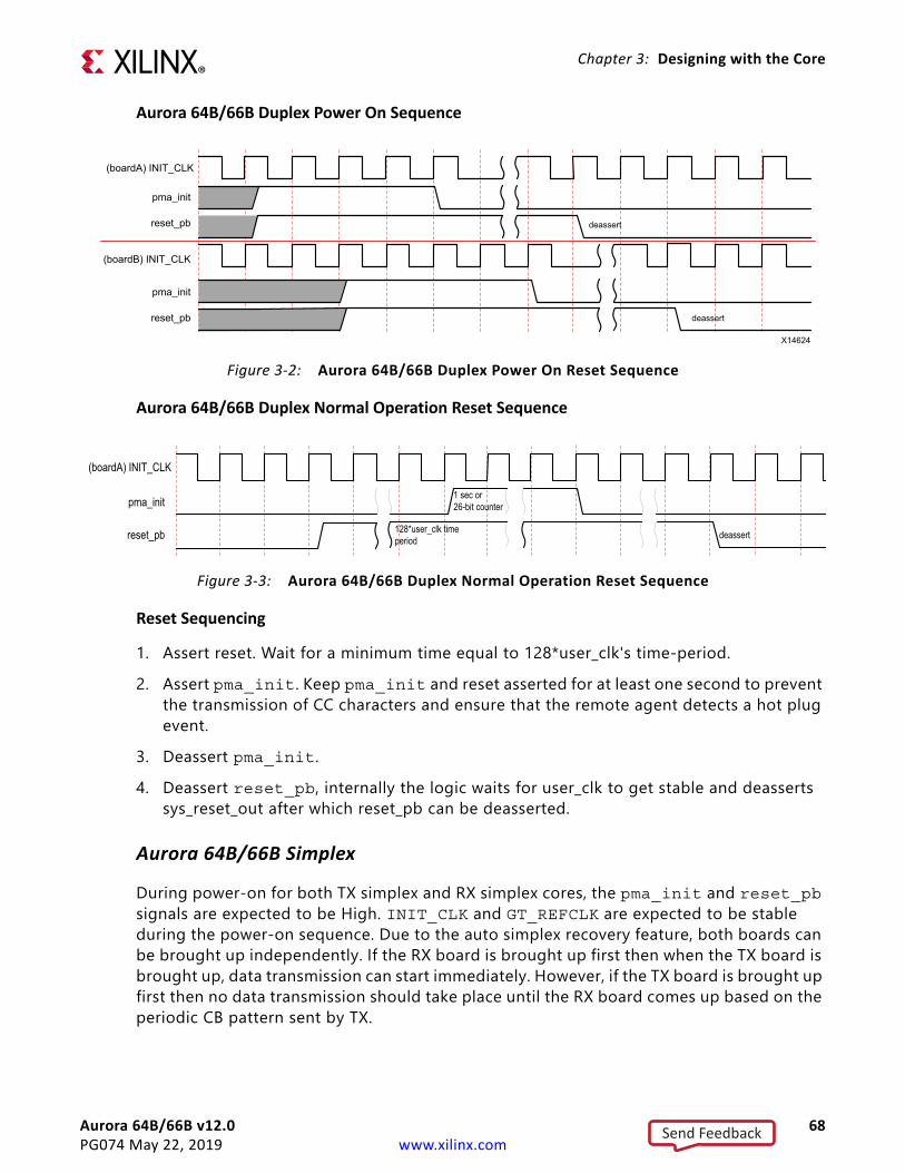
Aurora 64B/66B v12.0 68PG074 May 22, 2019 www.xilinx.com
Chapter 3: Designing with the Core
Aurora 64B/66B Duplex Power On Sequence
Aurora 64B/66B Duplex Normal Operation Reset Sequence
Reset Sequencing
1. Assert reset. Wait for a minimum time equal to 128*user_clk's time-period.2. Assert pma_init. Keep pma_init and reset asserted for at least one second to prevent
the transmission of CC characters and ensure that the remote agent detects a hot plug event.
3. Deassert pma_init.4. Deassert reset_pb, internally the logic waits for user_clk to get stable and deasserts
sys_reset_out after which reset_pb can be deasserted.
Aurora 64B/66B Simplex
During power-on for both TX simplex and RX simplex cores, the pma_init and reset_pb signals are expected to be High. INIT_CLK and GT_REFCLK are expected to be stable during the power-on sequence. Due to the auto simplex recovery feature, both boards can be brought up independently. If the RX board is brought up first then when the TX board is brought up, data transmission can start immediately. However, if the TX board is brought up first then no data transmission should take place until the RX board comes up based on the periodic CB pattern sent by TX.
X-Ref Target - Figure 3-2
Figure 3-2: Aurora 64B/66B Duplex Power On Reset Sequence
pma_init
reset_pb
(boardA) INIT_CLK
X14624
deassert
deassert
(boardB) INIT_CLK
pma_init
reset_pb
X-Ref Target - Figure 3-3
Figure 3-3: Aurora 64B/66B Duplex Normal Operation Reset Sequence
pma_init
reset_pb
(boardA) INIT_CLK
128*user_clk time period
1 sec or26-bit counter
deassert
Send Feedback
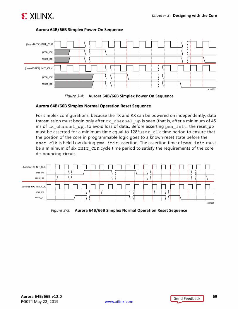
Aurora 64B/66B v12.0 69PG074 May 22, 2019 www.xilinx.com
Chapter 3: Designing with the Core
Aurora 64B/66B Simplex Power On Sequence
Aurora 64B/66B Simplex Normal Operation Reset Sequence
For simplex configurations, because the TX and RX can be powered on independently, data transmission must begin only after rx_channel_up is seen (that is, after a minimum of 45 ms of tx_channel_up), to avoid loss of data., Before asserting pma_init, the reset_pb must be asserted for a minimum time equal to 128*user_clk time period to ensure that the portion of the core in programmable logic goes to a known reset state before the user_clk is held Low during pma_init assertion. The assertion time of pma_init must be a minimum of six INIT_CLK cycle time period to satisfy the requirements of the core de-bouncing circuit.
X-Ref Target - Figure 3-4
Figure 3-4: Aurora 64B/66B Simplex Power On Sequence
pma_init
reset_pb
(boardA TX) INIT_CLK
X14632
(boardB RX) INIT_CLK
pma_init
reset_pb
X-Ref Target - Figure 3-5
Figure 3-5: Aurora 64B/66B Simplex Normal Operation Reset Sequence
pma_init
reset_pb
(boardA TX) INIT_CLK
X14631
(boardB RX) INIT_CLK
pma_init
reset_pb
Send Feedback
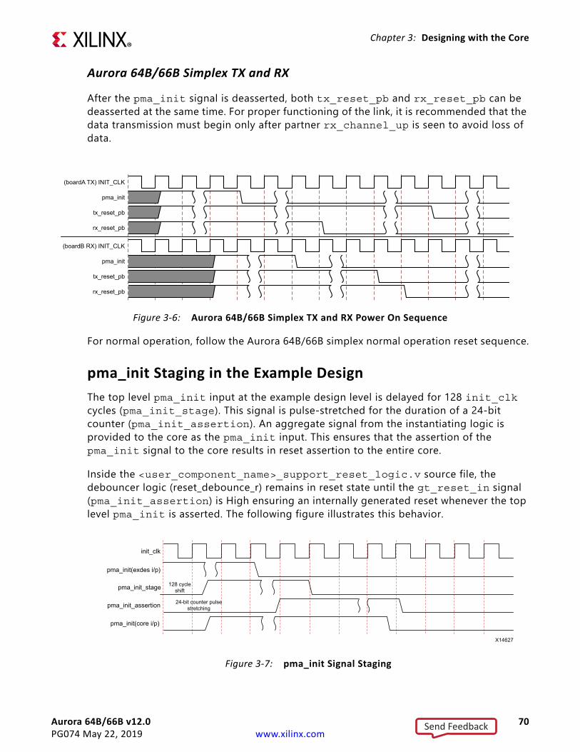
Aurora 64B/66B v12.0 70PG074 May 22, 2019 www.xilinx.com
Chapter 3: Designing with the Core
Aurora 64B/66B Simplex TX and RX
After the pma_init signal is deasserted, both tx_reset_pb and rx_reset_pb can be deasserted at the same time. For proper functioning of the link, it is recommended that the data transmission must begin only after partner rx_channel_up is seen to avoid loss of data.
For normal operation, follow the Aurora 64B/66B simplex normal operation reset sequence.
pma_init Staging in the Example DesignThe top level pma_init input at the example design level is delayed for 128 init_clk cycles (pma_init_stage). This signal is pulse-stretched for the duration of a 24-bit counter (pma_init_assertion). An aggregate signal from the instantiating logic is provided to the core as the pma_init input. This ensures that the assertion of the pma_init signal to the core results in reset assertion to the entire core.
Inside the <user_component_name>_support_reset_logic.v source file, the debouncer logic (reset_debounce_r) remains in reset state until the gt_reset_in signal (pma_init_assertion) is High ensuring an internally generated reset whenever the top level pma_init is asserted. The following figure illustrates this behavior.
X-Ref Target - Figure 3-6
Figure 3-6: Aurora 64B/66B Simplex TX and RX Power On Sequence
(boardA TX) INIT_CLK
pma_init
tx_reset_pb
rx_reset_pb
(boardB RX) INIT_CLK
pma_init
tx_reset_pb
rx_reset_pb
X-Ref Target - Figure 3-7
Figure 3-7: pma_init Signal Staging
pma_init(exdes i/p)
pma_init_stage
init_clk
X14627
128 cycle shift
pma_init_assertion
pma_init(core i/p)
24-bit counter pulse stretching
Send Feedback
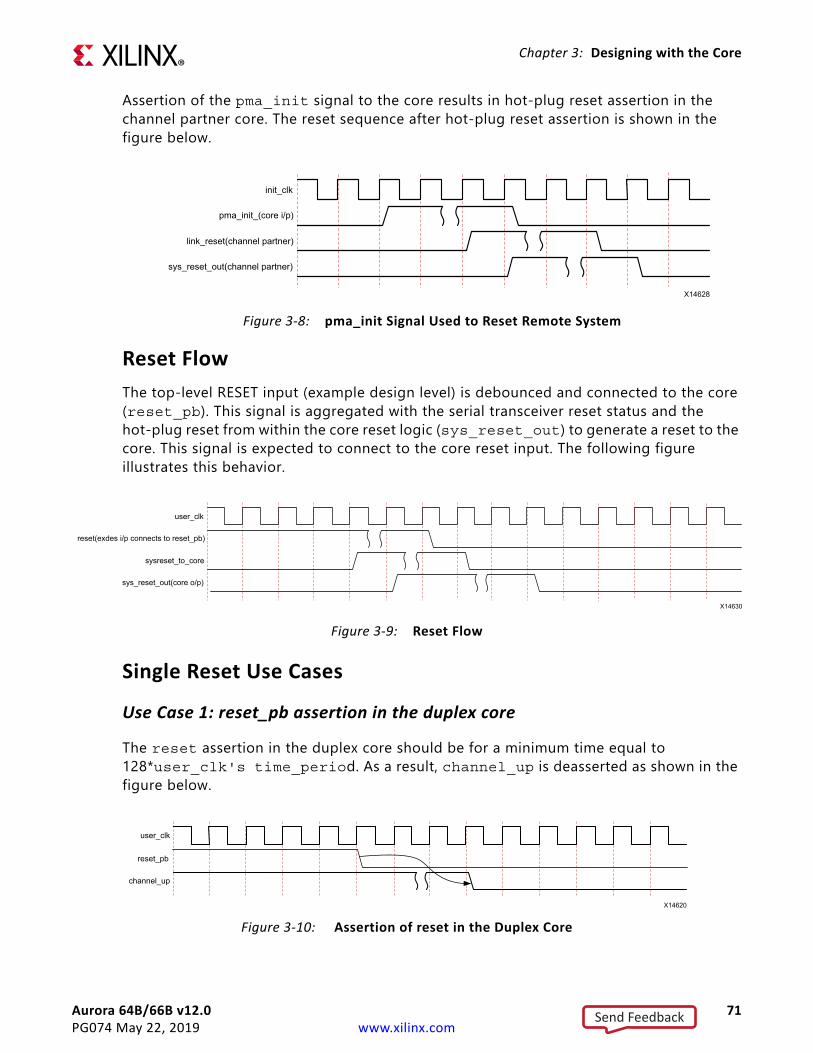
Aurora 64B/66B v12.0 71PG074 May 22, 2019 www.xilinx.com
Chapter 3: Designing with the Core
Assertion of the pma_init signal to the core results in hot-plug reset assertion in the channel partner core. The reset sequence after hot-plug reset assertion is shown in the figure below.
Reset FlowThe top-level RESET input (example design level) is debounced and connected to the core (reset_pb). This signal is aggregated with the serial transceiver reset status and the hot-plug reset from within the core reset logic (sys_reset_out) to generate a reset to the core. This signal is expected to connect to the core reset input. The following figure illustrates this behavior.
Single Reset Use Cases
Use Case 1: reset_pb assertion in the duplex core
The reset assertion in the duplex core should be for a minimum time equal to 128*user_clk's time_period. As a result, channel_up is deasserted as shown in the figure below.
X-Ref Target - Figure 3-8
Figure 3-8: pma_init Signal Used to Reset Remote System
link_reset(channel partner)
init_clk
X14628
sys_reset_out(channel partner)
pma_init_(core i/p)
X-Ref Target - Figure 3-9
Figure 3-9: Reset Flow
sysreset_to_core
user_clk
X14630
sys_reset_out(core o/p)
reset(exdes i/p connects to reset_pb)
X-Ref Target - Figure 3-10
Figure 3-10: Assertion of reset in the Duplex Core
reset_pb
channel_up
user_clk
X14620
Send Feedback
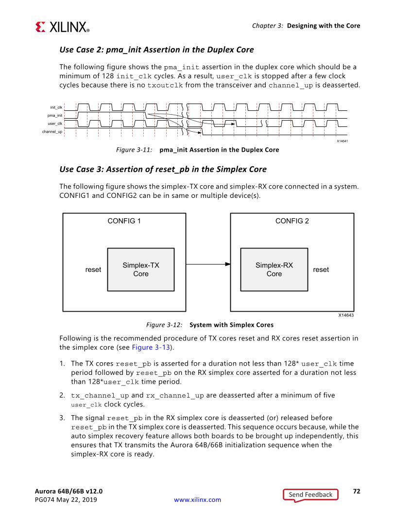
Aurora 64B/66B v12.0 72PG074 May 22, 2019 www.xilinx.com
Chapter 3: Designing with the Core
Use Case 2: pma_init Assertion in the Duplex Core
The following figure shows the pma_init assertion in the duplex core which should be a minimum of 128 init_clk cycles. As a result, user_clk is stopped after a few clock cycles because there is no txoutclk from the transceiver and channel_up is deasserted.
Use Case 3: Assertion of reset_pb in the Simplex Core
The following figure shows the simplex-TX core and simplex-RX core connected in a system. CONFIG1 and CONFIG2 can be in same or multiple device(s).
Following is the recommended procedure of TX cores reset and RX cores reset assertion in the simplex core (see Figure 3-13).
1. The TX cores reset_pb is asserted for a duration not less than 128* user_clk time period followed by reset_pb on the RX simplex core asserted for a duration not less than 128*user_clk time period.
2. tx_channel_up and rx_channel_up are deasserted after a minimum of five user_clk clock cycles.
3. The signal reset_pb in the RX simplex core is deasserted (or) released before reset_pb in the TX simplex core is deasserted. This sequence occurs because, while the auto simplex recovery feature allows both boards to be brought up independently, this ensures that TX transmits the Aurora 64B/66B initialization sequence when the simplex-RX core is ready.
X-Ref Target - Figure 3-11
Figure 3-11: pma_init Assertion in the Duplex Core
init_clk
pma_init
user_clk
channel_up
X14641
X-Ref Target - Figure 3-12
Figure 3-12: System with Simplex Cores
CONFIG 1
X14643
Simplex-TXCorereset
CONFIG 2
Simplex-RXCore reset
Send Feedback
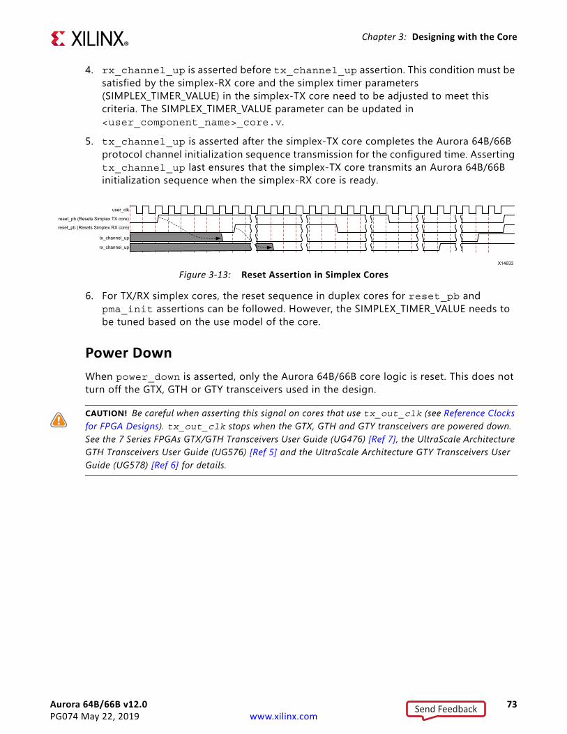
Aurora 64B/66B v12.0 73PG074 May 22, 2019 www.xilinx.com
Chapter 3: Designing with the Core
4. rx_channel_up is asserted before tx_channel_up assertion. This condition must be satisfied by the simplex-RX core and the simplex timer parameters (SIMPLEX_TIMER_VALUE) in the simplex-TX core need to be adjusted to meet this criteria. The SIMPLEX_TIMER_VALUE parameter can be updated in <user_component_name>_core.v.
5. tx_channel_up is asserted after the simplex-TX core completes the Aurora 64B/66B protocol channel initialization sequence transmission for the configured time. Asserting tx_channel_up last ensures that the simplex-TX core transmits an Aurora 64B/66B initialization sequence when the simplex-RX core is ready.
6. For TX/RX simplex cores, the reset sequence in duplex cores for reset_pb and pma_init assertions can be followed. However, the SIMPLEX_TIMER_VALUE needs to be tuned based on the use model of the core.
Power DownWhen power_down is asserted, only the Aurora 64B/66B core logic is reset. This does not turn off the GTX, GTH or GTY transceivers used in the design.
CAUTION! Be careful when asserting this signal on cores that use tx_out_clk (see Reference Clocks for FPGA Designs). tx_out_clk stops when the GTX, GTH and GTY transceivers are powered down. See the 7 Series FPGAs GTX/GTH Transceivers User Guide (UG476) [Ref 7], the UltraScale Architecture GTH Transceivers User Guide (UG576) [Ref 5] and the UltraScale Architecture GTY Transceivers User Guide (UG578) [Ref 6] for details.
X-Ref Target - Figure 3-13
Figure 3-13: Reset Assertion in Simplex Cores
user_clk
reset_pb (Resets Simplex TX core)
tx_channel_up
rx_channel_up
reset_pb (Resets Simplex RX core)
X14633
Send Feedback
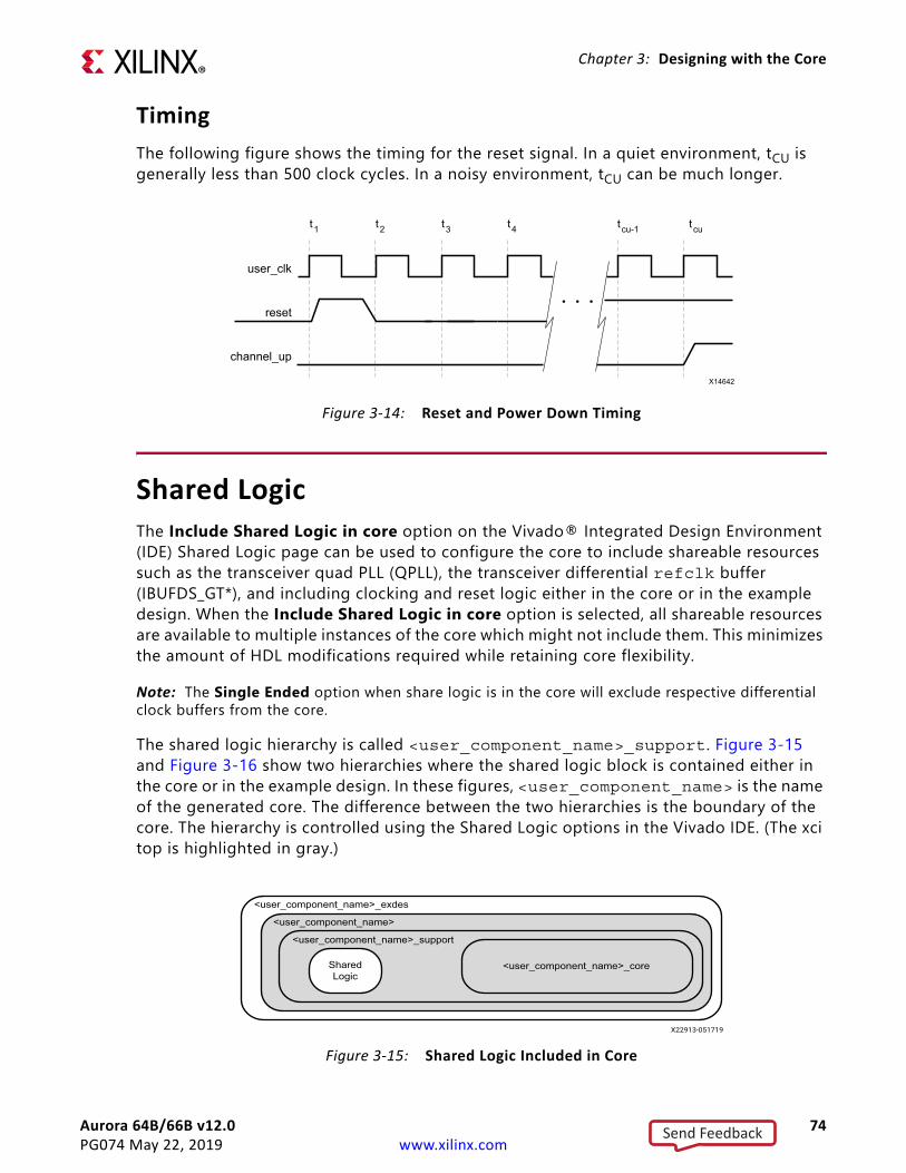
Aurora 64B/66B v12.0 74PG074 May 22, 2019 www.xilinx.com
Chapter 3: Designing with the Core
TimingThe following figure shows the timing for the reset signal. In a quiet environment, tCU is generally less than 500 clock cycles. In a noisy environment, tCU can be much longer.
Shared LogicThe Include Shared Logic in core option on the Vivado® Integrated Design Environment (IDE) Shared Logic page can be used to configure the core to include shareable resources such as the transceiver quad PLL (QPLL), the transceiver differential refclk buffer (IBUFDS_GT*), and including clocking and reset logic either in the core or in the example design. When the Include Shared Logic in core option is selected, all shareable resources are available to multiple instances of the core which might not include them. This minimizes the amount of HDL modifications required while retaining core flexibility.
Note: The Single Ended option when share logic is in the core will exclude respective differential clock buffers from the core.
The shared logic hierarchy is called <user_component_name>_support. Figure 3-15 and Figure 3-16 show two hierarchies where the shared logic block is contained either in the core or in the example design. In these figures, <user_component_name> is the name of the generated core. The difference between the two hierarchies is the boundary of the core. The hierarchy is controlled using the Shared Logic options in the Vivado IDE. (The xci top is highlighted in gray.)
X-Ref Target - Figure 3-14
Figure 3-14: Reset and Power Down Timing
X-Ref Target - Figure 3-15
Figure 3-15: Shared Logic Included in Core
user_clk
reset
channel_up
t1 t2 t3 t4 tcutcu-1
X14642
<user_component_name>_exdes
<user_component_name>
<user_component_name>_support
SharedLogic
<user_component_name>_core
Send Feedback
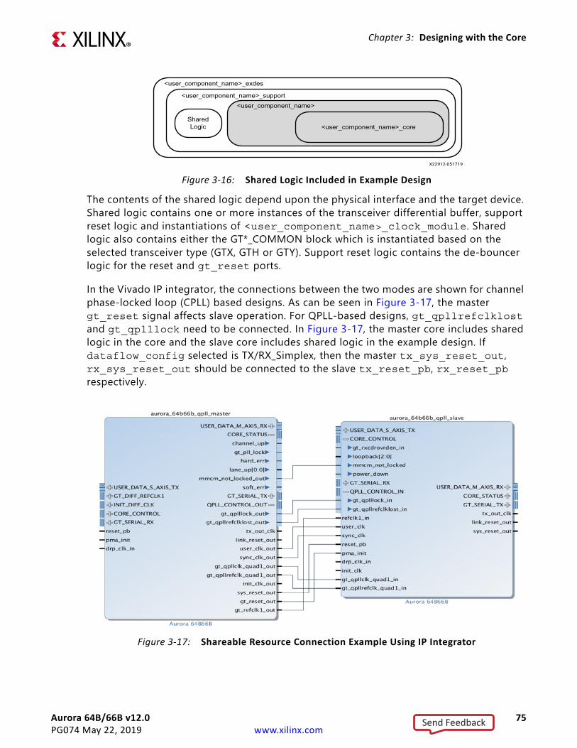
Aurora 64B/66B v12.0 75PG074 May 22, 2019 www.xilinx.com
Chapter 3: Designing with the Core
The contents of the shared logic depend upon the physical interface and the target device. Shared logic contains one or more instances of the transceiver differential buffer, support reset logic and instantiations of <user_component_name>_clock_module. Shared logic also contains either the GT*_COMMON block which is instantiated based on the selected transceiver type (GTX, GTH or GTY). Support reset logic contains the de-bouncer logic for the reset and gt_reset ports.
In the Vivado IP integrator, the connections between the two modes are shown for channel phase-locked loop (CPLL) based designs. As can be seen in Figure 3-17, the master gt_reset signal affects slave operation. For QPLL-based designs, gt_qpllrefclklost and gt_qplllock need to be connected. In Figure 3-17, the master core includes shared logic in the core and the slave core includes shared logic in the example design. If dataflow_config selected is TX/RX_Simplex, then the master tx_sys_reset_out, rx_sys_reset_out should be connected to the slave tx_reset_pb, rx_reset_pb respectively.
X-Ref Target - Figure 3-16
Figure 3-16: Shared Logic Included in Example Design
X-Ref Target - Figure 3-17
Figure 3-17: Shareable Resource Connection Example Using IP Integrator
<user_component_name>_exdes
<user_component_name>_support<user_component_name>
SharedLogic <user_component_name>_core
Send Feedback
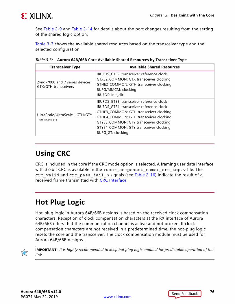
Aurora 64B/66B v12.0 76PG074 May 22, 2019 www.xilinx.com
Chapter 3: Designing with the Core
See Table 2-9 and Table 2-14 for details about the port changes resulting from the setting of the shared logic option.
Table 3-3 shows the available shared resources based on the transceiver type and the selected configuration.
Using CRCCRC is included in the core if the CRC mode option is selected. A framing user data interface with 32-bit CRC is available in the <user_component_name>_crc_top.v file. The crc_valid and crc_pass_fail_n signals (see Table 2-16) indicate the result of a received frame transmitted with CRC Interface.
Hot Plug LogicHot-plug logic in Aurora 64B/66B designs is based on the received clock compensation characters. Reception of clock compensation characters at the RX interface of Aurora 64B/66B infers that the communication channel is active and not broken. If clock compensation characters are not received in a predetermined time, the hot-plug logic resets the core and the transceiver. The clock compensation module must be used for Aurora 64B/66B designs.
IMPORTANT: It is highly recommended to keep hot plug logic enabled for predictable operation of the link.
Table 3-3: Aurora 64B/66B Core Available Shared Resources by Transceiver TypeTransceiver Type Available Shared Resources
Zynq-7000 and 7 series devices GTX/GTH transceivers
IBUFDS_GTE2: transceiver reference clockGTXE2_COMMON: GTX transceiver clockingGTHE2_COMMON: GTH transceiver clockingBUFG/MMCM: clockingIBUFDS: init_clk
UltraScale/UltraScale+ GTH/GTY Transceivers
IBUFDS_GTE3: transceiver reference clockIBUFDS_GTE4: transceiver reference clockGTHE3_COMMON: GTH transceiver clockingGTHE4_COMMON: GTH transceiver clockingGTYE3_COMMON: GTY transceiver clockingGTYE4_COMMON: GTY transceiver clockingBUFG_GT: clocking
Send Feedback
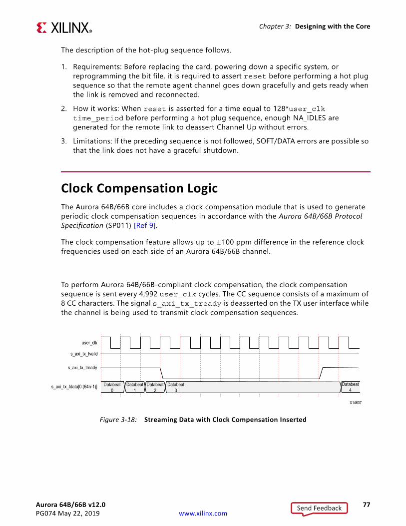
Aurora 64B/66B v12.0 77PG074 May 22, 2019 www.xilinx.com
Chapter 3: Designing with the Core
The description of the hot-plug sequence follows.
1. Requirements: Before replacing the card, powering down a specific system, or reprogramming the bit file, it is required to assert reset before performing a hot plug sequence so that the remote agent channel goes down gracefully and gets ready when the link is removed and reconnected.
2. How it works: When reset is asserted for a time equal to 128*user_clk time_period before performing a hot plug sequence, enough NA_IDLES are generated for the remote link to deassert Channel Up without errors.
3. Limitations: If the preceding sequence is not followed, SOFT/DATA errors are possible so that the link does not have a graceful shutdown.
Clock Compensation LogicThe Aurora 64B/66B core includes a clock compensation module that is used to generate periodic clock compensation sequences in accordance with the Aurora 64B/66B Protocol Specification (SP011) [Ref 9].
The clock compensation feature allows up to ±100 ppm difference in the reference clock frequencies used on each side of an Aurora 64B/66B channel.
To perform Aurora 64B/66B-compliant clock compensation, the clock compensation sequence is sent every 4,992 user_clk cycles. The CC sequence consists of a maximum of 8 CC characters. The signal s_axi_tx_tready is deasserted on the TX user interface while the channel is being used to transmit clock compensation sequences.
X-Ref Target - Figure 3-18
Figure 3-18: Streaming Data with Clock Compensation Inserted
s_axi_tx_tready
s_axi_tx_tdata[0:(64n-1)]
s_axi_tx_tvalid
X14637
Databeat 0
Databeat 4
user_clk
Databeat 1
Databeat 2
Databeat 3
Send Feedback
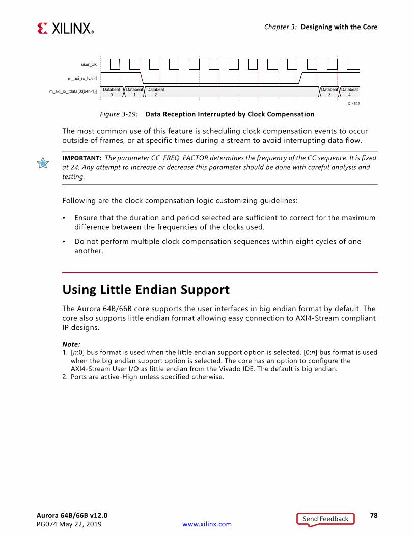
Aurora 64B/66B v12.0 78PG074 May 22, 2019 www.xilinx.com
Chapter 3: Designing with the Core
The most common use of this feature is scheduling clock compensation events to occur outside of frames, or at specific times during a stream to avoid interrupting data flow.
IMPORTANT: The parameter CC_FREQ_FACTOR determines the frequency of the CC sequence. It is fixed at 24. Any attempt to increase or decrease this parameter should be done with careful analysis and testing.
Following are the clock compensation logic customizing guidelines:
• Ensure that the duration and period selected are sufficient to correct for the maximum difference between the frequencies of the clocks used.
• Do not perform multiple clock compensation sequences within eight cycles of one another.
Using Little Endian SupportThe Aurora 64B/66B core supports the user interfaces in big endian format by default. The core also supports little endian format allowing easy connection to AXI4-Stream compliant IP designs.
Note:1. [n:0] bus format is used when the little endian support option is selected. [0:n] bus format is used
when the big endian support option is selected. The core has an option to configure theAXI4-Stream User I/O as little endian from the Vivado IDE. The default is big endian.
2. Ports are active-High unless specified otherwise.
X-Ref Target - Figure 3-19
Figure 3-19: Data Reception Interrupted by Clock Compensation
m_axi_rx_tvalid
m_axi_rx_tdata[0:(64n-1)]
user_clk
X14622
Databeat 0
Databeat 4
Databeat 2
Databeat 3
Databeat 1
Send Feedback
Aurora 64B/66B v12.0 79PG074 May 22, 2019 www.xilinx.com
Chapter 4
Design Flow StepsThis chapter describes customizing and generating the core, constraining the core, and the simulation, synthesis and implementation steps that are specific to this IP core. More detailed information about the standard Vivado® design flows and the IP integrator can be found in the following Vivado Design Suite user guides:
• Vivado Design Suite User Guide: Designing IP Subsystems using IP Integrator (UG994) [Ref 11]
• Vivado Design Suite User Guide: Designing with IP (UG896) [Ref 12]• Vivado Design Suite User Guide: Getting Started (UG910) [Ref 13]• Vivado Design Suite User Guide: Logic Simulation (UG900) [Ref 14]
Customizing and Generating the CoreThis section includes information about using Xilinx tools to customize and generate the core in the Vivado Design Suite.
When customizing and generating the core in the Vivado IP integrator, see the Vivado Design Suite User Guide: Designing IP Subsystems using IP Integrator (UG994) [Ref 11] for detailed information. The IP integrator might auto-compute certain configuration values when validating or generating the design. To check whether the values change, see the description of the parameter in this chapter. To view the parameter value, run the validate_bd_design command in the Tcl Console.
Use the following steps to customize the IP for use in your design by specifying values for the various parameters associated with the IP core:
1. Select the IP from the Vivado IP catalog (IP Catalog -> Aurora 64B66B).2. Double-click the selected IP or select Customize IP from the toolbar or right-click
menu.
For details, see the Vivado Design Suite User Guide: Designing with IP (UG896) [Ref 12] and the Vivado Design Suite User Guide: Getting Started (UG910) [Ref 13].
Send Feedback
Aurora 64B/66B v12.0 80PG074 May 22, 2019 www.xilinx.com
Chapter 4: Design Flow Steps
The Aurora 64B/66B core can be customized to suit a wide variety of requirements using the IP catalog. This chapter details the customization parameters and how these parameters are specified within the Vivado Integrated Design Environment (IDE).
Figure 4-1 through Figure 4-5 show the features described in the corresponding sections. The left side displays a representative block diagram of the Aurora 64B/66B core as currently configured. The right side consists of user-configurable parameters.
Figure 4-1 shows the Core Options tab of the Customize IP interface with the default options for Zynq®-7000 and 7 series devices.
Figure 4-2 shows the Core Options tab for UltraScale™ and UltraScale+ devices. Details on the customizing options are provided in the following subsections, starting with Component Name.
Note: Figures in this chapter are illustrations of the Vivado IDE. This layout depicted here might vary from the current version.
Send Feedback
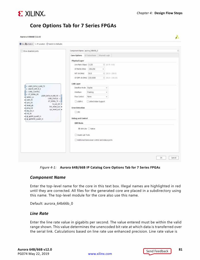
Aurora 64B/66B v12.0 81PG074 May 22, 2019 www.xilinx.com
Chapter 4: Design Flow Steps
Core Options Tab for 7 Series FPGAs
Component Name
Enter the top-level name for the core in this text box. Illegal names are highlighted in red until they are corrected. All files for the generated core are placed in a subdirectory using this name. The top-level module for the core also use this name.
Default: aurora_64b66b_0
Line Rate
Enter the line rate value in gigabits per second. The value entered must be within the valid range shown. This value determines the unencoded bit rate at which data is transferred over the serial link. Calculations based on line rate use enhanced precision. Line rate value is
X-Ref Target - Figure 4-1
Figure 4-1: Aurora 64B/66B IP Catalog Core Options Tab for 7 Series FPGAs
Send Feedback
Aurora 64B/66B v12.0 82PG074 May 22, 2019 www.xilinx.com
Chapter 4: Design Flow Steps
restricted to four decimal digits for UltraScale with the exception of 25.78125 Gb/s for GTY devices.
Default: 3.125 Gb/s for 7 series FPGA transceivers, 10.3125 Gb/s for UltraScale™ FPGA GTH and GTY transceivers and 25.78125 Gb/s for GTHE4/GTYE4 transceivers.
GT Reference Clock Frequency
Select a reference clock frequency in MHz from the list box which provides options based on the selected line rate. For best results, select the highest rate that can be practically applied to the reference clock input of the target device.
Default: 156.25 MHz
INIT clk (MHz)
Enter a valid INIT clock frequency in the text box.
Default: 50 MHz for 7 series FPGAs and Zynq® SoCs, line_rate/datapath_width for UltraScale™ and UltraScale+ devices.
GT DRP clk (MHz)
Enter a valid DRP clock frequency in the text box. Available only with 7 series FPGA transceivers.
Default: 100 MHz
Dataflow Mode
Select the options for the direction of the channel that the Aurora 64B/66B core supports. Simplex cores have a single, unidirectional serial port that connects to a complementary simplex core. Three simplex options are provided to select the channel direction supported by the core: RX-only_simplex, TX-only_simplex or TX/RX_simplex.
Duplex or TX/RX_simplex specify that the core has both TX and the corresponding RX communication channels.
Default: Duplex
Generate Aurora without GT
If this option is selected, then the Aurora core is generated without the GT that is available in the example design. This option is available only for UltraScale and UltraScale+ devices.
Send Feedback
Aurora 64B/66B v12.0 83PG074 May 22, 2019 www.xilinx.com
Chapter 4: Design Flow Steps
Interface
Select the type of datapath interface used for the core. Select Framing to use a complete AXI4-Stream interface that allows encapsulation of data frames of any length. Select Streaming to use a simple AXI4-Stream interface to stream data through the Aurora 64B/66B channel.
Default: Framing
Flow Control
Select the required option to add flow control to the core. User flow control (UFC) allows applications to send each other brief, high-priority messages through the Aurora 64B/66B channel. Native flow control (NFC) allows full-duplex receivers to regulate the rate of the data sent to them. Immediate mode allows idle codes to be inserted within data frames while completion mode only inserts idle codes between complete data frames.
Available options are:
• None • UFC only• Immediate NFC• Completion NFC• UFC + Immediate NFC • UFC + Completion NFC
For the streaming interface, only immediate mode is available. For the framing interface, both immediate and completion modes are available.
Default: None
USER K
Select to add a USER K interface to the core. USER-K blocks are special single-block codes passed directly to the user application. These blocks are used to implement application-specific control functions.
Default: Unchecked
Little Endian Support
Select to change all of the interface(s) to little endian format. See Using Little Endian Support in Chapter 3 for more information, By default the core uses big endian format.
Default: Unchecked
Send Feedback
Aurora 64B/66B v12.0 84PG074 May 22, 2019 www.xilinx.com
Chapter 4: Design Flow Steps
CRC
Select the option to insert CRC32 in the data stream.
Default: Unchecked
DRP Mode
Select the required interface to control or monitor the transceiver interface using the DRP.
Available options are:
• Native• AXI4_Lite
Default: AXI4_Lite
Vivado Lab Tools
Select to add Vivado lab tools to the Aurora 64B/66B core. (See Using Vivado Lab Tools.) This option provides a debugging interface that shows the core status signals.
Default: Unchecked
Additional Transceiver Control and Status Ports
Select to include transceiver control and status ports in core top level.
Default: Unchecked
Send Feedback
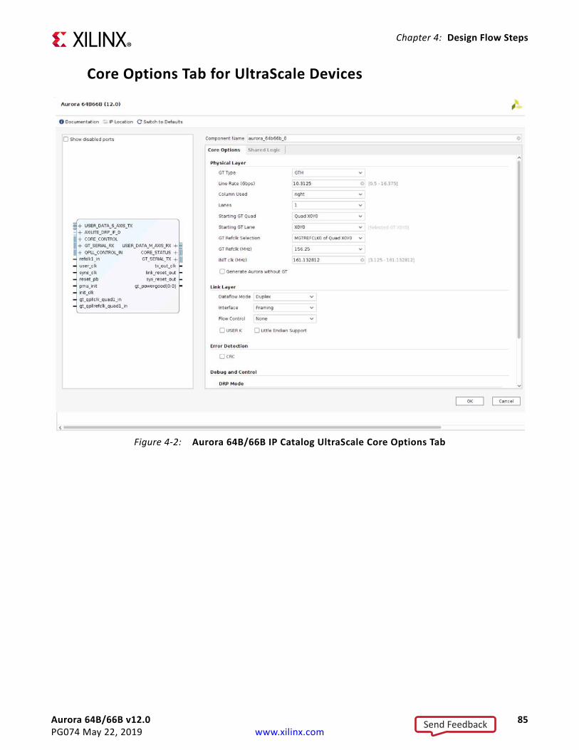
Aurora 64B/66B v12.0 85PG074 May 22, 2019 www.xilinx.com
Chapter 4: Design Flow Steps
Core Options Tab for UltraScale DevicesX-Ref Target - Figure 4-2
Figure 4-2: Aurora 64B/66B IP Catalog UltraScale Core Options Tab
Send Feedback
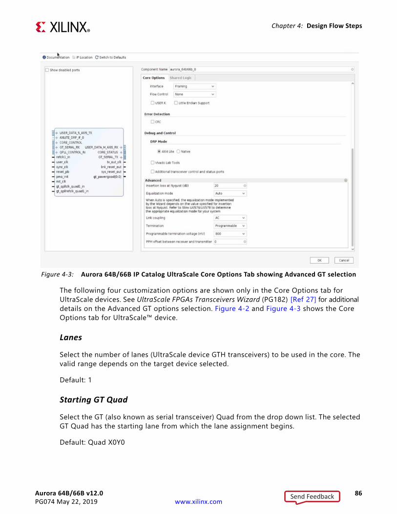
Aurora 64B/66B v12.0 86PG074 May 22, 2019 www.xilinx.com
Chapter 4: Design Flow Steps
The following four customization options are shown only in the Core Options tab for UltraScale devices. See UltraScale FPGAs Transceivers Wizard (PG182) [Ref 27] for additional details on the Advanced GT options selection. Figure 4-2 and Figure 4-3 shows the Core Options tab for UltraScale™ device.
Lanes
Select the number of lanes (UltraScale device GTH transceivers) to be used in the core. The valid range depends on the target device selected.
Default: 1
Starting GT Quad
Select the GT (also known as serial transceiver) Quad from the drop down list. The selected GT Quad has the starting lane from which the lane assignment begins.
Default: Quad X0Y0
X-Ref Target - Figure 4-3
Figure 4-3: Aurora 64B/66B IP Catalog UltraScale Core Options Tab showing Advanced GT selection
Send Feedback
Aurora 64B/66B v12.0 87PG074 May 22, 2019 www.xilinx.com
Chapter 4: Design Flow Steps
GT Type
Select the GT transceiver type from the drop-down menu. The options provided are GTH and GTY.
Default: GTH
Starting GT Lane
Select the starting lane of the core from the drop-down list that is generated based on the selected GT Quad. With Lanes, Starting GT Quad and Starting GT lane, the core gets generated with a consecutive number of lanes.
Default: X0Y0
Note: Channel bonding across SLR boundaries is not supported by the core and restricted from the Vivado IDE.
GT Refclk Selection
Select reference clock sources for the UltraScale transceivers from the drop-down list.
Default: MGTREFCLK0 of Quad X0Y0
CAUTION! For GTY core configuration and line rate > 16.375G, the GT Refclk selection option will not be available. The Aurora 64b66b core will default to active transceiver Quads GTREFCLK. Each Quads GT Refclk should be individually fed. For more details, see the UltraScale Architecture GTY Transceivers User Guide (UG578) [Ref 6].
Send Feedback
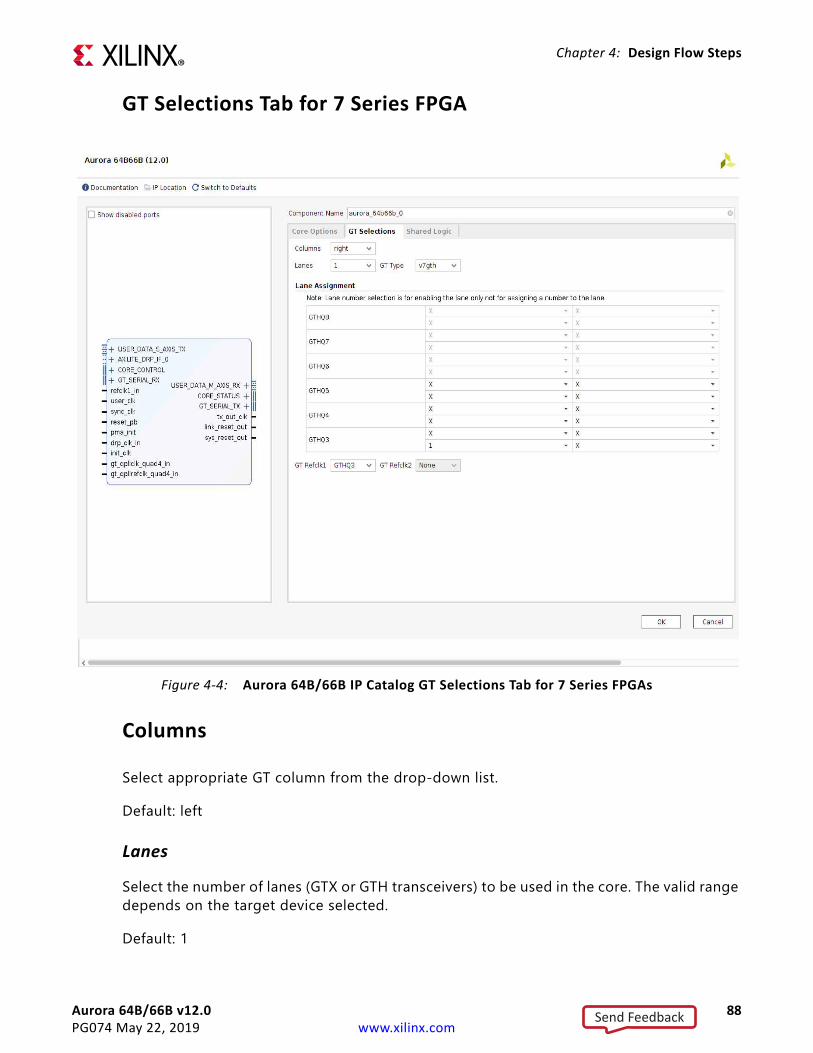
Aurora 64B/66B v12.0 88PG074 May 22, 2019 www.xilinx.com
Chapter 4: Design Flow Steps
GT Selections Tab for 7 Series FPGA
Columns
Select appropriate GT column from the drop-down list.
Default: left
Lanes
Select the number of lanes (GTX or GTH transceivers) to be used in the core. The valid range depends on the target device selected.
Default: 1
X-Ref Target - Figure 4-4
Figure 4-4: Aurora 64B/66B IP Catalog GT Selections Tab for 7 Series FPGAs
Send Feedback
Aurora 64B/66B v12.0 89PG074 May 22, 2019 www.xilinx.com
Chapter 4: Design Flow Steps
GT_TYPE
Select the type of serial transceiver from the drop-down list. This option is applicable only for Virtex®-7 XT devices. For other devices, the drop-down box is not visible.
Available options are:
• gtx• v7gth
Default: gtx
Lane Assignment
See the diagram in the information area in Figure 4-4. Each numbered row represents a serial transceiver tile and each active box represents an available GTX or GTH transceiver. For each Aurora 64B/66B lane in the core, starting with Lane 1, select a GTX or GTH transceiver and place the lane by selecting its number in the GTX or GTH transceiver placement box.
• X in the drop-down menu means that lane is not selected.• <1—16> selected from the drop-down menu means that particular lane is selected. It
does not assign that number to the physical lane.
RECOMMENDED: Always select consecutive/physically adjacent lanes for a multi-GT design.
Note: The core generates transceiver placement (LOC) constraints in ascending fashion. Move the cursor in the Vivado IDE to see the transceiver being selected in the 7 series and Zynq®-7000 family-based design. Lane numbering serves only to enable the lanes and not to assign numbers to the lanes. The Lane Assignment is not available for UltraScale architecture-based designs. It is strongly recommended that lane selection should be continuous for timing closure.
GT REFCLK1 and GT REFCLK2
Select reference clock sources for the GTX and GTH transceiver tiles from the drop-down list in this section.
Default: GT REFCLK Source 1: GTXQn/ GTHQn; GT REFCLK Source 2: None;
Note: n depends on the serial transceiver (GTX or GTH) position.
Send Feedback
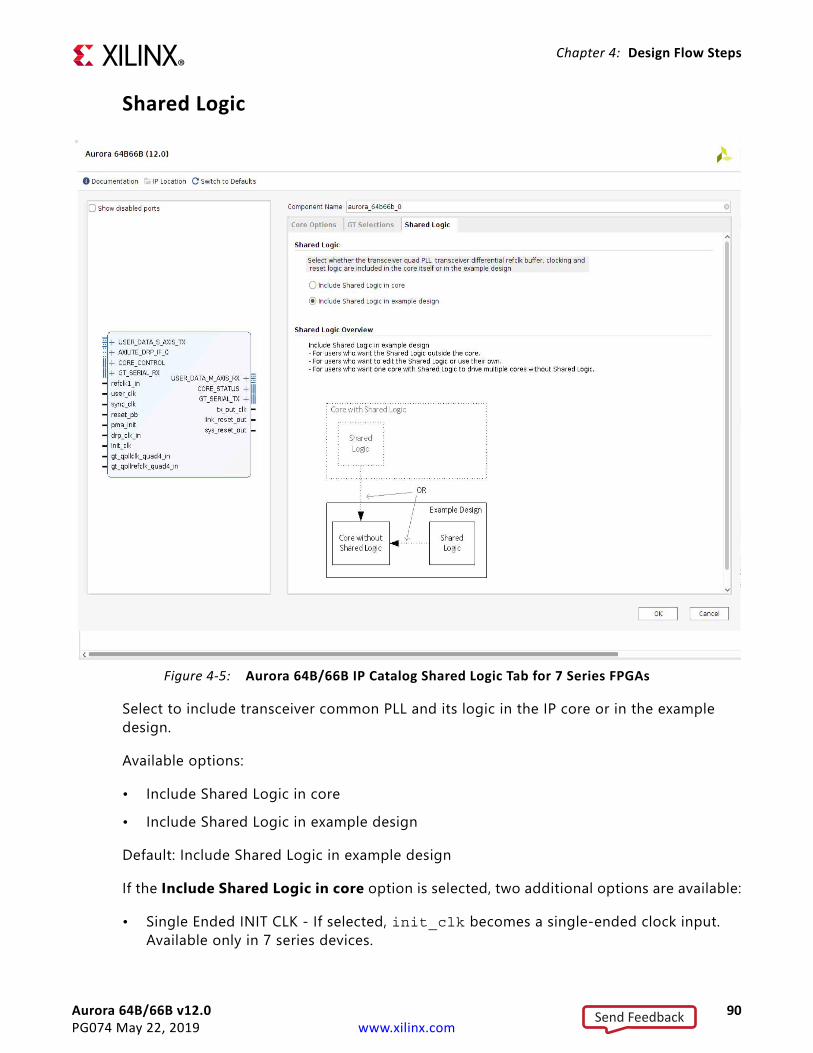
Aurora 64B/66B v12.0 90PG074 May 22, 2019 www.xilinx.com
Chapter 4: Design Flow Steps
Shared Logic
Select to include transceiver common PLL and its logic in the IP core or in the example design.
Available options:
• Include Shared Logic in core • Include Shared Logic in example design
Default: Include Shared Logic in example design
If the Include Shared Logic in core option is selected, two additional options are available:
• Single Ended INIT CLK - If selected, init_clk becomes a single-ended clock input. Available only in 7 series devices.
X-Ref Target - Figure 4-5
Figure 4-5: Aurora 64B/66B IP Catalog Shared Logic Tab for 7 Series FPGAs
Send Feedback
Aurora 64B/66B v12.0 91PG074 May 22, 2019 www.xilinx.com
Chapter 4: Design Flow Steps
• Single Ended GTREF CLK - If selected, the GT reference clock becomes a single-ended clock input.
Click OK to generate the core. (See Generating the Core with Quick Start.) The modules for the Aurora 64B/66B core are written to the IP catalog tool project directory using the same name as the top level of the core.
Notes: 1. In the IP integrator the core gives the expected frequency values in long format as per the IP integrator guidelines;
however, internally the precision is the same as shown in Vivado IDE. 2. In the IP integrator the clock and reset ports are grouped into the single-clock port and single-reset port interfaces
respectively. Data and AXI4-Stream flow control ports are grouped into AXI4-Stream interfaces. The other input and output ports are grouped into display interfaces.
3. For the ports grouped in display interfaces the connections need to be made port-to-port.4. The non-AXI UFC ports are listed below the UFC interfaces. 5. Based on the configuration chosen, the expected frequency values are shown for the clock inputs to the core.
User ParametersTable 4-1 shows the relationship between the fields in the Vivado IDE and the User Parameters in the XCI files (which can be viewed in the Tcl Console). Use the information in the tables for batch-driven Tcl flows to set Vivado IDE parameters and generate the Aurora 64B/66B core.
Table 4-1: Vivado IDE Parameter to User Parameter Mapping(1)
Vivado IDE Parameter User Parameter Default Value(1)
Core OptionsPhysical Layer
Line Rate (Gb/s) C_LINE_RATE 3.125/10.3125
GT Type(11) C_GT_TYPE GTH/GTYColumn Used(11) C_UCOLUMN_USED rightStarting GT Quad(11) C_START_QUAD Quad X0Y0Starting GT Lane(11) C_START_Lane X0Y0
GT Refclk Selection(13) C_REFCLK_SOURCE MGTREFCLK0 of Quad X0Y0
GT Refclk (MHz)(15) C_REFCLK_FREQUENCY 156.250
INIT clk (MHz) C_INIT_CLK 50.0/161.1328125
GT DRP clk (MHz)(9) DRP_FREQ 100.0000Generate Aurora without GT(14) C_GTWIZ_OUT false
Link LayerDataflow Mode Dataflow_Config Duplex
Send Feedback
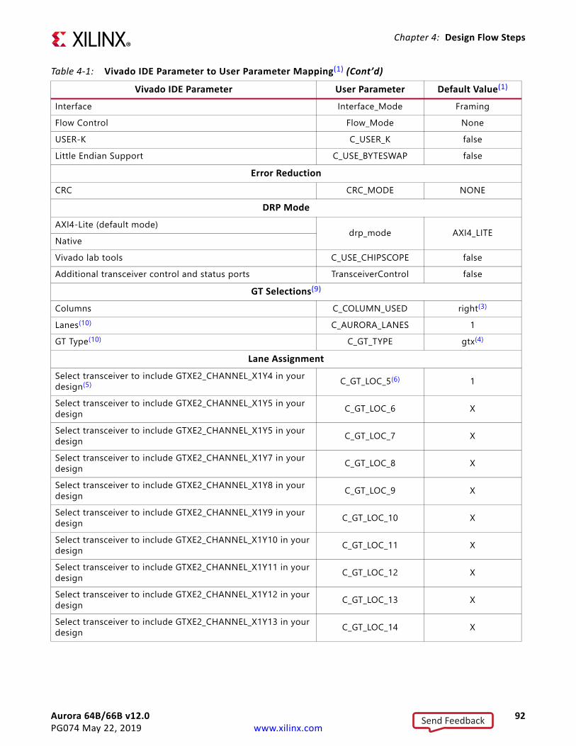
Aurora 64B/66B v12.0 92PG074 May 22, 2019 www.xilinx.com
Chapter 4: Design Flow Steps
Interface Interface_Mode FramingFlow Control Flow_Mode NoneUSER-K C_USER_K falseLittle Endian Support C_USE_BYTESWAP false
Error ReductionCRC CRC_MODE NONE
DRP ModeAXI4-Lite (default mode)
drp_mode AXI4_LITENativeVivado lab tools C_USE_CHIPSCOPE falseAdditional transceiver control and status ports TransceiverControl false
GT Selections(9)
Columns C_COLUMN_USED right(3)
Lanes(10) C_AURORA_LANES 1GT Type(10) C_GT_TYPE gtx(4)
Lane AssignmentSelect transceiver to include GTXE2_CHANNEL_X1Y4 in your design(5) C_GT_LOC_5(6) 1
Select transceiver to include GTXE2_CHANNEL_X1Y5 in your design C_GT_LOC_6 X
Select transceiver to include GTXE2_CHANNEL_X1Y5 in your design C_GT_LOC_7 X
Select transceiver to include GTXE2_CHANNEL_X1Y7 in your design C_GT_LOC_8 X
Select transceiver to include GTXE2_CHANNEL_X1Y8 in your design C_GT_LOC_9 X
Select transceiver to include GTXE2_CHANNEL_X1Y9 in your design C_GT_LOC_10 X
Select transceiver to include GTXE2_CHANNEL_X1Y10 in your design C_GT_LOC_11 X
Select transceiver to include GTXE2_CHANNEL_X1Y11 in your design C_GT_LOC_12 X
Select transceiver to include GTXE2_CHANNEL_X1Y12 in your design C_GT_LOC_13 X
Select transceiver to include GTXE2_CHANNEL_X1Y13 in your design C_GT_LOC_14 X
Table 4-1: Vivado IDE Parameter to User Parameter Mapping(1) (Cont’d)
Vivado IDE Parameter User Parameter Default Value(1)
Send Feedback
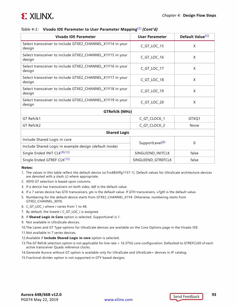
Aurora 64B/66B v12.0 93PG074 May 22, 2019 www.xilinx.com
Chapter 4: Design Flow Steps
Select transceiver to include GTXE2_CHANNEL_X1Y14 in your design C_GT_LOC_15 X
Select transceiver to include GTXE2_CHANNEL_X1Y15 in your design C_GT_LOC_16 X
Select transceiver to include GTXE2_CHANNEL_X1Y16 in your design C_GT_LOC_17 X
Select transceiver to include GTXE2_CHANNEL_X1Y17 in your design C_GT_LOC_18 X
Select transceiver to include GTXE2_CHANNEL_X1Y18 in your design C_GT_LOC_19 X
Select transceiver to include GTXE2_CHANNEL_X1Y19 in your design C_GT_LOC_20 X
GTRefclk (MHz)GT Refclk1 C_GT_CLOCK_1 GTXQ1GT Refclk2 C_GT_CLOCK_2 None
Shared LogicInclude Shared Logic in core
SupportLevel(8) 0Include Shared Logic in example design (default mode)Single Ended INIT CLK(9)(12) SINGLEEND_INITCLK falseSingle Ended GTREF CLK(12) SINGLEEND_GTREFCLK false
Notes: 1. The values in this table reflect the default device (xc7vx485tffg1157-1). Default values for UltraScale architecture devices
are denoted with a slash (/) where appropriate.2. X0Y0 GT selection is based upon columns.3. If a device has transceivers on both sides, left is the default value.4. If a 7 series device has GTX transceivers, gtx is the default value. If GTH transceivers, v7gth is the default value.5. Numbering for the default device starts from GTXE2_CHANNEL_X1Y4. Otherwise, numbering starts from
GTXE2_CHANNEL_X0Y0.6. C_GT_LOC_i where i varies from 1 to 48.7. By default, the lowest i C_GT_LOC_i is assigned.8. If Shared Logic in Core option is selected, SupportLevel is 1.9. Not available in UltraScale devices.10.The Lanes and GT Type options for UltraScale devices are available on the Core Options page in the Vivado IDE.11.Not available in 7 series devices.12.Available if Include Shared Logic in core option is selected.13.The GT Refclk selection option is not applicable for line rate > 16.375G core configuration. Defaulted to GTREFCLK0 of each
active transceiver Quads reference clocks. 14.Generate Aurora without GT option is available only for UltraScale and UltraScale+ devices in IP catalog.15.Fractional divider option is not supported in GTY based designs.
Table 4-1: Vivado IDE Parameter to User Parameter Mapping(1) (Cont’d)
Vivado IDE Parameter User Parameter Default Value(1)
Send Feedback
Aurora 64B/66B v12.0 94PG074 May 22, 2019 www.xilinx.com
Chapter 4: Design Flow Steps
RECOMMENDED: Do not alter any default locations, unless otherwise absolutely needed after the design is generated, or else the design functionality cannot be guaranteed.
RECOMMENDED: For UltraScale and UltraScale+ devices based designs when a line rate of less than 8.0 Gb/s is chosen, the CPLL becomes part of the GT Wizard hierarchical core.
Output GenerationThe customized Aurora 64B/66B core is delivered as a set of HDL source modules in Verilog. These files are arranged in a predetermined directory structure under the project directory name provided to the IP catalog when the project is created. For details, see the Vivado Design Suite User Guide: Designing with IP (UG896) [Ref 12].
Managing Shared Logic FilesYou can preview the shared logic files when you select Shared Logic in Example Design. You can see this option in IP Sources tab in the Vivado Project Manager along with Synthesis, Simulation filesets, a new fileset for Shared Logic Files. These are read only files which can be optionally copied in to the project if you want to use them as part of the project. You can use these files directly instead of taking the additional step of opening example design and then using these additional files. In the IP sources tab, you can right click the Aurora IP which was configured as Shared Logic in Example Design, and then select the Copy Shared Logic into Project option to copy these files in to the project hierarchy view.
CAUTION! You are cautioned that these shared logic files are read only and when copying them into project view, an additional copy of the same is generated and the ownership is transferred to the project. While using these files, make sure to follow all the sharing guidelines as per the transceiver type.
Send Feedback
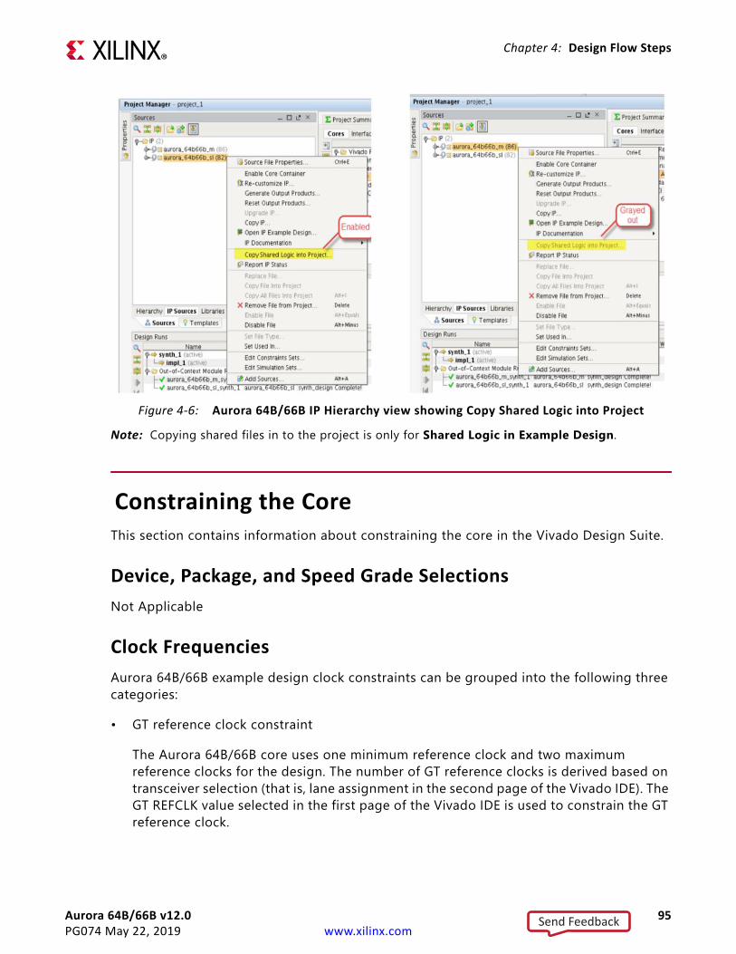
Aurora 64B/66B v12.0 95PG074 May 22, 2019 www.xilinx.com
Chapter 4: Design Flow Steps
Note: Copying shared files in to the project is only for Shared Logic in Example Design.
Constraining the CoreThis section contains information about constraining the core in the Vivado Design Suite.
Device, Package, and Speed Grade SelectionsNot Applicable
Clock FrequenciesAurora 64B/66B example design clock constraints can be grouped into the following three categories:
• GT reference clock constraint
The Aurora 64B/66B core uses one minimum reference clock and two maximum reference clocks for the design. The number of GT reference clocks is derived based on transceiver selection (that is, lane assignment in the second page of the Vivado IDE). The GT REFCLK value selected in the first page of the Vivado IDE is used to constrain the GT reference clock.
X-Ref Target - Figure 4-6
Figure 4-6: Aurora 64B/66B IP Hierarchy view showing Copy Shared Logic into Project
Send Feedback
Aurora 64B/66B v12.0 96PG074 May 22, 2019 www.xilinx.com
Chapter 4: Design Flow Steps
Note: The GT reference clock location constraint should be added to the <user_component_name>_example.xdc file.
• CORECLK clock constraint
CORECLKs are the clock signals on which the core functions. CORECLKs such as USER_CLK and SYNC_CLK are derived from the TXOUTCLK signal from the master lane. The master lane is the selected lane itself if it is a single lane configuration. In case of multi-lane configuration, it is chosen from the middle lane amongst the number of lanes configured. For example, a seven lane design would have the middle lane as the third lane (TXOUTCLK[3]). The Aurora 64B/66B core calculates the USER_CLK/SYNC_CLK frequency based on the line rate and transceiver interface width. The create_clock XDC command is used to constrain all CORECLKs.
• INIT CLK constraint
The Aurora 64B/66B example design uses a debounce circuit to sample PMA_INIT asynchronously clocked by the init_clk clock. The create_clock XDC command is used to constrain the init_clk clock. The init_clk frequency value in Vivado IDE is restricted to six decimal places.
RECOMMENDED: It is recommended to have the system clock frequency lower than the transceiver reference clock frequency and in the range of 50 to 200 MHz for 7 series and Zynq devices. For UltraScale devices, the recommended range is 6.25 MHz to line_rate/64 or 200 MHz whichever is less.See UltraScale Architecture GTH Transceivers User Guide (UG576) [Ref 5] and UltraScale Architecture GTY Transceivers User Guide (UG578) [Ref 6] for more information on valid use models for the free running system clock (init_clk).
Clock ManagementNot Applicable
Clock PlacementNot Applicable
BankingNot Applicable
Transceiver PlacementThe set_property XDC command is used to constrain the transceiver location. This is provided as a tooltip on the GT Selections tab of the Vivado IDE. A sample XDC is provided for reference.
Send Feedback
Aurora 64B/66B v12.0 97PG074 May 22, 2019 www.xilinx.com
Chapter 4: Design Flow Steps
I/O Standard and PlacementThe positive differential clock input pin (ends with _P) and negative differential clock input pin (ends with _N) are used as the transceiver reference clock. The set_property XDC command is used to constrain the transceiver reference clock pins.
False Paths
The False Path constraint is defined on the first stage of the flip-flop of the clock domain crossing (CDC) module.
Example Design
The generated example design including support logic has a 3.125 Gb/s line rate and a 156.25 MHz reference clock. The XDC file generated for xc7vx485tffg1157-1, the default device, follows:
################################ CLOCK CONSTRAINTS ##########################User Clock Constraint: the value is selected based on the line rate of the module#create_clock -period 20.48 [get_pins
aurora_64b66b_0_block_i/clock_module_i/user_clk_net_i/I]
# SYNC Clock Constraint#create_clock -period 10.240 [get_pins
aurora_64b66b_0_block_i/clock_module_i/sync_clock_net_i/I]
################################ IP LEVEL CONSTRAINTS START ################# Following constraints present in aurora_64b66b_0.xdc# Create clock constraint for TXOUTCLK from GT#create_clock -period 10.240 [get_pins -hier -filter
{name=~*aurora_64b66b_0_wrapper_i*aurora_64b66b_0_multi_gt_i*aurora_64b66b_0_gtx_inst/gtxe2_i/TXOUTCLK}]# Create clock constraint for RXOUTCLK from GT#create_clock -period 10.240 [get_pins -hier -filter
{name=~*aurora_64b66b_0_wrapper_i*aurora_64b66b_0_multi_gt_i*aurora_64b66b_0_gtx_inst/gtxe2_i/RXOUTCLK}]################################ IP LEVEL CONSTRAINTS END ################### Reference clock constraint for GTXcreate_clock -period 6.400 [get_ports GTXQ1_P]
### DRP Clock Constraintcreate_clock -period 10.000 [get_ports DRP_CLK_IN]
# 50MHz board Clock Constraintcreate_clock -period 20.000 [get_ports INIT_CLK_P]
###### No cross clock domain analysis. Domains are not related ################ set_false_path -from [get_clocks init_clk] -to [get_clocks user_clk]## set_false_path -from [get_clocks user_clk] -to [get_clocks init_clk]## set_false_path -from [get_clocks init_clk] -to [get_clocks sync_clk]## set_false_path -from [get_clocks sync_clk] -to [get_clocks init_clk]
## ## set_false_path -from init_clk -to [get_clocks -of_objects [get_pins aurora_64b66b_0_block_i/clock_module_i/mmcm_adv_inst/CLKOUT0]]##
Send Feedback
Aurora 64B/66B v12.0 98PG074 May 22, 2019 www.xilinx.com
Chapter 4: Design Flow Steps
## ## set_false_path -from [get_clocks -of_objects [get_pins aurora_64b66b_0_block_i/clock_module_i/mmcm_adv_inst/CLKOUT0]] -to init_clk#### ## set_false_path -from init_clk -to [get_clocks -of_objects [get_pins
aurora_64b66b_0_block_i/clock_module_i/mmcm_adv_inst/CLKOUT1]]#### ## set_false_path -from [get_clocks -of_objects [get_pins
aurora_64b66b_0_block_i/clock_module_i/mmcm_adv_inst/CLKOUT1]] -to init_clk#### ## set_false_path -from [get_clocks -of_objects [get_pins
aurora_64b66b_0_block_i/clock_module_i/initclk_bufg_i/O]] -to [get_clocks -of_objects [get_pins -hier -filter {name=~*aurora_64b66b_0_i*inst*aurora_64b66b_0_wrapper_i*aurora_64b66b_0_multi_gt_i*aurora_64b66b_0_gtx_inst/gtxe2_i/RXOUTCLK}]]#### ## set_false_path -from [get_clocks -of_objects [get_pins -hier -filter
{name=~*aurora_64b66b_0_i*inst*aurora_64b66b_0_wrapper_i*aurora_64b66b_0_multi_gt_i*aurora_64b66b_0_gtx_inst/gtxe2_i/RXOUTCLK}]] -to [get_clocks -of_objects [get_pins aurora_64b66b_0_block_i/clock_module_i/initclk_bufg_i/O]]#### ## set_false_path -from [get_clocks -of_objects [get_pins -hier -filter
{name=~*aurora_64b66b_0_i*inst*aurora_64b66b_0_wrapper_i*aurora_64b66b_0_multi_gt_i*aurora_64b66b_0_gtx_inst/gtxe2_i/RXOUTCLK}]] -to [get_clocks -of_objects [get_pins aurora_64b66b_0_block_i/clock_module_i/mmcm_adv_inst/CLKOUT0]]#### ## set_false_path -from [get_clocks -of_objects [get_pins
aurora_64b66b_0_block_i/clock_module_i/mmcm_adv_inst/CLKOUT0]] -to [get_clocks -of_objects [get_pins -hier -filter {name=~*aurora_64b66b_0_i*inst*aurora_64b66b_0_wrapper_i*aurora_64b66b_0_multi_gt_i*aurora_64b66b_0_gtx_inst/gtxe2_i/RXOUTCLK}]]
## GT CLOCK Locations ### Differential SMA Clock Connectionset_property LOC AH6 [get_ports GTXQ1_P]set_property LOC AH5 [get_ports GTXQ1_N]
set_property LOC GTXE2_CHANNEL_X1Y4 [get_cells aurora_64b66b_0_block_i/aurora_64b66b_0_i/inst/aurora_64b66b_0_wrapper_i/aurora_64b66b_0_multi_gt_i/aurora_64b66b_0_gtx_inst/gtxe2_i]
# false path constraints to the example design logic set_false_path -to [get_pins -hier *aurora_64b66b_0_cdc_to*/D]
##################################################################################################### ##Note: User should add LOC based upon the board # Below LOC's are place holders and need to be changed as per the device and board #set_property LOC D17 [get_ports INIT_CLK_P] #set_property LOC D18 [get_ports INIT_CLK_N] #set_property LOC G19 [get_ports RESET] #set_property LOC K18 [get_ports PMA_INIT] #set_property LOC A20 [get_ports CHANNEL_UP] #set_property LOC A17 [get_ports LANE_UP] #set_property LOC Y15 [get_ports HARD_ERR] #set_property LOC AH10 [get_ports SOFT_ERR]
Send Feedback
Aurora 64B/66B v12.0 99PG074 May 22, 2019 www.xilinx.com
Chapter 4: Design Flow Steps
#set_property LOC AD16 [get_ports DATA_ERR_COUNT[0]] #set_property LOC Y19 [get_ports DATA_ERR_COUNT[1]] #set_property LOC Y18 [get_ports DATA_ERR_COUNT[2]] #set_property LOC AA18 [get_ports DATA_ERR_COUNT[3]] #set_property LOC AB18 [get_ports DATA_ERR_COUNT[4]] #set_property LOC AB19 [get_ports DATA_ERR_COUNT[5]] #set_property LOC AC19 [get_ports DATA_ERR_COUNT[6]] #set_property LOC AB17 [get_ports DATA_ERR_COUNT[7]] #set_property LOC AG29 [get_ports DRP_CLK_IN] #// DRP CLK needs a clock LOC ##Note: User should add IOSTANDARD based upon the board # Below IOSTANDARDs are place holders and need to be changed as per the device and board #set_property IOSTANDARD DIFF_HSTL_II_18 [get_ports INIT_CLK_P] #set_property IOSTANDARD DIFF_HSTL_II_18 [get_ports INIT_CLK_N] #set_property IOSTANDARD LVCMOS18 [get_ports RESET] #set_property IOSTANDARD LVCMOS18 [get_ports PMA_INIT] #set_property IOSTANDARD LVCMOS18 [get_ports CHANNEL_UP] #set_property IOSTANDARD LVCMOS18 [get_ports LANE_UP] #set_property IOSTANDARD LVCMOS18 [get_ports HARD_ERR] #set_property IOSTANDARD LVCMOS18 [get_ports SOFT_ERR] #set_property IOSTANDARD LVCMOS18 [get_ports DATA_ERR_COUNT[0]] #set_property IOSTANDARD LVCMOS18 [get_ports DATA_ERR_COUNT[1]] #set_property IOSTANDARD LVCMOS18 [get_ports DATA_ERR_COUNT[2]] #set_property IOSTANDARD LVCMOS18 [get_ports DATA_ERR_COUNT[3]] #set_property IOSTANDARD LVCMOS18 [get_ports DATA_ERR_COUNT[4]] #set_property IOSTANDARD LVCMOS18 [get_ports DATA_ERR_COUNT[5]] #set_property IOSTANDARD LVCMOS18 [get_ports DATA_ERR_COUNT[6]] #set_property IOSTANDARD LVCMOS18 [get_ports DATA_ERR_COUNT[7]] #set_property IOSTANDARD LVCMOS18 [get_ports DRP_CLK_IN] #// DRP CLK needs a clock IOSTDLOC
The preceding example XDC is for reference only. This XDC is created automatically when the core is generated from the Vivado design tools.
SimulationFor comprehensive information about Vivado simulation components, as well as information about using supported third-party tools, see the Vivado Design Suite User Guide: Logic Simulation (UG900) [Ref 14].
IMPORTANT: For cores targeting 7 series, Zynq-7000, UltraScale and UltraScale+ devices, UNIFAST libraries are not supported. Xilinx IP is tested and qualified with UNISIM libraries only.
The Aurora 64B/66B core provides a demonstration test bench for the example design. Simulation status is reported through messages. The TEST COMPLETED SUCCESSFULLY message signifies the completion of the example design simulation.
Send Feedback
Aurora 64B/66B v12.0 100PG074 May 22, 2019 www.xilinx.com
Chapter 4: Design Flow Steps
Note: The message Reached max. simulation time limit means that simulation was not successful. See Appendix C, Debugging for more information.
Simulating the duplex core is a single-step process after generating the example design. Simplex core simulation requires partner generation. The partner core is generated automatically and the synthesized netlist is available under the simulation file set when clicking Open IP Example Design. Due to the synthesizing of the partner core, opening an example design of a simplex core takes more time than the duplex example design generation.
Simulation speed upThe C_EXAMPLE_SIMULATION parameter is introduced to speed up post synthesis/implementation netlist functional simulations:
1. During the IP Core generation, include the following tcl command to the dict as part of the core generation. set c_example_simulation true
Note: This mode of IP core generation is only for Simulation purposes. If you intend to test on board, the above command should not be added as part of the IP core generation.2. If you do not want to set tcl commands during IP core generation and instead edit the
code to see the simulation speed up, then change the EXAMPLE_SIMULATION parameter in the generated RTL code to 1 in the following file to speed up functional simulations:
° <USER_COMPONENT_NAME>_exdes.v
° <USER_COMPONENT_NAME>_core.v
Synthesis and ImplementationFor information on generating a core and implementing an example design using Quick Start, see Quick Start Example Design in Chapter 5.
For details about synthesis and implementation, see the Vivado Design Suite User Guide: Designing with IP (UG896) [Ref 12].
Send Feedback
Aurora 64B/66B v12.0 101PG074 May 22, 2019 www.xilinx.com
Chapter 5
Example DesignThis chapter contains information about the quick start and detailed example designs provided in the Vivado® Design Suite.
Directory and File ContentsSee For UltraScale and UltraScale+ devices based designs when a line rate of less than 8.0 Gb/s is chosen, the CPLL becomes part of the GT Wizard hierarchical core. for the directory structure and file contents of the example design.
Quick Start Example DesignThe quick start instructions provide a step-by-step procedure for generating an Aurora 64B/66B core, implementing the core in hardware using the accompanying example design, and simulating the core with the provided demonstration test bench (demo_tb). For detailed information about the example design provided with the Aurora 64B/66B core, see Detailed Example Design.
The quick start example design consists of these components:
• An instance of the Aurora 64B/66B core generated using the default parameters
° Full-duplex with a single GTX transceiver
° AXI4-Stream user interface• A top-level example design (<user_component name>_exdes) with an XDC file to
configure the core for simple data transfer operation• A demonstration test bench to simulate two instances of the example design
The Aurora 64B/66B example design has been tested with the Vivado Design Suite for synthesis and the Mentor Graphics Questa Simulator (QuestaSim) for simulation.
Send Feedback
Aurora 64B/66B v12.0 102PG074 May 22, 2019 www.xilinx.com
Chapter 5: Example Design
Generating the Core with Quick StartTo generate an Aurora 64B/66B core with default values using the Vivado design tools:
1. Launch the Vivado design tools. For help starting and using the Vivado design tools, seethe Vivado Design Suite User Guide: Designing with IP (UG896) [Ref 12].
2. Under Quick Start, click Create New Project and click Next.3. Enter the new project name and the project location, then Click Next.4. Select RTL Project and click Next.5. Click Next to accept the default part number (xc7vx485tffg1157–1).6. Click Finish.7. After creating the project, click IP catalog in the Project Manager panel.8. Locate the Aurora 64B/66B core in the IP catalog.9. Double-click the core name.10. Click OK.11. Click Generate.
For more detailed information on generating an Aurora 64B/66B core, see Designing a System Using the Aurora 64B66B Core (Duplex) on the KC705 Evaluation Kit (XAPP1192) [Ref 15].
Implementing the Example DesignThe example design must be generated from the IP core.
1. Under Sources, Right-click the generated Design Sources file and click Open IPExample Design...
2. Enter the path to the directory in which to create the example design and click OK.3. To run synthesis followed by implementation, in the Flow Navigator panel under
Implementation, click Run Implementation.4. To generate a bitstream, under Program and Debug, click Generate Bitstream.Note: LOC and IO standards must be specified in the XDC file for all input and output ports of the design. The XDC file contains standard LOC and IO constraints in the comments for reference.
For details about synthesis and implementation, see the Vivado Design Suite User Guide: Designing with IP (UG896) [Ref 12].
Send Feedback
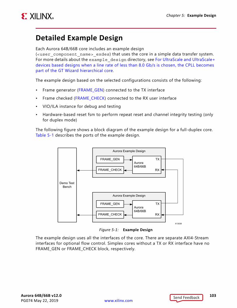
Aurora 64B/66B v12.0 103PG074 May 22, 2019 www.xilinx.com
Chapter 5: Example Design
Detailed Example DesignEach Aurora 64B/66B core includes an example design (<user_component_name>_exdes) that uses the core in a simple data transfer system. For more details about the example_design directory, see For UltraScale and UltraScale+ devices based designs when a line rate of less than 8.0 Gb/s is chosen, the CPLL becomes part of the GT Wizard hierarchical core.
The example design based on the selected configurations consists of the following:
• Frame generator (FRAME_GEN) connected to the TX interface• Frame checked (FRAME_CHECK) connected to the RX user interface• VIO/ILA instance for debug and testing• Hardware-based reset fsm to perform repeat reset and channel integrity testing (only
for duplex mode)
The following figure shows a block diagram of the example design for a full-duplex core. Table 5-1 describes the ports of the example design.
The example design uses all the interfaces of the core. There are separate AXI4-Stream interfaces for optional flow control. Simplex cores without a TX or RX interface have no FRAME_GEN or FRAME_CHECK block, respectively.
X-Ref Target - Figure 5-1
Figure 5-1: Example Design
Demo Test Bench
Aurora Example Design
FRAME_GENAurora64B/66B
FRAME_CHECK
TX
RX
Aurora Example Design
FRAME_GENAurora64B/66B
FRAME_CHECK
TX
RX
X13038
Send Feedback
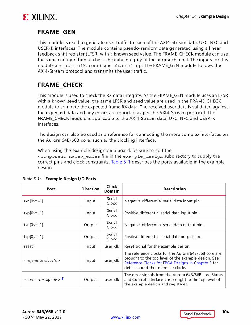
Aurora 64B/66B v12.0 104PG074 May 22, 2019 www.xilinx.com
Chapter 5: Example Design
FRAME_GENThis module is used to generate user traffic to each of the AXI4-Stream data, UFC, NFC and USER-K interfaces. The module contains pseudo-random data generated using a linear feedback shift register (LFSR) with a known seed value. The FRAME_CHECK module can use the same configuration to check the data integrity of the aurora channel. The inputs for this module are user_clk, reset and channel_up. The FRAME_GEN module follows the AXI4-Stream protocol and transmits the user traffic.
FRAME_CHECKThis module is used to check the RX data integrity. As the FRAME_GEN module uses an LFSR with a known seed value, the same LFSR and seed value are used in the FRAME_CHECK module to compute the expected frame RX data. The received user data is validated against the expected data and any errors are reported as per the AXI4-Stream protocol. The FRAME_CHECK module is applicable to the AXI4-Stream data, UFC, NFC and USER-K interfaces.
The design can also be used as a reference for connecting the more complex interfaces on the Aurora 64B/66B core, such as the clocking interface.
When using the example design on a board, be sure to edit the <component name>_exdes file in the example_design subdirectory to supply the correct pins and clock constraints. Table 5-1 describes the ports available in the example design.
Table 5-1: Example Design I/O Ports
Port Direction Clock Domain Description
rxn[0:m–1] Input Serial Clock Negative differential serial data input pin.
rxp[0:m–1] Input Serial Clock Positive differential serial data input pin.
txn[0:m–1] Output Serial Clock Negative differential serial data output pin.
txp[0:m–1] Output Serial Clock Positive differential serial data output pin.
reset Input user_clk Reset signal for the example design.
<reference clock(s)> Input user_clkThe reference clocks for the Aurora 64B/66B core are brought to the top level of the example design. See Reference Clocks for FPGA Designs in Chapter 3 for details about the reference clocks.
<core error signals>(1) Output user_clkThe error signals from the Aurora 64B/66B core Status and Control interface are brought to the top level of the example design and registered.
Send Feedback
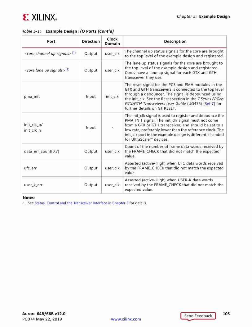
Aurora 64B/66B v12.0 105PG074 May 22, 2019 www.xilinx.com
Chapter 5: Example Design
<core channel up signals>(1) Output user_clk The channel up status signals for the core are brought to the top level of the example design and registered.
<core lane up signals>(1) Output user_clkThe lane up status signals for the core are brought to the top level of the example design and registered. Cores have a lane up signal for each GTX and GTH transceiver they use.
pma_init Input init_clk
The reset signal for the PCS and PMA modules in the GTX and GTH transceivers is connected to the top level through a debouncer. The signal is debounced using the init_clk. See the Reset section in the 7 Series FPGAs GTX/GTH Transceivers User Guide (UG476) [Ref 7] for further details on GT RESET.
init_clk_p/init_clk_n Input -
The init_clk signal is used to register and debounce the PMA_INIT signal. The init_clk signal must not come from a GTX or GTH transceiver, and should be set to a low rate, preferably lower than the reference clock. The init_clk port in the example design is differential-ended for UltraScale™ devices.
data_err_count[0:7] Output user_clkCount of the number of frame data words received by the FRAME_CHECK that did not match the expected value.
ufc_err Output user_clkAsserted (active-High) when UFC data words received by the FRAME_CHECK that did not match the expected value.
user_k_err Output user_clkAsserted (active-High) when USER-K data words received by the FRAME_CHECK that did not match the expected value.
Notes: 1. See Status, Control and the Transceiver Interface in Chapter 2 for details.
Table 5-1: Example Design I/O Ports (Cont’d)
Port Direction Clock Domain Description
Send Feedback
Aurora 64B/66B v12.0 106PG074 May 22, 2019 www.xilinx.com
Chapter 5: Example Design
Using Vivado Lab ToolsThe integrated logic analyzer (ILA) and VIO cores aid in debugging and validating the design in the board and are provided with the Aurora 64B/66B core. The Aurora 64B/66B core connects the relevant signals to the VIO to facilitate easier bring-up or debug of the design. Select the Vivado Lab Tools option from the Core Options tab in the Vivado Integrated Design Environment (IDE) (see Figure 4-1) to include it as a part of the example design.
Cores generated with the Vivado lab tools option enabled have three VIO interfaces and one ILA interface.
• vio1_inst – contains core Lane Up, Channel Up, Data Error count, Soft Error count, Channel Up transition count along with System Reset, GT Reset and Loopback ports
• vio2_inst – contains status of reset quality counters• vio3_inst – contains test pass/fail status for repeat reset test• i_ila – contains core status signals like hard_err, soft_err, channel_up, lane_up,
and data_err and the first 16-bits of tx and rx data.
Implementing the Example DesignThe example design must be generated from the IP core. See Implementing the Example Design earlier in this chapter.
Hardware Reset FSM in the Example DesignThe Aurora 64B/66B core example design for duplex mode incorporates a hardware reset FSM to perform repeated resets and monitoring robustness of the link. This FSM also contains an option to set different time periods between reset assertions. Also continuous channel_up and link_reset transition counters are monitored and the test status is reported through VIO.
The following signals are added in to the default ILA and VIOs for probing the link:
i_ila:
• tx_d_i[0:15]: TX Data from the LocalLink Frame Gen module• rx_d_i[0:15]: RX Data to the LocalLink Frame check module
Send Feedback
Aurora 64B/66B v12.0 107PG074 May 22, 2019 www.xilinx.com
Chapter 5: Example Design
• data_err_count_o: 8-bit Data error count value, it is expected to be 'd0 in normal operations
• lane_up_vio_usrclk: lane_up signal • channel_up_i: channel_up signal• soft_err_i: Soft error monitor• hard_err_i: Hard error monitor
vio1_inst:
• sysreset_from_vio_i: Reset input to example design• gtreset_from_vio_i: pma_init to example design• vio_probe_in2: Quality counters for Link status• rx_cdrovrden_i: Used while enabling loopback mode• loopback_i: Used while enabling loopback mode
vio2_inst:
• reset_quality_cntrs: Used to reset all the quality counters in the example design• reset_test_fsm_from_vio: Used to reset the hardware reset test FSM• reset_test_enable_from_vio: Used to enable/start the repeat reset test from the
vio ports on the hardware.• iteraion_cnt_sel_from_vio: Number of repeat reset iterations to be initiated.
This is a 4-bit encoded value for a fixed number of iterations that can be seen in the example design when Vivado lab tools is enabled.
• lnk_reset_in_initclk: Input probe to monitor the assertion of link_reset • soft_err_in_initclk: Input probe to monitor the soft_err status• chan_up_transcnt_20bit_i [15:8]: Number of channel_up transaction counts;
this can be used to monitor the number of reset iterations that have been completed. Note:
a. chan_up_transcnt_20bit_i is probed only [15:8] bits; hence, this probe takes some time to update the status.
b. To change the number of reset iterations, modify the respective value for iteration_cnt_sel_from_vio and correspondingly select chan_up_transcnt_20bit_i to probe the status.
Send Feedback
Aurora 64B/66B v12.0 108PG074 May 22, 2019 www.xilinx.com
Chapter 5: Example Design
vio3_inst:
• test_passed_r: Test pass status is asserted after the respective iteration count if resets are done successfully.
• test_failed_r: Test fail status is asserted if there is either a lack of channel_up or some data errors have occurred.
• lnkrst_cnt_20bit_vio_i: Probe to monitor the number of times the link_reset is asserted.
• reset_test_fsm_chk_time_sel: 3-bit encoded value probe to select the hardware reset_fsm check time for channel_up assertions after reset is deasserted.
Hardware FSM Operation:
In the example design (<user_component_name>_exdes.v), a hardware initiated repeat reset FSM has been added to test the robustness of the link when subject to repeat reset. The FSM consists of IDLE, ASSERT_RST, DASSERT_RST, WAIT, WAIT1, CHECK, FAIL and DONE states.
1. In IDLE state, test_passed_r indicates reset test passed, test_failed_r indicates reset test fail, and timer_r provides an iteration count of resets. Defaults to 0.
2. When the reset_test_enable_from_vio signal is asserted, the hardware FSM traverses to the ASSERT_RST state where pma_init is asserted for a pre-determined time (28-bit count time).
3. This pma_init assertion ensures that a hot plug sequence is detected by the link partner. The hardware FSM then traverses to the DEASSERT_RST state where the pma_init is deasserted and the timer is loaded with a default value that can be configured using the reset_test_fsm_chk_time_sel vio signal.
4. The FSM then moves to the WAIT state until the selected time has expired. In this state, all checks such as for data errors and soft error occurrences are performed and the channel_up signal is verified to be asserted High and not toggled more than once for this iteration of pma_init.
5. If this condition is not met, the FSM moves to FAIL state and the repeat reset run is stopped. Otherwise, the FSM moves to WAIT1 state where a few data packets are transmitted and received.
6. The FSM then moves to the CHECK state, in which the channel_up transitions are checked again. If there is not more than one transition, the FSM returns to the IDLE state until the requested iterations are completed. This ensures that the link is robust and recovers reliably across multiple repeat resets of the link.
Send Feedback
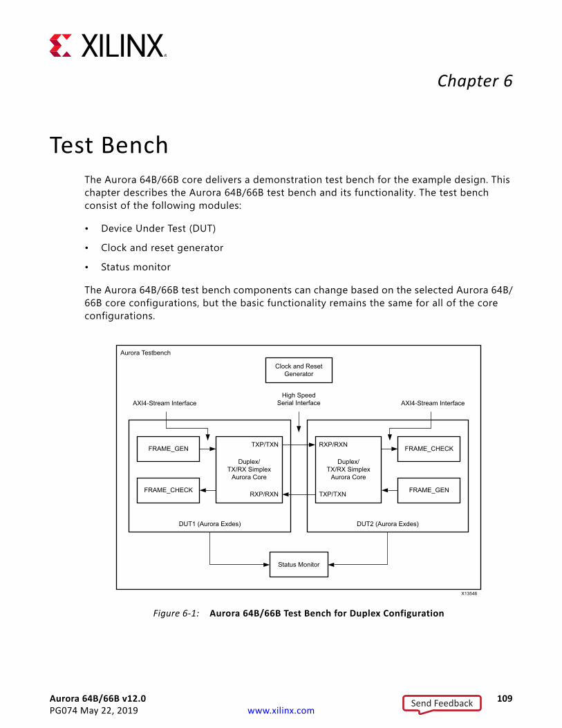
Aurora 64B/66B v12.0 109PG074 May 22, 2019 www.xilinx.com
Chapter 6
Test BenchThe Aurora 64B/66B core delivers a demonstration test bench for the example design. This chapter describes the Aurora 64B/66B test bench and its functionality. The test bench consist of the following modules:
• Device Under Test (DUT) • Clock and reset generator • Status monitor
The Aurora 64B/66B test bench components can change based on the selected Aurora 64B/66B core configurations, but the basic functionality remains the same for all of the core configurations.X-Ref Target - Figure 6-1
Figure 6-1: Aurora 64B/66B Test Bench for Duplex Configuration
Clock and ResetGenerator
DUT1 (Aurora Exdes) DUT2 (Aurora Exdes)
Status Monitor
FRAME_CHECK
Duplex/TX/RX Simplex
Aurora Core
Duplex/TX/RX Simplex
Aurora Core
FRAME_GEN
Aurora Testbench
High SpeedSerial InterfaceAXI4-Stream Interface AXI4-Stream Interface
RXP/RXN
X13546
FRAME_GEN FRAME_CHECK
TXP/TXN
TXP/TXN RXP/RXN
Send Feedback
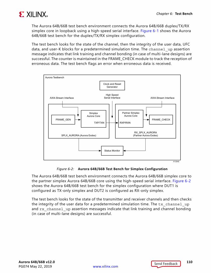
Aurora 64B/66B v12.0 110PG074 May 22, 2019 www.xilinx.com
Chapter 6: Test Bench
The Aurora 64B/66B test bench environment connects the Aurora 64B/66B duplex/TX/RX simplex core in loopback using a high-speed serial interface. Figure 6-1 shows the Aurora 64B/66B test bench for the duplex/TX/RX simplex configuration.
The test bench looks for the state of the channel, then the integrity of the user data, UFC data, and user-K blocks for a predetermined simulation time. The channel_up assertion message indicates that link training and channel bonding (in case of multi-lane designs) are successful. The counter is maintained in the FRAME_CHECK module to track the reception of erroneous data. The test bench flags an error when erroneous data is received.
The Aurora 64B/66B test bench environment connects the Aurora 64B/66B simplex core to the partner simplex Aurora 64B/66B core using the high-speed serial interface. Figure 6-2 shows the Aurora 64B/66B test bench for the simplex configuration where DUT1 is configured as TX-only simplex and DUT2 is configured as RX-only simplex.
The test bench looks for the state of the transmitter and receiver channels and then checks the integrity of the user data for a predetermined simulation time. The tx_channel_up and rx_channel_up assertion messages indicate that link training and channel bonding (in case of multi-lane designs) are successful.
X-Ref Target - Figure 6-2
Figure 6-2: Aurora 64B/66B Test Bench for Simplex Configuration
Clock and ResetGenerator
SPLX_AURORA (Aurora Exdes)RX_SPLX_AURORA
(Partner Aurora Exdes)
Status Monitor
FRAME_GEN
SimplexAurora Core
Partner SimplexAurora Core
FRAME_CHECK
Aurora Testbench
High SpeedSerial InterfaceAXI4-Stream Interface AXI4-Stream Interface
TXP/TXN RXP/RXN
X13545
Send Feedback
Aurora 64B/66B v12.0 111PG074 May 22, 2019 www.xilinx.com
Appendix A
Verification, Compliance, and Interoperability
This appendix provides details about how this IP core was tested for compliance.
Aurora 64B/66B cores are verified for protocol compliance using an array of automated hardware and simulation tests. The core comes with an example design implemented using a linear feedback shift register (LFSR) for understanding and verification of the core features.
Aurora 64B/66B cores are tested in hardware for functionality, performance, and reliability using Xilinx evaluation boards. Aurora 64B/66B verification test suites for all possible modules are continuously being updated to increase test coverage across the range of possible parameters for each individual module.
A series of test scenarios are validated using various Xilinx development boards which are listed in Table A-1. These boards can be used to prototype system designs and the core can be used to communicate with other systems. The testing of Aurora example designs for various configurations are done either by board-to-board testing using standard Bulls eye connectors or SMA connectors. Also external cable loopback tests are performed as part of reset stress testing. The test sequence typically uses Vivado Lab Tools and follows the typical sequence and tests represented in the example design simulation.
To achieve interoperability among different versions of Aurora 64B/66B cores for 7 series FPGA transceivers, a user-level parameter is provided which must be set to achieve proper interoperability between cores as shown in Table A-2. Table A-3 shows the interoperability between 2015.1 (7 series FPGAs) with 2015.1 (UltraScale™ FPGAs) of the Aurora 64B/66B core.
Table A-1: Xilinx Development BoardsTarget Device Evaluation Boards Characterization boards
7 series FPGAs KC705, VC707, VC709, ZC706 KC724, VC7203, VC7215, ZC723UltraScale™ and UltraScale+ devices
KCU105, VCU108, VCU110, KCU114, KCU116
UC1250, UC1283, UC1287, UC1262
Send Feedback
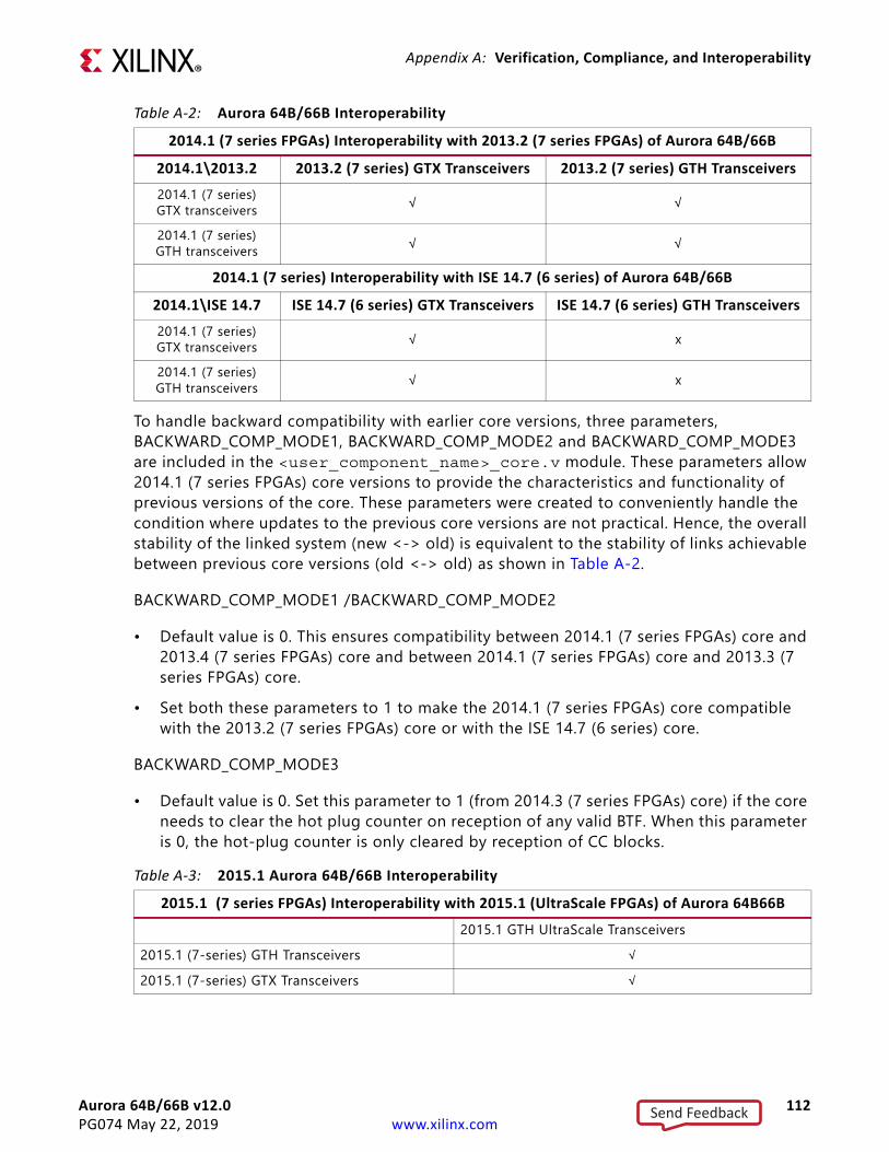
Aurora 64B/66B v12.0 112PG074 May 22, 2019 www.xilinx.com
Appendix A: Verification, Compliance, and Interoperability
To handle backward compatibility with earlier core versions, three parameters, BACKWARD_COMP_MODE1, BACKWARD_COMP_MODE2 and BACKWARD_COMP_MODE3 are included in the <user_component_name>_core.v module. These parameters allow 2014.1 (7 series FPGAs) core versions to provide the characteristics and functionality of previous versions of the core. These parameters were created to conveniently handle the condition where updates to the previous core versions are not practical. Hence, the overall stability of the linked system (new <-> old) is equivalent to the stability of links achievable between previous core versions (old <-> old) as shown in Table A-2.
BACKWARD_COMP_MODE1 /BACKWARD_COMP_MODE2
• Default value is 0. This ensures compatibility between 2014.1 (7 series FPGAs) core and2013.4 (7 series FPGAs) core and between 2014.1 (7 series FPGAs) core and 2013.3 (7series FPGAs) core.
• Set both these parameters to 1 to make the 2014.1 (7 series FPGAs) core compatiblewith the 2013.2 (7 series FPGAs) core or with the ISE 14.7 (6 series) core.
BACKWARD_COMP_MODE3
• Default value is 0. Set this parameter to 1 (from 2014.3 (7 series FPGAs) core) if the coreneeds to clear the hot plug counter on reception of any valid BTF. When this parameteris 0, the hot-plug counter is only cleared by reception of CC blocks.
Table A-2: Aurora 64B/66B Interoperability2014.1 (7 series FPGAs) Interoperability with 2013.2 (7 series FPGAs) of Aurora 64B/66B
2014.1\2013.2 2013.2 (7 series) GTX Transceivers 2013.2 (7 series) GTH Transceivers2014.1 (7 series)GTX transceivers √ √
2014.1 (7 series)GTH transceivers √ √
2014.1 (7 series) Interoperability with ISE 14.7 (6 series) of Aurora 64B/66B2014.1\ISE 14.7 ISE 14.7 (6 series) GTX Transceivers ISE 14.7 (6 series) GTH Transceivers2014.1 (7 series)GTX transceivers √ x
2014.1 (7 series)GTH transceivers √ x
Table A-3: 2015.1 Aurora 64B/66B Interoperability2015.1 (7 series FPGAs) Interoperability with 2015.1 (UltraScale FPGAs) of Aurora 64B66B
2015.1 GTH UltraScale Transceivers2015.1 (7-series) GTH Transceivers √2015.1 (7-series) GTX Transceivers √
Send Feedback
Aurora 64B/66B v12.0 113PG074 May 22, 2019 www.xilinx.com
Appendix B
UpgradingThis appendix contains information about upgrading to a more recent version of the IP core and migrating legacy (LocalLink based) Aurora 64B/66B Cores to the AXI4-Stream Aurora 64B/66B Core.
For customers upgrading in the Vivado® Design Suite, important details (where applicable) about any port changes and other impacts to user logic are included.
Device MigrationIf migrating from a 7 series device with GTX or GTH transceivers to an UltraScale™ device with GTH transceivers, the prefixes of the optional transceiver debug ports for single-lane cores are changed from “gt0”, “gt1” to “gt”, and the suffix “_in” and “_out” are dropped. For multi-lane cores, the prefixes of the optional transceiver debug ports gt(n) are aggregated into a single port. For example: gt0_gtrxreset and gt1_gtrxreset now become gt_gtrxreset [1:0]. This is true for all ports, with the exception of the DRP buses which follow the convention of gt(n)_drpxyz.
IMPORTANT: It is important that designs are updated to use the new transceiver debug port names. For more information about migration to UltraScale devices, see the UltraScale Architecture Migration Methodology Guide (UG1026) [Ref 16].
Send Feedback
Aurora 64B/66B v12.0 114PG074 May 22, 2019 www.xilinx.com
Appendix B: Upgrading
Upgrading in the Vivado Design SuiteThis section provides information about any changes to the user logic or port designations that take place when you upgrade to a more current version of this IP core in the Vivado Design Suite.
In the latest revision of the core, there have been several changes which make the core pin-incompatible with previous versions. These changes were required as part of the general one-off hierarchical changes to enhance the customer experience.
Shared LogicAs part of the hierarchical changes to the core, it is now possible to have the core itself include all of the logic which can be shared between multiple cores, which was previously exposed in the example design for the core.
RECOMMENDED: If upgrading to a later core version with shared logic, there is no simple upgrade path and it is recommended that you consult the Shared Logic sections of this document for more guidance.
Changes from v11.2 to v12.0
Updated the core to v12.0.
Changes from v11.1 to v11.2
Aurora IP can now be generated without GT in UltraScale and UltraScale+ based devices.
Changes from v11.0 to v11.1
Added GTYE4 transceiver support and also added gt_rxusrclk_out transceiver debug output.
Changes from v10.0 to v11.0
Added GTYE3 transceiver support.
Changes from v9.3 to v10.0
Send Feedback
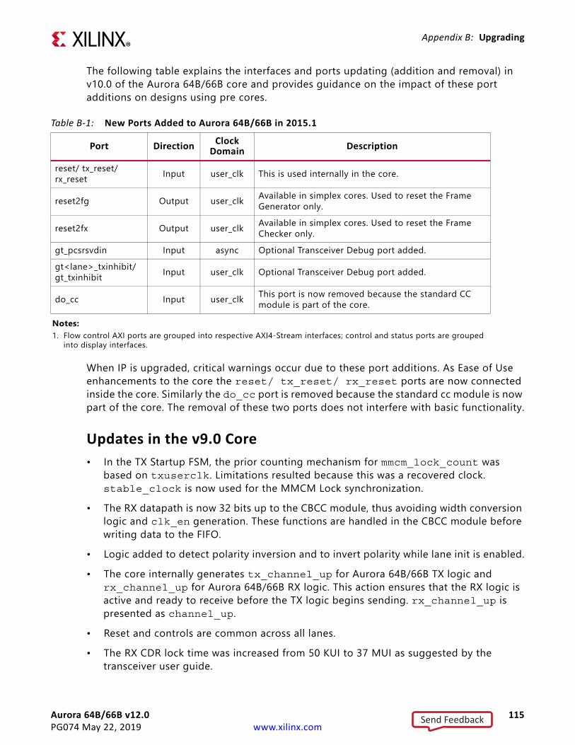
Aurora 64B/66B v12.0 115PG074 May 22, 2019 www.xilinx.com
Appendix B: Upgrading
The following table explains the interfaces and ports updating (addition and removal) in v10.0 of the Aurora 64B/66B core and provides guidance on the impact of these port additions on designs using pre cores.
When IP is upgraded, critical warnings occur due to these port additions. As Ease of Use enhancements to the core the reset/ tx_reset/ rx_reset ports are now connected inside the core. Similarly the do_cc port is removed because the standard cc module is now part of the core. The removal of these two ports does not interfere with basic functionality.
Updates in the v9.0 Core• In the TX Startup FSM, the prior counting mechanism for mmcm_lock_count was
based on txuserclk. Limitations resulted because this was a recovered clock. stable_clock is now used for the MMCM Lock synchronization.
• The RX datapath is now 32 bits up to the CBCC module, thus avoiding width conversion logic and clk_en generation. These functions are handled in the CBCC module before writing data to the FIFO.
• Logic added to detect polarity inversion and to invert polarity while lane init is enabled.• The core internally generates tx_channel_up for Aurora 64B/66B TX logic and
rx_channel_up for Aurora 64B/66B RX logic. This action ensures that the RX logic is active and ready to receive before the TX logic begins sending. rx_channel_up is presented as channel_up.
• Reset and controls are common across all lanes.• The RX CDR lock time was increased from 50 KUI to 37 MUI as suggested by the
transceiver user guide.
Table B-1: New Ports Added to Aurora 64B/66B in 2015.1
Port Direction Clock Domain Description
reset/ tx_reset/ rx_reset Input user_clk This is used internally in the core.
reset2fg Output user_clk Available in simplex cores. Used to reset the Frame Generator only.
reset2fx Output user_clk Available in simplex cores. Used to reset the Frame Checker only.
gt_pcsrsvdin Input async Optional Transceiver Debug port added. gt<lane>_txinhibit/ gt_txinhibit Input user_clk Optional Transceiver Debug port added.
do_cc Input user_clk This port is now removed because the standard CC module is part of the core.
Notes: 1. Flow control AXI ports are grouped into respective AXI4-Stream interfaces; control and status ports are grouped
into display interfaces.
Send Feedback
Aurora 64B/66B v12.0 116PG074 May 22, 2019 www.xilinx.com
Appendix B: Upgrading
• The Block Sync header max count was increased from 64 to 60,000 to improve the robustness of the link.
• Allowed transmission of more idle characters during channel initialization to improve robustness of the link.
• Removed the scrambler reset making it free running to achieve faster CDR lock. The default pattern sent by the scrambler is the scrambled value of NA idle character.
• Updated the GTH transceiver QPLL attributes - See AR 56332.• Added shared logic and optional transceiver control and status debug ports.• Updated clock domain crossing synchronizers to increase Mean Time Between Failures
(MTBF) from meta-stability. Currently using a common synchronizer module and applying false path constraints only for the first stage of the flops.
• Added support for Cadence IES and Synopsys VCS simulators.• Added Vivado lab tools support for debug.• Added quality counters in the example design to increase the test quality.• Added a hardware reset state machine in the example design to perform repeat reset
testing.
Migrating Legacy (LocalLink based) Aurora 64B/66B Cores to the AXI4-Stream Aurora 64B/66B CorePrerequisites • Vivado design tools build containing the Aurora 64B/66B v9.x core supporting the
AXI4-Stream protocol • Familiarity with the Aurora 64B/66B directory structure• Familiarity with running the Aurora 64B/66B example design• Basic knowledge of the AXI4-Stream and LocalLink protocols• Latest product guide (PG074) of the core with the AXI4-Stream updates • Legacy documents: LogiCORE IP Aurora 64B/66B 64B/66B v4.2 Data Sheet (DS528)
[Ref 17], LogiCORE IP Aurora 64B/66B v4.1 Getting Started Guide (UG238) [Ref 18], and LogiCORE IP Aurora 64B/66B v4.2 User Guide (UG237) [Ref 19] for reference.
• Migration guide (this Appendix)
Send Feedback
Aurora 64B/66B v12.0 117PG074 May 22, 2019 www.xilinx.com
Appendix B: Upgrading
Overview of Major ChangesThe major changes to the core is the addition of the AXI4-Stream interface:
• Max line rate support of 16.375G added for UltraScale GTHE3/GTHE4 transceivers.• Extended the Max line rate support of up to 25.7813G for GTYE3/GTYE4 transceivers.• Line rate value restricted to four decimal digits for UltraScale and UltraScale+ devices
with the exception of 25.78125 Gb/s for GTY devices.• GT location selection option for UltraScale device added to the core.• Added support for simplex auto recovery.• Flow control ports grouped into AXI4-Stream interfaces.• Control and Status ports are grouped into display interfaces.• Single-ended clock option added to the core for init_clk and gt_refclk.• Both reset inputs pma_init and reset_pb made asynchronous. The reset,
tx_reset and rx_reset input ports were removed. • CRC resource utilization optimized.• Standard CC module made part of the IP. The do_cc port was removed.• INIT clock frequency value can take up to six decimal digits.
Block DiagramsFigure B-1 shows an example Aurora 64B/66B design using the legacy LocalLink interface. Figure B-2 shows an example Aurora 64B/66B design using the AXI4-Stream interface.
X-Ref Target - Figure B-1
Figure B-1: Legacy Aurora 64B/66B Example Design
LocalLink AURORA DESIGN
LocalLink FRAME GEN
LocalLink FRAME CHECK
LEGACY AURORA EXAMPLE DESIGN
X14621
Send Feedback
Aurora 64B/66B v12.0 118PG074 May 22, 2019 www.xilinx.com
Appendix B: Upgrading
Signal Changes
X-Ref Target - Figure B-2
Figure B-2: AXI4-Stream Aurora 64B/66B Example Design
LocalLink to AX14-Stream
X12662
Existing LocalLink based
DesignAX14-Stream to LocalLink
AX14-Stream Aurora Design
AXI4-Stream Aurora Design Top
Table B-2: Interface ChangesLocalLink Name AXI4-S Name DifferenceTX_D s_axi_tx_tdata Name change only
TX_REM s_axi_tx_tkeep Name change. For functional differences, see Table 2-4
TX_SOF_N Generated InternallyTX_EOF_N s_axi_tx_tlast Name change; PolarityTX_SRC_RDY_N s_axi_tx_tvalid Name change; PolarityTX_DST_RDY_N s_axi_tx_tready Name change; PolarityUFC_TX_REQ_N ufc_tx_req Name change; PolarityUFC_TX_MS ufc_tx_ms No ChangeUFC_TX_D s_axi_ufc_tx_tdata Name change onlyUFC_TX_SRC_RDY_N s_axi_ufc_tx_tvalid Name change; PolarityUFC_TX_DST_RDY_N s_axi_ufc_tx_tready Name change; PolarityNFC_TX_REQ_N s_axi_nfc_tx_tvalid Name change; PolarityNFC_TX_ACK_N s_axi_nfc_tx_tready Name change; PolarityNFC_PAUSE
s_axi_nfc_tx_tdata Name change.For signal mapping, see Table 2-10NFC_XOFF
USER_K_DATAs_axi_user_k_tdata Name change.
For signal mapping, see Table 2-12 USER_K_BLK_NOUSER_K_TX_SRC_RDY_N s_axi_user_k_tx_tvalid Name change; PolarityUSER_K_TX_DST_RDY_N s_axi_user_k_tx_tready Name change; PolarityRX_D m_axi_rx_tdata Name change only
RX_REM m_axi_rx_tkeep Name change.For functional difference, see Table 2-4
RX_SOF_N RemovedRX_EOF_N m_axi_rx_tlast Name change; Polarity
Send Feedback
Aurora 64B/66B v12.0 119PG074 May 22, 2019 www.xilinx.com
Appendix B: Upgrading
Migration StepsGenerate an AXI4-Stream Aurora 64B/66B core from the Vivado design tools.
Simulate the Core
1. Run simulation from the Vivado IDE. Select simulation type to launch.2. QuestaSim launches and compiles the modules.3. The wave_mti.do file loads automatically and populates AXI4-Stream signals.4. Allow the simulation to run. This might take some time.
a. Initially lane up is asserted.b. Channel up is then asserted and the data transfer begins.c. Data transfer from all flow control interfaces now begins.d. Frame checker continuously checks the received data and reports for any data
mismatch.5. A 'TEST PASS' or 'TEST FAIL' status is printed on the QuestaSim console providing the
status of the test.
Implement the Core
1. Click Run Implementation to run synthesis and implementation consecutively.
RX_SRC_RDY_N m_axi_rx_tvalid Name change; PolarityUFC_RX_DATA m_axi_ufc_rx_tdata Name change only
UFC_RX_REM m_axi_ufc_rx_tkeep Name changeFor functional difference, see Table 2-11
UFC_RX_SOF_N RemovedUFC_RX_EOF_N m_axi_ufc_rx_tlast Name change; PolarityUFC_RX_SRC_RDY_N m_axi_ufc_rx_tvalid Name change; PolarityRX_USER_K_DATA
m_axi_rx_user_k_tdata Name changeFor functional difference, see Table 2-12 RX_USER_K_BLK_NO
RX_USER_K_SRC_RDY_N m_axi_rx_user_k_tvalid Name change; Polarity
Table B-2: Interface Changes (Cont’d)
LocalLink Name AXI4-S Name Difference
Send Feedback
Aurora 64B/66B v12.0 120PG074 May 22, 2019 www.xilinx.com
Appendix B: Upgrading
Integrate to an Existing LocalLink-based Aurora 64B/66B Design
1. The Aurora 64B/66B core provides a lightweight 'shim' to interface to any existing LL based interface. The shims are delivered along with the core from the aurora_64b66b_v8_0 version of the core.
2. See Figure B-2 for the emulation of a LL Aurora 64B/66B core from a AXI4-Stream Aurora 64B/66B core.
3. Two shims <user_component_name>_ll_to_axi.v and <user_component_name>_axi_to_ll.v are provided in the src directory of the AXI4-Stream Aurora 64B/66B core.
4. Instantiate both the shims along with <user_component_name>.v in the existing LL based design top.
5. Connect the shim and AXI4-Stream Aurora 64B/66B design as shown in Figure B-2.6. The latest AXI4-Stream Aurora 64B/66B core is now usable in any existing LL design
environment.
Send Feedback
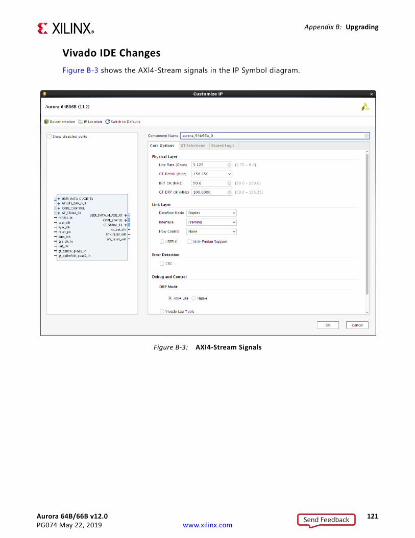
Aurora 64B/66B v12.0 121PG074 May 22, 2019 www.xilinx.com
Appendix B: Upgrading
Vivado IDE ChangesFigure B-3 shows the AXI4-Stream signals in the IP Symbol diagram.
X-Ref Target - Figure B-3
Figure B-3: AXI4-Stream Signals
Send Feedback
Aurora 64B/66B v12.0 122PG074 May 22, 2019 www.xilinx.com
Appendix B: Upgrading
LimitationsThis section outlines the limitations of the Aurora 64B/66B core for AXI4-Stream support.
IMPORTANT: Be aware of the following limitations while interfacing the Aurora 64B/66B core with the AXI4-Stream compliant interface core.
Limitation 1:
The AXI4-Stream specification supports four types of data stream:
• Byte stream • Continuous aligned stream • Continuous unaligned stream • Sparse stream
The Aurora 64B/66B core supports only continuous aligned stream and continuous unaligned stream. The position bytes are valid only at the end of packet.
Limitation 2:
The AXI4-Stream protocol supports transfer with zero data at the end of packet, but the Aurora 64B/66B core expects at least one byte should be valid at the end of packet.
Send Feedback
Aurora 64B/66B v12.0 123PG074 May 22, 2019 www.xilinx.com
Appendix C
DebuggingThis appendix includes details about resources available on the Xilinx Support website and debugging tools.
Finding Help on Xilinx.comTo help in the design and debug process when using the Aurora 64B/66B core, the Xilinx Support web page contains key resources such as product documentation, release notes, answer records, information about known issues, and links for obtaining further product support. Also see the Aurora home page.
DocumentationThis product guide is the main document associated with the Aurora 64B/66B core. This guide, along with documentation related to all products that aid in the design process, can be found on the Xilinx Support web page or by using the Xilinx Documentation Navigator.
Download the Xilinx Documentation Navigator from the Downloads page. For more information about this tool and the features available, open the online help after installation.
To see the available documentation by family, visit the Xilinx Support web page.
To see the available documentation by solution:
1. Visit the Xilinx Support web page.2. Select the Documentation tab located at the top of the web page.
This is the Documentation Center where Xilinx documentation is sorted by Devices, Boards, IP, Design Tools, Doc Type, and Topic.
Send Feedback
Aurora 64B/66B v12.0 124PG074 May 22, 2019 www.xilinx.com
Appendix C: Debugging
Solution CentersSee the Aurora Solutions Center for support specific to the Aurora 64B/66B core. Also, see GT_Debug_Flowchart for transceiver debugging mentioned in the Answer Record, AR: 57237.
Answer RecordsAnswer Records include information about commonly encountered problems, helpful information on how to resolve these problems, and any known issues with a Xilinx product. Answer Records are created and maintained daily ensuring that users have access to the most accurate information available.
Answer Records for this core can be located by using the Search Support box on the main Xilinx support web page. To maximize your search results, use proper keywords such as
• Product name• Tool message(s)• Summary of the issue encountered
A filter search is available after results are returned to further target the results.
To use the Answers Database Search:
3. Enter keywords in the provided search field and select Search.
° Examples of searchable keywords are product names, error messages, or a generic summary of the issue encountered.
° To see all answer records directly related to the Aurora 64B/66B core, search for the phrase "Aurora 64B66B"
Master Answer Record for the Aurora 64B/66B Core
AR: 54368
Xilinx provides premier technical support for customers encountering issues that require additional assistance.
Technical SupportXilinx provides technical support at the Xilinx Support web page for this LogiCORE™ IP product when used as described in the product documentation. Xilinx cannot guarantee timing, functionality, or support if you do any of the following:
• Implement the solution in devices that are not defined in the documentation.• Customize the solution beyond that allowed in the product documentation.
Send Feedback
Aurora 64B/66B v12.0 125PG074 May 22, 2019 www.xilinx.com
Appendix C: Debugging
• Change any section of the design labeled DO NOT MODIFY.
To contact Xilinx Technical Support, The XCI file created during Aurora 64B/66B core generation
Vivado Design Suite Debug FeatureThe Vivado Design Suite debug feature inserts logic analyzer and virtual I/O cores directly into your design. The debug feature also allows you to set trigger conditions to capture application and integrated block port signals in hardware. Captured signals can then be analyzed. This feature in the Vivado IDE is used for logic debugging and validation of a design running in Xilinx.
Note: The init_clk_in clock input is provided as a stable and free running clock to drive the Debug cores and the stability of this clock source is key to ensure the proper debug. You must ensure that this clock is stable before the pma_init input of the IP is de-asserted and that the clock is always stable.
Simulation DebugLanes and Channel Do Not Come Up in Simulation• The quickest way to debug this issue is to view the signals from one of the GT
transceiver instances that is not working.• Ensure that the reference clock and user clocks are all toggling.
Note: Only one of the reference clocks should be toggling, The rest are tied Low.• Check to see that recclk and txoutclk are toggling. If they are not toggling, it
might be necessary to wait longer for the PMA to finish locking. Wait for lane up and channel up. It might be necessary to wait longer for simplex/7 series FPGA designs.
• Ensure that txn and txp are toggling. If they are not, make sure to wait long enough (see the previous bulleted item) and make sure that another signal is not driving the txn/txp signal.
• Check in the <user_component_name>_support module whether the pll/mmcm_not_locked signal and the reset signals are present in the design. If these are being held active, the Aurora 64B/66B module cannot initialize.
• Ensure that the power_down signal is not being asserted.• Ensure that the txn and txp signals from each GTX or GTH transceiver are connected
to the appropriate rxn and rxp signals from the corresponding GTX or GTH transceiver on the other side of the channel
Send Feedback
Aurora 64B/66B v12.0 126PG074 May 22, 2019 www.xilinx.com
Appendix C: Debugging
• Instantiate the "glbl" module and use it to drive the power_up reset at the beginning of the simulation to simulate the reset that occurs after configuration. Hold this reset for a few cycles. The following code can be used an example://Simulate the global reset that occurs after configuration at the beginning//of the simulation.assign glbl.GSR = gsr_r;assign glbl.GTS = gts_r;
initialbegin
gts_r = 1'b0;gsr_r = 1'b1;#(16*CLOCKPERIOD_1);gsr_r = 1'b0;
end
• If you assert rx_reset while using Timer mode and simplex configuration, you should also assert tx_reset. This is to ensure that the core transmits the required initialization patterns for the rx_lane_up and rx_channel_up to come back. However, because of Simplex auto recovery logic, the RX could attain the rx_channel_up state if you wait for sufficient time. In this scenario, the TX transmits periodic patterns that aid in recovering links automatically.
• If you are using a multilane channel, make sure all of the transceivers on each side of the channel are connected in the correct order.
Channel Comes Up in Simulation But s_axi_tx_tready is Never Asserted (Never Goes High)• If the module includes flow control but it is not being used, make sure the request
signals are not currently driven High. s_axi_nfc_tx_tvalid and ufc_tx_req are active-High: if they are High, s_axi_tx_tready stays Low because the channel is allocated for flow control.
• If the module includes USER-K blocks but they are not being used, make sure the s_axi_user_k_tx_tvalid is not driven High. If it is High, s_axi_tx_tready stays Low as channel is allocated for USER-K Blocks.
• If NFC is enabled, make sure the design on the other side of the channel did not send an NFC XOFF message. This cuts off the channel for normal data until the other side sends an NFC XON message to turn the flow on again.
Bytes and Words Are Being Lost As They Travel Through the Aurora 64B/66B Channel• If using the AXI4-Stream interface, make sure to write data correctly. The most common
mistake is to assume words are written without looking at s_axi_tx_tready. Also remember that the s_axi_tx_tkeep signal must be used to indicate which bytes are valid when s_axi_tx_tlast is asserted.
Send Feedback
Aurora 64B/66B v12.0 127PG074 May 22, 2019 www.xilinx.com
Appendix C: Debugging
• Ensure to read correctly from the RX interface. Data and framing signals are only valid when m_axi_rx_tvalid is asserted.
Problems While Compiling the DesignEnsure to include all the files from the src directory when compiling. Check if the simulator and libraries are set up properly. Check if the simulator language is set to mixed.
Next StepOpen a support case to have the appropriate Xilinx expert assist with the issue.
To create a technical support case, see the Xilinx Service Portal web page.
Items to include when opening a case:
• Detailed description of the issue• Results of the steps listed previously• Attach a value change dump (VCD) or wave log format (WLF) dump of the observation.• Attach the XCI/XCO file from the IP.• If any modifications are updated to the IP generated out of Vivado and reasons for
doing the changes.• The.ila dump of the Hardware captures optionally, if available.
Hardware DebugMost fields in the Vivado® Integrated Design Environment (IDE) have tool tips serving as guidelines to properly configure and generate the core.
Observe and follow all RECOMMENDED and IMPORTANT notes in product guides.
As the transceiver is the critical building block in the Aurora 64B/66B core, debugging and ensuring proper operation of the transceiver is extremely important. Figure C-1 shows the steps involved for debugging transceiver-related issues.
IMPORTANT: Ensure that the serial transceiver attributes are updated. See Appendix D, Generating a GT Wrapper File from the Transceiver Wizard for information regarding updating the serial transceiver attribute settings.
Send Feedback
Aurora 64B/66B v12.0 128PG074 May 22, 2019 www.xilinx.com
Appendix C: Debugging
This section provides a debug flow diagram for resolving some of the most common issues. See GT_Debug_Flowchart for transceiver debugging mentioned in the following Answer Record:
AR: 57237
The Transceiver Debug ports mentioned in Table 2-14 are operational when you enable the Additional Transceiver Control and Status Ports option in Aurora 64B/66B interface. Refer to Aurora 64B/66B IP Example design for recommended connections for additional transceiver control and status ports in the following guides:
• 7 Series FPGAs GTX/GTH Transceivers User Guide (UG476) [Ref 7]
• UltraScale Architecture GTH Transceivers User Guide (UG576) [Ref 5]
• UltraScale Architecture GTY Transceivers User Guide (UG578) [Ref 6]
Send Feedback
Aurora 64B/66B v12.0 129PG074 May 22, 2019 www.xilinx.com
Appendix C: Debugging
X-Ref Target - Figure C-1
Figure C-1: Transceiver Debug Flow Chart
START
Transceiver Attribute Check (Step 1)
GT REFCLK and GT PLL LOCK Check (Step 2)
GT TX/RX RESETDONE Check (Step 3)
USER_CLK Generation Check (Step 4)
MMCM Lock Check(Step 5)
Block Sync Check(Step 6)
LANE_UP Assertion Check (Step 7)
Single Lane? NoYes
Channel Bonding Assertion Check (Step 8)
CHANNEL_UP Assertion Check (Step 8)
CHANNEL_UP Assertion Check (Step 9)
Periodic Channel Failures Check (Step 10)
Periodic Channel Failures Check (Step 9)
Data Transfer Check(Step 11)
LOOPBACK Testing Check(Step 12)
END
Send Feedback
Aurora 64B/66B v12.0 130PG074 May 22, 2019 www.xilinx.com
Appendix C: Debugging
1. Transceiver Attribute Check
Transceiver attributes must match with the silicon version of the device being used on the board. Apply all the applicable workarounds and Answer Records given for the relevant silicon version.
2. GT REFCLK and GT PLL LOCK Check
A low-jitter differential clock must be provided as the transceiver reference clock. Ensure that REFCLK location constraints are correct with respect to the board schematics. REFCLK should be active and should meet the phase noise requirements of the transceiver. Ensure that the transceiver locks into the incoming GT REFCLK and asserts the gt_pll_lock signal. This signal is available in the Aurora 64B/66B example design. If the gt_pll_lock signal is toggling periodically, check if FSM_RESETDONE is also toggling. Ensure that the GT PLL attributes are set correctly and that the transceiver generates txoutclk with the expected frequency for the given line rate and datapath width options. Note that the Aurora 64B/66B core uses channel PLL/Quad PLL (CPLL/QPLL) in the generated core for GTX or GTH transceivers.
3. GT TX/RX RESETDONE Check
The Aurora 64B/66B core uses the sequential reset mode; all of the transceiver components are reset sequentially, one after another. txresetdone and rxresetdone signals should be asserted at the end of the transceiver initialization. In general, rxresetdone assertion takes longer compared to the txresetdone assertion. Ensure the gt_reset signal pulse width duration matches with the respective transceiver guideline. Probe the signals and FSM states from the RX/TX STARTUP FSM module.
4. USER_CLK Generation Check
The transceiver generates txoutclk based on the line rate parameter. The user_clk signal is generated from txoutclk and the Aurora 64B/66B core uses it as an FPGA logic clock. Check that user_clk is generated properly with the expected frequency from txoutclk. If the user_clk frequency is not in the expected range, check the frequency of the transceiver reference clock and PLL attributes.
5. MMCM Lock Check
Aurora 64B/66B cores expect all clocks to be stable. If clocks are generated using an MMCM, ensure the reset inputs are held High until the generated clock is stable. It is recommended to stop the output clock from the MMCM until it is locked. This can be accomplished by using a BUFGCE with the output clock where clock enable (CE) is driven by the MMCM lock output. If the MMCM_LOCK signal is toggling periodically, check if the TX_STARTUP_FSM is restarting and probe the signals and states of the FSM.
Send Feedback
Aurora 64B/66B v12.0 131PG074 May 22, 2019 www.xilinx.com
Appendix C: Debugging
6. BLOCK SYNC Check
See the block sync algorithm described in the Aurora 64B/66B Protocol Specification (SP011) [Ref 9] for block sync done.
7. LANE_UP Assertion Check
Assertion of the lane_up signal indicates the communication between the transceiver and its channel partner is established and link training is successful. Enable loopback mode and check for lane_up assertions. Bring the LANE_INIT_SM module FSM state signals to debug if lane_up is not asserted. See the Lane Initialization Procedure in the Aurora 64B/66B Protocol Specification (SP011) [Ref 9] for lane_up assertion details.
Single Lane:
8. CHANNEL_UP Assertion Check
The criteria for channel_up signal assertion are the verification sequence (defined in the Aurora 64B/66B protocol) being transferred between channel partners, and the successful reception of four verification sequences. Enable loopback mode and check for lane_up assertions. Bring the CHANNEL_INIT_SM module FSM state signals to debug if channel_up is not asserted. For a simplex link, the simplex TX partner might have already achieved channel_up status. See the Channel Verification Procedure in the Aurora 64B/66B Protocol Specification (SP011) [Ref 9] for channel_up assertion details.
9. Periodic Channel Failures Check
If the Aurora 64B/66B core asserts and deasserts the channel_up signal, enable internal loopback and check for a stable channel up condition. Probe RXBUFSTATUS of the transceiver.
Multiple Lane:
8. Channel Bonding Assertion Check
Channel bonding is necessary for a multi-lane Aurora 64B/66B design. Channel bonding is performed by the transceiver and the required logic is present in the transceiver_wrapper module. Ensure that channel bonding level, master and slave connections are correct. See the channel bonding procedure in the Aurora 64B/66B Protocol Specification (SP011) [Ref 9] for channel_up assertion details.
9. CHANNEL_UP Assertion Check
(See Single Lane, step 8)
Send Feedback
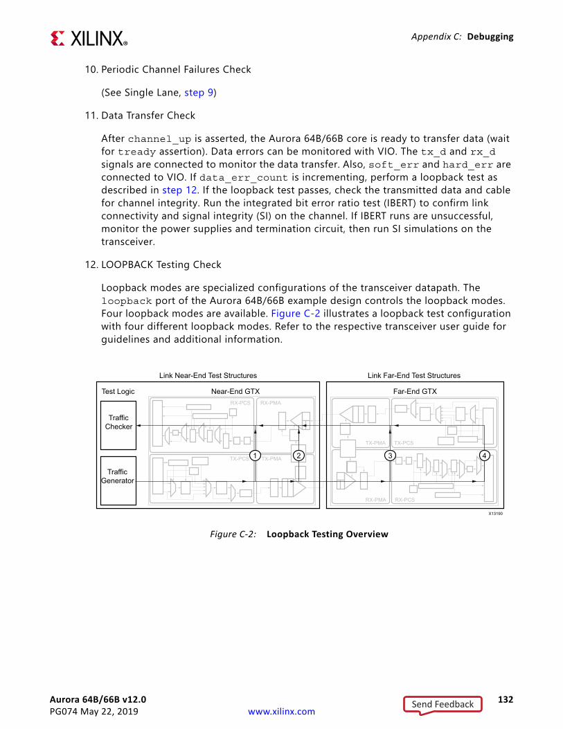
Aurora 64B/66B v12.0 132PG074 May 22, 2019 www.xilinx.com
Appendix C: Debugging
10. Periodic Channel Failures Check
(See Single Lane, step 9)
11. Data Transfer Check
After channel_up is asserted, the Aurora 64B/66B core is ready to transfer data (wait for tready assertion). Data errors can be monitored with VIO. The tx_d and rx_d signals are connected to monitor the data transfer. Also, soft_err and hard_err are connected to VIO. If data_err_count is incrementing, perform a loopback test as described in step 12. If the loopback test passes, check the transmitted data and cable for channel integrity. Run the integrated bit error ratio test (IBERT) to confirm link connectivity and signal integrity (SI) on the channel. If IBERT runs are unsuccessful, monitor the power supplies and termination circuit, then run SI simulations on the transceiver.
12. LOOPBACK Testing Check
Loopback modes are specialized configurations of the transceiver datapath. The loopback port of the Aurora 64B/66B example design controls the loopback modes. Four loopback modes are available. Figure C-2 illustrates a loopback test configuration with four different loopback modes. Refer to the respective transceiver user guide for guidelines and additional information.
X-Ref Target - Figure C-2
Figure C-2: Loopback Testing Overview
Test Logic Near-End GTX
1 2 3 4
Far-End GTX
Link Near-End Test Structures Link Far-End Test Structures
TrafficChecker
TrafficGenerator
RX-PCS
RX-PCS
TX-PCS
TX-PCS
TX-PMA
TX-PMA
RX-PMA
RX-PMA
X13190
Send Feedback
Aurora 64B/66B v12.0 133PG074 May 22, 2019 www.xilinx.com
Appendix C: Debugging
Design Bring-Up on the KC705 Evaluation BoardFor detailed procedures to set up and operate the Aurora 64B/66B core on the KC705 evaluation board, see Designing a System Using the Aurora 64B66B Core (Duplex) on the KC705 Evaluation Kit Application Note (XAPP1192) [Ref 15].
Interface DebugIf data is not being transmitted or received for the AXI4-Stream Interfaces, check the following conditions:
• If transmit s_axi_tx_tready is stuck Low following the s_axi_tx_tvalid input being asserted, the core cannot send data.
• If the receive s_axi_tx_tvalid is stuck Low, the core is not receiving data.• Check that the user_clk inputs are connected and toggling.• Check that the AXI4-Stream waveforms are being followed. See Figure 2-8.• Check core configuration.
Send Feedback
Aurora 64B/66B v12.0 134PG074 May 22, 2019 www.xilinx.com
Appendix D
Generating a GT Wrapper File from the Transceiver Wizard
The transceiver attributes play a vital role in the functionality of the Xilinx® LogiCORE™ IP Aurora 64B/66B core. Use the latest transceiver wizard to generate the transceiver wrapper file.
RECOMMENDED: Xilinx strongly recommends updating the transceiver wrapper file in the Vivado® Design Suite tool releases when the transceiver wizard has been updated but the Aurora 64B/66B core has not.
Use these steps to generate the transceiver wrapper file using the 7 series FPGAs Transceivers Wizard:
1. Using the Vivado IP Catalog, run the latest version of the 7 series FPGAs Transceivers Wizard. Ensure the Component Name of the transceiver wizard matches the Component Name of the Aurora 64B/66B core.
2. Select the protocol template: Aurora 64B/66B. 3. Set the Line Rate for both the TX and RX transceivers based on the application
requirement.4. Select the Reference Clock from the drop-down menu for both the TX and RX
transceivers based on the application requirement.5. Select transceiver(s) and the clock source(s) based on the application requirement.6. On Page 3, select External Data Width of the RX transceiver to be 32 Bits and Internal
Data Width to be 32 bits. Ensure that the TX transceiver is configured with 64-bit external data width and 32-bit internal data width.
7. Keep all other settings as default.8. Generate the core.9. Replace the <user_component_name>_gtx.v file in the example_design/gt/
directory available in the Aurora 64B/66B core with the generated <user_component_name>_gt.v file generated from the 7 series FPGAs Transceivers Wizard.
The transceiver settings for the Aurora 64B/66B core are now up to date.
Note: The UltraScale™ architecture Aurora 64B/66B core uses the hierarchical core calling method to call the UltraScale device GTWizard IP core. In this way, all the transceiver attributes, parameters, and required workarounds are up to date. Manual editing of the UltraScale device transceiver files are not required in most cases.
Send Feedback
Aurora 64B/66B v12.0 135PG074 May 22, 2019 www.xilinx.com
Appendix E
Additional Resources and Legal Notices
Xilinx ResourcesFor support resources such as Answers, Documentation, Downloads, and Forums, see Xilinx Support.
Documentation Navigator and Design HubsXilinx® Documentation Navigator provides access to Xilinx documents, videos, and support resources, which you can filter and search to find information. To open the Xilinx Documentation Navigator (DocNav):
• From the Vivado® IDE, select Help > Documentation and Tutorials.• On Windows, select Start > All Programs > Xilinx Design Tools > DocNav.• At the Linux command prompt, enter docnav.
Xilinx Design Hubs provide links to documentation organized by design tasks and other topics, which you can use to learn key concepts and address frequently asked questions. To access the Design Hubs:
• In the Xilinx Documentation Navigator, click the Design Hubs View tab.• On the Xilinx website, see the Design Hubs page.Note: For more information on Documentation Navigator, see the Documentation Navigator page on the Xilinx website.
ReferencesThese documents provide supplemental material useful with this product guide:
1. Virtex UltraScale FPGAs Data Sheet: DC and AC Switching Characteristics (DS893)2. Kintex UltraScale FPGAs Data Sheet: DC and AC Switching Characteristics (DS892)3. 7 Series FPGAs Overview (DS180)
Send Feedback
Aurora 64B/66B v12.0 136PG074 May 22, 2019 www.xilinx.com
Appendix E: Additional Resources and Legal Notices
4. UltraScale Architecture and Product Overview (DS890)5. UltraScale Architecture GTH Transceivers User Guide (UG576)6. UltraScale Architecture GTY Transceivers User Guide (UG578)7. 7 Series FPGAs GTX/GTH Transceivers User Guide (UG476)8. ARM AMBA 4 AXI4-Stream Protocol v1.0 Specification (ARM IHI 0051A)9. Aurora 64B/66B Protocol Specification (SP011)10. Vivado AXI Reference Guide (UG1037)11. Vivado Design Suite User Guide: Designing IP Subsystems using IP Integrator (UG994)12. Vivado Design Suite User Guide: Designing with IP (UG896)13. Vivado Design Suite User Guide: Getting Started (UG910)14. Vivado Design Suite User Guide - Logic Simulation (UG900)15. Designing a System Using the Aurora 64B66B Core (Duplex) on the KC705 Evaluation Kit
Application Note (XAPP1192)16. UltraScale Architecture Migration Methodology Guide (UG1026)17. LogiCORE IP Aurora 64B/66B v4.2 Data Sheet (DS528)18. LogiCORE IP Aurora 64B/66B v4.1 Getting Started Guide (UG238)19. LogiCORE IP Aurora 64B/66B v4.2 User Guide (UG237)20. ISE to Vivado Design Suite Migration Guide (UG911)21. Vivado Design Suite User Guide: Programming and Debugging (UG908)22. Virtex-7 FPGAs Data Sheet: DC and Switching Characteristics (DS183)23. Kintex-7 FPGAs Data Sheet: DC and Switching Characteristics (DS182)24. Synthesis and Simulation Design Guide (UG626)25. Packaging Custom AXI IP for Vivado IP Integrator Application Note (XAPP1168)26. LogiCORE IP Aurora 64B/66B v7.3 Product Guide (PG074)27. UltraScale FPGAs Transceivers Wizard LogiCORE IP Product Guide (PG182)28. Kintex UltraScale+ FPGAs Data Sheet: DC and AC Switching Characteristics (DS922)29. Virtex UltraScale+ FPGAs Data Sheet: DC and AC Switching Characteristics (DS923)
Send Feedback
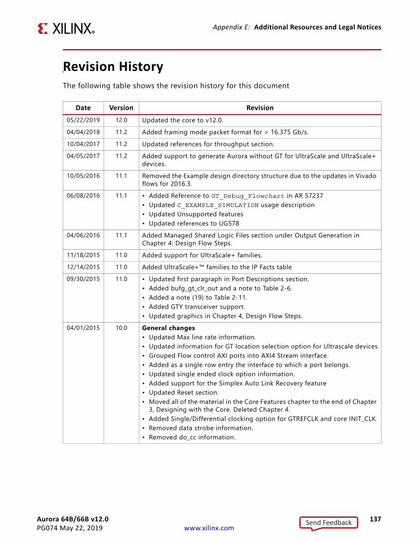
Aurora 64B/66B v12.0 137PG074 May 22, 2019 www.xilinx.com
Appendix E: Additional Resources and Legal Notices
Revision HistoryThe following table shows the revision history for this document
Date Version Revision05/22/2019 12.0 Updated the core to v12.0.04/04/2018 11.2 Added framing mode packet format for > 16.375 Gb/s.10/04/2017 11.2 Updated references for throughput section.04/05/2017 11.2 Added support to generate Aurora without GT for UltraScale and UltraScale+
devices.10/05/2016 11.1 Removed the Example design directory structure due to the updates in Vivado
flows for 2016.3.06/08/2016 11.1 • Added Reference to GT_Debug_Flowchart in AR 57237
• Updated C_EXAMPLE_SIMULATION usage description• Updated Unsupported features• Updated references to UG578
04/06/2016 11.1 Added Managed Shared Logic Files section under Output Generation in Chapter 4: Design Flow Steps.
11/18/2015 11.0 Added support for UltraScale+ families.12/14/2015 11.0 Added UltraScale+™ families to the IP Facts table09/30/2015 11.0 • Updated first paragraph in Port Descriptions section.
• Added bufg_gt_clr_out and a note to Table 2-6.• Added a note (19) to Table 2-11.• Added GTY transceiver support.• Updated graphics in Chapter 4, Design Flow Steps.
04/01/2015 10.0 General changes• Updated Max line rate information.• Updated information for GT location selection option for Ultrascale devices• Grouped Flow control AXI ports into AXI4 Stream interface.• Added as a single row entry the interface to which a port belongs.• Updated single ended clock option information.• Added support for the Simplex Auto Link Recovery feature• Updated Reset section.• Moved all of the material in the Core Features chapter to the end of Chapter
3, Designing with the Core. Deleted Chapter 4.• Added Single/Differential clocking option for GTREFCLK and core INIT_CLK• Removed data strobe information.• Removed do_cc information.
Send Feedback
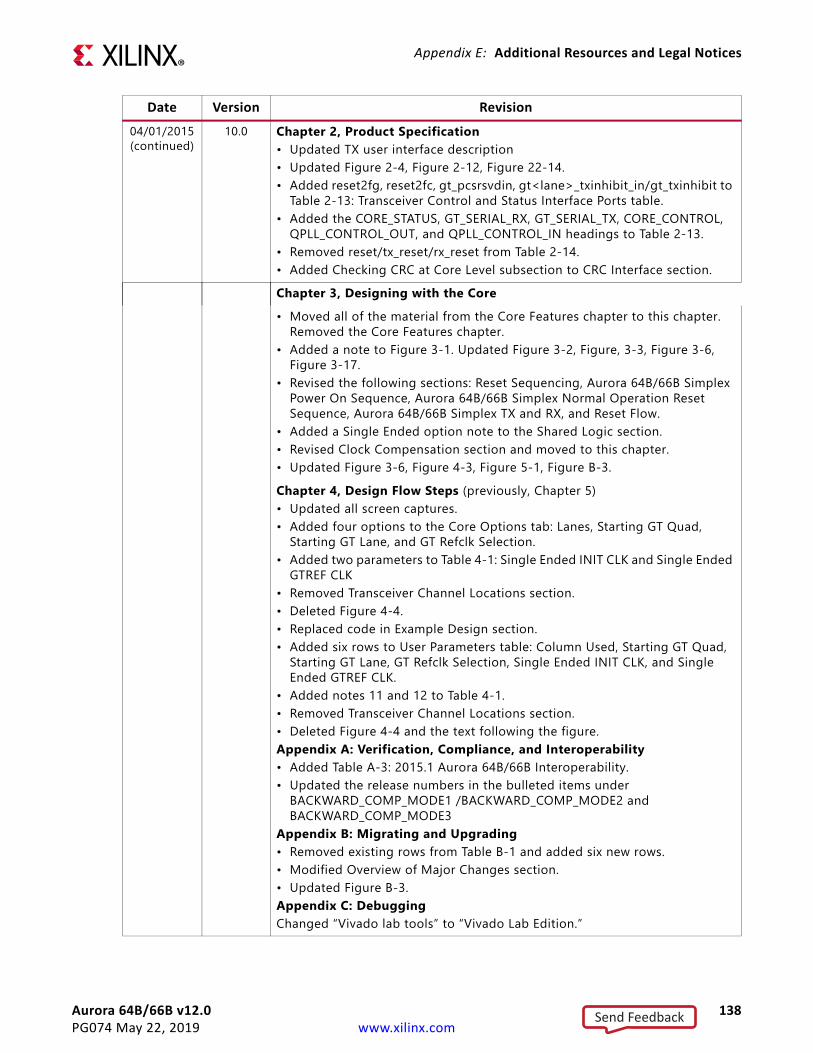
Aurora 64B/66B v12.0 138PG074 May 22, 2019 www.xilinx.com
Appendix E: Additional Resources and Legal Notices
04/01/2015(continued)
10.0 Chapter 2, Product Specification• Updated TX user interface description• Updated Figure 2-4, Figure 2-12, Figure 22-14.• Added reset2fg, reset2fc, gt_pcsrsvdin, gt<lane>_txinhibit_in/gt_txinhibit to
Table 2-13: Transceiver Control and Status Interface Ports table.• Added the CORE_STATUS, GT_SERIAL_RX, GT_SERIAL_TX, CORE_CONTROL,
QPLL_CONTROL_OUT, and QPLL_CONTROL_IN headings to Table 2-13.• Removed reset/tx_reset/rx_reset from Table 2-14.• Added Checking CRC at Core Level subsection to CRC Interface section.Chapter 3, Designing with the Core• Moved all of the material from the Core Features chapter to this chapter.
Removed the Core Features chapter.• Added a note to Figure 3-1. Updated Figure 3-2, Figure, 3-3, Figure 3-6,
Figure 3-17.• Revised the following sections: Reset Sequencing, Aurora 64B/66B Simplex
Power On Sequence, Aurora 64B/66B Simplex Normal Operation Reset Sequence, Aurora 64B/66B Simplex TX and RX, and Reset Flow.
• Added a Single Ended option note to the Shared Logic section.• Revised Clock Compensation section and moved to this chapter.• Updated Figure 3-6, Figure 4-3, Figure 5-1, Figure B-3.Chapter 4, Design Flow Steps (previously, Chapter 5)• Updated all screen captures.• Added four options to the Core Options tab: Lanes, Starting GT Quad,
Starting GT Lane, and GT Refclk Selection.• Added two parameters to Table 4-1: Single Ended INIT CLK and Single Ended
GTREF CLK• Removed Transceiver Channel Locations section.• Deleted Figure 4-4.• Replaced code in Example Design section.• Added six rows to User Parameters table: Column Used, Starting GT Quad,
Starting GT Lane, GT Refclk Selection, Single Ended INIT CLK, and Single Ended GTREF CLK.
• Added notes 11 and 12 to Table 4-1.• Removed Transceiver Channel Locations section.• Deleted Figure 4-4 and the text following the figure.Appendix A: Verification, Compliance, and Interoperability• Added Table A-3: 2015.1 Aurora 64B/66B Interoperability.• Updated the release numbers in the bulleted items under
BACKWARD_COMP_MODE1 /BACKWARD_COMP_MODE2 and BACKWARD_COMP_MODE3
Appendix B: Migrating and Upgrading• Removed existing rows from Table B-1 and added six new rows.• Modified Overview of Major Changes section.• Updated Figure B-3.Appendix C: DebuggingChanged “Vivado lab tools” to “Vivado Lab Edition.”
Date Version Revision
Send Feedback
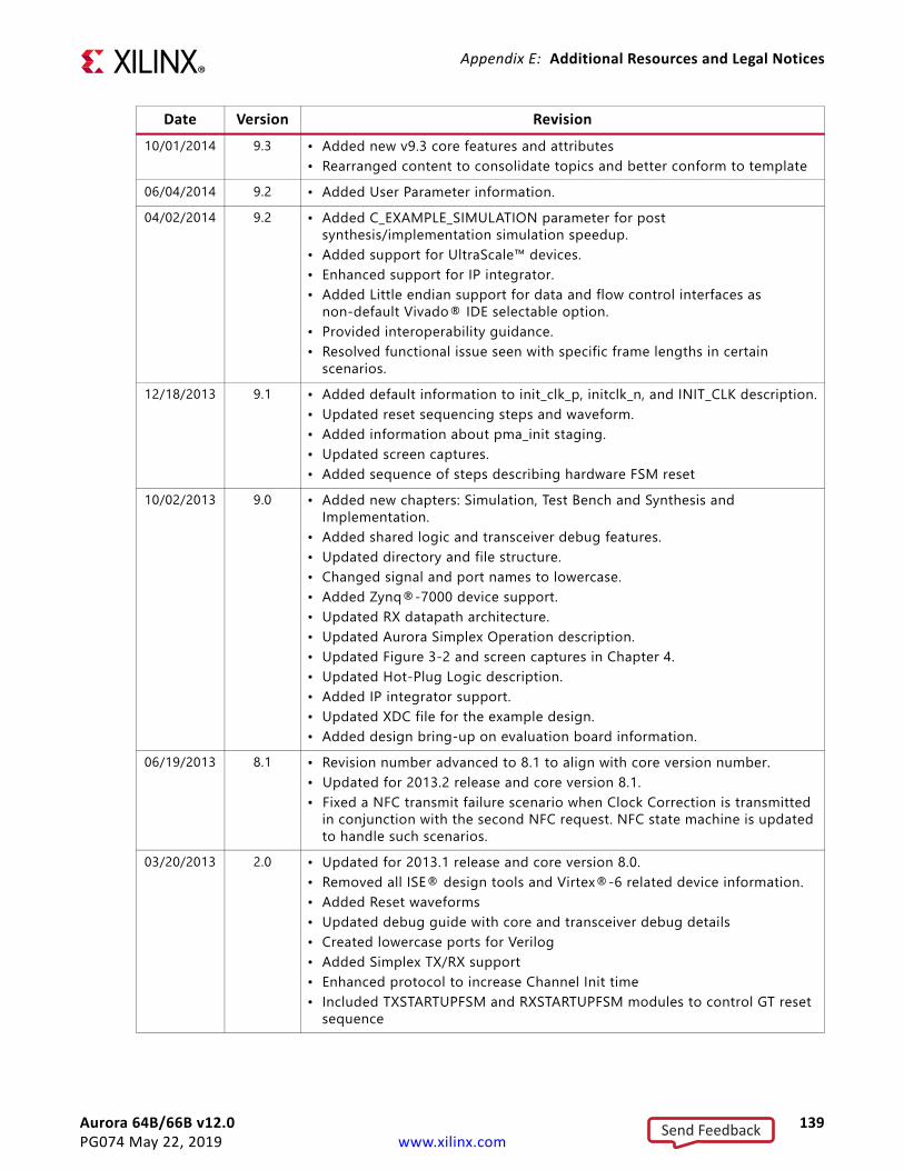
Aurora 64B/66B v12.0 139PG074 May 22, 2019 www.xilinx.com
Appendix E: Additional Resources and Legal Notices
10/01/2014 9.3 • Added new v9.3 core features and attributes• Rearranged content to consolidate topics and better conform to template
06/04/2014 9.2 • Added User Parameter information.04/02/2014 9.2 • Added C_EXAMPLE_SIMULATION parameter for post
synthesis/implementation simulation speedup.• Added support for UltraScale™ devices.• Enhanced support for IP integrator.• Added Little endian support for data and flow control interfaces as
non-default Vivado® IDE selectable option.• Provided interoperability guidance.• Resolved functional issue seen with specific frame lengths in certain
scenarios.12/18/2013 9.1 • Added default information to init_clk_p, initclk_n, and INIT_CLK description.
• Updated reset sequencing steps and waveform.• Added information about pma_init staging.• Updated screen captures.• Added sequence of steps describing hardware FSM reset
10/02/2013 9.0 • Added new chapters: Simulation, Test Bench and Synthesis and Implementation.
• Added shared logic and transceiver debug features. • Updated directory and file structure.• Changed signal and port names to lowercase.• Added Zynq®-7000 device support.• Updated RX datapath architecture.• Updated Aurora Simplex Operation description.• Updated Figure 3-2 and screen captures in Chapter 4.• Updated Hot-Plug Logic description.• Added IP integrator support.• Updated XDC file for the example design.• Added design bring-up on evaluation board information.
06/19/2013 8.1 • Revision number advanced to 8.1 to align with core version number.• Updated for 2013.2 release and core version 8.1.• Fixed a NFC transmit failure scenario when Clock Correction is transmitted
in conjunction with the second NFC request. NFC state machine is updated to handle such scenarios.
03/20/2013 2.0 • Updated for 2013.1 release and core version 8.0.• Removed all ISE® design tools and Virtex®-6 related device information.• Added Reset waveforms• Updated debug guide with core and transceiver debug details• Created lowercase ports for Verilog• Added Simplex TX/RX support• Enhanced protocol to increase Channel Init time• Included TXSTARTUPFSM and RXSTARTUPFSM modules to control GT reset
sequence
Date Version Revision
Send Feedback
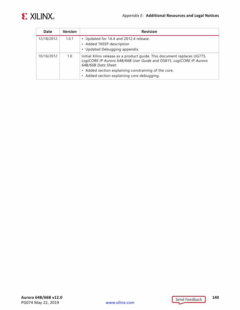
Aurora 64B/66B v12.0 140PG074 May 22, 2019 www.xilinx.com
Appendix E: Additional Resources and Legal Notices
12/18/2012 1.0.1 • Updated for 14.4 and 2012.4 release.• Added TKEEP description• Updated Debugging appendix.
10/16/2012 1.0 Initial Xilinx release as a product guide. This document replaces UG775, LogiCORE IP Aurora 64B/66B User Guide and DS815, LogiCORE IP Aurora 64B/66B Data Sheet.• Added section explaining constraining of the core.• Added section explaining core debugging.
Date Version Revision
Send Feedback
Aurora 64B/66B v12.0 141PG074 May 22, 2019 www.xilinx.com
Appendix E: Additional Resources and Legal Notices
Please Read: Important Legal NoticesThe information disclosed to you hereunder (the "Materials") is provided solely for the selection and use of Xilinx products. To the maximum extent permitted by applicable law: (1) Materials are made available "AS IS" and with all faults, Xilinx hereby DISCLAIMS ALL WARRANTIES AND CONDITIONS, EXPRESS, IMPLIED, OR STATUTORY, INCLUDING BUT NOT LIMITED TO WARRANTIES OF MERCHANTABILITY, NON-INFRINGEMENT, OR FITNESS FOR ANY PARTICULAR PURPOSE; and (2) Xilinx shall not be liable (whether in contract or tort, including negligence, or under any other theory of liability) for any loss or damage of any kind or nature related to, arising under, or in connection with, the Materials (including your use of the Materials), including for any direct, indirect, special, incidental, or consequential loss or damage (including loss of data, profits, goodwill, or any type of loss or damage suffered as a result of any action brought by a third party) even if such damage or loss was reasonably foreseeable or Xilinx had been advised of the possibility of the same. Xilinx assumes no obligation to correct any errors contained in the Materials or to notify you of updates to the Materials or to product specifications. You may not reproduce, modify, distribute, or publicly display the Materials without prior written consent. Certain products are subject to the terms and conditions of Xilinx's limited warranty, please refer to Xilinx's Terms of Sale which can be viewed at https://www.xilinx.com/legal.htm#tos; IP cores may be subject to warranty and support terms contained in a license issued to you by Xilinx. Xilinx products are not designed or intended to be fail-safe or for use in any application requiring fail-safe performance; you assume sole risk and liability for use of Xilinx products in such critical applications, please refer to Xilinx's Terms of Sale which can be viewed at https://www.xilinx.com/legal.htm#tos.AUTOMOTIVE APPLICATIONS DISCLAIMERAUTOMOTIVE PRODUCTS (IDENTIFIED AS “XA” IN THE PART NUMBER) ARE NOT WARRANTED FOR USE IN THE DEPLOYMENT OF AIRBAGS OR FOR USE IN APPLICATIONS THAT AFFECT CONTROL OF A VEHICLE (“SAFETY APPLICATION”) UNLESS THERE IS A SAFETY CONCEPT OR REDUNDANCY FEATURE CONSISTENT WITH THE ISO 26262 AUTOMOTIVE SAFETY STANDARD (“SAFETY DESIGN”). CUSTOMER SHALL, PRIOR TO USING OR DISTRIBUTING ANY SYSTEMS THAT INCORPORATE PRODUCTS, THOROUGHLY TEST SUCH SYSTEMS FOR SAFETY PURPOSES. USE OF PRODUCTS IN A SAFETY APPLICATION WITHOUT A SAFETY DESIGN IS FULLY AT THE RISK OF CUSTOMER, SUBJECT ONLY TO APPLICABLE LAWS AND REGULATIONS GOVERNING LIMITATIONS ON PRODUCT LIABILITY.© Copyright 2012–2019 Xilinx, Inc. Xilinx, the Xilinx logo, Artix, ISE, Kintex, Spartan, Virtex, Vivado, Zynq, and other designated brands included herein are trademarks of Xilinx in the United States and other countries. AMBA, AMBA Designer, Arm, ARM1176JZ-S, CoreSight, Cortex, PrimeCell, Mali, and MPCore are trademarks of Arm Limited in the EU and other countries.All other trademarks are the property of their respective owners.
Send Feedback


![Demonstration of a 16 Lane 10G Aurora 64B/66B Link on ......(UG476) [Ref 1] can be used to replicate the example design demo created in this application note. In this application note,](https://img.pdfslide.us/doc/110x75/60dbb610aff2f95a9c7b0f07/demonstration-of-a-16-lane-10g-aurora-64b66b-link-on-ug476-ref-1-can.jpg)