Embed Size (px)
Citation preview

SUPPLEMENTARY INFORMATIONDOI: 10.1038/NNANO.2014.150
NATURE NANOTECHNOLOGY | www.nature.com/naturenanotechnology 1
1
Atomically thin p-n junctions with van der Waals heterointerfaces
Chul-Ho Lee, Gwan-Hyoung Lee, Arend M. van der Zande, Wenchao Chen, Yilei Li,
Minyong Han, Xu Cui, Ghidewon Arefe, Colin Nuckolls, Tony F. Heinz, Jing Guo, James
Hone, and Philip Kim*
Table of contents
S1. Experimental methods (Fig. S1)
S2. Identification of the number of TMDC layers (Fig. S2)
S3. Device model simulation (Fig. S3)
S4. Electrical characteristics of a laterally metal-contacted p-n heterojunction in the dark (Figs. S4 and S5)
S5. Gate-tuneable photocurrent of a laterally metal-contacted p-n heterojunction (Fig. S6 and S7)
S6. Origin of photocurrent: Photovoltaic vs. Photo-thermoelectric effects
S7. Electrical characteristics of graphene-sandwiched p-n junctions with different thicknesses (Fig. S8)
S8. Spatially resolved photoresponses of graphene-sandwiched p-n junctions with different thicknesses (Fig. S9)
S9. Gate-tuneable photocurrent of graphene-sandwiched p-n junctions with different thicknesses (Fig. S10)
S10. Absorption spectra of the MoS2 / WSe2 heterostructure (Fig. S11)
S11. Excitation-power-dependent EQE measurements (Fig. S12)
References
Atomically thin p–n junctions with van der Waals heterointerfaces
© 2014 Macmillan Publishers Limited. All rights reserved.

2
S1. Experimental methods
We utilized two similar transfer procedures to fabricate van der Waals vertical p-n heterostructures. For preparing the stacks, we exfoliated monolayers from the bulk MoS2 (SPI Supplies) and WSe2 (Nanoscience Instruments) crystals.
Co-lamination & mechanical transfer technique for a vertical stack of MoS2 / WSe2 For the laterally metal-contacted p-n junction device (Fig. 1 and Fig. 2), we utilized a co-
lamination and mechanical transfer technique to fabricate the vertically stacked MoS2 / WSe2 heterostructure1,2. First, we used mechanical exfoliation with scotch tape to obtain monolayer WSe2 on a 280-nm-thick SiO2-coated Si substrate. Separately, we used mechanical
exfoliation to obtain monolayer MoS2 on a Si substrate coated with a polymer bilayer
consisting of thin water-soluble polyvinyl acetate (PVA) and 280-nm-thick
poly(methylmethacrylate) (PMMA). We released the PMMA film with MoS2 flakes from the
substrate by dissolving the PVA in water and transferred the film onto a polydimethyl siloxane (PDMS) stamp. Finally, we used a micromanipulator to place the MoS2 layer on top
of the WSe2 monolayer through an aligned transfer procedure1. This transfer process was
performed at a substrate temperature of 120 °C. After dissolving the PMMA in Acetone, we
fabricated electrical contacts using e-beam lithography. Importantly, we fabricated separate
contacts for the individual layers to minimize the Schottky barriers. Specifically, the MoS2
was contacted with Al / Cr / Au (40 / 1 / 50 nm) while the WSe2 was contacted with Pd / Au
(20 / 30 nm).
Van der Waals assembly of a graphene-sandwiched MoS2 / WSe2 heterostructure For the graphene-sandwiched p-n junction device (Fig. 3), we utilized a recently published
transfer technique utilizing the van der Waals adhesion of layers to “pickup” other layered
materials while avoiding use of polymers and solvents3. We started by exfoliating h-BN
layers with thickness of 10–30 nm on the ~1-μm-thick poly-propylene carbonate (PPC) film
on silicon, and separately exfoliating graphene and TMDC monolayers onto the SiO2 (280
nm) / Si substrates. We mechanically removed the PPC film with h-BN flakes from the Si substrate and placed the film onto a transparent elastomeric stamp (PDMS) fixed on a glass slide. To pick up the graphene layer (T-GR), we attached the inverted PDMS stamp to a micromanipulator and aligned the h-BN flake over a chosen exfoliated layer, brought the two flakes into contact, and then picked up the target graphene flake via a van der Waals interaction. This pick-up process was performed at a substrate temperature of 40 °C. The same process was repeated for the MoS2 and WSe2 layers to build the vertical p-n junction. Finally, we transferred the whole stack of h-BN / graphene / MoS2 / WSe2 on the PPC / PDMS stamp onto another graphene flake (B-GR) on the SiO2 / Si substrate by melting the PPC film at 90 °C, resulting in the van der Waals stack of h-BN / graphene / MoS2 / WSe2 / graphene on the SiO2 / Si substrate.
We used e-beam lithography to etch and add metal contacts to the heterostructures. First, we used PMMA/hydrogen silsesquioxane (HSQ) bilayer as an etch mask to define the junction in the transferred multi-stack. We performed a dry etch using an inductively coupled plasma etcher (Oxford ICP 80 system) with a mixture of O2 and CHF3 reactive gases. The typical etch rate was ~30 nm/min. After this process, we liftoff the PMMA / HSQ etch mask in acetone. We fabricated separate edge contacts by evaporating Cr / Pd / Au (10 / 15 / 50 nm) electrode to contact the top and bottom graphene layers (See Fig. S1)3.
© 2014 Macmillan Publishers Limited. All rights reserved.

3
Figure S1 | Fabrication of a graphene-sandwiched p-n heterojunction device. A series of optical images, representing each fabrication step for the graphene-sandwiched MoS2 / WSe2 monolayer device described in the main text (Fig. 3). In each optical image, the boundaries of individual atomic layers are indicated by the dashed lines.
Electrical and photocurrent measurements We performed electrical measurements by utilizing Keithley 2400 power supplies to
applying drain and gate voltages and a current amplifier (DL 1211) for current measurements.
The photocurrent measurements were carried out using three different methods. In Method 1, we exposed the sample to wide-field and broad spectrum light from a tungsten lamp through a microscope objective (10×). The data obtained in Fig. 2a utilized Method 1. Methods 2 and 3 utilized scanned photocurrent measurements using either a 532-nm cw laser (Crystalaser) or a supercontinum source (NKT photonics) with a monochrometer (7 nm FWHM). In both methods, the laser was focused down onto the sample through a objective (50×) to a ~ 0.7–1 m FWHM excitation spot. In Method 2, we performed scanning measurements using a scanned mechanical stage, while in Method 3, we performed scanning measurements using a confocal scanning laser setup. The data in Fig. 2b were obtained by Method 2, while the data in Fig. 3b were obtained by Method 3.
© 2014 Macmillan Publishers Limited. All rights reserved.
4
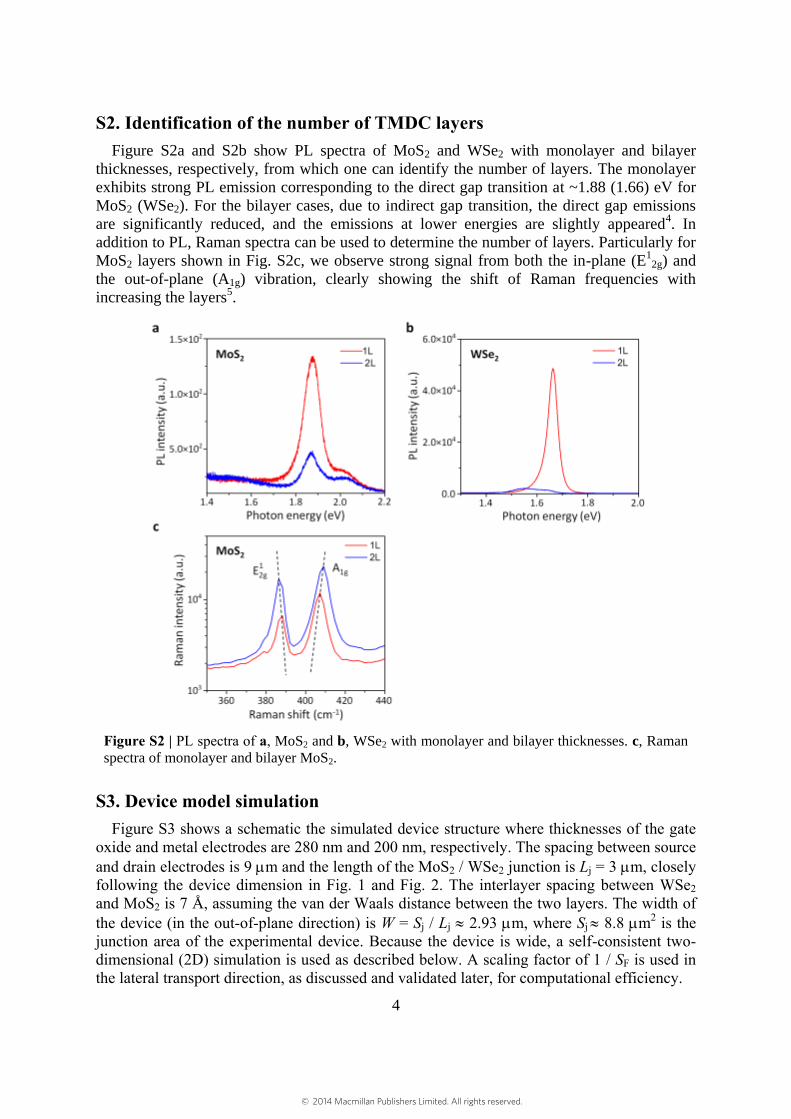
S2. Identification of the number of TMDC layers Figure S2a and S2b show PL spectra of MoS2 and WSe2 with monolayer and bilayer
thicknesses, respectively, from which one can identify the number of layers. The monolayer
exhibits strong PL emission corresponding to the direct gap transition at ~1.88 (1.66) eV for
MoS2 (WSe2). For the bilayer cases, due to indirect gap transition, the direct gap emissions
are significantly reduced, and the emissions at lower energies are slightly appeared4. In
addition to PL, Raman spectra can be used to determine the number of layers. Particularly for
MoS2 layers shown in Fig. S2c, we observe strong signal from both the in-plane (E1
2g) and
the out-of-plane (A1g) vibration, clearly showing the shift of Raman frequencies with
increasing the layers5.
Figure S2 | PL spectra of a, MoS2 and b, WSe2 with monolayer and bilayer thicknesses. c, Raman
spectra of monolayer and bilayer MoS2.
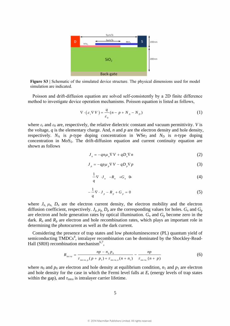
S3. Device model simulation Figure S3 shows a schematic the simulated device structure where thicknesses of the gate
oxide and metal electrodes are 280 nm and 200 nm, respectively. The spacing between source and drain electrodes is 9 m and the length of the MoS2 / WSe2 junction is Lj = 3 m, closely following the device dimension in Fig. 1 and Fig. 2. The interlayer spacing between WSe2 and MoS2 is 7 Å, assuming the van der Waals distance between the two layers. The width of the device (in the out-of-plane direction) is W = Sj / Lj 2.93 m, where Sj 8.8 m2 is the junction area of the experimental device. Because the device is wide, a self-consistent two-dimensional (2D) simulation is used as described below. A scaling factor of 1 / SF is used in the lateral transport direction, as discussed and validated later, for computational efficiency.
© 2014 Macmillan Publishers Limited. All rights reserved.
5
Figure S3 | Schematic of the simulated device structure. The physical dimensions used for model simulation are indicated.
Poisson and drift-diffusion equation are solved self-consistently by a 2D finite difference method to investigate device operation mechanisms. Poisson equation is listed as follows,
0
( )r A D
qV n p N N
(1)
where εr and ε0 are, respectively, the relative dielectric constant and vacuum permittivity. V is
the voltage, q is the elementary charge. And, n and p are the electron density and hole density,
respectively. NA is p-type doping concentration in WSe2 and ND is n-type doping
concentration in MoS2. The drift-diffusion equation and current continuity equation are
shown as follows
n n nJ qn V qD n (2)
p p pJ qp V qD p (3)
1
0n n n
J R Gq (4)
10
p p pJ R G
q (5)
where Jn, μn, Dn are the electron current density, the electron mobility and the electron
diffusion coefficient, respectively. Jp, μp, Dp are the corresponding values for holes. Gn and Gp
are electron and hole generation rates by optical illumination. Gn and Gp become zero in the
dark. Rn and Rp are electron and hole recombination rates, which plays an important role in
determining the photocurrent as well as the dark current.
Considering the presence of trap states and low photoluminescence (PL) quantum yield of
semiconducting TMDCs4, intralayer recombination can be dominated by the Shockley-Read-
Hall (SRH) recombination mechanism6,7
,
)(~
)()(,int1,int1,int
00
intpn
np
nnpp
pnnpR
ranrapra
ra
(6)
where n0 and p0 are electron and hole density at equilibrium condition, n1 and p1 are electron
and hole density for the case in which the Fermi level falls at Et (energy levels of trap states
within the gap), and τintra is intralayer carrier lifetime.
© 2014 Macmillan Publishers Limited. All rights reserved.

6
Meanwhile, interlayer recombination can be described by trap-assisted SRH or Coulomb-
interacting Langevin processes8, equations for two recombination mechanisms are expressed
as follows,
)(
~
i n t
,i n t
WMer
WM
SRHerpn
pnR
(7)
s
WMLerpBnR ~
,int (8)
where τinter is interlayer tunneling life time and B is Langevin recombination constant. Here s
is an exponent for modelling the behaviour of 2D systems9, which would be unity for the
3D case. We employed an exponent of s different from one only for holes (in WSe2), which
have a lower mobility than electrons (in MoS2). Note that the SRH recombination rate is
simplified because n0, p0, n1 and p1 are typically orders of magnitude lower than the values of
n and p. Also, the difference between τn and τp is neglected for simplicity, and differentiating
these two values does not change the qualitative conclusions.
It should be noted that drift-diffusion equations and current continuity equations are solved
in two individual monolayers (lateral direction) and their overlapped region (vertical
direction). In the lateral direction, we use mobility measured in individual monolayer devices
before the junction is formed. In the vertical direction, although interlayer transport is
dominated by quantum tunnelling, we used a phenomenological interlayer carrier mobility
µinter to describe the interlayer carrier transport between MoS2 and WSe2 monolayers,
int
/
/
t
er
av
E V a
(9)
where a is spacing between MoS2 and WSe2, V is voltage drop between two monolayer
materials, and τt is the tunneling time between two layers. The value of V can be
approximately set as the difference between the conduction (valence) band edge of MoS2 and
valence (conduction) band of WSe2 divided by elementary charge for electron (hole)
transport. Numerical calculation shows that the value varies about 10 % in the bias range of
interest. Note that phenomenological mobility used in our simulation results in faster
interlayer charge transfer rate than intralayer recombination rate as expected from
experimental observation of strong PL quenching in the MoS2 / WSe2 heterojunction.
Because the large aspect ratio between the lateral size and the vertical interlayer distance,
numerical challenges need to be taken care of in the simulation. We developed and validated
a scaling method, which scales down the dimension in the transport direction by a scaling
factor of 1 / SF to reduce computational cost. The intralayer mobility in the horizontal
direction is scaled down by factor 1 / SF to maintain same parasitic resistance. The
recombination and generation rates are scaled up by factor SF to maintain same current per
unit width. The phenomenological interlayer mobility is scaled up by a factor of SF. We have
numerically tested that the physical quantities of interest, including the dark and
photoresponse I–V characteristics of the junction and the charge density in the junction region,
are insensitive to the scaling factor if SF 30. The electrostatic screening length in the
horizontal direction is considerably shorter than 100 nm due to atomic thickness of WSe2 and
MoS2. To further speed up simulation, a non-uniform numerical grid is used in the vertical
direction for the numerical solution of Poisson equation.
© 2014 Macmillan Publishers Limited. All rights reserved.

7
S4. Electrical characteristics of a laterally metal-contacted p-n
heterojunction in the dark
Figure S4 presents band diagrams in the lateral direction under reverse (Vds = - 0.6 V), zero (0 V), forward (0.6 V) biases at Vg = 0 V, respectively. At a reverse bias, holes in p-doped WSe2 and electrons in n-doped MoS2 are depleted, and the quasi-Fermi level of MoS2 in the non-overlapped region is close to the conduction band edge, and that of WSe2 is close to the valence band edge. Depletion in the junction region and quasi-Fermi level splitting at the reverse bias results in large band bending between overlapped and non-overlapped regions in the lateral direction. On the other hand, at a forward bias, both holes in p-doped WSe2 and electrons in n-doped MoS2 are accumulated. Therefore, band bending in the lateral direction is negligibly small as shown in the bottom panel of Fig. S4 as well as in Fig. 1c.
Figure S4 | Band diagrams in the lateral transport direction at different biases, obtained from model simulation considering electrostatics. (top panel: Vds = -0.6 V, middle panel: 0 V, bottom panel: 0.6 V)
Due to lack of a depletion region, charge transport in an atomically thin junction is
governed by interlayer recombination processes between two majority carriers accumulated
in each layer, and thus I–V curves do not show an exponential characteristic even for an ideal junction. In our model simulation, we examined two recombination mechanisms described above. Figure S5 shows comparison of experimental and theoretical dark I–V curves at Vg = 0 V. Both SRH and Langevin mechanisms show good agreements with the experimental data. For quantitative matching, we estimated the interlayer tunneling life time (τt) of 40 s and Langevin recombination constant (B) of 1.67 × 10⁻¹³ m2/s for s = 1, 8.33 × 10⁻¹⁷ m2/s for s = 1.2, and 9.17 × 10⁻²² m2/s for s = 1.5.
© 2014 Macmillan Publishers Limited. All rights reserved.

8
Figure S5 | Comparison of the measured and the simulated I–V curves in the dark at Vg = 0 V. In our model simulation, both SRH and Langevin mechanisms are considered, showing good agreements with the measured I–V curve.
Unlike an ideal case in simulation, in real devices, parasitic resistances are likely to exist in both metal (Pd)-WSe2 and metal (Al)-MoS2 contacts, as well as lateral charge transport in WSe2 and MoS2 monolayers. We indeed found that the simulated I–V characteristics are sensitive to the parasitic resistance, which can reduce the splitting of quasi-Fermi-energy levels of majority carriers in the overlapped junction region and thereby results in lower majority carrier densities. For example, the forward bias current decreases when we include the Schottky barrier of 0.3 eV at the Pd-WSe2 junction. Consequently, we estimated smaller tunnelling lifetime (~microsecond time scale (> 1 s)) and larger Langevin recombination constant (~2.0 × 10⁻¹⁰ m2/s for s = 1.0), in order to obtain the forward bias current measured in our device. Although it is very difficult to get a quantitative number precisely, it should be noted that the microsecond time sale obtained here is much longer than those of any other competing processes including intralayer radiative (or nonradiative) recombination rate and charge transfer rate (for exciton dissociation) as discussed in the main text10.
S5. Gate-tuneable photocurrent of a laterally metal-contacted p-n heterojunction
The modulation of interlayer tunneling recombination rate while varying the gate voltage leads to the gate-tuneable photocurrent as discussed in the main text. As shown in Fig. 2f, for both SRH and Langevin mechanisms, the recombination rate is minimized near Vg = 0 V, resulting in the maximum photocurrent under a constant photogeneration rate. The recombination rate increases as varying the gate voltage to either polarity due to accumulation of one type of majority carrier.
We performed detailed simulations for modeling of the 2D Langevin recombination rate (R = BnMpW
s) with different exponent values of s = 1.0, 1.2, and 1.5. The value of s = 1.0 corresponds to the 3D case, while s = 1.2 and s = 1.5 represent lower and upper bounds for the 2D case9. B is a density-independent parameter chosen for each value of s. Note that the recombination rate shows a superlinear dependence on hole density in the 2D Langevin
© 2014 Macmillan Publishers Limited. All rights reserved.

9
model, while it depends linearly on hole density for the 3D case. Figure 6 shows simulated curves for the gate-dependent photocurrent for the different choices of s. The results indicate that the sharply peaked photoresponse is preserved, although different values for s change the quantitative features. In the 2D modeling, the simulated curves showed discrepancies, particularly for Vg < 0 V since the hole density increases. We believe that Langevin rate may be the dominant mechanism in view of the enhanced Coulomb interaction between electrons and holes in this confined 2D system. However, we cannot exclude SRH recombination because of the potential role of imperfections at the junction interface, as well as defects in the materials. Indeed, the two recombination processes may coexist in the device.
Figure S6 | Measured and simulated photocurrent response (for Vds = 0 V) as a function of gate voltage. The simulations were performed for the Langevin model with exponents of s = 1, 1.2, and 1.5.
© 2014 Macmillan Publishers Limited. All rights reserved.
10
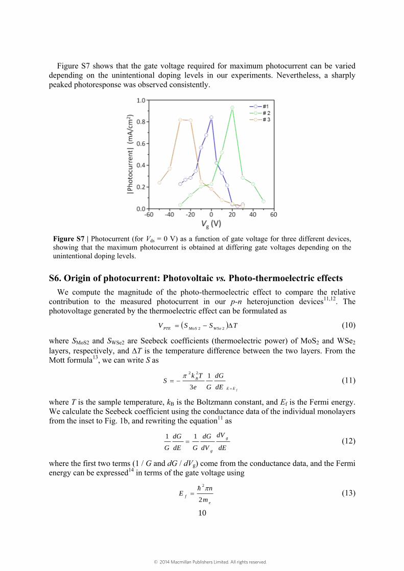
Figure S7 shows that the gate voltage required for maximum photocurrent can be varied depending on the unintentional doping levels in our experiments. Nevertheless, a sharply peaked photoresponse was observed consistently.
Figure S7 | Photocurrent (for Vds = 0 V) as a function of gate voltage for three different devices, showing that the maximum photocurrent is obtained at differing gate voltages depending on the unintentional doping levels.
S6. Origin of photocurrent: Photovoltaic vs. Photo-thermoelectric effects We compute the magnitude of the photo-thermoelectric effect to compare the relative
contribution to the measured photocurrent in our p-n heterojunction devices11,12. The photovoltage generated by the thermoelectric effect can be formulated as
TSSVWSeMoSPTE
22
(10)
where SMoS2 and SWSe2 are Seebeck coefficients (thermoelectric power) of MoS2 and WSe2 layers, respectively, and T is the temperature difference between the two layers. From the Mott formula13, we can write S as
fEE
B
dE
dG
Ge
TkS
1
3
22 (11)
where T is the sample temperature, kB is the Boltzmann constant, and Ef is the Fermi energy. We calculate the Seebeck coefficient using the conductance data of the individual monolayers from the inset to Fig. 1b, and rewriting the equation11 as
dE
dV
dV
dG
GdE
dG
G
g
g
11 (12)
where the first two terms (1 / G and dG / dVg) come from the conductance data, and the Fermi energy can be expressed14 in terms of the gate voltage using
e
fm
nE
2
2
(13)
© 2014 Macmillan Publishers Limited. All rights reserved.

11
0
1VVC
en
gg (14)
where n is the density of electrons/holes in the material, me = 0.35m0×mh = 0.428m0 is the electron/hole mass at the k point (using the numbers for MoS2 only), and Cg = 1.23 × 10⁻⁴ F∙m-2 is the capacitance per unit area of a back-gated 2D material on a 280-nm-thick SiO2 / Si substrate. With these numbers, we compute the Seebeck coefficient of two TMDC monolayers at Vg = 0 V as SMoS2 ~ -3.3 mV/K and SWSe2 ~ 4.5 mV/K. Then, total contribution becomes to be S ~ -7.8 mV/K.
Since we do not have a good measure for thermal conductivity across a disparate van der Waals interface, it is difficult to compute the temperature difference in our samples. However, at the ~ 1–5 W powers used in our measurements, it is very unlikely to be above 1 K11,12,15,16. If we compare the value of the photothermal voltage (< 10 mV) to the measured open-circuit voltage of 500–700 mV, it is clear that the photothermal contribution is small compared to the photovoltaic effect. This calculation was performed for the vertical MoS2 / WSe2 junction, however the Seebeck coefficients will not change drastically for the laterally-contacted heterojunction, so the contribution should be small in all geometries studied here.
S7. Electrical characteristics of graphene-sandwiched p-n junctions with different thicknesses
The photoresponse I–V characteristics of graphene-sandwiched p-n junctions are modelled by a simple circuit model as shown in Fig. S8a. Rs and Rt are series resistance and the tunnelling resistance between the top and bottom graphene contacts, respectively. I0 is current source related to photogenerated current. Despite simplicity of the model, it explains the qualitative features of the I–V characteristics depending on the number of layers as shown in Fig. S8b.
The shunt resistance is due to tunneling between two graphene contacts separated by the atomically thin p-n junction. Since tunnelling current is exponentially dependent on tunnelling distance, the shunt resistance exponentially depends on the number of layers as shown below,
0
N
tR R e (10)
where N is number of layers. By carefully choosing parameters, we can get the simulation results with a quantitative agreement to experimental measurements. The parameters used are
4
05 10 ( )
N s NR I R I V
and
0/ 10
NI I , where IN is a normalization current. The diode
shows the I–V characteristic same as the multilayer p-n junction in the dark, but with a normalization unit that results in I (at V = 0.7 V) / IN 80. Piecewise function is used to fit the dark I–V characteristics. The simple model captures the qualitative features of the nearly linear I–V characteristics of the monolayer junction, the increase of the open-circuit voltage and the transition to the diode-like I–V with increasing the number of layers.
© 2014 Macmillan Publishers Limited. All rights reserved.

12
Figure S8 | a. Circuit diagram for modelling the graphene-sandwiched p-n heterojunction device, where the series resistance (Rs) and shunt tunneling resistance (Rt) are included. b. Simulated I–V curves of the graphene-sandwiched p-n heterojunctions with different thicknesses described in the main text (Fig. 3d).
S8. Spatially resolved photoresponses of graphene-sandwiched p-n junctions with different thicknesses
Figure S9 shows optical images and corresponding photocurrent maps for graphene-
sandwiched bilayer and multilayer junction devices. Photocurrent is uniformly observed in
the entire junction region where two active TMDC layers overlap with top and bottom
graphene contact layers.
Figure S9 | Optical images and corresponding photocurrent maps (at Vds = 0 V) of the graphene-sandwiched p-n junctions consisting of bilayer-bilayer (2L-2L) and multilayer-multilayer (ML-ML (10-9 nm)). The junction areas and metal electrodes are indicated by the dashed and solid lines, respectively.
© 2014 Macmillan Publishers Limited. All rights reserved.
13
S9. Gate-tuneable photocurrent of graphene-sandwiched p-n junctions with different thicknesses
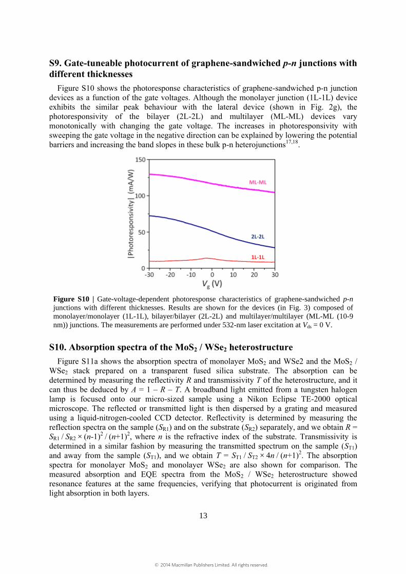
Figure S10 shows the photoresponse characteristics of graphene-sandwiched p-n junction devices as a function of the gate voltages. Although the monolayer junction (1L-1L) device exhibits the similar peak behaviour with the lateral device (shown in Fig. 2g), the photoresponsivity of the bilayer (2L-2L) and multilayer (ML-ML) devices vary monotonically with changing the gate voltage. The increases in photoresponsivity with sweeping the gate voltage in the negative direction can be explained by lowering the potential barriers and increasing the band slopes in these bulk p-n heterojunctions17,18.
Figure S10 | Gate-voltage-dependent photoresponse characteristics of graphene-sandwiched p-n
junctions with different thicknesses. Results are shown for the devices (in Fig. 3) composed of
monolayer/monolayer (1L-1L), bilayer/bilayer (2L-2L) and multilayer/multilayer (ML-ML (10-9
nm)) junctions. The measurements are performed under 532-nm laser excitation at Vds = 0 V.
S10. Absorption spectra of the MoS2 / WSe2 heterostructure Figure S11a shows the absorption spectra of monolayer MoS2 and WSe2 and the MoS2 /
WSe2 stack prepared on a transparent fused silica substrate. The absorption can be determined by measuring the reflectivity R and transmissivity T of the heterostructure, and it can thus be deduced by A = 1 – R – T. A broadband light emitted from a tungsten halogen lamp is focused onto our micro-sized sample using a Nikon Eclipse TE-2000 optical microscope. The reflected or transmitted light is then dispersed by a grating and measured using a liquid-nitrogen-cooled CCD detector. Reflectivity is determined by measuring the reflection spectra on the sample (SR1) and on the substrate (SR2) separately, and we obtain R = SR1 / SR2 × (n-1)2
/ (n+1)2, where n is the refractive index of the substrate. Transmissivity is determined in a similar fashion by measuring the transmitted spectrum on the sample (ST1) and away from the sample (ST1), and we obtain T = ST1 / ST2 × 4n / (n+1)2. The absorption spectra for monolayer MoS2 and monolayer WSe2 are also shown for comparison. The measured absorption and EQE spectra from the MoS2 / WSe2 heterostructure showed resonance features at the same frequencies, verifying that photocurrent is originated from light absorption in both layers.
© 2014 Macmillan Publishers Limited. All rights reserved.

14
Since the absorption spectrum of a layered material strongly depends on the substrate used, we further performed simulation for the MoS2 / WSe2 heterostructures on the 280-nm-thick SiO2 coated Si substrates. Figure S11b shows the simulated absorption spectra from the
monolayer and multilayer MoS2 / WSe2 heterostructures. To do that, we extracted the
dielectric function of the heterojunction from the measured absorption spectrum for the
monolayer heterojunction, and used those values of bulk MoS2 and WSe2 crystals for the
multilayer one19
. By taking into account the substrate interference effect, we then simulate
the absorption spectra for two different thicknesses. Both absorption spectra showed the
resonance peaks corresponding to excitonic transitions of two materials. However, for the
multilayer heterostructure, the peaks became broader than those of the monolayer case
because of the reduced lifetime.
Figure S11 | a. Absorption spectra for monolayer WSe2, monolayer MoS2 and the MoS2 / WSe2
heterostructure, measured from the samples prepared on a fused silica substrate. The featured
absorption peaks of individual MoS2 and WSe2 monolayers are also observed in the spectrum of the
heterostructure. b. Simulated absorption spectra for the monolayer MoS2 / WSe2 heterostructure
and the multilayer MoS2 / WSe2 (10 / 9 nm) heterostructure on the SiO2 (280 nm) / Si substrate.
© 2014 Macmillan Publishers Limited. All rights reserved.

15
S11. Excitation-power-dependent EQE measurements Figure S12 shows the measured values of EQE as a function of excitation laser power for
graphene-sandwiched p-n junction devices. Irrespective of junction thickness, the devices
exhibit the linear photoresponse up to the power of ~10 W, leading to almost constant EQE
values. However, the EQE decreases as the excitation power increases above the critical
values.
Figure S12 | EQE plots as a function of excitation power for graphene-sandwiched p-n
heterojunctions. Three devices described here include monolayer/monolayer (1L-1L),
bilayer/bilayer (2L-2L) and multilayer/multilayer (ML-ML (10-9 nm)) junctions. For the
measurements, a 532-nm laser was used as an excitation source.
References 1. Dean, C. R. et al. Boron nitride substrates for high-quality graphene electronics. Nature
Nanotech. 5, 722-726 (2010).
2. Lee, G.-H. et al. Flexible and transparent MoS2 field-effect transistors on hexagonal
boron nitride-graphene heterostructures. ACS Nano 9, 7931-7936 (2013).
3. Wang, L. et al. One-dimensional electrical contact to a two-dimensional material.
Science 342, 614-617 (2013).
4. Mak, K. F., Lee, C., Hone, J., Shan, J. & Heinz, T. F. Atomically thin MoS2: A new
direct-gap semiconductor. Phys. Rev. Lett. 105, 136805 (2010).
5. Lee, C. et al. Anomalous lattice vibrations of single- and few-layer MoS2. ACS Nano 4,
2695-2700 (2010).
6. Hall, R. N. Electron-hole recombination in Germanium. Phys. Rev. 87, 387-387 (1952).
7. Shockley, W. & Read, W. T. Statistics of the recombinations of holes and electrons. Phys.
Rev. 87, 835-842 (1952).
8. Langevin, P. Recombination et mobilité des ions dans les gaz. Ann. Chim. Phys. 28, 433-
531 (1903).
9. Greenham, N. C. & Bobbert, P. A. Two-dimensional electron-hole capture in a
disordered hopping system. Phys. Rev. B 68, 245301 (2003).
10. Shi, H. Y. et al. Exciton dynamics in suspended mono layer and few-layer MoS2 2D
crystals. ACS Nano 7, 1072-1080 (2013).
© 2014 Macmillan Publishers Limited. All rights reserved.
16
11. Xu, X. D., Gabor, N. M., Alden, J. S., van der Zande, A. M. & McEuen, P. L. Photo-
thermoelectric effect at a graphene interface junction. Nano. Lett. 10, 562-566 (2010).
12. Gabor, N. M. et al. Hot carrier-assisted intrinsic photoresponse in graphene. Science
334, 648-652 (2011).
13. Ashcroft, N. W. & Mermin, N. D. Solid state physics, (Tomson Learning Inc., London,
UK, 1976).
14. Mak, K. F. et al. Tightly bound trions in monolayer MoS2. Nature Mater. 12, 207-211
(2013).
15. Balandin, A. A. et al. Superior thermal conductivity of single-layer graphene. Nano.
Lett. 8, 902-907 (2008).
16. Buscema, M. et al. Large and tunable photothermoelectric effect in single-layer MoS2.
Nano. Lett. 13, 358-363 (2013).
17. Britnell, L. et al. Strong light-matter interactions in heterostructures of atomically thin
films. Science 340, 1311-1314 (2013).
18. Yu, W. J. et al. Highly efficient gate-tunable photocurrent generation in vertical
heterostructures of layered materials. Nature Nanotech. 8, 952-958 (2013).
19. Beal, A. R. & Hughes, H. P. Kramers-Kronig analysis of the reflectivity spectra of 2H-
MoS2, 2H-MoSe2 and 2H-MoTe2. J. Phys. C. 12, 881-890 (1979).
© 2014 Macmillan Publishers Limited. All rights reserved.