Embed Size (px)
Citation preview

Features• High Performance, Low Power Atmel®AVR® 8-bit Microcontroller• Advanced RISC Architecture
– 131 Powerful Instructions - Most Single Clock Cycle Execution– 32 × 8 General Purpose Working Registers– Fully Static Operation– Up to 1 MIPS throughput per MHz– On-chip 2-cycle Multiplier
• Data and Non-Volatile Program Memory– 16/32/64K Bytes Flash of In-System Programmable Program Memory– 512B/1K/2K Bytes of In-System Programmable EEPROM– 1/2/4K Bytes Internal SRAM– Write/Erase Cycles: 10,000 Flash/ 100,000 EEPROM– Data Retention: 20 years at 85°C/ 100 years at 25°C(1)
– Optional Boot Code Section with Independent Lock BitsIn-System Programming by On-chip Boot ProgramTrue Read-While-Write Operation
– Programming Lock for Flash Program and EEPROM Data Security• On Chip Debug Interface (debugWIRE)• CAN 2.0A/B with 6 Message Objects - ISO 16845 Certified• LIN 2.1 and 1.3 Controller or 8-Bit UART• One 12-bit High Speed PSC (Power Stage Controller)
– Non Overlapping Inverted PWM Output Pins With Flexible Dead-Time– Variable PWM duty Cycle and Frequency– Synchronous Update of all PWM Registers– Auto Stop Function for Emergency Event
• Peripheral Features– One 8-bit General purpose Timer/Counter with Separate Prescaler, Compare Mode
and Capture Mode– One 16-bit General purpose Timer/Counter with Separate Prescaler, Compare
Mode and Capture Mode– One Master/Slave SPI Serial Interface– 10-bit ADC
Up To 11 Single Ended Channels and 3 Fully Differential ADC Channel PairsProgrammable Gain (5×, 10×, 20×, 40×) on Differential ChannelsInternal Reference VoltageDirect Power Supply Voltage Measurement
– 10-bit DAC for Variable Voltage Reference (Comparators, ADC)– Four Analog Comparators with Variable Threshold Detection– 100µA ±2% Current Source (LIN Node Identification)– Interrupt and Wake-up on Pin Change– Programmable Watchdog Timer with Separate On-Chip Oscillator– On-chipTemperature Sensor
• Special Microcontroller Features– Low Power Idle, Noise Reduction, and Power Down Modes– Power On Reset and Programmable Brown Out Detection– In-System Programmable via SPI Port– High Precision Crystal Oscillator for CAN Operations (16MHz)– Internal Calibrated RC Oscillator ( 8MHz)– On-chip PLL for fast PWM ( 32MHz, 64MHz) and CPU (16MHz)
• Operating Voltage: 2.7V - 5.5V• Extended Operating Temperature:
– -40°C to +85°C• Core Speed Grade:
– 0 - 8MHz @ 2.7 - 4.5V– 0 - 16MHz @ 4.5 - 5.5V
8209DS–AVR–11/10
8-bit Microcontroller with 16/32/64K Bytes In-SystemProgrammable Flash
ATmega16M1ATmega32M1ATmega64M1
PreliminarySummary

28209DS–AVR–11/10
ATmega16M1/32M1/64M1
1. Pin Configurations
Figure 1-1. ATmega16M1/32M1/64M1 TQFP32/QFN32 (7 × 7 mm) Package.
12345678
2423222120191817
(PCINT18/PSCIN2/OC1A/MISO_A) PD2(PCINT19/TXD/TXLIN/OC0A/SS/MOSI_A) PD3
(PCINT9/PSCIN1/OC1B/SS_A) PC1VCCGND
(PCINT10/T0/TXCAN) PC2(PCINT11/T1/RXCAN/ICP1B) PC3(PCINT0/MISO/PSCOUT2A) PB0
PB4 (AMP0+/PCINT4) PB3 (AMP0-/PCINT3)PC6 (ADC10/ACMP1/PCINT14)AREF(ISRC)AGNDAVCCPC5 (ADC9/ACMP3/AMP1+/PCINT13)PC4 (ADC8/ACMPN3/AMP1-/PCINT12)
32
31
30
29
28
27
26
25
9 10
11
12
13
14
15
16
(PC
INT
1/M
OS
I/PS
CO
UT
2B)
PB
1(P
CIN
T25
/OC
0B/X
TAL1
) P
E1
(PC
INT
26/A
DC
0/X
TAL2
) P
E2
(PC
INT
20/A
DC
1/R
XD
/RX
LIN
/ICP
1A/S
CK
_A)
PD
4(A
DC
2/A
CM
P2/
PC
INT
21)
PD
5 (
AD
C3/
AC
MP
N2/
INT
0/P
CIN
T22
) P
D6
(A
CM
P0/
PC
INT
23)
PD
7
(A
DC
5/IN
T1/
AC
MP
N0/
PC
INT
2) P
B2
PD
1(P
CIN
T17
/PS
CIN
0/C
LKO
)P
E0 (
PC
INT
24/R
ES
ET
/OC
D)
PC
0(P
CIN
T8/
INT
3/P
SC
OU
T1A
) P
D0 (
PC
INT
16/P
SC
OU
T0A
)P
B7
(AD
C4/
PS
CO
UT
0B/S
CK
/PC
INT
7)P
B6
(AD
C7/
PS
CO
UT
1B/P
CIN
T6)
PB
5 (A
DC
6/IN
T2/
AC
MP
N1/
AM
P2-
/PC
INT
5)
PC
7 (D
2A/A
MP
2+/P
CIN
T15
)
38209DS–AVR–11/10
ATmega16M1/32M1/64M1
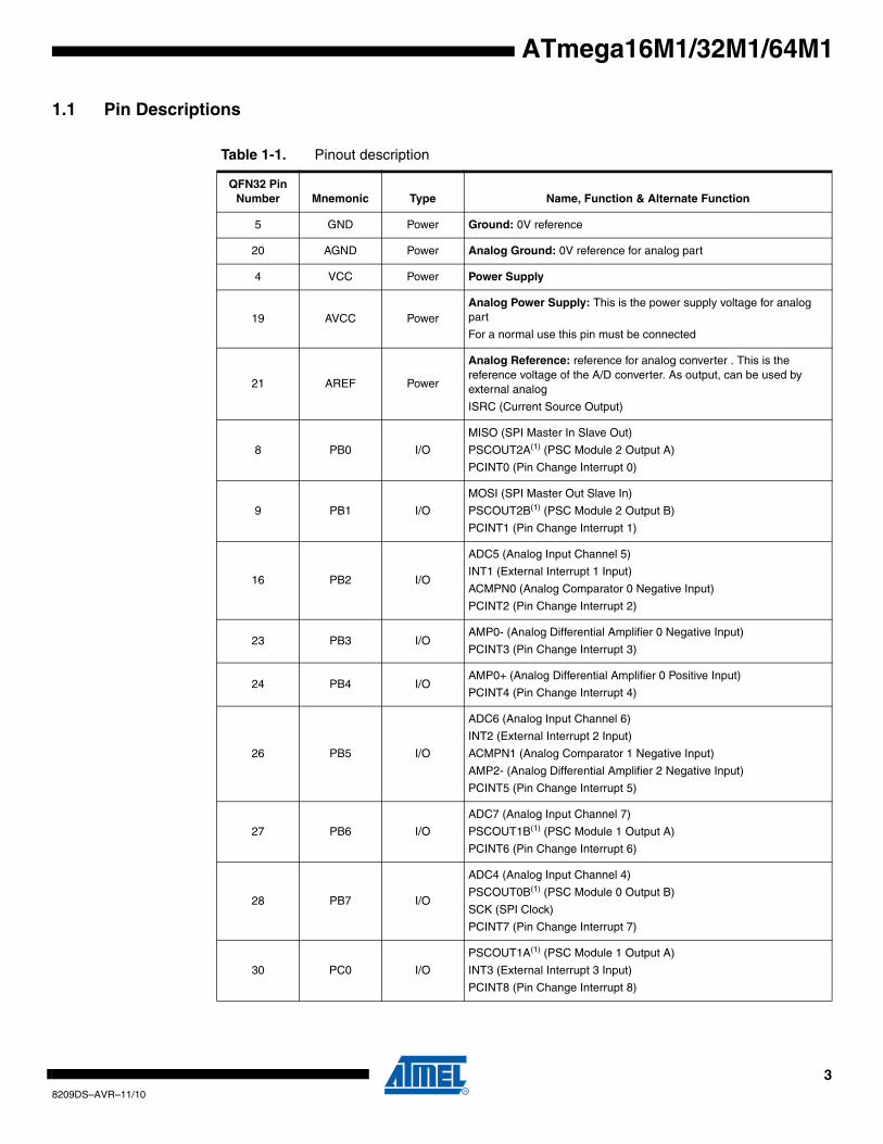
1.1 Pin Descriptions
Table 1-1. Pinout description
QFN32 Pin Number Mnemonic Type Name, Function & Alternate Function
5 GND Power Ground: 0V reference
20 AGND Power Analog Ground: 0V reference for analog part
4 VCC Power Power Supply
19 AVCC PowerAnalog Power Supply: This is the power supply voltage for analog part
For a normal use this pin must be connected
21 AREF Power
Analog Reference: reference for analog converter . This is the reference voltage of the A/D converter. As output, can be used by external analog
ISRC (Current Source Output)
8 PB0 I/O
MISO (SPI Master In Slave Out)
PSCOUT2A(1) (PSC Module 2 Output A)
PCINT0 (Pin Change Interrupt 0)
9 PB1 I/O
MOSI (SPI Master Out Slave In)
PSCOUT2B(1) (PSC Module 2 Output B)
PCINT1 (Pin Change Interrupt 1)
16 PB2 I/O
ADC5 (Analog Input Channel 5)
INT1 (External Interrupt 1 Input)
ACMPN0 (Analog Comparator 0 Negative Input)
PCINT2 (Pin Change Interrupt 2)
23 PB3 I/OAMP0- (Analog Differential Amplifier 0 Negative Input)
PCINT3 (Pin Change Interrupt 3)
24 PB4 I/OAMP0+ (Analog Differential Amplifier 0 Positive Input)
PCINT4 (Pin Change Interrupt 4)
26 PB5 I/O
ADC6 (Analog Input Channel 6)
INT2 (External Interrupt 2 Input)
ACMPN1 (Analog Comparator 1 Negative Input)
AMP2- (Analog Differential Amplifier 2 Negative Input)
PCINT5 (Pin Change Interrupt 5)
27 PB6 I/O
ADC7 (Analog Input Channel 7)
PSCOUT1B(1) (PSC Module 1 Output A)
PCINT6 (Pin Change Interrupt 6)
28 PB7 I/O
ADC4 (Analog Input Channel 4)
PSCOUT0B(1) (PSC Module 0 Output B)
SCK (SPI Clock)
PCINT7 (Pin Change Interrupt 7)
30 PC0 I/O
PSCOUT1A(1) (PSC Module 1 Output A)
INT3 (External Interrupt 3 Input)
PCINT8 (Pin Change Interrupt 8)
48209DS–AVR–11/10
ATmega16M1/32M1/64M1
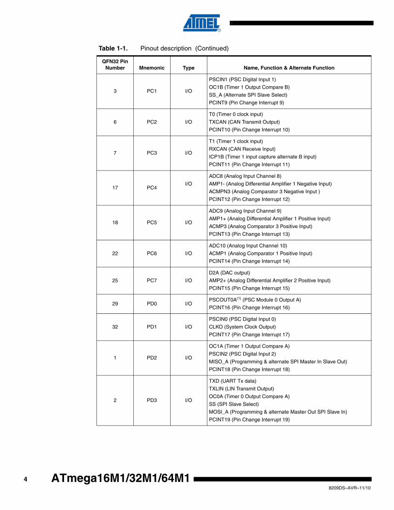
3 PC1 I/O
PSCIN1 (PSC Digital Input 1)
OC1B (Timer 1 Output Compare B)
SS_A (Alternate SPI Slave Select)
PCINT9 (Pin Change Interrupt 9)
6 PC2 I/O
T0 (Timer 0 clock input)
TXCAN (CAN Transmit Output)
PCINT10 (Pin Change Interrupt 10)
7 PC3 I/O
T1 (Timer 1 clock input)
RXCAN (CAN Receive Input)
ICP1B (Timer 1 input capture alternate B input)
PCINT11 (Pin Change Interrupt 11)
17 PC4I/O
ADC8 (Analog Input Channel 8)
AMP1- (Analog Differential Amplifier 1 Negative Input)
ACMPN3 (Analog Comparator 3 Negative Input )
PCINT12 (Pin Change Interrupt 12)
18 PC5 I/O
ADC9 (Analog Input Channel 9)
AMP1+ (Analog Differential Amplifier 1 Positive Input)
ACMP3 (Analog Comparator 3 Positive Input)
PCINT13 (Pin Change Interrupt 13)
22 PC6 I/O
ADC10 (Analog Input Channel 10)
ACMP1 (Analog Comparator 1 Positive Input)
PCINT14 (Pin Change Interrupt 14)
25 PC7 I/O
D2A (DAC output)
AMP2+ (Analog Differential Amplifier 2 Positive Input)
PCINT15 (Pin Change Interrupt 15)
29 PD0 I/OPSCOUT0A(1) (PSC Module 0 Output A)
PCINT16 (Pin Change Interrupt 16)
32 PD1 I/O
PSCIN0 (PSC Digital Input 0)
CLKO (System Clock Output)
PCINT17 (Pin Change Interrupt 17)
1 PD2 I/O
OC1A (Timer 1 Output Compare A)
PSCIN2 (PSC Digital Input 2)
MISO_A (Programming & alternate SPI Master In Slave Out)
PCINT18 (Pin Change Interrupt 18)
2 PD3 I/O
TXD (UART Tx data)
TXLIN (LIN Transmit Output)
OC0A (Timer 0 Output Compare A)
SS (SPI Slave Select)
MOSI_A (Programming & alternate Master Out SPI Slave In)
PCINT19 (Pin Change Interrupt 19)
Table 1-1. Pinout description (Continued)
QFN32 Pin Number Mnemonic Type Name, Function & Alternate Function

58209DS–AVR–11/10
ATmega16M1/32M1/64M1
Note: 1. Only for Atmega32M1/64M1
2. On the engineering samples, the ACMPN3 alternate function is not located on PC4. It is located on PE2
2. OverviewThe ATmega16M1/32M1/64M1 is a low-power CMOS 8-bit microcontroller based on the AVRenhanced RISC architecture. By executing powerful instructions in a single clock cycle, theATmega16M1/32M1/64M1 achieves throughputs approaching 1 MIPS per MHz allowing thesystem designer to optimize power consumption versus processing speed.
12 PD4 I/O
ADC1 (Analog Input Channel 1)
RXD (UART Rx data)
RXLIN (LIN Receive Input)
ICP1A (Timer 1 input capture alternate A input)
SCK_A (Programming & alternate SPI Clock)
PCINT20 (Pin Change Interrupt 20)
13 PD5 I/O
ADC2 (Analog Input Channel 2)
ACMP2 (Analog Comparator 2 Positive Input)
PCINT21 (Pin Change Interrupt 21)
14 PD6 I/O
ADC3 (Analog Input Channel 3)
ACMPN2 (Analog Comparator 2 Negative Input)
INT0 (External Interrupt 0 Input)
PCINT22 (Pin Change Interrupt 22)
15 PD7 I/OACMP0 (Analog Comparator 0 Positive Input)
PCINT23 (Pin Change Interrupt 23)
31 PE0 I/O or I
RESET (Reset Input)
OCD (On Chip Debug I/O)
PCINT24 (Pin Change Interrupt 24)
10 PE1 I/O
XTAL1 (XTAL Input)
OC0B (Timer 0 Output Compare B)
PCINT25 (Pin Change Interrupt 25)
11 PE2 I/O
XTAL2 (XTAL Output)
ADC0 (Analog Input Channel 0)
PCINT26 (Pin Change Interrupt 26)
Table 1-1. Pinout description (Continued)
QFN32 Pin Number Mnemonic Type Name, Function & Alternate Function
68209DS–AVR–11/10
ATmega16M1/32M1/64M1
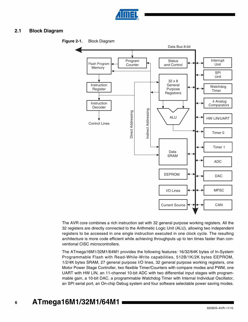
2.1 Block Diagram
Figure 2-1. Block Diagram
The AVR core combines a rich instruction set with 32 general purpose working registers. All the32 registers are directly connected to the Arithmetic Logic Unit (ALU), allowing two independentregisters to be accessed in one single instruction executed in one clock cycle. The resultingarchitecture is more code efficient while achieving throughputs up to ten times faster than con-ventional CISC microcontrollers.
The ATmega16M1/32M1/64M1 provides the following features: 16/32/64K bytes of In-SystemProgrammable Flash with Read-While-Write capabilities, 512B/1K/2K bytes EEPROM,1/2/4K bytes SRAM, 27 general purpose I/O lines, 32 general purpose working registers, oneMotor Power Stage Controller, two flexible Timer/Counters with compare modes and PWM, oneUART with HW LIN, an 11-channel 10-bit ADC with two differential input stages with program-mable gain, a 10-bit DAC, a programmable Watchdog Timer with Internal Individual Oscillator,an SPI serial port, an On-chip Debug system and four software selectable power saving modes.
Flash ProgramMemory
InstructionRegister
InstructionDecoder
ProgramCounter
Control Lines
32 x 8GeneralPurpose
Registrers
ALU
Statusand Control
I/O Lines
EEPROM
Data Bus 8-bit
DataSRAM
Dire
ct A
ddre
ssin
g
Indi
rect
Add
ress
ing
InterruptUnit
SPIUnit
WatchdogTimer
4 AnalogComparators
DAC
ADC
MPSC
Timer 1
Timer 0
HW LIN/UART
CANCurrent Source

78209DS–AVR–11/10
ATmega16M1/32M1/64M1
The Idle mode stops the CPU while allowing the SRAM, Timer/Counters, SPI ports, CAN,LIN/UART and interrupt system to continue functioning. The Power-down mode saves the regis-ter contents but freezes the Oscillator, disabling all other chip functions until the next interrupt orHardware Reset. The ADC Noise Reduction mode stops the CPU and all I/O modules exceptADC, to minimize switching noise during ADC conversions. In Standby mode, the Crystal/Reso-nator Oscillator is running while the rest of the device is sleeping. This allows very fast start-upcombined with low power consumption.
The device is manufactured using Atmel’s high-density nonvolatile memory technology. The On-chip ISP Flash allows the program memory to be reprogrammed in-system through an SPI serialinterface, by a conventional nonvolatile memory programmer, or by an On-chip Boot programrunning on the AVR core. The boot program can use any interface to download the applicationprogram in the application Flash memory. Software in the Boot Flash section will continue to runwhile the Application Flash section is updated, providing true Read-While-Write operation. Bycombining an 8-bit RISC CPU with In-System Self-Programmable Flash on a monolithic chip,the Atmel ATmega16M1/32M1/64M1 is a powerful microcontroller that provides a highly flexibleand cost effective solution to many embedded control applications.
The ATmega16M1/32M1/64M1 AVR is supported with a full suite of program and system devel-opment tools including: C compilers, macro assemblers, program debugger/simulators, in-circuitemulators, and evaluation kits.
2.2 Pin Descriptions
2.2.1 VCCDigital supply voltage.
2.2.2 GNDGround.
2.2.3 Port B (PB7..PB0)Port B is an 8-bit bi-directional I/O port with internal pull-up resistors (selected for each bit). ThePort B output buffers have symmetrical drive characteristics with both high sink and sourcecapability. As inputs, Port B pins that are externally pulled low will source current if the pull-upresistors are activated. The Port B pins are tri-stated when a reset condition becomes active,even if the clock is not running.
Port B also serves the functions of various special features of the ATmega16M1/32M1/64M1 aslisted on page 70.
2.2.4 Port C (PC7..PC0)Port C is an 8-bit bi-directional I/O port with internal pull-up resistors (selected for each bit). ThePort C output buffers have symmetrical drive characteristics with both high sink and sourcecapability. As inputs, Port C pins that are externally pulled low will source current if the pull-upresistors are activated. The Port C pins are tri-stated when a reset condition becomes active,even if the clock is not running.
Port C also serves the functions of special features of the ATmega16M1/32M1/64M1 as listedon page 74.
88209DS–AVR–11/10
ATmega16M1/32M1/64M1
2.2.5 Port D (PD7..PD0)Port D is an 8-bit bi-directional I/O port with internal pull-up resistors (selected for each bit). ThePort D output buffers have symmetrical drive characteristics with both high sink and sourcecapability. As inputs, Port D pins that are externally pulled low will source current if the pull-upresistors are activated. The Port D pins are tri-stated when a reset condition becomes active,even if the clock is not running.
Port D also serves the functions of various special features of the ATmega16M1/32M1/64M1 aslisted on page 78.
2.2.6 Port E (PE2..0) RESET/ XTAL1/XTAL2Port E is an 3-bit bi-directional I/O port with internal pull-up resistors (selected for each bit). ThePort E output buffers have symmetrical drive characteristics with both high sink and sourcecapability. As inputs, Port E pins that are externally pulled low will source current if the pull-upresistors are activated. The Port E pins are tri-stated when a reset condition becomes active,even if the clock is not running.
If the RSTDISBL Fuse is programmed, PE0 is used as an I/O pin. Note that the electrical char-acteristics of PE0 differ from those of the other pins of Port E.
If the RSTDISBL Fuse is unprogrammed, PE0 is used as a Reset input. A low level on this pinfor longer than the minimum pulse length will generate a Reset, even if the clock is not running.The minimum pulse length is given in “System and Reset Characteristics” on page 311. Shorterpulses are not guaranteed to generate a Reset.
Depending on the clock selection fuse settings, PE1 can be used as input to the inverting Oscil-lator amplifier and input to the internal clock operating circuit.
Depending on the clock selection fuse settings, PE2 can be used as output from the invertingOscillator amplifier.
The various special features of Port E are elaborated in “Alternate Functions of Port E” on page81 and “Clock Systems and their Distribution” on page 27.
2.2.7 AVCCAVCC is the supply voltage pin for the A/D Converter, D/A Converter, Current source. It shouldbe externally connected to VCC, even if the ADC, DAC are not used. If the ADC is used, it shouldbe connected to VCC through a low-pass filter.
2.2.8 AREFThis is the analog reference pin for the A/D Converter.

98209DS–AVR–11/10
ATmega16M1/32M1/64M1
3. ResourcesA comprehensive set of development tools, application notes and datasheets are available fordownload on http://www.atmel.com/avr.
4. About Code ExamplesThis documentation contains simple code examples that briefly show how to use various parts ofthe device. Be aware that not all C compiler vendors include bit definitions in the header filesand interrupt handling in C is compiler dependent. Please confirm with the C compiler documen-tation for more details.
These code examples assume that the part specific header file is included before compilation.For I/O registers located in extended I/O map, "IN", "OUT", "SBIS", "SBIC", "CBI", and "SBI"instructions must be replaced with instructions that allow access to extended I/O. Typically"LDS" and "STS" combined with "SBRS", "SBRC", "SBR", and "CBR".
Note: 1. See for details
5. Data RetentionReliability Qualification results show that the projected data retention failure rate is much lessthan 1 PPM over 20 years at 85°C or 100 years at 25°C.
108209DS–AVR–11/10
ATmega16M1/32M1/64M1
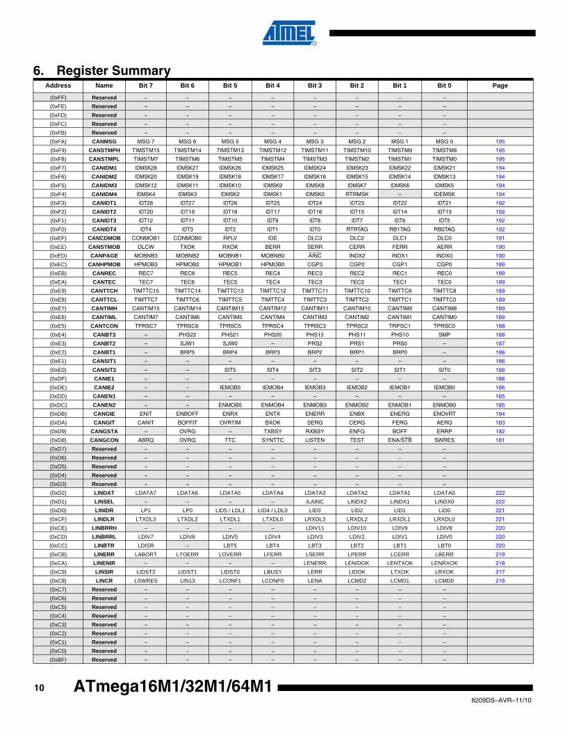
6. Register SummaryAddress Name Bit 7 Bit 6 Bit 5 Bit 4 Bit 3 Bit 2 Bit 1 Bit 0 Page
(0xFF) Reserved – – – – – – – –(0xFE) Reserved – – – – – – – –(0xFD) Reserved – – – – – – – –(0xFC) Reserved – – – – – – – –(0xFB) Reserved – – – – – – – –(0xFA) CANMSG MSG 7 MSG 6 MSG 5 MSG 4 MSG 3 MSG 2 MSG 1 MSG 0 195
(0xF9) CANSTMPH TIMSTM15 TIMSTM14 TIMSTM13 TIMSTM12 TIMSTM11 TIMSTM10 TIMSTM9 TIMSTM8 195
(0xF8) CANSTMPL TIMSTM7 TIMSTM6 TIMSTM5 TIMSTM4 TIMSTM3 TIMSTM2 TIMSTM1 TIMSTM0 195
(0xF7) CANIDM1 IDMSK28 IDMSK27 IDMSK26 IDMSK25 IDMSK24 IDMSK23 IDMSK22 IDMSK21 194
(0xF6) CANIDM2 IDMSK20 IDMSK19 IDMSK18 IDMSK17 IDMSK16 IDMSK15 IDMSK14 IDMSK13 194
(0xF5) CANIDM3 IDMSK12 IDMSK11 IDMSK10 IDMSK9 IDMSK8 IDMSK7 IDMSK6 IDMSK5 194
(0xF4) CANIDM4 IDMSK4 IDMSK3 IDMSK2 IDMSK1 IDMSK0 RTRMSK – IDEMSK 194
(0xF3) CANIDT1 IDT28 IDT27 IDT26 IDT25 IDT24 IDT23 IDT22 IDT21 192
(0xF2) CANIDT2 IDT20 IDT19 IDT18 IDT17 IDT16 IDT15 IDT14 IDT13 192
(0xF1) CANIDT3 IDT12 IDT11 IDT10 IDT9 IDT8 IDT7 IDT6 IDT5 192
(0xF0) CANIDT4 IDT4 IDT3 IDT2 IDT1 IDT0 RTRTAG RB1TAG RB0TAG 192
(0xEF) CANCDMOB CONMOB1 CONMOB0 RPLV IDE DLC3 DLC2 DLC1 DLC0 191
(0xEE) CANSTMOB DLCW TXOK RXOK BERR SERR CERR FERR AERR 190
(0xED) CANPAGE MOBNB3 MOBNB2 MOBNB1 MOBNB0 AINC INDX2 INDX1 INDX0 190
(0xEC) CANHPMOB HPMOB3 HPMOB2 HPMOB1 HPMOB0 CGP3 CGP2 CGP1 CGP0 189
(0xEB) CANREC REC7 REC6 REC5 REC4 REC3 REC2 REC1 REC0 189
(0xEA) CANTEC TEC7 TEC6 TEC5 TEC4 TEC3 TEC2 TEC1 TEC0 189
(0xE9) CANTTCH TIMTTC15 TIMTTC14 TIMTTC13 TIMTTC12 TIMTTC11 TIMTTC10 TIMTTC9 TIMTTC8 189
(0xE8) CANTTCL TIMTTC7 TIMTTC6 TIMTTC5 TIMTTC4 TIMTTC3 TIMTTC2 TIMTTC1 TIMTTC0 189
(0xE7) CANTIMH CANTIM15 CANTIM14 CANTIM13 CANTIM12 CANTIM11 CANTIM10 CANTIM9 CANTIM8 189
(0xE6) CANTIML CANTIM7 CANTIM6 CANTIM5 CANTIM4 CANTIM3 CANTIM2 CANTIM1 CANTIM0 189
(0xE5) CANTCON TPRSC7 TPRSC6 TPRSC5 TPRSC4 TPRSC3 TPRSC2 TRPSC1 TPRSC0 188
(0xE4) CANBT3 – PHS22 PHS21 PHS20 PHS12 PHS11 PHS10 SMP 188
(0xE3) CANBT2 – SJW1 SJW0 – PRS2 PRS1 PRS0 – 187
(0xE2) CANBT1 – BRP5 BRP4 BRP3 BRP2 BRP1 BRP0 – 186
(0xE1) CANSIT1 – – – – – – – – 186
(0xE0) CANSIT2 – – SIT5 SIT4 SIT3 SIT2 SIT1 SIT0 186
(0xDF) CANIE1 – – – – – – – – 186
(0xDE) CANIE2 – – IEMOB5 IEMOB4 IEMOB3 IEMOB2 IEMOB1 IEMOB0 186
(0xDD) CANEN1 – – – – – – – – 185
(0xDC) CANEN2 – – ENMOB5 ENMOB4 ENMOB3 ENMOB2 ENMOB1 ENMOB0 185
(0xDB) CANGIE ENIT ENBOFF ENRX ENTX ENERR ENBX ENERG ENOVRT 184
(0xDA) CANGIT CANIT BOFFIT OVRTIM BXOK SERG CERG FERG AERG 183
(0xD9) CANGSTA – OVRG – TXBSY RXBSY ENFG BOFF ERRP 182
(0xD8) CANGCON ABRQ OVRQ TTC SYNTTC LISTEN TEST ENA/STB SWRES 181
(0xD7) Reserved – – – – – – – –(0xD6) Reserved – – – – – – – –(0xD5) Reserved – – – – – – – –(0xD4) Reserved – – – – – – – –(0xD3) Reserved – – – – – – – –(0xD2) LINDAT LDATA7 LDATA6 LDATA5 LDATA4 LDATA3 LDATA2 LDATA1 LDATA0 222
(0xD1) LINSEL – – – – /LAINC LINDX2 LINDX1 LINDX0 222
(0xD0) LINIDR LP1 LP0 LID5 / LDL1 LID4 / LDL0 LID3 LID2 LID1 LID0 221
(0xCF) LINDLR LTXDL3 LTXDL2 LTXDL1 LTXDL0 LRXDL3 LRXDL2 LRXDL1 LRXDL0 221
(0xCE) LINBRRH – – – – LDIV11 LDIV10 LDIV9 LDIV8 220
(0xCD) LINBRRL LDIV7 LDIV6 LDIV5 LDIV4 LDIV3 LDIV2 LDIV1 LDIV0 220
(0xCC) LINBTR LDISR – LBT5 LBT4 LBT3 LBT2 LBT1 LBT0 220
(0xCB) LINERR LABORT LTOERR LOVERR LFERR LSERR LPERR LCERR LBERR 219
(0xCA) LINENIR – – – – LENERR LENIDOK LENTXOK LENRXOK 218
(0xC9) LINSIR LIDST2 LIDST1 LIDST0 LBUSY LERR LIDOK LTXOK LRXOK 217
(0xC8) LINCR LSWRES LIN13 LCONF1 LCONF0 LENA LCMD2 LCMD1 LCMD0 216
(0xC7) Reserved – – – – – – – –(0xC6) Reserved – – – – – – – –(0xC5) Reserved – – – – – – – –(0xC4) Reserved – – – – – – – –(0xC3) Reserved – – – – – – – –(0xC2) Reserved – – – – – – – –(0xC1) Reserved – – – – – – – –(0xC0) Reserved – – – – – – – –(0xBF) Reserved – – – – – – – –
118209DS–AVR–11/10
ATmega16M1/32M1/64M1
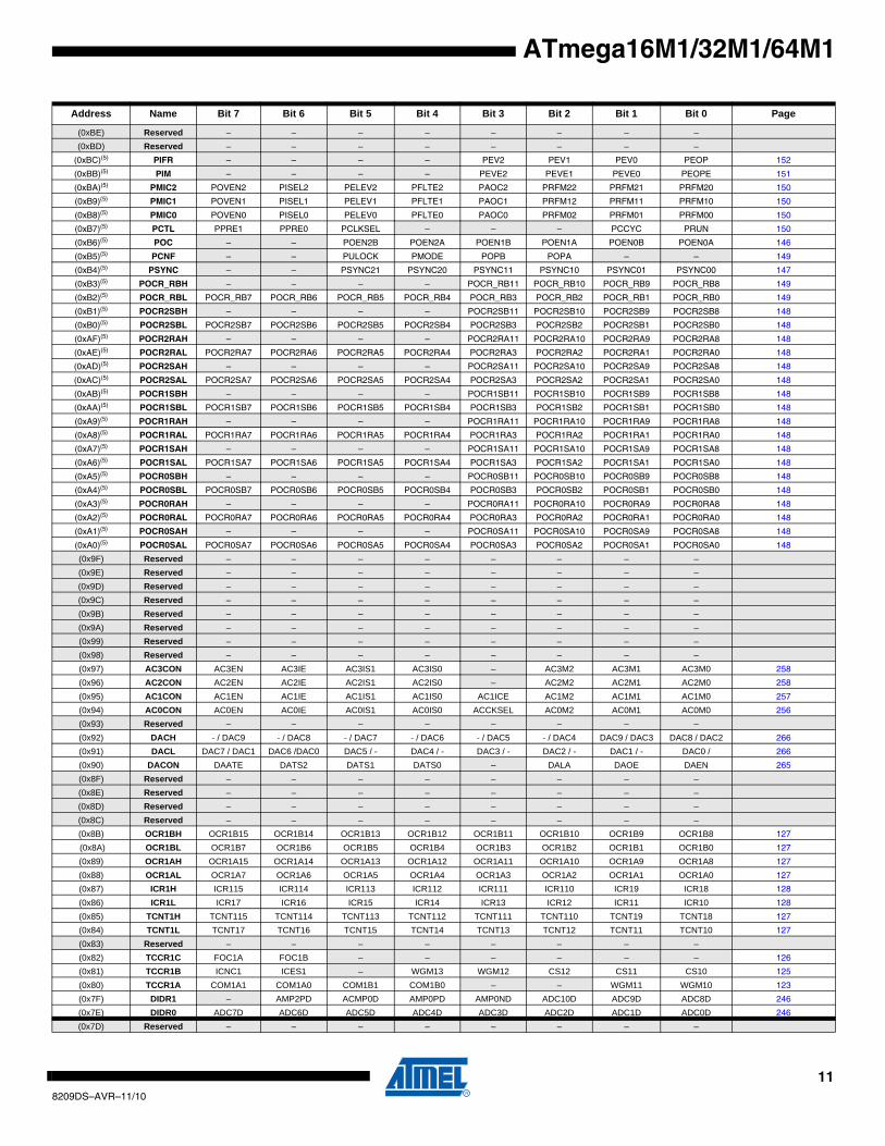
(0xBE) Reserved – – – – – – – –(0xBD) Reserved – – – – – – – –
(0xBC)(5) PIFR – – – – PEV2 PEV1 PEV0 PEOP 152
(0xBB)(5) PIM – – – – PEVE2 PEVE1 PEVE0 PEOPE 151
(0xBA)(5) PMIC2 POVEN2 PISEL2 PELEV2 PFLTE2 PAOC2 PRFM22 PRFM21 PRFM20 150
(0xB9)(5) PMIC1 POVEN1 PISEL1 PELEV1 PFLTE1 PAOC1 PRFM12 PRFM11 PRFM10 150
(0xB8)(5) PMIC0 POVEN0 PISEL0 PELEV0 PFLTE0 PAOC0 PRFM02 PRFM01 PRFM00 150
(0xB7)(5) PCTL PPRE1 PPRE0 PCLKSEL – – – PCCYC PRUN 150
(0xB6)(5) POC – – POEN2B POEN2A POEN1B POEN1A POEN0B POEN0A 146
(0xB5)(5) PCNF – – PULOCK PMODE POPB POPA – – 149
(0xB4)(5) PSYNC – – PSYNC21 PSYNC20 PSYNC11 PSYNC10 PSYNC01 PSYNC00 147
(0xB3)(5) POCR_RBH – – – – POCR_RB11 POCR_RB10 POCR_RB9 POCR_RB8 149
(0xB2)(5) POCR_RBL POCR_RB7 POCR_RB6 POCR_RB5 POCR_RB4 POCR_RB3 POCR_RB2 POCR_RB1 POCR_RB0 149
(0xB1)(5) POCR2SBH – – – – POCR2SB11 POCR2SB10 POCR2SB9 POCR2SB8 148
(0xB0)(5) POCR2SBL POCR2SB7 POCR2SB6 POCR2SB5 POCR2SB4 POCR2SB3 POCR2SB2 POCR2SB1 POCR2SB0 148
(0xAF)(5) POCR2RAH – – – – POCR2RA11 POCR2RA10 POCR2RA9 POCR2RA8 148
(0xAE)(5) POCR2RAL POCR2RA7 POCR2RA6 POCR2RA5 POCR2RA4 POCR2RA3 POCR2RA2 POCR2RA1 POCR2RA0 148
(0xAD)(5) POCR2SAH – – – – POCR2SA11 POCR2SA10 POCR2SA9 POCR2SA8 148
(0xAC)(5) POCR2SAL POCR2SA7 POCR2SA6 POCR2SA5 POCR2SA4 POCR2SA3 POCR2SA2 POCR2SA1 POCR2SA0 148
(0xAB)(5) POCR1SBH – – – – POCR1SB11 POCR1SB10 POCR1SB9 POCR1SB8 148
(0xAA)(5) POCR1SBL POCR1SB7 POCR1SB6 POCR1SB5 POCR1SB4 POCR1SB3 POCR1SB2 POCR1SB1 POCR1SB0 148
(0xA9)(5) POCR1RAH – – – – POCR1RA11 POCR1RA10 POCR1RA9 POCR1RA8 148
(0xA8)(5) POCR1RAL POCR1RA7 POCR1RA6 POCR1RA5 POCR1RA4 POCR1RA3 POCR1RA2 POCR1RA1 POCR1RA0 148
(0xA7)(5) POCR1SAH – – – – POCR1SA11 POCR1SA10 POCR1SA9 POCR1SA8 148
(0xA6)(5) POCR1SAL POCR1SA7 POCR1SA6 POCR1SA5 POCR1SA4 POCR1SA3 POCR1SA2 POCR1SA1 POCR1SA0 148
(0xA5)(5) POCR0SBH – – – – POCR0SB11 POCR0SB10 POCR0SB9 POCR0SB8 148
(0xA4)(5) POCR0SBL POCR0SB7 POCR0SB6 POCR0SB5 POCR0SB4 POCR0SB3 POCR0SB2 POCR0SB1 POCR0SB0 148
(0xA3)(5) POCR0RAH – – – – POCR0RA11 POCR0RA10 POCR0RA9 POCR0RA8 148
(0xA2)(5) POCR0RAL POCR0RA7 POCR0RA6 POCR0RA5 POCR0RA4 POCR0RA3 POCR0RA2 POCR0RA1 POCR0RA0 148
(0xA1)(5) POCR0SAH – – – – POCR0SA11 POCR0SA10 POCR0SA9 POCR0SA8 148
(0xA0)(5) POCR0SAL POCR0SA7 POCR0SA6 POCR0SA5 POCR0SA4 POCR0SA3 POCR0SA2 POCR0SA1 POCR0SA0 148
(0x9F) Reserved – – – – – – – –(0x9E) Reserved – – – – – – – –(0x9D) Reserved – – – – – – – –(0x9C) Reserved – – – – – – – –(0x9B) Reserved – – – – – – – –(0x9A) Reserved – – – – – – – –(0x99) Reserved – – – – – – – –(0x98) Reserved – – – – – – – –(0x97) AC3CON AC3EN AC3IE AC3IS1 AC3IS0 – AC3M2 AC3M1 AC3M0 258
(0x96) AC2CON AC2EN AC2IE AC2IS1 AC2IS0 – AC2M2 AC2M1 AC2M0 258
(0x95) AC1CON AC1EN AC1IE AC1IS1 AC1IS0 AC1ICE AC1M2 AC1M1 AC1M0 257
(0x94) AC0CON AC0EN AC0IE AC0IS1 AC0IS0 ACCKSEL AC0M2 AC0M1 AC0M0 256
(0x93) Reserved – – – – – – – –(0x92) DACH - / DAC9 - / DAC8 - / DAC7 - / DAC6 - / DAC5 - / DAC4 DAC9 / DAC3 DAC8 / DAC2 266
(0x91) DACL DAC7 / DAC1 DAC6 /DAC0 DAC5 / - DAC4 / - DAC3 / - DAC2 / - DAC1 / - DAC0 / 266
(0x90) DACON DAATE DATS2 DATS1 DATS0 – DALA DAOE DAEN 265
(0x8F) Reserved – – – – – – – –(0x8E) Reserved – – – – – – – –(0x8D) Reserved – – – – – – – –(0x8C) Reserved – – – – – – – –(0x8B) OCR1BH OCR1B15 OCR1B14 OCR1B13 OCR1B12 OCR1B11 OCR1B10 OCR1B9 OCR1B8 127
(0x8A) OCR1BL OCR1B7 OCR1B6 OCR1B5 OCR1B4 OCR1B3 OCR1B2 OCR1B1 OCR1B0 127
(0x89) OCR1AH OCR1A15 OCR1A14 OCR1A13 OCR1A12 OCR1A11 OCR1A10 OCR1A9 OCR1A8 127
(0x88) OCR1AL OCR1A7 OCR1A6 OCR1A5 OCR1A4 OCR1A3 OCR1A2 OCR1A1 OCR1A0 127
(0x87) ICR1H ICR115 ICR114 ICR113 ICR112 ICR111 ICR110 ICR19 ICR18 128
(0x86) ICR1L ICR17 ICR16 ICR15 ICR14 ICR13 ICR12 ICR11 ICR10 128
(0x85) TCNT1H TCNT115 TCNT114 TCNT113 TCNT112 TCNT111 TCNT110 TCNT19 TCNT18 127
(0x84) TCNT1L TCNT17 TCNT16 TCNT15 TCNT14 TCNT13 TCNT12 TCNT11 TCNT10 127
(0x83) Reserved – – – – – – – –(0x82) TCCR1C FOC1A FOC1B – – – – – – 126
(0x81) TCCR1B ICNC1 ICES1 – WGM13 WGM12 CS12 CS11 CS10 125
(0x80) TCCR1A COM1A1 COM1A0 COM1B1 COM1B0 – – WGM11 WGM10 123
(0x7F) DIDR1 – AMP2PD ACMP0D AMP0PD AMP0ND ADC10D ADC9D ADC8D 246
(0x7E) DIDR0 ADC7D ADC6D ADC5D ADC4D ADC3D ADC2D ADC1D ADC0D 246
(0x7D) Reserved – – – – – – – –
Address Name Bit 7 Bit 6 Bit 5 Bit 4 Bit 3 Bit 2 Bit 1 Bit 0 Page
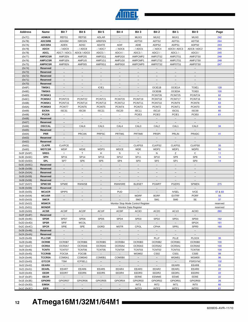
128209DS–AVR–11/10
ATmega16M1/32M1/64M1
(0x7C) ADMUX REFS1 REFS0 ADLAR – MUX3 MUX2 MUX1 MUX0 242
(0x7B) ADCSRB ADHSM ISRCEN AREFEN – ADTS3 ADTS2 ADTS1 ADTS0 244
(0x7A) ADCSRA ADEN ADSC ADATE ADIF ADIE ADPS2 ADPS1 ADPS0 243
(0x79) ADCH - / ADC9 - / ADC8 - / ADC7 - / ADC6 - / ADC5 - / ADC4 ADC9 / ADC3 ADC8 / ADC2 245
(0x78) ADCL ADC7 / ADC1 ADC6 / ADC0 ADC5 / - ADC4 / - ADC3 / - ADC2 / - ADC1 / - ADC0 / 245
(0x77) AMP2CSR AMP2EN AMP2IS AMP2G1 AMP2G0 AMPCMP2 AMP2TS2 AMP2TS1 AMP2TS0 248
(0x76) AMP1CSR AMP1EN AMP1IS AMP1G1 AMP1G0 AMPCMP1 AMP1TS2 AMP1TS1 AMP1TS0 248
(0x75) AMP0CSR AMP0EN AMP0IS AMP0G1 AMP0G0 AMPCMP0 AMP0TS2 AMP0TS1 AMP0TS0 247
(0x74) Reserved – – – – – – – –(0x73) Reserved – – – – – – – –(0x72) Reserved – – – – – – – –(0x71) Reserved – – – – – – – –(0x70) Reserved – – – – – – – –(0x6F) TIMSK1 – – ICIE1 – – OCIE1B OCIE1A TOIE1 128
(0x6E) TIMSK0 – – – – – OCIE0B OCIE0A TOIE0 100
(0x6D) PCMSK3 – – – – – PCINT26 PCINT25 PCINT24 62
(0x6C) PCMSK2 PCINT23 PCINT22 PCINT21 PCINT20 PCINT19 PCINT18 PCINT17 PCINT16 63
(0x6B) PCMSK1 PCINT15 PCINT14 PCINT13 PCINT12 PCINT11 PCINT10 PCINT9 PCINT8 63
(0x6A) PCMSK0 PCINT7 PCINT6 PCINT5 PCINT4 PCINT3 PCINT2 PCINT1 PCINT0 63
(0x69) EICRA ISC31 ISC30 ISC21 ISC20 ISC11 ISC10 ISC01 ISC00 60
(0x68) PCICR – – – – PCIE3 PCIE2 PCIE1 PCIE0 61
(0x68) Reserved – – – – – – – –(0x67) Reserved – – – – – – – –(0x66) OSCCAL – CAL6 CAL5 CAL4 CAL3 CAL2 CAL1 CAL0 34
(0x65) Reserved – – – – – – – –(0x64) PRR – PRCAN PRPSC PRTIM1 PRTIM0 PRSPI PRLIN PRADC 41
(0x63) Reserved – – – – – – – –(0x62) Reserved – – – – – – – –(0x61) CLKPR CLKPCE – – – CLKPS3 CLKPS2 CLKPS1 CLKPS0 35
(0x60) WDTCSR WDIF WDIE WDP3 WDCE WDE WDP2 WDP1 WDP0 50
0x3F (0x5F) SREG I T H S V N Z C 11
0x3E (0x5E) SPH SP15 SP14 SP13 SP12 SP11 SP10 SP9 SP8 14
0x3D (0x5D) SPL SP7 SP6 SP5 SP4 SP3 SP2 SP1 SP0 14
0x3C (0x5C) Reserved – – – – – – – –0x3B (0x5B) Reserved – – – – – – – –0x3A (0x5A) Reserved – – – – – – – –0x39 (0x59) Reserved – – – – – – – –0x38 (0x58) Reserved – – – – – – – –0x37 (0x57) SPMCSR SPMIE RWWSB – RWWSRE BLBSET PGWRT PGERS SPMEN 275
0x36 (0x56) Reserved – – – – – – – –0x35 (0x55) MCUCR SPIPS – – PUD – – IVSEL IVCE 57 & 83
0x34 (0x54) MCUSR – – – – WDRF BORF EXTRF PORF 50
0x33 (0x53) SMCR – – – – SM2 SM1 SM0 SE 37
0x32 (0x52) MSMCR Monitor Stop Mode Control Register reserved0x31 (0x51) MONDR Monitor Data Register reserved0x30 (0x50) ACSR AC3IF AC2IF AC1IF AC0IF AC3O AC2O AC1O AC0O 260
0x2F (0x4F) Reserved – – – – – – – –0x2E (0x4E) SPDR SPD7 SPD6 SPD5 SPD4 SPD3 SPD2 SPD1 SPD0 162
0x2D (0x4D) SPSR SPIF WCOL – – – – – SPI2X 161
0x2C (0x4C) SPCR SPIE SPE DORD MSTR CPOL CPHA SPR1 SPR0 160
0x2B (0x4B) Reserved – – – – – – – –0x2A (0x4A) Reserved – – – – – – – –0x29 (0x49) PLLCSR - - - - - PLLF PLLE PLOCK 35
0x28 (0x48) OCR0B OCR0B7 OCR0B6 OCR0B5 OCR0B4 OCR0B3 OCR0B2 OCR0B1 OCR0B0 100
0x27 (0x47) OCR0A OCR0A7 OCR0A6 OCR0A5 OCR0A4 OCR0A3 OCR0A2 OCR0A1 OCR0A0 100
0x26 (0x46) TCNT0 TCNT07 TCNT06 TCNT05 TCNT04 TCNT03 TCNT02 TCNT01 TCNT00 100
0x25 (0x45) TCCR0B FOC0A FOC0B – – WGM02 CS02 CS01 CS00 99
0x24 (0x44) TCCR0A COM0A1 COM0A0 COM0B1 COM0B0 – – WGM01 WGM00 96
0x23 (0x43) GTCCR TSM ICPSEL1 – – – – – PSRSYNC 132
0x22 (0x42) EEARH – – – – – – EEAR9 EEAR8 22
0x21 (0x41) EEARL EEAR7 EEAR6 EEAR5 EEAR4 EEAR3 EEAR2 EEAR1 EEAR0 22
0x20 (0x40) EEDR EEDR7 EEDR6 EEDR5 EEDR4 EEDR3 EEDR2 EEDR1 EEDR0 22
0x1F (0x3F) EECR – – – – EERIE EEMWE EEWE EERE 22
0x1E (0x3E) GPIOR0 GPIOR07 GPIOR06 GPIOR05 GPIOR04 GPIOR03 GPIOR02 GPIOR01 GPIOR00 26
0x1D (0x3D) EIMSK – – – – INT3 INT2 INT1 INT0 60
0x1C (0x3C) EIFR – – – – INTF3 INTF2 INTF1 INTF0 61
Address Name Bit 7 Bit 6 Bit 5 Bit 4 Bit 3 Bit 2 Bit 1 Bit 0 Page
138209DS–AVR–11/10
ATmega16M1/32M1/64M1
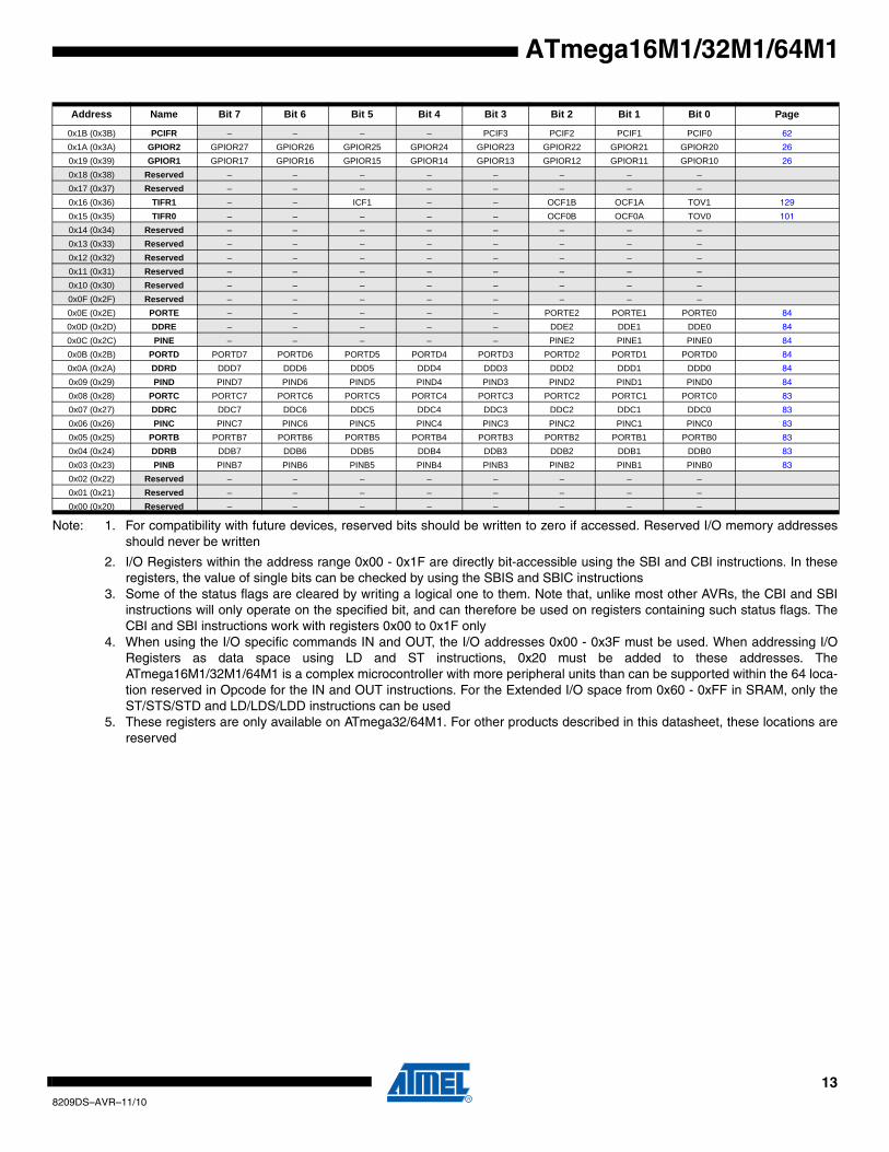
Note: 1. For compatibility with future devices, reserved bits should be written to zero if accessed. Reserved I/O memory addressesshould never be written
2. I/O Registers within the address range 0x00 - 0x1F are directly bit-accessible using the SBI and CBI instructions. In theseregisters, the value of single bits can be checked by using the SBIS and SBIC instructions
3. Some of the status flags are cleared by writing a logical one to them. Note that, unlike most other AVRs, the CBI and SBIinstructions will only operate on the specified bit, and can therefore be used on registers containing such status flags. TheCBI and SBI instructions work with registers 0x00 to 0x1F only
4. When using the I/O specific commands IN and OUT, the I/O addresses 0x00 - 0x3F must be used. When addressing I/ORegisters as data space using LD and ST instructions, 0x20 must be added to these addresses. TheATmega16M1/32M1/64M1 is a complex microcontroller with more peripheral units than can be supported within the 64 loca-tion reserved in Opcode for the IN and OUT instructions. For the Extended I/O space from 0x60 - 0xFF in SRAM, only theST/STS/STD and LD/LDS/LDD instructions can be used
5. These registers are only available on ATmega32/64M1. For other products described in this datasheet, these locations arereserved
0x1B (0x3B) PCIFR – – – – PCIF3 PCIF2 PCIF1 PCIF0 62
0x1A (0x3A) GPIOR2 GPIOR27 GPIOR26 GPIOR25 GPIOR24 GPIOR23 GPIOR22 GPIOR21 GPIOR20 26
0x19 (0x39) GPIOR1 GPIOR17 GPIOR16 GPIOR15 GPIOR14 GPIOR13 GPIOR12 GPIOR11 GPIOR10 26
0x18 (0x38) Reserved – – – – – – – –0x17 (0x37) Reserved – – – – – – – –0x16 (0x36) TIFR1 – – ICF1 – – OCF1B OCF1A TOV1 129
0x15 (0x35) TIFR0 – – – – – OCF0B OCF0A TOV0 101
0x14 (0x34) Reserved – – – – – – – –0x13 (0x33) Reserved – – – – – – – –0x12 (0x32) Reserved – – – – – – – –0x11 (0x31) Reserved – – – – – – – –0x10 (0x30) Reserved – – – – – – – –0x0F (0x2F) Reserved – – – – – – – –0x0E (0x2E) PORTE – – – – – PORTE2 PORTE1 PORTE0 84
0x0D (0x2D) DDRE – – – – – DDE2 DDE1 DDE0 84
0x0C (0x2C) PINE – – – – – PINE2 PINE1 PINE0 84
0x0B (0x2B) PORTD PORTD7 PORTD6 PORTD5 PORTD4 PORTD3 PORTD2 PORTD1 PORTD0 84
0x0A (0x2A) DDRD DDD7 DDD6 DDD5 DDD4 DDD3 DDD2 DDD1 DDD0 84
0x09 (0x29) PIND PIND7 PIND6 PIND5 PIND4 PIND3 PIND2 PIND1 PIND0 84
0x08 (0x28) PORTC PORTC7 PORTC6 PORTC5 PORTC4 PORTC3 PORTC2 PORTC1 PORTC0 83
0x07 (0x27) DDRC DDC7 DDC6 DDC5 DDC4 DDC3 DDC2 DDC1 DDC0 83
0x06 (0x26) PINC PINC7 PINC6 PINC5 PINC4 PINC3 PINC2 PINC1 PINC0 83
0x05 (0x25) PORTB PORTB7 PORTB6 PORTB5 PORTB4 PORTB3 PORTB2 PORTB1 PORTB0 83
0x04 (0x24) DDRB DDB7 DDB6 DDB5 DDB4 DDB3 DDB2 DDB1 DDB0 83
0x03 (0x23) PINB PINB7 PINB6 PINB5 PINB4 PINB3 PINB2 PINB1 PINB0 83
0x02 (0x22) Reserved – – – – – – – –0x01 (0x21) Reserved – – – – – – – –0x00 (0x20) Reserved – – – – – – – –
Address Name Bit 7 Bit 6 Bit 5 Bit 4 Bit 3 Bit 2 Bit 1 Bit 0 Page

148209DS–AVR–11/10
ATmega16M1/32M1/64M1
7. Errata
7.1 Errata ATmega16M1The revision letter in this section refers to revisions of the ATmega16M1 device.
7.1.1 Rev. ANot sampled.
7.2 Errata ATmega32M1The revision letter in this section refers to revisions of the ATmega32M1 device.
7.2.1 Rev. ANot sampled.
7.3 Errata ATmega64M1The revision letter in this section refers to revisions of the ATmega64M1 device.
7.3.1 Rev. ANot sampled.

158209DS–AVR–11/10
ATmega16M1/32M1/64M1
8. Ordering Information
8.1 ATmega16M1
Note: All packages are Pb free, fully LHF
Speed Power Supply Ordering Code Package Operation Range
16MHz 2.7V - 5.5VATmega16M1 - AU 32A Industrial
(-40°C to 85°C)ATmega16M1 - MU PV
Package Type
32A 32-lead, Thin (1.0mm) Plastic Quad Flat Package (TQFP)
PV PV, 32-Lead, 7.0mm × 7.0mm Body, 0.65mm Pitch Quad Flat No Lead Package (QFN)
168209DS–AVR–11/10
ATmega16M1/32M1/64M1
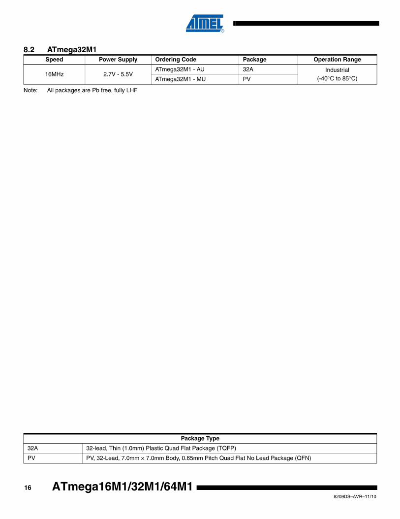
8.2 ATmega32M1
Note: All packages are Pb free, fully LHF
Speed Power Supply Ordering Code Package Operation Range
16MHz 2.7V - 5.5VATmega32M1 - AU 32A Industrial
(-40°C to 85°C)ATmega32M1 - MU PV
Package Type
32A 32-lead, Thin (1.0mm) Plastic Quad Flat Package (TQFP)
PV PV, 32-Lead, 7.0mm × 7.0mm Body, 0.65mm Pitch Quad Flat No Lead Package (QFN)

178209DS–AVR–11/10
ATmega16M1/32M1/64M1
8.3 ATmega64M1
Note: All packages are Pb free, fully LHF
Speed Power Supply Ordering Code Package Operation Range
16MHz 2.7V - 5.5VATmega64M1 - AU 32A Industrial
(-40°C to 85°C)ATmega64M1 - MU PV
Package Type
32A 32-lead, Thin (1.0mm) Plastic Quad Flat Package (TQFP)
PV PV, 32-Lead, 7.0mm × 7.0mm Body, 0.65mm Pitch Quad Flat No Lead Package (QFN)
188209DS–AVR–11/10
ATmega16M1/32M1/64M1
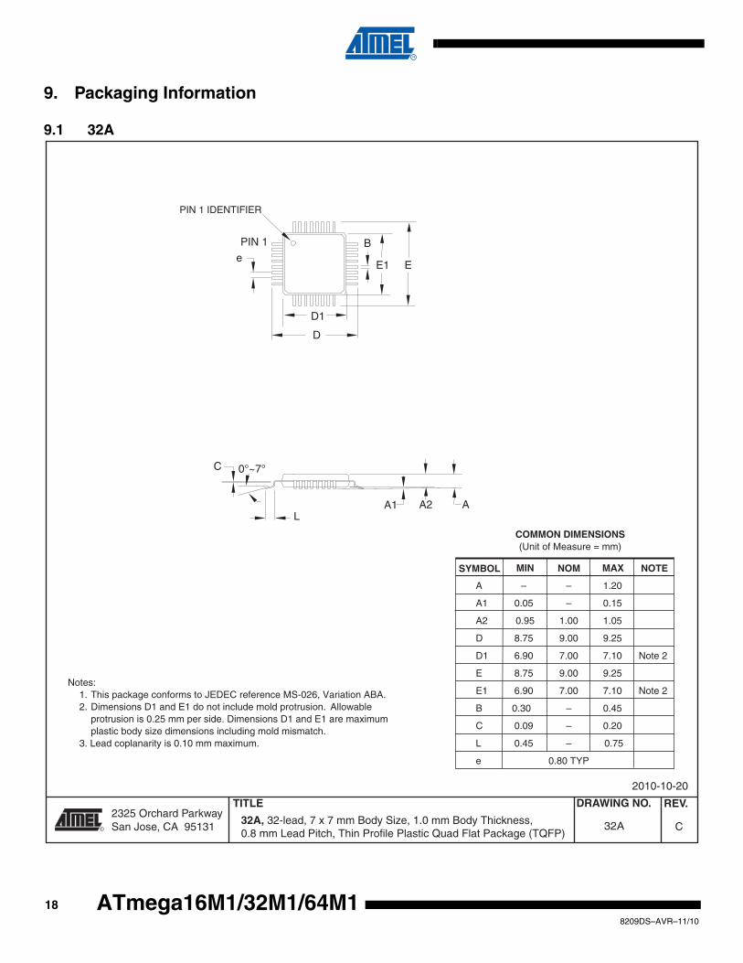
9. Packaging Information
9.1 32A
2325 Orchard Parkway San Jose, CA 95131
TITLE DRAWING NO.
R
REV.
32A, 32-lead, 7 x 7 mm Body Size, 1.0 mm Body Thickness,0.8 mm Lead Pitch, Thin Profile Plastic Quad Flat Package (TQFP)
C32A
2010-10-20
PIN 1 IDENTIFIER
0°~7°
PIN 1
L
C
A1 A2 A
D1
D
eE1 E
B
Notes: 1. This package conforms to JEDEC reference MS-026, Variation ABA. 2. Dimensions D1 and E1 do not include mold protrusion. Allowable protrusion is 0.25 mm per side. Dimensions D1 and E1 are maximum plastic body size dimensions including mold mismatch. 3. Lead coplanarity is 0.10 mm maximum.
A – – 1.20
A1 0.05 – 0.15
A2 0.95 1.00 1.05
D 8.75 9.00 9.25
D1 6.90 7.00 7.10 Note 2
E 8.75 9.00 9.25
E1 6.90 7.00 7.10 Note 2
B 0.30 – 0.45
C 0.09 – 0.20
L 0.45 – 0.75
e 0.80 TYP
COMMON DIMENSIONS(Unit of Measure = mm)
SYMBOL MIN NOM MAX NOTE
198209DS–AVR–11/10
ATmega16M1/32M1/64M1
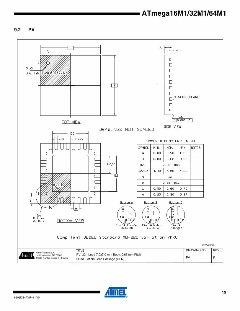
9.2 PV

208209DS–AVR–11/10
ATmega16M1/32M1/64M1
10. Datasheet Revision HistoryPlease note that the referring page numbers in this section are referred to this document. Thereferring revision in this section are referring to the document revision.
10.1 8209D – 11/10
10.2 8209C – 05/10
10.3 8209B – 10/09
10.4 8209A – 08/09
1. Updated footnote 1in “Features” on page 1.
2. Removed the chapter “Disclaimer” from the datasheet.
3. Updated the table Table 27-18 on page 305 with a correct reference for Read Fuse bits.
4. Updated “SPI Serial Programming Characteristics” on page 306 with correct link.
5.Added typical values for for RAIN and CAIN (both “single ended input” and “differential inputs”) in Table 28-7 on page 314.
6. Added “PCICR” in “Register Summary” on page 320.
7. Editing updates
8. Updated the last page according to Atmel new Brand Style Guide.
1. Replaced 32M1-A package information drawing with PV drawing on page 334.
2. Updated ordering information with correct info on PV package.
1. Updated “Temperature Measurement” on page 236.
2. Updated “Manufacturing Calibration” on page 237.
1. Initial revision.
i8209DS–AVR–11/10
ATmega16M1/32M1/64M1
Table of Contents
Features ..................................................................................................... 1
1 Pin Configurations ................................................................................... 2
1.1 Pin Descriptions .................................................................................................3
2 Overview ................................................................................................... 5
2.1 Block Diagram ...................................................................................................6
2.2 Pin Descriptions .................................................................................................7
3 Resources ................................................................................................. 9
4 About Code Examples ............................................................................. 9
5 Data Retention .......................................................................................... 9
6 Register Summary ................................................................................. 10
7 Errata ....................................................................................................... 14
7.1 Errata ATmega16M1 .......................................................................................14
7.2 Errata ATmega32M1 .......................................................................................14
7.3 Errata ATmega64M1 .......................................................................................14
8 Ordering Information ............................................................................. 15
8.1 ATmega16M1 ..................................................................................................15
8.2 ATmega32M1 ..................................................................................................16
8.3 ATmega64M1 ..................................................................................................17
9 Packaging Information .......................................................................... 18
9.1 32A ..................................................................................................................18
9.2 PV ....................................................................................................................19
10 Datasheet Revision History .................................................................. 20
10.1 8209D – 11/10 .................................................................................................20
10.2 8209C – 05/10 .................................................................................................20
10.3 8209B – 10/09 .................................................................................................20
10.4 8209A – 08/09 .................................................................................................20
Table of Contents....................................................................................... i

8209DS–AVR–11/10
Atmel Corporation2325 Orchard ParkwaySan Jose, CA 95131USATel: (+1)(408) 441-0311Fax: (+1)(408) 487-2600 www.atmel.com
Atmel Asia LimitedUnit 1-5 & 16, 19/FBEA Tower, Millennium City 5418 Kwun Tong RoadKwun Tong, KowloonHONG KONGTel: (+852) 2245-6100Fax: (+852) 2722-1369
Atmel Munich GmbHBusiness CampusParkring 4D-85748 Garching b. MunichGERMANYTel: (+49) 89-31970-0Fax: (+49) 89-3194621
Atmel Japan9F, Tonetsu Shinkawa Bldg.1-24-8 ShinkawaChuo-ku, Tokyo 104-0033JAPANTel: (+81)(3) 3523-3551Fax: (+81)(3) 3523-7581
© 2010 Atmel Corporation. All rights reserved. / Rev. CORP072610
Atmel®, logo and combinations thereof, and others are registered trademarks or trademarks of Atmel Corporation or its subsidiaries. Other terms and product names may be trademarks of others.
Disclaimer: The information in this document is provided in connection with Atmel products. No license, express or implied, by estoppel or otherwise, to any intellectual property right is granted by this document or in connection with the sale of Atmel products. EXCEPT AS SET FORTH IN THE ATMEL TERMS AND CONDITIONS OF SALES LOCATED ON THE ATMEL WEBSITE, ATMEL ASSUMES NO LIABILITY WHATSOEVER AND DISCLAIMS ANY EXPRESS, IMPLIED OR STATUTORY WARRANTY RELATING TO ITS PRODUCTS INCLUDING, BUT NOT LIMITED TO, THE IMPLIED WARRANTY OF MERCHANTABILITY, FITNESS FOR A PARTICULAR PURPOSE, OR NON-INFRINGEMENT. IN NO EVENT SHALL ATMEL BE LIABLE FOR ANY DIRECT, INDIRECT, CONSEQUENTIAL, PUNITIVE, SPECIAL OR INCIDENTAL DAMAGES (INCLUDING, WITHOUT LIMITATION, DAMAGES FOR LOSS AND PROF-ITS, BUSINESS INTERRUPTION, OR LOSS OF INFORMATION) ARISING OUT OF THE USE OR INABILITY TO USE THIS DOCUMENT, EVEN IF ATMEL HAS BEEN ADVISED OF THE POSSIBILITY OF SUCH DAMAGES. Atmel makes no representations or warranties with respect to the accuracy or com-pleteness of the contents of this document and reserves the right to make changes to specifications and product descriptions at any time without notice. Atmel does not make any commitment to update the information contained herein. Unless specifically provided otherwise, Atmel products are not suit-able for, and shall not be used in, automotive applications. Atmel products are not intended, authorized, or warranted for use as components in applica-tions intended to support or sustain life.