Embed Size (px)
Citation preview

Image
Topic:
o Nam elementum commodo mattis. Pellentesque
malesuada blandit euismod.
Topic:
o Nam elementum commodo mattis. Pellentesque
malesuada blandit euismod.
o Nam elementum commodo mattis. Pellentesque
malesuada blandit euismod.
Topic:
o Nam elementum commodo mattis. Pellentesque
malesuada blandit euismod.
TITLE Enabling World’s first over 4.4Gbps/pin
at sub-1V LPDDR4 Interface using
Bandwidth Improvement Techniques
Billy(Kyoung-Hoi) Koo,
Jinho Choi, Kwanyeob Chae (Samsung)

Previous DesignCon

Technical Trend
Valid Window Margin(VWM)
Proposed LPDDR4 Interface:
o Low CIO Multi-VOH level Driver and Receiver
o Duty Adjustment Scheme
o Asymmetric Rise/Fall time Control Scheme
o On-die De-cap. Estimation
o Clean Data Strobe(DQS) Signal
DQS Cleaning Method
Test Results
o Valid Window Margin(VWM)
Conclusion
Outline

Memory Interface Speed Trend Future AP must have GPU performance to run high spec. PC games
Double the bandwidth every other year
B/W [GB/s]
Download Counts
51.2
25.6
12.8
100M+
Fill Rate [Gpixel/s]
2.5 5 10
Life Sim.
Adventure
Strategic
50M+
100M+

Design Challenges
Purpose of DDRPHY
Maximize the valid window margin under P/V/T variations,
thereby providing reliable memory access
PHY makes DQS edge is centered at DQ window at memory
or PHY
If not, the probability of bit-flip error increases
AP
Memory
On-chip
- Logic speed ↑, Gate counts ↑
- IR drop↑, Dynamic Voltage Drop(DvD) ↑
- Clock path jitter ↑, duty distortion ↑
Off-chip
- PKG size ↓
- Cross talk ↑
Process
- Process uncertainty↑
Memory
- Timing parameter variation ↑
- Density ↑
Hard to meet timing requirement on controller side

What is Valid Window Margin(VWM)
DQS
DQ
Normal Abnormal
1UI
-offset +offset
Centered-DQ
S
VWMPerror Perror
offset 0
AP

WRITE Mode VWM
On-Chip Reference clock jitter (A1-A2) PLL jitter (A3) Clock network jitter (A3-A5) Clock network duty (A3-A5)
Off-Chip Off-Chip clock jitter (A5-B2) Off-Chip clock duty (A5-B2) Off-Chip eye open ((A51-1)-(B2-1))

READ Mode VWM
On-Chip Reference clock jitter (A1-A2) PLL jitter (A3) Clock network jitter (A3-A5) Clock network duty (A3-A5) Read path jitter (B5-C2), Read path duty (B5-C2)
Off-Chip Off-Chip clock jitter (A5-B2) Off-Chip clock duty (A5-B2) Off-Chip eye open (B3-B5)

Technical Trend
Valid Window Margin(VWM)
Proposed LPDDR4 Interface:
o Low CIO Multi-VOH level Driver and Receiver
o Duty Adjustment Scheme
o Asymmetric Rise/Fall time Control Scheme
o On-die De-cap. Estimation
o Clean Data Strobe(DQS) Signal
DQS Cleaning Method
Test Results
o Valid Window Margin(VWM)
Conclusion
Outline

LPDDR4 Signaling and Multi-VOH Driver
Pull-up NMOS
Pull-down NMOS
Pull-down NMOS
Pull-up PMOS
OperationRegion
Calibration Point
Pull-upNMOS
Pull-upPMOS
Current
Current
CMOS driver(LPDDR3)
LVSTL driver(LPDDR4)
Current
V
V
V0
0
0
Difference Between LPDDR3 and LPDDR4 Multi-VOH Driver
Pull-up control
Pull-downcontrol
VOH
Data

Low CIO Transceiver
Proposed Transceiver Block [Source: DesignCon2013]
Out
VREF
Y
In
Receiver (VDDQ)
In
Out
VREF
ESDY
Receiver (VDD)
Driver (VDDQ) Driver (VDDQ)

Duty Adjustment Scheme(1)
30.00
35.00
40.00
45.00
50.00
55.00
60.00
30 35 40 45 50 55 60
Me
asu
re D
uty
(%)
Simulation Duty (%)
DQS
DQ
The duty control block is located at the first stage of
I/O and it consists of two CMOS inverter group which
is composed by the different kinds of strength pull up
and down transistors.
Driver Duty Control Scheme Duty Ratio Range
IN IN_DELAYCTRL
pctrl
nctrl

Duty Adjustment Scheme(2)
Asymmetric pre-driver control scheme for
DQS(or CLK) PAD can be adjust rise/fall
time of PADP and PADN independently.
PADP
PADPPU control
PADPPD control
PADN
PADNPU control
PADNPD control
PADP
PU control
PADN
PD control
PADP
PADN
PADP-PADN
High Duration = Low Duration High Duration = Low Duration
PADP : strong PU / weak PDPADN : strong PU / weak PD
PADP : medium PU / medium PDPADN : medium PU / medium PD
PADP : strong PU / weak PDPADN : weak PU / strong PD
High Duration > Low Duration

It is very critical to achieve cost-effective
PDN design with optimized on-die power
delivery network including de-cap and
power/ground grids. Also to reduce SSO
noise in weak Power Delivery Network
(PDN) condition such as POP package
environment, On-die de-cap insertion is
considered, but adding on-die de-cap
increases the chip size as one of
negative sides.
On-Die De-Cap. Estimation
Eye
op
en
ing
size
[ps]
on-die de-cap. [pf/IO]
VDDQDATA
VDDQCLOCK
w/o De-cap.w/ De-cap.
w/o De-cap.w/ De-cap.

Technical Trend
Valid Window Margin(VWM)
Proposed LPDDR4 Interface:
o Low CIO Multi-VOH level Driver and Receiver
o Duty Adjustment Scheme
o Asymmetric Rise/Fall time Control Scheme
o On-die De-cap. Estimation
o Clean Data Strobe(DQS) Signal
DQS Cleaning Method
Test Results
o Valid Window Margin(VWM)
Conclusion
Outline

READ DQS Glitch
Y_DQS used for clock in read-FIFO
At idle state (DQSP=DQSN=0)
Glitch occurs on DQS receiver output (Y_DQS)
READ FAIL
VSSQ
Y_DQS
DQSN
DQSP
DQSPDQSN
Y_DQS
Glitch Glitch
0

READ DQS Measurement
READ DQS ringing w/o ODT
READ DQS post-amble glitch w/ ODT enable
66.7mV
143.3mV

Remove DQS Glitch
During READ operation,
glitch occurs on Y_DQS at idle state (DQSP=DQSN=0)
Initial gate training,
generate optimized gate pulse to filter out glitch
Gate
Y_Clean_DQS
DQSPDQSN
Y_DQS
0
Glitch Glitch

DQS2CK Variation in Mobile DDR Large DQS2CK variation in mobile DDR due to absence of DLL
CK
DQS
tDQSCK = 1/TCK
CK
DQS
Clock tree
VT variation
CK
DQS
tDQSCK = 1.5 ~ 3.5ns
Native DDR Mobile DDRCK
DQS
DLL
tDQSCK tDQSCK
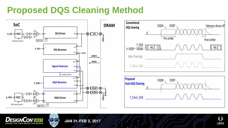
Proposed DQS Cleaning Method
DCC LS
Y_DQ
Inn
Inp
DQ ReceiverVREF
LSDCC
LS
Y
OutIn
OutIn
DQS Driver
A_DQ
A_DQS
Impp<2:0>Impn<2:0>
DQ duty control
DQS duty control
DQSP
DQSN
DQ
SoC DRAM
WRITE
READ
Y_DQS
OutIn DQ Driver
Impp<2:0>Impn<2:0>
Inn
vref
DQS Receiver
Signal Detector Inp
Inn
Inp
vref
mode control
DQSPDQSN
Post-amble
Memory driver off
0
Pre-amble
Y_DQS(= DQSP – DQSN)
Gate Training)
Y_Clean_DQS
Hi-Z Hi-Z
Conventional DQS cleaning
DQSPDQSN
0
Y_Clean_DQS
Proposed Auto-DQS Cleaning

Technical Trend
Valid Window Margin(VWM)
Proposed LPDDR4 Interface:
o Low CIO Multi-VOH level Driver and Receiver
o Duty Adjustment Scheme
o Asymmetric Rise/Fall time Control Scheme
o On-die De-cap. Estimation
o Clean Data Strobe(DQS) Signal
DQS Cleaning Method
Test Results
o Valid Window Margin(VWM)
Conclusion
Outline

Test Environment
Test Board Test Chip

Test Results
WRITE VWM @4420Mbps WRITE VWM @4420Mbps
Memory RAED/WRITE operation over 4.4Gbps with sufficient timing margin

Test Results
Driving Strength Dependency
o PDDS : pull-up driving strength
o DDS : pull-down driving strength
o Good VWM size: PDDS7-DDS7,
PDDS7-DDS4, PDDS4-DDS7
o DDS setting should be deiced VWM and
power consumption

Test Results Pattern types affects VWM size and offset
Memtester pattern was used to measure VWM

Test Results
WRITE
Optimal test pattern size
o WRITE : 500KB
READ
Optimal test pattern size
o READ : 1MB

Test Results
READ WRITE
DBI function affects VWM size and power consumption

Conclusion
Introduce Valid Window Margin
Proposed performance improvement IO design technique
DQS Cleaning Method
Various VWM test results
[email protected] LPDDR4 interface using 10nm FinFET process

---
QUESTIONS?
Thank you!