Embed Size (px)
Citation preview
ASIC DESIGN OF RF ENERGY HARVESTER USING 0.13UM CMOS
TECHNOLOGY
A Thesis
presented to
the Faculty of California Polytechnic State University,
San Luis Obispo
In Partial Fulfillment
of the Requirements for the Degree
Master of Science in Electrical Engineering
by
Jainish Zaveri
August 2018

ii
© 2018
Jainish Kiran Zaveri
ALL RIGHTS RESERVED
iii
COMMITTEE MEMBERSHIP
TITLE: ASIC Design of RF Energy Harvester using
0.13um CMOS Technology
AUTHOR:
Jainish Zaveri
DATE SUBMITTED:
August 2018
COMMITTEE CHAIR:
Dr. Tina Smilkstein, Ph. D
Professor of Electrical Engineering
COMMITTEE MEMBER: Dr. Andrew Danowitz, Ph. D
Professor of Electrical Engineering
COMMITTEE MEMBER:
Dr. Dennis Derickson, Ph. D
Professor of Electrical Engineering
iv
ABSTRACT
ASIC Design of RF Energy Harvester using 0.13um CMOS Technology
Jainish Zaveri
Recent advances in wireless sensor nodes, data acquisition devices, wearable and implantable
medical devices [1] [2] [3] have paved way for low power (sub 50uW) devices. These devices generally use
small solid-state or thin film batteries for power supply which need replacement or need to be removed for
charging. RF energy harvesting technology can be used to charge these batteries without the need to remove
the battery from the device, thus providing a sustainable power supply. In other cases, a battery can become
unnecessary altogether. This enables us to deploy wireless network nodes in places where regular physical
access to the nodes is difficult or cumbersome.
This thesis proposes a design of an RF energy harvesting device able to charge commercially
available thin film or solid-state batteries. The energy harvesting amplifier circuit is designed in Global
Foundry 0.13um CMOS technology using Cadence integrated circuit design tools. This Application Specific
Integrated Circuit (ASIC) is intended to have as small a footprint as possible so that it can be easily integrated
with the above-mentioned devices. While a dedicated RF power source is a direct solution to provide
sustainable power to the harvesting circuit, harvesting ambient RF power from TV and UHF cellular
frequencies increases the possibilities of where the harvesting device can be placed. The biggest challenge
for RF energy harvesting technology is the availability of adequate amount of RF power. This thesis also
presents a survey of available RF power at various ultra-high frequencies in San Luis Obispo, CA. The idea
is to determine the frequency band which can provide maximum RF power for harvesting and design a
harvester for that frequency band.
v
TABLE OF CONTENTS Page
LIST OF TABLES………………………………………………………………………………….. vi
LIST OF FIGURES………………………………………………………………………………… vii
CHAPTER 1: INTRODUCTION…………………………………………………………………. 1
CHAPTER 2: LITERATURE SURVEY………………………………………………………… 4
2.1 Availability of RF energy………………………………………………………………….. 4
2.1.1 Study of ambient RF power survey…………………………………………………. 5
2.1.2 Manual RF power source…………………………………………………………….. 8
2.2 Block diagram of RF energy harvester…………………………………………………… 8
2.3 Amplifier circuit…………………………………………………………………………….. 9
2.4 Solid state battery…………………………………………………………………………… 15
2.5 Conclusion…………………………………………………………………………………... 17
CHAPTER 3: RF POWER SURVEY……………………………………………………………. 18
3.1 Study of cellular communication frequency bands………………………………………. 18
3.2 RF power survey across SLO, CA………………………………………………………… 20
3.3 Conclusion…………………………………………………………………………………... 23
CHAPTER 4: ANTENNA DESIGN……………………………………………………………… 24
4.1 Antenna geometry…………………………………………………………………………... 24
4.2 Antenna parameters calculation…………………………………………………………… 25
4.3 Antenna design and simulation on ADS………………………………………………….. 26
4.4 Impedance matching………………………………………………………………………... 32
CHAPTER 5: AMPLIFIER DESIGN…………………………………………………………….. 40
5.1 Circuit Analysis……………………………………………………………………………... 40
5.1.1 Output voltage analysis………………………………………………………………. 41
5.1.2 Output current analysis……………………………………………………………….. 42
5.2 8RF technology……………………………………………………………………………... 44
5.3 Simulation…………………………………………………………………………………… 44
5.4 Layout………………………………………………………………………………………... 51
5.5 Applications…………………………………………………………………………………. 55
CHAPTER 6: CONCLUSION…………………………………………………………………….. 57
CHAPTER 7: FUTURE WORK…………………………………………………………………... 59
7.1 Voltage regulator……………………………………………………………………………. 59
7.2 Verification of design………………………………………………………………………. 59
7.3 Smaller antenna……………………………………………………………………………... 60
REFERENCES ……………………………………………………………………………………... 61
vi
LIST OF TABLES
Page
Table 2. 1: Summary of RF power observed in Guangdong, China [8].................................. 6
Table 2. 2: Summary of RF power observed in Calgary, Canada [9]...................................... 6
Table 2. 3: Summary of RF power observed in Nanyang Polytechnic, Singapore [10].......... 7
Table 2. 4: Power in dBm and Watts……………………………………………………….. 7
Table 2. 5: Technical specifications of CBC005 solid state battery [29]…………………… 16
Table 3. 1: List of cellular frequency bands and their corresponding owners [18]………… 19
Table 3. 2: Peak RF power averaged over a period of 10 days across each location............... 21
Table 4. 1: Calculated dimensions of both the antennas to be designed................................. 26
Table 4. 2: Summary of antenna design……………………………………………………. 32
Table 4. 3: Calculated values of impedance matching components……………………….. 36
Table 5. 1: Input power vs input voltage relationship……………………………………… 45
Table 5. 2: Summary of various simulation results………………………………………… 50
Table 5. 3: Input-Output results from the simulations of amplifier………………………… 51
Table 5. 4: Output voltages resulting from given input voltage levels…………………….. 51
Table 5. 5: Potential applications that can be integrated with RF energy harvesting device... 56
Table 6. 1: Summary of the designed RF energy harvesting device……………………….. 58
vii
LIST OF FIGURES
Page
Figure 2. 1: Block diagram of RF energy harvesting device………………………………... 8
Figure 2. 2: Villard voltage doubler [14]…………………………………………………… 10
Figure 2. 3: (a)Villard topology (b)Dickson topology [15]………………………………… 11
Figure 2. 4: (a)PMOS floating gate transistor (b) Amplifier using PMOS floating gate
transistors [30]……………………………………………………………………………...
12
Figure 2. 5: Output voltage vs number of rectifier stages and transistor width [30]………. 13
Figure 2. 6: Voltage doubler using gate tied MOSFETs as diodes [16]…………………… 14
Figure 2. 7: Solid state rechargeable batteries [29]………………………………………… 15
Figure 2. 8: Charging profile of Enerchip CBC005[29]…………………………………… 16
Figure 2. 9: Charging profile of Enerchip CBC050[29]…………………………………… 16
Figure 3. 1: Distribution of 734 districts for frequency regulation across USA [17]……… 18
Figure 3. 2: Map showing various locations of cellular transmission towers [19]………… 20
Figure 3. 3: (a) Highland drive (b) Start of P trail (c) Opposite California Highway Patrol
(CHP) (d) Near AT&T facility……………………………………………………………..
21
Figure 3. 4: (a) Peak RF power measured across San Luis Obispo over 10 days for
frequencies between 820-920MHz(b) Peak RF power measured across San Luis Obispo
over 10 days for frequencies between 2300-2400MHz…………………………………….
22
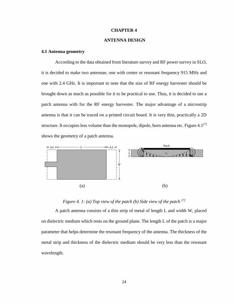
Figure 4. 1: (a) Top view of the patch (b) Side view of the patch [7]……………………… 24
Figure 4. 2: 2.4GHz patch antenna (a) layout of antenna (b)schematic of antenna…………. 27
Figure 4. 3: 915 MHz patch antenna (a) layout of antenna (b)schematic of antenna……… 27
Figure 4. 4: Magnitude and Phase plots for 2.4GHz antenna……………………………… 28
Figure 4. 5: Magnitude and Phase plots for 915MHz antenna……………………………… 28
Figure 4. 6: 3D view of far field radiation pattern for 2.4GHz antenna…………………… 29
Figure 4. 7: 3D view of far field radiation pattern for 915MHz antenna…………………… 29
Figure 4. 8: Antenna parameters vs frequency for 2.4GHz antenna………………………. 30
Figure 4. 9: Antenna parameters vs frequency for 915MHz antenna……………………… 31
Figure 4. 10: Impedance matching topologies [21]………………………………………… 33
Figure 4. 11: Series Capacitance, parallel inductance matching circuit [21]......................... 34
Figure 4. 12: Circuit to determine channel resistance of diode connected NMOS………… 35
Figure 4. 13: Model of matching network along with the source resistance and input
impedance for 915MHz antenna……………………………………………………………
36
Figure 4. 14: Frequency response of model shown in Figure 4.13…………………………. 37
Figure 4. 15: Model of matching network along with the source resistance and input
impedance for 2.4GHz antenna……………………………………………………………..
37
Figure 4. 16: Frequency response of model shown in Figure 4.15………………………… 38
Figure 5. 1: Single stage voltage doubler………………………………………………….. 40
Figure 5. 2: Transient response of single stage voltage doubler…………………………… 46
Figure 5. 3: Two stage voltage doubler……………………………………………………. 47
Figure 5. 4: Transient response of two stage voltage doubler……………………………… 47
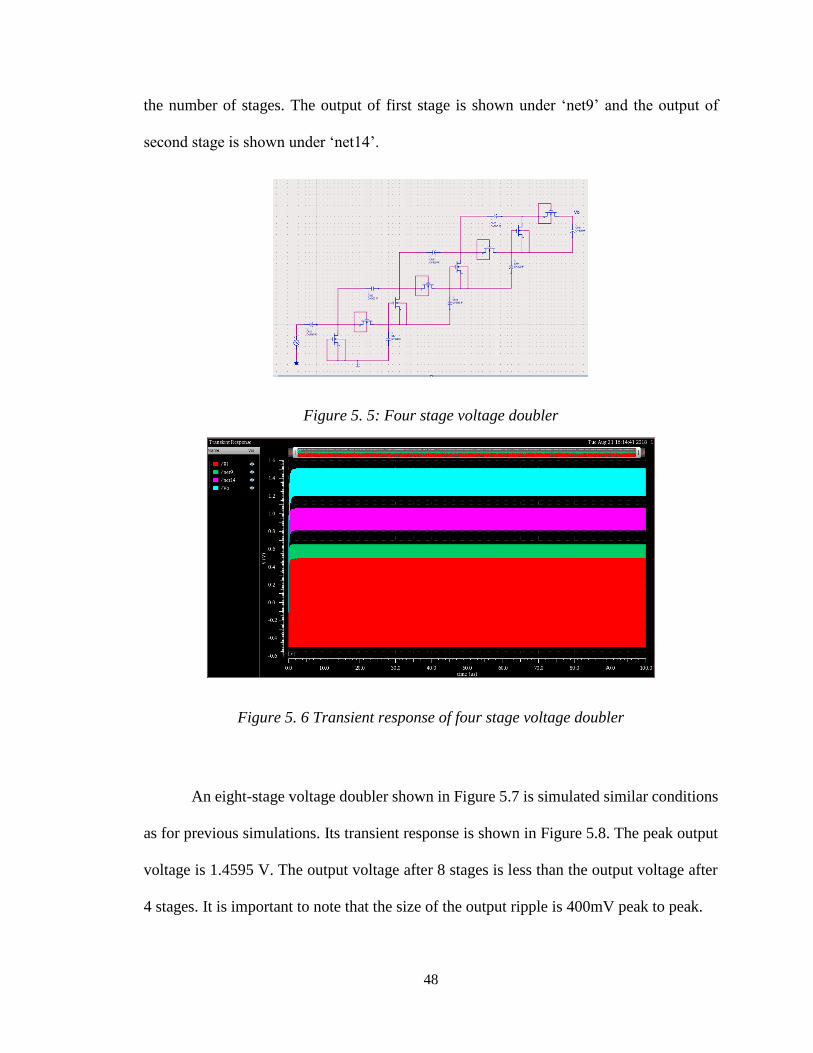
Figure 5. 5: Four stage voltage doubler……………………………………………………. 48
Figure 5. 6: Transient response of four stage voltage doubler…………………………….. 48
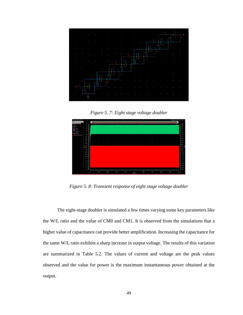
Figure 5. 7: Eight stage voltage doubler…………………………………………………… 49
Figure 5. 8: Transient response of eight stage voltage doubler……………………………. 49
Figure 5. 9: Transient response of final design…………………………………………….. 50
Figure 5. 10: (a) 3D view of NMOS structure (b) Structure of MIM and MIS capacitor
[32]…………………………………………………………………………………………
52
viii
Figure 5. 11: Layout of single stage of amplifier…………………………………………... 53
Figure 5. 12: Layout of the final eight stage amplifier…………………………………….. 53
Figure 5. 13: Final optimized layout……………………………………………………….. 54
Figure 7. 1: (a) Molex multi band ceramic chip antenna [36] (b) Abracon 915MHz ceramic
chip antenna [37]…………………………………………………………………………...
60
1
CHAPTER 1
INTRODUCTION
In the past few years, the field of low power wireless devices is rapidly increasing
in number. With the advent of IoT (Internet of Things) devices the number of wireless
devices has increased sharply. It is estimated that by 2020 the number of IoT devices in the
world would exceed 50 billion [4]. Wireless sensor networks, implantable and wearable
medical devices, low power data acquisition devices are a few examples of IoT devices
that consume very low power. Recent advances in these device technologies have
introduced devices which consume power in the range of micro-watts [1] [2] [3] [5].
RF (Radio Frequency) energy harvesting shows a lot of potential to provide energy
to these low power devices. It promises a power supply without the need to remove the
battery from the device for charging or replacement. The RF energy required for harvesting
can be provided manually or can be scavenged from existing RF sources in our
surroundings. Scavenging energy from existing RF sources provides us an inexpensive way
to power our devices without the need to set up additional infrastructure to facilitate our
technology.
The radio spectrum is divided into various bands by the governing body FCC
(Federal Communications Commission) [6]. Each of these bands serve a specific purpose
like Satellite communication, AM/FM broadcasting, TV broadcasting, cellular
communication, etc. Some of these frequency bands like the TV broadcasting and cellular
communication bands carry adequate amount of energy to satisfy our energy harvesting
2
goals of a few micro-watts. These bands are typically in the Ultra High Frequency (UHF)
domain, i.e. from 300MHz-3GHz [6].
While the number of IoT devices are increasing, the size of these devices is
decreasing. Thus, it is important to provide an energy harvesting solution that not only
matches the power requirement but is also small in size. The answer to designing a small
energy harvesting device lies in CMOS technology and Application Specific Integrated
Circuit (ASIC) design. CMOS technology offers transistor sizes as low as a few
nanometers and thus allows for an ASIC with a small footprint. This thesis presents the
design of a RF energy harvesting device aimed at powering some low power devices. The
device consists of an antenna, a matching circuit and the CMOS Amplifier IC. The design
uses Global Foundry’s 130nm 8RF CMOS technology for IC design and Keysight’s
Advanced Design Systems for Antenna Design.
The contents of this thesis can be summarized as follows. Chapter 2 provides
literature survey of the technology. It discusses results of past surveys of ambient RF
energy and various design methods involved in designing the rectifier amplifier circuit.
Chapter 3 provides a survey of ambient RF energy available for harvesting in San Luis
Obispo, CA. It discusses the survey methodology, results and draws conclusion on which
frequency bands need to be used for energy harvesting. Chapter 4 is aimed at antenna
design and the impedance matching network design. It gives details about important
antenna characteristics like radiation pattern, gain, efficiency, etc. as a function of
frequency. Chapter 5 presents the design of the rectifying and amplifying circuit. It

3
discusses various parameters that affect the output voltage and harvested power. It also
presents the layout of the final chip. Chapter 6 presents the conclusion of the thesis. Chapter
7 discusses the future scope of this thesis. It presents various ways to improve the existing
design or complement the design with other technologies to improve the performance
achieved in this thesis.
4
CHAPTER 2
LITERATURE SURVEY
2.1 Availability of RF energy
The study of ambient RF energy harvesting begins with determining the available
RF power in various frequency bands. The spatial distribution of RF energy sources
determines the available RF power at a given location. This can be seen from the Friis
transmission equation [7].
𝑃𝑟 = 𝑃𝑡𝐺𝑡𝐺𝑟𝜆2
(4𝜋𝑅)2
(Eq. 2.1)
Pr – received power
Pt – transmitted power
Gr – gain of the receiving antenna
Gt – gain of the transmitting antenna
λ – wavelength of the wave
R – distance between the transmitter and receiver
This equation relates the power received at a distance to the transmitted power. The
received power is inversely proportional to the square of the distance. Thus, the farther you
go from a transmitter, the amount of power received decreases quadratically. The available
RF power at any location depends on how far the location is from the transmitting station.
The spatial distribution of transmitting stations varies from city to city and as a result each
city has a unique distribution of power in various frequency bands. In the following section,
the results of RF power survey across multiple cities are studied. This information will help
determine the general trend of available RF power across various frequency bands.
5
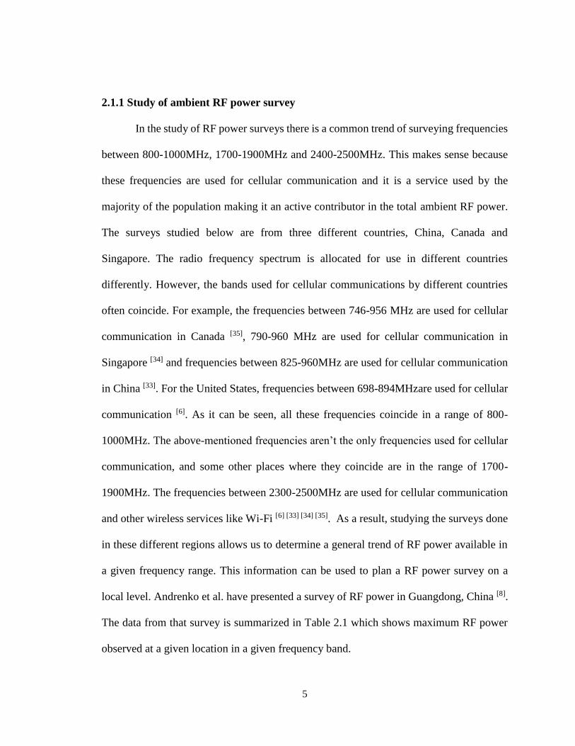
2.1.1 Study of ambient RF power survey
In the study of RF power surveys there is a common trend of surveying frequencies
between 800-1000MHz, 1700-1900MHz and 2400-2500MHz. This makes sense because
these frequencies are used for cellular communication and it is a service used by the
majority of the population making it an active contributor in the total ambient RF power.
The surveys studied below are from three different countries, China, Canada and
Singapore. The radio frequency spectrum is allocated for use in different countries
differently. However, the bands used for cellular communications by different countries
often coincide. For example, the frequencies between 746-956 MHz are used for cellular
communication in Canada [35], 790-960 MHz are used for cellular communication in
Singapore [34] and frequencies between 825-960MHz are used for cellular communication
in China [33]. For the United States, frequencies between 698-894MHzare used for cellular
communication [6]. As it can be seen, all these frequencies coincide in a range of 800-
1000MHz. The above-mentioned frequencies aren’t the only frequencies used for cellular
communication, and some other places where they coincide are in the range of 1700-
1900MHz. The frequencies between 2300-2500MHz are used for cellular communication
and other wireless services like Wi-Fi [6] [33] [34] [35]. As a result, studying the surveys done
in these different regions allows us to determine a general trend of RF power available in
a given frequency range. This information can be used to plan a RF power survey on a
local level. Andrenko et al. have presented a survey of RF power in Guangdong, China [8].
The data from that survey is summarized in Table 2.1 which shows maximum RF power
observed at a given location in a given frequency band.
6
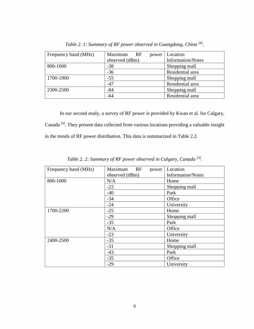
Table 2. 1: Summary of RF power observed in Guangdong, China [8].
Frequency band (MHz) Maximum RF power
observed (dBm)
Location
Information/Notes
800-1000 -38 Shopping mall
-36 Residential area
1700-1900 -55 Shopping mall
-47 Residential area
2300-2500 -84 Shopping mall
-64 Residential area
In our second study, a survey of RF power is provided by Kwan et al. for Calgary,
Canada [9]. They present data collected from various locations providing a valuable insight
in the trends of RF power distribution. This data is summarized in Table 2.2.
Table 2. 2: Summary of RF power observed in Calgary, Canada [9].
Frequency band (MHz) Maximum RF power
observed (dBm)
Location
Information/Notes
800-1000 N/A Home
-22 Shopping mall
-40 Park
-34 Office
-24 University
1700-2200 -25 Home
-29 Shopping mall
-35 Park
N/A Office
-23 University
2400-2500 -35 Home
-31 Shopping mall
-43 Park
-35 Office
-29 University
7
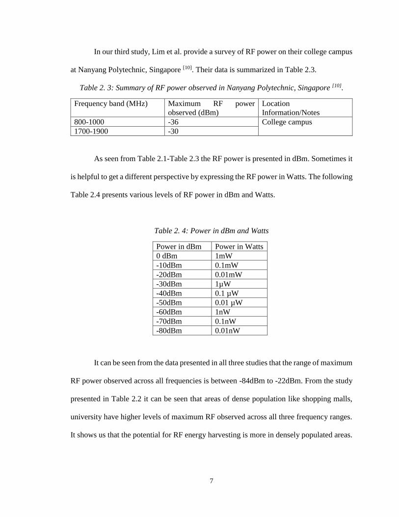
In our third study, Lim et al. provide a survey of RF power on their college campus
at Nanyang Polytechnic, Singapore [10]. Their data is summarized in Table 2.3.
Table 2. 3: Summary of RF power observed in Nanyang Polytechnic, Singapore [10].
Frequency band (MHz) Maximum RF power
observed (dBm)
Location
Information/Notes
800-1000 -36 College campus
1700-1900 -30
As seen from Table 2.1-Table 2.3 the RF power is presented in dBm. Sometimes it
is helpful to get a different perspective by expressing the RF power in Watts. The following
Table 2.4 presents various levels of RF power in dBm and Watts.
Table 2. 4: Power in dBm and Watts
Power in dBm Power in Watts
0 dBm 1mW
-10dBm 0.1mW
-20dBm 0.01mW
-30dBm 1µW
-40dBm 0.1 µW
-50dBm 0.01 µW
-60dBm 1nW
-70dBm 0.1nW
-80dBm 0.01nW
It can be seen from the data presented in all three studies that the range of maximum
RF power observed across all frequencies is between -84dBm to -22dBm. From the study
presented in Table 2.2 it can be seen that areas of dense population like shopping malls,
university have higher levels of maximum RF observed across all three frequency ranges.
It shows us that the potential for RF energy harvesting is more in densely populated areas.
8
2.1.2 Manual RF power source
The FCC has reserved some frequency bands for Industrial, Scientific and Medical
purposes. These are called the ISM bands and they are free to use by the public. There are
commercially available transmitters that operate at some of these frequencies, for example,
the Powercaster transmitter [12] which transmits at 915 MHz Some of the most commonly
used ISM frequencies are 434 MHz, 915 MHz, 2450 MHz. The commercially available
transmitters can also be used to power devices with RF energy harvesting capabilities.
However, the FCC has imposed some limits [13] on the amount of power that these devices
can transmit. The Powercaster comes with a limit of 3W [12]. These manual sources have a
range of about 15m within which the received power can be successfully harvested. This
would require a lot of these devices to cover a large area. This brings up the cost of initial
setup.
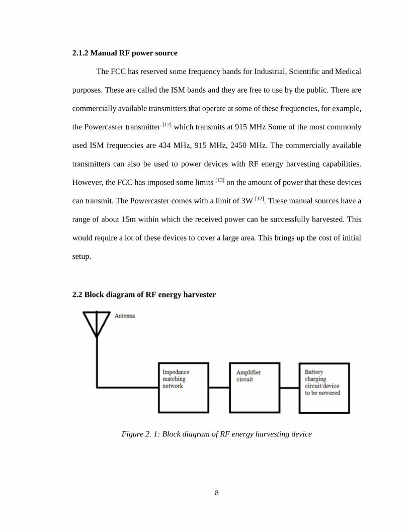
2.2 Block diagram of RF energy harvester
Figure 2. 1: Block diagram of RF energy harvesting device
9
The block diagram in Figure 2.1 presents a commonly used architecture for RF
energy harvesting devices [11]. The antenna responds to the incoming RF power and the
impedance matching network ensures maximum power transfer is achieved. The amplifier
circuit rectifies and amplifies the voltage of the received signal. It typically consists of
voltage multiplying circuits like the Villard voltage doubler or switched capacitor circuit
or the Dickson charge pump etc. The final stage is either to charge a battery or to provide
power directly to the device to be powered.
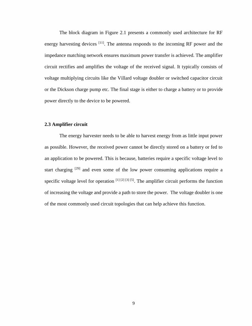
2.3 Amplifier circuit
The energy harvester needs to be able to harvest energy from as little input power
as possible. However, the received power cannot be directly stored on a battery or fed to
an application to be powered. This is because, batteries require a specific voltage level to
start charging [29] and even some of the low power consuming applications require a
specific voltage level for operation [1] [2] [3] [5]. The amplifier circuit performs the function
of increasing the voltage and provide a path to store the power. The voltage doubler is one
of the most commonly used circuit topologies that can help achieve this function.
10
Figure 2. 2: Villard voltage doubler [14]
During the negative half cycle of the sinusoidal input waveform, diode D1 is
forward biased and thus charges up the capacitor, C1 to the peak value of the input voltage,
Vi. Because there is no path for capacitor C1 to discharge into, it remains fully charged. At
the same time, diode D2 conducts via D1 charging up capacitor, C2. During the positive
half cycle, diode D1 is reverse biased blocking the discharging of C1while diode D2 is
forward biased charging up capacitor C2 and providing a path for capacitor C1 to
discharge. But because there is a voltage across capacitor C1 already equal to the peak
input voltage, capacitor C2 charges to twice the peak voltage value of the input signal. The
voltage across capacitor C2 is the output voltage Vo. Now the diodes have a small voltage
drop when they are forward biased so the capacitor C2 does not reach twice the input
voltage.
The output voltage Vo can be expressed as follows:
𝑉𝑜 = 2(𝑉𝑖 − ∆𝑉) (Eq. 2.2)
ΔV = voltage drop across the diode
11
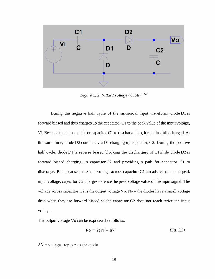
The output voltage is not instantaneous but increases slowly on each input cycle.
As capacitor C2 only charges up during one half cycle of the input waveform, the resulting
output voltage discharged into the load has a ripple frequency equal to the supply
frequency. However, the main advantage of this circuit topology is that they can be stacked
together in series to provide more voltage boost. The output voltage of an n-stage voltage
doubler circuit is given by the following equation.
𝑉𝑜 = 2𝑛(𝑉𝑖 − ∆𝑉) (Eq. 2.3)
This is assuming that all the diodes used are identical. This same circuit topology
can be realized in different ways as shown in Figure 2.3.
(a) (b)
Figure 2. 3: (a) Villard topology (b) Dickson topology [15]
According to [15] the two different topologies do not show any significant difference
in performance. However, the diodes available in 8RF technology are not suitable for this
design. There are two types of diodes available with 8RF technology, the forward-bias
diode and the Schottky barrier diode. The general use of forward biased diodes as circuit
elements is not supported in 8RF technology, while the Schottky barrier diode consumes
more area on chip than transistors and has higher forward bias voltage than the threshold
voltages of some of the transistors offered in 8RF technology. It can be seen from equation
12
2.2, higher forward bias voltage decreases the output voltage. Hence, we cannot use this
design for our device.
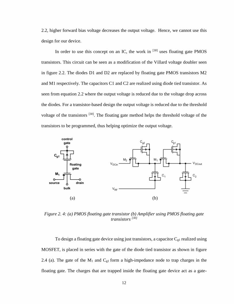
In order to use this concept on an IC, the work in [30] uses floating gate PMOS
transistors. This circuit can be seen as a modification of the Villard voltage doubler seen
in figure 2.2. The diodes D1 and D2 are replaced by floating gate PMOS transistors M2
and M1 respectively. The capacitors C1 and C2 are realized using diode tied transistor. As
seen from equation 2.2 where the output voltage is reduced due to the voltage drop across
the diodes. For a transistor-based design the output voltage is reduced due to the threshold
voltage of the transistors [30]. The floating gate method helps the threshold voltage of the
transistors to be programmed, thus helping optimize the output voltage.
(a) (b)
Figure 2. 4: (a) PMOS floating gate transistor (b) Amplifier using PMOS floating gate
transistors [30]
To design a floating gate device using just transistors, a capacitor Cg1 realized using
MOSFET, is placed in series with the gate of the diode tied transistor as shown in figure
2.4 (a). The gate of the M1 and Cg1 form a high-impedance node to trap charges in the
floating gate. The charges that are trapped inside the floating gate device act as a gate-
13
source bias to passively reduce the effective threshold voltage of the transistor. To create
the gate-source bias, a large sinusoidal signal is applied at the input of the rectifier. Charge
is injected into the floating gate via the parasitic capacitance between the gate-source and
gate-drain junction of the transistor and by hot electron effects. The sinusoidal signal can
be applied in pulses with peak voltages between 5–6 V with 2.5–3.0 V DC bias or by a
continuous train of signals at lower voltages and bias, depending on the duration of the
pulse train [30].
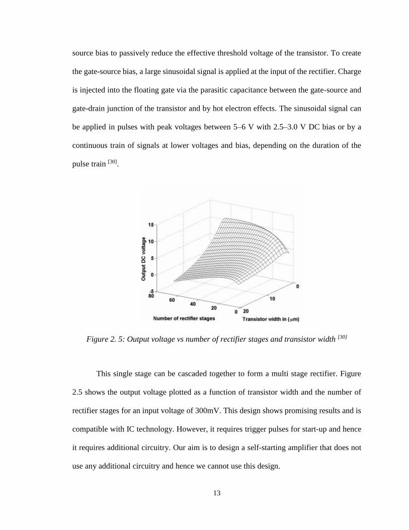
Figure 2. 5: Output voltage vs number of rectifier stages and transistor width [30]
This single stage can be cascaded together to form a multi stage rectifier. Figure
2.5 shows the output voltage plotted as a function of transistor width and the number of
rectifier stages for an input voltage of 300mV. This design shows promising results and is
compatible with IC technology. However, it requires trigger pulses for start-up and hence
it requires additional circuitry. Our aim is to design a self-starting amplifier that does not
use any additional circuitry and hence we cannot use this design.
14
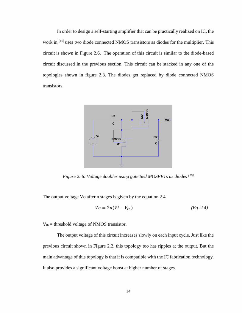
In order to design a self-starting amplifier that can be practically realized on IC, the
work in [16] uses two diode connected NMOS transistors as diodes for the multiplier. This
circuit is shown in Figure 2.6. The operation of this circuit is similar to the diode-based
circuit discussed in the previous section. This circuit can be stacked in any one of the
topologies shown in figure 2.3. The diodes get replaced by diode connected NMOS
transistors.
Figure 2. 6: Voltage doubler using gate tied MOSFETs as diodes [16]
The output voltage Vo after n stages is given by the equation 2.4
𝑉𝑜 = 2𝑛(𝑉𝑖 − 𝑉𝑡ℎ) (Eq. 2.4)
Vth = threshold voltage of NMOS transistor.
The output voltage of this circuit increases slowly on each input cycle. Just like the
previous circuit shown in Figure 2.2, this topology too has ripples at the output. But the
main advantage of this topology is that it is compatible with the IC fabrication technology.
It also provides a significant voltage boost at higher number of stages.
15
2.4 Solid state battery
The antenna, matching circuit and the amplifier together form an energy harvesting
device. It can be used to charge commercially available thin film or solid-state batteries.
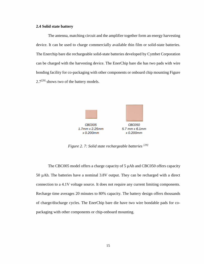
The Enerchip bare die rechargeable solid-state batteries developed by Cymbet Corporation
can be charged with the harvesting device. The EnerChip bare die has two pads with wire
bonding facility for co-packaging with other components or onboard chip mounting Figure
2.7[29] shows two of the battery models.
Figure 2. 7: Solid state rechargeable batteries [29]
The CBC005 model offers a charge capacity of 5 µAh and CBC050 offers capacity
50 µAh. The batteries have a nominal 3.8V output. They can be recharged with a direct
connection to a 4.1V voltage source. It does not require any current limiting components.
Recharge time averages 20 minutes to 80% capacity. The battery design offers thousands
of charge/discharge cycles. The EnerChip bare die have two wire bondable pads for co-
packaging with other components or chip-onboard mounting.
16
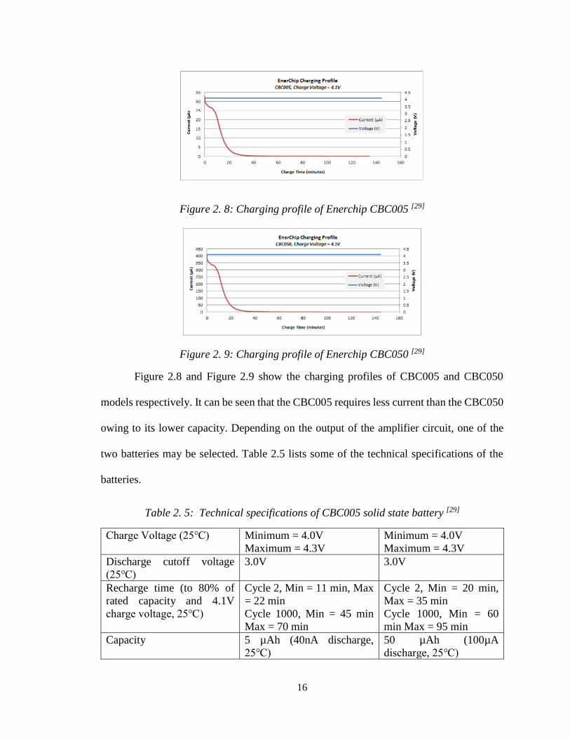
Figure 2. 8: Charging profile of Enerchip CBC005 [29]
Figure 2. 9: Charging profile of Enerchip CBC050 [29]
Figure 2.8 and Figure 2.9 show the charging profiles of CBC005 and CBC050
models respectively. It can be seen that the CBC005 requires less current than the CBC050
owing to its lower capacity. Depending on the output of the amplifier circuit, one of the
two batteries may be selected. Table 2.5 lists some of the technical specifications of the
batteries.
Table 2. 5: Technical specifications of CBC005 solid state battery [29]
Charge Voltage (25) Minimum = 4.0V
Maximum = 4.3V
Minimum = 4.0V
Maximum = 4.3V
Discharge cutoff voltage
(25)
3.0V 3.0V
Recharge time (to 80% of
rated capacity and 4.1V
charge voltage, 25)
Cycle 2, Min = 11 min, Max
= 22 min
Cycle 1000, Min = 45 min
Max = 70 min
Cycle 2, Min = 20 min,
Max = 35 min
Cycle 1000, Min = 60
min Max = 95 min
Capacity 5 µAh (40nA discharge,
25)
50 µAh (100µA
discharge, 25)
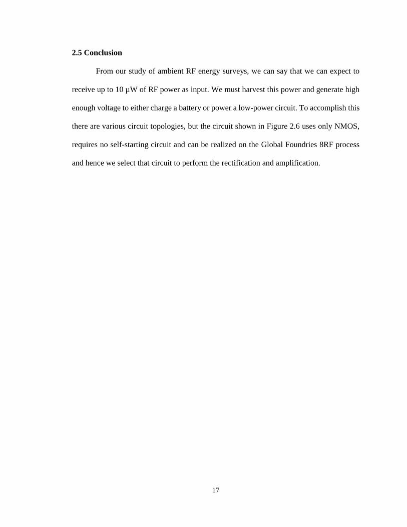
17
2.5 Conclusion
From our study of ambient RF energy surveys, we can say that we can expect to
receive up to 10 µW of RF power as input. We must harvest this power and generate high
enough voltage to either charge a battery or power a low-power circuit. To accomplish this
there are various circuit topologies, but the circuit shown in Figure 2.6 uses only NMOS,
requires no self-starting circuit and can be realized on the Global Foundries 8RF process
and hence we select that circuit to perform the rectification and amplification.
18
CHAPTER 3
RF POWER SURVEY
3.1 Study of cellular communication frequency bands
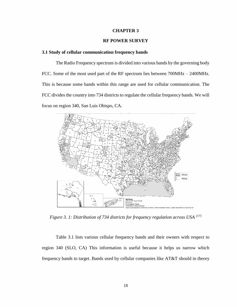
The Radio Frequency spectrum is divided into various bands by the governing body
FCC. Some of the most used part of the RF spectrum lies between 700MHz – 2400MHz.
This is because some bands within this range are used for cellular communication. The
FCC divides the country into 734 districts to regulate the cellular frequency bands. We will
focus on region 340, San Luis Obispo, CA.
Figure 3. 1: Distribution of 734 districts for frequency regulation across USA [17]
Table 3.1 lists various cellular frequency bands and their owners with respect to
region 340 (SLO, CA) This information is useful because it helps us narrow which
frequency bands to target. Bands used by cellular companies like AT&T should in theory
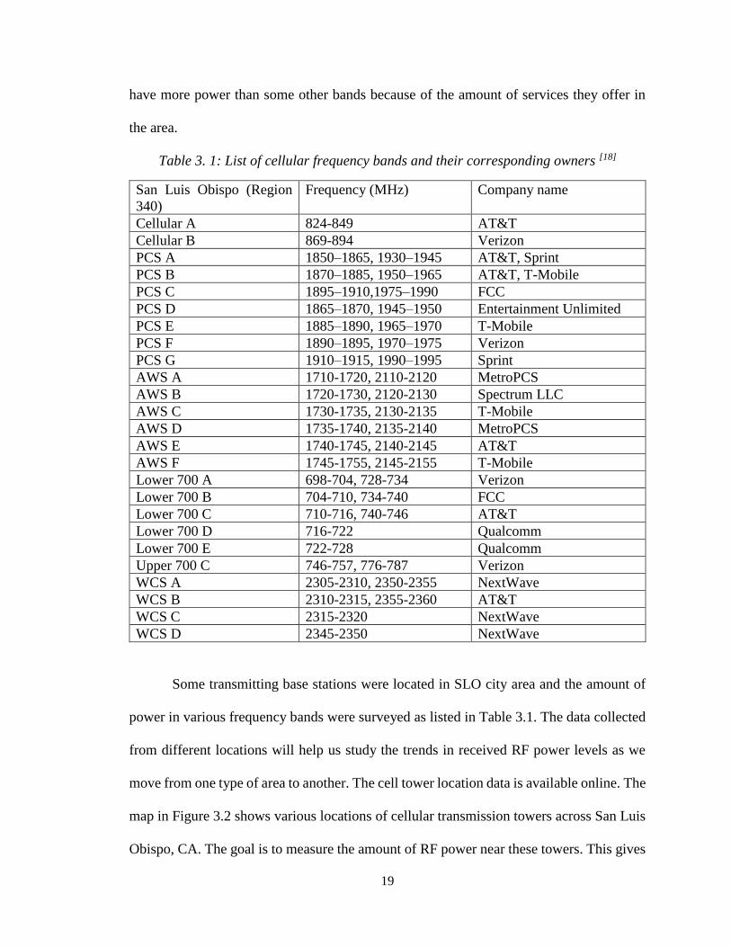
19
have more power than some other bands because of the amount of services they offer in
the area.
Table 3. 1: List of cellular frequency bands and their corresponding owners [18]
San Luis Obispo (Region
340)
Frequency (MHz) Company name
Cellular A 824-849 AT&T
Cellular B 869-894 Verizon
PCS A 1850–1865, 1930–1945 AT&T, Sprint
PCS B 1870–1885, 1950–1965 AT&T, T-Mobile
PCS C 1895–1910,1975–1990 FCC
PCS D 1865–1870, 1945–1950 Entertainment Unlimited
PCS E 1885–1890, 1965–1970 T-Mobile
PCS F 1890–1895, 1970–1975 Verizon
PCS G 1910–1915, 1990–1995 Sprint
AWS A 1710-1720, 2110-2120 MetroPCS
AWS B 1720-1730, 2120-2130 Spectrum LLC
AWS C 1730-1735, 2130-2135 T-Mobile
AWS D 1735-1740, 2135-2140 MetroPCS
AWS E 1740-1745, 2140-2145 AT&T
AWS F 1745-1755, 2145-2155 T-Mobile
Lower 700 A 698-704, 728-734 Verizon
Lower 700 B 704-710, 734-740 FCC
Lower 700 C 710-716, 740-746 AT&T
Lower 700 D 716-722 Qualcomm
Lower 700 E 722-728 Qualcomm
Upper 700 C 746-757, 776-787 Verizon
WCS A 2305-2310, 2350-2355 NextWave
WCS B 2310-2315, 2355-2360 AT&T
WCS C 2315-2320 NextWave
WCS D 2345-2350 NextWave
Some transmitting base stations were located in SLO city area and the amount of
power in various frequency bands were surveyed as listed in Table 3.1. The data collected
from different locations will help us study the trends in received RF power levels as we
move from one type of area to another. The cell tower location data is available online. The
map in Figure 3.2 shows various locations of cellular transmission towers across San Luis
Obispo, CA. The goal is to measure the amount of RF power near these towers. This gives
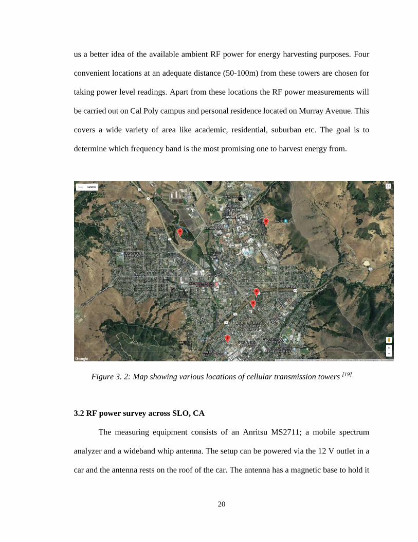
20
us a better idea of the available ambient RF power for energy harvesting purposes. Four
convenient locations at an adequate distance (50-100m) from these towers are chosen for
taking power level readings. Apart from these locations the RF power measurements will
be carried out on Cal Poly campus and personal residence located on Murray Avenue. This
covers a wide variety of area like academic, residential, suburban etc. The goal is to
determine which frequency band is the most promising one to harvest energy from.
Figure 3. 2: Map showing various locations of cellular transmission towers [19]
3.2 RF power survey across SLO, CA
The measuring equipment consists of an Anritsu MS2711; a mobile spectrum
analyzer and a wideband whip antenna. The setup can be powered via the 12 V outlet in a
car and the antenna rests on the roof of the car. The antenna has a magnetic base to hold it
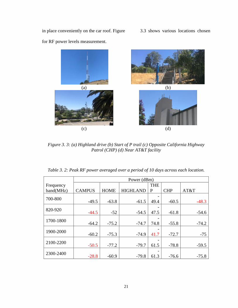
21
in place conveniently on the car roof. Figure 3.3 shows various locations chosen
for RF power levels measurement.
(a) (b)
(c) (d)
Figure 3. 3: (a) Highland drive (b) Start of P trail (c) Opposite California Highway
Patrol (CHP) (d) Near AT&T facility
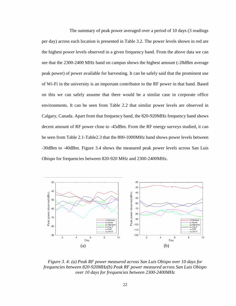
Table 3. 2: Peak RF power averaged over a period of 10 days across each location.
Frequency
band(MHz)
Power (dBm)
CAMPUS HOME HIGHLAND
THE
P CHP AT&T
700-800
-49.5 -63.8 -61.5
-
49.4 -60.5 -48.3
820-920 -44.5 -52 -54.5
-
47.5 -61.8 -54.6
1700-1800 -64.2 -75.2 -74.7
-
74.8 -55.8 -74.2
1900-2000 -60.2 -75.3 -74.9
-
41.7 -72.7 -75
2100-2200 -50.5 -77.2 -79.7
-
61.5 -78.8 -59.5
2300-2400 -28.8 -60.9 -79.8
-
61.3 -76.6 -75.8
22
The summary of peak power averaged over a period of 10 days (3 readings
per day) across each location is presented in Table 3.2. The power levels shown in red are
the highest power levels observed in a given frequency band. From the above data we can
see that the 2300-2400 MHz band on campus shows the highest amount (-28dBm average
peak power) of power available for harvesting. It can be safely said that the prominent use
of Wi-Fi in the university is an important contributor to the RF power in that band. Based
on this we can safely assume that there would be a similar case in corporate office
environments. It can be seen from Table 2.2 that similar power levels are observed in
Calgary, Canada. Apart from that frequency band, the 820-920MHz frequency band shows
decent amount of RF power close to -45dBm. From the RF energy surveys studied, it can
be seen from Table 2.1-Table2.3 that the 800-1000MHz band shows power levels between
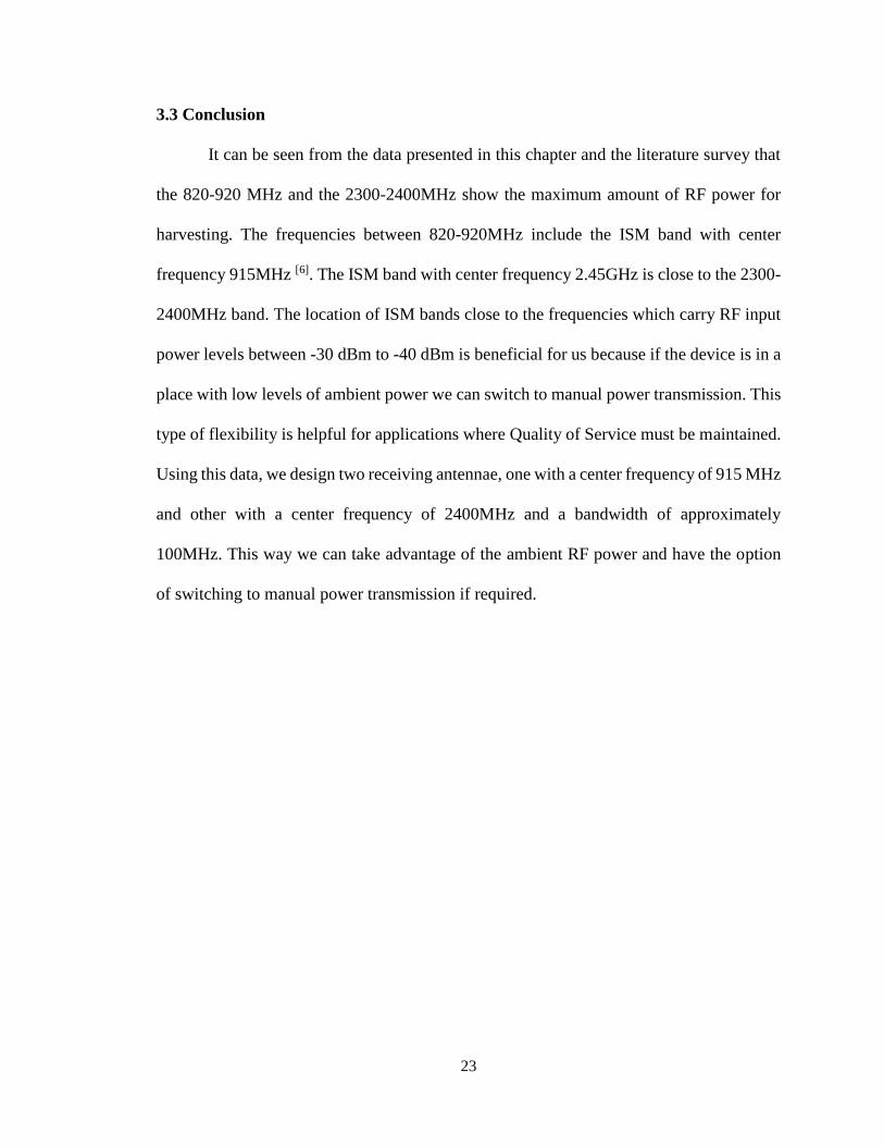
-30dBm to -40dBm. Figure 3.4 shows the measured peak power levels across San Luis
Obispo for frequencies between 820-920 MHz and 2300-2400MHz.
(a) (b)
Figure 3. 4: (a) Peak RF power measured across San Luis Obispo over 10 days for
frequencies between 820-920MHz(b) Peak RF power measured across San Luis Obispo
over 10 days for frequencies between 2300-2400MHz
23
3.3 Conclusion
It can be seen from the data presented in this chapter and the literature survey that
the 820-920 MHz and the 2300-2400MHz show the maximum amount of RF power for
harvesting. The frequencies between 820-920MHz include the ISM band with center
frequency 915MHz [6]. The ISM band with center frequency 2.45GHz is close to the 2300-
2400MHz band. The location of ISM bands close to the frequencies which carry RF input
power levels between -30 dBm to -40 dBm is beneficial for us because if the device is in a
place with low levels of ambient power we can switch to manual power transmission. This
type of flexibility is helpful for applications where Quality of Service must be maintained.
Using this data, we design two receiving antennae, one with a center frequency of 915 MHz
and other with a center frequency of 2400MHz and a bandwidth of approximately
100MHz. This way we can take advantage of the ambient RF power and have the option
of switching to manual power transmission if required.
24
CHAPTER 4
ANTENNA DESIGN
4.1 Antenna geometry
According to the data obtained from literature survey and RF power survey in SLO,
it is decided to make two antennae, one with center or resonant frequency 915 MHz and
one with 2.4 GHz. It is important to note that the size of RF energy harvester should be
brought down as much as possible for it to be practical to use. Thus, it is decided to use a
patch antenna with for the RF energy harvester. The major advantage of a microstrip
antenna is that it can be traced on a printed circuit board. It is very thin, practically a 2D
structure. It occupies less volume than the monopole, dipole, horn antenna etc. Figure 4.1[7]
shows the geometry of a patch antenna.
(a) (b)
Figure 4. 1: (a) Top view of the patch (b) Side view of the patch [7]
A patch antenna consists of a thin strip of metal of length L and width W, placed
on dielectric medium which rests on the ground plane. The length L of the patch is a major
parameter that helps determine the resonant frequency of the antenna. The thickness of the
metal strip and thickness of the dielectric medium should be very less than the resonant
wavelength.
25
4.2 Antenna parameters calculation
The design of a patch antenna begins with determining a good substrate. The
dielectric constant of the substrate should be low, and thickness of the substrate should be
high for better efficiency [7]. However, thicker substrates have higher amount of surface
waves. Surface waves do not radiate and are attenuated through the dielectric which causes
loss of power and efficiency [7]. The most commonly used FR4 substrate is selected due to
its low dielectric constant. It has a dielectric constant of 4.4. The substrate comes in various
levels of thickness, so we can choose a value that gives us high efficiency. The dimensions
of the patch antenna to be designed are given by the following set of equations. These
equations are derived in [7].
𝑊 = 1
2𝑓𝑟√µ0𝜀0
√2
𝜀𝑟 + 1
(Eq. 4.1)
𝜀𝑟𝑒𝑓𝑓 = 𝜀𝑟 + 1
2+
𝜀𝑟 − 1
2[1 + 12
ℎ
𝑊]−
12
(Eq. 4.2)
𝛥𝐿 = 0.412ℎ(𝜀𝑟𝑒𝑓𝑓 + 0.3) (
𝑊ℎ
+ 0.264)
(𝜀𝑟𝑒𝑓𝑓 − 0.258) (𝑊ℎ
+ 0.8)
(Eq. 4.3)
𝐿 = 1
2𝑓𝑟√𝜀𝑟𝑒𝑓𝑓µ0𝜀0
− 2 𝛥𝐿 (Eq. 4.4)
W = Width of the patch, L = Length of the patch, ΔL = Length of the extension
fr = Resonant frequency of the antenna, εr = Dielectric constant of the substrate
εreff = Effective dielectric constant of the substrate, h = thickness of the dielectric
26
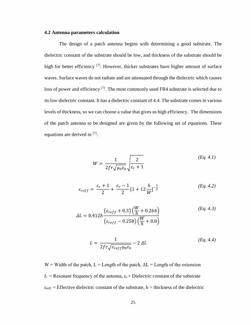
This design shows the microstrip feedline connected to the edge of the patch. The
feedline can be modified to move into the patch by a distance R. This modified antenna
has lower input impedance and hence higher current. The reduced impedance is given by
equation 4.5 [7]
𝑍𝑖𝑛 = 𝑐𝑜𝑠2 (𝜋𝑅
𝐿) 𝑍0
(Eq. 4.5)
Zin = Input impedance of modified feedline
Z0 = Input impedance of feedline at the edge of the patch
h = 1.5mm, ɛr = 4.4
Table 4. 1: Calculated dimensions of both the antennas to be designed.
Parameter 915 MHz 2.4 GHz
W 99.77 mm 38 mm
L 76.88 mm 28.72
ΔL 0.7 mm 0.7 mm
R 10 mm 6 mm
4.3 Antenna design and simulation on ADS
The dimensions of the antenna to be designed are calculated from the given
equations. The calculated values are showed in Table 4.1. The dimensions are calculated
for a patch antenna with feed on the edge. To design and simulate the antenna, Advanced
Design System software is used. While using the software for simulation, the feedline is
modified to move into the patch by a distance R. This helps reduce the antenna dimensions
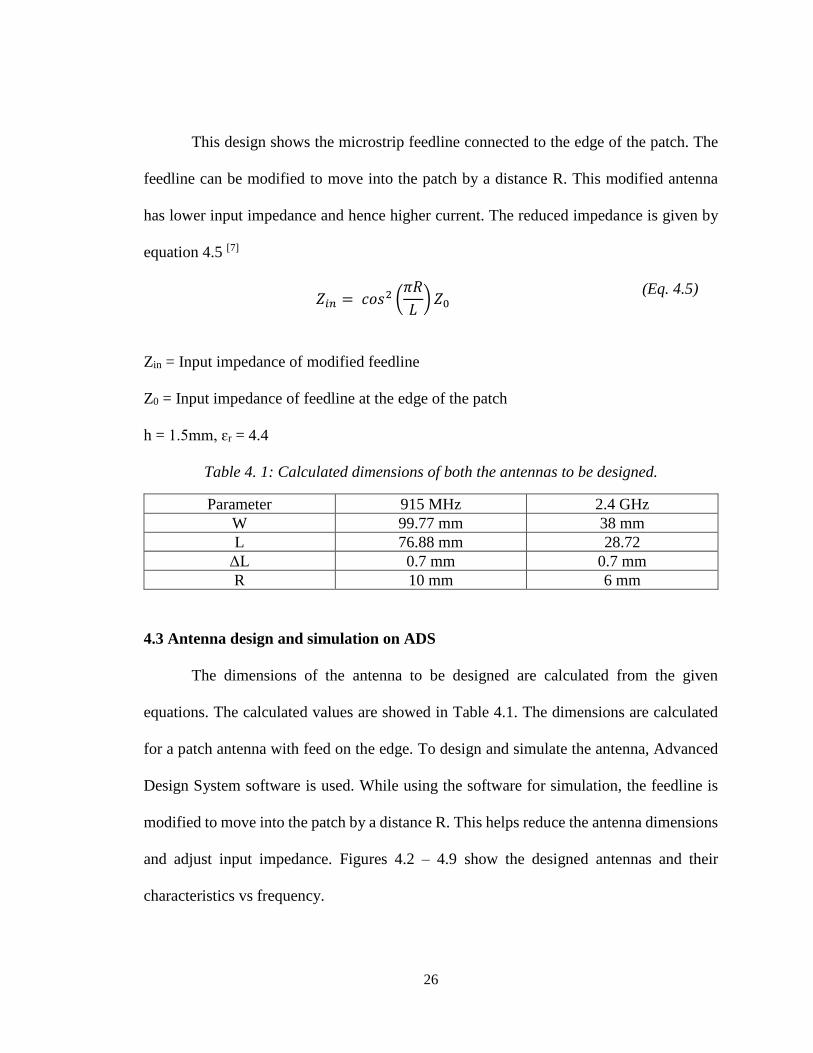
and adjust input impedance. Figures 4.2 – 4.9 show the designed antennas and their
characteristics vs frequency.
27
(a) (b)
Figure 4. 2: 2.4GHz patch antenna (a) layout of antenna (b) schematic of antenna
(a) (b)
Figure 4. 3: 915 MHz patch antenna (a) layout of antenna (b) schematic of antenna
Figure 4.2 shows layout and schematic of the 2.4GHz antenna. The antenna
simulation is started with the calculated dimensions and then the dimensions are adjusted
during the simulation to obtain desired bandwidth and center frequency. The feedline is
6mm long and 8mm wide. It has an impedance of 37.59Ω. Figure 4.3 shows layout and
schematic of the 915MHz antenna. The feedline for this antenna is 10mm long and 40mm
wide. It has an impedance of 6.7 Ω.
28
Figure 4. 4: Magnitude and Phase plots for 2.4GHz antenna
Figure 4. 5: Magnitude and Phase plots for 915MHz antenna
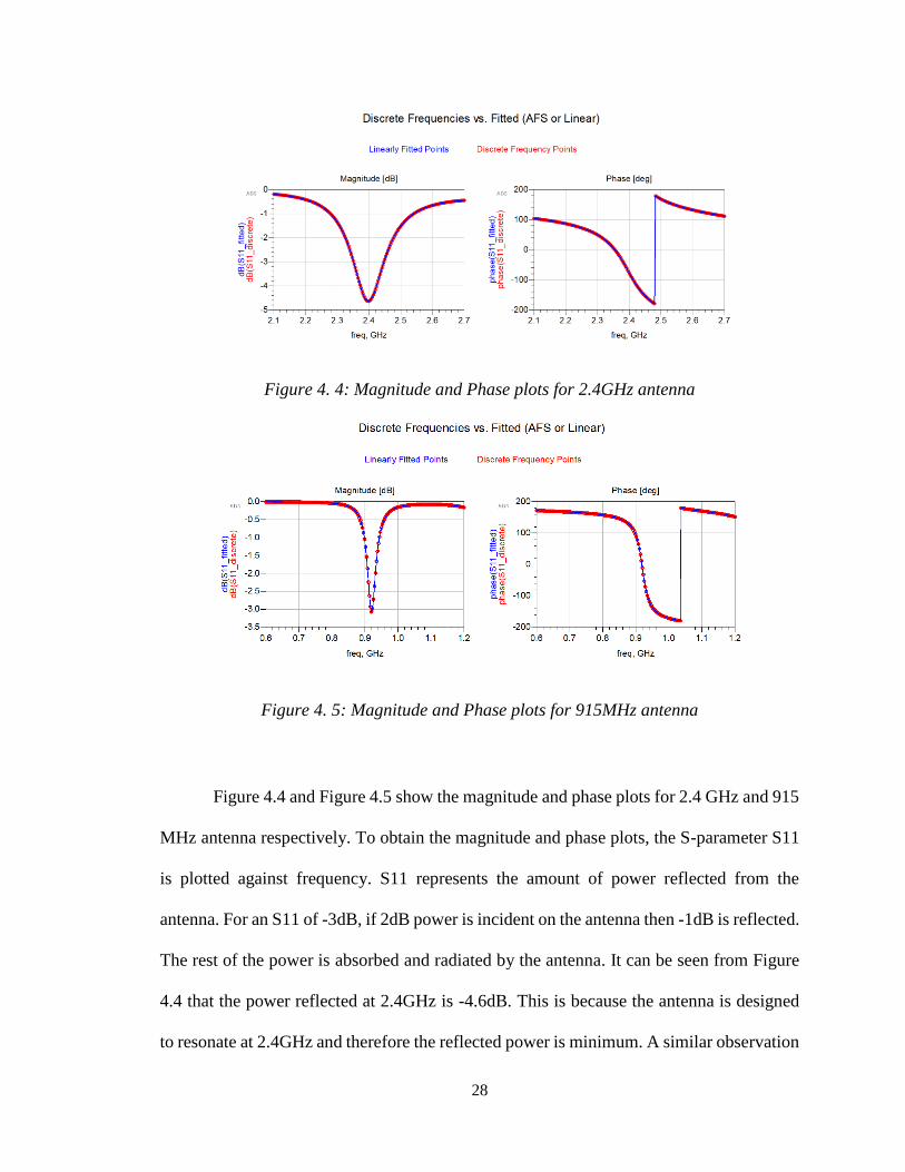
Figure 4.4 and Figure 4.5 show the magnitude and phase plots for 2.4 GHz and 915
MHz antenna respectively. To obtain the magnitude and phase plots, the S-parameter S11
is plotted against frequency. S11 represents the amount of power reflected from the
antenna. For an S11 of -3dB, if 2dB power is incident on the antenna then -1dB is reflected.
The rest of the power is absorbed and radiated by the antenna. It can be seen from Figure
4.4 that the power reflected at 2.4GHz is -4.6dB. This is because the antenna is designed
to resonate at 2.4GHz and therefore the reflected power is minimum. A similar observation
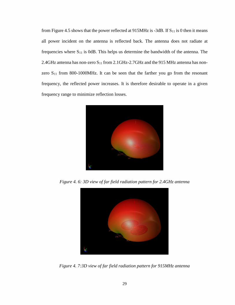
29
from Figure 4.5 shows that the power reflected at 915MHz is -3dB. If S11 is 0 then it means
all power incident on the antenna is reflected back. The antenna does not radiate at
frequencies where S11 is 0dB. This helps us determine the bandwidth of the antenna. The
2.4GHz antenna has non-zero S11 from 2.1GHz-2.7GHz and the 915 MHz antenna has non-
zero S11 from 800-1000MHz. It can be seen that the farther you go from the resonant
frequency, the reflected power increases. It is therefore desirable to operate in a given
frequency range to minimize reflection losses.
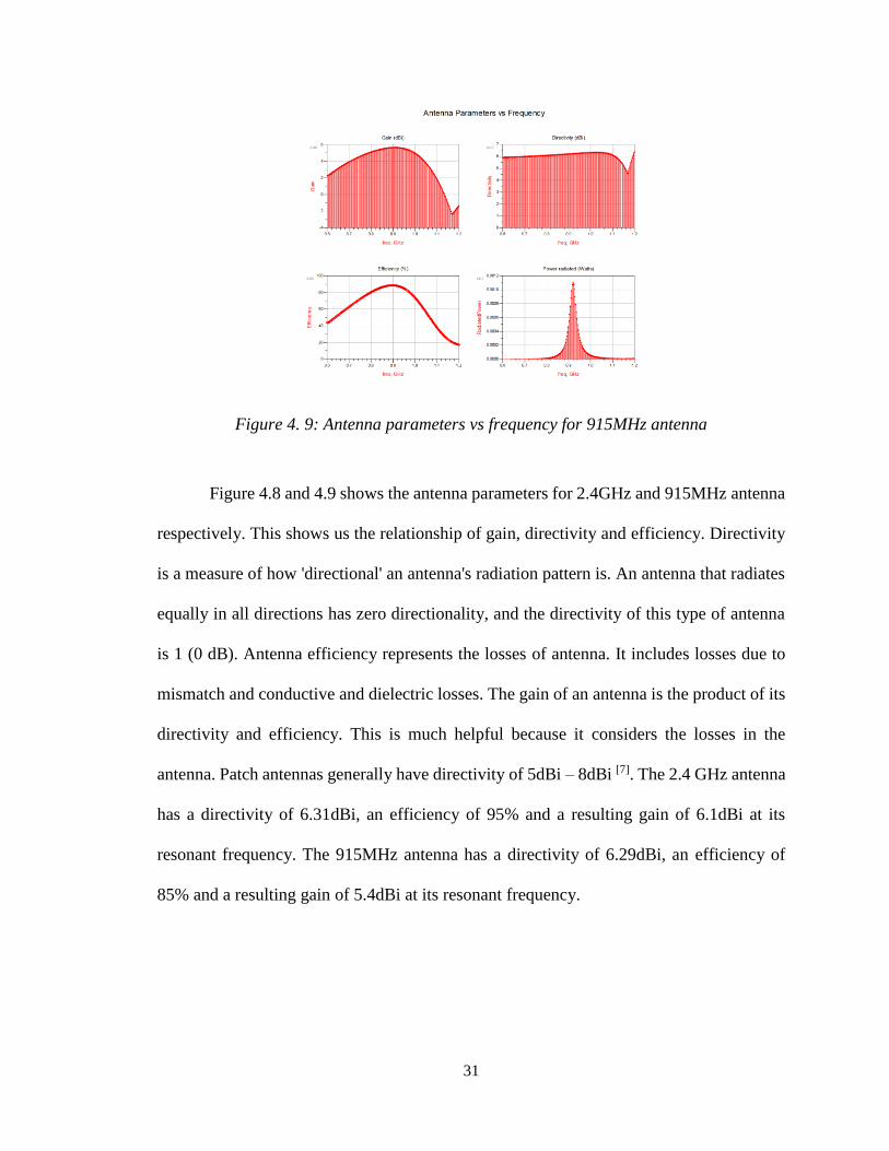
Figure 4. 6: 3D view of far field radiation pattern for 2.4GHz antenna
Figure 4. 7:3D view of far field radiation pattern for 915MHz antenna
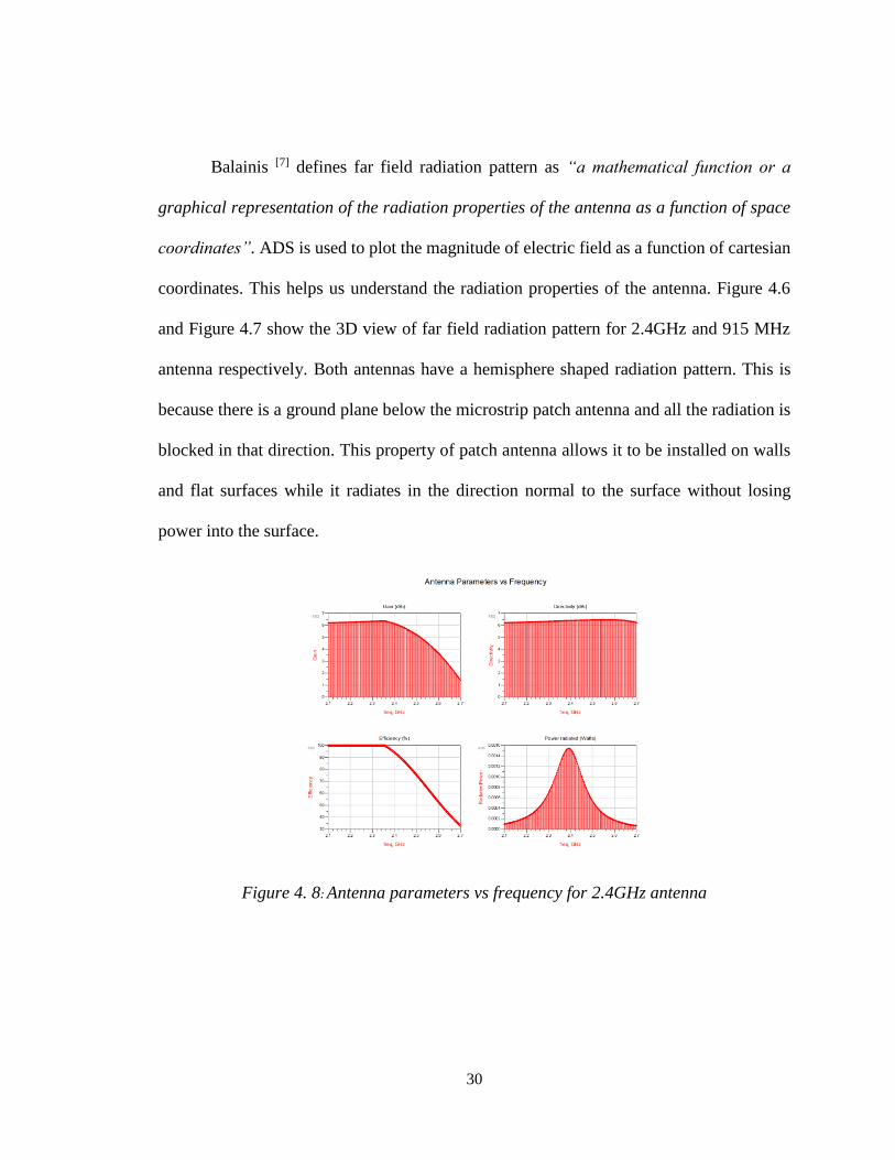
30
Balainis [7] defines far field radiation pattern as “a mathematical function or a
graphical representation of the radiation properties of the antenna as a function of space
coordinates”. ADS is used to plot the magnitude of electric field as a function of cartesian
coordinates. This helps us understand the radiation properties of the antenna. Figure 4.6
and Figure 4.7 show the 3D view of far field radiation pattern for 2.4GHz and 915 MHz
antenna respectively. Both antennas have a hemisphere shaped radiation pattern. This is
because there is a ground plane below the microstrip patch antenna and all the radiation is
blocked in that direction. This property of patch antenna allows it to be installed on walls
and flat surfaces while it radiates in the direction normal to the surface without losing
power into the surface.
Figure 4. 8: Antenna parameters vs frequency for 2.4GHz antenna
31
Figure 4. 9: Antenna parameters vs frequency for 915MHz antenna
Figure 4.8 and 4.9 shows the antenna parameters for 2.4GHz and 915MHz antenna
respectively. This shows us the relationship of gain, directivity and efficiency. Directivity
is a measure of how 'directional' an antenna's radiation pattern is. An antenna that radiates
equally in all directions has zero directionality, and the directivity of this type of antenna
is 1 (0 dB). Antenna efficiency represents the losses of antenna. It includes losses due to
mismatch and conductive and dielectric losses. The gain of an antenna is the product of its
directivity and efficiency. This is much helpful because it considers the losses in the
antenna. Patch antennas generally have directivity of 5dBi – 8dBi [7]. The 2.4 GHz antenna
has a directivity of 6.31dBi, an efficiency of 95% and a resulting gain of 6.1dBi at its
resonant frequency. The 915MHz antenna has a directivity of 6.29dBi, an efficiency of
85% and a resulting gain of 5.4dBi at its resonant frequency.
32
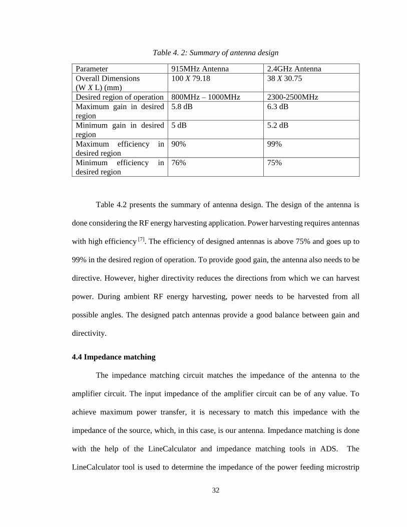
Table 4. 2: Summary of antenna design
Parameter 915MHz Antenna 2.4GHz Antenna
Overall Dimensions
(W X L) (mm)
100 X 79.18 38 X 30.75
Desired region of operation 800MHz – 1000MHz 2300-2500MHz
Maximum gain in desired
region
5.8 dB 6.3 dB
Minimum gain in desired
region
5 dB 5.2 dB
Maximum efficiency in
desired region
90% 99%
Minimum efficiency in
desired region
76% 75%
Table 4.2 presents the summary of antenna design. The design of the antenna is
done considering the RF energy harvesting application. Power harvesting requires antennas
with high efficiency [7]. The efficiency of designed antennas is above 75% and goes up to
99% in the desired region of operation. To provide good gain, the antenna also needs to be
directive. However, higher directivity reduces the directions from which we can harvest
power. During ambient RF energy harvesting, power needs to be harvested from all
possible angles. The designed patch antennas provide a good balance between gain and
directivity.
4.4 Impedance matching
The impedance matching circuit matches the impedance of the antenna to the
amplifier circuit. The input impedance of the amplifier circuit can be of any value. To
achieve maximum power transfer, it is necessary to match this impedance with the
impedance of the source, which, in this case, is our antenna. Impedance matching is done
with the help of the LineCalculator and impedance matching tools in ADS. The
LineCalculator tool is used to determine the impedance of the power feeding microstrip
33
line which connects the antenna to the rectifier circuit. We can call this our source
impedance as it is directly attached to the antenna. The input impedance of the amplifier
circuit is the load impedance Z to be matched with the source impedance. A matching
network can be designed to be placed in between the source, antenna and the load, amplifier
circuit. ADS impedance matching tools are used to design a matching network.
The first step involves measuring the source impedance and determining a matching
network topology. It can be calculated using LineCalculator that the impedance value is
6.75Ω for a 10mmX40mm microstrip feedline used with the 915 MHz antenna. Similar
calculation for the 2.4 GHz antenna gives input impedance as 37.59Ω for an 8mmX6mm
microstrip feedline used with the antenna. The impedance of the microstrip feedline is
resistive in nature.
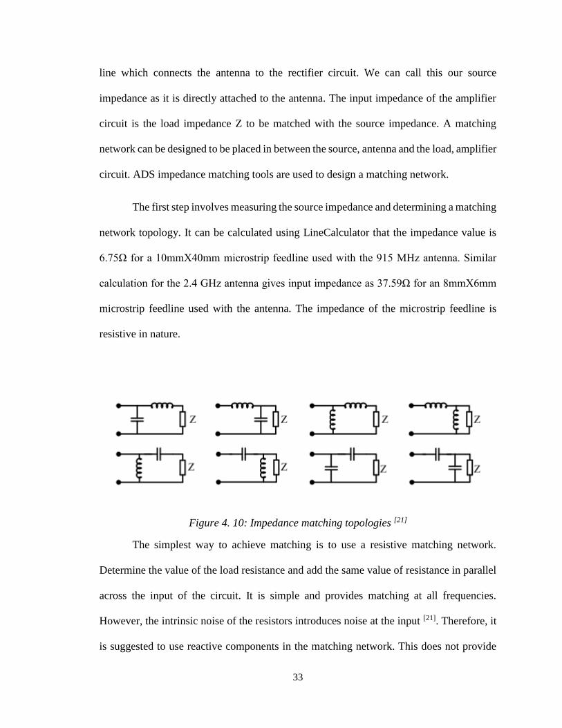
Figure 4. 10: Impedance matching topologies [21]
The simplest way to achieve matching is to use a resistive matching network.
Determine the value of the load resistance and add the same value of resistance in parallel
across the input of the circuit. It is simple and provides matching at all frequencies.
However, the intrinsic noise of the resistors introduces noise at the input [21]. Therefore, it
is suggested to use reactive components in the matching network. This does not provide
34
wideband matching like the resistors, but it also does not introduce as much noise [21]. A
matching network using reactive components can be designed for a given band of
frequencies. We want to achieve impedance matching for a center frequency of 915 MHz
or 2.4 GHz depending on the frequency selected to harvest RF power. With the proper
choice of two reactive components, any impedance can be matched. There are eight
possible two component matching networks, also known as ell networks, shown in Figure
4.10. The selection of a proper matching circuit depends on which circuit provides
reasonable component values, personal preference, or stability criteria. In our case, we are
working at high frequencies and our main goal is to design a matching network that is also
suitable with our power harvesting goals. We require a high pass network, so we cannot
choose a circuit where the capacitor is connected to ground because at high frequencies it
acts as a short and attenuates all the power received. We select the circuit with series
capacitor and parallel inductor shown in Figure 4.11. Z represents load, which in our case
is the amplifier circuit.
Figure 4. 11: Series Capacitance, parallel inductance matching circuit [21].
Now, the second step in impedance matching is to determine the load impedance.
This information, along with the information of the source impedance is used by the
impedance matching tools in ADS to automatically design a matching network. It can be
seen from figure 5.7 that for our final amplifier design, the input impedance is due to the
capacitance of CM0 and channel resistance of NMOS T0 of the first stage voltage doubler.
35
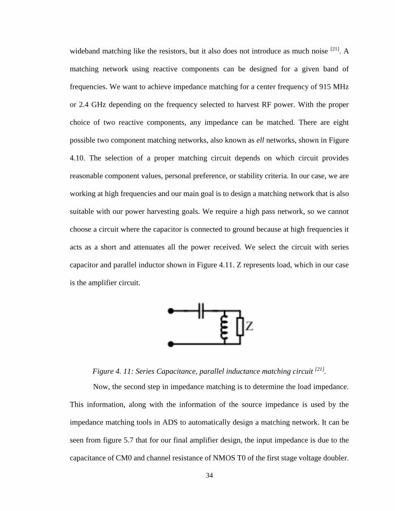
The components can be clearly seen in Figure 5.1 which shows single stage voltage
doubler. The value of capacitance is designed to be 3.57pF. The channel resistance of the
diode connected NMOS is determined using a separate circuit simulated on Virtuoso.
Figure 4.12 shows the circuit used to determine channel resistance of NMOS.
Figure 4. 12: Circuit to determine channel resistance of diode connected NMOS
The circuit is simulated for an input of 500mV sine wave of frequency 915MHz.
The input resistance is calculated using the formula given in equation 4.6. V(t) and I(t)
represent the voltage and current across the diode tied NMOS. The Cadence simulator has
N samples of V(t) and I(t) stored from time t0 to time tn. The VIVA calculator is used to
obtain the value of input impedance. The value of Zrms is calculated to be 17.35kΩ. The
input impedance can be modeled with a capacitor of 3.57pF and a resistance of 17.35kΩ.
𝑍𝑟𝑚𝑠 =𝑉𝑟𝑚𝑠
𝐼𝑟𝑚𝑠=
1𝑁 √∑ 𝑉2(𝑡)𝑡𝑛
𝑡=𝑡0
1𝑁 √∑ 𝐼2(𝑡)𝑡𝑛
𝑡=𝑡0
(Eq. 4.6)
36
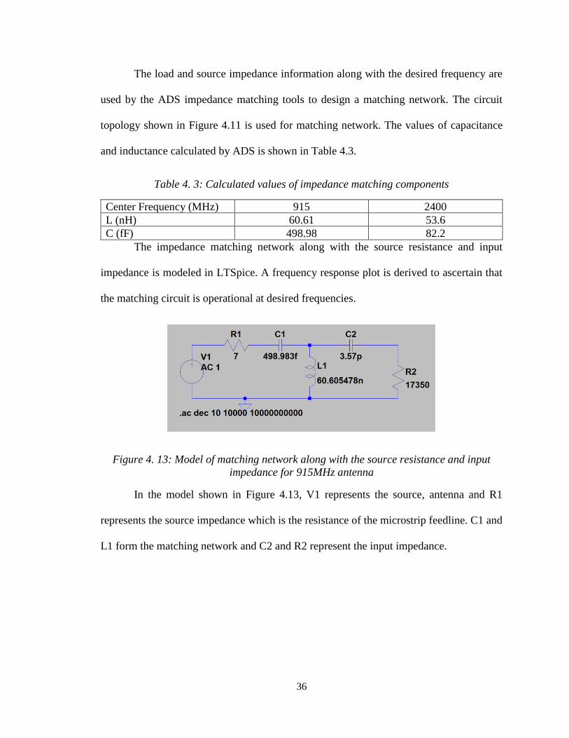
The load and source impedance information along with the desired frequency are
used by the ADS impedance matching tools to design a matching network. The circuit
topology shown in Figure 4.11 is used for matching network. The values of capacitance
and inductance calculated by ADS is shown in Table 4.3.
Table 4. 3: Calculated values of impedance matching components
Center Frequency (MHz) 915 2400
L (nH) 60.61 53.6
C (fF) 498.98 82.2
The impedance matching network along with the source resistance and input
impedance is modeled in LTSpice. A frequency response plot is derived to ascertain that
the matching circuit is operational at desired frequencies.
Figure 4. 13: Model of matching network along with the source resistance and input
impedance for 915MHz antenna
In the model shown in Figure 4.13, V1 represents the source, antenna and R1
represents the source impedance which is the resistance of the microstrip feedline. C1 and
L1 form the matching network and C2 and R2 represent the input impedance.
37
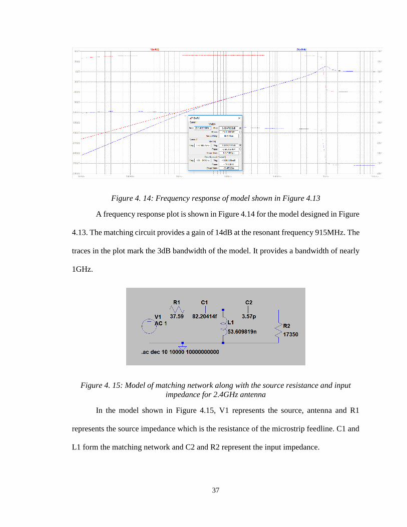
Figure 4. 14: Frequency response of model shown in Figure 4.13
A frequency response plot is shown in Figure 4.14 for the model designed in Figure
4.13. The matching circuit provides a gain of 14dB at the resonant frequency 915MHz. The
traces in the plot mark the 3dB bandwidth of the model. It provides a bandwidth of nearly
1GHz.
Figure 4. 15: Model of matching network along with the source resistance and input
impedance for 2.4GHz antenna
In the model shown in Figure 4.15, V1 represents the source, antenna and R1
represents the source impedance which is the resistance of the microstrip feedline. C1 and
L1 form the matching network and C2 and R2 represent the input impedance.
38
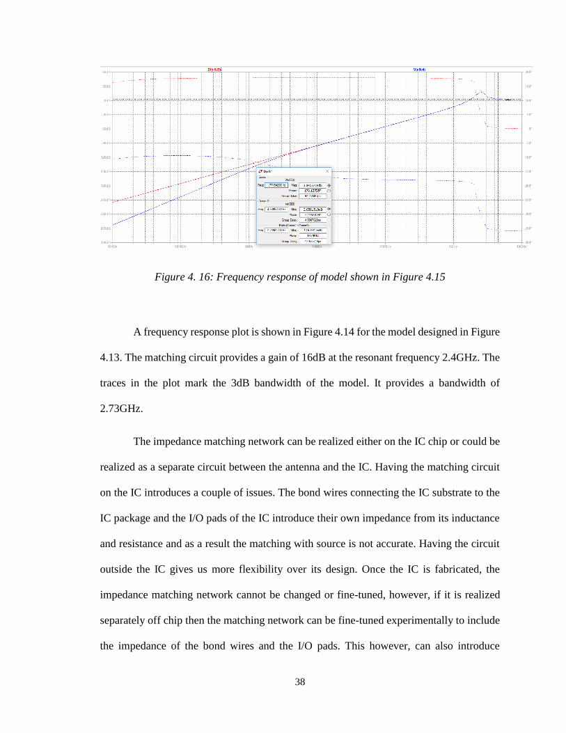
Figure 4. 16: Frequency response of model shown in Figure 4.15
A frequency response plot is shown in Figure 4.14 for the model designed in Figure
4.13. The matching circuit provides a gain of 16dB at the resonant frequency 2.4GHz. The
traces in the plot mark the 3dB bandwidth of the model. It provides a bandwidth of
2.73GHz.
The impedance matching network can be realized either on the IC chip or could be
realized as a separate circuit between the antenna and the IC. Having the matching circuit
on the IC introduces a couple of issues. The bond wires connecting the IC substrate to the
IC package and the I/O pads of the IC introduce their own impedance from its inductance
and resistance and as a result the matching with source is not accurate. Having the circuit
outside the IC gives us more flexibility over its design. Once the IC is fabricated, the
impedance matching network cannot be changed or fine-tuned, however, if it is realized
separately off chip then the matching network can be fine-tuned experimentally to include
the impedance of the bond wires and the I/O pads. This however, can also introduce
39
tolerance issues and the traces to external components introduce their own impedance
which is difficult to model. Both approaches have some advantages and disadvantages.
However, the size of the inductors used in the matching circuit is larger than most of the
highest valued inductors offered by 8RF process. The inds inductor model offered by the
8RF process can offer inductance values as high as 70nH. But to achieve the high
inductance value, the number of turns of the inductor coil are increased and this introduces
a high turn-to-turn parasitic capacitance. As a result, it is decided to design a matching
circuit off-chip.
40
CHAPTER 5
AMPLIFIER DESIGN
The amplifier circuit of the RF energy harvesting device is designed using 130nm
CMOS technology. A cascaded voltage doubler circuit must be designed using diode
connected NMOS and capacitors. The goal is to achieve an output voltage of up to 4V,
which is enough to charge Enerchip solid-state batteries [29].
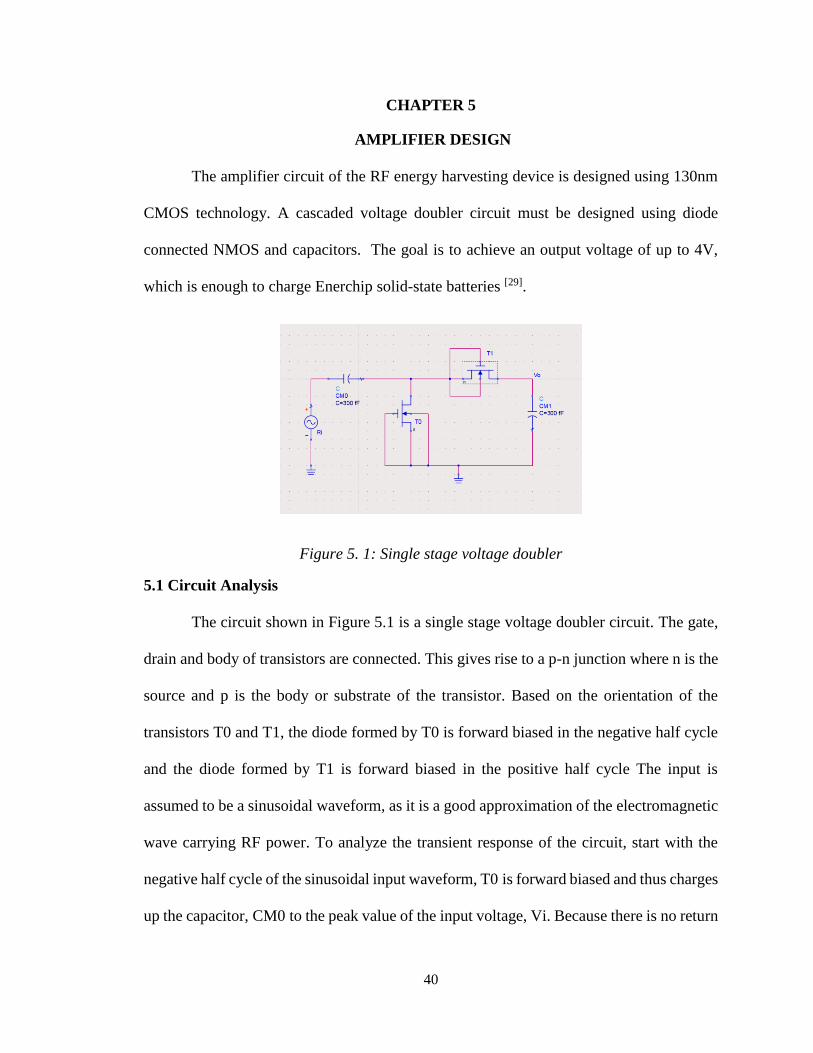
Figure 5. 1: Single stage voltage doubler
5.1 Circuit Analysis
The circuit shown in Figure 5.1 is a single stage voltage doubler circuit. The gate,
drain and body of transistors are connected. This gives rise to a p-n junction where n is the
source and p is the body or substrate of the transistor. Based on the orientation of the
transistors T0 and T1, the diode formed by T0 is forward biased in the negative half cycle
and the diode formed by T1 is forward biased in the positive half cycle The input is
assumed to be a sinusoidal waveform, as it is a good approximation of the electromagnetic
wave carrying RF power. To analyze the transient response of the circuit, start with the
negative half cycle of the sinusoidal input waveform, T0 is forward biased and thus charges
up the capacitor, CM0 to the peak value of the input voltage, Vi. Because there is no return
41
path for capacitor CM0 to discharge into, it remains fully charged. At the same time,
T1 conducts via T0 charging up capacitor, CM1. During the positive half cycle, T0 is
reverse biased blocking the discharging of CM0 while diode T1 is forward biased charging
up capacitor CM1 and providing a path for capacitor CM0 to discharge. But because there
is a voltage across capacitor CM0 already equal to the peak input voltage,
capacitor CM1 charges to twice the peak voltage value of the input signal. The voltage
across capacitor CM1 is the output voltage Vo. However, in practical applications the
capacitor CM1 never charges up to twice the input voltage due to the voltage drops across
T0 and T1. Figure 5.2 shows the simulation results of a single stage voltage doubler. The
output voltage increases by 45% over the input voltage.
5.1.1 Output voltage analysis
To achieve high efficiency and maximum possible output voltage it is necessary to
analyze the circuit shown in figure 5.1 in detail and figure out the factors affecting the
output voltage Vo. The output voltage Vo is given by the following equation 5.1 [16] and
the threshold voltage Vth is given in equation 5.2 [28].
𝑉𝑜 = 2(𝑅𝑖 − 𝑉𝑡ℎ) (Eq. 5.1)
Vo = Output Voltage, Ri = Input voltage, Vth = Threshold voltage of NMOS
𝑉𝑡ℎ = 𝑉𝑡ℎ0 + ϒ(√|2𝜙 + 𝑉𝑆𝐵| − √|2𝜙|) (Eq. 5.2)
Vth0 = Threshold voltage when VSB is 0, ϕ = Fermi potential, VSB = Source-body voltage
42
It can be seen from equation 5.1 that one way to maximize the output voltage would be to
minimize the threshold voltage of the transistors. Equation 5.2 shows that threshold voltage
is increased with an increase in the voltage VSB between source and body. In the design
presented above, gate and source are tied to the same potential and hence VSB is zero. Thus,
the threshold voltage is minimized.
5.1.2 Output current analysis
It is important to know the current through the NMOS. This helps us determine the
output power of the circuit. The drain current of the NMOS transistor is derived by Neamen
D. in [27]. The current 𝐼𝐷 for NMOS in the linear region is given by equation 5.3 [27]and the
current in the saturation region is given by equation 5.4 [27].
𝐼𝐷 =𝑘′
2
𝑊
𝐿[2(𝑉𝐺𝑆 − 𝑉𝑡ℎ)𝑉𝐷𝑆 − 𝑉𝐷𝑆
2] (Eq. 5.3)
𝐼𝐷 =𝑘′
2
𝑊
𝐿(𝑉𝐺𝑆 − 𝑉𝑡ℎ)2
(Eq. 5.4)
W = Width of the NMOS, L = Length of the NMOS
VGS = Gate to Source voltage, VDS = Drain to source voltage
Equation 5.4 gives the current voltage relationship assuming a constant channel length L.
However, when the device is operated in saturation region, the channel length L is not
constant. This is because when the NMOS is operating in saturation region, the depletion
region near the drain extends laterally into the channel, thus reducing the channel length.
Now the width of the depletion region depends on VDS and therefore the effective channel
length also depends on VDS. This is known as channel length modulation effect. Equation
43
5.5 describes the current voltage relationship after incorporating the effects of channel
length modulation.
𝐼𝐷 =𝑘′
2
𝑊
𝐿(𝑉𝐺𝑆 − 𝑉𝑡ℎ)2(1 + 𝜆𝑉𝐷𝑆)
(Eq. 5.5)
The parameter λ is called the channel length modulation parameter. The effect of
channel length modulation is more prominent in processes where minimum gate length is
below 1µm. This is because the reduction in channel length in saturation region of
operation is a significant fraction of the original channel length L. The reduction in channel
length gives rise to some undesirable effects like the hot electron effect. As the electric
field in the drain junction space charge region increases, electron hole pairs are generated
by impact ionization. The generated electrons are swept to the drain and the generated holes
are swept towards the substrate. Some electrons get attracted to the oxide because of their
high energies [27]. This is concerning for thin gate oxides because thin oxides make it
easier for the high energy electrons to overcome the potential barrier of the oxide.
Sometimes the electrons get trapped in the gate oxide building up the negative charging
effect. This increases the threshold voltage of the NMOS. These high energy electrons are
known as hot electrons, hence the name hot electron effect. This accumulation of electrons
is a continuous process and builds up over time. This causes the device to degrade and
deviate from their original properties.
For the diode connected NMOS used in this design, the transistors operate in
saturation region. Hence the current is given by equation 5.5. The amount of current 𝐼𝐷
depends directly on the Width to Length ratio of the transistor. Therefore, we should select
a transistor with high W/L ratio. This increases the amount of current through the
44
transistors and eventually helps in increasing the output current. This helps increase the
output power. However, increasing the W/L ratio means the transistor will have more width
and the space charge depletion region is bigger. This amount of hot electrons generated is
more and thus the probability of the electrons getting trapped in the gate oxide increases.
We use a low threshold NMOS with thin gate oxide. Therefore, we should strike a balance
in deciding the W/L ratio. Higher ratio gives us more current but also increases the chances
of device degradation. Increasing the W/L ratio also increases the gate oxide capacitance.
This is because the capacitance between two plates is directly proportional to area of the
plates. Increasing W/L increases the gate width and thus the overall area. This increase in
capacitance slows down the device and introduces delays in voltage amplification.
5.2 8RF technology
The 8RF CMOS technology offers various options of NMOS transistors. Various
options available for transistors and capacitors were studied. We need a MOSFET with low
threshold voltage and high current. The Low Vth option provides the lowest threshold
voltage. So, the Low Vth MOSFET is selected for the design.
5.3 Simulation
The input RF signal is approximated using a sine wave input of given frequency.
Initial simulations are done for 915MHz and 2.4GHz separately but it was found that the
output voltage and current does not show significant change with the change in frequency.
So, all the simulation results shown below are for an input frequency of 915MHz. The input
45
voltage discussed from here on refers to peak amplitude of the sine wave. To decide the
input voltage, various factors are considered. Initially the various values of incident input
voltage are calculated for various values of input power. The values of input power are
decided based on the RF power survey. For example, the peak power observed in SLO was
around -30dBm which corresponds to 1µW. Table 5.1 shows the result of these
calculations. The formula given in equation 5.6 is used to calculate the input voltage. The
value of the input impedance Z is calculated in section 4.4.
𝑉 = √𝑃𝑍 (Eq. 5.6)
Table 5. 1: Input power vs input voltage relationship
Input power (dBm) Input power (µW) Input voltage (mV)
-30 1 131
-26 2.5 208
-22 6.3 331
-18 15.8 524
-14 39.8 830
-12 63.1 1046
The literature survey carried out on similar RF energy harvesting circuits revealed
Karolak D. et al. in [16] use an input voltage between 300-500mV for testing their amplifier
circuit. The threshold voltage of the transistor used is also considered. Based on this, the
input voltage is decided to be 500mV for design purposes. This corresponds to an input
power of around -20dBm. The voltage levels for incident power up to -25dBm are less than
the Vth of the transistors. Once the circuit is deigned, it will be tested for various input
voltages and the corresponding output voltages will be determined. This will help
determine the least amount of power that can be used to generate a voltage of up to 4V.
46
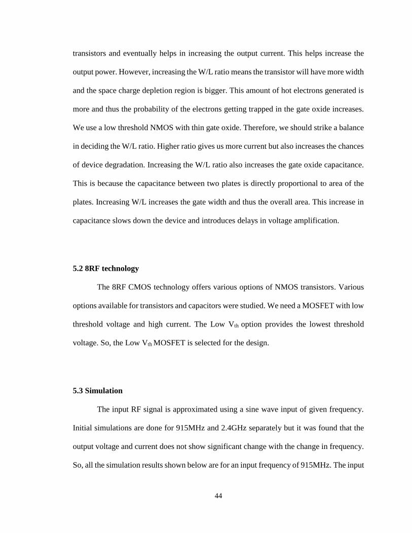
The number of voltage doubler stages simulated are increased gradually to study
the effect of number of stages on output voltage. An optimum number of stages should be
determined based on the output voltage requirements, power requirements and area
constraints. The initial W/L ratio is set to R4. The capacitor value is decided to be 300fF.
Low value of capacitance allows the circuit to reach peak output voltage quickly. The
transient response of a single stage voltage doubler is shown in figure 5.2. The thick lines
representing Ri is because a 915MHz sinewave for a duration of 100 micro seconds is
shrunk to fit the image. The peak output voltage is 725mV. The output current measured
at the terminal of capacitor CM1 is 36µA. There is a ripple at the output of about 60mV.
Figure 5. 2: Transient response of single stage voltage doubler
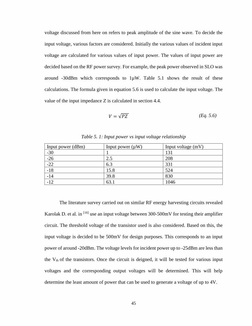
The output voltage increased by 45% for a single stage voltage doubler. A two-
stage voltage doubler is simulated under similar conditions. Figure 5.3 shows the schematic
of the two-stage voltage doubler.
47
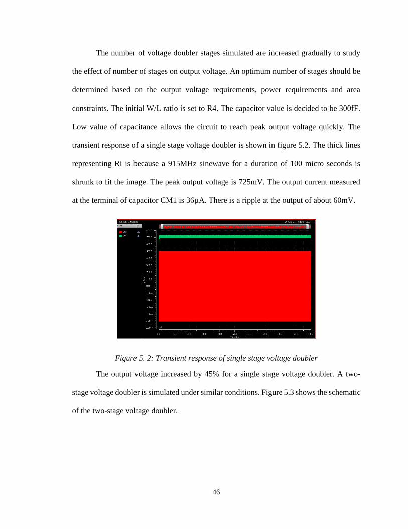
Figure 5. 3: Two stage voltage doubler
The transient response of the two-stage voltage doubler is shown in figure 5.4. The
output of first stage is also shown on the plot under the name ‘net9’. The peak output
voltage is 1.215V. The ripple in the output voltages increases to 100mV.
Figure 5. 4: Transient response of two stage voltage doubler
A four-stage voltage doubler shown in Figure 5.5 is simulated under above
mentioned conditions. Its transient response is shown in Figure 5.6. The peak output
voltage is 1.5098 V. It is important to note that the size of the output ripple increases with
48
the number of stages. The output of first stage is shown under ‘net9’ and the output of
second stage is shown under ‘net14’.
Figure 5. 5: Four stage voltage doubler
Figure 5. 6 Transient response of four stage voltage doubler
An eight-stage voltage doubler shown in Figure 5.7 is simulated similar conditions
as for previous simulations. Its transient response is shown in Figure 5.8. The peak output
voltage is 1.4595 V. The output voltage after 8 stages is less than the output voltage after
4 stages. It is important to note that the size of the output ripple is 400mV peak to peak.
49
Figure 5. 7: Eight stage voltage doubler
Figure 5. 8: Transient response of eight stage voltage doubler
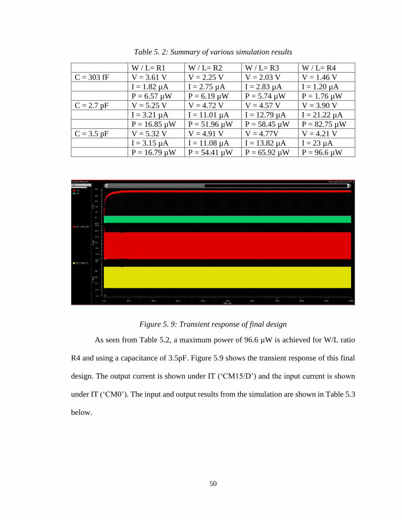
The eight-stage doubler is simulated a few times varying some key parameters like
the W/L ratio and the value of CM0 and CM1. It is observed from the simulations that a
higher value of capacitance can provide better amplification. Increasing the capacitance for
the same W/L ratio exhibits a sharp increase in output voltage. The results of this variation
are summarized in Table 5.2. The values of current and voltage are the peak values
observed and the value for power is the maximum instantaneous power obtained at the
output.
50
Table 5. 2: Summary of various simulation results
W / L= R1 W / L= R2 W / L= R3 W / L= R4
C = 303 fF V = 3.61 V V = 2.25 V V = 2.03 V V = 1.46 V
I = 1.82 µA I = 2.75 µA I = 2.83 µA I = 1.20 µA
P = 6.57 µW P = 6.19 µW P = 5.74 µW P = 1.76 µW
C = 2.7 pF V = 5.25 V V = 4.72 V V = 4.57 V V = 3.90 V
I = 3.21 µA I = 11.01 µA I = 12.79 µA I = 21.22 µA
P = 16.85 µW P = 51.96 µW P = 58.45 µW P = 82.75 µW
C = 3.5 pF V = 5.32 V V = 4.91 V V = 4.77V V = 4.21 V
I = 3.15 µA I = 11.08 µA I = 13.82 µA I = 23 µA
P = 16.79 µW P = 54.41 µW P = 65.92 µW P = 96.6 µW
Figure 5. 9: Transient response of final design
As seen from Table 5.2, a maximum power of 96.6 µW is achieved for W/L ratio
R4 and using a capacitance of 3.5pF. Figure 5.9 shows the transient response of this final
design. The output current is shown under IT (‘CM15/D’) and the input current is shown
under IT (‘CM0’). The input and output results from the simulation are shown in Table 5.3
below.
51
Table 5. 3: Input-Output results from the simulations of amplifier
Parameter Input Output
Ipeak 676 µA 23 µA
Irms 478 µA 16 µA
Vpeak 500mV 4.2V
Vrms 353mV 4.082V
Pmax 338 µW 96.6 µW
Prms 168 µW 93.91 µW
Efficiency(rms/peak) 55.66%/28.57%
The final design is simulated for different input voltage levels. The results of the
simulations are shown in Table 5.4. This helps us determine the least amount of input
voltage required to meet the minimum requirements of output voltage. We can then
determine the least amount of input power required to meet the output voltage
requirements. The least amount of voltage required to achieve the minimum output voltage
requirements of 4.0V is 480mV. This corresponds to an input power of -18dBm.
Table 5. 4: Output voltages resulting from given input voltage levels
Input voltage (mV) Output voltage (V)
300 2.2
400 3.2
480 4.0
500 4.2
600 5.2
700 6.1
5.4 Layout
What makes IC technology so promising is the size of the transistors. For the 8RF
technology the channel length of the transistors can be as small as 130nm. Layout design
is all about efficiently connecting all the transistors in the schematic on a physical level to
minimize delays, reduce parasitics and optimize performance. We need obtain maximum
52
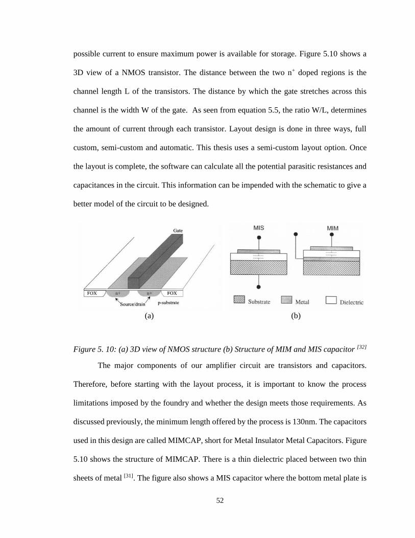
possible current to ensure maximum power is available for storage. Figure 5.10 shows a
3D view of a NMOS transistor. The distance between the two n+ doped regions is the
channel length L of the transistors. The distance by which the gate stretches across this
channel is the width W of the gate. As seen from equation 5.5, the ratio W/L, determines
the amount of current through each transistor. Layout design is done in three ways, full
custom, semi-custom and automatic. This thesis uses a semi-custom layout option. Once
the layout is complete, the software can calculate all the potential parasitic resistances and
capacitances in the circuit. This information can be impended with the schematic to give a
better model of the circuit to be designed.
(a) (b)
Figure 5. 10: (a) 3D view of NMOS structure (b) Structure of MIM and MIS capacitor [32]
The major components of our amplifier circuit are transistors and capacitors.
Therefore, before starting with the layout process, it is important to know the process
limitations imposed by the foundry and whether the design meets those requirements. As
discussed previously, the minimum length offered by the process is 130nm. The capacitors
used in this design are called MIMCAP, short for Metal Insulator Metal Capacitors. Figure
5.10 shows the structure of MIMCAP. There is a thin dielectric placed between two thin
sheets of metal [31]. The figure also shows a MIS capacitor where the bottom metal plate is
53
reduced by a doped substrate. The MIM aspect ratio cannot be larger than 3:1. Our design
has an aspect ratio of 4:3, so it is well within the requirements. The capacitance per area
information is given by the fabricator and the size of capacitors is calculated for the
required capacitance.
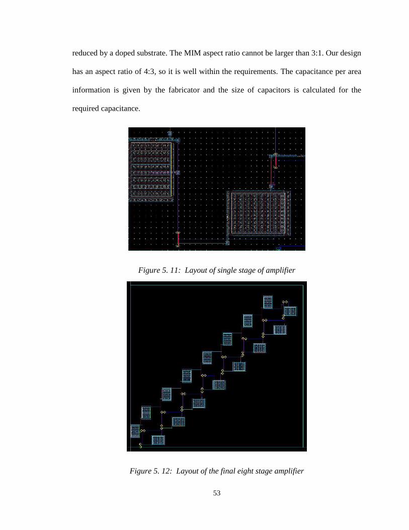
Figure 5. 11: Layout of single stage of amplifier
Figure 5. 12: Layout of the final eight stage amplifier
54
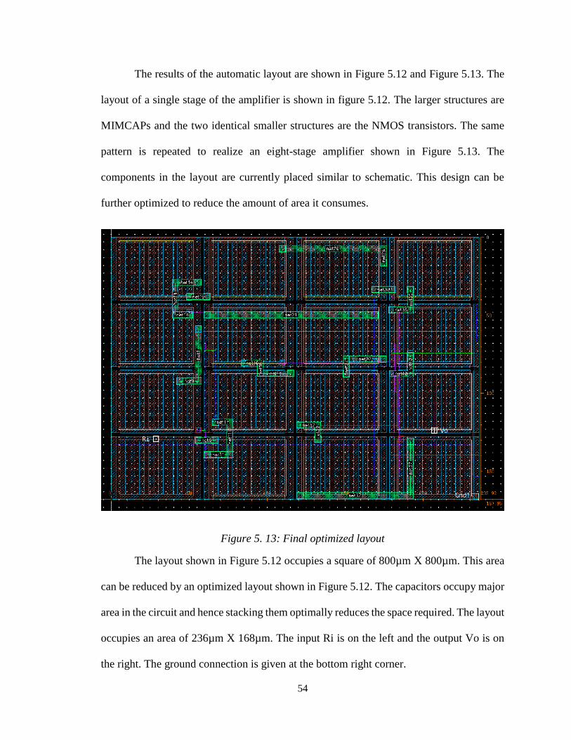
The results of the automatic layout are shown in Figure 5.12 and Figure 5.13. The
layout of a single stage of the amplifier is shown in figure 5.12. The larger structures are
MIMCAPs and the two identical smaller structures are the NMOS transistors. The same
pattern is repeated to realize an eight-stage amplifier shown in Figure 5.13. The
components in the layout are currently placed similar to schematic. This design can be
further optimized to reduce the amount of area it consumes.
Figure 5. 13: Final optimized layout
The layout shown in Figure 5.12 occupies a square of 800µm X 800µm. This area
can be reduced by an optimized layout shown in Figure 5.12. The capacitors occupy major
area in the circuit and hence stacking them optimally reduces the space required. The layout
occupies an area of 236µm X 168µm. The input Ri is on the left and the output Vo is on
the right. The ground connection is given at the bottom right corner.
55
5.5 Applications
The harvested power can be stored in a solid-state battery as discussed in section
2.4. The output voltage of our final design is 4.2V at peak and the output current is 23 µA
at peak. This fulfills the basic requirement to charge Enerchip CBC005 model of the battery
shown in Figure 2.7. The device could also be used to charge CBC050 battery model, but
due to its higher capacity, it would take longer time to charge the CBC050 compared to the
CBC005 model. It should be noted however, that there is a ripple at the output voltage of
the amplifier which could potentially decrease the life of the battery [29].
The energy harvesting device can also be integrated directly with an application
instead of charging a battery. However, with ambient power harvesting, the availability of
power is not certain all the time. Due to that reason it would be better to have a battery
backup available. Table 5.5 lists a variety of low voltage, low power requirement
applications. Each circuit has its own input voltage requirement. The designed RF energy
harvesting device can be integrated with the listed applications with a DC-DC converter
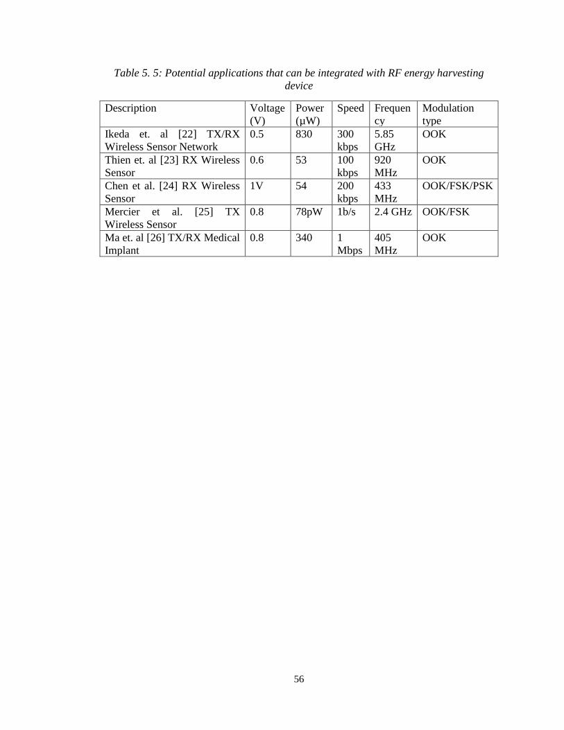
block in between. Ikeda et. al [22] have proposed Wireless Sensor Network node that
operates on 0.5V and consumes 830 µW at a data rate of 300kbps. If the node is adjusted
for lower data rates, it consumes less power. Ma et. al [26] propose a medical implant that
operates at 0.8 V and consumes only 340 µW of power at 1Mbps data rate.
56
Table 5. 5: Potential applications that can be integrated with RF energy harvesting
device
Description Voltage
(V)
Power
(µW)
Speed Frequen
cy
Modulation
type
Ikeda et. al [22] TX/RX
Wireless Sensor Network
0.5 830 300
kbps
5.85
GHz
OOK
Thien et. al [23] RX Wireless
Sensor
0.6 53 100
kbps
920
MHz
OOK
Chen et al. [24] RX Wireless
Sensor
1V 54 200
kbps
433
MHz
OOK/FSK/PSK
Mercier et al. [25] TX
Wireless Sensor
0.8 78pW 1b/s 2.4 GHz OOK/FSK
Ma et. al [26] TX/RX Medical
Implant
0.8 340 1
Mbps
405
MHz
OOK
57
CHAPTER 6
CONCLUSION
This thesis presents design of an RF energy harvesting device that consists of an
antenna, matching circuit and an amplifier chip. Two antenna designs are proposed in this
thesis, one for 915 MHz and one for 2.4 GHz. The antenna dimensions are 100 mm X 79.18
mm and 38 mm X 30.75mm respectively. Either of the two antennas can be selected
depending upon the size constraints and frequency band for energy harvesting. According
to the survey of RF power in San Luis Obispo, the peak ambient power available between
2.3 GHz-2.5 GHz is between -20 to -30dBm, which corresponds to a range of 1 µW – 10
µW. However, the amplifier requires a minimum of -18dBm to generate an output voltage
high enough to charge the Enerchip battery. This would require slightly higher power than
the observed power levels. The ambient power available between 800-1000MHz is below
-40dBm which is too little for the amplifier to generate the desired output. Hence given the
choices, a 2.4GHz antenna is best suited for San Luis Obispo. If a manual transmitter is
used to supply the power, then either antenna can be used. Also, if a different battery or
application is used which requires input voltage less than 4V, the amplifier can be used at
the observed power levels. The relationship between input and output voltage is given in
Table 5.4. Table 6.1 provides a summary of the design.
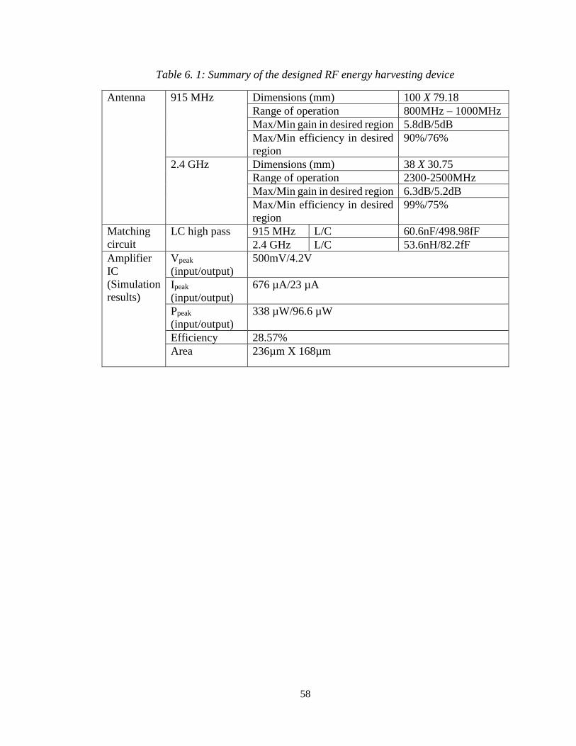
58
Table 6. 1: Summary of the designed RF energy harvesting device
Antenna 915 MHz Dimensions (mm) 100 X 79.18
Range of operation 800MHz – 1000MHz
Max/Min gain in desired region 5.8dB/5dB
Max/Min efficiency in desired
region
90%/76%
2.4 GHz Dimensions (mm) 38 X 30.75
Range of operation 2300-2500MHz
Max/Min gain in desired region 6.3dB/5.2dB
Max/Min efficiency in desired
region
99%/75%
Matching
circuit
LC high pass 915 MHz L/C 60.6nF/498.98fF
2.4 GHz L/C 53.6nH/82.2fF
Amplifier
IC
(Simulation
results)
Vpeak
(input/output)
500mV/4.2V
Ipeak
(input/output)
676 µA/23 µA
Ppeak
(input/output)
338 µW/96.6 µW
Efficiency 28.57%
Area 236µm X 168µm
59
CHAPTER 7
FUTURE WORK
7.1 Voltage regulator
The output of the amplifier shows a ripple of similar frequency as the input
frequency. This fluctuation in voltage is undesired by many applications. It can also make
it difficult to charge the battery properly. A DC-DC voltage converter or a rectifier circuit
can help stabilize the output of the device and make it more reliable. A different topology
for the amplifier circuit can be tried as well. Salter et al. [38] use a switch capacitor DC-DC
converter as their amplifier circuit. This provides a DC voltage across load.
7.2 Verification of design
The design of the amplifier circuit has been simulated successfully. However, the
circuit was simulated without any information regarding the parasitic capacitances and
resistances. The layout of the design can be used to generate an extracted view of the
schematic with all parasitic information. ADS and Cadence have a link that can be used to
test the antenna, matching circuit and the amplifier circuit all together. The entire system
needs to be simulated before fabrication. The antenna needs to be tested in an anechoic
chamber to experimentally determine the antenna gain vs frequency. The next step would
be to get the chip fabricated and test it under various input conditions. The total input
impedance can be experimentally determined, and the matching circuit can be changed
accordingly. This would give a better transfer of input power from antenna to amplifier
circuit.
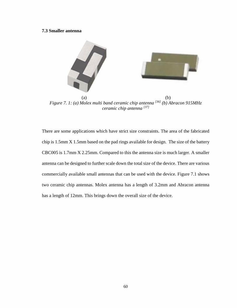
60
7.3 Smaller antenna
(a) (b)
Figure 7. 1: (a) Molex multi band ceramic chip antenna [36] (b) Abracon 915MHz
ceramic chip antenna [37]
There are some applications which have strict size constraints. The area of the fabricated
chip is 1.5mm X 1.5mm based on the pad rings available for design. The size of the battery
CBC005 is 1.7mm X 2.25mm. Compared to this the antenna size is much larger. A smaller
antenna can be designed to further scale down the total size of the device. There are various
commercially available small antennas that can be used with the device. Figure 7.1 shows
two ceramic chip antennas. Molex antenna has a length of 3.2mm and Abracon antenna
has a length of 12mm. This brings down the overall size of the device.
61
REFERENCES
[1] T. Itoh, "Ultra low power wireless sensor nodes for expanding application of the
Internet of Things," 2016 IEEE CPMT Symposium Japan (ICSJ), Kyoto, 2016, pp.
74-75. doi: 10.1109/ICSJ.2016.7801319
[2] Y. Liang, X. Meng, Y. Hu and K. Zhang, "Design and implementation of an ultra-
low power wireless sensor network for indoor environment monitoring," 2017
IEEE 17th International Conference on Communication Technology (ICCT),
Chengdu, 2017, pp. 937-940. doi: 10.1109/ICCT.2017.8359772
[3] Zhihua Wang, Xiaoyu Zhang, Xinkai Chen, Lingwei Zhang and Hanjun Jiang, "An
energy-efficient ASIC with real-time work-on-demand for wireless body sensor
network," 2008 IEEE International Conference on Electron Devices and Solid-
State Circuits, Hong Kong, 2008, pp. 1-6. doi: 10.1109/EDSSC.2008.4760681
[4] Texas Instruments, ‘The Evolution of Internet of Things”, White Paper, 2013.
[5] Minh-Thien Hoang, Nobuyuki Sugii, Koichiro Ishibashi, “A 1.36μW 312–315MHz
synchronized-OOK receiver for wireless sensor networks using 65nm SOTB
CMOS technology” Solid-State Electronics, Volume 117, 2016, pp. 161-169. doi:
10.1016/ISSN 0038-1101
[6] Federal Communications Commission, “FCC Table of Frequency Allocation”
.Available: https://transition.fcc.gov/oet/spectrum/table/fcctable.pdf
[7] Balanis, Constantine A. Antenna Theory, Analysis and Design. Third ed. Hoboken,
NJ: John Wiley & Sons, 2005.
62
[8] A. S. Andrenko, Xianyang Lin and Miaowang Zeng, "Outdoor RF spectral survey:
A roadmap for ambient RF energy harvesting," TENCON 2015 - 2015 IEEE Region
10 Conference, Macao, 2015, pp. 1-4. doi: 10.1109/TENCON.2015.7373140
[9] J. C. Kwan and A. O. Fapojuwo, "Measurement and Analysis of Available Ambient
Radio Frequency Energy for Wireless Energy Harvesting," 2016 IEEE 84th
Vehicular Technology Conference (VTC-Fall), Montreal, QC, 2016, pp. 1-6. doi:
10.1109/VTCFall.2016.7881084
[10] T. Beng Lim, N. M. Lee and B. K. Poh, "Feasibility study on ambient RF energy
harvesting for wireless sensor network," 2013 IEEE MTT-S International
Microwave Workshop Series on RF and Wireless Technologies for Biomedical and
Healthcare Applications (IMWS-BIO), Singapore, 2013, pp. 1-3. doi:
10.1109/IMWS-BIO.2013.6756226
[11] X. Lu, P. Wang, D. Niyato, D. I. Kim and Z. Han, "Wireless Networks With RF
Energy Harvesting: A Contemporary Survey," in IEEE Communications Surveys
& Tutorials, vol. 17, no. 2, pp. 757-789, Secondquarter 2015. doi:
10.1109/COMST.2014.2368999
[12] Powercast, “TX91501 – 915 MHz Powercaster TM Transmitter”. Available:
http://www.powercastco.com/products/powercaster-transmitter/
[13] FCC code of regulations 47CFR Part 15. Available:
https://www.law.cornell.edu/cfr/text/47/part-15
[14] J. W. Zhang et al., "Wireless energy harvesting using serially connected voltage
doublers," 2010 Asia-Pacific Microwave Conference, Yokohama, 2010, pp. 41-44.
63
[15] P. Nintanavongsa, U. Muncuk, D. R. Lewis and K. R. Chowdhury, "Design
Optimization and Implementation for RF Energy Harvesting Circuits," in IEEE
Journal on Emerging and Selected Topics in Circuits and Systems, vol. 2, no. 1, pp.
24-33, March 2012. doi: 10.1109/JETCAS.2012.2187106
[16] D. Karolak, T. Taris, Y. Deval, J. Béguéret and A. Mariano, "Design comparison
of low-power rectifiers dedicated to RF energy harvesting," 2012 19th IEEE
International Conference on Electronics, Circuits, and Systems (ICECS 2012),
Seville, 2012, pp. 524-527. doi: 10.1109/ICECS.2012.6463693
[17] FCC, “Cellular Market Areas Map”. Available:
https://www.fcc.gov/sites/default/files/wireless/auctions/data/maps/CMA.pdf
[18] FCC, “Chart of Licenses”. Available:
https://wireless2.fcc.gov/UlsEntry/attachments/attachmentViewRD.jsp?applType
=search&fileKey=1382746707&attachmentKey=18830422&attachmentInd=appl
Attach
[19] Cellular communication transmission towers in San Luis Obispo, CA. Available:
http://www.cellreception.com/towers/towers.php?city=SAN+LUIS+OBISPO&sta
te_abr=ca
[20] N. Abdullah, A. M. Shire, E. Mohd and A. M. Shire, "Rectenna for RF energy
harvesting," 2016 International Conference on Advances in Electrical, Electronic
and Systems Engineering (ICAEES), Putrajaya, 2016, pp. 318-321. doi:
10.1109/ICAEES.2016.7888061
[21] Rogers et al. Radio Frequency Integrated Circuit Design. First ed. Norwood, MA:
Artech House, Inc. 2003.
64
[22] S. Ikeda et al., "A 0.5-V 5.8-GHz low-power asymmetrical QPSK/OOK transceiver
for wireless sensor network," The 20th Asia and South Pacific Design Automation
Conference, Chiba, 2015, pp. 40-41. doi: 10.1109/ASPDAC.2015.7058976
[23] H. M. Thien, N. Sugii and K. Ishibashi, "A 53µW −82dBm sensitivity 920MHz
OOK receiver design using bias switch technique on 65nm SOTB CMOS
technology," 2014 SOI-3D-Subthreshold Microelectronics Technology Unified
Conference (S3S), Millbrae, CA, 2014, pp. 1-2. doi: 10.1109/S3S.2014.7028185
[24] S. Chen and K. Cheng, "A 433 MHz 54 µW OOK/FSK/PSK compatible wake-up
receiver with 11 µW low-power mode based on injection-locked
oscillator," ESSCIRC Conference 2016: 42nd European Solid-State Circuits
Conference, Lausanne, 2016, pp. 137-140. doi: 10.1109/ESSCIRC.2016.7598261
[25] P. P. Mercier, S. Bandyopadhyay, A. C. Lysaght, K. M. Stankovic and A. P.
Chandrakasan, "A 78 pW 1 b/s 2.4 GHz radio transmitter for near-zero-power
sensing applications," 2013 Proceedings of the ESSCIRC (ESSCIRC), Bucharest,
2013, pp. 133-136. doi: 10.1109/ESSCIRC.2013.6649090
[26] C. Ma, C. Hu, J. Cheng, L. Xia and P. Y. Chiang, "A Near-Threshold, 0.16 nJ/b
OOK-Transmitter With 0.18 nJ/b Noise-Cancelling Super-Regenerative Receiver
for the Medical Implant Communications Service," in IEEE Transactions on
Biomedical Circuits and Systems, vol. 7, no. 6, pp. 841-850, Dec. 2013. doi:
10.1109/TBCAS.2013.2253555
[27] Neamen Donald A. Solid State Electronics. Fourth ed. New York, NY: McGraw
Hill, 2012.
65
[28] D. Al-Shebanee, R. Wunderlich and S. Heinen, "Design of highly sensitive CMOS
RF energy harvester using ultra-low power charge pump," 2015 IEEE Wireless
Power Transfer Conference (WPTC), Boulder, CO, 2015, pp. 1-4. doi:
10.1109/WPT.2015.7140163
[29] Cymbet Corporation, “Enerchip Bare Die Rechargeable Solid-State Batteries
Datasheet”. Available: http://www.cymbet.com/pdfs/DS-72-41%20v6.pdf
[30] T. Le, K. Mayaram and T. Fiez, "Efficient Far-Field Radio Frequency Energy
Harvesting for Passively Powered Sensor Networks," in IEEE Journal of Solid-
State Circuits, vol. 43, no. 5, pp. 1287-1302, May 2008. doi:
10.1109/JSSC.2008.920318
[31] B. Landgraf, "Capacitors in heterogeneous IC systems-Consequences on compact
modeling," 2014 Proceedings of the 21st International Conference Mixed Design
of Integrated Circuits and Systems (MIXDES), Lublin, 2014, pp. 62-65. doi:
10.1109/MIXDES.2014.6872154
[32] Baker Jacob R. CMOS circuit design, layout, and simulation. Third ed. Piscataway,
NJ: IEEE press, 2010.
[33] ITO, “Radio Spectrum Management in China”. Available:
https://www.itu.int/en/ITU-D/Regional-
Presence/AsiaPacific/Documents/Events/2017/Sep-SECB/Presentations/D1-2-
Kan%20Runtian-
Radio%20Spectrum%20Management%20Strategies%20in%20China.pdf
66
[34] Singapore Spectrum Allocation Chart. Available: https://www.imda.gov.sg/-
/media/imda/files/regulation-licensing-and-consultations/frameworks-and-
policies/spectrum-management-and-coordination/spectrumchart.pdf?la=en
[35] Radio Spectrum Allocations, Canada. Available: https://www.ic.gc.ca/eic/site/smt-
gst.nsf/vwapj/spectallocation-08.pdf/$FILE/spectallocation-08.pdf
[36] Molex, “Ceramic Chip Antenna Datasheet” Available:
https://www.mouser.com/datasheet/2/276/2030070001_ANTENNAS-
1218567.pdf
[37] Abracon, “Ceramic Chip Antenna Datasheet” Available:
https://www.mouser.com/datasheet/2/3/ACAG1204-915-T-1314113.pdf
[38] T. Salter, K. Choi, M. Peckerar, G. Metze and N. Goldsman, "RF energy
scavenging system utilising switched capacitor DC-DC converter," in Electronics
Letters, vol. 45, no. 7, pp. 374-376, 26 March 2009. doi: 10.1049/el.2009.0153