Embed Size (px)
Citation preview
Prof. Paolo Colantonioa.a. 2011‐12

Analogue ElectronicsProf. Paolo Colantonio 2 | 37
• As for the FET, we can use a load line
V [V]CE
I [mA]C
0
10
20
30
40
50
60
70
VCC
V /CC RC
ICQ
VCEQ
Q
Static load line
Dynamic load line
R //C RL
ic
t
vce
t

Analogue ElectronicsProf. Paolo Colantonio 3 | 37
• As for the FET, there are several forbidden regions

Analogue ElectronicsProf. Paolo Colantonio 4 | 37
• Clipping of a sinusoidal signal

Analogue ElectronicsProf. Paolo Colantonio 5 | 37
VCC
RE
C1
vout
vin R2
R1
RinRin’
• In the classical CC configuration, the biasing network reduces the amplifier inputresistance
1in ie fe ER h h R
1 2' / / / /in in inR R R R R

Analogue ElectronicsProf. Paolo Colantonio 6 | 37
• The adoption of a different configuration allows to increase the input resistancepresented to the input signal source
1 2 3' / / / /in inR R R R R
VCC
RE
C1
vout
vin
R2
R1
RinRin’
C’R3
• Assuming for the moment C’=0 (i.e. opencircuit), the input impedance is increased
R1
vout
1/hoehfeibhie
vin
RE
ib
R2
R3
Rin’
• However R3 is travelled by the base current, thus it cannot be too high (max. n105)• The presence of C’ solve the problem

Analogue ElectronicsProf. Paolo Colantonio 7 | 37
• The dynamic circuit becomes the following
RE vout
vinR2
R1
RinRin’
R3
• The dynamic circuit becomes the following
REvout
vin
Rin
R3
R1 R2
1 2' / / / /E ER R R R
• Applying the Miller theorem, the resistor R3 is equivalent to input and outputresistances (very high, accounting for AV1) given by
33, 1in
V
RRA
3, 3 1
Vout
V
AR RA
31 ' / / 1 '1in fe E fe E
V
RR h R h RA

Analogue ElectronicsProf. Paolo Colantonio 8 | 37
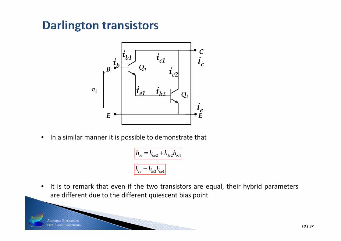
• An useful combination of two (or more) transistors is the Darlington connection
• The current gain of the first transistor is multiplied by that of the second to producea combination that acts like a single transistor with an hfe equal to the product ofthe gains of the two transistors.

Analogue ElectronicsProf. Paolo Colantonio 9 | 37
vi Q2
B Q1
E E
C
ibib1 ic1
ie1 ib2
ic2
ic
ie
• (vc=0)
1 2 1 1 2 2 1 2 2 1 2 11c c c fe b fe b fe b fe e fe fe fe bi i i h i h i h i h i h h h i
1 2 1 1 21cfe fe fe fe fe fe
b
i h h h h h hi
1 1 2 2 1 1 2 1 2 11 1i ie b ie b fe b fe ie b ie ie fe bv h i h i h i h h i h h h i
1 2 1 1 2 11iie ie fe ie ie fe ie
b
v h h h h h h hi
Analogue ElectronicsProf. Paolo Colantonio 10 | 37
vi Q2
B Q1
E E
C
ibib1 ic1
ie1 ib2
ic2
ic
ie
• In a similar manner it is possible to demonstrate that
2 2 1oe oe fe oeh h h h
2 1re ie oeh h h
• It is to remark that even if the two transistors are equal, their hybrid parametersare different due to the different quiescent bias point

Analogue ElectronicsProf. Paolo Colantonio 11 | 37
• Gives a better representation at high frequencies
• The bandwidth of the deviceis given by f
' ' ' ' '
1 12 2b e b c b e b e b e
fC C r C r
• The transition frequency fT (atwhich the gain drops to 1) isgiven by
0T fef h f

Analogue ElectronicsProf. Paolo Colantonio 12 | 37
A bipolar transistor as a constant current source
• The resistors R1 and R2 form a potential divider that applies a constant voltage to thebase of the transistor.
• The constancy of VBE results in a fixed emitter voltage which results in a constantemitter (and thus collector) current
• The circuit may be refined by using a Zener diode in place of R2 to improve theconstancy of the emitter voltage
2
1 2B CC
RV VR R
E B BE BV V V V
2
1 2
1BE CC
E E
V RI V constR R R R

Analogue ElectronicsProf. Paolo Colantonio 13 | 37
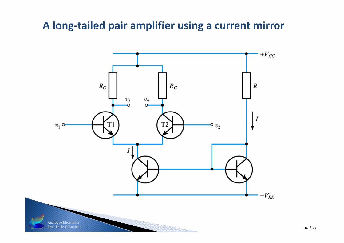
A bipolar transistor as a current mirror
CC BE CCV V VIR R
• Transistor T1 and T2 have the same VBE• thus the same IB• thus the same IC

Analogue ElectronicsProf. Paolo Colantonio 14 | 37
A bipolar transistor as a differential amplifier
• If RE is very high (theoretically an infinite value) the CMRR is very high

Analogue ElectronicsProf. Paolo Colantonio 15 | 37
• The superposition principle can be applied
VCC
2Re
Rc
vo
+-
vs
Rs
E
-VEE
Rc
vo
+-
vs / 2
Rs
E
b)Rc
vo
+-
vs / 2
Rs
E
b)a) a) Equivalent circuit for the evaluation of the common mode voltage gain AC
b) Equivalent circuit for the evaluation of the differential mode voltage gain Ad
Analogue ElectronicsProf. Paolo Colantonio 16 | 37
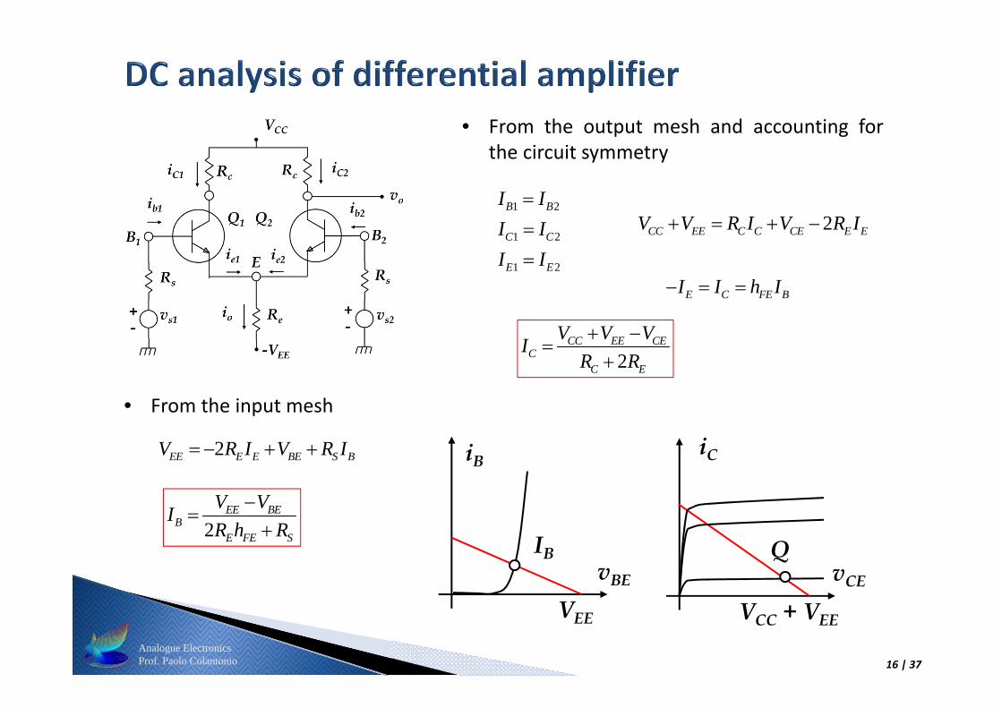
• From the output mesh and accounting forthe circuit symmetry
2CC EE C C CE E EV V R I V R I 1 2
1 2
1 2
B B
C C
E E
I II II I
E C FE BI I h I
2CC EE CE
CC E
V V VIR R
• From the input mesh
2EE E E BE S BV R I V R I
2EE BE
BE FE S
V VIR h R
iB
vBE
IB
VEE
iC
vCE
Q
VCC + VEE
Analogue ElectronicsProf. Paolo Colantonio 17 | 37
1 2s s sv v v
1 2C feo
cs S ie fe E
R hvAv R h h R
1 2 2s
s svv v
12
C feod
s S ie
R hvAv R h
1 212
S ie fe Ed
c S ie
R h h RACMRRA R h
• CMRR high requires larger RE,
thus complicating the biasing
Analogue ElectronicsProf. Paolo Colantonio 18 | 37
Analogue ElectronicsProf. Paolo Colantonio 19 | 37
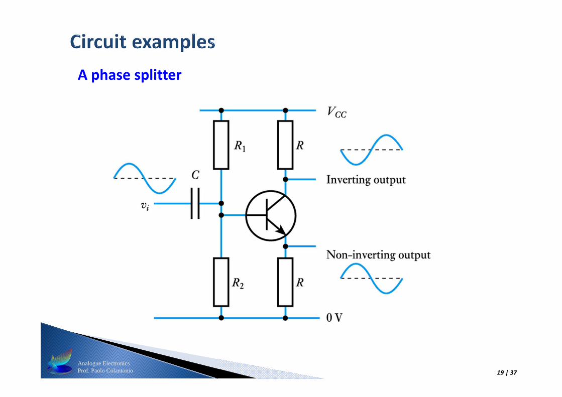
A phase splitter

Analogue ElectronicsProf. Paolo Colantonio 20 | 37
A voltage regulator
o Z BEV V v const
Analogue ElectronicsProf. Paolo Colantonio 21 | 37
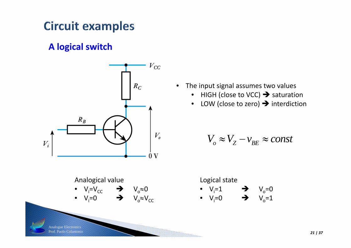
A logical switch
o Z BEV V v const
• The input signal assumes two values• HIGH (close to VCC) saturation• LOW (close to zero) interdiction
Analogical value• Vi=VCC Vo0• Vi=0 VoVCC
Logical state• Vi=1 Vo=0• Vi=0 Vo=1

Analogue ElectronicsProf. Paolo Colantonio 22 | 37
• The hybrid ‐model gives a better representation at high frequencies for the BJT
• At medium frequency the hybrid ‐model and the hybrid model should beequivalent

Analogue ElectronicsProf. Paolo Colantonio 23 | 37
' ' '
' '' ' '
' '
' ' ' ' ' ' '
' ' '
1
/ /
1 1
Cm
T
feC m b e m b e b fe b b e
m
b c b e rere b c b e re b e
ce b e b c re
ie bb b e b c bb b e bb ie b e
cc ccC m re ce ce m re
c b c b e ce b c
IgV
hI g v g r I h I r
g
V r hh r r h rV r r h
h r r r r r r h r
V VI g h V V g hI r r r r
gm
rb’e
rb’c
rbb’
gce

Analogue ElectronicsProf. Paolo Colantonio 24 | 37
IC VCE T
gm n10 mA/V
rbb’ n102
rb’e n103
Cb’e (Ce) n102 pF
Cb’c (Cc) n pF
hfe n100
hie n103
Legend• means increases• means decreases• means is stable

Analogue ElectronicsProf. Paolo Colantonio 25 | 37
• The direct methods requires to evaluate the amplifier transfer function
svsvsG
i
o
20GsG
• The cut‐off frequency are found by solving the equation
• Being G0 the medium frequency amplifier gain• Obviously, the approach is rigorous, but not even simple…
• Two simplified methods are typically adopted• The poles method• The method of time constant in open or short circuit

Analogue ElectronicsProf. Paolo Colantonio 26 | 37
• If the capacitance present in the circuit are not interacting, thus for each capacitorCX is computed the time constant
X X XR C • Being RX the equivalent resistor seen by CX
• The low cut‐off frequency is given by:
22
1
1N
Ln n
• The high cut‐off frequency is given by:2
21
1 N
nnH
The bandwidth is approximated in excess

Analogue ElectronicsProf. Paolo Colantonio 27 | 37
• If the capacitance present in the circuit are interacting, then the following approachis adopted
• The low cut‐off frequency is given by:1 ,
1N
Ln n sc
• The high cut‐off frequency is given by: ,1
1 N
n ocnH
• Being
• n,sc the time constant associated to the capacitance Cn, assuming all theother capacitance as short circuit
• n,oc the time constant associated to the capacitance Cn, assuming all theother capacitance as open circuit
The bandwidth is approximated in defect

Analogue ElectronicsProf. Paolo Colantonio 28 | 37
fL fHpoles method poles method
s.c. or o.c. time constant method

Analogue ElectronicsProf. Paolo Colantonio 29 | 37
• Capacitive coupling between amplifier stages
• A two‐stage DC‐coupled amplifier
Analogue ElectronicsProf. Paolo Colantonio 30 | 37
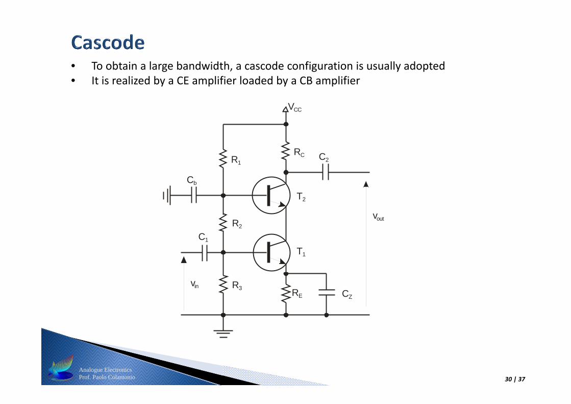
• To obtain a large bandwidth, a cascode configuration is usually adopted• It is realized by a CE amplifier loaded by a CB amplifier
VCC
RE
C1
vout
vin
R2
R1RC
Cb
R3CZ
C2
T1
T2

Analogue ElectronicsProf. Paolo Colantonio 31 | 37
• The AC circuit becomes the following
vo u t
vin
RC
R =RB 1//R2
T1
T2
• For the analysis at medium frequency, starting from the CB amplifier:
,2 ,2 ,2,2
,2 ,2 ,2 ,2
fe b C fe CoutV
i b ie ie
h i R h RvAv i h h
vout
hfe,2ib,2
hie,2vi2 RCib,2
Ri2
,2 ,2 ,22
,2,2,2 ,2 ,2 ,2 11 1
ie b ieii
fefe b fe b
h i hvRhh i h i

Analogue ElectronicsProf. Paolo Colantonio 32 | 37
• The CE now can be analysed referring to the following scheme
,2
,2,1 ,2 ,1
,2 ,2 ,2
,1 ,1 ,1 ,1
fefe C
fe i bV i ieout
Vi b ie b ie
hh Rh R i
A v hvAv i h i h
,2
C
ie
R
h,2
,1ie
fe
hh
,21 feh,1
,1 ,1
feC
ie ie
hR
h h
,1,1
ini ie
b
vR hi
hfe ,1 i b ,1hie ,1vin
ib ,1
R3//R2 A vv,2 i,2
+
-Ri,2 vo u tRC
vi,2
• The cascode performances at the medium frequency are practically coincident with the CE performances
o CR R

Analogue ElectronicsProf. Paolo Colantonio 33 | 37
• For the analysis of the bandwidth, we can analyse what is the behaviour of a CE and CB separately, by using the hybrid model
CE
• For the determination of the high frequency limitation, applying the methods of time constant it follows
,1 ,1 ,1 'e e S e bbC R C r
gm,1vb’e,1
rb’e,1R //R3 2 RC vo,1
Cc,1
Ce,1
rbb’,1
vb’e,1
gm,1vb’e,1
rb’e,1R //R3 2 RC vo,1Ce,1
rbb’,1
vb’e,1
gm,1vb’e,1
rb’e,1R //R3 2 RC vo,1
Cc,1rbb’,1
vb’e,1
,1 ,1 ,1 ,11c c S m C C c CC R g R R C R
' 2 3 ' '/ / / / / /S bb s b e bbR r R R R r r
,1S m S CV I R I g R I R

Analogue ElectronicsProf. Paolo Colantonio 34 | 37
,1 ,1 'e e bbC r
,1 ,1c c CC R
• The high cut‐off frequency of a CE is given by
,1 ,1
1H
e c
freq1/c,1 1/e ,1
R h /hc fe ,1 ie ,1
|A |V
• To have a large gain, a big value of RC is required, which however reduces the bandwidth
• The adoption of the CB as loading impedance, allows to reach the same voltage gain (as previously saw) but presenting to the CE stage an equivalent resistance (RC) much lower

Analogue ElectronicsProf. Paolo Colantonio 35 | 37
• Assuming now the CE loaded by the CB, with an input resistance very low
vo u t
vin
RC
R =RB 1//R2
T1
T2
,1 ,1 ,1 'e e S e bbC R C r ,1 ,1 ,1 'c c S c bbC R C r
freq1/c,1 1/e ,1
R h /hc fe ,1 ie ,1
|A |V

Analogue ElectronicsProf. Paolo Colantonio 36 | 37
CB
• For the determination of the high frequency limitation, applying the methods of time constant it follows
,2,2
,2
ee
m
Cg
,2 ,2c c CC R
' ,2
' ,2,2 ' ,2
',2
,2,2
',2
1 11
b e
b em b e
bb
mm
bb
V vv
I g vr
VI gg
r
,2 ' ,2
' ,2 ,2 ' ,2 ' ,2 ' ,2 0m b e C
b e m b e b e b e
C
V I g v R
v g v r vV RI
gm,2vb’e,2
rb’e,2
RCCc,2
Ce,2
rbb’,2
vb’e,2
Rout,CE
gm,2vb’e,2
rb’e,2
RC
V
rbb’,2
vb’e,2
Rout,CE
+-
I
gm,2vb’e,2
rb’e,2
RC
rbb’,2
vb’e,2
Rout,CE V +-
I

Analogue ElectronicsProf. Paolo Colantonio 37 | 37
,1 ,1 'c c bbC r ,2,2
,2
ee
m
Cg
,2 ,2c c CC R
• The cascode high cut‐off frequency is given by
,1 ,1 'e e bbC r
freq1/c ,1 1/e ,1
R h /hc fe ,1 ie ,1
|A |V
1/c ,21/c ,2