Embed Size (px)
Citation preview

Embedded Box T K S - P 2 0 - C V 0 1
TKS-P20-CV01
Fanless Embedded Box
Intel® Atom™ N2600 1.6 GHz Processor
1 GbE LAN, 5 USB2.0, 2 COM
1 VGA, 1 HDMI, 1 Mini Card or mSATA
TKS-P20-CV01 Manual 1st Ed.
July 2013

Embedded Box T K S - P 2 0 - C V 0 1
i
Copyright Notice
This document is copyrighted, 2013. All rights are reserved. The
original manufacturer reserves the right to make improvements to
the products described in this manual at any time without notice.
No part of this manual may be reproduced, copied, translated, or
transmitted in any form or by any means without the prior written
permission of the original manufacturer. Information provided in
this manual is intended to be accurate and reliable. However, the
original manufacturer assumes no responsibility for its use, or for
any infringements upon the rights of third parties that may result
from its use.
The material in this document is for product information only and is
subject to change without notice. While reasonable efforts have
been made in the preparation of this document to assure its
accuracy, AAEON assumes no liabilities resulting from errors or
omissions in this document, or from the use of the information
contained herein.
AAEON reserves the right to make changes in the product design
without notice to its users.

Embedded Box T K S - P 2 0 - C V 0 1
ii
Acknowledgments All other products’ name or trademarks are properties of their respective owners.
AMI is a trademark of American Megatrends Inc.
CompactFlash™ is a trademark of the Compact Flash Association.
Microsoft Windows® is a registered trademark of Microsoft
Corp.
Intel®, Atom™ are trademarks of Intel Corporation.
PC/AT, PS/2, and VGA are trademarks of International Business Machines Corporation.
All other product names or trademarks are properties of their respective owners.

Embedded Box T K S - P 2 0 - C V 0 1
iii
Packing List
Before you begin operating your PC, please make sure that the
following materials are enclosed:
1 TKS-P20-CV01 Embedded Controller
1 DVD-ROM for manual (in PDF format) and drivers
If any of these items should be missing or damaged, please contact
your distributor or sales representative immediately.

Embedded Box T K S - P 2 0 - C V 0 1
iv
Safety & Warranty 1. Read these safety instructions carefully.
2. Keep this user's manual for later reference.
3. Disconnect this equipment from any AC outlet before cleaning. Do not use liquid or spray detergents for cleaning. Use a damp cloth.
4. For pluggable equipment, the power outlet must be installed near the equipment and must be easily accessible.
5. Keep this equipment away from humidity.
6. Put this equipment on a firm surface during installation. Dropping it or letting it fall could cause damage.
7. The openings on the enclosure are for air convection. Protect the equipment from overheating. DO NOT COVER THE OPENINGS.
8. Make sure the voltage of the power source is correct before connecting the equipment to the power outlet.
9. Position the power cord so that people cannot step on it. Do not place anything over the power cord.
10. All cautions and warnings on the equipment should be noted.
11. If the equipment is not used for a long time, disconnect it from the power source to avoid damage by transient over-voltage.
12. Never pour any liquid into an opening. This could cause fire or electrical shock.
13. Never open the equipment. For safety reasons, only qualified service personnel should open the equipment.
14. If any of the following situations arises, get the equipment checked by service personnel:
a. The power cord or plug is damaged.
b. Liquid has penetrated into the equipment.
c. The equipment has been exposed to moisture.
Embedded Box T K S - P 2 0 - C V 0 1
v
d. The equipment does not work well, or you cannot get it to work according to the user’s manual.
e. The equipment has been dropped and damaged.
f. The equipment has obvious signs of breakage.
15. DO NOT LEAVE THIS EQUIPMENT IN AN ENVIRONMENT WHERE THE STORAGE TEMPERATURE IS BELOW -20°C (-4°F) OR ABOVE 55°C (131°F). IT MAY DAMAGE THE EQUIPMENT.
FCC
This device complies with Part 15 FCC Rules.
Operation is subject to the following two
conditions: (1) this device may not cause
harmful interference, and (2) this device must
accept any interference received including
interference that may cause undesired
operation.
Caution: There is a danger of explosion if the battery is incorrectly replaced. Replace only with the same or equivalent type recommended by the manufacturer. Dispose of used batteries according to the manufacturer’s instructions and your local government’s recycling or disposal directives.

Embedded Box T K S - P 2 0 - C V 0 1
vi
Below Table for China RoHS Requirements 产品中有毒有害物质或元素名称及含量
AAEON Boxer/ Industrial System
有毒有害物质或元素
部件名称 铅
(Pb)
汞
(Hg)
镉
(Cd)
六价铬
(Cr(VI))
多溴联苯
(PBB)
多溴二苯醚
(PBDE)
印刷电路板
及其电子组件 × ○ ○ ○ ○ ○
外部信号
连接器及线材 × ○ ○ ○ ○ ○
外壳 × ○ ○ ○ ○ ○
中央处理器
与内存 × ○ ○ ○ ○ ○
硬盘 × ○ ○ ○ ○ ○
电源 × ○ ○ ○ ○ ○
O:表示该有毒有害物质在该部件所有均质材料中的含量均在 SJ/T 11363-2006 标准规定的限量要求以下。
X:表示该有毒有害物质至少在该部件的某一均质材料中的含量超出
SJ/T 11363-2006 标准规定的限量要求。 备注: 一、此产品所标示之环保使用期限,系指在一般正常使用状况下。 二、上述部件物质中央处理器、内存、硬盘、电源为选购品。
Embedded Box T K S - P 2 0 - C V 0 1
vii
Contents
Chapter 1 General Information
1.1 Introduction................................................................ 1-2
1.2 Features .................................................................... 1-3
1.3 Specifications ............................................................ 1-4
Chapter 2 Hardware Installation
2.1 Safety Precautions .................................................... 2-2
2.2 Mechanical Drawing of TKS-P20-CV01.................... 2-3
2.3 A Quick Tour of the TKS-P20-CV01 ......................... 2-4
2.4 Installing mSATA and RAM module.......................... 2-8
2.5 List of Jumpers .......................................................... 2-9
2.6 List of Connector ....................................................... 2-9
2.7 Setting Jumpers ........................................................ 2-10
2.8 COM2 Pin8 Function Selection (JP1) ....................... 2-11
2.9 Clear CMOS Selection (JP2) .................................... 2-11
2.10 AT/ATX Power Supply Mode Selection (JP6)......... 2-11
2.11 COM Port 1 Connector (CN1) ................................. 2-12
2.12 COM Port 2 Connector (CN2) ................................. 2-12
2.13 DIO Connector (CN3).............................................. 2-14
2.14 +5V Output for SATA HDD Connector (CN4) ......... 2-15
2.15 LPC Port Connector (CN10) ................................... 2-15
2.16 USB2.0 Port 1 ~ 5 Connector.................................. 2-16

Embedded Box T K S - P 2 0 - C V 0 1
viii
2.17 VGA Port Connector (CN12)................................... 2-17
2.18 HDMI Type C Connector (CN17) ............................ 2-18
2.19 Mini Card Slot (PCIE1)............................................ 2-19
Chapter 3 AMI BIOS Setup
3.1 System Test and Initialization. .................................. 3-2
3.2 AMI BIOS Setup ........................................................ 3-3
Chapter 4 Driver Installation
4.1 Installation ................................................................. 4-3
Appendix A Programming The Watchdog Timer
A.1 Watchdog Timer Registers .................................A-2
A.2 WatchDog Sample Program..................................A-3
Appendix B I/O Information
B.1 I/O Address Map....................................................B-2
B.2 Memory Address Map............................................B-4
B.3 IRQ Mapping Chart ................................................B-5
B.4 DMA Channel Assignments...................................B-7
Appendix C Mating Connector
C.1 List of Mating Connectors and Cables.................. C-2
Appendix D AHCI Setting
D.1 Setting AHCI ......................................................... D-2
Appendix E Digital I/O Ports
E.1 Electrical Specifications for Digital I/O Ports .........E-2

Embedded Box T K S - P 2 0 - C V 0 1
ix
E.2 DIO Programming..................................................E-2
E.3 Digital I/O Register.................................................E-3
E.4 Digital I/O Sample Program ...................................E-4
Embedded Box T K S - P 2 0 - C V 0 1
Chapter 1 General Information 1- 1
General
Chapter
1Information

Embedded Box T K S - P 2 0 - C V 0 1
Chapter 1 General Information 1- 2
1.1 Introduction
The newest EmBox series TKS-P20-CV01 has been introduced by
AAEON and it utilizes Intel® Atom™ processor. In this era of
information explosion, the advertising of consumer products will not
be confined to the family television, but will also spread to
high-traffic public areas, like department stores, the bus,
transportation station, the supermarket etc. The advertising
marketing industry will resort to every conceivable means to
transmit product information to consumers. System integrators will
need a multifunction device to satisfy commercial needs for such
public advertising.
The TKS-P20-CV01 is designed for indoor environments due to the
following reasons; first, the TKS-P20-CV01 offers low power
consumption system that while operating in ambient temperatures
ranging from 0° to 55°C. The TKS-P20-CV01 is a standalone high
performance controller designed for long-life operation and with
high reliability. It can replace traditional methods and become the
mainstream controller for the multimedia entertainment market.

Embedded Box T K S - P 2 0 - C V 0 1
Chapter 1 General Information 1- 3
1.2 Features
Intel® Atom™ N2600 Processor up to 1.6GHz
SODIMM DDR3 800MHz Memory up to 2 GB
DIN RAIL and Fanless system
Mini HDMI and VGA Support
Gigabit Ethernet LAN x 1
USB2.0 x 5, COM x 2, 4-bits Digital I/O
mSATA or Mini Card (Half size) x 1
DC IN +12 or +7~30V Wide Range DC Input Optional

Embedded Box T K S - P 2 0 - C V 0 1
Chapter 1 General Information 1- 4
1.3 Specifications
CPU Onboard Intel® Atom™ N2600 Processor up to 1.6 GHz
Chipset Intel® Atom™ N2600 + NM10
System Memory 204-pin DDR3 SODIMM x 1, Max. 2GB
VGA D-SUB 15 x 1 Display
Interface HDMI HDMI type C (Mini HDMI) x 1
SSD mSATA x 1 (Half-size) Storage
Device HDD Optional by request
LAN Gigabit Ethernet Network
Wireless Optional by Mini Card
USB Host USB 2.0 x 2
LAN RJ-45 x 1
Serial Port RS-232 x 1, RS-232/422/485 x 1 Front I/O
Others System & HDD indicator LED x 2, Power Switch, DC-in
DIO DIO 4-bit with VCC and ground in Rear I/O
Audio Mic-in/ Line-out
Bottom I/O USB Host USB2.0 x 3
Expansion Mini PCIe Mini Card half size (or mSATA)
Indicator Front Power LED x 1, HDD LED x 1
Power Requirement DC-in +12V ATX or DC-in +7~30V ATX (Optional)
Power Consumption Intel® Atom™ N2600 1.6 GHz, DDR3 800 2GB, 1.5A @ +12V

Embedded Box T K S - P 2 0 - C V 0 1
Chapter 1 General Information 1- 5
System Cooling Fanless
Mounting Wallmount, DIN RAIL (optional)
Dimension 4.7" x 2.3" x 4.3" (120mm x 59.5mm x110mm)
Gross Weight 2.2 lb (1 Kg)
Net Weight 1.8 lb (0.82 Kg)
Operating Temperature 32°F ~ 131°F (0°C ~ 55°C)
Storage Temperature -40°F ~ 176°F (-40°C ~ 80°C)
Operating Humidity 0%~90% relative humidity, non-condensing
Anti-Vibration 2 g rms/ 5 ~ 500Hz/ operation (mSATA)
Anti-Shock 20 G peak acceleration (11 msec. duration) (mSATA)
Certification EMC CE/FCC Class A
OS Support Windows® XP Embedded, Windows® XP, Windows® 7, Linux Fedora
Note: COM1 and COM2’s performance will be among 9,600 to 115,200
bps depend on the system loadings.

Embedded Box T K S - P 2 0 - C V 0 1
Chapter 2 Quick Installation Guide 2-1
Quick Installation
Chapter
2Guide

Embedded Box T K S - P 2 0 - C V 0 1
Chapter 2 Quick Installation Guide 2-2
2.1 Safety Precautions
Always completely disconnect the power cord from your board whenever you are working on it. Do not make connections while the power is on, because a sudden rush of power can damage sensitive electronic components. Always ground yourself to remove any static charge before touching the board. Modern electronic devices are very sensitive to static electric charges. Use a grounding wrist strap at all times. Place all electronic components on a static-dissipative surface or in a static-shielded bag when they are not in the chassis

Embedded Box T K S - P 2 0 - C V 0 1
Chapter 2 Quick Installation Guide 2-3
2.2 Mechanical Drawing of TKS-P20-CV01
Figure 2.1 Mechanical Drawing of TKS-P20-CV01
Dimension: 120mmx 59.5mmx 110mm

Embedded Box T K S - P 2 0 - C V 0 1
Chapter 2 Quick Installation Guide 2-4
2.3 A Quick Tour of the TKS-P20-CV01
Before you start to set up the TKS-P20-CV01, take a moment to
become familiar with the locations and purposes of the controls, drives,
connections and ports, which are illustrated in the figures below.
When you place the TKS-P20-CV01 upright on the desktop, its front
panel appears as Show in Figure 2-1.
Front View
Front View of the Point of Care Terminal
(1)
(8)
(6)
(7)
(2)
(3)
(4)
(5)
(1). Power and HDD indicator LED
(2). Gigabit Ethernet LAN Port
(3). VGA port
(4). USB x2
(5). Mini HDMI port

Embedded Box T K S - P 2 0 - C V 0 1
Chapter 2 Quick Installation Guide 2-5
(6). COM1 & COM2
(7). Power Switch
(8). Power DC-IN
Remark: Power DC-IN with +12V or option wide range power board for
7-30V DC input
Top Side View
Top side View of the TKS-P20-CV01
(9)
(10)
(9). 4 bit Digital IO with VCC and ground pin
(10). Audio port with Mic-in & line-out

Embedded Box T K S - P 2 0 - C V 0 1
Chapter 2 Quick Installation Guide 2-6
UBottom View
Top side View of the TKS-P20-CV01
(11)
(11). USB x3
Rear side View
Rear side View of the TKS-P20-CV01
(13)
(12)
Embedded Box T K S - P 2 0 - C V 0 1
Chapter 2 Quick Installation Guide 2-7
(12). DIN RAIL kit (optional)
(13). Wall mount Kit (optional)
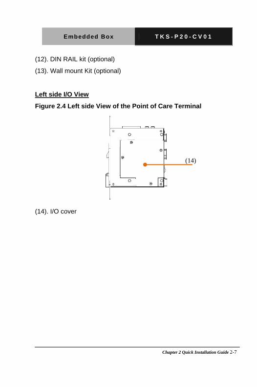
Left side I/O View
Figure 2.4 Left side View of the Point of Care Terminal
(14)
(14). I/O cover

Embedded Box T K S - P 2 0 - C V 0 1
Chapter 2 Quick Installation Guide 2-8
2.4 Installing mSATA and RAM module
Step 1: Unfasten the screws on the I/O cover from Left side
Step 2: Remove the I/O cover then you can see the inside of system
Step 3: Locate the memory module, Insert the gold colored contact into the Memory Socket. Push the module down, until it is firmly seated locking two latches on the sides.
Step 4: Locate the mSATA module(same with mini card module), insert the gold colored contact into the Socket of mSATA mini card. Push the module down, until it is firmly seated by locking two latches on the sides.
Step 5: Please take the I/O cover back to the chassis. Then fasten the 4 screws of I/O cover.
RAM Module
mSATA

Embedded Box T K S - P 2 0 - C V 0 1
Chapter 2 Quick Installation Guide 2-9
2.5 List of Jumpers
The board has a number of jumpers that allow you to configure your system to suit your application.
The table below shows the function of each of the board's jumpers:
Label Function
JP1 COM2 RI/+5/+12V Selection
JP2 Clear CMOS
JP6 AT/ATX Power Mode Selection
2.6 List of Connectors
The board has a number of connectors that allow you to configure your system to suit your application. The table below shows the function of each board's connectors:
Label Function
CN1 COM Port 1
CN2 COM Port 2
CN3 Digital I/O
CN4 +5V Output for SATA HDD
CN5 SATA Port
CN7 RJ-45 Ethernet
CN10 LPC Expansion I/F
CN11 USB Port 5
CN12 Analog CRT Display
CN13 USB Port 3
CN14 USB Port 4
CN16 USB Port 1 and 2

Embedded Box T K S - P 2 0 - C V 0 1
Chapter 2 Quick Installation Guide 2-10
CN17 HDMI Type C
PCIE1 Mini Card
2.7 Setting Jumpers
You configure your card to match the needs of your application by
setting jumpers. A jumper is the simplest kind of electric switch. It
consists of two metal pins and a small metal clip (often protected by a
plastic cover) that slides over the pins to connect them. To “close” a
jumper you connect the pins with the clip.
To “open” a jumper you remove the clip. Sometimes a jumper will have
three pins, labeled 1, 2 and 3. In this case you would connect either
pins 1 and 2 or 2 and 3.
1 2 3
Open Closed Closed 2-3
A pair of needle-nose pliers may be helpful when working with jumpers.
If you have any doubts about the best hardware configuration for your
application, contact your local distributor or sales representative before
you make any change.
Generally, you simply need a standard cable to make most
connections.

Embedded Box T K S - P 2 0 - C V 0 1
Chapter 2 Quick Installation Guide 2-11
2.8 COM2 Pin8 Function Selection (JP1)
+12V Ring +5V
JP1 Function
1-2 +12V
3-4 Ring (Default)
5-6 +5V
2.9 Clear CMOS Selection (JP2)
1 2 3
1 2 3
Normal Clear CMOS
JP2 Function
1-2 Normal (Default)
2-3 Clear CMOS
2.10 AT/ATX Power Supply Mode Selection (JP6)
1 2 3
1 2 3
AT Mode ATX Mode
JP6 Function
1-2 AT Mode
2-3 ATX Mod (Default)

Embedded Box T K S - P 2 0 - C V 0 1
Chapter 2 Quick Installation Guide 2-12
2.11 COM Port 1 Connector (CN)
Pin Pin Name Signal Type Signal Level
1 DCD1 IN
2 RX1 IN
3 TX1 OUT ±9V
4 DTR1 OUT ±9V
5 GND GND
6 DSR1 IN
7 RTS1 OUT ±9V
8 CTS1 IN
9 RI1 IN
2.12 COM Port 2 Connector (CN2)

Embedded Box T K S - P 2 0 - C V 0 1
Chapter 2 Quick Installation Guide 2-13
RS-232
Pin Pin Name Signal Type Signal Level
1 DCD2 IN
2 RX2 IN
3 TX2 OUT ±9V
4 DTR2 OUT ±9V
5 GND GND
6 DSR2 IN
7 RTS2 OUT ±9V
8 CTS2 IN
9 RI2/+5V/+12V IN/ PWR +5V/+12V
RS-422
Pin Pin Name Signal Type Signal Level
1 RS422_TX- OUT ±5V
2 RS422_TX+ OUT
3 RS422_RX+ IN ±5V
4 RS422_RX- IN
5 NC
6 NC
7 NC
8 NC/+5V/+12V PWR +5V/+12V
9 GND GND
Embedded Box T K S - P 2 0 - C V 0 1
Chapter 2 Quick Installation Guide 2-14
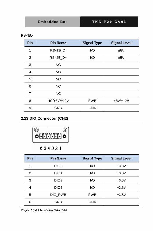
RS-485
Pin Pin Name Signal Type Signal Level
1 RS485_D- I/O ±5V
2 RS485_D+ I/O ±5V
3 NC
4 NC
5 NC
6 NC
7 NC
8 NC/+5V/+12V PWR +5V/+12V
9 GND GND
2.13 DIO Connector (CN2)
Pin Pin Name Signal Type Signal Level
1 DIO0 I/O +3.3V
2 DIO1 I/O +3.3V
3 DIO2 I/O +3.3V
4 DIO3 I/O +3.3V
5 DIO_PWR PWR +3.3V
6 GND GND

Embedded Box T K S - P 2 0 - C V 0 1
Chapter 2 Quick Installation Guide 2-15
Access Address based on SIO
LDN6 GPIO Port Location
(Pin #) Input Output
GPIO1 2 Reg 0xD2, bit 0 Reg 0xD1, bit 0
GPIO2 3 Reg 0xD2, bit 1 Reg 0xD1, bit 1
GPIO3 4 Reg 0xD2, bit 2 Reg 0xD1, bit 2
GPIO4 5 Reg 0xD2, bit 3 Reg 0xD1, bit 3
2.14 +5V Output for SATA HDD Connector (CN4)
+5V
GND
Pin Pin Name Signal Type Signal Level
1 +5V PWR +5V
2 GND GND
2.15 LPC Port Connector (CN10)
LAD0 1
12
LAD1LAD2LAD3
LFRAME#LRESET#
LDRQ0LDRQ1
SERIRQ
GNDLCLK
+3.3V

Embedded Box T K S - P 2 0 - C V 0 1
Chapter 2 Quick Installation Guide 2-16
Pin Pin Name Signal Type Signal Level
1 LAD0 I/O +3.3V
2 LAD1 I/O +3.3V
3 LAD2 I/O +3.3V
4 LAD3 I/O +3.3V
5 +3.3V PWR +3.3V
6 LFRAME# IN
7 LRESET# OUT +3.3V
8 GND GND
9 LCLK OUT
10 LDRQ0 IN
11 LDRQ1 IN
12 SERIRQ I/O +3.3V
2.16 USB2.0 Port 1 ~ 5 Connector
Pin Pin Name Signal Type Signal Level
1 +5V PWR +5V
2 USB5_D- DIFF
3 USB5_D+ DIFF
4 GND GND

Embedded Box T K S - P 2 0 - C V 0 1
Chapter 2 Quick Installation Guide 2-17
2.17 VGA Port Connector (CN12)
Pin Pin Name Signal Type Signal Level
1 RED OUT
2 GREEN OUT
3 BLUE OUT
4 NC
5 GND GND
6 RED_GND_RTN GND
7 GREEN_GND_RTN GND
8 BLUE_GND_RTN GND
9 +5V PWR +5V
10 GND GND
11 NC
12 DDC_DATA I/O +5V
13 HSYNC OUT
14 VSYNC OUT
15 DDC_CLK I/O +5V

Embedded Box T K S - P 2 0 - C V 0 1
Chapter 2 Quick Installation Guide 2-18
2.18 HDMI Type C Connector (CN17)
Pin Pin Name Signal Type Signal Level
1 GND GND
2 HDMI_TX2+ DIFF
3 HDMI_TX2- DIFF
4 GND GND
5 HDMI_TX1+ DIFF
6 HDMI_TX1- DIFF
7 GND GND
8 HDMI_TX0+ DIFF
9 HDMI_TX0- DIFF
10 GND GND
11 HDMI_CLK+ DIFF
12 HDMI_CLK- DIFF
13 GND GND
14 NC NC
15 HDMI_DDC_CLK I/O +5V
16 HDMI_DDC_DATA I/O +5V
17 NC NC
18 DPD_PWR RWR +5V
19 DPD_HPD IN
Embedded Box T K S - P 2 0 - C V 0 1
Chapter 2 Quick Installation Guide 2-19
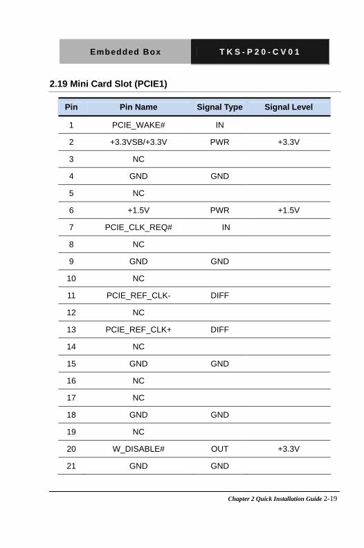
2.19 Mini Card Slot (PCIE1)
Pin Pin Name Signal Type Signal Level
1 PCIE_WAKE# IN
2 +3.3VSB/+3.3V PWR +3.3V
3 NC
4 GND GND
5 NC
6 +1.5V PWR +1.5V
7 PCIE_CLK_REQ# IN
8 NC
9 GND GND
10 NC
11 PCIE_REF_CLK- DIFF
12 NC
13 PCIE_REF_CLK+ DIFF
14 NC
15 GND GND
16 NC
17 NC
18 GND GND
19 NC
20 W_DISABLE# OUT +3.3V
21 GND GND

Embedded Box T K S - P 2 0 - C V 0 1
Chapter 2 Quick Installation Guide 2-20
22 PCIE_RST# OUT +3.3V
23 PCIE_RX-/ mSATA_RX+ DIFF
24 +3.3VSB/+3.3V PWR +3.3V
25 PCIE_RX+/mSATA_RX- DIFF
26 GND GND
27 GND GND
28 +1.5V PWR +1.5V
29 GND GND
30 SMB_CLK I/O +3.3V
31 PCIE_TX-/mSATA_TX- DIFF
32 SMB_DATA I/O +3.3V
33 PCIE_TX+/mSATA_TX+ DIFF
34 GND GND
35 GND GND
36 USB8_D- DIFF
37 GND GND
38 USB8_D+ DIFF
39 +3.3VSB/+3.3V PWR +3.3V
40 GND GND
41 +3.3VSB/+3.3V PWR +3.3V
42 NC
43 GND/NC GND
44 NC
45 NC

Embedded Box T K S - P 2 0 - C V 0 1
Chapter 2 Quick Installation Guide 2-21
46 NC
47 NC
48 +1.5V PWR +1.5V
49 NC
50 GND GND
51 NC
52 +3.3VSB/+3.3V PWR +3.3V

Embedded Box T K S - P 2 0 - C V 0 1
Chapter 2 Quick Installation Guide 2-22
Below Table for China RoHS Requirements
产品中有毒有害物质或元素名称及含量
AAEON Main Board/ Daughter Board/ Backplane
有毒有害物质或元素
部件名称 铅
(Pb)
汞
(Hg)
镉
(Cd)
六价铬
(Cr(VI))
多溴联苯
(PBB)
多溴二苯醚
(PBDE)
印刷电路板
及其电子组件× ○ ○ ○ ○ ○
外部信号
连接器及线材× ○ ○ ○ ○ ○
O:表示该有毒有害物质在该部件所有均质材料中的含量均在 SJ/T 11363-2006 标准规定的限量要求以下。
X:表示该有毒有害物质至少在该部件的某一均质材料中的含量超出
SJ/T 11363-2006 标准规定的限量要求。 备注:此产品所标示之环保使用期限,系指在一般正常使用状况下。

Embedded Box T K S - P 2 0 - C V 0 1
Chapter 3 AMI BIOS Setup 3-1
AMI
Chapter
3BIOS Setup

Embedded Box T K S - P 2 0 - C V 0 1
3.1 System Test and Iinitialization
These routines test and initialize board hardware. If the routines
encounter an error during the tests, you will either hear a few short
beeps or see an error message on the screen. There are two kinds
of errors: fatal and non-fatal. The system can usually continue the
boot up sequence with non-fatal errors.
System configuration verification
These routines check the current system configuration stored in the
CMOS memory and BIOS NVRAM. If system configuration is not
found or system configuration data error is detected, system will
load optimized default and re-boot with this default system
configuration automatically.
There are four situations in which you will need to setup system
configuration:
1. You are starting your system for the first time
2. You have changed the hardware attached to your system
3. The system configuration is reset by Clear-CMOS jumper
4. The CMOS memory has lost power and the configuration
information has been erased.
The TKS-P20-CV01 CMOS memory has an integral lithium battery
backup for data retention. However, you will need to replace the
Chapter 3 AMI BIOS Setup 3-2

Embedded Box T K S - P 2 0 - C V 0 1
complete unit when it finally runs down.
3.2 AMI BIOS Setup
AMI BIOS ROM has a built-in Setup program that allows users to
modify the basic system configuration. This type of information is
stored in battery-backed CMOS RAM and BIOS NVRAM so that it
retains the Setup information when the power is turned off.
Entering Setup
Power on the computer and press <Del>or <F2> immediately. This
will allow you to enter Setup.
Main
Set the date, use tab to switch between date elements.
Advanced
Enable disable boot option for legacy network devices.
Chipset
Host bridge parameters.
Boot
Enables/disable quiet boot option.
Security
Set setup administrator password.
Save & Exit
Exit system setup after saving the changes.
Chapter 3 AMI BIOS Setup 3-3

Embedded Box T K S - P 2 0 - C V 0 1
Setup Menu
Setup submenu: Main
Options summary: (default setting)
System Date Day MM:DD:YYYY
Change the month, year and century. The ‘Day’ is changed automatically.
System Time HH : MM : SS
Change the clock of the system.
Chapter 3 AMI BIOS Setup 3-4

Embedded Box T K S - P 2 0 - C V 0 1
Setup submenu: Advanced
Options summary: (default setting)
ACPI Settings
System ACPI Parameters
CPU Configuration
CPU Configuration Parameters
IDE Configuration
IDE Device Options Settings
USB Configuration
USB Configuration Parameters
COM Port Configuration
Chapter 3 AMI BIOS Setup 3-5

Embedded Box T K S - P 2 0 - C V 0 1
COM Port Configuration Parameters
Digital IO Port Configuration
DIO configuration
H/W Monitor
Monitor hardware status
ACPI Settings
Options summary: (default setting)
Enabled Enable Hibernation
Disabled
Enabled or disabled hibernate (OS/S4 Sleep State).
Chapter 3 AMI BIOS Setup 3-6
Embedded Box T K S - P 2 0 - C V 0 1
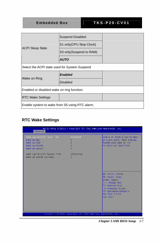
Suspend Disabled
S1 only(CPU Stop Clock)
S3 only(Suspend to RAM) ACPI Sleep State
AUTO
Select the ACPI state used for System Suspend
Enabled Wake on Ring
Disabled
Enabled or disabled wake on ring function.
RTC Wake Settings
Enable system to wake from S5 using RTC alarm.
RTC Wake Settings
Chapter 3 AMI BIOS Setup 3-7
Embedded Box T K S - P 2 0 - C V 0 1
Options summary: (default setting)
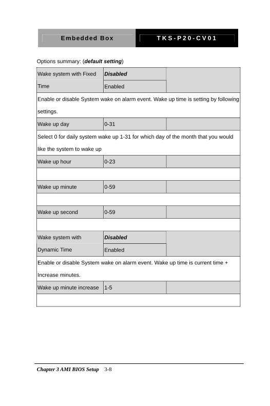
Disabled Wake system with Fixed
Time Enabled
Enable or disable System wake on alarm event. Wake up time is setting by following
settings.
Wake up day 0-31
Select 0 for daily system wake up 1-31 for which day of the month that you would
like the system to wake up
Wake up hour 0-23
Wake up minute 0-59
Wake up second 0-59
Disabled Wake system with
Dynamic Time Enabled
Enable or disable System wake on alarm event. Wake up time is current time +
Increase minutes.
Wake up minute increase 1-5
Chapter 3 AMI BIOS Setup 3-8

Embedded Box T K S - P 2 0 - C V 0 1
CPU Configuration
Options summary: (default setting)
Disabled Hyper-Threading
Enabled
En/Disable CPU Hyper-Threading function
Disabled Execute Disable Bit
Enabled
En/Disable XD bit for supporting OS
Disabled Limit CPUID Maximum
Enabled
Disabled for Windows XP
Chapter 3 AMI BIOS Setup 3-9

Embedded Box T K S - P 2 0 - C V 0 1
CPU Power Management
Configure CPU PPM parameters
CPU Power Management
Options summary: (default setting)
Disabled EIST
Enabled
En/Disable Intel SpeedStep
Disabled CPU C State Report
Enabled
Chapter 3 AMI BIOS Setup 3-10

Embedded Box T K S - P 2 0 - C V 0 1
Report C State support for ACPI OS
IDE Configuration
Options summary: (default setting)
Disabled SATA Controller(s)
Enabled
En/Disable SATA controller
IDE Configure SATA as
AHCI
Configure SATA controller operating as IDE/AHCI mode.
Chapter 3 AMI BIOS Setup 3-11

Embedded Box T K S - P 2 0 - C V 0 1
USB Configuration
Options summary: (default setting)
Enabled
Disabled
Legacy USB Support
Auto
Enables BIOS Support for Legacy USB Support. When enabled, USB can be
functional in legacy environment like DOS. AUTO option disables legacy support if
no USB devices are connected. DISABLE option will keep USB devices available
only for EFI application
Auto Device Name
(Emulation Type) Floppy
Chapter 3 AMI BIOS Setup 3-12

Embedded Box T K S - P 2 0 - C V 0 1
Forced FDD
Hard Disk
CD-ROM
If Auto. USB devices less than 530MB will be emulated as Floppy and remaining as
Floppy and remaining as hard drive. Forced FDD option can be used to force a
HDD formatted drive to boot as FDD(Ex. ZIP drive)
COM Port Configuration
Options summary: (default setting)
Serial Port 1/2 Configuration
Set Parameters of Serial Port 1/2
Chapter 3 AMI BIOS Setup 3-13

Embedded Box T K S - P 2 0 - C V 0 1
Serial Port 1 Configuration
Options summary: (default setting)
Disabled Serial Port
Enabled
En/Disable specified serial port.
Auto
IO=3F8h; IRQ=4;
IO=3F8h; IRQ=3,4,5,7,10,11,12;
IO=2F8h; IRQ=3,4,5,7,10,11,12;
IO=3E8h; IRQ=3,4,5,7,10,11,12;
Change Settings
IO=2E8h; IRQ=3,4,5,7,10,11,12;
Chapter 3 AMI BIOS Setup 3-14

Embedded Box T K S - P 2 0 - C V 0 1
Select a resource setting for Super IO device.
Serial Port 2 Configuration
Options summary: (default setting)
Disabled Serial Port
Enabled
En/Disable specified serial port.
Auto
IO=2F8h; IRQ=3;
IO=3F8h; IRQ=3,4,5,7,10,11,12;
Change Settings
IO=2F8h; IRQ=3,4,5,7,10,11,12;
Chapter 3 AMI BIOS Setup 3-15

Embedded Box T K S - P 2 0 - C V 0 1
IO=3E8h; IRQ=3,4,5,7,10,11,12;
IO=2E8h; IRQ=3,4,5,7,10,11,12;
Select a resource setting for Super IO device.
RS232
RS422
Device Type
RS485
Configure COM2 operated as RS232, RS422 or RS485.
Digital IO Port Configuration
Options summary: (default setting)
GPIO1/GPIO2 Input
Chapter 3 AMI BIOS Setup 3-16

Embedded Box T K S - P 2 0 - C V 0 1
Direction Output
Set GPIO1/GPIO2 as Input or Output
Input GPIO3/GPIO4
Direction Output
Set GPIO3/GPIO4 as Input or Output
Hi Output Level
Low
Set GPIO Level when used as Output
H/W Monitor
Chapter 3 AMI BIOS Setup 3-17

Embedded Box T K S - P 2 0 - C V 0 1
Setup submenu: Chipset
Options summary: (default setting)
Host Bridge
Host Bridge Parameters
South Bridge
South Bridge Parameters
Chapter 3 AMI BIOS Setup 3-18

Embedded Box T K S - P 2 0 - C V 0 1
Host Bridge
Options summary: (default setting)
128MB Fixed Graphics Memory
Size 256MB
Configure Fixed Graphics Memory Size
Auto Detect
CRT
IGFX - Boot Type
HDMI
Select Primary boot display device
Chapter 3 AMI BIOS Setup 3-19

Embedded Box T K S - P 2 0 - C V 0 1
South Bridge
Options summary: (default setting)
Onboard Devices
Onboard devices parameters configurations
mSATA MiniCard Function
PCIe
Switch miniCard function to mSATA or PCIe
Auto
Enabled
PCIe MiniCard Slot
Disabled
Control the PCI Express Root Port.
Chapter 3 AMI BIOS Setup 3-20

Embedded Box T K S - P 2 0 - C V 0 1
Enabled High Precision Timer
Disabled
Enable or Disable the High Precision Event Timer
1-2 Seconds
2-3 Seconds
3-4 Seconds
SLP_S4 Assertion Width
4-5 Seconds
Select a minimum assertion width of the SLP_S4# signal
Power On
Power Off
Restore AC Power Loss
Last State
Select AC power state when power is re-applied after a power failure.
Chapter 3 AMI BIOS Setup 3-21

Embedded Box T K S - P 2 0 - C V 0 1
Onboard Devices
Options summary: (default setting)
Disabled Azalia Controller
HD Audio
Enable or disabled Azalia controller
Disabled LAN Controller
Enabled
Enable or disable Realtek R8111E PCIE Lan Device
Disabled SMBus Controller
Enabled
Enable or Disable OnChip SMBus Controller
Chapter 3 AMI BIOS Setup 3-22

Embedded Box T K S - P 2 0 - C V 0 1
Setup submenu: Boot
Options summary: (default setting)
Disabled Quiet Boot
Enabled
En/Disable showing boot logo.
Disabled Launch LAN PXE OpROM
Enabled
En/Disable PXE boot for RTL8111E LAN
Boot Option #X/
XXXX Drive BBS Priorities
The order of boot priorities.
Chapter 3 AMI BIOS Setup 3-23

Embedded Box T K S - P 2 0 - C V 0 1
BBS Priorities
Options summary: (default setting)
Disabled Boot Option #x
Device name
Sets the system boot order
Chapter 3 AMI BIOS Setup 3-24

Embedded Box T K S - P 2 0 - C V 0 1
Setup submenu: Security
Options summary: (default setting)
Not set Administrator Password/
User Password
You can install a Supervisor password, and if you install a supervisor password, you
can then install a user password. A user password does not provide access to many
of the features in the Setup utility.
Install the Password:
Press Enter on this item, a dialog box appears which lets you enter a password. You
can enter no more than six letters or numbers. Press Enter after you have typed in
the password. A second dialog box asks you to retype the password for
confirmation. Press Enter after you have retyped it correctly. The password is
Chapter 3 AMI BIOS Setup 3-25
Embedded Box T K S - P 2 0 - C V 0 1
required at boot time, or when the user enters the Setup utility.
Removing the Password:
Highlight this item and type in the current password. At the next dialog box press
Enter to disable password protection.
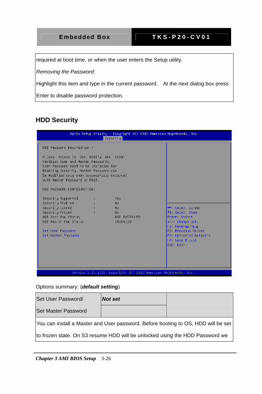
HDD Security
Options summary: (default setting)
Not set Set User Password/
Set Master Password
You can install a Master and User password. Before booting to OS, HDD will be set
to frozen state. On S3 resume HDD will be unlocked using the HDD Password we
Chapter 3 AMI BIOS Setup 3-26

Embedded Box T K S - P 2 0 - C V 0 1
entered while system booting.
Install the Password:
Press Enter on this item, a dialog box appears which lets you enter a password. You
can enter no more than six letters or numbers. Press Enter after you have typed in
the password. A second dialog box asks you to retype the password for
confirmation. Press Enter after you have retyped it correctly. The password is
required at boot time, or when the user enters the Setup utility.
Removing the Password:
Highlight this item and type in the current password. At the next dialog box press
Enter to disable password protection.
Chapter 3 AMI BIOS Setup 3-27

Embedded Box T K S - P 2 0 - C V 0 1
Setup submenu: Exit
Options summary: (default setting)
Save Changes and Reset
Reset the system after saving the changes
Discard Changes and Reset
Reset system setup without saving any changes
Restore Defaults
Restore/Load Default values for all the setup options.
Save as User Defaults
Save the changes done so far as User Defaults
Restore User Defaults
Chapter 3 AMI BIOS Setup 3-28

Embedded Box T K S - P 2 0 - C V 0 1
Chapter 3 AMI BIOS Setup 3-29
Restore the User Defaults to all the setup options

Embedded Box T K S - P 2 0 - C V 0 1
Chapter 4 Driver Installation 4 -1
Driver
Chapter
4Installation
.

Embedded Box T K S - P 2 0 - C V 0 1
The TKS-P20-CV01 comes with an AutoRun DVD-ROM that
contains all drivers and utilities that can help you to install the driver
automatically.
Insert the driver DVD, the driver DVD-title will auto start and show
the installation guide. If not, please follow the sequence below to
install the drivers.
Follow the sequence below to install the drivers:
Step 1 – Install Chipset Driver
Step 2 – Install VGA Driver
Step 3 – Install AHCI Driver
Step 4 – Install LAN Driver
Step 5 – Install Audio Driver
Step 6 – Serial Port Driver (Optional)
Please read instructions below for further detailed installations.
Chapter 4 Driver Installation 4 -2

Embedded Box T K S - P 2 0 - C V 0 1
4.1 Installation:
Insert the TKS-P20-CV01 DVD-ROM into the DVD-ROM drive. And
install the drivers from Step 1 to Step 6 in order.
Step 1 – Install Chipset Driver
1. Click on the STEP1-CHIPSET folder and select the OS
folder your system is
2. Double click on the infinst_autol_1034.exe file located in
each OS folder
3. Follow the instructions that the window shows
4. The system will help you install the driver automatically
Step 2 – Install VGA Driver
For Windows® 7
1. Click on the STEP2-VGA folder and select the folder of WIN7_32
2. Double click on the Setup.exe file
3. Follow the instructions that the window shows
4. The system will help you install the driver automatically
For Windows® XP
1. Install Framework 3.5
Double click on the dotnetfx35.exe
Follow the instructions that the window shows
The system will help you install the driver
automatically
Chapter 4 Driver Installation 4 -3

Embedded Box T K S - P 2 0 - C V 0 1
2. Install IEMGD
Double click on the SETUP.exe
Select the configuration
Follow the instructions that the window shows
The system will help you install the driver
automatically
Chapter 4 Driver Installation 4 -4

Embedded Box T K S - P 2 0 - C V 0 1
If you want to update driver, please uninstall driver first.
Uninstall IEMGD
1. Double click on the SETUP.exe
2. Follow the instructions that the window shows
3. The system will help you uninstall the driver automatically
Chapter 4 Driver Installation 4 -5

Embedded Box T K S - P 2 0 - C V 0 1
Step 3 – Install AHCI Driver
Please refer to the Appendix D AHCI Setting
Step 4 – Install LAN Driver
1. Click on the STEP4-LAN folder and select the OS folder
your system is
2. Double click on the setup.exe file located in each OS
folder
3. Follow the instructions that the window shows
4. The system will help you install the driver automatically
Step 5 – Install Audio Driver
1. Click on the STEP5-AUDIO folder and select the OS
folder your system is
2. Double click on the Setup.exe file located in each OS
folder
3. Follow the instructions that the window shows
4. The system will help you install the driver automatically
Step 6– Serial Port Driver (Optional)
For Windows® XP:
1. Click on the STEP6-Serial Port Driver (Optional) and
select the folder of WINXP_32
2. Double click on patch.bat file
3. Follow the instructions that the window shows
Chapter 4 Driver Installation 4 -6

Embedded Box T K S - P 2 0 - C V 0 1
4. The system will help you install the driver automatically
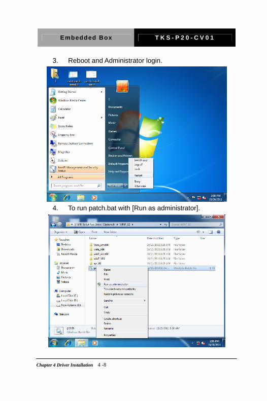
For Windows® 7:
1. Create a password for Administrator account.
2. Change User Account Control Settings to [Never notify]
Chapter 4 Driver Installation 4 -7
Embedded Box T K S - P 2 0 - C V 0 1
Chapter 4 Driver Installation 4 -8
3. Reboot and Administrator login.
4. To run patch.bat with [Run as administrator].

Embedded Box T K S - P 2 0 - C V 0 1
Appendix A Programming the Watchdog Timer A-1
Programming the
Appendix
AWatchdog Timer

Embedded Box T K S - G 2 1 - C V 0 5
Appendix A Programming the Watchdog Timer A-2
A.1 Watchdog Timer Registers
Table 1 : Watch dog relative IO address Default Value Note
I/O Base
Address 0xA00
I/O Base address for Watchdog operation.
This address is assigned by SIO LDN7, register 0x60‐0x61.
Table 2 : Watchdog relative register table
Register Offset BitNum Value Note
Watchdog
WDTRST# Enable 0x00 7 1
Enable/Disable
time out output via WDTRST#
0: Disable
1: Enable
Pulse Width 0x05 0:1 01
Width of Pulse signal
00: 1ms (do not use)
01: 25ms
10: 125ms
11: 5s
Pulse width is must longer then
16ms.
Signal Polarity 0x05 2 0
0: low active
1: high active
Must set this bit to 0
Counting Unit 0x05 3 0
Select time unit.
0: second
1: minute
Output Signal
Type 0x05 4 1
0: Level
1: Pulse
Must set this bit to 1
Watchdog Timer
Enable 0x05 5 1
0: Disable
1: Enable
Timeout Status 0x05 6 1 1: timeout occurred. Write a 1
to clear timeout status
Timer Counter 0x06 Time of watchdog timer
(0~255)

Embedded Box T K S - P 2 0 - C V 0 1
Appendix A Programming the Watchdog Timer A-3
A.2 WatchDog Sample Program
******************************************************************************
// WDT I/O operation relative definition (Please reference to Table 1)
#define WDTAddr 0xA00 // WDT I/O base address
Void WDTWriteByte(byte Register, byte Value);
byte WDTReadByte(byte Register);
Void WDTSetReg(byte Register, byte Bit, byte Val);
// Watch Dog relative definition (Please reference to Table 2)
#define DevReg 0x00 // Device configuration register
#define WDTRstBit 0x80 // Watchdog WDTRST# (Bit7)
#define WDTRstVal 0x80 // Enabled WDTRST#
#define TimerReg 0x05 // Timer register
#define PSWidthBit 0x00 // WDTRST# Pulse width (Bit0:1)
#define PSWidthVal 0x01 // 25ms for WDTRST# pulse
#define PolarityBit 0x02 // WDTRST# Signal polarity (Bit2)
#define PolarityVal 0x00 // Low active for WDTRST#
#define UnitBit 0x03 // Unit for timer (Bit3)
#define ModeBit 0x04 // WDTRST# mode (Bit4)
#define ModeVal 0x01 // 0:level 1: pulse
#define EnableBit 0x05 // WDT timer enable (Bit5)
#define EnableVal 0x01 // 1: enable
#define StatusBit 0x06 // WDT timer status (Bit6)
#define CounterReg 0x06 // Timer counter register
*******************************************************************************
*******************************************************************************
VOID Main(){ // Procedure : AaeonWDTConfig
// (byte)Timer : Counter of WDT timer.(0x00~0xFF)
// (boolean)Unit : Select time unit(0: second, 1: minute).
AaeonWDTConfig(Counter, Unit);
// Procedure : AaeonWDTEnable
// This procudure will enable the WDT counting.

Embedded Box T K S - G 2 1 - C V 0 5
Appendix A Programming the Watchdog Timer A-4
AaeonWDTEnable();
}
*******************************************************************************
*******************************************************************************
// Procedure : AaeonWDTEnable
VOID AaeonWDTEnable (){
WDTEnableDisable(1);
}
// Procedure : AaeonWDTConfig
VOID AaeonWDTConfig (byte Counter, BOOLEAN Unit){
// Disable WDT counting
WDTEnableDisable(0);
// Clear Watchdog Timeout Status
WDTClearTimeoutStatus();
// WDT relative parameter setting
WDTParameterSetting(Timer, Unit);
}
VOID WDTEnableDisable(byte Value){
If (Value == 1)
WDTSetBit(TimerReg, EnableBit, 1);
else
WDTSetBit(TimerReg, EnableBit, 0);
}
VOID WDTParameterSetting(byte Counter, BOOLEAN Unit){
// Watchdog Timer counter setting
WDTWriteByte(CounterReg, Counter);
// WDT counting unit setting
WDTSetBit(TimerReg, UnitBit, Unit);
// WDT output mode set to pulse
WDTSetBit(TimerReg, ModeBit, ModeVal);
// WDT output mode set to active low
WDTSetBit(TimerReg, PolarityBit, PolarityVal);
// WDT output pulse width is 25ms

Embedded Box T K S - P 2 0 - C V 0 1
Appendix A Programming the Watchdog Timer A-5
WDTSetBit(TimerReg, PSWidthBit, PSWidthVal);
// Watchdog WDTRST# Enable
WDTSetBit(DevReg, WDTRstBit, WDTRstVal);
}
VOID WDTClearTimeoutStatus(){
WDTSetBit(TimerReg, StatusBit, 1);
}
*******************************************************************************
*******************************************************************************
VOID WDTWriteByte(byte Register, byte Value){
IOWriteByte(WDTAddr+Register, Value);
}
byte WDTReadByte(byte Register){
return IOReadByte(WDTAddr+Register);
}
VOID WDTSetBit(byte Register, byte Bit, byte Val){
byte TmpValue;
TmpValue = WDTReadByte(Register);
TmpValue &= ~(1 << Bit);
TmpValue |= Val << Bit;
WDTWriteByte(Register, TmpValue);
}
*******************************************************************************

Embedded Box T K S - P 2 0 - C V 0 1
Appendix B I/O Information B-1
I/O Information
Appendix
B

Embedded Box T K S - P 2 0 - C V 0 1
Appendix B I/O Information B-2
B.1 I/O Address Map

Embedded Box T K S - P 2 0 - C V 0 1
Appendix B I/O Information B-3

Embedded Box T K S - P 2 0 - C V 0 1
Appendix B I/O Information B-4
B.2 Memory Address Map

Embedded Box T K S - P 2 0 - C V 0 1
Appendix B I/O Information B-5
B.3 IRQ Mapping Chart

Embedded Box T K S - P 2 0 - C V 0 1
Appendix B I/O Information B-6

Embedded Box T K S - P 2 0 - C V 0 1
Appendix B I/O Information B-7
B.4 DMA Channel Assignments

Embedded Box T K S - P 2 0 - C V 0 1
Appendix C Mating Connector C - 1
Mating Connector
Appendix
C

Embedded Box T K S - P 2 0 - C V 0 1
Appendix C Mating Connector C - 2
C.1 List of Mating Connectors and Cables
The table notes mating connectors and available cables.
Mating Connector Connector Label
Function
Vendor Model number
Available Cable
Cable P/N
CN1 COM1 Port CATCH 1201-700-09SSerial Port Cable
1701090150
CN2 COM2 Port CATCH 1201-700-09SSerial Port Cable
1701090150
CN3 Digital I/O CATCH 1201-700-06S
AAEON DIO ExtensionCable
1701060150
CN4 +5V Output for SATA HDD
CATCH 1192-700-02S
2 Pins for SATA PWR Cable
1702150155
CN5 SATA Port ASTRON 97-0912HA-7-R
7-Pin 50cm SATA Cable
1709070500
CN6 External 12V Input
CATCH 1191-700-04SPWR Cable
170204010S
CN7 RJ-45 Ethernet
UDE RT7-17FAAM1A
N/A N/A
CN8 Buzzer CATCH 1201-700-02SBuzzer Cable
170302010C
CN9
Audio Line In/Out and MIC Connector
CATCH 1201-700-10SAudio Cable
1709100254
CN10 LPC Expansion I/F
CATCH 1204-700-12SAAEON LPC Cable
1703120130

Embedded Box T K S - P 2 0 - C V 0 1
Appendix C Mating Connector C - 3
CN11 USB Port 5 CATCH 1201-700-05SUSB Port Cable
1700050207
CN12 Analog CRT Display
ASTRON HDLH-B15-CFHN1T-1-R
N/A N/A
CN13 USB Port 3 CATCH 1201-700-05SUSB Port Cable
1700050207
CN14 USB Port 4 CATCH 1201-700-05SUSB Port Cable
1700050207
CN15 18-bit LVDS Output
E-Call 0110-01-553-200
N/A N/A
CN16 USB Port 1 and 2
TechBest KS-002D-ANB(2.0)-L
N/A N/A
CN17 HDMI Type C ASTRON 360FC19-0N002T-R
N/A N/A
CN18
LVDS Inverter/ Backlight Connector
CATCH 1192-700-05S N/A N/A
CN19 Front Panel JVE 21B22050-XXS
10B-01G-4/2
AAEON Front Panel Cable
1701100156
BAT1 External RTC Battery Connector
CATCH 1201-700-02S Battery Cable
175011901M

Embedded Box T K S - P 2 0 - C V 0 1
Appendix D AHCI Setting D-1
AHCI Setting
A ppendix
D

Embedded Box T K S - P 2 0 - C V 0 1
Appendix D AHCI Setting D-2
D.1 Setting AHCI
OS installation to SETUP AHCI Mode
Step 1: Copy below files from “Driver CD -> STEP3-AHCI \WinXP_32” and
to diskette.
Step 2: Connect the USB Floppy drive to the board and insert the diskette
from previous step.
Step 3: Configure SATA Controller to RAID mode in BIOS SETUP Menu:
Advanced -> IDE Configuration -> SATA Mode -> AHCI Mode

Embedded Box T K S - P 2 0 - C V 0 1
Appendix D AHCI Setting D-3
Step 4: Configure DVD/CD-ROM drive as the first boot device.
Step 5: Save changes and exit BIOS SETUP

Embedded Box T K S - P 2 0 - C V 0 1
Appendix D AHCI Setting D-4
Step 6 – Boot to DVD/CD-ROM device to install OS
Step 7 – Press “F6” to install AHCI driver
Step 8 – Press “S” to install AHCI driver
Step 9 – Choose “Intel(R) ICH7R/DH SATA AHCI Controller”
Step 10 – Windows Setup will display the controller name you selected in
previous step and continue to install OS when ”ENTER” pressed.

Embedded Box T K S - P 2 0 - C V 0 1
Appendix E Digital I/O Ports E-1
Digital I/O Ports
Appendix
E
Embedded Box T K S - P 2 0 - C V 0 1
Appendix E Digital I/O Ports E-2
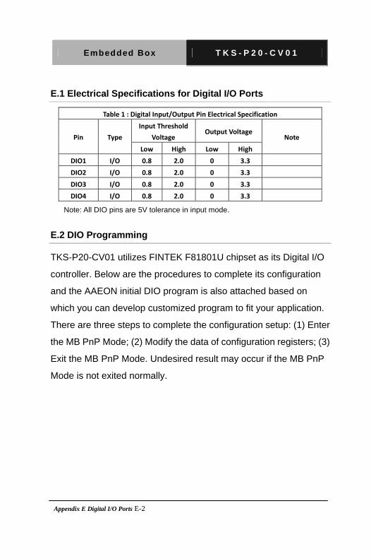
E.1 Electrical Specifications for Digital I/O Ports
Table 1 : Digital Input/Output Pin Electrical Specification
Input Threshold
Voltage Output Voltage
Pin Type
Low High Low High
Note
DIO1 I/O 0.8 2.0 0 3.3
DIO2 I/O 0.8 2.0 0 3.3
DIO3 I/O 0.8 2.0 0 3.3
DIO4 I/O 0.8 2.0 0 3.3
Note: All DIO pins are 5V tolerance in input mode.
E.2 DIO Programming
TKS-P20-CV01 utilizes FINTEK F81801U chipset as its Digital I/O
controller. Below are the procedures to complete its configuration
and the AAEON initial DIO program is also attached based on
which you can develop customized program to fit your application.
There are three steps to complete the configuration setup: (1) Enter
the MB PnP Mode; (2) Modify the data of configuration registers; (3)
Exit the MB PnP Mode. Undesired result may occur if the MB PnP
Mode is not exited normally.

Embedded Box T K S - P 2 0 - C V 0 1
Appendix E Digital I/O Ports E-3
E.3 Digital I/O Register
Table 2 : SuperIO relative register table
Default Value Note
Index 0x2E SIO MB PnP Mode Index Register
0x2E or 0x4E
Data 0x2F) SIO MB PnP Mode Data Register
0x2F or 0x4F
Table 3 : Digital Input/Output relative register table
LDN Register BitNum Note
GPIO1 Direction 0x06 0xD0 0 0:input, 1: output
GPIO2 Direction 0x06 0xD0 1
GPIO3 Direction 0x06 0xD0 2
GPIO4 Direction 0x06 0xD0 3
GPIO1 Output Level 0x06 0xD1 0 0:low, 1: high
GPIO2 Output Level 0x06 0xD1 1
GPIO3 Output Level 0x06 0xD1 2
GPIO4 Output Level 0x06 0xD1 3
GPIO1 Status 0x06 0xD2 0 0:low, 1: high
GPIO2 Status 0x06 0xD2 1
GPIO3 Status 0x06 0xD2 2
GPIO4 Status 0x06 0xD2 3

Embedded Box T K S - P 2 0 - C V 0 1
Appendix E Digital I/O Ports E-4
E.4 Digital I/O Sample Program
**************************************************************************
// SuperIO relative definition (Please reference to Table 2)
#define SIOIndex 0x2E
#define SIOData 0x2F
#define DIOLDN 0x06
IOWriteByte(byte IOPort, byte Value);
IOReadByte(byte IOPort);
// DIO relative definition (Please reference to Table 3)
#define DirReg 0xD0 // 0:input, 1: output
#define InputPin 0x00
#define OutputPin 0x01
#define OutputReg 0xD1 // 0:low, 1: high
#define StatusReg 0xD2 // 0:low, 1: high
#define PinLow 0x00
#define PinHigh 0x01
#define Pin1Bit 0x00
#define Pin2Bit 0x01
#define Pin3Bit 0x02
#define Pin4Bit 0x03
**************************************************************************
**************************************************************************
VOID Main(){ Boolean PinStatus ;
// Procedure : AaeonReadPinStatus
// Input :
// Example, Read Digital I/O Pin 3 status
// Output :
// InputStatus :
// 0: Digital I/O Pin level is low
// 1: Digital I/O Pin level is High
PinStatus = AaeonReadPinStatus(Pin3Bit);
// Procedure : AaeonSetOutputLevel

Embedded Box T K S - P 2 0 - C V 0 1
Appendix E Digital I/O Ports E-5
// Input :
// Example, Set Digital I/O Pin 2 to high level
AaeonSetOutputLevel(Pin2Bit, PinHigh);
}
**************************************************************************
**************************************************************************
Boolean AaeonReadPinStatus(byte PinBit){
Boolean PinStatus ;
PinStatus = SIOBitRead(DIOLDN, StatusReg, PinBit);
Return PinStatus ;
}
VOID AaeonSetOutputLevel(byte PinBit, byte Value){
ConfigDioMode(PinBit, OutputPin);
SIOBitSet(DIOLDN, OutputReg, PinBit, Value);
}
**************************************************************************
******
**************************************************************************
******VOID SIOEnterMBPnPMode(){
IOWriteByte(SIOIndex, 0x87);
IOWriteByte(SIOIndex, 0x87);
}
VOID SIOExitMBPnPMode(){
IOWriteByte(SIOIndex, 0xAA);
}
VOID SIOSelectLDN(byte LDN){
IOWriteByte(SIOIndex, 0x07); // SIO LDN Register Offset = 0x07
IOWriteByte(SIOData, LDN);
}
VOID SIOBitSet(byte LDN, byte Register, byte BitNum, byte Value){
Byte TmpValue;

Embedded Box T K S - P 2 0 - C V 0 1
Appendix E Digital I/O Ports E-6
SIOEnterMBPnPMode();
SIOSelectLDN(LDN);
IOWriteByte(SIOIndex, Register);
TmpValue = IOReadByte(SIOData);
TmpValue &= ~(1 << BitNum);
TmpValue |= (Value << BitNum);
IOWriteByte(SIOData, TmpValue);
SIOExitMBPnPMode();
}
VOID SIOByteSet(byte LDN, byte Register, byte Value){
SIOEnterMBPnPMode();
SIOSelectLDN(LDN);
IOWriteByte(SIOIndex, Register);
IOWriteByte(SIOData, Value);
SIOExitMBPnPMode();
}
**************************************************************************
******


![Probabilistic and Decision-Theoretic User Modeling in the ... · [HBH+98, CV01]). We do not pursue the debate between adaptable versus adaptive systems. Instead, we focus on adaptive](https://img.pdfslide.us/doc/110x75/6039c0978837c2024466b67f/probabilistic-and-decision-theoretic-user-modeling-in-the-hbh98-cv01-we.jpg)