Embed Size (px)
Citation preview
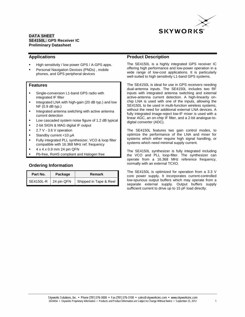
DATA SHEET SE4150L: GPS Receiver IC Preliminary Datasheet
Skyworks Solutions, Inc. • Phone [781] 376-3000 • Fax [781] 376-3100 • [email protected] • www.skyworksinc.com 202445A • Skyworks Proprietary Information • Products and Product Information are Subject to Change Without Notice • September 25, 2012 1
Applications
High sensitivity / low power GPS / A-GPS apps. Personal Navigation Devices (PNDs) , mobile
phones, and GPS peripheral devices
Features
Single-conversion L1-band GPS radio with integrated IF filter
Integrated LNA with high-gain (20 dB typ.) and low NF (0.9 dB typ.)
Integrated antenna switching with active antenna current detection
Low cascaded system noise figure of 1.2 dB typical 2-bit SIGN & MAG digital IF output 2.7 V - 3.6 V operation Standby current <10 µA Fully integrated PLL synthesizer, VCO & loop filter
compatible with 16.368 MHz ref. frequency 4 x 4 x 0.9 mm 24 pin QFN Pb-free, RoHS compliant and Halogen free
Ordering Information
Part No. Package Remark
SE4150L-R 24 pin QFN Shipped in Tape & Reel
Product Description The SE4150L is a highly integrated GPS receiver IC offering high performance and low-power operation in a wide range of low-cost applications. It is particularly well-suited to high sensitivity L1-band GPS systems. The SE4150L is ideal for use in GPS receivers needing dual-antenna inputs. The SE4150L includes two RF inputs with integrated antenna switching and external active-antenna current detection. A high-linearity on-chip LNA is used with one of the inputs, allowing the SE4150L to be used in multi-function wireless systems, without the need for additional external LNA devices. A fully integrated image-reject low-IF mixer is used with a linear AGC, an on-chip IF filter, and a 2-bit analogue-to-digital converter (ADC). The SE4150L features two gain control modes, to optimize the performance of the LNA and mixer for systems which either require high signal handling, or systems which need minimal supply current. The SE4150L synthesizer is fully integrated including the VCO and PLL loop-filter. The synthesizer can operate from a 16.368 MHz reference frequency, normally with an external TCXO. The SE4150L is optimized for operation from a 3.3 V core power supply. It incorporates current-controlled low-spurious output buffers which may operate from a separate external supply. Output buffers supply sufficient current to drive up to 15 pF load directly.

DATA SHEET SE4150L: GPS Receiver IC Preliminary Datasheet
Skyworks Solutions, Inc. • Phone [781] 376-3000 • Fax [781] 376-3100 • [email protected] • www.skyworksinc.com 202445A • Skyworks Proprietary Information • Products and Product Information are Subject to Change Without Notice • September 25, 2012 2
Functional Block Diagram
SIGN
SE4150L
Phase /Freq.
Detector
Quadrature÷2 Feedback
Divider
IF Filter
~~~
VCO
-45°
+45°
ADC
~
AGCController
I Q
VCC_TCXOTCXO IN
VAGC
CLK_OUT
ChipControl
RX_EN
MAG
RVI
LNBuffer
Optionalfilter
LNA_IN
ANT_SW_OUT MIX_IN
PLL LoopFilter Reference
Buffer
Mix Gain
ANT1_IN
AntennaCurrentDetect
ANT_FEED
ANT_BIAS
ANT_DET
ChargePump
PLL
LNA
HW_0
HW_1
CLK_EN
LNA Gain
Filter Gain
To External ActiveAntenna
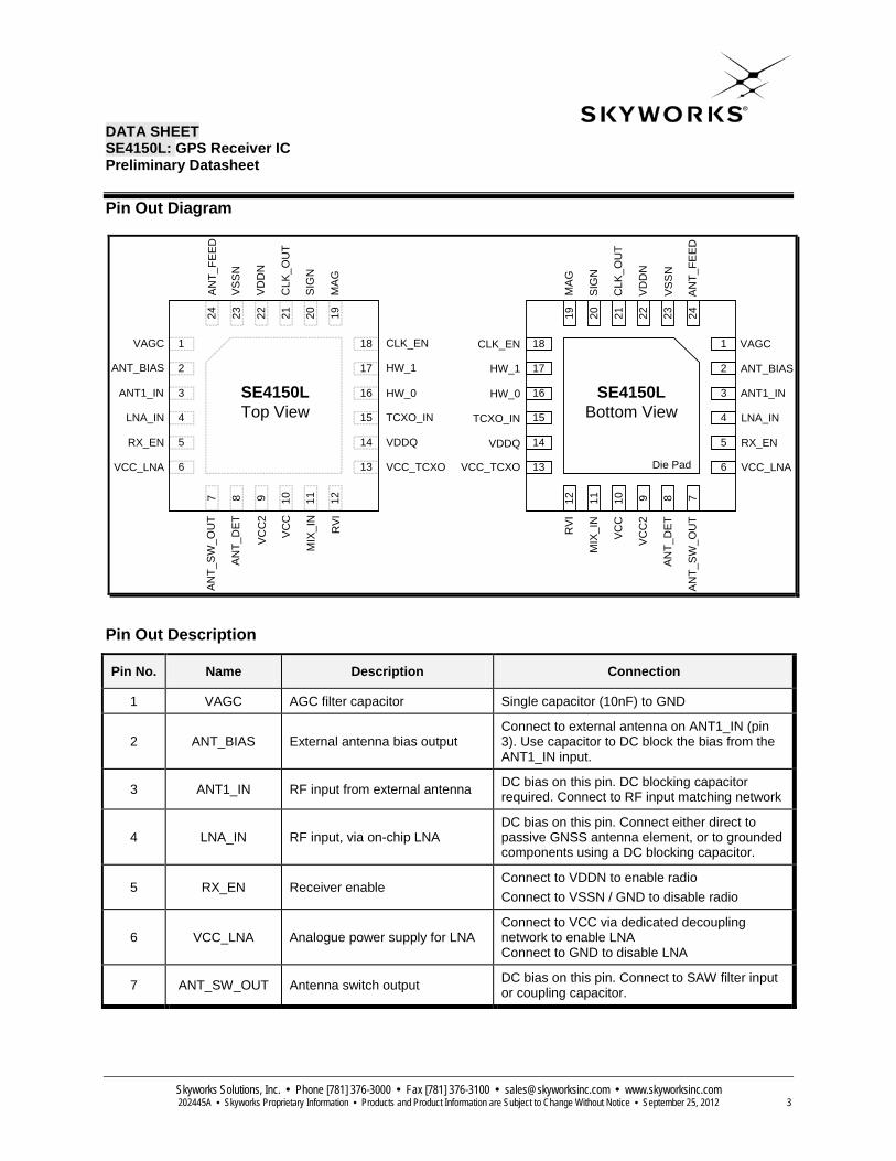
DATA SHEET SE4150L: GPS Receiver IC Preliminary Datasheet
Skyworks Solutions, Inc. • Phone [781] 376-3000 • Fax [781] 376-3100 • [email protected] • www.skyworksinc.com 202445A • Skyworks Proprietary Information • Products and Product Information are Subject to Change Without Notice • September 25, 2012 3
Pin Out Diagram
AN
T_FE
ED
AN
T_FE
ED
18
15
17
16
14
13
1
4
2
3
5
6
2421 23222019
710 891112
SE4150LBottom View
Die Pad
18
15
17
16
14
13
1
4
2
3
5
6
24 2123 22 20 19
7 108 9 11 12
SE4150LTop View
VD
DN
MA
G
CLK
_OU
T
CLK_EN
SIG
N
RV
I
AN
T_D
ET
MIX
_IN
VC
C
AN
T_S
W_O
UT
VC
C2
RX_EN
VAGC
VCC_LNA
ANT_BIAS
ANT1_IN
LNA_IN TCXO_IN
VCC_TCXO
HW_1
VDDQ
HW_0
TCXO_IN
HW_1
HW_0
RX_EN
VAGC
VCC_LNA
ANT1_IN
LNA_IN
ANT_BIAS
VC
C
MIX
_IN
AN
T_S
W_O
UT
AN
T_D
ET
VD
DN
CLK
_OU
T
SIG
N
MA
G
CLK_EN
VC
C2
RV
I
VDDQ
VS
SN
VS
SN
VCC_TCXO
Pin Out Description
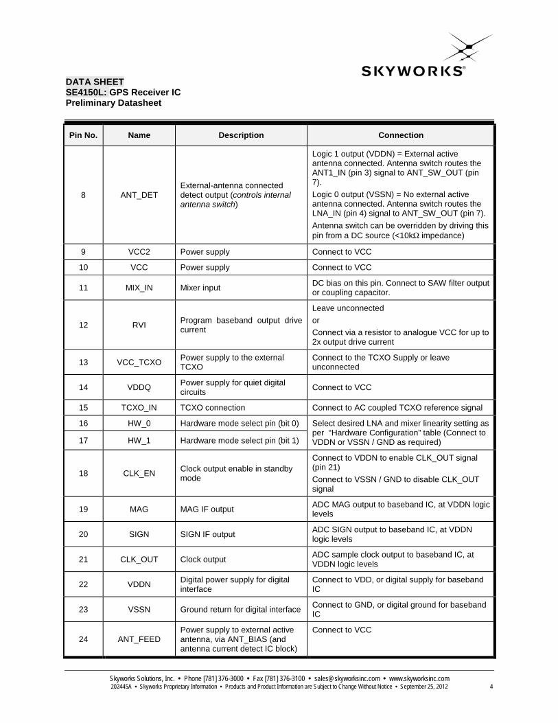
Pin No. Name Description Connection
1 VAGC AGC filter capacitor Single capacitor (10nF) to GND
2 ANT_BIAS External antenna bias output Connect to external antenna on ANT1_IN (pin 3). Use capacitor to DC block the bias from the ANT1_IN input.
3 ANT1_IN RF input from external antenna DC bias on this pin. DC blocking capacitor required. Connect to RF input matching network
4 LNA_IN RF input, via on-chip LNA DC bias on this pin. Connect either direct to passive GNSS antenna element, or to grounded components using a DC blocking capacitor.
5 RX_EN Receiver enable Connect to VDDN to enable radio Connect to VSSN / GND to disable radio
6 VCC_LNA Analogue power supply for LNA Connect to VCC via dedicated decoupling network to enable LNA Connect to GND to disable LNA
7 ANT_SW_OUT Antenna switch output DC bias on this pin. Connect to SAW filter input or coupling capacitor.
DATA SHEET SE4150L: GPS Receiver IC Preliminary Datasheet
Skyworks Solutions, Inc. • Phone [781] 376-3000 • Fax [781] 376-3100 • [email protected] • www.skyworksinc.com 202445A • Skyworks Proprietary Information • Products and Product Information are Subject to Change Without Notice • September 25, 2012 4
Pin No. Name Description Connection
8 ANT_DET External-antenna connected detect output (controls internal antenna switch)
Logic 1 output (VDDN) = External active antenna connected. Antenna switch routes the ANT1_IN (pin 3) signal to ANT_SW_OUT (pin 7). Logic 0 output (VSSN) = No external active antenna connected. Antenna switch routes the LNA_IN (pin 4) signal to ANT_SW_OUT (pin 7). Antenna switch can be overridden by driving this pin from a DC source (<10kΩ impedance)
9 VCC2 Power supply Connect to VCC
10 VCC Power supply Connect to VCC
11 MIX_IN Mixer input DC bias on this pin. Connect to SAW filter output or coupling capacitor.
12 RVI Program baseband output drive current
Leave unconnected or Connect via a resistor to analogue VCC for up to 2x output drive current
13 VCC_TCXO Power supply to the external TCXO
Connect to the TCXO Supply or leave unconnected
14 VDDQ Power supply for quiet digital circuits Connect to VCC
15 TCXO_IN TCXO connection Connect to AC coupled TCXO reference signal
16 HW_0 Hardware mode select pin (bit 0) Select desired LNA and mixer linearity setting as per “Hardware Configuration” table (Connect to VDDN or VSSN / GND as required) 17 HW_1 Hardware mode select pin (bit 1)
18 CLK_EN Clock output enable in standby mode
Connect to VDDN to enable CLK_OUT signal (pin 21) Connect to VSSN / GND to disable CLK_OUT signal
19 MAG MAG IF output ADC MAG output to baseband IC, at VDDN logic levels
20 SIGN SIGN IF output ADC SIGN output to baseband IC, at VDDN logic levels
21 CLK_OUT Clock output ADC sample clock output to baseband IC, at VDDN logic levels
22 VDDN Digital power supply for digital interface
Connect to VDD, or digital supply for baseband IC
23 VSSN Ground return for digital interface Connect to GND, or digital ground for baseband IC
24 ANT_FEED Power supply to external active antenna, via ANT_BIAS (and antenna current detect IC block)
Connect to VCC
DATA SHEET SE4150L: GPS Receiver IC Preliminary Datasheet
Skyworks Solutions, Inc. • Phone [781] 376-3000 • Fax [781] 376-3100 • [email protected] • www.skyworksinc.com 202445A • Skyworks Proprietary Information • Products and Product Information are Subject to Change Without Notice • September 25, 2012 5
Pin No. Name Description Connection
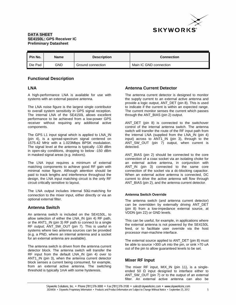
Die Pad GND Ground connection Main IC GND connection
Functional Description
LNA A high-performance LNA is available for use with systems with an external passive antenna. The LNA noise figure is the largest single contributor to overall system sensitivity in GPS signal reception. The internal LNA of the SE4150L allows excellent performance to be achieved from a low-power GPS receiver without requiring any additional active components. The GPS L1 input signal which is applied to LNA_IN (pin 4), is a spread-spectrum signal centered on 1575.42 MHz with a 1.023Mbps BPSK modulation. The signal level at the antenna is typically -130 dBm in open-sky conditions, dropping to below -150 dBm in masked signal areas (e.g. indoors). The LNA input requires a minimum of external matching components to achieve good RF gain with minimal noise figure. Although attention should be paid to track lengths and interference throughout the design, the LNA input matching circuit is the only RF circuit critically sensitive to layout. The LNA output includes internal 50Ω matching for connection to the mixer input, either directly or via an optional external filter. Antenna Switch An antenna switch is included on the SE4150L, to allow selection of either the LNA_IN (pin 4) RF path, or the ANT1_IN (pin 3) RF path to connect to a single RF output; ANT_SW_OUT (pin 7). This is useful in systems where two antenna sources can be provided (e.g. a PND, where an internal antenna and a socket for an external antenna are available). The antenna switch is driven from the antenna current detector block. The antenna switch will transfer the RF input from the default LNA_IN (pin 4) over to ANT1_IN (pin 3), when the antenna current detector block senses a current being consumed, for example, from an external active antenna. The switching threshold is typically 1mA with some hysteresis.
Antenna Current Detector The antenna current detector is designed to monitor the supply current to an external active antenna and provide a logic output, ANT_DET (pin 8). This is used to indicate if the current is within an expected range. The current monitor senses the current which passes through the ANT_BIAS (pin 2) output. ANT_DET (pin 8) is connected to the switchover control of the internal antenna switch. The antenna switch will transfer the route of the RF input path from the internal LNA (supplied from the LNA_IN (pin 4) input) across to ANT1_IN (pin 3), through to the ANT_SW_OUT (pin 7) output, when current is detected. ANT_BIAS (pin 2) should be connected to the core connection of a coax socket via an isolating choke for an external active antenna, in conjunction with ANT_IN (pin 3) connected to the same core connection of the socket via a dc-blocking capacitor. When an external active antenna is connected, DC current to drive the active antenna will flow through ANT_BIAS (pin 2), and the antenna current detector. Antenna Switch Override
The antenna switch (and antenna current detector) can be overridden by externally driving ANT_DET (pin 8) from a low-impedance external source, at VDDN (pin 22) or GND levels. This can be useful, for example, in applications where the external antenna is not powered by the SE4150L feed, or to facilitate user override via the host processor man-machine interface. The external source applied to ANT_DET (pin 8) must be able to source >300 uA into the pin, or sink >70 uA out of the pin to allow guaranteed levels to be set.
Mixer RF Input The mixer RF input, MIX_IN (pin 11), is a single-ended 50 Ω input designed to interface either to ANT_SW_OUT (pin 7) or to the output of an external filter. An external active antenna can also be
DATA SHEET SE4150L: GPS Receiver IC Preliminary Datasheet
Skyworks Solutions, Inc. • Phone [781] 376-3000 • Fax [781] 376-3100 • [email protected] • www.skyworksinc.com 202445A • Skyworks Proprietary Information • Products and Product Information are Subject to Change Without Notice • September 25, 2012 6
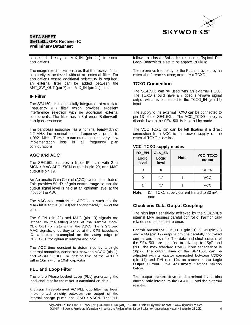
connected directly to MIX_IN (pin 11) in some applications. The image reject mixer ensures that the receiver’s full sensitivity is achieved without an external filter. For applications where additional selectivity is required, an external filter can be added between the ANT_SW_OUT (pin 7) and MIX_IN (pin 11) pins. IF Filter The SE4150L includes a fully integrated Intermediate Frequency (IF) filter which provides excellent interference rejection with no additional external components. The filter has a 3rd order Butterworth bandpass response. The bandpass response has a nominal bandwidth of 2.2 MHz; the nominal center frequency is preset to 4.092 MHz. These parameters ensure very low implementation loss in all frequency plan configurations. AGC and ADC The SE4150L features a linear IF chain with 2-bit SIGN / MAG ADC. SIGN output is pin 20, and MAG output is pin 19. An Automatic Gain Control (AGC) system is included. This provides 50 dB of gain control range so that the output signal level is held at an optimum level at the input of the ADC. The MAG data controls the AGC loop, such that the MAG bit is active (HIGH) for approximately 33% of the time. The SIGN (pin 20) and MAG (pin 19) signals are latched by the falling edge of the sample clock, CLK_OUT (pin 21) within the ADC. The SIGN and MAG signals, once they arrive at the GPS baseband IC, are best re-sampled on the rising edge of CLK_OUT, for optimum sample and hold. The AGC time constant is determined by a single external capacitor, connected between VAGC (pin 1), and VSSN / GND. The settling-time of the AGC is within 10ms with a 10nF capacitor. PLL and Loop Filter The entire Phase-Locked Loop (PLL) generating the local oscillator for the mixer is contained on-chip. A classic three-element RC PLL loop filter has been implemented on-chip between the output of the internal charge pump and GND / VSSN. The PLL
follows a classic 3rd-order response. Typical PLL Loop- Bandwidth is set to be approx. 200kHz. The reference frequency for the PLL is provided by an external reference source; normally a TCXO. TCXO Connection The SE4150L can be used with an external TCXO. The TCXO should have a clipped sinewave signal output which is connected to the TCXO_IN (pin 15) input. The supply to the external TCXO can be connected to pin 13 of the SE4150L. The VCC_TCXO supply is disabled when the SE4150L is in stand-by mode. The VCC_TCXO pin can be left floating if a direct connection from VCC to the power supply of the external TCXO is desired. VCC_TCXO supply modes
RX_EN Logic level
CLK_EN Logic level
Note VCC_TCXO output
‘0’ ‘0’ - OPEN
‘0’ ‘1’ 1 VCC
‘1’ ‘1’ 1 VCC
Note: (1) TCXO supply current limited to 30 mA max.
Clock and Data Output Coupling The high input sensitivity achieved by the SE4150L’s internal LNA requires careful control of harmonically related sources of interference. For this reason the CLK_OUT (pin 21), SIGN (pin 20) and MAG (pin 19) outputs provide carefully controlled current and slew-rate. The data and clock outputs of the SE4150L are specified to drive up to 15pF load (N.B. the max standard CMOS input capacitance is 10pF). The output drive of the SE4150L can be adjusted with a resistor connected between VDDQ (pin 14) and RVI (pin 12), as shown in the Logic Output Current Drive Adjustment Settings section below. The output current drive is determined by a bias current ratio internal to the SE4150L and the external resistor.

DATA SHEET SE4150L: GPS Receiver IC Preliminary Datasheet
Skyworks Solutions, Inc. • Phone [781] 376-3000 • Fax [781] 376-3100 • [email protected] • www.skyworksinc.com 202445A • Skyworks Proprietary Information • Products and Product Information are Subject to Change Without Notice • September 25, 2012 7
Hardware Configuration The SE4150L can be configured to change the LNA Gain/Linearity and the Mixer Gain/Linearity by means of the settings on the HW_0 (pin 16) and HW_1 (pin 17) logic inputs. The adjustment of the gain and linearity allow the SE4150L to be used in differing environments, either with significant co-located interference sources (e.g. mobile phone) or no interference sources (e.g. PND). LNA Gain & Linearity Selection The SE4150L supports two settings for gain and input IP3 in the on-chip LNA. Supported LNA Gain & Linearity Modes
LNA Mode
LNA Gain LNA IIP3
Hi Gain 20 dB -6 dBm
Lo Gain 17 dB -12 dBm
Mixer Gain Selection The SE4150L supports two gain settings for the on-chip mixer.
Supported Mixer Gain Modes
Mixer Mode
Mixer Buffer Gain
Hi Gain 32 dB
Lo Gain 24 dB
The following truth table gives the settings for hardware configuration of both the LNA Gain/Linearity and also the Mixer Gain/Linearity. Hardware Configuration
LNA Mode Mixer Mode Selection value (HW_<1:0>)
Hi Gain Hi Gain 11
Lo Gain Lo Gain 00
Power Management The SE4150L uses RX_EN (pin 5) to put the device into standby. In standby mode, all circuits are off and the device consumes only leakage current. The RX_EN input has a 200 kΩ pull-down resistor to GND, on-chip. This ensures that the RFIC will put itself in standby when the RX_EN controller on the baseband is tri-stated to an impedance much greater than 200 kΩ. The internal LNA can be disabled by connecting the Vcc supply connection to the LNA, VCC_LNA (pin 6) to GND. This may be desirable in some applications, and prevents the LNA from consuming any current, saving approximately 5mA. The sample clock output, CLK_OUT (pin 21) can be kept active by setting CLK_EN (pin 18) pin to logic ‘1’ (HI). This will cause all circuits required to produce the CLK_OUT signal to remain active, even when the receiver is forced into Standby mode (RX_EN (pin 5) set to Logic ‘0’). Logic Interfacing The SE4150L Logic Inputs can either be driven from an external baseband IC, or permanently set by connecting to either VDDN (pin 22) for Logic ‘1’, or GND for Logic ‘0’. The digital interface on the SE4150L, supplied from VDDN, has been designed to operate at the same voltage as the GPS baseband IC. The ANT_DET (pin 8) output is sourced from the antenna current detector, and is also connected to the internal antenna switch; the switch toggles the RF signal source automatically when an external active antenna is connected. The antenna current detector can be overridden by applying a low impedance source (<10kΩ impedance) at VDDN (pin 22) or GND levels to ANT_DET (pin 8), such as a logic output from a GPIO pin on the GPS Baseband IC. This means that automatic switching can be activated by leaving the GPIO pin on the Baseband IC in a high impedance state, or overridden by setting to the appropriate state. The SE4150L Logic Input and Output signals are shown in the following tables:
DATA SHEET SE4150L: GPS Receiver IC Preliminary Datasheet
Skyworks Solutions, Inc. • Phone [781] 376-3000 • Fax [781] 376-3100 • [email protected] • www.skyworksinc.com 202445A • Skyworks Proprietary Information • Products and Product Information are Subject to Change Without Notice • September 25, 2012 8
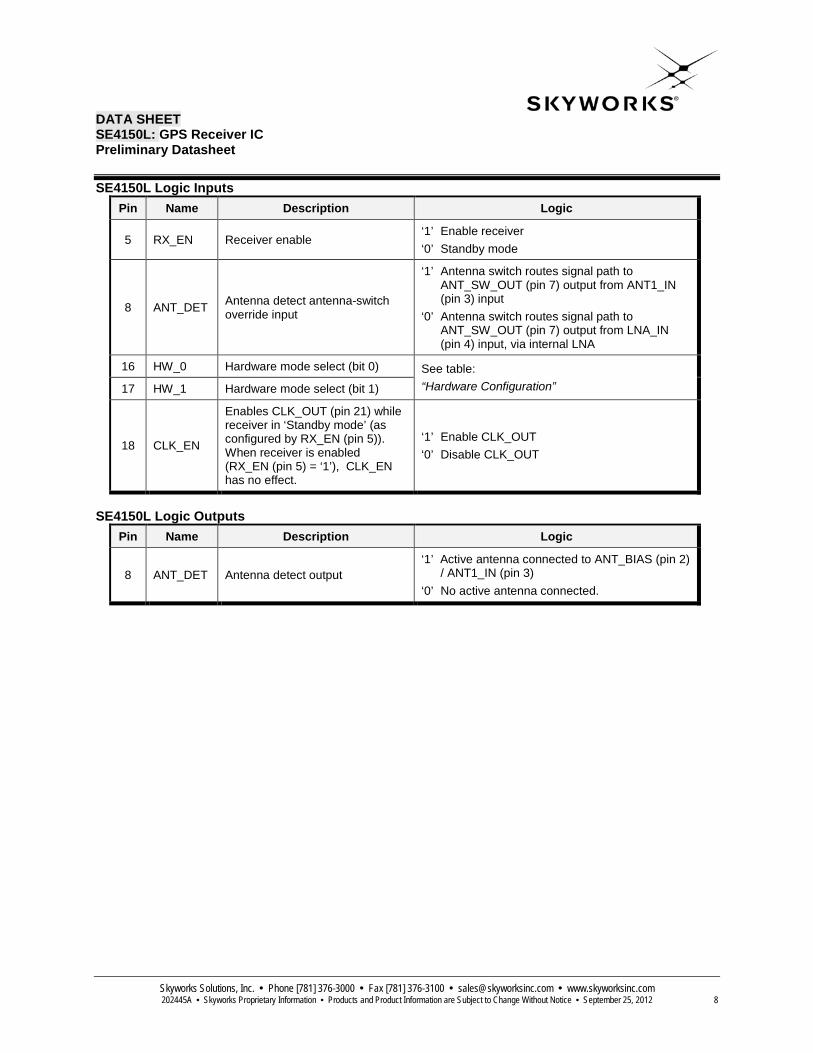
SE4150L Logic Inputs Pin Name Description Logic
5 RX_EN Receiver enable ‘1’ Enable receiver ‘0’ Standby mode
8 ANT_DET Antenna detect antenna-switch override input
‘1’ Antenna switch routes signal path to ANT_SW_OUT (pin 7) output from ANT1_IN (pin 3) input
‘0’ Antenna switch routes signal path to ANT_SW_OUT (pin 7) output from LNA_IN (pin 4) input, via internal LNA
16 HW_0 Hardware mode select (bit 0) See table: “Hardware Configuration” 17 HW_1 Hardware mode select (bit 1)
18 CLK_EN
Enables CLK_OUT (pin 21) while receiver in ‘Standby mode’ (as configured by RX_EN (pin 5)). When receiver is enabled (RX_EN (pin 5) = ‘1’), CLK_EN has no effect.
‘1’ Enable CLK_OUT ‘0’ Disable CLK_OUT
SE4150L Logic Outputs
Pin Name Description Logic
8 ANT_DET Antenna detect output ‘1’ Active antenna connected to ANT_BIAS (pin 2)
/ ANT1_IN (pin 3) ‘0’ No active antenna connected.
DATA SHEET SE4150L: GPS Receiver IC Preliminary Datasheet
Skyworks Solutions, Inc. • Phone [781] 376-3000 • Fax [781] 376-3100 • [email protected] • www.skyworksinc.com 202445A • Skyworks Proprietary Information • Products and Product Information are Subject to Change Without Notice • September 25, 2012 9
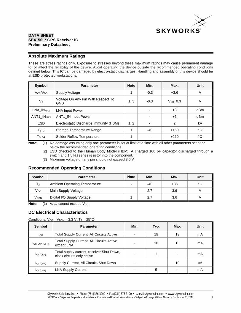
Absolute Maximum Ratings These are stress ratings only. Exposure to stresses beyond these maximum ratings may cause permanent damage to, or affect the reliability of the device. Avoid operating the device outside the recommended operating conditions defined below. This IC can be damaged by electro-static discharges. Handling and assembly of this device should be at ESD protected workstations.
Symbol Parameter Note Min. Max. Unit
VCC/VDD Supply Voltage 1 -0.3 +3.6 V
VX Voltage On Any Pin With Respect To GND 1, 3 -0.3 VDD+0.3 V
LNA_INMAX LNA Input Power - +3 dBm
ANT1_INMAX ANT1_IN Input Power - +3 dBm
ESD Electrostatic Discharge Immunity (HBM) 1, 2 - 2 kV
TSTG Storage Temperature Range 1 -40 +150 °C
TSLDR Solder Reflow Temperature 1 - +260 °C
Note: (1) No damage assuming only one parameter is set at limit at a time with all other parameters set at or below the recommended operating conditions.
(2) ESD checked to the Human Body Model (HBM). A charged 100 pF capacitor discharged through a switch and 1.5 kΩ series resistor into the component.
(3) Maximum voltage on any pin should not exceed 3.6 V Recommended Operating Conditions
Symbol Parameter Note Min. Max. Unit
TA Ambient Operating Temperature - -40 +85 °C
VCC Main Supply Voltage 2.7 3.6 V
VDDN Digital I/O Supply Voltage 1 2.7 3.6 V
Note: (1) VDDN cannot exceed VCC DC Electrical Characteristics Conditions: VCC = VDDN = 3.3 V, TA = 25°C
Symbol Parameter Min. Typ. Max. Unit
ICC Total Supply Current, All Circuits Active - 15 18 mA
ICC(LNA_OFF) Total Supply Current, All Circuits Active except LNA - 10 13 mA
ICC(CLK) Total supply current, receiver Shut Down, clock circuits only active - 1 - mA
ICC(OFF) Supply Current, All Circuits Shut Down - - 10 µA
ICC(LNA) LNA Supply Current - 5 - mA
DATA SHEET SE4150L: GPS Receiver IC Preliminary Datasheet
Skyworks Solutions, Inc. • Phone [781] 376-3000 • Fax [781] 376-3100 • [email protected] • www.skyworksinc.com 202445A • Skyworks Proprietary Information • Products and Product Information are Subject to Change Without Notice • September 25, 2012 10
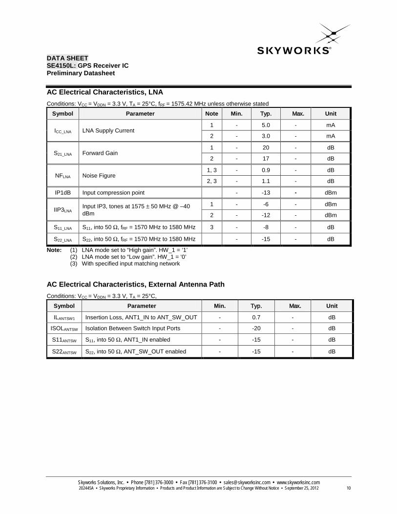
AC Electrical Characteristics, LNA Conditions: VCC = VDDN = 3.3 V, TA = 25°C, fRF = 1575.42 MHz unless otherwise stated
Symbol Parameter Note Min. Typ. Max. Unit
ICC_LNA LNA Supply Current 1 - 5.0 - mA
2 - 3.0 - mA
S21_LNA Forward Gain 1 - 20 - dB
2 - 17 - dB
NFLNA Noise Figure 1, 3 - 0.9 - dB
2, 3 - 1.1 - dB
IP1dB Input compression point - -13 - dBm
IIP3LNA Input IP3, tones at 1575 ± 50 MHz @ –40 dBm
1 - -6 - dBm
2 - -12 - dBm
S11_LNA S11, into 50 Ω, fRF = 1570 MHz to 1580 MHz 3 - -8 - dB
S22_LNA S22, into 50 Ω, fRF = 1570 MHz to 1580 MHz - -15 - dB
Note: (1) LNA mode set to “High gain”. HW_1 = ‘1’ (2) LNA mode set to “Low gain”. HW_1 = ‘0’ (3) With specified input matching network
AC Electrical Characteristics, External Antenna Path Conditions: VCC = VDDN = 3.3 V, TA = 25°C,
Symbol Parameter Min. Typ. Max. Unit
ILANTSW1 Insertion Loss, ANT1_IN to ANT_SW_OUT - 0.7 - dB
ISOLANTSW Isolation Between Switch Input Ports - -20 - dB
S11ANTSW S11, into 50 Ω, ANT1_IN enabled - -15 - dB
S22ANTSW S22, into 50 Ω, ANT_SW_OUT enabled - -15 - dB
DATA SHEET SE4150L: GPS Receiver IC Preliminary Datasheet
Skyworks Solutions, Inc. • Phone [781] 376-3000 • Fax [781] 376-3100 • [email protected] • www.skyworksinc.com 202445A • Skyworks Proprietary Information • Products and Product Information are Subject to Change Without Notice • September 25, 2012 11
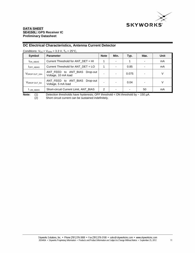
DC Electrical Characteristics, Antenna Current Detector Conditions: VCC = VDDN = 3.3 V, TA = 25°C,
Symbol Parameter Note Min. Typ. Max. Unit
ION_ABIAS Current Threshold for ANT_DET = HI 1 - 1 - mA
IOFF_ABIAS Current Threshold for ANT_DET = LO 1 - 0.85 - mA
VDROP OUT_10m ANT_FEED to ANT_BIAS Drop-out Voltage, 10 mA load - - 0.075 - V
VDROP OUT_5m ANT_FEED to ANT_BIAS Drop-out Voltage, 5 mA load - - 0.04 - V
I LIM_ABIAS Short-circuit Current Limit, ANT_BIAS 2 - - 50 mA
Note: (1) Detection thresholds have hysteresis; OFF threshold < ON threshold by ~ 150 µA. (2) Short circuit current can be sustained indefinitely.
DATA SHEET SE4150L: GPS Receiver IC Preliminary Datasheet
Skyworks Solutions, Inc. • Phone [781] 376-3000 • Fax [781] 376-3100 • [email protected] • www.skyworksinc.com 202445A • Skyworks Proprietary Information • Products and Product Information are Subject to Change Without Notice • September 25, 2012 12
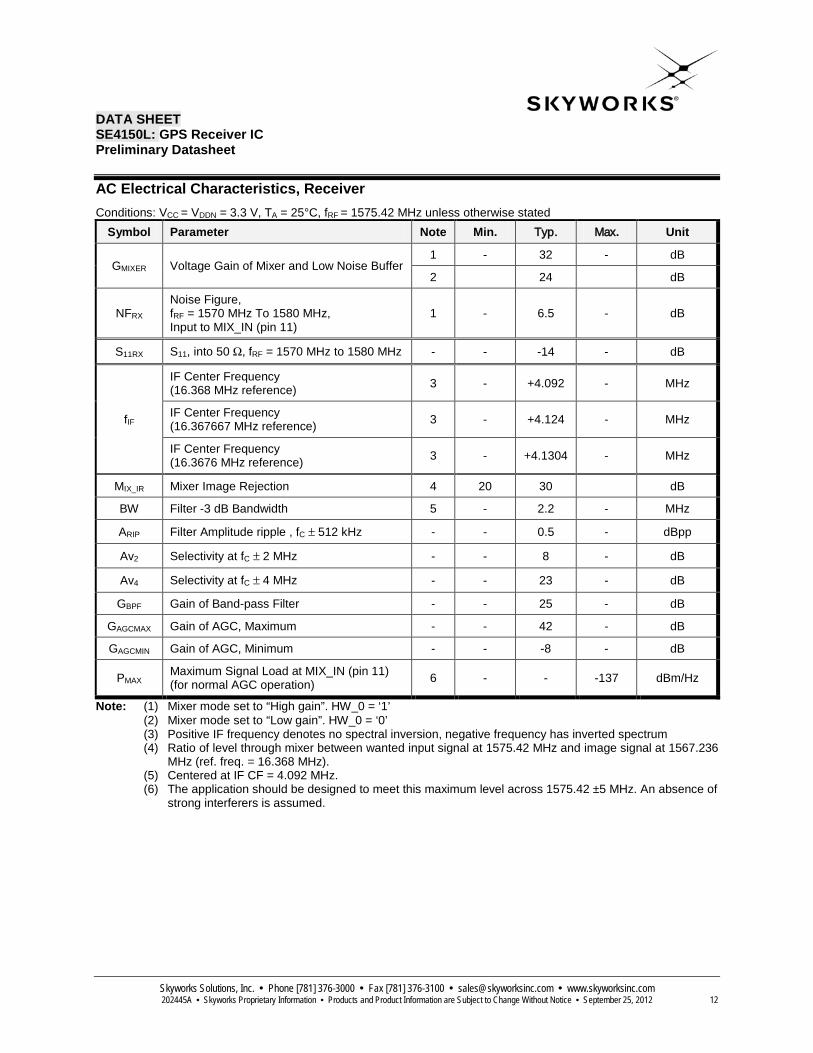
AC Electrical Characteristics, Receiver Conditions: VCC = VDDN = 3.3 V, TA = 25°C, fRF = 1575.42 MHz unless otherwise stated
Symbol Parameter Note Min. Typ. Max. Unit
GMIXER Voltage Gain of Mixer and Low Noise Buffer 1 - 32 - dB
2 24 dB
NFRX Noise Figure, fRF = 1570 MHz To 1580 MHz, Input to MIX_IN (pin 11)
1 - 6.5 - dB
S11RX S11, into 50 Ω, fRF = 1570 MHz to 1580 MHz - - -14 - dB
fIF
IF Center Frequency (16.368 MHz reference) 3 - +4.092 - MHz
IF Center Frequency (16.367667 MHz reference) 3 - +4.124 - MHz
IF Center Frequency (16.3676 MHz reference) 3 - +4.1304 - MHz
MIX_IR Mixer Image Rejection 4 20 30 dB
BW Filter -3 dB Bandwidth 5 - 2.2 - MHz
ARIP Filter Amplitude ripple , fC ± 512 kHz - - 0.5 - dBpp
Av2 Selectivity at fC ± 2 MHz - - 8 - dB
Av4 Selectivity at fC ± 4 MHz - - 23 - dB
GBPF Gain of Band-pass Filter - - 25 - dB
GAGCMAX Gain of AGC, Maximum - - 42 - dB
GAGCMIN Gain of AGC, Minimum - - -8 - dB
PMAX Maximum Signal Load at MIX_IN (pin 11) (for normal AGC operation) 6 - - -137 dBm/Hz
Note: (1) Mixer mode set to “High gain”. HW_0 = ‘1’ (2) Mixer mode set to “Low gain”. HW_0 = ‘0’ (3) Positive IF frequency denotes no spectral inversion, negative frequency has inverted spectrum (4) Ratio of level through mixer between wanted input signal at 1575.42 MHz and image signal at 1567.236
MHz (ref. freq. = 16.368 MHz). (5) Centered at IF CF = 4.092 MHz. (6) The application should be designed to meet this maximum level across 1575.42 ±5 MHz. An absence of
strong interferers is assumed.
DATA SHEET SE4150L: GPS Receiver IC Preliminary Datasheet
Skyworks Solutions, Inc. • Phone [781] 376-3000 • Fax [781] 376-3100 • [email protected] • www.skyworksinc.com 202445A • Skyworks Proprietary Information • Products and Product Information are Subject to Change Without Notice • September 25, 2012 13
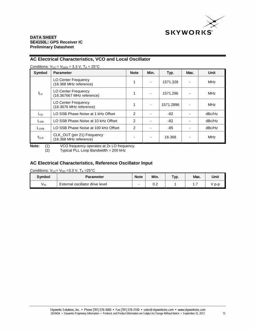
AC Electrical Characteristics, VCO and Local Oscillator Conditions: VCC = VDDN = 3.3 V, TA = 25°C
Symbol Parameter Note Min. Typ. Max. Unit
fLO
LO Center Frequency (16.368 MHz reference) 1 - 1571.328 - MHz
LO Center Frequency (16.367667 MHz reference) 1 - 1571.296 - MHz
LO Center Frequency (16.3676 MHz reference) 1 - 1571.2896 - MHz
L1k LO SSB Phase Noise at 1 kHz Offset 2 - -82 - dBc/Hz
L10k LO SSB Phase Noise at 10 kHz Offset 2 - -82 - dBc/Hz
L100k LO SSB Phase Noise at 100 kHz Offset 2 - -85 - dBc/Hz
fCLK CLK_OUT (pin 21) Frequency (16.368 MHz reference) - - 16.368 - MHz
Note: (1) VCO frequency operates at 2x LO frequency. (2) Typical PLL Loop Bandwidth = 200 kHz
AC Electrical Characteristics, Reference Oscillator Input Conditions: VCC= VDD =3.3 V, TA =25°C
Symbol Parameter Note Min. Typ. Max. Unit
VIN External oscillator drive level - 0.2 1 1.7 V p-p

DATA SHEET SE4150L: GPS Receiver IC Preliminary Datasheet
Skyworks Solutions, Inc. • Phone [781] 376-3000 • Fax [781] 376-3100 • [email protected] • www.skyworksinc.com 202445A • Skyworks Proprietary Information • Products and Product Information are Subject to Change Without Notice • September 25, 2012 14
Logic Level Characteristics – Input Pins Conditions: VCC = VDDN = 3.3 V, TA = 25°C. Applies to logic pins used as inputs: RX_EN (pin 5), HW_0 (pin 16),
HW_1 (pin 17) and CLK_EN (pin 18).
Symbol Parameter Note Min. Typ. Max. Unit
VIH Logic High Input Voltage - 0.7 VDDN - VDDN V
VIL Logic Low Input Voltage - 0 - 0.4 V
IIH Input Current Logic High Voltage - - 200 - nA
IIH_RX_EN Input Current Logic High Voltage for RX_EN Input (pin 5) 1 - 16.5 - μA
IIL Input Current Logic Low Voltage - - -200 - nA
CILOAD Input Load Capacitance - - - 2 pF
Note: (1) Applies to RX_EN (pin 5) only. Figure dominated by 200kΩ (nom) on-chip pull-down resistor. Logic Level Characteristics – Output Pins Conditions: VCC = VDDN = 3.3 V, TA = 25°C. Applies to logic pins used as outputs: CLK_OUT (pin 21), SIGN (pin 20),
and MAG (pin 19).
Symbol Parameter Note Min. Typ. Max. Unit
VOH Logic High Output Voltage - VDDN - 0.1V - VDDN V
VOL Logic Low Output Voltage - 0 - 0.1 V
COLOAD Output Load Capacitance - - - 15 pF
Note: (1) Output Current set at Nominal level; no Current Setting Resistor on RVI (pin 12). Positive value indicates current source; negative value indicates current sink.
ANT_DET (pin 8) Characteristics ANT_DET (pin 8) is an input and output logic signal. In output mode, it operates as an indicator of the current through ANT_BIAS (pin 2). In input mode, an input needs to be applied which overrides the output from the pin, to force the internal antenna-switch.
ANT _BIAS Current Note External Forced I/P on
ANT_DET Isink Impedance to VCC
ANT_DET Output Logic Level
Antenna Switch Signal Path (to ANT_SW_OUT)
<0.85mA 1 - 300 uA ∞ LO (0) LNA_IN
>1mA 2 - 0 uA 50kΩ HI (1) ANT1_IN
<0.85mA 1,3 Low impedance to VCC 150 uA ∞ Forced HI ANT1_IN
>1mA 2 Low impedance to GND 0 uA 100kΩ Forced LO LNA_IN
Note: (1) No external active antenna connected. (2) External active antenna connected
(3) The difference between the internal logic level and the output level is sensed and the output drive is reduced, to save current
DATA SHEET SE4150L: GPS Receiver IC Preliminary Datasheet
Skyworks Solutions, Inc. • Phone [781] 376-3000 • Fax [781] 376-3100 • [email protected] • www.skyworksinc.com 202445A • Skyworks Proprietary Information • Products and Product Information are Subject to Change Without Notice • September 25, 2012 15
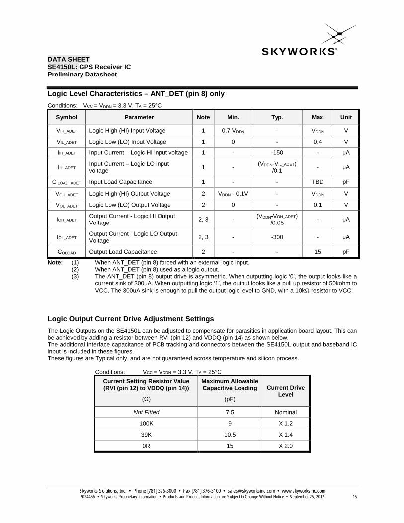
Logic Level Characteristics – ANT_DET (pin 8) only Conditions: VCC = VDDN = 3.3 V, TA = 25°C
Symbol Parameter Note Min. Typ. Max. Unit
VIH_ADET Logic High (HI) Input Voltage 1 0.7 VDDN - VDDN V
VIL_ADET Logic Low (LO) Input Voltage 1 0 - 0.4 V
IIH_ADET Input Current – Logic HI input voltage 1 - -150 - μA
IIL_ADET Input Current – Logic LO input voltage 1 - (VDDN-VIL_ADET)
/0.1 - μA
CILOAD_ADET Input Load Capacitance 1 - - TBD pF
VOH_ADET Logic High (HI) Output Voltage 2 VDDN - 0.1V - VDDN V
VOL_ADET Logic Low (LO) Output Voltage 2 0 - 0.1 V
IOH_ADET Output Current - Logic HI Output Voltage 2, 3 - (VDDN-VOH_ADET)
/0.05 - μA
IOL_ADET Output Current - Logic LO Output Voltage 2, 3 - -300 - μA
COLOAD Output Load Capacitance 2 - - 15 pF
Note: (1) When ANT_DET (pin 8) forced with an external logic input. (2) When ANT_DET (pin 8) used as a logic output. (3) The ANT_DET (pin 8) output drive is asymmetric. When outputting logic ‘0’, the output looks like a
current sink of 300uA. When outputting logic ‘1’, the output looks like a pull up resistor of 50kohm to VCC. The 300uA sink is enough to pull the output logic level to GND, with a 10kΩ resistor to VCC.
Logic Output Current Drive Adjustment Settings The Logic Outputs on the SE4150L can be adjusted to compensate for parasitics in application board layout. This can be achieved by adding a resistor between RVI (pin 12) and VDDQ (pin 14) as shown below. The additional interface capacitance of PCB tracking and connectors between the SE4150L output and baseband IC input is included in these figures. These figures are Typical only, and are not guaranteed across temperature and silicon process. Conditions: VCC = VDDN = 3.3 V, TA = 25°C
Current Setting Resistor Value (RVI (pin 12) to VDDQ (pin 14))
(Ω)
Maximum Allowable Capacitive Loading
(pF)
Current Drive Level
Not Fitted 7.5 Nominal
100K 9 X 1.2
39K 10.5 X 1.4
0R 15 X 2.0
DATA SHEET SE4150L: GPS Receiver IC Preliminary Datasheet
Skyworks Solutions, Inc. • Phone [781] 376-3000 • Fax [781] 376-3100 • [email protected] • www.skyworksinc.com 202445A • Skyworks Proprietary Information • Products and Product Information are Subject to Change Without Notice • September 25, 2012 16
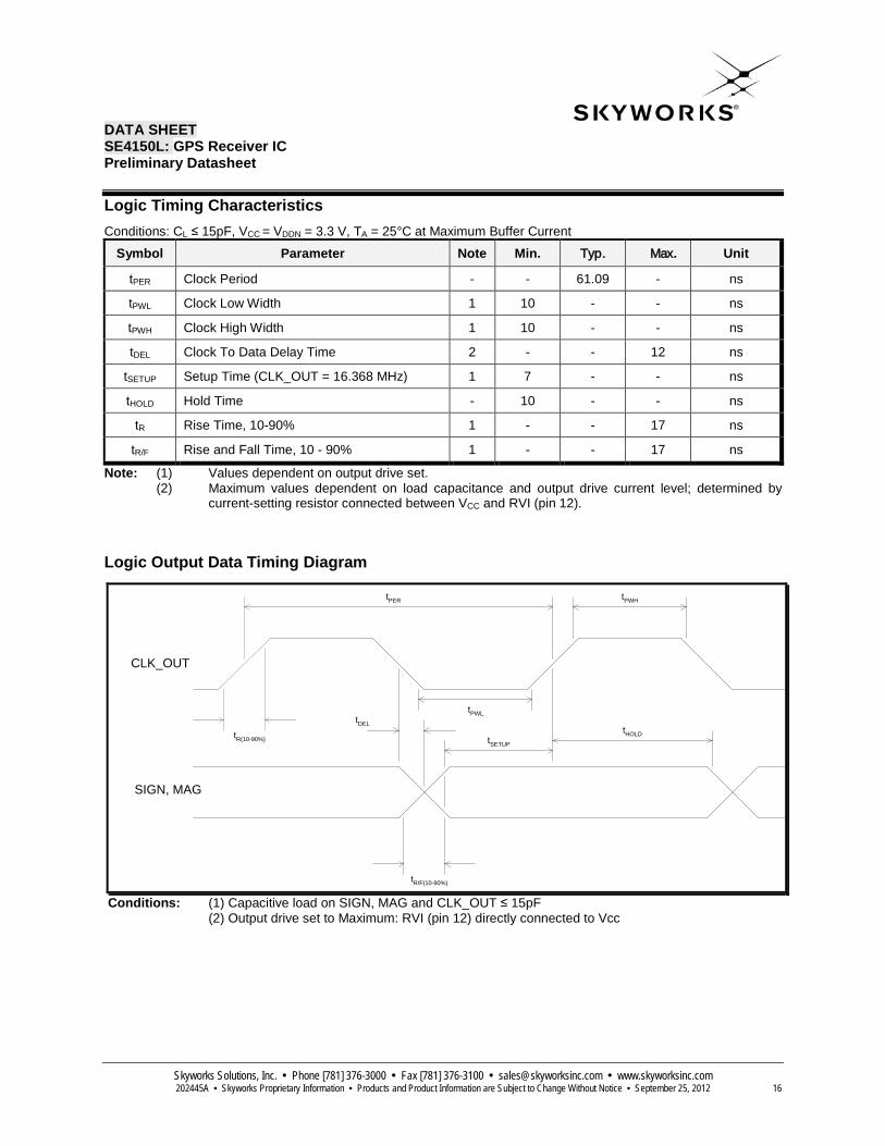
Logic Timing Characteristics Conditions: CL ≤ 15pF, VCC = VDDN = 3.3 V, TA = 25°C at Maximum Buffer Current
Symbol Parameter Note Min. Typ. Max. Unit
tPER Clock Period - - 61.09 - ns
tPWL Clock Low Width 1 10 - - ns
tPWH Clock High Width 1 10 - - ns
tDEL Clock To Data Delay Time 2 - - 12 ns
tSETUP Setup Time (CLK_OUT = 16.368 MHz) 1 7 - - ns
tHOLD Hold Time - 10 - - ns
tR Rise Time, 10-90% 1 - - 17 ns
tR/F Rise and Fall Time, 10 - 90% 1 - - 17 ns
Note: (1) Values dependent on output drive set. (2) Maximum values dependent on load capacitance and output drive current level; determined by
current-setting resistor connected between VCC and RVI (pin 12). Logic Output Data Timing Diagram
tR(10-90%)
tDEL
tSETUP
tHOLD
tR/F(10-90%)
tPER tPWH
tPWL
CLK_OUT
SIGN, MAG
Conditions: (1) Capacitive load on SIGN, MAG and CLK_OUT ≤ 15pF (2) Output drive set to Maximum: RVI (pin 12) directly connected to Vcc
DATA SHEET SE4150L: GPS Receiver IC Preliminary Datasheet
Skyworks Solutions, Inc. • Phone [781] 376-3000 • Fax [781] 376-3100 • [email protected] • www.skyworksinc.com 202445A • Skyworks Proprietary Information • Products and Product Information are Subject to Change Without Notice • September 25, 2012 17
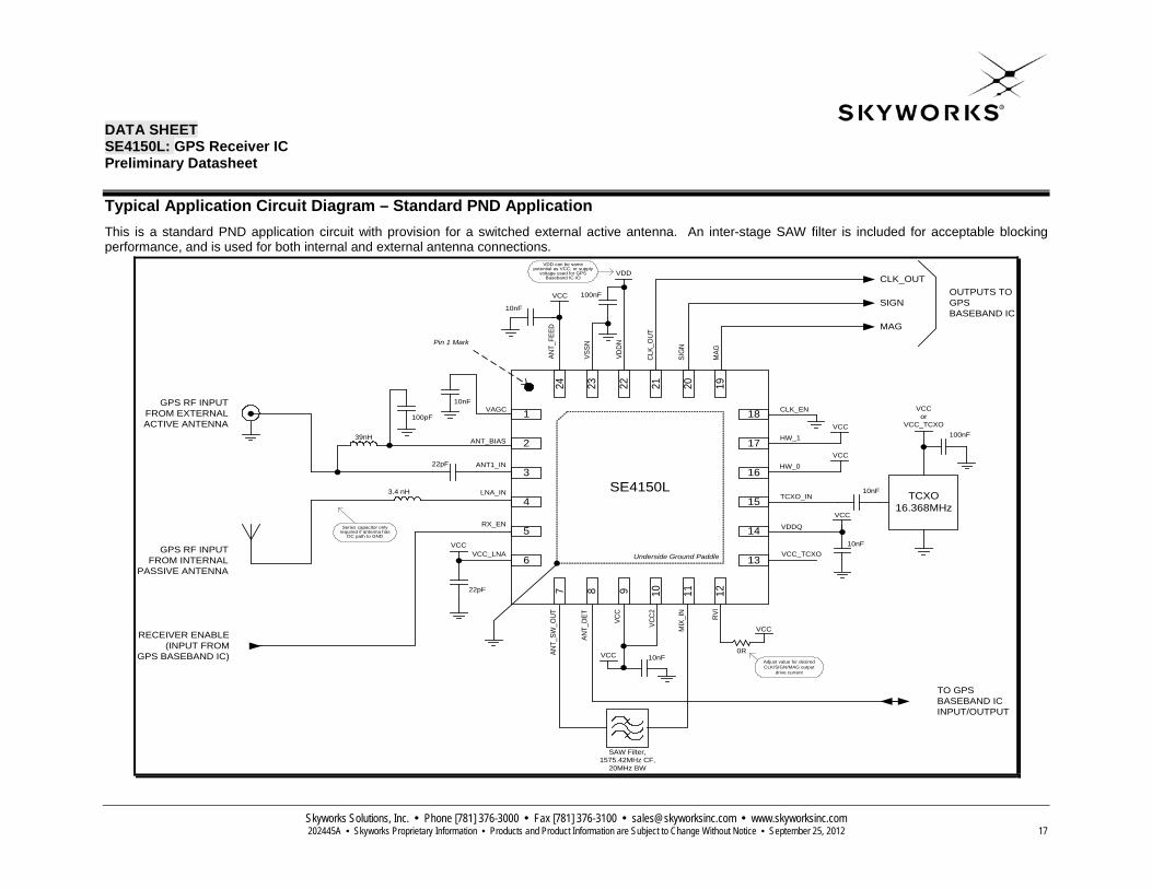
Typical Application Circuit Diagram – Standard PND Application
This is a standard PND application circuit with provision for a switched external active antenna. An inter-stage SAW filter is included for acceptable blocking performance, and is used for both internal and external antenna connections.
RVI
TCXO16.368MHz
VCC_TCXO
VDDQ
10nF
CLK_EN10nF
TCXO_IN
ANT1_IN
10nF
VCC
VCC
VCC
VDD
VCCor
VCC_TCXO
VCC_LNA
GPS RF INPUTFROM EXTERNALACTIVE ANTENNA
OUTPUTS TOGPSBASEBAND IC
SAW Filter,1575.42MHz CF,
20MHz BW
100nF
10nF
10nF
3.4 nH
1
2
3
4
5
6
18
17
16
15
14
1324 23 22 21 20 19
7 8 9 10 11 12
SE4150L
RECEIVER ENABLE(INPUT FROM
GPS BASEBAND IC)
Underside Ground Paddle
Pin 1 Mark
22pF
ANT_
SW_O
UT
VCC
VDDN
VAGC
ANT_BIAS
LNA_IN
100pF
39nH
22pF
GPS RF INPUTFROM INTERNAL
PASSIVE ANTENNA
RX_EN
VCC
VCC2
MIX
_IN
0R
VCC
ANT_
DET
100nFHW_1
HW_0
CLK_OUT
SIGN
MAG
CLK_
OUT
SIG
N
MAGVS
SN
ANT_
FEED
TO GPSBASEBAND ICINPUT/OUTPUT
Adjust value for desiredCLK/SIGN/MAG output
drive current
VDD can be samepotential as VCC, or supply
voltage used for GPSBaseband IC IO
Series capacitor onlyrequired if antenna has
DC path to GND
VCC
VCC
DATA SHEET SE4150L: GPS Receiver IC Preliminary Datasheet
Skyworks Solutions, Inc. • Phone [781] 376-3000 • Fax [781] 376-3100 • [email protected] • www.skyworksinc.com 202445A • Skyworks Proprietary Information • Products and Product Information are Subject to Change Without Notice • September 25, 2012 18
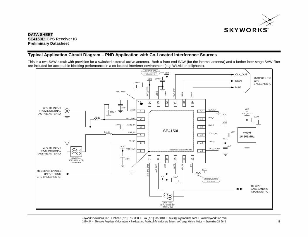
Typical Application Circuit Diagram – PND Application with Co-Located Interference Sources This is a two-SAW circuit with provision for a switched external active antenna. Both a front-end SAW (for the internal antenna) and a further inter-stage SAW filter are included for acceptable blocking performance in a co-located interferer environment (e.g. WLAN or cellphone).
RVI
TCXO16.368MHz
VCC_TCXO
VDDQ
10nF
CLK_EN10nF
TCXO_IN
ANT1_IN
10nF
VCC
VCC
VCC
VDD
VCCor
VCC_TCXO
VCC_LNA
GPS RF INPUTFROM EXTERNALACTIVE ANTENNA
OUTPUTS TOGPSBASEBAND IC
SAW Filter,1575.42MHz CF,
20MHz BW
100nF
10nF
10nF
3.4 nH
1
2
3
4
5
6
18
17
16
15
14
1324 23 22 21 20 19
7 8 9 10 11 12
SE4150L
RECEIVER ENABLE(INPUT FROM
GPS BASEBAND IC)
Underside Ground Paddle
Pin 1 Mark
22pF
ANT_
SW_O
UT
VCC
VDD
N
VAGC
ANT_BIAS
LNA_IN
100pF
39nH
22pF
GPS RF INPUTFROM INTERNAL
PASSIVE ANTENNA
RX_EN
VCC
VCC
2
MIX
_IN
0R
VCC
ANT_
DET
100nFHW_1
HW_0
CLK_OUT
SIGN
MAG
CLK
_OU
T
SIG
N
MAGVS
SN
ANT_
FEED
TO GPSBASEBAND ICINPUT/OUTPUT
Adjust value for desiredCLK/SIGN/MAG output
drive current
VDD can be samepotential as VCC, or supply
voltage used for GPSBaseband IC IO
VCC
VCC
SAW Filter,1575.42MHz CF,
20MHz BW
DATA SHEET SE4150L: GPS Receiver IC Preliminary Datasheet
Skyworks Solutions, Inc. • Phone [781] 376-3000 • Fax [781] 376-3100 • [email protected] • www.skyworksinc.com 202445A • Skyworks Proprietary Information • Products and Product Information are Subject to Change Without Notice • September 25, 2012 19
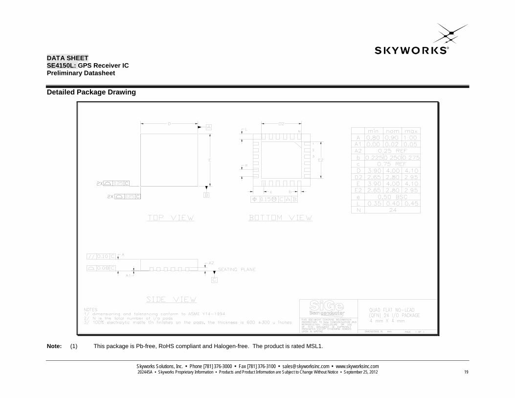
Detailed Package Drawing
Note: (1) This package is Pb-free, RoHS compliant and Halogen-free. The product is rated MSL1.
DATA SHEET SE4150L: GPS Receiver IC Preliminary Datasheet
Skyworks Solutions, Inc. • Phone [781] 376-3000 • Fax [781] 376-3100 • [email protected] • www.skyworksinc.com 202445A • Skyworks Proprietary Information • Products and Product Information are Subject to Change Without Notice • September 25, 2012 20
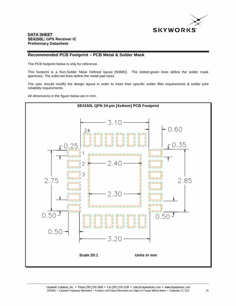
Recommended PCB Footprint – PCB Metal & Solder Mask
The PCB footprint below is only for reference. This footprint is a Non-Solder Mask Defined layout [NSMD]. The dotted-green lines define the solder mask apertures. The solid-red lines define the metal pad sizes. The user should modify the design layout in order to meet their specific solder fillet requirements & solder joint reliability requirements. All dimensions in the figure below are in mm.
SE4150L QFN 24-pin [4x4mm] PCB Footprint
Scale 20:1 Units in mm

DATA SHEET SE4150L: GPS Receiver IC Preliminary Datasheet
Skyworks Solutions, Inc. • Phone [781] 376-3000 • Fax [781] 376-3100 • [email protected] • www.skyworksinc.com 202445A • Skyworks Proprietary Information • Products and Product Information are Subject to Change Without Notice • September 25, 2012 21
Recommended PCB Footprint – Stencil Apertures Pattern
The stencil apertures design below is only for reference. It is based on a 6mil [0.15mm] stencil thickness with apertures oversized by 1mil [0.025mm] on the pad metal. The user should modify the design layout in order to meet their particular solder fillet & solder joint reliability requirements. All dimensions in the figure below are in mm.
SE4150L QFN 24-pin [4x4mm] PCB Footprint – Stencil Pattern
Scale 20:1 Units in mm

DATA SHEET SE4150L: GPS Receiver IC Preliminary Datasheet
Skyworks Solutions, Inc. • Phone [781] 376-3000 • Fax [781] 376-3100 • [email protected] • www.skyworksinc.com 202445A • Skyworks Proprietary Information • Products and Product Information are Subject to Change Without Notice • September 25, 2012 22
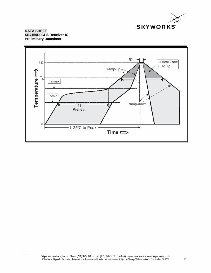
Recommended Reflow Temperature Profile
Profile Feature SnPb Eutectic Assembly Lead (Pb) Free Assembly
Average Ramp-up Rate (TL to TP) 3°C/s (max) 3°C/s (max)
Preheat
Temperature Min. (Tsmin) 100°C 150°C
Temperature Max. (Tsmax) 150°C 200°C
Time (Min. to Max) (ts) 60 - 120s 60 - 80s
Ramp Up
Tsmax to tL - 3°C/s (max)
Time 25°C to Peak Temperature 6 mins. (max) 8 mins. (max)
Reflow
Temperature (tL) 183°C 217°C
Time maintained above tL 60 - 150s 60 - 150s
Peak Temperature (tp) 240 ±5°C 260 +0/-5°C
Time Within 5°C of Actual Peak Temperature (tp)
10 - 30s 20 - 40s
Ramp-Down
Ramp-Down Rate 6°C/s (max) 6°C/s (max)
Reflow Profile (Reference JEDEC J-STD-020)
DATA SHEET SE4150L: GPS Receiver IC Preliminary Datasheet
Skyworks Solutions, Inc. • Phone [781] 376-3000 • Fax [781] 376-3100 • [email protected] • www.skyworksinc.com 202445A • Skyworks Proprietary Information • Products and Product Information are Subject to Change Without Notice • September 25, 2012 23
DATA SHEET SE4150L: GPS Receiver IC Preliminary Datasheet
Skyworks Solutions, Inc. • Phone [781] 376-3000 • Fax [781] 376-3100 • [email protected] • www.skyworksinc.com 202445A • Skyworks Proprietary Information • Products and Product Information are Subject to Change Without Notice • September 25, 2012 24
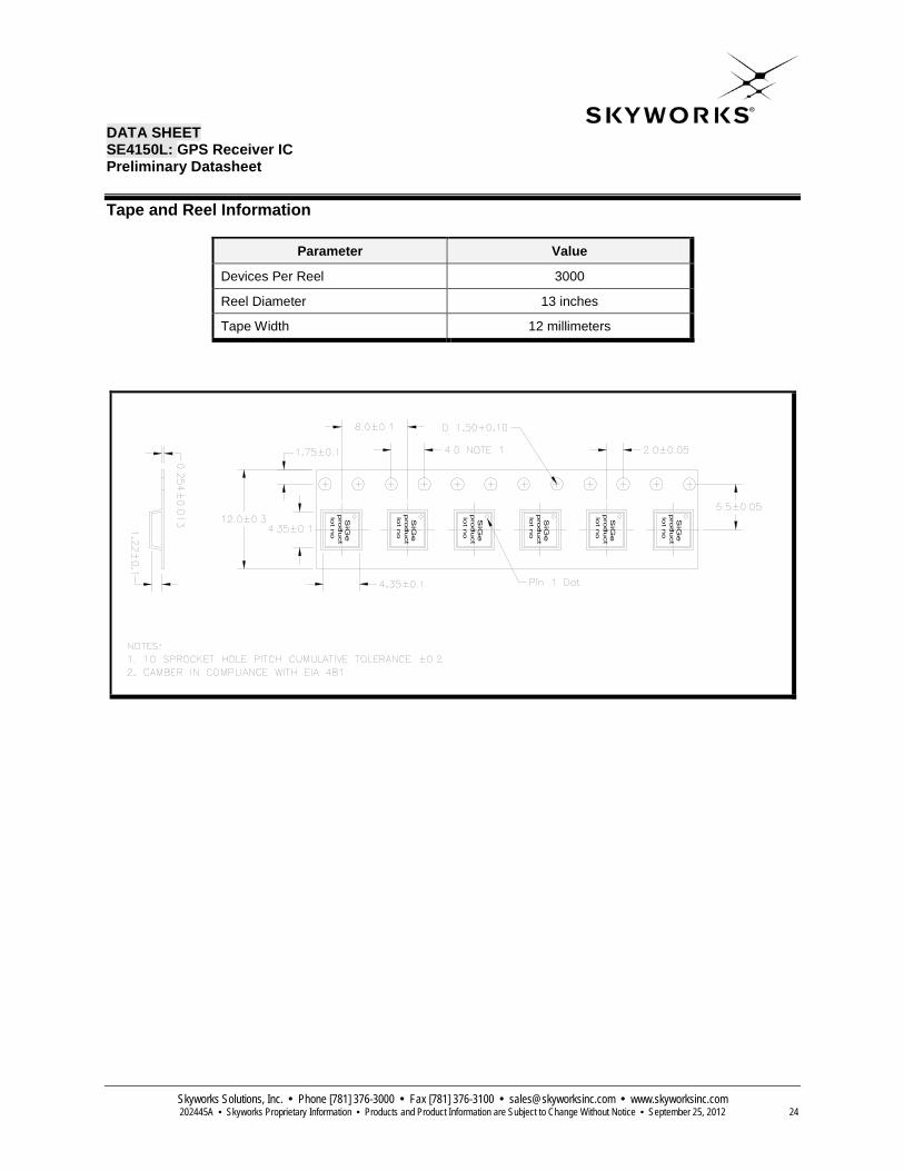
Tape and Reel Information
Parameter Value
Devices Per Reel 3000
Reel Diameter 13 inches
Tape Width 12 millimeters
DATA SHEET SE4150L: GPS Receiver IC Preliminary Datasheet
Skyworks Solutions, Inc. • Phone [781] 376-3000 • Fax [781] 376-3100 • [email protected] • www.skyworksinc.com 202445A • Skyworks Proprietary Information • Products and Product Information are Subject to Change Without Notice • September 25, 2012 25
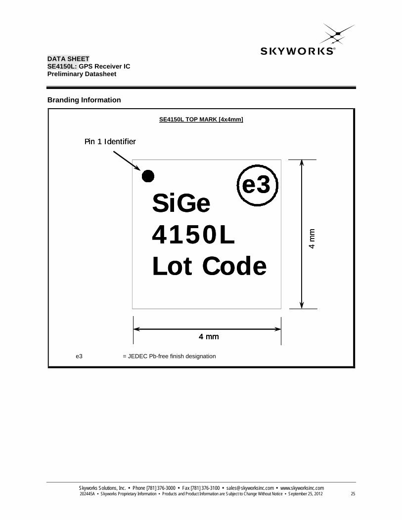
Branding Information
SE4150L TOP MARK [4x4mm]
SiGe4150LLot Code
e3
4 mm
4 m
m
Pin 1 Identifier
e3
4 mm
SiGe4150LLot Code
e3
4 mm
4 m
m
Pin 1 Identifier
e3
4 mm
e3 = JEDEC Pb-free finish designation
DATA SHEET SE4150L: GPS Receiver IC Preliminary Datasheet
Skyworks Solutions, Inc. • Phone [781] 376-3000 • Fax [781] 376-3100 • [email protected] • www.skyworksinc.com 202445A • Skyworks Proprietary Information • Products and Product Information are Subject to Change Without Notice • September 25, 2012 26
Copyright © 2012 Skyworks Solutions, Inc. All Rights Reserved.
Information in this document is provided in connection with Skyworks Solutions, Inc. (“Skyworks”) products or services. These materials, including the information contained herein, are provided by Skyworks as a service to its customers and may be used for informational purposes only by the customer. Skyworks assumes no responsibility for errors or omissions in these materials or the information contained herein. Skyworks may change its documentation, products, services, specifications or product descriptions at any time, without notice. Skyworks makes no commitment to update the materials or information and shall have no responsibility whatsoever for conflicts, incompatibilities, or other difficulties arising from any future changes.
No license, whether express, implied, by estoppel or otherwise, is granted to any intellectual property rights by this document. Skyworks assumes no liability for any materials, products or information provided hereunder, including the sale, distribution, reproduction or use of Skyworks products, information or materials, except as may be provided in Skyworks Terms and Conditions of Sale.
THE MATERIALS, PRODUCTS AND INFORMATION ARE PROVIDED “AS IS” WITHOUT WARRANTY OF ANY KIND, WHETHER EXPRESS, IMPLIED, STATUTORY, OR OTHERWISE, INCLUDING FITNESS FOR A PARTICULAR PURPOSE OR USE, MERCHANTABILITY, PERFORMANCE, QUALITY OR NON-INFRINGEMENT OF ANY INTELLECTUAL PROPERTY RIGHT; ALL SUCH WARRANTIES ARE HEREBY EXPRESSLY DISCLAIMED. SKYWORKS DOES NOT WARRANT THE ACCURACY OR COMPLETENESS OF THE INFORMATION, TEXT, GRAPHICS OR OTHER ITEMS CONTAINED WITHIN THESE MATERIALS. SKYWORKS SHALL NOT BE LIABLE FOR ANY DAMAGES, INCLUDING BUT NOT LIMITED TO ANY SPECIAL, INDIRECT, INCIDENTAL, STATUTORY, OR CONSEQUENTIAL DAMAGES, INCLUDING WITHOUT LIMITATION, LOST REVENUES OR LOST PROFITS THAT MAY RESULT FROM THE USE OF THE MATERIALS OR INFORMATION, WHETHER OR NOT THE RECIPIENT OF MATERIALS HAS BEEN ADVISED OF THE POSSIBILITY OF SUCH DAMAGE.
Skyworks products are not intended for use in medical, lifesaving or life-sustaining applications, or other equipment in which the failure of the Skyworks products could lead to personal injury, death, physical or environmental damage. Skyworks customers using or selling Skyworks products for use in such applications do so at their own risk and agree to fully indemnify Skyworks for any damages resulting from such improper use or sale.
Customers are responsible for their products and applications using Skyworks products, which may deviate from published specifications as a result of design defects, errors, or operation of products outside of published parameters or design specifications. Customers should include design and operating safeguards to minimize these and other risks. Skyworks assumes no liability for applications assistance, customer product design, or damage to any equipment resulting from the use of Skyworks products outside of stated published specifications or parameters.
Skyworks, the Skyworks symbol, and “Breakthrough Simplicity” are trademarks or registered trademarks of Skyworks Solutions, Inc., in the United States and other countries. Third-party brands and names are for identification purposes only, and are the property of their respective owners. Additional information, including relevant terms and conditions, posted at www.skyworksinc.com, are incorporated by reference.