Embed Size (px)
Citation preview

The University of MaineDigitalCommons@UMaine
Electronic Theses and Dissertations Fogler Library
Fall 12-2018
Application of Silicon Nanohair Textured p-nJunctions in a Photovoltaic DeviceMichael SmallUniversity of Maine, [email protected]
Follow this and additional works at: https://digitalcommons.library.umaine.edu/etd
Part of the Physics Commons, Power and Energy Commons, and the Semiconductor and OpticalMaterials Commons
This Open-Access Thesis is brought to you for free and open access by DigitalCommons@UMaine. It has been accepted for inclusion in ElectronicTheses and Dissertations by an authorized administrator of DigitalCommons@UMaine. For more information, please [email protected].
Recommended CitationSmall, Michael, "Application of Silicon Nanohair Textured p-n Junctions in a Photovoltaic Device" (2018). Electronic Theses andDissertations. 2949.https://digitalcommons.library.umaine.edu/etd/2949

Application of Silicon Nanohair Textured p-n Junctions in a
Photovoltaic Device
By
Michael D Small
B.S. Michigan Technological University, 2015
A Thesis
Submitted in Partial Fulfillment of the
Requirements for the Degree of
Master of Engineering
(in Engineering Physics)
The Graduate School
The University of Maine
December 2018
Advisory Committee:
Rosemary Smith, Professor of Electrical and Computer Engineering, Advisor
Scott Collins, Professor of Chemistry
Robert Meulenberg, Associate Professor of Physics

Application of Silicon Nanohair Textured p-n Junctions in a Photovoltaic
Device
By Michael D Small
Thesis Advisor: Dr. Rosemary Smith
An Abstract of the Thesis Presentedin Partial Fulfillment of the Requirements for the
Degree of Master of Engineering(in Engineering Physics)
December 2018
The goal of this project is to design and develop a fabrication process for a silicon photo-
voltaic device which incorporates a nanohair textured p-n junction. The silicon nanowires
are etched into a silicon wafer, comprising an epitaxial p-layer on n-substrate, via metal-
assisted chemical etching (MACE). The resulting nanowires contain p-n junctions that lie
along the length of the vertical nanowires. This construct has the potential to increase the
optical bandwidth of a silicon photovoltaic device by allowing a greater amount of short
wavelength light to reach the junction. In addition, the MACE method of nanofabrication
has the potential for decreasing the manufacturing complexity and related costs by elimi-
nating the need for photolithographic patterning.
The fabrication procedure is presented, along with material and morphological characteriza-
tion of the finished device. Device fabrication considerations include inter-nanowire material,
ohmic electrical contacts, and device passivation. Current vs voltage characteristics of the
nanowire device are presented and compared to its planar analog. Nanohair textured and pla-
nar device performance are compared under illumination of varying wavelength and intensity.

Nanohair textured devices are found to increase electron-hole pair generation under solar
simulated and blue light illumination with more significant gains found for blue light illu-
mination. This increased electron-hole pair generation is attributed to an increased amount
of short wavelength light reaching the p-n junction. However, nanohair textured devices are
found to have more significant surface recombination effects than planar devices that limit
the nanohair textured device efficiency under low intensity illumination. Both planar and
nanohair textured devices are found to have limited efficiency under intense illumination due
to series resistance effects.

ACKNOWLEDGMENTS
I would first like to thank my research advisor Dr. Rosemary Smith for her incredible sup-
port of my growth as a researcher. I appreciate so much the hours you spent answering
my many questions and helping overcome the numerous difficulties encountered throughout
this research. I am also so grateful for manner in which you mentored me; allowing me to
pursue this research as my own, but always knowing exactly when to provide a guiding hand.
I would like to thank the Laboratory for Surface Science and Technology and it’s members
for the partial financial support and the use of their resources. Specially, I would like to
thank Dr. Nuri Emanetoglu, Dr. Scott Collins, and Dr. Robert Meulenberg for the use
of their equipment, laboratories, and council. I would also like to thank Mike Call and Dr.
George Bernhardt for their many hours spent training and assisting me in the lab.
I would also like to thank Texas Instruments of South Portland Maine for generously pro-
viding me with the silicon wafers from which my devices were created.
Lastly, I would like to thank my friends and colleagues, Alex Khammang and Zachary Smith.
Thank you so much for always listening to me ramble about my problems in the lab and in
life and always being their to see me through them.
ii

TABLE OF CONTENTS
ACKNOWLEDGMENTS . . . . . . . . . . . . . . . . . . . . . . . . . . . . . . . ii
LIST OF FIGURES . . . . . . . . . . . . . . . . . . . . . . . . . . . . . . . . . . . vi
LIST OF TABLES . . . . . . . . . . . . . . . . . . . . . . . . . . . . . . . . . . . . xi
CHAPTER 1: INTRODUCTION . . . . . . . . . . . . . . . . . . . . . . . . . . 1
CHAPTER 2: BACKGROUND . . . . . . . . . . . . . . . . . . . . . . . . . . . 4
2.1 Photovoltaic Effect . . . . . . . . . . . . . . . . . . . . . . . . . . . . . . . . 4
2.2 p-n Junction . . . . . . . . . . . . . . . . . . . . . . . . . . . . . . . . . . . . 5
2.3 Anti-reflection and Light Trapping . . . . . . . . . . . . . . . . . . . . . . . 8
2.4 Nanohair Fabrication: Metal Assisted Chemical Etching . . . . . . . . . . . 10
2.5 Circuit Model . . . . . . . . . . . . . . . . . . . . . . . . . . . . . . . . . . . 13
2.6 Device Characteristics . . . . . . . . . . . . . . . . . . . . . . . . . . . . . . 15
2.7 Photovoltaic Characteristics . . . . . . . . . . . . . . . . . . . . . . . . . . . 18
CHAPTER 3: FABRICATION METHODS & RESULTS . . . . . . . . . . . 22
3.1 Nanohair Fabrication . . . . . . . . . . . . . . . . . . . . . . . . . . . . . . . 22
3.1.1 Process . . . . . . . . . . . . . . . . . . . . . . . . . . . . . . . . . . 22
3.2 Nanohair Backfill/Passivation . . . . . . . . . . . . . . . . . . . . . . . . . . 26
3.2.1 Process . . . . . . . . . . . . . . . . . . . . . . . . . . . . . . . . . . 26
iii

3.2.2 Process Development . . . . . . . . . . . . . . . . . . . . . . . . . . . 28
3.2.3 Surface Passivation via Thermal Oxidation . . . . . . . . . . . . . . . 34
3.3 Nanohair Tip Exposure . . . . . . . . . . . . . . . . . . . . . . . . . . . . . . 37
3.3.1 Process . . . . . . . . . . . . . . . . . . . . . . . . . . . . . . . . . . 37
3.3.2 Process Development . . . . . . . . . . . . . . . . . . . . . . . . . . . 39
3.4 Planar Device: Surface Etch-back . . . . . . . . . . . . . . . . . . . . . . . . 44
3.4.1 Process . . . . . . . . . . . . . . . . . . . . . . . . . . . . . . . . . . 44
3.4.2 Process Development . . . . . . . . . . . . . . . . . . . . . . . . . . . 46
3.5 Electrical Contacts . . . . . . . . . . . . . . . . . . . . . . . . . . . . . . . . 49
3.5.1 Process . . . . . . . . . . . . . . . . . . . . . . . . . . . . . . . . . . 49
3.5.2 Process Development . . . . . . . . . . . . . . . . . . . . . . . . . . . 53
CHAPTER 4: DEVICE CHARACTERIZATION METHODS & RESULTS 58
4.1 Material Characterization of Deposited Materials . . . . . . . . . . . . . . . 58
4.1.1 Ultraviolet-Visible Transmission Spectroscopy . . . . . . . . . . . . . 59
4.1.2 X-ray Photo-electron Spectroscopy . . . . . . . . . . . . . . . . . . . 60
4.1.3 Ultraviolet Photo-electron Spectroscopy . . . . . . . . . . . . . . . . 62
4.1.4 4-Point Conductivity . . . . . . . . . . . . . . . . . . . . . . . . . . . 64
4.2 Device Morphology . . . . . . . . . . . . . . . . . . . . . . . . . . . . . . . . 65
4.2.1 p-n Junction Area Loss in Silicon Nanohair Fabrication . . . . . . . . 65
4.2.2 Characterization of Lost Nanohair Height . . . . . . . . . . . . . . . 68
4.2.3 Device Cross-sections . . . . . . . . . . . . . . . . . . . . . . . . . . . 70
4.3 Photovoltaic Response Measurements . . . . . . . . . . . . . . . . . . . . . . 75
iv
4.3.1 Experimental Setup . . . . . . . . . . . . . . . . . . . . . . . . . . . . 75
4.3.2 Current/Voltage Characteristics: Dark . . . . . . . . . . . . . . . . . 77
4.3.3 Current/Voltage Characteristics: Solar Simulator . . . . . . . . . . . 80
4.3.4 Current/Voltage Measurements: Blue . . . . . . . . . . . . . . . . . . 84
4.3.5 Current/Voltage Characteristics: Ultraviolet . . . . . . . . . . . . . . 86
4.3.6 Summary of Device Photovoltaic Response . . . . . . . . . . . . . . . 89
CHAPTER 5: CONCLUSIONS . . . . . . . . . . . . . . . . . . . . . . . . . . . 93
CHAPTER 6: FUTURE WORK . . . . . . . . . . . . . . . . . . . . . . . . . . 98
BIBLIOGRAPHY . . . . . . . . . . . . . . . . . . . . . . . . . . . . . . . . . . . . 101
Appendix I: Nanohair Device Process Flow . . . . . . . . . . . . . . . . . . . . 104
Appendix II: Planar Device Process Flow . . . . . . . . . . . . . . . . . . . . . 108
Appendix III: Device Schematics . . . . . . . . . . . . . . . . . . . . . . . . . . 112
Appendix IV: Stock Solutions . . . . . . . . . . . . . . . . . . . . . . . . . . . . 114
Appendix V: Equipment . . . . . . . . . . . . . . . . . . . . . . . . . . . . . . . . 115
Appendix VI: Silicon Wafer Characteristics . . . . . . . . . . . . . . . . . . . . 116
Appendix VII: Device Performance Distributions . . . . . . . . . . . . . . . . 119
BIOGRAPHY OF THE AUTHOR . . . . . . . . . . . . . . . . . . . . . . . . . 122
v

LIST OF FIGURES
1.1 Cross-sectional schematic of the proposed nanohair textured device . . . . . 2
2.2 Fraction of light transmitted in Silicon as a function of wavelength of light
and depth in material. Calculated from Filmetrics data . . . . . . . . . . . . 7
2.3 (a) Absorption depth of light in a planar photovoltaic device compared to (b)
the absorption depth of light in a nanohair textured photovoltaic device . . . 8
2.4 (a) Paths of reflected light for a planar photovoltaic device compared to (b)
the paths of reflected light for a nanohair textured photovoltaic device . . . . 9
2.5 Schematic of silver nanoparticles burrowing into a silicon surface during a
metal assisted chemical etch . . . . . . . . . . . . . . . . . . . . . . . . . . . 11
2.6 45 degree scanning electron microscope cross-section of typical nanohair array
produced via MACE method . . . . . . . . . . . . . . . . . . . . . . . . . . . 12
2.7 Circuit model of a photovoltaic device . . . . . . . . . . . . . . . . . . . . . 13
2.8 Regression fit of the saturation region (left) and recombination region (right)
for a typical planar device made during this research . . . . . . . . . . . . . 16
2.9 Regression fit of the series resistance dominated region (left) and shunt resis-
tance dominated region (right) of a typical diode . . . . . . . . . . . . . . . . 17
2.10 Typical illuminated characteristics of a photovoltaic device . . . . . . . . . . 19
3.11 Top view (a) and cross-section view (b) of the nanohair textured device fol-
lowing the fabrication of the silicon nanohairs . . . . . . . . . . . . . . . . . 23
vi

3.12 45 degree SEM cross-section of typical nanohair array fabricated via the
MACE process . . . . . . . . . . . . . . . . . . . . . . . . . . . . . . . . . . 25
3.13 Top view (a) and cross-section view (b) of the nanohair textured device fol-
lowing the backfill of the silicon nanohair textured surface . . . . . . . . . . 27
3.14 800nm of PECVD silicon oxide deposited on silicon nanohairs . . . . . . . . 30
3.15 Titanium nanoparticles deposited on silicon nanohairs via solution deposition 30
3.16 JR White epoxy deposited on silicon nanohairs via solvent casting . . . . . . 31
3.17 Parylene deposited on silicon nanohairs via vapor deposition . . . . . . . . . 31
3.18 Atomic layer deposition aluminum oxide deposited on silicon nanohairs . . . 32
3.19 Measured and fitted thermal oxidation characteristics of p-type epitaxial silicon 35
3.20 45 degree SEM cross-section of silicon nanohairs thermally oxidized in air at
800C for 15min . . . . . . . . . . . . . . . . . . . . . . . . . . . . . . . . . . 36
3.21 Top view (a) and cross-section view (b) of the nanohair textured device fol-
lowing the exposure of the nanohair tips . . . . . . . . . . . . . . . . . . . . 38
3.22 Plot of ALD aluminum oxide thickness as measured by ellipsometer for varying
time in 5% HF solution . . . . . . . . . . . . . . . . . . . . . . . . . . . . . . 40
3.23 45 degree SEM cross-section of aluminum oxide back-filled nanohairs before
hydroflouric acid solution back-etch . . . . . . . . . . . . . . . . . . . . . . . 41
3.24 45 degree SEM cross-section of aluminum oxide back-filled nanohairs after
hydroflouric acid solution back-etch . . . . . . . . . . . . . . . . . . . . . . . 42
3.25 Top view (a) and cross-section view (b) of the planar device following the
etch-back of the silicon surface . . . . . . . . . . . . . . . . . . . . . . . . . . 45
3.26 Depth of silicon lost in KOH etch as measured by optical profilometer . . . . 48
vii

3.27 Top view (a) and cross-section view (b) of the nanohair textured device fol-
lowing the attachment of electrical contacts . . . . . . . . . . . . . . . . . . 50
3.28 Top view (a) and cross-section view (b) of the planar device following the
attachment of electrical contacts . . . . . . . . . . . . . . . . . . . . . . . . . 51
4.29 Transmission spectrum of magnetron sputtered indium tin oxide and atomic
layer deposition aluminum oxide films . . . . . . . . . . . . . . . . . . . . . . 59
4.30 Measured characteristic energy lines and material composition of atomic layer
deposition aluminum oxide . . . . . . . . . . . . . . . . . . . . . . . . . . . . 61
4.31 Measured characteristic energy lines and material composition of annealed
magnetron sputtered indium tin oxide . . . . . . . . . . . . . . . . . . . . . . 61
4.32 Measured photo-electron energy spectrum of ultraviolet illuminated indium
tin oxide . . . . . . . . . . . . . . . . . . . . . . . . . . . . . . . . . . . . . . 63
4.33 Representative SEM top-view image of a silicon nanohair textured surface . 66
4.34 Intensity map of imaged nanohair surface (shown in green) for various applied
threshold values . . . . . . . . . . . . . . . . . . . . . . . . . . . . . . . . . . 68
4.35 Schematic cross-section of the device profile over which the lost silicon height
was measured . . . . . . . . . . . . . . . . . . . . . . . . . . . . . . . . . . . 69
4.36 45 degree SEM cross-section of a nanohair textured device representative of
the upper performance extreme . . . . . . . . . . . . . . . . . . . . . . . . . 71
4.37 45 degree SEM cross-section of a nanohair textured device representative of
the lower performance extreme . . . . . . . . . . . . . . . . . . . . . . . . . . 72
4.38 Schematic cross-section of the measured nanohair texture device morphology 73
viii
4.39 Schematic of the setup used to measure the diode characteristics and photo-
voltaic response of the nanohair textured and planar devices . . . . . . . . . 75
4.40 Normalized light source spectra used to stimulated nanohair textured and
planar devices during photovoltaic response testing . . . . . . . . . . . . . . 76
4.41 Non-illuminated current/voltage relationships for representative nanohair and
planar devices . . . . . . . . . . . . . . . . . . . . . . . . . . . . . . . . . . . 77
4.42 Current/voltage relationships for representative nanohair and planar devices
under 680 Wm2 AM 1.5 solar simulated illumination . . . . . . . . . . . . . . . 80
4.43 Current/voltage relationships for representative nanohair and planar devices
under 13 Wm2 AM 1.5 solar simulated illumination . . . . . . . . . . . . . . . . 83
4.44 Current/voltage relationships for representative nanohair and planar devices
under blue laser illumination . . . . . . . . . . . . . . . . . . . . . . . . . . . 85
4.45 Current/voltage relationships for representative nanohair and planar devices
under ultra-violet illumination . . . . . . . . . . . . . . . . . . . . . . . . . . 87
5.46 Non-illuminated current/voltage characteristics and photo-response of top
performing nanohair textured device under 13W/m2 solar simulated, blue
laser, and ultraviolet illumination . . . . . . . . . . . . . . . . . . . . . . . . 94
5.47 Non-illuminated current/voltage characteristics and photo-response of top
performing nanohair textured device under 860W/m2 solar simulated illu-
mination . . . . . . . . . . . . . . . . . . . . . . . . . . . . . . . . . . . . . . 94
6.48 (a) Side view, (b) top view, and (c) cross-section of nanohair textured photo-
voltaic device . . . . . . . . . . . . . . . . . . . . . . . . . . . . . . . . . . . 112
6.49 (a) Side view, (b) top view, and (c) cross-section of planar photovoltaic device 113
ix

6.50 Dopant concentration profile across the p-n junction of the wafer used in
device fabrication . . . . . . . . . . . . . . . . . . . . . . . . . . . . . . . . . 117
6.51 Dopant concentration profile of the n+ silicon cap of the wafer used in device
fabrication . . . . . . . . . . . . . . . . . . . . . . . . . . . . . . . . . . . . . 118
x

LIST OF TABLES
4.1 Fitted circuit model values of 13 planar and 15 nanohair devices . . . . . . . . . . . . 78
4.2 Fitted photovoltaic response values of 13 planar and 15 nanohair devices under 680 W
m2 AM
1.5 solar simulator illumination . . . . . . . . . . . . . . . . . . . . . . . . . . . . 81
4.3 Fitted photovoltaic response values of 12 planar and 11 nanohair devices under 13 W
m2 AM
1.5 solar simulator illumination . . . . . . . . . . . . . . . . . . . . . . . . . . . . 83
4.4 Fitted photovoltaic response values of planar and nanohair devices under blue diode laser
illumination . . . . . . . . . . . . . . . . . . . . . . . . . . . . . . . . . . . . . 85
4.5 Fitted photovoltaic response values of 10 planar and 15 nanohair devices under ultraviolet
lamp illumination . . . . . . . . . . . . . . . . . . . . . . . . . . . . . . . . . . 87
5.6 Fitted photovoltaic response values of the top performing nanohair textured device under
various illumination sources . . . . . . . . . . . . . . . . . . . . . . . . . . . . . . 95
xi

CHAPTER 1: INTRODUCTION
Silicon nanohairs (or nanowires) have recently been a subject of research concerning their
application in photovoltaic devices due to their electrical, material, and optical properties.
Several methods for industry viable large scale fabrication of silicon nanohair arrays has
been presented by various research groups [1,2]. These scalable production methods come
with the added benefit of silicon already being a widely used semiconductor material for
the production of photovoltaic devices. Additionally, studies have demonstrated that the
3D geometry of silicon nanohairs results in superior light trapping over planar surfaces [1,3].
Further studies have investigated methods for incorporating silicon nanohairs into devices
including radial silicon nanowire p-n junctions and silicon nanowire textured surfaces and
have found comparable or increased performance.
The goal of this project is to design and develop a fabrication process for a silicon photo-
voltaic device which incorporates a nanowire textured p-n junctions. Shown in Figure 1.1,
the morphology of this design is such that the p-n junction of the photovoltaic devices lies
along the length of an array of silicon nanohairs. Silicon nanohairs are fabricated via a
metal enhanced chemical etching method as it has the potential to be a commercially viable
method of production. Resulting nanohairs are such that the lengths are on the order of mi-
crons with diameters on the order of hundreds of nanometers. Additional device fabrication
considerations include inter-nanowire material, ohmic electrical contacts, and device passiva-
tion. Following the completion of the devices, differences in performance between nanohair
textured and planar devices under light sources of varying intensity and wavelength were
1

investigated.
Figure 1.1: Cross-sectional schematic of the proposed nanohair textured device
The organization of this thesis is summarized as follows. Chapter 2 contains the theory
behind photovoltaic devices, background concerning the fabrication of silicon nanohairs, and
the circuit model used for the characterization of the devices. The photovoltaic effect is pre-
sented along with the theory of the p-n junction. Then, these concepts are used to present
principles governing the performance of photovoltaic devices. The theory behind the metal
enhanced chemical etching process for silicon nanohair fabrication is presented in addition
to optical effects of nanohair texturing. Finally, a circuit model of the photovoltaic device
is presented which will be used to analyze the results of photovoltaic response measurements.
Chapter 3 contains the experimental methods and results of photovoltaic device fabrication.
Fabrication steps are presented chronological to the process flow with each section detailing
the experimental process used to optimize the method used for that step. The fabrication
2

steps discussed include nanohair fabrication, nanohair backfill, nanohair tip exposure, planar
surface etch-back, and electrical contacts. Full details of the final process flow are given in
Appendix I and II.
Chapter 4 details the material, morphological, and performance characteristics of the photo-
voltaic devices. Deposited film characteristics such as UV-visible transmission, conductivity,
and work function are reported. Various aspects of device morphology are also reported,
including the measurement of p-n junction area loss in nanohair textured devices, nanohair
height and distribution, film thickness. Finally, the diode characteristics of the finished
nanohair textured and planar devices are reported for non-illuminated and illuminated con-
ditions, using light sources of various wavelength and intensity.
3

CHAPTER 2: BACKGROUND
2.1 Photovoltaic Effect
Photons incident on a material can be absorbed or propagate through the material depend-
ing upon the energy of the photons and the bandgap of the material. For photon energies
less than the bandgap, light is not readily absorbed and the material appears transparent.
However, photons with energy exceeding that of the bandgap can interact with valance elec-
trons; imparting enough energy to elevate them into a conduction band state. [4] This is
known as the photoabsorption effect.
The photoabsorption effect results in an electron in a conduction band state in which it
can more freely move throughout that material under stimulus of and electric field. This
transition between states also results in a vacant state left in the valance band, referred to
as a hole. This hole can also move relatively freely under the stimulus of an electric field;
however it does so as a positively charged particle. [5]
As electrons and holes are of opposite charge, they will attract each other and in proximity
they will annihilate each other; an effect called recombination. Therefore in order to make
use of the electron-hole pairs created by photoabsorption, they must be separated by an
electric field. This is readily done through the use of a p-n junction, producing what is
known as the photovoltaic effect.
4
2.2 p-n Junction
A p-n junction is the metalurgical boundary between a p-type and an n-type semiconductor.
A semiconductor is made n-type or p-type through the addition of donor or acceptor impurity
atoms, respectively. The addition of impurities into the semiconductor result in additional
electrons for donor impurities and holes for acceptor impurities. When a p-n junction is
created, excess electrons present in the n-type semiconductor diffuse across the metallurgical
boundary and into the excess hole states of the p-type semiconductor. The transfer of just
a small amount of charge at the junction results in a built-in electric field, which opposes
further diffusion, establishing equilibrium. Assuming the concentration of acceptor states,
Na, and donor states, Nd, are uniform on each respective side of the junction, the potential,
Vbi, across the p-n junction, is given by the following equation: [5]
Vbi =kT
eln(
NaNd
n2i
) (2.1)
The movement of electrons and holes from either side of the p-n junction results in a region
in which there are no free charge carriers, called a depletion region. It is across this region
that the built in potential exists. The width of the region can be found calculated using the
equation below. [5]
W = [2ǫsVbi
e(Na +Nd
NaNd)]1/2 (2.2)
Electron-hole pairs produced in this region via the photovoltaic effect are immediately under
the influence of the built-in potential. Electrons flow in the direction opposite to the electric
field sign, towards the n-type region and holes travel with the electric field sign, to the p-type
5
region. This separation of the charges results in the production of an electric current that
can be delivered to an external load, producing power (current x voltage).
The magnitude of the current produced by a photovoltaic device is directly related to the
electron-hole pair generation rate, G(λ, x). The generation rate is defined as the number of
electron-hole pairs generated per incident photon at each wavelength, λ, and is described by
the following equation: [6]
G(λ, x) = α(λ)F (λ)(1− R(λ))exp(−α(λ)x) (2.3)
Where; α(λ) is the absorption coefficient
F (λ) is the number of incident photons per area per time
R(λ) is the fraction of photons reflected from the surface
Absorption of photon energy in a semiconductor means that electron-hole pairs are gen-
erated. Here, the term exp(−α(λ)x) gives the fraction of incident light of wavelength, λ,
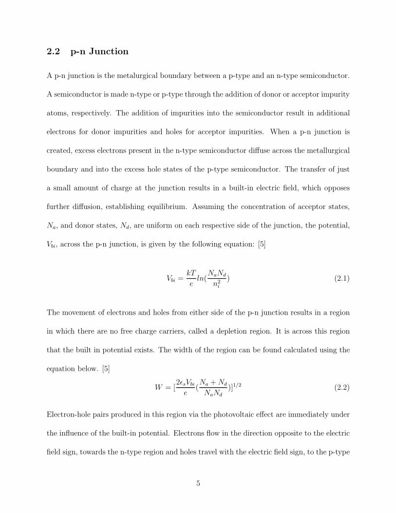
transmitted at depth, x. Using absorption coefficient data from Filmetrics [7], the rela-
tionship between the fraction of light absorbed, wavelength, and depth can be calculated
and plotted, as shown in Figure 2.2. Here the transmission curves deviate slightly from the
theoretical smooth exponential behavior as a result of variation in the measured absorption
coefficient.
6

200 300 400 500 600 700 800
Wavelength (nm)
0
5
10
15
20D
epth
(um
)
Wavelength and Depth Dependence of the Fraction of
Light Transmitted in (100) Silicon
0.1
0.3
0.5
0.7
0.9
Figure 2.2: Fraction of light transmitted in Silicon as a function of wavelength of light and depth inmaterial. Calculated from Filmetrics data
As shown in Figure 2.2, the depth at which light is absorbed in silicon depends very greatly
upon its wavelength. For wavelengths shorter than 500nm, light is very heavily absorbed
over depths shorter than half a micron. This is detrimental to the bandwidth of Silicon
photovoltaics as typically there is some depth of silicon above the depletion region, which
the light must first travel through by diffusion. Light absorbed in this layer of silicon cannot
contribute to the current output of the photovoltaic device if the generated carriers recom-
bine before reaching the depletion region, as electron-hole pair separation can only occur
within the depletion region.
Another significant impact on electron-hole pair generation rate is the reflectivity of the
device surface. Incident photons that are reflected by the device surface will not be ab-
sorbed and generate electron-hole pairs. Two common methods for reducing reflectivity are
7

texturing of the device surface or use of an anti-reflection coating. [6]
2.3 Anti-reflection and Light Trapping
An increase in shorter wavelength light collection over planar devices is predicted as a result
of the exposed p/n junction along the sides of the nanowires. Figure 2.3 demonstrates a
case in which a given frequency of light may be absorbed outside of the depletion layer for a
planar device, but may be absorbed inside the depletion layer for a nanohair textured device.
The total distance traveled through silicon is the same for each of the devices. However, the
density of silicon is less in the nanohair textured device; allowing for the light to penetrate
more deeply into the device.
Figure 2.3: (a) Absorption depth of light in a planar photovoltaic device compared to (b) the absorptiondepth of light in a nanohair textured photovoltaic device
An additional increase in efficiency over planar devices is predicted due to light channeling
between nanohairs. Figure 2.4 demonstrates possible light ray paths for reflected light for
planar and nanohair textured devices. In the case of the planar devices, light can only be
reflected away from the device surface, preventing it from ever being absorbed. A nanohair
8

textured device may result in greater light absorbed due to possible reflected ray paths di-
rected towards the depletion region within the space between nanohairs, which is not possible
in the case of a planar device. Additionally, the vertical structure of the nanohairs allows
for light rays to be reflected back towards the depletion region for all rays with a directional
component tangent to the device surface.
Figure 2.4: (a) Paths of reflected light for a planar photovoltaic device compared to (b) the paths ofreflected light for a nanohair textured photovoltaic device
9

2.4 Nanohair Fabrication: Metal Assisted Chemical Etching
Nanohair texturing of the silicon p-n junction is accomplished through Metal Assisted Chem-
ical Etching (MACE). This technique has recently shown great potential as a low cost option
for controllable anisotropic etching of silicon as this method can be done in a chemical lab
without expensive equipment. MACE has also been demonstrated as an effective method
for the fabrication of silicon nanohairs of varying length and aspect ratio. [5,6]
The specific MACE method used in this research consisted of two steps; the deposition of
silver nanoparticles followed by a silicon etch. Silver nanoparticles are deposited onto the
silicon surface by submerging the silicon in a solution of silver nitrate and hydroflouric acid.
Following this deposition, the silver coated silicon surface is then submerged in an etching
solution composed of hydrogen peroxide and hydroflouric acid. The silver nanoparticles en-
hance the oxidation rate of the adjacent silicon in the peroxide + HF solution. The silicon
oxide is then etched away by the hydroflouric acid in the solution, resulting in more rapid
etching of silicon at sites of silver nanoparticles. [8,9] The concentrations of the solutions
used and additional process details concerning the nanohair fabrication process are given in
Chapter 2 as well as in the Appendix I. Shown in Figure 2.5 is a schematic of the etching
process.
10
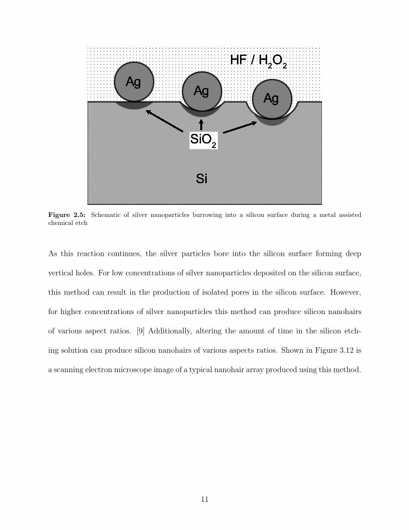
Figure 2.5: Schematic of silver nanoparticles burrowing into a silicon surface during a metal assistedchemical etch
As this reaction continues, the silver particles bore into the silicon surface forming deep
vertical holes. For low concentrations of silver nanoparticles deposited on the silicon surface,
this method can result in the production of isolated pores in the silicon surface. However,
for higher concentrations of silver nanoparticles this method can produce silicon nanohairs
of various aspect ratios. [9] Additionally, altering the amount of time in the silicon etch-
ing solution can produce silicon nanohairs of various aspects ratios. Shown in Figure 3.12 is
a scanning electron microscope image of a typical nanohair array produced using this method.
11

Figure 2.6: 45 degree scanning electron microscope cross-section of typical nanohair array produced viaMACE method
12

2.5 Circuit Model
The circuit model of the nanohair textured device is given in Figure 1. The model includes
the diode in series with a resistor to model an ideal p-n junction with some series resistance,
Rs, due to the bulk silicon and contacts. A second resistor, Rsh, is added in parallel to the
primary diode in order to account for a leakage current path. This parallel resistance is
referred to as the shunt resistance. [4]
Figure 2.7: Circuit model of a photovoltaic device
Using this model, the current-voltage characteristics of the circuit are;
I(V ) = Ir(eq(V−I(V )Rs)/(nrkT )
− 1) + Is(eq(V−I(V )Rs)/(nskT )
− 1) +(V − I(V )Rs)
Rsh(2.4)
13

Where; Is is the diode saturation current
Ir is the diode recombination current
nr is the recombination region ideality factor, (≈ 2)
ns is the saturation region ideality factor, (≈ 1)
Rs is the series resistance
Rsh is the shunt resistance
I(V ) is the current through the diode
V is the applied voltage
Is, Ir, ns, nr, Rs, and Rsh are all values that can have a significant effect on the device
performance and are dependent upon device design parameters. For this reason it is essential
that each of these variables be reliably and consistently measured for a given device design.
14

2.6 Device Characteristics
The circuit model includes effects that can result in device behavior which deviates from
that of an ideal diode. These effects are leakage, recombination, and series resistance and
each can be found to dominate device performance over certain ranges of applied voltage
and current output. The influence of these effects can be found in their corresponding terms
in Equation 2.4. Simplifying Equation 2.4 in terms of these effects yields;
I(V ) = Irecombination + Iideal + Ileakage (2.5)
Where; Irecombination = Ir(eq(V−I(V )Rs)/nrkT − 1)
Iideal = Is(eq(V−I(V )Rs)/nskT − 1)
Ileakage = (V − I(V )Rs)/Rsh
Here the device current, I(V ), is seen to be a function of the ideal diode current, Iideal, the
current produced via the recombination of electron-hole pairs, Irecombination, and the current
produced via charge carriers traveling around the p-n junction via a shunt path, Ileakage.
The effects leakage via the shunt resistance path can be expected to be found for very small
forward biases (approximately 0-0.1V) as Ileakage will be significantly larger that either Iideal
or Irecombination in this voltage range. The effects of recombination can be expected to be
found for low to mid forward biases (approximately 0-0.5V), as the exponential nature of
Irecombination will increase it’s value above that of Ileakage and Iideal. The effects of recom-
bination will always be found in a lower forward bias than the ideal diode characteristics
15
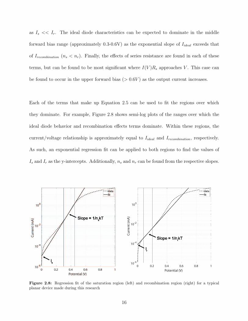
as Is << Ir. The ideal diode characteristics can be expected to dominate in the middle
forward bias range (approximately 0.3-0.6V) as the exponential slope of Iideal exceeds that
of Irecombination (ns < nr). Finally, the effects of series resistance are found in each of these
terms, but can be found to be most significant where I(V )Rs approaches V . This case can
be found to occur in the upper forward bias (> 0.6V ) as the output current increases.
Each of the terms that make up Equation 2.5 can be used to fit the regions over which
they dominate. For example, Figure 2.8 shows semi-log plots of the ranges over which the
ideal diode behavior and recombination effects terms dominate. Within these regions, the
current/voltage relationship is approximately equal to Iideal and Irecombination, respectively.
As such, an exponential regression fit can be applied to both regions to find the values of
Is and Ir as the y-intercepts. Additionally, ns and nr can be found from the respective slopes.
Figure 2.8: Regression fit of the saturation region (left) and recombination region (right) for a typicalplanar device made during this research
16

Similarly, Figure 2.9 shows the regions over which leakage and series resistance effects dom-
inate. Within these regions, the current/voltage relationship can be found to be approxi-
mately linear. Fitting a line to these regions yields slopes equal to the inverse of the series,
Rs, and shunt resistance, Rsh, respectively.
Figure 2.9: Regression fit of the series resistance dominated region (left) and shunt resistance dominatedregion (right) of a typical diode
17
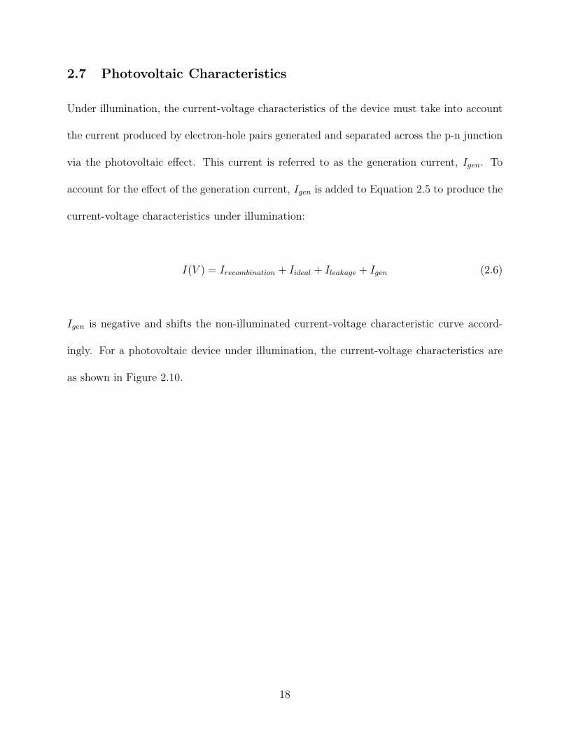
2.7 Photovoltaic Characteristics
Under illumination, the current-voltage characteristics of the device must take into account
the current produced by electron-hole pairs generated and separated across the p-n junction
via the photovoltaic effect. This current is referred to as the generation current, Igen. To
account for the effect of the generation current, Igen is added to Equation 2.5 to produce the
current-voltage characteristics under illumination:
I(V ) = Irecombination + Iideal + Ileakage + Igen (2.6)
Igen is negative and shifts the non-illuminated current-voltage characteristic curve accord-
ingly. For a photovoltaic device under illumination, the current-voltage characteristics are
as shown in Figure 2.10.
18
Figure 2.10: Typical illuminated characteristics of a photovoltaic device
Of special interest are the two limiting cases of V = 0 and I = 0. The current measured at
V = 0 is called the short circuit current, Isc, and the voltage measured at I = 0 is called the
open circuit voltage, Voc. The product of these values gives the maximum theoretical power
that can be produced by the photovoltaic device, Pmax.
Pmax = Isc × Voc (2.7)
The total power produced by the photovoltaic device, Ptotal is found by calculating the area
above the current-voltage curve where V > 0 and I < 0. The ratio between the total power
and the maximum theoretical power is referred to as the fill factor, FF , of the device. The
19

fill factor can range in value from 0 to ≈ 1, with lower fill factors indicating inefficiencies in
the device resulting from recombination or series resistance effects.
20

REFERENCES
1. Zhipeng Huang, Nadine Geyer, et.al., ”Metal-Assisted Chemical Etching of Silicon: A
Review”, Advanced Materials, 23, 285-308, 2011.
2. Kui-Qing Peng, Shuit-Tong Lee, ”Silicon Nanowires for Photovoltaic Solar Energy
Conversion”, Advanced Materials, 27, 198-215, 2011.
3. Junshuai Li, HongYu Yu, ”Aligned Si nanowire-based solar cells”, Nanoscale, 3, 4888,
2011.
4. S. M. Sze, Physics of Semiconductor Devices, John Wiley & Sons Inc., Hoboken, New
Jersey, 2007, pgs. 719-725.
5. Donald A. Neamen, Semiconductor Physics and Devices, McGraw-Hill, New York, New
York, 2003, pgs. 76, 238-250.
6. Edward S. Yang, Fundamentals of Semiconductor Devices, McGraw-Hill Book Com-
pany, 1978, pgs. 147-160.
7. Filmetrics, Refractive Index of Silicon, Si, https://www.filmetrics.com/refractive-index-
database/Si/Silicon
8. Zachary R. Smith, Rosemary L. Smith, Scott D. Collins, ”Mechanism of Nanowire
Formation in Metal Assisted Chemical Etching”, Electrochimica Acta, 92, 139-147,
2013.
21

CHAPTER 3: FABRICATION METHODS &
RESULTS
3.1 Nanohair Fabrication
3.1.1 Process
Device fabrication began with the nanohair texturing of p-type silicon surface. Shown in
Figure 3.11 is a schematic of the device following this process. Nanohairs of length Lhair were
etched into a circular area in the center of a p/n/n+ silicon chip. This process also removes
a length of silicon above the nanohairs, tlost, which results in the tips of the nanohairs being
recessed from the original silicon surface. Characterization of the nanohair length and the
length of silicon lost from the nanohair tips is reported in Chapter 4.
22

Figure 3.11: Top view (a) and cross-section view (b) of the nanohair textured device following the fabri-cation of the silicon nanohairs
Individual devices were first prepared for the nanohair etching process by dicing a silicon
wafer and masking the silicon for selective nanohair etching. A p/n/n+ silicon wafer provided
by Texas Instruments in South Portland, Maine was cut into 1cm by 1cm chips via dicing
saw. Dicing saw cuts started from the n-type substrate surface and did not cut through
the entire wafer, stopping short of reaching the p-n junction. The remaining thickness of
silicon connecting individual chips was fractured in order to achieve a clean cleave through
23
the p-n junction. Afterwards, individual devices were cleaned and stripped of oxide before
being masked with wafer tape. The wafer tape mask covered each device entirely except for
a centered 6.3mm diameter hole exposing the p-type epitaxial silicon. This mask functioned
to limit the fabrication of the nanohairs to the center of the chip.
Silicon nanohairs were then etched into the surface of each device via a two step metal as-
sisted chemical etching method [1]. Individually, the exposed p-type silicon of each device
was then coated with silver particles via submersion in a 4.6M hydrofluoric acid and 5mMol
silver nitrate solution for 30 seconds. Following, the deposition of silver, the devices were
rinsed in deionized water before being submerged in a silicon etching solution comprised of
4.6Mol hydrofluoric acid and 1.8Mol hydrogen peroxide solution for 10 minutes. Throughout
the time in the etching solution, the devices were occasionally agitated in order to release
bubbles that would build up on the exposed silicon surface. Afterwards, the devices were
rinsed in deionized water and the wafer tape mask was removed.
The silver particles used in the metal assisted chemical etching were removed by submerging
the devices in a 30 wt% nitric acid solution for 30 seconds. Afterwards, the devices were
rinsed first with deionized water and then with methanol. The methanol was used to dis-
place the deionized water and reduced the clinging of nanohairs due to capillary action as
the devices dry in air.
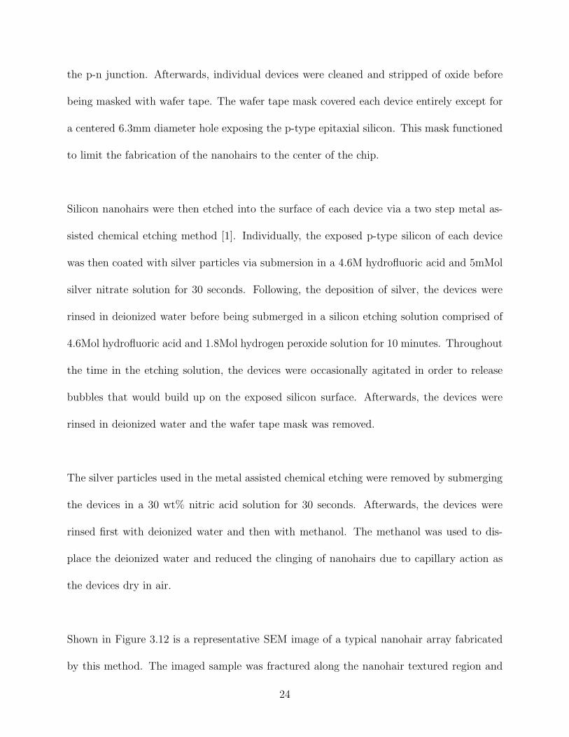
Shown in Figure 3.12 is a representative SEM image of a typical nanohair array fabricated
by this method. The imaged sample was fractured along the nanohair textured region and
24

the cross-section imaged at 45 degrees. The silicon nanohairs appear as vertical lighter gray
structures several microns in length. In the upper half of the image, the nanohairs are found
to have spaces between them that will be back filled in the following process step. Full
characterization of the nanohair height and distribution are reported in Chapter 4.
Figure 3.12: 45 degree SEM cross-section of typical nanohair array fabricated via the MACE process
25

3.2 Nanohair Backfill/Passivation
3.2.1 Process
Device fabrication proceeds with the back-filling of the spaces between the silicon nanohairs.
Figure 3.13 shows the schematic of the nanohair textured device following this process. The
entire device was coated with aluminum oxide via atomic layer deposition. This not only
had the effect of backfilling the spaces between nanohairs, but also coated the n+ cap, on
the side opposite the nanohairs. This potentially reduced shorting around the exposed p-n
junction on the sides of the device.
26

Figure 3.13: Top view (a) and cross-section view (b) of the nanohair textured device following the backfillof the silicon nanohair textured surface
Samples were batch coated with aluminum oxide via atomic layer deposition using an Ox-
ford Instruments OpAl. The OpAl was first prepared for the deposition by pre-heating the
stage to 200C. Following, the devices were placed on the OpAl stage such that the nanohair
textured surface was facing upwards. A total thickness of 0.14um of aluminum oxide was
then deposited over 1500 cycles of the atomic layer deposition process over approximately
2.5 hours.
27

3.2.2 Process Development
The p-n junction nanohairs posed a few challenges to device construction, particularly
in making ohmic contacts. Since the p-n junctions were exposed along the length of the
nanohairs, any contact between adjacent hairs was likely to cause shorting either between
the hairs or across the p-n junction. Additionally, the deposition of a top electrode risked
having the electrode material being deposited in the space between the nanohairs, which
could result in shorting of the p-n junction. The final issue was that the nanohairs could be
easily damaged by even the slightest mechanical contact to their surface. For these reasons,
we investigated several means for the deposition of a dielectric material between the p-n
junction silicon nanohairs.
Candidate deposition methods for the dielectric backfill had to be able to deposit material
in the spaces between the nanohairs. This posed a challenge considering the distance be-
tween nanohairs was on the order of 100nm; limiting the ability of the deposited material
to reach the base of the nanohairs. Additionally, it had to be possible to selectively remove
the candidate material from the silicon surface. Selective remove of the candidate material
was essential to exposing the nanohair tips in order to later make electrical contact to the
silicon surface.
28

The candidate materials and their associated methods of deposition were as follows;
• Silicon Dioxide, Plasma Enhanced Chemical Vapor Deposition: Excellent
insulator, excellent etch selectivity over silicon, fairly conformal deposition
• 20 nm (average) Titanium Dioxide nanoparticles, Nanoparticle Solution De-
position: Good insulator, good etch selectivity over silicon, nanoparticles are smaller
than space between nanohairs
• JR White Epoxy, Solvent Casting: Good insulator, excess material can be me-
chanically polished to expose silicon nanohair tips, fairly conformal deposition
• Parylene, Vapor Deposition: Good insulator, fairly conformal deposition
• Aluminum Oxide, Atomic Layer Deposition: Good insulator, good etch selec-
tivity over silicon, very conformal deposition
Each of these methods were tested with 1cm by 1cm silicon nanohair samples made with
p-type silicon wafers. The silicon nanohair samples were fabricated via the metal assisted
wet chemical etching process described in the preceding section. After being subjected to the
backfill deposition method, the samples were fractured and the cross-sections were imaged by
scanning electron microscope to determine if the material was successfully deposited between
the nanohairs. Shown in Figures 3.14 through 3.18 are representative 45 degree scanning
electron microscope cross-sections for each method.
29
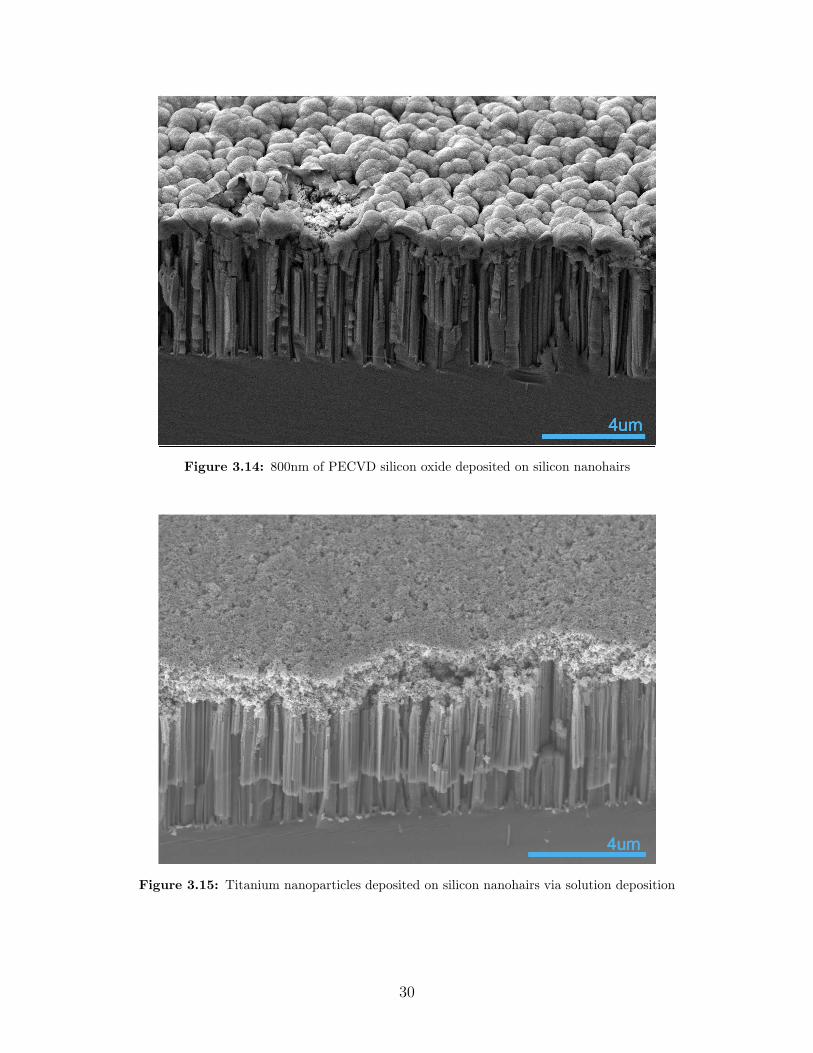
Figure 3.14: 800nm of PECVD silicon oxide deposited on silicon nanohairs
Figure 3.15: Titanium nanoparticles deposited on silicon nanohairs via solution deposition
30

Figure 3.16: JR White epoxy deposited on silicon nanohairs via solvent casting
Figure 3.17: Parylene deposited on silicon nanohairs via vapor deposition
31

Figure 3.18: Atomic layer deposition aluminum oxide deposited on silicon nanohairs
The plasma enhanced chemical vapor deposition of silicon dioxide was found to be unsuc-
cessful in backfilling the spaces between the silicon nanohairs. Silicon dioxide was found
to build up on the tips of the nanohairs, eventually blocking access to the spaces between
nanohairs. The result of this effect is seen in Figure 3.14 as a light gray colored layer of
silicon oxide resting above the array of nanohairs.
The solution deposition of titanium nanoparticles was found to be unsuccessful in backfilling
the spaces between silicon nanohairs. From the SEM images in Figure 3.15, it was deter-
mined that the silicon nanoarticles primarily deposited above the silicon nanohairs with few
filling the spaces between nanohairs. This could be the result of the nanoparticles conglom-
erating into particles too large to penetrate the spaces between nanohairs. Alternatively,
the solution in which the particles were suspended may have been unable to penetrate the
32

spaces between nanohairs due to surface tension.
The solvent casting of JR White epoxy was found to be successful in backfilling the spaces
between nanohairs. This is shown in Figure 3.16 as a smooth gray material in between the
lighter gray vertical nanohair structures. However, there is a visible large amount of excess
JR White expoxy above the silicon nanohairs that may pose a challenge for removal.
The vapor deposition of parylene was found to be unsuccessful in backfilling the spaces be-
tween nanohairs. As with the plasma enhanced chemical vapor deposition of silicon oxide,
parylene was found to build up on the tips of the nanohairs, eventually preventing access to
the spaces between the nanohairs. In Figure 3.17, parylene is shown as a dark gray material
resting on top of a lighter gray vertical array of nanohairs. Little or no parylene can be
found between the nanohairs.
The atomic layer deposition of aluminum oxide was found to be successful in backfilling the
spaces between nanohairs. Figure 3.18 shows the aluminum oxide as a dark gray in between
the lighter gray of the silicon nanohairs. Few to no gaps are found between the nanohairs,
suggesting that the aluminum oxide deposition is very conformal.
From these results, the atomic layer deposition of aluminum oxide was chosen as the method
to be used for the nanohair backfill. Of the tested methods, only the solvent casting of JR
White epoxy and the atomic layer deposition of aluminum oxide were found to be able to
penetrate the spaces between the nanohairs. However, Aluminum oxide was chosen in favor
33
of JR White due to the ability to etch aluminum oxide selectively over silicon.
3.2.3 Surface Passivation via Thermal Oxidation
Passivation of the silicon nanohair surface using thermally grown silicon oxide was also inves-
tigated. This method of passivation was thought to be promising because thermally grown
silicon oxide is conformal to the silicon surface surface. Therefore, it should readily coat
all of the nanohair surface. Additionally, silicon oxide is a great passivating material, with
only a thin layer of material (≈ 10nm) necessary to passivate the silicon surface. However, it
was uncertain whether or not the silicon nanohairs would be damaged by the thermal process.
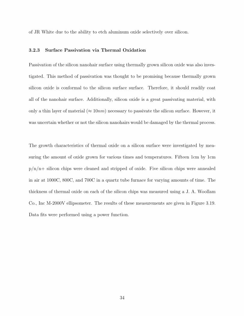
The growth characteristics of thermal oxide on a silicon surface were investigated by mea-
suring the amount of oxide grown for various times and temperatures. Fifteen 1cm by 1cm
p/n/n+ silicon chips were cleaned and stripped of oxide. Five silicon chips were annealed
in air at 1000C, 800C, and 700C in a quartz tube furnace for varying amounts of time. The
thickness of thermal oxide on each of the silicon chips was measured using a J. A. Woollam
Co., Inc M-2000V ellipsometer. The results of these measurements are given in Figure 3.19.
Data fits were performed using a power function.
34

0 25 50 75 100 125 150
Time (min)
0
50
100
150
200
Thic
kness (
nm
)
Thermal Oxidation Curves of p-type Silicon for Various Temperatures
1000C Data
1000C Fit
800C Data
800C Fit
700C Data
700C Fit
Figure 3.19: Measured and fitted thermal oxidation characteristics of p-type epitaxial silicon
From these oxidation curves, it was determined that oxidation at 800C for 15 minutes would
yield the desired ≈ 10nm of silicon oxide for surface passivation. This thickness of silicon
oxide was chosen because it is around the minimum amount required to passivate the surface.
Further oxidation of the nanohairs risks consuming a significant amount of the nanohair sil-
icon, given that the diameter of the nanohairs is ≈ 50nm.
Silicon nanohair samples were prepared on 1cm by 1cm p/n/n+ silicon chips using the pro-
cess described in the previous section. These samples were annealed in air in a tube furnace
at 800C for 15min. The samples were then fractured down the center of the chips and the
cross-sections were imaged using a scanning electron microscope. Shown in Figure 3.20 is a
representative image of the oxidize nanohairs.
35

Figure 3.20: 45 degree SEM cross-section of silicon nanohairs thermally oxidized in air at 800C for 15min
The silicon nanohairs were found to be largely undamaged by the annealing process. This is
evidenced by their structure appearing similar to before the anneal (Figure 3.12). However,
the thickness of thermal oxide could not be determined. Although the oxidation curves
suggest that the silicon oxide thickness should be about 10nm, nanohair textured surfaces
could oxidize at a higher rate than the planar surfaces used to produce the oxidation curves.
This could be investigated experimentally by imaging individual oxidized nanohairs with
a transmission electron microscope. However, this experiment was not attempted in this
research.
36

3.3 Nanohair Tip Exposure
3.3.1 Process
Device fabrication proceeded with the removal of excess aluminum oxide resulting from the
nanohair backfill process. Figure 3.21 shows the schematic of the nanohair textured device
following this process. Aluminum oxide was selectively removed from the nanohair textured
surface such that the tips of the nanohairs are exposed. This excess aluminum oxide must
be removed in order to make electrical contact to the p-type silicon nanohair surface. The
aluminum oxide layer was preserved on the p-type field silicon as well as the sides and back
of the device. This was done in order to protect the n+ silicon cap as well as potentially
reduce shorting around the exposed p-n junction on the side of the silicon chip.
37

Figure 3.21: Top view (a) and cross-section view (b) of the nanohair textured device following the exposureof the nanohair tips
Devices were masked with wafer tape such that only the nanohair textured area was exposed.
Afterwards, the devices were submerged in a 5 wt% hydrofluoric acid solution for 90 seconds.
Devices were placed in solution such that the exposed surface was upward facing. This
solution etched away the excess aluminum oxide from the nanohair tips, but did not remove
the aluminum oxide from between the nanohairs. Following the time in solution, the devices
were thoroughly rinsed in deionized water and dried with nitrogen. The wafer tape was left
38

on the devices for the next process step.
3.3.2 Process Development
After backfilling the spaces between the silicon nanohairs via atomic layer deposition of alu-
minum oxide, the tips of the nanohairs lie beneath a surface of aluminum oxide. In order
to make electrical contact to the nanohair tips this surface of aluminum oxide must be re-
moved. To accomplish this, we investigated the use of selective wet chemical etching in order
to remove excess aluminum oxide from the nanohair tips.
According to Thin film processes, by Vossen & Kern, table of chemical etchants for thin
films, the recommended wet etches for Al2O3 are hydrofluoric acid or hot phosphoric acid.
[2] For this process, hydroflouric acid was chosen in favor of hot phosphoric acid. This was
done in order to eliminate the added complexity of maintaining a consistent solution tem-
perature. Additionally, HF is desirable because of its reported high etch rate that could be
controlled through simple dilution as well as it’s high selectivity over silicon.
Experimental determination of the etch rate of atomic layer deposition aluminum oxide be-
gan by depositing 100nm of aluminum oxide on five 1cm by 1cm silicon chips. Each of
these chips were then submerged in a 5% hydrofluoric acid solution for a varying amount of
time between zero and 2 minutes. The silicon chips were placed in solution such that the
aluminum oxide coated surface was face up. Upon removal from the solution the chips were
thoroughly rinsed with deionized water and dried.
39
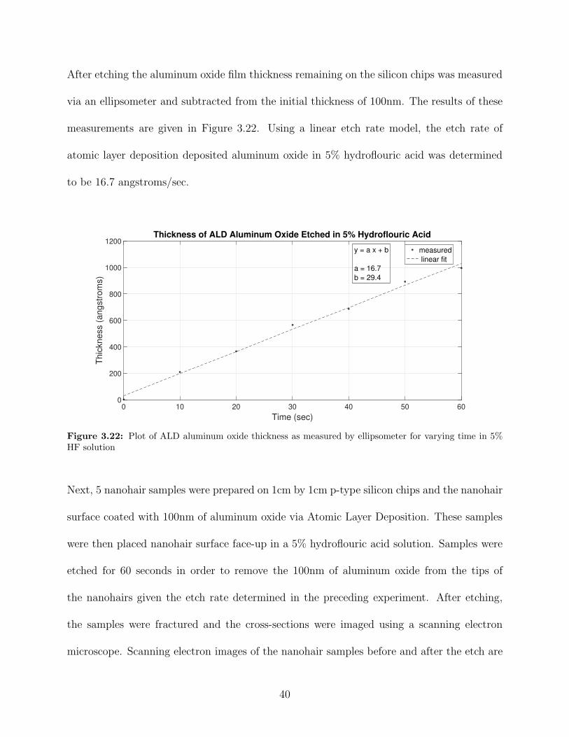
After etching the aluminum oxide film thickness remaining on the silicon chips was measured
via an ellipsometer and subtracted from the initial thickness of 100nm. The results of these
measurements are given in Figure 3.22. Using a linear etch rate model, the etch rate of
atomic layer deposition deposited aluminum oxide in 5% hydroflouric acid was determined
to be 16.7 angstroms/sec.
Time (sec)
0 10 20 30 40 50 60
Th
ickn
ess (
an
gstr
om
s)
0
200
400
600
800
1000
1200Thickness of ALD Aluminum Oxide Etched in 5% Hydroflouric Acid
measured
linear fit
y = a x + b
a = 16.7
b = 29.4
Figure 3.22: Plot of ALD aluminum oxide thickness as measured by ellipsometer for varying time in 5%HF solution
Next, 5 nanohair samples were prepared on 1cm by 1cm p-type silicon chips and the nanohair
surface coated with 100nm of aluminum oxide via Atomic Layer Deposition. These samples
were then placed nanohair surface face-up in a 5% hydroflouric acid solution. Samples were
etched for 60 seconds in order to remove the 100nm of aluminum oxide from the tips of
the nanohairs given the etch rate determined in the preceding experiment. After etching,
the samples were fractured and the cross-sections were imaged using a scanning electron
microscope. Scanning electron images of the nanohair samples before and after the etch are
40

shown in Figure 3.23 and Figure 3.24, respectively.
Figure 3.23: 45 degree SEM cross-section of aluminum oxide back-filled nanohairs before hydroflouric acidsolution back-etch
41

Figure 3.24: 45 degree SEM cross-section of aluminum oxide back-filled nanohairs after hydroflouric acidsolution back-etch
From the preceding SEM images, it was concluded that the wet chemical etching method
was successful in selectively etching the aluminum oxide over the silicon nanohairs. This
is evident in the images as surface of the samples can be seen to transition from relatively
smooth to rough. The surface roughness appears as the aluminum oxide surface etches away,
leaving only the now protruding silicon nanohair tips. This selectivity is also evident in the
cross-section, as gaps between the nanohairs can be seen to form following the wet chemical
etch.
It can also be seen that the wet chemical etch successfully removed excess aluminum oxide
42

while preserving aluminum oxide in between the silicon nanohairs. This is shown in the
contrast between materials in the SEM images. The aluminum oxide is evidenced by a darker
gray in between the lighter silicon nanohairs. Additionally, aluminum oxide is evidenced by a
rougher horizontal texturing, whereas the silicon nanohairs have a finer texture. Examination
of both images shows that aluminum oxide is present before and after the wet chemical etch
at a depth below the surface.
43
3.4 Planar Device: Surface Etch-back
3.4.1 Process
The p-type surface of the planar devices was etched back in order to match the amount
of silicon lost above the nanohair tips, tlost, during the nanohair fabrication process. This
was accomplished via the wet chemical etching of the n-type silicon surface. Shown in Fig-
ure 3.25 is a schematic of the planar device following this process step. Characterization of
the amount of silicon lost above the nanohair tips is reported in Chapter 4, Section 1.
44
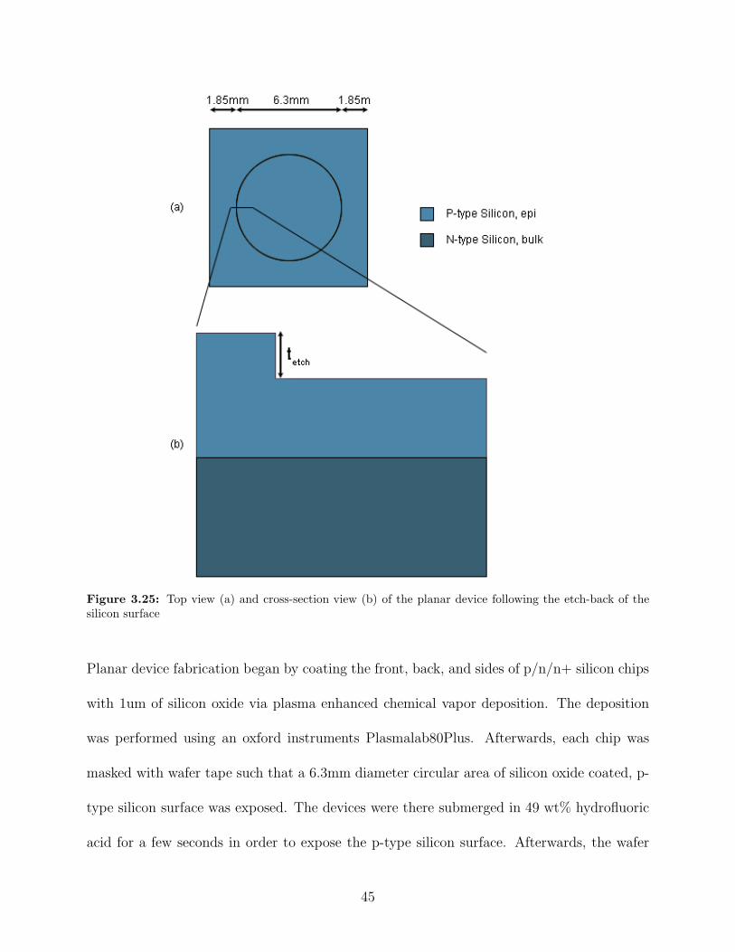
Figure 3.25: Top view (a) and cross-section view (b) of the planar device following the etch-back of thesilicon surface
Planar device fabrication began by coating the front, back, and sides of p/n/n+ silicon chips
with 1um of silicon oxide via plasma enhanced chemical vapor deposition. The deposition
was performed using an oxford instruments Plasmalab80Plus. Afterwards, each chip was
masked with wafer tape such that a 6.3mm diameter circular area of silicon oxide coated, p-
type silicon surface was exposed. The devices were there submerged in 49 wt% hydrofluoric
acid for a few seconds in order to expose the p-type silicon surface. Afterwards, the wafer
45

tape mask was removed. This completed the silicon oxide mask that would be used to limit
the surface etch to the centered circular area of the device.
The exposed p-type silicon surface was then etched by submerging the devices in a 45% potas-
sium hydroxide solution heated to 60C, for 6 minutes 36 seconds. The potassium hydroxide
solution was heated via a hot plate and the temperature of the solution was monitored using
an alcohol thermometer. Time in solution was measured via a stop watch. Upon removal
from the solution, the chips were thoroughly rinsed with deionized water, stripped of the
silicon oxide mask using hydrofluoric acid, and rinsed again.
3.4.2 Process Development
In the process of etching nanohairs into the silicon surface of the device, a small amount of
the silicon that is not in contact with Ag is also etched, reducing the thickness of the silicon
above the p-n junction. It is important to match this loss of silicon above the p-n junction
in the compared planar device since the junction lies only a few microns below the surface,
and the surface to junction distance has a very significant impact on light response (See
section 2, Chapter 2). In this section a controllable method to etch away a small quantity
of the silicon surface via wet chemical etching was developed. This is done by character-
izing the etch rate and testing the method’s ability to reproducibly etch to the desired depth.
The silicon etching solutions investigated for this process step were a hydrofluoric acid, nitric
acid, and acetic acid solution (HNA) as well as a potassium hydroxide solution. Attempts
46

to back-etch with an HNA solution were largely unsuccessful due to its rapid etch rate of
silicon. Attempts to slow the etch rate of the HNA solution by changing the relative concen-
trations of its consituents resulted in inconsistent etch rates between devices. However, the
potassium hydroxide solution yielded a considerably slower and more consistent etch rate.
As such, potassium hydroxide solution was chosen in favor of HNA for the back-etch process.
The etch rate of silicon in potassium hydroxide was experimentally determined via the fol-
lowing experiment. Seven 1cm by 1cm p/n/n+ [100] silicon chips were coated entirely with
1um of silicon oxide via plasma enhanced chemical vapor deposition. The deposition was
performed using an oxford instruments Plasmalab80Plus. Afterwards, each chip was masked
with wafer tape such that a 6.3mm diameter circular area of silicon oxide coated, p-type
silicon surface was exposed. The devices were there submerged in 49 wt% hydrofluoric acid
for a few seconds in order to expose the p-type silicon surface. Afterwards, the wafer tape
mask was removed. This completed the silicon oxide mask that would be used to limit the
surface etch to the centered circular area of the device.
The devices were then etched with a 45% potassium hydroxide solution heated to 60C, for
times ranging from 2-7 minutes. The potassium hydroxide solution was heated via a hot
plate and the temperature of the solution was monitored using an alcohol thermometer.
Time in solution was measured via a stop watch. Upon removal from the solution, the chips
were thoroughly rinsed with deionized water.
The etch depth of the silicon was measured via optical profilometer. The profilometer was
47
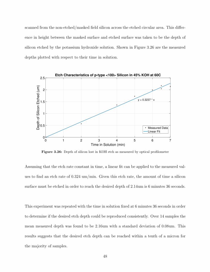
scanned from the non-etched/masked field silicon across the etched circular area. This differ-
ence in height between the masked surface and etched surface was taken to be the depth of
silicon etched by the potassium hydroxide solution. Shown in Figure 3.26 are the measured
depths plotted with respect to their time in solution.
Time in Solution (min)
0 1 2 3 4 5 6 7
De
pth
of
Sili
co
n E
tch
ed
(u
m)
0
0.5
1
1.5
2
2.5Etch Characteristics of p-type <100> Silicon in 45% KOH at 60C
Measured Data
Linear Fit
y = 0.3237 * x
Figure 3.26: Depth of silicon lost in KOH etch as measured by optical profilometer
Assuming that the etch rate constant in time, a linear fit can be applied to the measured val-
ues to find an etch rate of 0.324 um/min. Given this etch rate, the amount of time a silicon
surface must be etched in order to reach the desired depth of 2.14um is 6 minutes 36 seconds.
This experiment was repeated with the time in solution fixed at 6 minutes 36 seconds in order
to determine if the desired etch depth could be reproduced consistently. Over 14 samples the
mean measured depth was found to be 2.16um with a standard deviation of 0.08um. This
results suggests that the desired etch depth can be reached within a tenth of a micron for
the majority of samples.
48
3.5 Electrical Contacts
3.5.1 Process
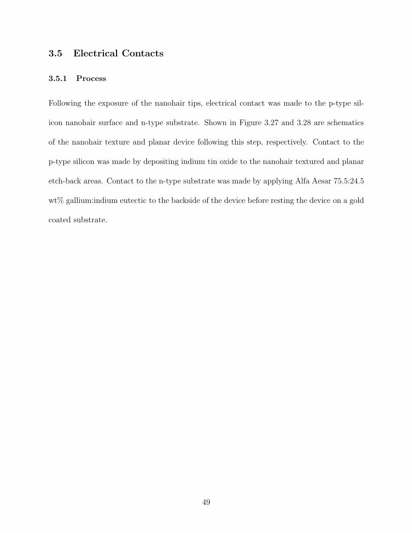
Following the exposure of the nanohair tips, electrical contact was made to the p-type sil-
icon nanohair surface and n-type substrate. Shown in Figure 3.27 and 3.28 are schematics
of the nanohair texture and planar device following this step, respectively. Contact to the
p-type silicon was made by depositing indium tin oxide to the nanohair textured and planar
etch-back areas. Contact to the n-type substrate was made by applying Alfa Aesar 75.5:24.5
wt% gallium:indium eutectic to the backside of the device before resting the device on a gold
coated substrate.
49

Figure 3.27: Top view (a) and cross-section view (b) of the nanohair textured device following the attach-ment of electrical contacts
50

Figure 3.28: Top view (a) and cross-section view (b) of the planar device following the attachment ofelectrical contacts
Following the exposure of the nanohair tips, the nanohair textured devices were still masked
with wafer tape such that only the nanohair textured area was exposed. Planar devices were
prepared similarly, by masking all but the p-type silicon area that was back-etched. The
devices were rinsed in 5% hydroflouric acid for 10 seconds in order to remove any native ox-
ide. Afterwards the exposed areas were coated with 1um of indium tin oxide via magnetron
51

sputtering. The deposition system used for this process was a AJA International Inc. ATC
2000-V with a Kurt J. Lesker In2O3/SnO2 90/10 wt% target. Nanohair textured devices
were coated using an DC applied bias and planar devices were coated using a AC applied
bias. This was done out of necessity, as the AC bias method first used on the planar devices
became inoperable, so all following nanohair devices used a DC bias method. Possible dif-
ferences in film characteristics are examined in Chapter 4.
Following the ITO deposition the wafer tape mask was removed and the devices were an-
nealed under nitrogen atmosphere for 30 minutes at 300C. This was done in order to increase
the transparency and conductivity of the indium tin oxide film. [3]
Following deposition of the top contact, electrical contact was made to the n+ cap of the
n-type substrate. However, at this point in the fabrication, aluminum oxide still covers the n-
type cap and must be removed prior to making electrical contact. In order to accomplish this,
the n-type side of the device was first masked with wafer tape such that a 0.63mm diameter
centered circular area is exposed. Following, a drop of 10% HF is left on the exposed surface
for 2min before the device was thoroughly rinsed and dried. This HF solution selectively
etched away the aluminum oxide without etching the n+ cap. The mask was removed and
the liquid gallium indium eutectic is then applied to the exposed silicon n+ cap. Afterwards,
the device was placed gallium indium eutectic side down on a gold coated kovar substrate,
completing the bottom contact.
52

3.5.2 Process Development
Considerations for electrical contact to the devices included silicon wafer dopant concen-
trations and contact materials. Silicon wafer dopant concentrations had to be considered
because successful ohmic contact is dependent upon both the contact material work function
as well as the Fermi level of the silicon. Additionally, electric contact to the nanohair tex-
tured surface was required to be transparent in order to allow light to reach the p-n junction.
Whereas, the electric contact to the silicon substrate was limited only by it’s integration into
the fabrication process.
Determination of electric contact to a given device was accomplished via measurement of
the current-voltage characteristics of the device. Current-voltage profiles were measured us-
ing a probe station and a Keithley 4200-SCS Semiconductor Parametric Analyzer. Voltage
was applied to the devices from -1V to 1V and current was measured. For ohmic contact,
the current voltage characteristics were anticipated to resemble that of non-ideal diode as
described in Chapter 2, Section 6. Non-ohmic contact was anticipated to resemble a null
current, indicating no electrical contact, or that of a Schottky diode, indicating a potential
barrier between the chosen contact and the silicon surface.
Investigation of electric contacts began with a p/n wafer. The silicon wafer was cut into
1cm by 1cm chips via dicing saw. Dicing saw cuts started from the n-type substrate surface,
stopping short of reaching the p-n junction. The remaining thickness of silicon connecting
individual chips was fractured in order to achieve a clean cleave through the p-n junction.
53
Following, the devices were cleaned and stripped of oxide with hydrofluoric acid.
Initial attempts to make electrical contact to the device involved only the use of various
types of metal probes contacting the silicon surface. This option was investigated first, be-
cause it required little integration into the final fabrication process flow. The metal probes
investigated were aluminum, tungsten, copper, and gold. However, none of these materials
were successful in making ohmic contact to the silicon surface. All measured current-voltage
characteristics resembled that of a Schottky diode or no current flow. Whether the poor elec-
trical contact was due to the n-type contact, p-type contact, or both could not be determined.
Following, the silicon wafer used for device fabrication was changed to a p/n/n+ wafer sup-
plied by Texas Instruments in Portland, Maine. This wafer had the same p-type and n-type
silicon concentrations as before, but an n+ capping layer was added by implanting arsenic
into the back (n-type) side of the wafer. This became the silicon wafer used for all following
devices. The n+ cap was added in order to improve electrical contact to the n-type substrate
via a tunnel contact created between the heavily doped silicon and the chosen metal contact.
Devices used for contact testing were prepared in the same way as the previous p/n devices.
In order to determine if the n+ cap would improve electrical contact to the n-type substrate,
ohmic contact first had to be made to the p-type silicon. To accomplish this, the p-type
surface was coated with and thermally alloyed with aluminum. This method was chosen,
because it is a common method of achieving ohmic contact to p-type silicon. Once ohmic
contact to the p-type silicon was made, the effect of the n+ cap could be investigated inde-
54

pendently.
A film of 1.4um of aluminum was deposited on to the p-type silicon of the devices via elec-
tron beam evaporation. Devices were masked with wafer tape prior to the deposition such
that the aluminum deposited on a centered circular area on the silicon chips. Following the
deposition, the devices were annealed under nitrogen atmosphere for 30 min at 450C. This
anneal functioned to alloy the deposited aluminum with the silicon surface.
The current-voltage characteristics of these devices were measured with various metal con-
tacts to the n+ cap of the devices. The metal contacts included copper, aluminum, tungsten,
gold, and 75.5/24.5 wt% gallium/indium eutectic (liquid at room temperature). Of these
contacts the gallium/indium paste was found to exhibit the best ohmic contact to the n+
cap with the measured current-voltage characteristics resembling that of a non-ideal diode
with corresponding dopant concentrations. As such, the gallium/indium eutectic became
the method of contact to the n+ cap for all following devices.
After establishing a method of contact to the n-type substrate, contact to the p-type sili-
con using a transparent conductor was investigated. The primary candidate was indium tin
oxide due to it’s well studied high conductivity and transparency. Samples were prepared
by depositing 1um of indium tin oxide via magnetron sputtering on a centered circular area
of p-type silicon through a wafer tape mask. Following, the current-voltage characteristics
were measured before and after annealing the devices under nitrogen atmosphere for 30min
at 300C. During measurement, contact was made to the n-type substrate using gallium in-
55
dium eutectic.
Both the annealed and non-annealed indium tin oxide contact devices were found to exhibit
ohmic contact. However, the non-annealed samples were found to have inferior contact as
evidenced by larger series resistance. This is in agreement with research that suggests that
annealing indium tin oxide in a nitrogen atmosphere will increase the conductivity of the
film. [3] As such, indium tin oxide became the method of contact to the p-type silicon.
56
REFERENCES
1. Zachary R. Smith, Rosemary L. Smith, Scott D. Collins, ”Mechanism of Nanowire
Formation in Metal Assisted Chemical Etching”, Electrochimica Acta, 92, 139-147,
2013.
2. John L. Vossen, Werner Kern, Thin Film Processes, Academic Press, New York, New
York, 1978, pgs. 433-480.
3. R. X. Wang, C. D. Beling, et. al., ”Influence of gaseous annealing environment on
the properties of indium-tin-oxide thin films”, Journal of Applied Physics, 97 033504,
2005.
57

CHAPTER 4: DEVICE CHARACTERIZATION
METHODS & RESULTS
4.1 Material Characterization of Deposited Materials
Various properties of aluminum oxide and indium tin oxide were characterized as a part of
their consideration for a back-fill and top electrode material, respectively. This character-
ization is essential in order to determine the contributions of these materials to the final
device performance. The properties investigated include ultra-violet/visible transmission
via UV-visible transmission spectroscopy and material composition via X-ray and Ultravio-
let photoelectron spectroscopy
All material characterization was performed on thin films of aluminum oxide and indium tin
oxide deposited onto glass slides (Fisher Scientific Premium Microscope Slides, 3in by 1in,
borosilicate). The indium tin oxide film was 1um in thickness and deposited by means of
a magnetron sputtering process before undergoing a post-deposition anneal at 300C under
nitrogen atmosphere for 30min. The aluminum oxide film was 0.14um in thickness and was
deposited via atomic layer deposition. The thickness of the ITO film was measured using
a Filmetrics F40-UV thin-film analyzer and the thickness of the aluminum oxide film was
measured using a J. A. Woollam Co., Inc M-2000V Ellipsometer. Full details of the film
deposition methods are given in Appendix I and II.
58

4.1.1 Ultraviolet-Visible Transmission Spectroscopy
The UV-visible transmission measurements were performed using an Ocean Optics DH-2000-
BAL light source and an Ocean Optics USB400 spectrometer. The transmission spectrum
of a bare microscope slide was measured first to be used as a baseline reference before
measuring the thin film samples. All measurements were performed within a dark box in
order to limit the incident light to only the Ocean Optics light source. The transmission
spectra obtained for the aluminum oxide and indium tin oxide films are shown in Figure 4.29.
Figure 4.29: Transmission spectrum of magnetron sputtered indium tin oxide and atomic layer depositionaluminum oxide films
It can be seen that the aluminum oxide film is very transparent across all measured wave-
59

lengths. As such the aluminum oxide used to fill the voids between nanohairs should have
little effect on the light reaching the p-n junction. However, the Magnetron Sputtered ITO
absorbs more light than the aluminum oxide across almost all wavelengths, but especially
in the near UV. This is despite a significant increase in transparency following the post-
deposition anneal. Below a wavelength of 400nm, transmission decreases below 50% in
annealed ITO. This lower transmittance is likely to reduce the effectiveness of the final de-
vices in the UV range. No difference in transmission spectra was measured between the AC
and DC sputtered ITO used for planar and nanohair textured devices, respectively.
4.1.2 X-ray Photo-electron Spectroscopy
X-ray photo-electron spectroscopy measurements were performed using a 1481.61eV X-ray
source and a SPECS PHOIBOS HSA3000 MCD5 hemispherical energy analyzer. Photo-
electron emission was measured across a binding energy range of 0−1300eV . Data collection
and compositional analysis were performed using SpecsLab2, Version 2.55-r18120 software.
The observed spectra of the aluminum oxide and indium tin oxide films after annealing are
given in Figure 4.30 and 4.31.
60

100150200250300350400450500550600
Binding Energy (eV)
0
0.5
1
1.5
2C
ou
nts
(#
)10
4
X-ray Photoelectron Spectroscopy Spectra of Atomic Layer Deposition
Aluminum Oxide
O 1s
C 1s
Al 2s
Al KLL
Al 2p
Element Atomic Percent
Oxygen 47.85
Aluminum 52.15
Figure 4.30: Measured characteristic energy lines and material composition of atomic layer depositionaluminum oxide
420440460480500520540
Binding Energy (eV)
0
1
2
3
4
5
Co
un
ts (
#)
104
X-ray Photoelectron Spectroscopy Spectra of Magnetron Sputtered
Indium Tin Oxide
O 1s
Sn 3d3/2
Sn 3d1/2
In 3d3/2
In 3d1/2
Element Atomic Percent
Oxygen 56.64
Tin 3.79
Indium 41.57
Figure 4.31: Measured characteristic energy lines and material composition of annealed magnetron sput-tered indium tin oxide
The atomic layer deposition aluminum oxide film was found to be consistent with expecta-
tions. The composition of the aluminum oxide film was found to be non-stoichiometric with
61
a deficiency of oxygen and some carbon impurity. The carbon impurity is likely due to the
presence of hydrocarbons on the film surface rather than from the film itself. The reduced
oxygen fraction may be due to incomplete oxidation during deposition by the water vapor.
This could be the result of too short of a cycle time being used in the atomic layer deposition
process.
The magnetron sputtered indium tin oxide film was found to be indium rich after annealing
in comparison to the target material composition used in the deposition as well as reported
values of untreated ITO films. [1,2] The Kurt J. Lesker ITO target used for the deposi-
tion has a reported atomic percent composition of 30% indium, 10% tin, and 60% oxygen.
Additionally, the ITO deposition was performed with an oxygen atmosphere, so a larger
concentration of oxygen was to be expected. It is possible that the bulk composition of the
ITO film more closely aligns with the expected composition, but there exists a larger con-
centration of metallic indium at the film surface. It has been reported that an indium rich
film may form at the ITO surface due to the migration of oxygen from In2O3−x phases when
annealed in the absence of oxygen. [2,3] This migration results in an increased concentration
of metallic indium at the surface as the oxygen migrates to form more In2O3 phases. No
difference in XPS spectra was measured between the AC and DC sputtered ITO used for
planar and nanohair textured devices, respectively.
4.1.3 Ultraviolet Photo-electron Spectroscopy
Ultraviolet photo-electron spectroscopy measurements were performed using a 22.2eV helium
plasma ultraviolet light source and a SPECS PHOIBOS HSA3000 MCD5 hemispherical en-
62
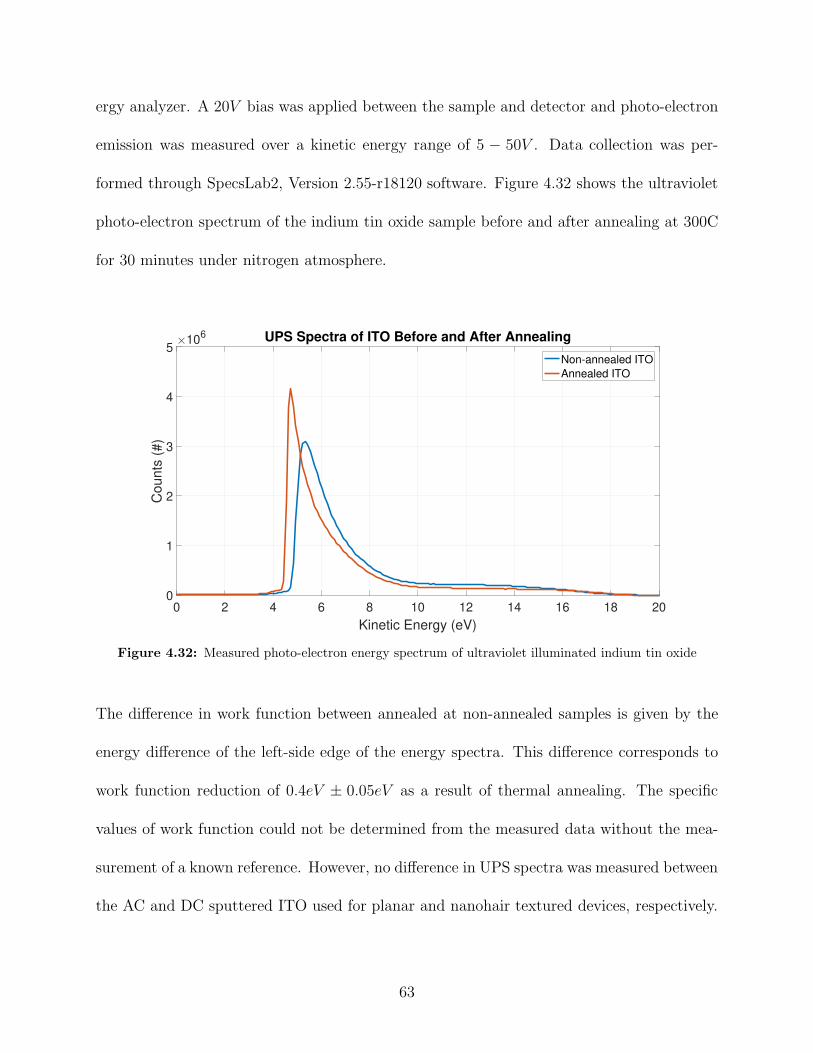
ergy analyzer. A 20V bias was applied between the sample and detector and photo-electron
emission was measured over a kinetic energy range of 5 − 50V . Data collection was per-
formed through SpecsLab2, Version 2.55-r18120 software. Figure 4.32 shows the ultraviolet
photo-electron spectrum of the indium tin oxide sample before and after annealing at 300C
for 30 minutes under nitrogen atmosphere.
0 2 4 6 8 10 12 14 16 18 20
Kinetic Energy (eV)
0
1
2
3
4
5
Counts
(#)
106 UPS Spectra of ITO Before and After Annealing
Non-annealed ITO
Annealed ITO
Figure 4.32: Measured photo-electron energy spectrum of ultraviolet illuminated indium tin oxide
The difference in work function between annealed at non-annealed samples is given by the
energy difference of the left-side edge of the energy spectra. This difference corresponds to
work function reduction of 0.4eV ± 0.05eV as a result of thermal annealing. The specific
values of work function could not be determined from the measured data without the mea-
surement of a known reference. However, no difference in UPS spectra was measured between
the AC and DC sputtered ITO used for planar and nanohair textured devices, respectively.
63

The reduction of ITO work function as a result of thermal annealing under nitrogen atmo-
sphere is in agreement with recent research. [1,2] This reduction in work function is thought
to be the result of the reduction of oxygen at the film surface. This increases the relative
amount of metallic indium, reducing the work function to be more near the 4.09eV of metal-
lic indium. This theory is also agreement with the results of the XPS experiment, detailed
in the previous section, indicating the presence of an indium rich surface of the ITO film.
4.1.4 4-Point Conductivity
Conductivity of the indium oxide film was measured before and after annealing during the
process step described in Chapter 3, Section 5 using a 4-point probe measurement system.
The 4-point probe tip used had a tungsten carbide probe tip from Signatone with a tip spac-
ing of 40mils. A current of 1mA was applied to the probe using a Keithley 2400 SourceMeter
and voltage was measured by the same device.
The measured voltage of the pre-anneal and post-anneal devices were found to be 8.0mV
and 2.4mV respectively. The sheet resistance, ρsheet, of the films was then calculated using
the following equation:
ρsheet =π
ln(2)
V
I(4.8)
The pre-anneal and post-anneal indium tin oxide films were found to have a sheet resistance
of 36ohms/sq and 11ohm/sq, respectively.
64

4.2 Device Morphology
4.2.1 p-n Junction Area Loss in Silicon Nanohair Fabrication
Fabrication of silicon nanohairs though a p-n junction requires that some of the original p-n
junction area is lost to the etching process. If the silicon nanohair textured device is to be
compared to a planar device of similar junction area, the fraction of area lost during the
silicon nanohair fabrication process must be taken into account. The following experiment
attempts to quantify the p-n junction area loss through the analysis of scanning electron
microscope images of silicon nanohair textured surfaces.
Silicon nanohair samples were prepared via metal enhanced wet chemical etching of p/n/n+
silicon wafer cut into 1cm by 1cm chips. The nanohair textured surfaces were then imaged
by scanning electron microscopy at a magnification of 5000X. Multiple images of the surface
were taken for each sample with six samples imaged in total. Shown in Figure 4.33 is a repre-
sentative image of the nanohair textured surfaces. Voids between the nanohairs are shown in
the SEM image as dark regions where as the tips of the nanohairs are shown as lighter regions.
65

Figure 4.33: Representative SEM top-view image of a silicon nanohair textured surface
All SEM images were converted into numerical matrices containing their grayscale pixel val-
ues. Pixel values ranges were normalized such that they ranged from 0-255 where 0 and 255
were white and black respectively and values in between are shades of gray. All grayscale
arrays were then subjected to a threshold function where the values below the threshold were
assigned a value of zero and those above the threshold were assigned a value of one. The
value of the threshold was chosen such that dark pixels of the nanohair voids fall below the
threshold and the lighter pixels indicating the tips of nanohairs lie above the threshold. The
mean value of the numerical arrays then yielded the ratio of area of silicon nanohair tips to
voids.
66

In order to determine the ideal threshold value, a range of values were used and the value
which best differentiated nanohair tips from voids was chosen. Shown in Figure 4.34 is a
representative scanning electron microscope image of the silicon nanohair surfaces with var-
ious thresholds applied. Overlaid on top of the original scanning electron microscope image
is a green shading indicating the areas marked as nanohair surfaces for the given threshold.
The ideal threshold was chosen as 50± 5 as this threshold visually appeared to best overlap
with the nanohair surfaces. For this threshold value, the nanohair tip surface area was found
to be 60% of the image surface with a standard deviation of 3% across fifty images. This
result suggests that 40±3% of the silicon p-n junction area is consumed in the metal assisted
chemical etching process.
67

Figure 4.34: Intensity map of imaged nanohair surface (shown in green) for various applied thresholdvalues
4.2.2 Characterization of Lost Nanohair Height
In the process of etching nanohairs into the silicon surface of the device, some of the silicon
which is not touching silver is also removed, albeit at a slower rate. This reduces the height
of the nanohair tips below the original silicon surface. The amount of silicon lost must be
characterized in order to determine the location of the p-n junction along the length of the
nanohairs. Knowing the location of the p-n junction is essential to characterizing the final
68
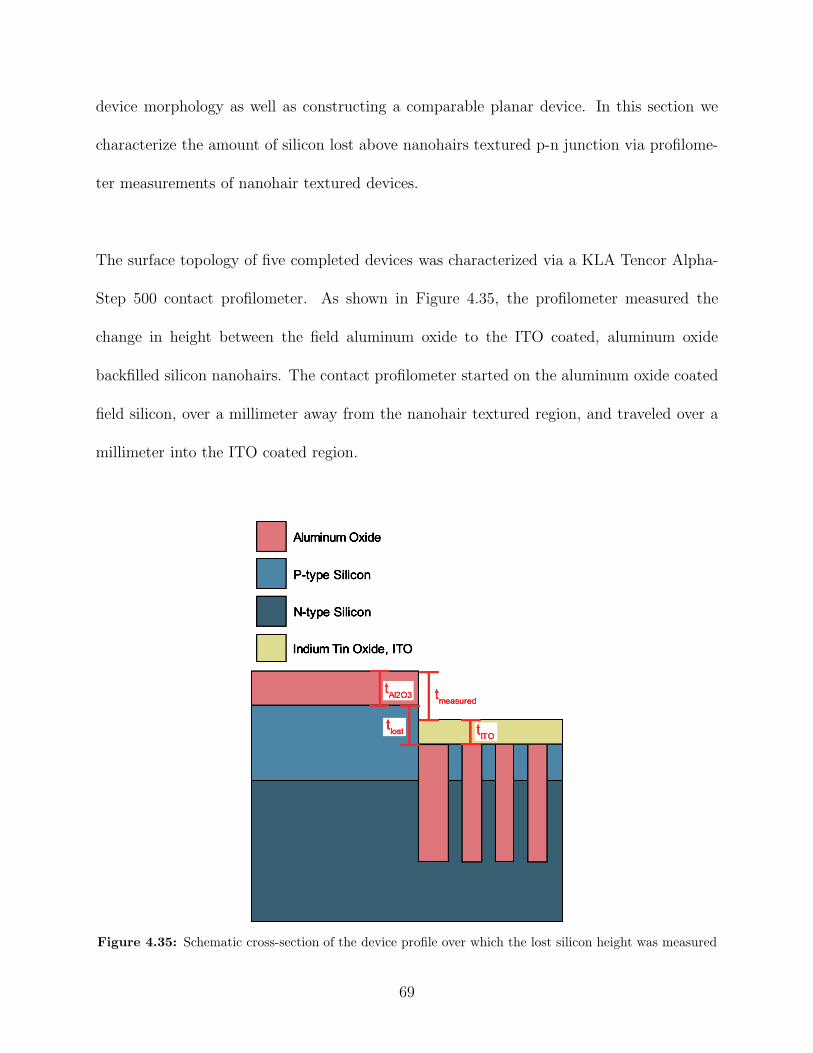
device morphology as well as constructing a comparable planar device. In this section we
characterize the amount of silicon lost above nanohairs textured p-n junction via profilome-
ter measurements of nanohair textured devices.
The surface topology of five completed devices was characterized via a KLA Tencor Alpha-
Step 500 contact profilometer. As shown in Figure 4.35, the profilometer measured the
change in height between the field aluminum oxide to the ITO coated, aluminum oxide
backfilled silicon nanohairs. The contact profilometer started on the aluminum oxide coated
field silicon, over a millimeter away from the nanohair textured region, and traveled over a
millimeter into the ITO coated region.
Figure 4.35: Schematic cross-section of the device profile over which the lost silicon height was measured
69
The measured change in height, tmeasured, was then used to calculate the height of silicon
lost to the nanohair etching process, tlost, via the following relationship;
tlost = tITO + tmeasured − tAl2O3 (4.9)
Where, tITO and tAl2O3 were the thicknesses of ITO and aluminum oxide deposited in the
bask-fill and transparent contact process steps. The thicknesses of these films were measured
to be 1.0um and 0.14um, respectively. Therefore, the amount of silicon lost in the nanohair
etching process was measured to have a mean of 2.14um with a standard deviation of 0.23um
across 14 devices.
4.2.3 Device Cross-sections
Device morphology was characterized by fracturing the completed nanohair textured devices
and imaging the cross-section of the device area. Images were collected using a scanning
electron microscope with the fractured edge angled at 45 degrees relative to the electron
beam. Representative nanohair devices were chosen for imaging based upon their overall
performance under illumination. These representative devices were selected at both the
higher and lower extremes of the performance distribution in order to determine what mor-
phological characteristics may contribute to the variability in device performance.
Shown in Figure 4.36 and Figure 4.37 are scanning electron microscope cross-sections of
nanohair textured devices representative of the upper and lower extremes of performance.
Seen in either image are the light colored vertical silicon nanohair structures with the darker
70

aluminum oxide filling the space between them. Above the nanohairs is a poly-crystalline
film of indium tin oxide.
Figure 4.36: 45 degree SEM cross-section of a nanohair textured device representative of the upper per-formance extreme
71

Figure 4.37: 45 degree SEM cross-section of a nanohair textured device representative of the lower perfor-mance extreme
The nanohair length was found to be consistent between upper and lower performance de-
vices. Across the measured devices the length was measured to be 4.1um with a standard
deviation of 0.3um. This consistency suggests that nanohair length may not be a significant
contributing factor to the observed variation in device performance. However, the overall
effect of nanohair length on device performance is unclear.
Upper performance devices were found to have more uniform nanohair distribution, more uni-
form dimensions, and more complete aluminum oxide back-filling than lower performance de-
vices. As seen in Figure 3.8, the higher performance devices display a more regular nanohair
72

structure with greater separation between the nanohairs. This allows for the atomic layer
deposition aluminum oxide to more effectively back-fill the space between the nanohairs.
This leaves few gaps between the nanohairs and likely contributes to greater surface state
passivation. In contrast, the lower performance devices display a lesser amount of nanohair
separation. This likely results in the observed larger number of gaps between the nanohairs
as the atomic layer deposition aluminum oxide is less able to penetrate the areas between
the nanohairs.
The location of the p-n junction depletion layer was determined to be fully along the length of
the nanohairs. This was determined from the measured nanohair length, the measured height
of silicon lost in the nanohair etch, the thickness of the epitaxial layer of p-type silicon, and
the calculated depletion layer thickness. With all of these values determined, the morphol-
ogy of the average nanohair textured device can be determined to be as shown in Figure 4.38.
Figure 4.38: Schematic cross-section of the measured nanohair texture device morphology
73

Variation in nanohair length and height of silicon lost in nanohair etch will result in more
or less of the depletion layer along the length of the nanohairs. This likely has an effect
on the performance of the devices, but there is insufficient information to make a confident
conclusion.
74

4.3 Photovoltaic Response Measurements
4.3.1 Experimental Setup
The current/voltage characteristics of the completed devices under various sources of illu-
mination were measured using the setup shown in Figure 4.39. A probe station was used
to make contact to the device while a semiconductor parametric analyzer applied a voltage
across the device and measured the current output. The voltage applied to the devices was
swept from -1V to +1V in order to investigate both forward and reverse bias characteristics.
Figure 4.39: Schematic of the setup used to measure the diode characteristics and photovoltaic responseof the nanohair textured and planar devices
The current/voltage characteristics of the devices were measured in the dark and exposed to
several sources of illumination. The light sources used to measure the photovoltaic response
of the devices were a Newport LCS-100 AM 1.5 solar emulator, a UVP UVL-21 ultra-violet
lamp, and a ThorLabs CPS405 405nm blue laser. The spectra of each source was measured
using an Ocean Optics USB400 spectrometer and are given below in Figure 4.40. All devices
75
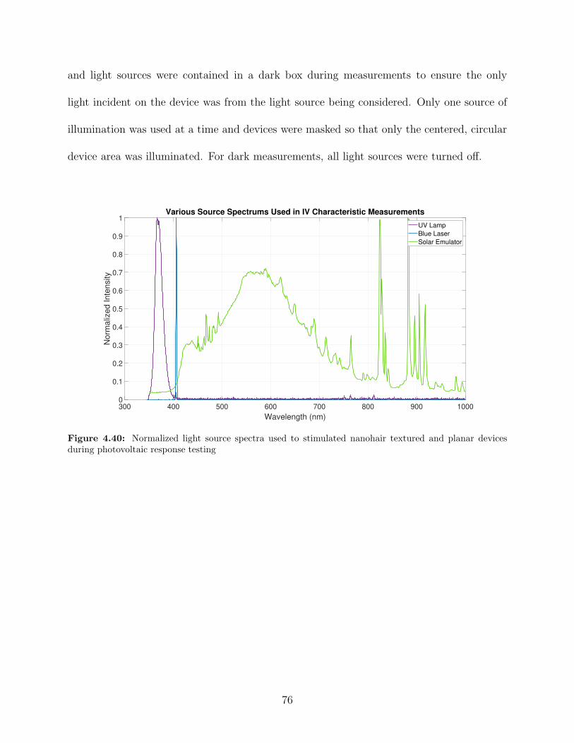
and light sources were contained in a dark box during measurements to ensure the only
light incident on the device was from the light source being considered. Only one source of
illumination was used at a time and devices were masked so that only the centered, circular
device area was illuminated. For dark measurements, all light sources were turned off.
300 400 500 600 700 800 900 1000
Wavelength (nm)
0
0.1
0.2
0.3
0.4
0.5
0.6
0.7
0.8
0.9
1
No
rma
lize
d I
nte
nsity
Various Source Spectrums Used in IV Characteristic Measurements
UV Lamp
Blue Laser
Solar Emulator
Figure 4.40: Normalized light source spectra used to stimulated nanohair textured and planar devicesduring photovoltaic response testing
76

4.3.2 Current/Voltage Characteristics: Dark
Figure 4.41 shows representative current/voltage curves for the typical nanohair textured
and planar devices. Diode properties of the planar and nanohair devices were found by
fitting the measured curves of 15 nanohair textured and 13 planar devices to the circuit
model described in the Section 2.6. Data fitting was performed using the linear regression
technique described in Chapter 2, Section 6. The mean values and standard deviation for
each fitted property are given in Table 4.1.
Figure 4.41: Non-illuminated current/voltage relationships for representative nanohair and planar devices
77

Nanohair (N=15) Planar (N=13)Property Mean σ Mean σ Difference (σ)Series Resistance, Rs (ohms) 237 88 139 90 0.55Shunt Resistance, Rsh (ohms) 11000 4000 240000 140000 1.6Saturation Current, Is (A) n/a n/a 3E-08 2E-08 n/aSaturation Ideality Factor, ns n/a n/a 1.59 0.15 n/aRecombination Current, Ir (A) 3E-06 2E-06 2E-07 3E-07 1.5Recombination Ideality Factor, nr 2.90 0.44 2.18 0.50 0.76
Table 4.1: Fitted circuit model values of 13 planar and 15 nanohair devices
Nanohair devices were found to have much more significant leakage as a result of their lower
shunt resistance. The difference in leakage is apparent in the magnitude of the current in the
reverse bias, where nanohair textured devices were found to produce orders of magnitude
more current. For an ideal diode the shunt resistance is very large, limiting the reverse bias
current to the saturation current of the diode until breakdown. However, both planar and
nanohair textured devices are non-ideal, having a secondary path for current around the
diode through the shunt resistance. The physical path being modeled by the shunt resis-
tance is likely caused by surface conduction around the p-n junction of the nanohairs. This
would stand to reason why nanohair textured devices are found to have much smaller shunt
resistances, resulting in a larger leakage current in the forward and reverse bias.
Nanohair devices were also shown to exhibit significantly greater recombination effects than
planar devices. This is evidenced by the difference in forward bias characteristics of the pla-
nar and nanohair textured devices. Planar devices are found to have a small recombination
region exhibited by a lower slope in the exponential behavior at the low forward bias and a
large active region exhibited by a larger slope in the exponential behavior for 0.2V − 0.4V
forward bias. Upon fitting these regions the saturation current, saturation ideality factor, re-
78

combination current, and recombination ideality factor can be found. However, the nanohair
devices are found to have a recombination region that dominates the forward bias right up
until series resistance effects begin to dominate around V = 0.4V . Upon comparing the
fitted recombination current values, the nanohair textured devices have much larger values,
indicating greater recombination effects. Additionally, the recombination ideality factor of
the nanohair textured devices was found to exceed the theoretical, upper limit of 2 for re-
combination inside the space charge region. This may suggest that the nanohair textured
devices have a secondary mechanism for recombination besides those found within the de-
pletion region of a planar device.
The increased recombination found in nanohair devices is likely a result of surface recombi-
nation effects. This is a form of electron-hole pair recombination due to electrons or holes
filling empty surface states of dangling bonds on the silicon surface. This effect is seen to
increase with respect to surface area and has been a known issue with nanoscale textured
microelectronic devices. [3,4,5] It can be reasoned that this is the primary reason for the
increased recombination since there are no other apparent differences between the nanohair
textured and planar devices that might result in differences in junction or bulk characteristics.
The series resistance values of nanohair and planar devices were found to be comparable.
Although the mean series resistance of nanohair devices was found to be larger, the difference
between the nanohair and planar devices is less than one standard deviation. This makes it
unclear whether the difference is physical or a result of variation in measurement. However,
it can be reasoned that the nanohair textured devices may have inferior electrical contact to
79

the ITO layer due to the surface roughness of the nanohair surface.
4.3.3 Current/Voltage Characteristics: Solar Simulator
Figure 4.42 shows the photovoltaic response of the average performing planar and nanohair
devices under 680Wm2 AM 1.5 solar simulated illumination. The plotted data is as measured
and does not account for the differences in junction area found in Section 1 of this chapter.
Table 4.2 gives the mean and standard deviation of values taken from all measured devices.
These values were fit from the photovoltaic response curves of each device using the defini-
tions described in Chapter 2, Section 7.
Figure 4.42: Current/voltage relationships for representative nanohair and planar devices under 680 W
m2
AM 1.5 solar simulated illumination
80
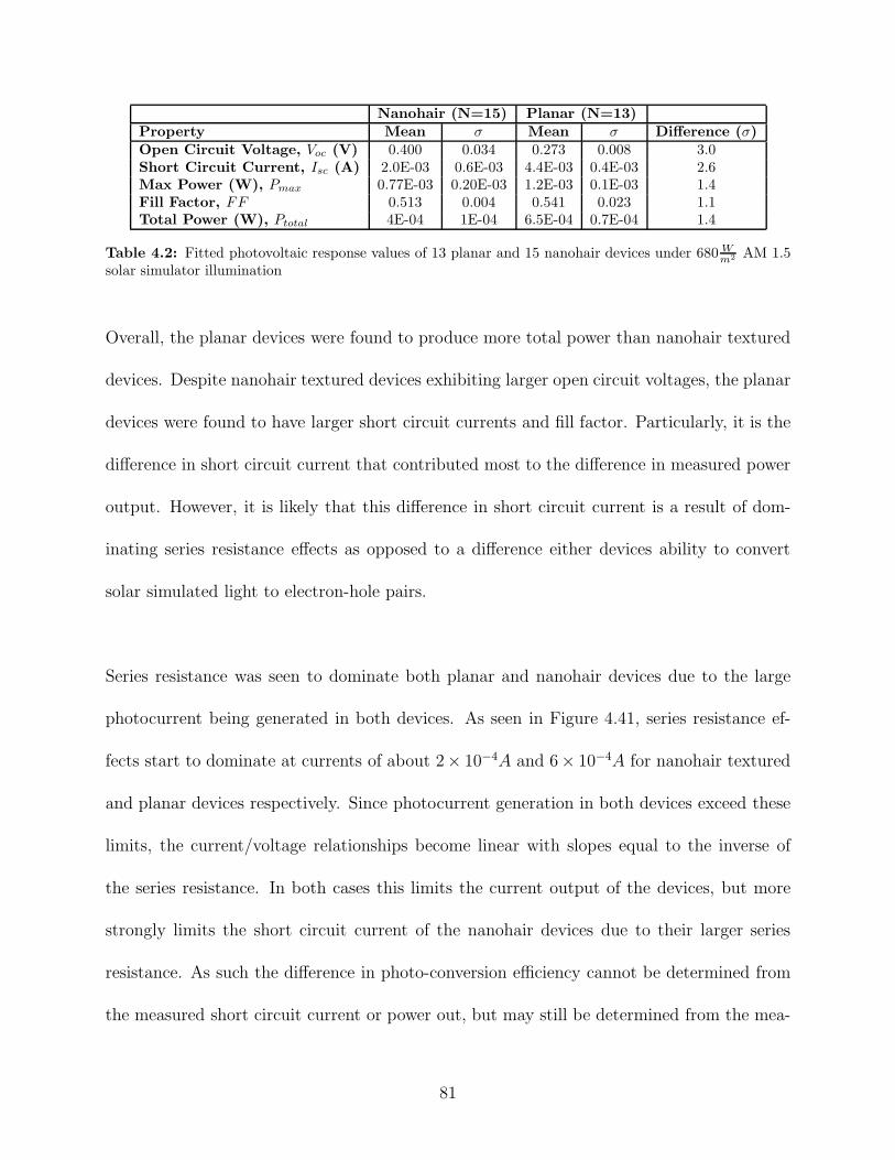
Nanohair (N=15) Planar (N=13)Property Mean σ Mean σ Difference (σ)Open Circuit Voltage, Voc (V) 0.400 0.034 0.273 0.008 3.0Short Circuit Current, Isc (A) 2.0E-03 0.6E-03 4.4E-03 0.4E-03 2.6Max Power (W), Pmax 0.77E-03 0.20E-03 1.2E-03 0.1E-03 1.4Fill Factor, FF 0.513 0.004 0.541 0.023 1.1Total Power (W), Ptotal 4E-04 1E-04 6.5E-04 0.7E-04 1.4
Table 4.2: Fitted photovoltaic response values of 13 planar and 15 nanohair devices under 680 W
m2 AM 1.5solar simulator illumination
Overall, the planar devices were found to produce more total power than nanohair textured
devices. Despite nanohair textured devices exhibiting larger open circuit voltages, the planar
devices were found to have larger short circuit currents and fill factor. Particularly, it is the
difference in short circuit current that contributed most to the difference in measured power
output. However, it is likely that this difference in short circuit current is a result of dom-
inating series resistance effects as opposed to a difference either devices ability to convert
solar simulated light to electron-hole pairs.
Series resistance was seen to dominate both planar and nanohair devices due to the large
photocurrent being generated in both devices. As seen in Figure 4.41, series resistance ef-
fects start to dominate at currents of about 2× 10⁻⁴A and 6× 10⁻⁴A for nanohair textured
and planar devices respectively. Since photocurrent generation in both devices exceed these
limits, the current/voltage relationships become linear with slopes equal to the inverse of
the series resistance. In both cases this limits the current output of the devices, but more
strongly limits the short circuit current of the nanohair devices due to their larger series
resistance. As such the difference in photo-conversion efficiency cannot be determined from
the measured short circuit current or power out, but may still be determined from the mea-
81

sured open circuit voltage values.
The difference in measured open circuit voltage values suggests that nanohair textured de-
vices more efficiently convert solar simulated light to electron-hole pairs than planar devices.
The open circuit voltage is the value of the potential created by the separation of photo-
generated electron-hole pairs across the p-n junction. As such, the larger open circuit voltage
found in nanohair textured devices suggest that more electron-hole pairs are being created
and/or separated by the built-in field in those devices than in planar devices. However, this
larger voltage does not in-turn result in a larger short circuit current due to the effects of
series resistance.
This experiment was repeated using the same devices with the intensity of the AM 1.5 solar
simulated illumination reduced to 13 Wm2 . By reducing the intensity of illumination on the
devices, the generated photo-current was reduced to a range under which series resistance
effects were less significant. The measured photovoltaic response of average representative
devices are shown in Figure 4.43. The mean and standard deviation of values fit from the
photovoltaic response curves of all devices are shown in Table 4.3. These values were fit from
the photovoltaic response curves of each device using the definitions described in Chapter 2,
Section 7. Full data distributions are given in Appendix VII.
82

Figure 4.43: Current/voltage relationships for representative nanohair and planar devices under 13 W
m2 AM1.5 solar simulated illumination
Nanohair (N=11) Planar (N=12)Property Mean σ Mean σ Difference (σ)Open Circuit Voltage, Voc (V) 0.29 0.03 0.278 0.008 0.28Short Circuit Current, Isc (A) 1.6E-04 0.1E-04 1.5E-04 0.1E-04 0.46Max Power, Pmax (W) 4.5E-05 0.4E-05 4.1E-05 0.2E-05 0.60Fill Factor, FF 0.71 0.04 0.85 0.01 2.8Total Power, Ptotal (W) 3.2E-05 0.4E-05 3.5E-05 0.2E-05 0.48
Table 4.3: Fitted photovoltaic response values of 12 planar and 11 nanohair devices under 13 W
m2 AM 1.5solar simulator illumination
Under these conditions the nanohair textured and planar devices were seen to be compa-
rable overall. Nanohair textured devices were found to have a similar or slightly larger
maximum power output, indicating a comparable or greater conversion of solar simulated
light to electron-hole pairs than planar devices. Series resistance effects no longer dominate
the current/voltage relationship of either device as shown by the improved fill factors. How-
ever, the lower fill factor found in nanohair textured devices reduces the total power such
that the overall efficiencies are comparable.
83
Nanohair textured devices can be reasoned to convert solar simulated light to electron-hole
pairs at comparable or slightly larger efficiency than that of the planar devices. This is
again evidenced by the slightly larger open circuit voltage. However, in the absence of series
resistance effects, the short circuit current of nanohair textured devices was also found to
be comparable. Overall this resulted in nanohair textured devices having a comparable or
slightly larger maximum power output, suggesting larger electron-hole pair production.
Differences in fill factor between the nanohair textured and planar devices is likely a result
of the greater surface recombination effects found in the nanohair textured devices. This is
seen in the shape of the current/voltage relationship as a smaller slope at the knee of the
curve relative to the planar devices. This same effect is demonstrated in the non-illuminated
device diode characteristics where in the slope of the exponential region of the nanohair
textured devices was found to be smaller than that of planar devices.
4.3.4 Current/Voltage Measurements: Blue
Figure 4.44 below shows the photovoltaic response of average performing planar and nanohair
devices under illumination by a blue (405nm) diode laser. The plotted data is as measured
and does not account for the differences in junction area found in Section 1 of this chapter.
Table 4.4 gives the mean and standard deviation of values taken from all measured devices.
These values were fit from the photovoltaic response curves of each device using the defini-
tions described in Chapter 2, Section 7. Full data distributions are given in Appendix VII.
84

Figure 4.44: Current/voltage relationships for representative nanohair and planar devices under blue laserillumination
Nanohair (N=8) Planar (N=13)Property Mean σ Mean σ Difference (σ)Open Circuit Voltage, Voc (V) 0.182 0.023 0.133 0.015 1.3Short Circuit Current, Isc (A) 46E-06 31E-06 5.8E-06 2.3E-06 1.2Max Power, Pmax (W) 8.8E-06 6.8E-06 0.78E-06 0.35E-06 1.1Fill Factor, FF 0.654 0.049 0.730 0.064 0.67Total Power, Ptotal (W) 6E-06 5E-06 0.6E-06 0.3E-06 1.0
Table 4.4: Fitted photovoltaic response values of planar and nanohair devices under blue diode laserillumination
Nanohair devices were found to produce more total power under blue diode laser illumina-
tion than planar devices. Nanohair devices were seen to have larger short circuit current and
open circuit voltage values in comparison to planar devices while also having comparable fill
factor. This suggests that the nanohair textured devices more efficiently generate electron-
hole pairs when exposed to blue light than planar devices under blue light illumination.
85

Photo-current generation can be reasoned to be larger for nanohair textured devices as
evidenced by their larger open circuit voltage, short circuit current, and maximum power
output. The larger open circuit voltage suggests that the nanohair textured devices pro-
duce and separate more electron-hole pairs in the p-n junction than the planar devices. The
greater electron-hole pair generation also results in a larger short circuit current in this case
because the photo-current generation is below the threshold for series resistance effects to
dominate. This results in an overall larger maximum power output for nanohair textured
devices, suggesting greater photo-conversion efficiency.
Both types of devices exhibit decent fill factors with planar devices having a slightly larger
fill factor than nanohair devices. This difference is likely due to the greater recombination
effects found in the nanohair textured devices as was determined for the 13 Wm2 solar simulated
source. In both cases the generated photo-current is within the range in which recombination
effects are found to be more significant for nanohair textured devices. This results in the
current/voltage relationship for nanohair devices exhibiting a exponential relationship of
smaller slope than planar devices, resulting in a poorer fill factor.
4.3.5 Current/Voltage Characteristics: Ultraviolet
Figure 4.45 shows the photovoltaic response of the average performing planar and nanohair
devices under illumination by an ultraviolet lamp. The plotted data is as measured and does
not account for the differences in junction area found in Section 1 of this chapter. Table 4.5
gives the mean and standard deviation of values taken from all measured devices. These
values were fit from the photovoltaic response curves of each device using the definitions
86
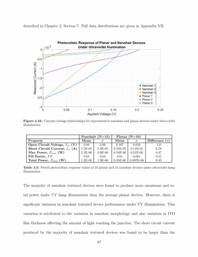
described in Chapter 2, Section 7. Full data distributions are given in Appendix VII.
Figure 4.45: Current/voltage relationships for representative nanohair and planar devices under ultra-violetillumination
Nanohair (N=15) Planar (N=10)Property Mean σ Mean σ Difference (σ)Open Circuit Voltage, Voc (V) 0.09 0.06 0.167 0.016 1.0Short Circuit Current, Isc (A) 1.5E-05 1.4E-05 0.35E-05 0.11E-05 0.79Max Power, Pmax (W) 2.1E-06 3.0E-06 0.58E-06 0.21E-06 0.47Fill Factor, FF 0.55 0.04 0.61 0.081 0.51Total Power, Ptotal (W) 1.2E-06 1.9E-06 0.35E-06 0.097E-06 0.45
Table 4.5: Fitted photovoltaic response values of 10 planar and 15 nanohair devices under ultraviolet lampillumination
The majority of nanohair textured devices were found to produce more maximum and to-
tal power under UV lamp illumination than the average planar devices. However, there is
significant variation in nanohair textured device performance under UV illumination. This
variation is attributed to the variation in nanohair morphology and also variation in ITO
film thickness affecting the amount of light reaching the junction. The short circuit current
produced by the majority of nanohair textured devices was found to be larger than the
87
average planar device. The open circuit voltage was found to be larger in planar devices
than in nanohair textured devices. The fill factors of planar devices was found to be slightly
larger on average. However, the fill factors measured for either device type were found to be
relatively low in comparison to other illumination sources.
The larger short circuit current found in nanohair textured devices suggests that the nanohair
textured devices produce a larger photocurrent than the planar devices. This suggests that
the nanohair textured devices are capable of capturing and converting more incident ultravi-
olet light into electron hole pairs. However, the lower open circuit current found in nanohair
textured devices greatly reduces the overall power output of the devices. The difference in
open circuit voltage is likely due to the larger recombination and shunt resistance effects
found in nanohair textured devices.
The low fill factors of the planar and nanohair textured devices can likely be attributed to
the small photocurrents being produced in the devices. The low production of photocurrent
in either device type can be attributed to the low intensity of the UV light source in addition
to the significant absorption of UV light in the ITO film. As shown in Figure 4.41, this
small photocurrent places the nanohair and planar devices in a region in which recombina-
tion effects are found to be more significant. In the case of nanohair textured devices, shunt
resistance effects are also expected to dominate at these photocurrent values. This has the
effect of reducing the fill factors of either device type to be lower than those found for the
dim solar and blue laser illumination sources.
88
4.3.6 Summary of Device Photovoltaic Response
The optical response of both planar and nanohair textured devices was found to vary under
illumination intensity. This variation in performance resulted from the corresponding pho-
tocurrent. As shown in the dark measurements, the planar devices have a much larger range
of currents in which the current-voltage characteristics are close to the ideal diode charac-
teristics. This lends itself to a much wider range of light intensity under which the planar
devices can be expected to have a decent fill factor, short circuit current, and open circuit
voltage. Both devices perform well under the current ranges seen in blue laser illumination
and reduced solar simulated illumination. However, nanohair devices were found to be more
limited in low intensity light and both devices were found to perform poorly under intense
illumination.
Both the planar and nanohair textured devices are similarly limited in performance under
intense illumination due to series resistance effects. Under intense illumination, both de-
vices produce enough photocurrent such that the short circuit current and fill factor degrade
significantly. The series resistance present in both devices is likely due to inferior electrical
contact or the significant amount of bulk silicon in both devices.
Nanohair textured devices performed worse under low intensity illumination due to greater
recombination effects or shunt leakage effects. The small photocurrents produced by the dim
illumination place the nanohair textured devices in a current range in which recombination
and shunt resistance effects were found to dominate in the dark current-voltage character-
89

istics. This resulted in the degradation of the fill factor and the short circuit current in
nanohair textured devices under these illumination conditions.
Overall, series resistance, surface recombination, and shunt resistance effects limit the effec-
tive range of light intensity under which the nanohair textured devices can operate. Should
the nanohair textured devices be used under typical solar illumination intensities, series re-
sistance effects must be reduced. This can be done readily through modification to the metal
contacts, removal of bulk silicon, or higher bulk silicon doping concentrations. For nanohair
textured devices to perform more effectively under low intensity, surface recombination and
shunt resistance effects must be reduced. This could be accomplished through more effective
passivation of the nanohair surfaces.
The optical response of both planar and nanohair textured devices was also found to vary
under illumination wavelength. Nanohair textured devices were found to be comparable or
slightly more efficient than planar devices under solar simulated, more efficient than planar
devices under blue laser illumination, and more efficient than planar devices under ultravio-
let illumination. This agrees with the assumption that the nanohair texturing will result in
greater high energy light collection. However, the enhanced light trapping effects were found
to be less pronounced for UV illumination, likely because of the significant shunt resistance
effects found at the measured current ranges. These effects could be mitigated by increasing
the intensity of the incident UV light.
The nanohair textured devices inherently have less p-n junction area than the planar devices
90

as a result of nanohair fabrication process. In the absence of any increased light collection
resulting from the nanohair texturing, less p-n junction area should correspond to lower
photocurrent generation, and therefore less power. However, the power generated by the
nanohair textured devices is found to be at least comparable under solar simulated illumina-
tion and significantly larger under blue laser illumination. This suggests that the nanohair
texturing must contribute to greater light collection.
91
REFERENCES
1. T. Ishida, Y. Nakato, ”Structures and properties of electron-beam-evaporated indium
tin oxide films as studied by x-ray photoelectron spectroscopy and work-function mea-
surements”, Journal of Applied Physics, 73, 4344, 1993.
2. R. X. Wang, C. D. Beling, et. al., ”Influence of gaseous annealing environment on
the properties of indium-tin-oxide thin films”, Journal of Applied Physics, 97 033504,
2005.
3. Sorab K. Ghandhi, VLSI Fabrication Principles, John Wiley & Sons Inc., 1994, pgs.
480-481.
4. Zhitong Fan, Daniel J. Ruebusch, et. al., ”Challenges and Prospects of Nanopillar-
Based Solar Cells”, Nano Res, 2, 829-843, 2009.
5. Yaping Dam, Kwanyong Seo, et. al., ”Dramatic Reduction of Surface Recombination
by in Situ Surface Passivation of Silicon Nanowires”, Nano Letters, 11, 2527-2532,
2011.
6. Ya-Ju Lee, Yung-Chi Yao, ”Direct electrical contact of slanted ITO film on axial p-n
junction silicon nanowire solar cells”, OpticsExpress, 21, 2013.
92

CHAPTER 5: CONCLUSIONS
Nanohair textured photovoltaic devices were found to convert light to electron-hole pairs with
comparable or greater efficiency under solar simulated, ultraviolet, blue laser illumination in
comparison to planar devices. This is evidenced by comparable or larger maximum power
output despite the nanohair textured devices having less overall p-n junction area. This is in
agreement with the theory that nanohair texturing should yield greater light collection via
light trapping effects. Additionally, Nanohair texturing was found to yield greater efficiency
gains under blue laser and ultraviolet illumination than found under solar simulated devices
when compared to planar devices. This is in agreement with the theory that higher energy
light collection will improve with through increased greater exposure of the p-n junction.
The photo-response of the top performing nanohair textured device under the considered
illumination sources is given in Figure 5.46 and Figure 5.47. Table 5.6 gives the fitted and
calculated photo-response characteristics for the top performing nanohair textured device.
The energy conversion efficiency of the top performing device was found to be 5.1% under
680W/m2 solar simulated illumination and 10.3% under 13W/m2 solar simulated illumina-
tion. These efficiencies are significantly larger than those previously reported in literature
for similar device architectures. [1] Also, it is very likely that even greater efficiencies can
be achieved through further optimization of this device design.
93

Figure 5.46: Non-illuminated current/voltage characteristics and photo-response of top performingnanohair textured device under 13W/m2 solar simulated, blue laser, and ultraviolet illumination
Figure 5.47: Non-illuminated current/voltage characteristics and photo-response of top performingnanohair textured device under 860W/m2 solar simulated illumination
94

Property Solar (680W/m2) Solar (13W/m2) Blue UltravioletOpen Circuit Voltage, Voc (V) 0.38 0.23 0.21 0.09Short Circuit Current, Isc (A) 3.3E-03 1.5E-04 1.1E-04 6.1E-06Max Power, Pmax (W) 1.3E-03 3.4E-05 2.4E-05 2.4E-07Fill Factor, FF 0.52 0.714 0.707 0.540Total Power, Ptotal (W) 6.5E-04 2.5E-05 1.7E-05 1.3E-07
Table 5.6: Fitted photovoltaic response values of the top performing nanohair textured device under variousillumination sources
Nanohair textured devices were found to have higher series resistance which will limit the
current output of the devices, lowering the efficiency of the devices under intense illumina-
tion, when photocurrent generation rates exceeded a certain threshold. This larger series
resistance found in nanohair textured devices is inherent to it’s structure and may never be
comparable to planar devices. This is because the nanohair texturing reduces the amount
of cross-sectional area through which current can travel through the device, increasing the
series resistance. However, the overall series resistance may still be reduced by removing
excess bulk silicon, increasing substrate doping, and improving ohmic contact to the device.
Therefore, despite the intrinsically larger series resistance of nanohair textured devices, it
may be possible to reduce series resistance enough to result in overall better performance at
high levels of illumination over planar devices, due to enhanced accessibility of the junction
to incident photons in the nanohair textured devices.
Nanohair textured devices were found to exhibit significantly larger surface recombination
and shunt resistance effects than planar devices, which limits the efficiency of the devices
under low intensity illumination. This had the largest impact on the UV illuminated samples
due to the low intensity of the UV source and the heavy absorption of UV light by the indium
tin oxide layer. Recombination effects are expected to be much larger in nanohair textured
95

devices due to the much larger surface area inherent to the nano-textured surface. The larger
surface area results in more empty states present on the silicon surface where electron-hole
pairs can recombine. The extent of this recombination could be reduced through better
passivation of the silicon surface on the nanohair devices.
96

REFERENCES
1. Ya-Ju Lee, Yung-Chi Yao, ”Direct electrical contact of slanted ITO film on axial p-n
junction silicon nanowire solar cells”, OpticsExpress, 21, 2013.
97

CHAPTER 6: FUTURE WORK
Future work should attempt to reduce the effects of the series resistance and surface recom-
bination present in nanohair textured devices in order to improve performance, and achieve
the anticipated benefit over planar devices. Reduced series resistance would expand the
upper range of intensities of light over which the nanohair textured devices can operate ef-
fectively. It is particularly necessary that series resistance effects do not dominate under one
sun illumination in order for nanohair texturing to be viable in solar arrays. Research aiming
to reduce series resistance should focus on investigating better metal contact materials and
methods. The ITO film sheet resistance also contributes to series resistance, and depends on
the location and size of the input/output contact. Additional series resistance reduction is
also possible through the reduction of bulk silicon thickness and/or resistivity in the devices.
Reduction of surface recombination is also necessary to improve performance, and especially
for the lower range of intensities of light over which the nanohair textured devices can op-
erate efficiently. This is critical for the devices to operate effectively in low light conditions.
In order to reduce the surface recombination effects in nanohair textured devices, the states
present at the silicon nanohair surface must be passivated. This could possibly be done via
the thermal oxidation of the silicon nanohair surface, chemical treatment of the surfaces, or
via the deposition of surface passivating material. There is a great deal of published work
on silicon surface passivation, starting in the very early stages of silicon device technology
for silicon wafer surfaces [1,2]. Stable passivation is most affectively achieved by the thermal
oxidation of the silicon surface, which reduces the dangling bonds (and states). Oxidation
98

in steam or post-oxidation steam or hydrogen annealing has been shown to further reduce
surface state densities, due to hydrogen passivation of dangling bonds. High temperature is
not an option for the nanohairs, as we have observed, and even reduced thermal oxidation
proceeds more quickly at the nanoscale, making it difficult to control. Therefore, alterna-
tive low temperature strategies would need to be pursued, such as plasma oxidation, UV
oxidation, chemical oxidation or treatment [3], optimized ALD of Al2O3 [1,2], deposition of
amorphous silicon [4], etc.
Additional research could address the large variability of nanohair texture device perfor-
mance by investigating more reproducible methods of nanohair fabrication. Although the
MACE method of nanohair fabrication was used in the fabrication of this device, achieving
reproducible nanohair structures with this method was often difficult. These variations in
nanohair structures resulted in a far larger variability in device performance over planar
devices due to irregular nanohair morphology and less effective dielectric backfilling. This
makes the investigated MACE nanohair fabrication method relatively low yield in compari-
son to planar devices processes and therefore less desirable for mass manufacturing. Recent
studies report modifications to the MACE process used in this research that could be utilized
for greater nanohair uniformity [5].
99

REFERENCES
1. Yaping Dan, Kwanyong Seo, et. al., ”Dramatic Reduction of Surface Recombination
by in Situ Surface Passivation of Silicon Nanowires”, Nano Letters, 11, 2527-2532,
2011.
2. Paivikki Repo, ”Reducing surface recombination in black silicon photovoltaic devices
using atomic layer deposition”, Aalto University publication series, Doctoral Disserta-
tions, 139/2016.
3. E. Yablonovitch, D. L. AHara, C., et. al., ”Unusually Low Surface-Recombination
Velocity on Silicon and Germanium Surfaces”, Physical Review Letters, 57, 2, 1986.
4. T. Sameshima, K. Sakamoto, et. al., ”Defect reduction and surface passivation of
SiO2/Si by heat treatment with high-pressure H2O vapor”, Applied Physics A, 69,
221-224, 1999.
5. Chia-Yun Chen, Ching-Ping Wong, ”Unveiling the shape-diversified silicon nanowires
made by HF/HNO3 isotropic etching with the assistance of silver”, Nanoscale, 7, 1216,
2015.
100

BIBLIOGRAPHY
1. Chia-Yun Chen, Ching-Ping Wong, ”Unveiling the shape-diversified silicon nanowires
made by HF/HNO3 isotropic etching with the assistance of silver”, Nanoscale, 7, 1216,
2015.
2. Donald A. Neamen, Semiconductor Physics and Devices, McGraw-Hill, New York, New
York, 2003, pgs. 76, 238-250.
3. Edward S. Yang, Fundamentals of Semiconductor Devices, McGraw-Hill Book Com-
pany, 1978, pgs. 147-160.
4. E. Yablonovitch, D. L. AHara, C., et. al., ”Unusually Low Surface-Recombination
Velocity on Silicon and Germanium Surfaces”, Physical Review Letters, 57, 2, 1986.
5. Filmetrics, Refractive Index of Silicon, Si, https://www.filmetrics.com/refractive-index-
database/Si/Silicon
6. John L. Vossen, Werner Kern, Thin Film Processes, Academic Press, New York, New
York, 1978, pgs. 433-480.
7. Junshuai Li, HongYu Yu, ”Aligned Si nanowire-based solar cells”, Nanoscale, 3, 4888,
2011.
8. Kui-Qing Peng, Shuit-Tong Lee, ”Silicon Nanowires for Photovoltaic Solar Energy
Conversion”, Advanced Materials, 27, 198-215, 2011.
9. Paivikki Repo, ”Reducing surface recombination in black silicon photovoltaic devices
101

using atomic layer deposition”, Aalto University publication series, Doctoral Disserta-
tions, 139/2016.
10. R. X. Wang, C. D. Beling, et. al., ”Influence of gaseous annealing environment on
the properties of indium-tin-oxide thin films”, Journal of Applied Physics, 97 033504,
2005.
11. S. M. Sze, Physics of Semiconductor Devices, John Wiley & Sons Inc., Hoboken, New
Jersey, 2007, pgs. 719-725.
12. Sorab K. Ghandhi, VLSI Fabrication Principles, John Wiley & Sons Inc., 1994, pgs.
480-481.
13. T. Ishida, Y. Nakato, ”Structures and properties of electron-beam-evaporated indium
tin oxide films as studied by x-ray photoelectron spectroscopy and work-function mea-
surements”, Journal of Applied Physics, 73, 4344, 1993.
14. T. Sameshima, K. Sakamoto, et. al., ”Defect reduction and surface passivation of
SiO2/Si by heat treatment with high-pressure H2O vapor”, Applied Physics A, 69,
221-224, 1999.
15. Ya-Ju Lee, Yung-Chi Yao, ”Direct electrical contact of slanted ITO film on axial p-n
junction silicon nanowire solar cells”, OpticsExpress, 21, 2013.
16. Yaping Dan, Kwanyong Seo, et. al., ”Dramatic Reduction of Surface Recombination
by in Situ Surface Passivation of Silicon Nanowires”, Nano Letters, 11, 2527-2532,
2011.
102

17. Zachary R. Smith, Rosemary L. Smith, Scott D. Collins, ”Mechanism of Nanowire
Formation in Metal Assisted Chemical Etching”, Electrochimica Acta, 92, 139-147,
2013.
18. Zhipeng Huang, Nadine Geyer, et.al., ”Metal-Assisted Chemical Etching of Silicon: A
Review”, Advanced Materials, 23, 285-308, 2011.
19. Zhitong Fan, Daniel J. Ruebusch, et. al., ”Challenges and Prospects of Nanopillar-
Based Solar Cells”, Nano Res, 2, 829-843, 2009.
103

Appendix I: Nanohair Device Process Flow
1. 1cm x 1cm, 4.85um Si, p-type (100), 1− 2E15cm−3, Boron
BULK Si, 2E14cm−3− 1.3E15cm−3, Phosphorous (100)
2. Piranha clean, 3:1 piranha, 20min, 60C
3. Apply wafer tape mask, subprocedure apply mask
4. Etch nanohairs, subprocedure nanohair etch
5. Submerge masked device in DI, expose masked device to UV lamp, 30min
6. Dry device, nitrogen flow
7. Remove wafer tape mask, scissors
8. Remove silver particles, 30 wt% HNO, 30sec, methanol rinse
9. Dry device, air dry
10. Back-fill nanohairs, subprocedure ALD Al2O3
11. Apply wafer tape mask, subprocedure apply mask
12. Expose nanohair tips, 5 wt% HF etch, 90s, rinse in DI
13. Dry device, nitrogen flow
14. Deposit top electrode, subprocedure magnetron ITO
15. Anneal ITO, tube furnace, 300C, N2 flow, 30min
104

16. Apply wafer tape mask, 2cm x 2cm, wafer tape, center punched hole, 6.3mm in diam-
eter, n-side of device
17. Etch aluminum oxide, drop 49 wt% HF, masked region 20sec, rinse in DI
18. Remove wafer tape mask
19. Apply GaIn paste, exposed n-type Si
20. Apply gold coated substrate, set device GaIn paste down on substrate
105

Subprocedure Apply Mask
1. Apply bottom mask, 2cm x 2cm, wafer tape, to device bottom
2. Apply top mask, 2cm x 2cm, wafer tape, center punched hole, 6.3mm in diameter, to
device top, align with bottom mask
3. Remove trapped air, smooth with flat edge
4. Trim wafer tape edges
Subprocedure Nanohair Etch
1. Silver deposition, 5mMol AgNO3, 4.6Mol HF , 30sec, light stir
2. Rinse in DI
3. Silicon Etch, 1.8Mol H2O2, 4.6Mol HF , 10min, agitated every 20sec
4. Rinse in DI
5. Dry device, nitrogen flow
Subprocedure ALD Al2O3
1. Pre-heat stage to 200C, pump and purge overnight
2. Deposit aluminum oxide, 200C, 1500cycles
(a) TMA dose, 20ms
(b) TMA purge, 2.5sec
106

(c) Water dose, 20ms
(d) Water purge, 4sec
Subprocedure Magnetron ITO
1. Remove native oxide, 5 wt% HF etch, 10sec
2. Rinse in DI
3. Dry with N2
4. ITO deposition, 1um, magnetron sputtering, 3mTorr, 246W, DC, 1.5 Angstroms/sec
(a) Argon, 20sccm, 4min
(b) Argon/Oxygen, 20sccm/4sccm, until end
107

Appendix II: Planar Device Process Flow
1. 1cm x 1cm, 4.85um Si, p-type (100), 1− 2E15cm−3, Boron
BULK Si, 2E14cm−3− 1.3E15cm−3, Phosphorous (100)
2. Piranha clean, 3:1 piranha, 20min, 60C
3. Deposit silicon oxide, subprocedure SiO2 PECVD
4. Apply wafer tape mask, subprocedure apply mask
5. Expose Si surface, 49 wt% HF etch, 30sec
6. Remove wafer tape mask mask, scissors
7. Silicon back-etch, subprocedure silicon back-etch
8. Submerge masked device in DI, expose masked devices to UV lamp, 30min, cut off
mask
9. Remove silicon oxide mask, 49 wt% HF etch, 30sec
10. Dry device, nitrogen flow
11. Passivate Si surface, subprocedure ALD Al2O3
12. Apply mask, subprocedure apply mask
13. Deposit top electrode, subprocedure magnetron ITO
14. Remove wafer tape mask, scissors
15. Anneal ITO, tube furnace, 300C, N2 flow, 30min
108

16. Apply wafer tape mask, n-side of device
17. Etch aluminum oxide, drop 49 wt% HF, masked region 20sec, rinse in DI
18. Dry device, nitrogen flow
19. Remove wafer tape mask, scissors
20. Apply GaIn paste, exposed n-type Si
21. Apply gold coated substrate, set device GaIn paste down on substrate
109

Subprocedure SiO2 PECVD
1. Preheat to 450C
2. Deposit silicon oxide, 1um
Subprocedure Silicon Back-etch
1. Preheat KOH 45 wt% solution to 60C in water bath
2. Etch silicon surface, submerge device in KOH 45 wt% solution, 60C, 6.5 minutes
3. Rinse in DI
4. Dry device, nitrogen flow
Subprocedure ALD Al2O3
1. Pre-heat stage to 200C, pump and purge overnight
2. Deposit aluminum oxide, 200C, 1500cycles
(a) TMA dose, 20ms
(b) TMA purge, 2.5sec
(c) Water dose, 20ms
(d) Water purge, 4sec
Subprocedure Magnetron ITO
1. Remove native oxide, 5 wt% HF etch, 10sec
110

2. Rinse in DI
3. Dry with N2
4. ITO deposition, 1um, magnetron sputtering, 3mTorr, 450W, AC, 1.1 Angstroms/sec
(a) Argon, 20sccm, 4min
(b) Argon/Oxygen, 20sccm/4sccm, until end
111

Appendix III: Device Schematics
Figure 6.48: (a) Side view, (b) top view, and (c) cross-section of nanohair textured photovoltaic device
112

Figure 6.49: (a) Side view, (b) top view, and (c) cross-section of planar photovoltaic device
113

Appendix IV: Stock Solutions
Solution Concentration Maker IDAcetone 99.5 wt% Fisher Chemical A509SK-212Hydrofluoric Acid 48-51 wt% ACROS Organics 223335000Hydrogen Peroxide 30.0-32.0 wt% Fisher Chemical H325-500Methanol 99.8 wt% Fisher Chemical A412-4Nitric Acid 68.0-71.0 wt% Fisher Chemical A18-4Potassium Hydroxide 45 wt% Fisher Chemical SP236-4Silver Nitrate Crystal Spectrum Chemical MFG Corp. S1086Sulfuric Acid 95.0-98.0 wt% Fisher Chemical A300S-212
114

Appendix V: Equipment
Equipment Maker ModelAtomic Layer Deposition System Oxford Instruments OpAlBlue Laser ThorLabs CPS405Contact Profilometer KLA Tencor Alpha-Step 500Ellipsometer J. A. Woollam Co., Inc M-2000VHemispherical Energy Analyzer SPECS PHOIBOS HSA3000 MCD5Magnetron Sputtering System AJA International Inc. ATC 2000-VOptical Profilometer FRT MircoProf 100Parylene Deposition System Specialty Coating Systems PDS 2010Plasma Enhanced Chemical Vapor Deposition System Oxford Instruments Plasmalab80PlusScanning Electron Microscope Ziess NVision 40Semiconductor Parametric Analyzer Keithley 4200-SCSSolar Emulator Newport LCS-100Thin-film Analyzer Filmetrics F40-UVUV Lamp UVP UVL-21UV-Visible Light Source OceanOptics DH-2000-BALUV-Visible Spectrometer OceanOptics USB400
115
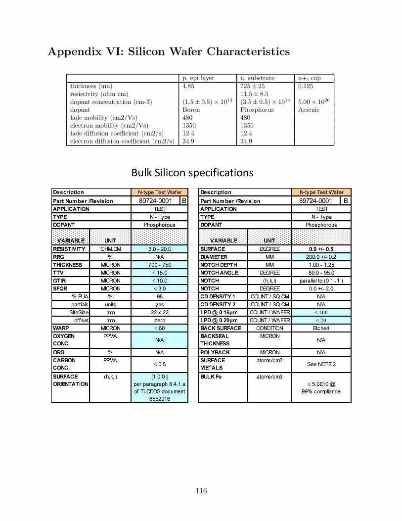
Appendix VI: Silicon Wafer Characteristics
p, epi layer n, substrate n+, capthickness (um) 4.85 725± 25 0.125resistivity (ohm cm) 11.5± 8.5dopant concentration (cm-3) (1.5± 0.5)× 1015 (3.5± 0.5)× 1014 5.00× 10²⁰
dopant Boron Phosphorus Arsenichole mobility (cm2/Vs) 480 480electron mobility (cm2/Vs) 1350 1350hole diffusion coefficient (cm2/s) 12.4 12.4electron diffusion coefficient (cm2/s) 34.9 34.9
116
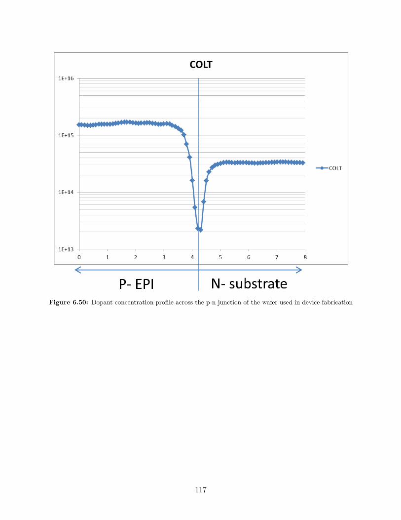
Figure 6.50: Dopant concentration profile across the p-n junction of the wafer used in device fabrication
117

Figure 6.51: Dopant concentration profile of the n+ silicon cap of the wafer used in device fabrication
118
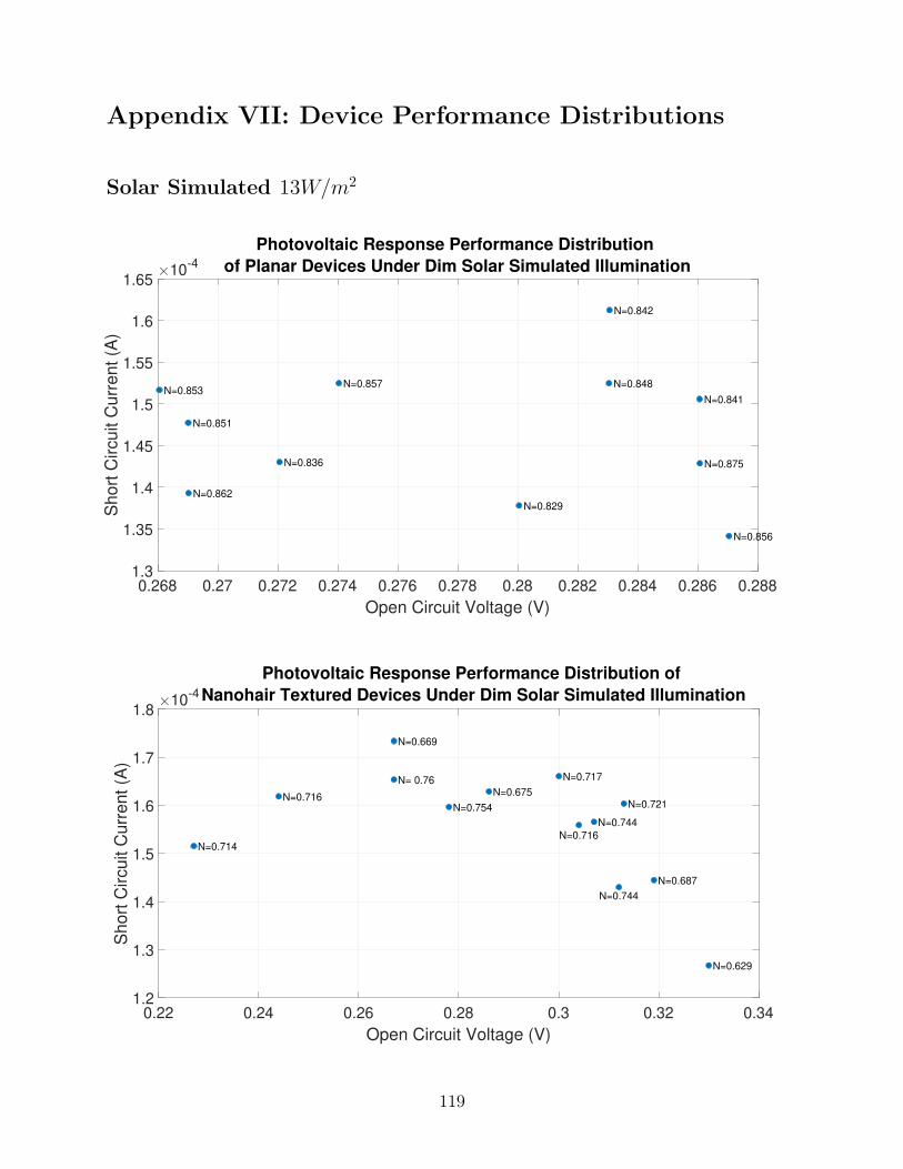
Appendix VII: Device Performance Distributions
Solar Simulated 13W/m2
0.268 0.27 0.272 0.274 0.276 0.278 0.28 0.282 0.284 0.286 0.288
Open Circuit Voltage (V)
1.3
1.35
1.4
1.45
1.5
1.55
1.6
1.65
Short
Circuit C
urr
ent (A
)
10-4
Photovoltaic Response Performance Distribution
of Planar Devices Under Dim Solar Simulated Illumination
N=0.856
N=0.842
N=0.853
N=0.862
N=0.857
N=0.841
N=0.848
N=0.829
N=0.875
N=0.851
N=0.836
0.22 0.24 0.26 0.28 0.3 0.32 0.34
Open Circuit Voltage (V)
1.2
1.3
1.4
1.5
1.6
1.7
1.8
Short
Circuit C
urr
ent (A
)
10-4
Photovoltaic Response Performance Distribution of
Nanohair Textured Devices Under Dim Solar Simulated Illumination
N=0.714
N=0.717
N=0.716
N= 0.76
N=0.744
N=0.716
N=0.687
N=0.629
N=0.721
N=0.744
N=0.754
N=0.669
N=0.675
119

Blue Laser
0.09 0.1 0.11 0.12 0.13 0.14 0.15 0.16
Open Circuit Voltage (V)
2
4
6
8
10
12
Short
Circuit C
urr
ent (A
)
10-6
Photovoltaic Response Performance Distribution
of Planar Devices Under Blue Illumination
N=0.792
N=0.791N=0.796
N= 0.77N=0.727
N=0.738
N=0.735
N=0.567
N=0.722N=0.775N= 0.73N=0.689
N= 0.66
0 0.05 0.1 0.15 0.2 0.25
Open Circuit Voltage (V)
0
0.2
0.4
0.6
0.8
1
1.2
Short
Circuit C
urr
ent (A
)
10-4
Photovoltaic Response Performance Distribution of
Nanohair Textured Devices Under Blue Illumination
N=0.708
N=0.673
N=0.636
N=0.721N= 0.68N=0.617
N=0.579N= 0.62
N=0.539N=0.532N=0.523
N=0.524N=0.536N=0.528
N=0.559
120
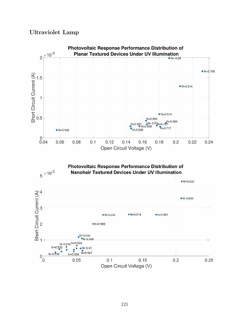
Ultraviolet Lamp
0.04 0.06 0.08 0.1 0.12 0.14 0.16 0.18 0.2 0.22 0.24
Open Circuit Voltage (V)
0
0.5
1
1.5
2
Short
Circuit C
urr
ent (A
)
10-5
Photovoltaic Response Performance Distribution of
Planar Textured Devices Under UV IlluminationN= 0.58
N=0.493
N= 0.57N=0.597
N=0.542 N=0.636
N=0.656
N=0.584N=0.727
N=0.514
N=0.514
N=0.717
N=0.706
121
BIOGRAPHY OF THE AUTHOR
Michael Small was born in Iron Mountain, Michigan on April 28th, 1992. He grew up in
the nearby town of Norway, Michigan and graduated from Norway High School in 2010.
He attended Michigan Technological University in Houghton, Michigan where he graduated
with a Bachelor’s of Science in Applied Physics in the Fall of 2015. Immediately afterwards,
he joined the Physics and Astronomy Department at the University of Maine, Orono, in
pursuit of a Master’s of Engineering Degree in Engineering Physics. Following the completion
of his degree, Michael will be joining Intel Co. to begin his career in the semiconductor
device fabrication industry. Michael is a candidate for the Master of Engineering degree in
Engineering Physics from the University of Maine in December 2018.
122


![Highly textured silicon [111 ... - Solar-Tectic LLC · Highly textured silicon [111] crystalline thin-film on buffered soda-lime glass by e-beam evaporation Shane McMahona, Ashok](https://img.pdfslide.us/doc/110x75/600fc27a2a567a149c76fd98/highly-textured-silicon-111-solar-tectic-highly-textured-silicon-111-crystalline.jpg)


![Passivation of Textured Silicon Wafers:Influence of Pyramid Size … · 2017. 1. 16. · IPA-free KOH containing solution influences the pyramid morphology [8,9]. Largest pyramids](https://img.pdfslide.us/doc/110x75/5ff2912062019c53bf06933e/passivation-of-textured-silicon-wafersinfluence-of-pyramid-size-2017-1-16.jpg)