Embed Size (px)
Citation preview
Application of Fuzzy Integrated FMEA with Product Lifetime Consideration for New ProductDevelopment in Flexible Electronics Industry
Pun, Kelvin P.L.; Rotanson, Jason; Cheung, Chee-Wah; Chan, Alan H.S.
Published in:Journal of Industrial Engineering and Management
Published: 01/04/2019
Document Version:Final Published version, also known as Publisher’s PDF, Publisher’s Final version or Version of Record
License:CC BY-NC
Publication record in CityU Scholars:Go to record
Published version (DOI):10.3926/jiem.2765
Publication details:Pun, K. P. L., Rotanson, J., Cheung, C-W., & Chan, A. H. S. (2019). Application of Fuzzy Integrated FMEA withProduct Lifetime Consideration for New Product Development in Flexible Electronics Industry. Journal ofIndustrial Engineering and Management, 12(1), 176-200. https://doi.org/10.3926/jiem.2765
Citing this paperPlease note that where the full-text provided on CityU Scholars is the Post-print version (also known as Accepted AuthorManuscript, Peer-reviewed or Author Final version), it may differ from the Final Published version. When citing, ensure thatyou check and use the publisher's definitive version for pagination and other details.
General rightsCopyright for the publications made accessible via the CityU Scholars portal is retained by the author(s) and/or othercopyright owners and it is a condition of accessing these publications that users recognise and abide by the legalrequirements associated with these rights. Users may not further distribute the material or use it for any profit-making activityor commercial gain.Publisher permissionPermission for previously published items are in accordance with publisher's copyright policies sourced from the SHERPARoMEO database. Links to full text versions (either Published or Post-print) are only available if corresponding publishersallow open access.
Take down policyContact [email protected] if you believe that this document breaches copyright and provide us with details. We willremove access to the work immediately and investigate your claim.
Download date: 11/02/2022
Journal of Industrial Engineering and ManagementJIEM, 2019 – 12(1): 176-200 – Online ISSN: 2013-0953 – Print ISSN: 2013-8423
https://doi.org/10.3926/jiem.2765
Application of Fuzzy Integrated FMEA with Product Lifetime Considerationfor New Product Development in Flexible Electronics Industry
Kelvin P.L. Pun1,2 , Jason Rotanson2 , Chee-Wah Cheung2 , Alan H.S. Chan1
1Department of SEEM, City University of Hong Kong (Hong Kong)2Compass Technology Co Ltd (Hong Kong)
[email protected], [email protected], [email protected], [email protected]
Received: October 2018Accepted: January 2019
Abstract:
Purpose: the aim of this paper is to minimize the risks of new product development and shortentime-to-market, particularly for high-tech enterprise where the complexity of the product generates vastamount of failure mode.
Design/methodology/approach: first, the concept of Critical Consideration Factor (CCF) is introducedbased on product-specific technical characteristics, expected lifetime, and yield requirement to identify andprioritize the critical failure mode in the subsequent Failure Mode and Effect Analysis (FMEA), followedby process characterization on the high-risk failure mode and Critical Parameter Management (CPM)practice to realize a robust mass production system of the developed technology. The application on thedevelopment of advanced flexible substrate and surface finishes fabrication technique is presented.
Findings: through the proposed methodology, the risk level of each potential failure mode can beaccurately quantified to identify the critical variables. With process characterization, reliability of theproduct is ensured. Consequently, significant reduction in development resources and time-to-market canbe achieved.
Practical implications: the development strategy allows high tech enterprises to achieve a balancedecosystem in which value created through adaption of new technology/product can be thoroughlycaptured through commercialization in a timely manner with no field failure.
Originality/value: the proposed development strategy utilizes a unique approach with thoroughconsiderations that enables high tech enterprise to deliver new product with rapid time-to-market withoutsacrificing product lifetime reliability, which is key to achieve competitive advantage in the highly dynamicmarket.
Keywords: new product development, risk management, failure mode and effect analysis, critical parametermanagement, advanced manufacturing, industry 4.0
To cite this article:
Pun, K.P.L., Rotanson, J., Cheung, C., & Chan, A.H.S. (2019). Application of fuzzy integrated FMEA with product lifetime consideration for new product development in flexible electronics industry. Journal of Industrial Engineering and Management, 12(1), 176-200. https://doi.org/10.3926/jiem.2765
-176-
Journal of Industrial Engineering and Management – https://doi.org/10.3926/jiem.2765
1. Introduction1.1. New Product Development
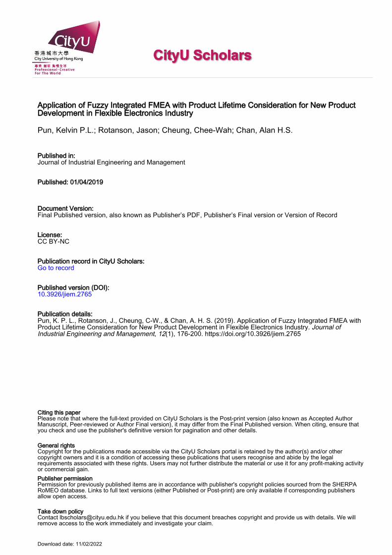
To remain sustainable and profitable, high tech enterprises face multiple challenges in competitive businessenvironments and rapid changes in market demand. One of the key success factors is continuous investment inR&D to create value by commercializing technology into products, setting industry standards, and effectivelydeterring the entry of rivals (Zahra, 1996). With ever increasing customer expectations, time becomes the criticalfactor in the development of new technology. Manufacturers are required to achieve short development cycles andconsequently time-to-market, while simultaneously offering cost advantages and scalability. Opportunities fromNPD also incur huge risks, in which unpredictable obstacles can arise during mass production that lead to unstableyield loss and impede product commercialization. Managing NPD is a vital and challenging process, as it involvesextensive financial and human resources (Bhuiyan, 2011). In fact, a considerable number of products never make itto the market, with a failure rate of 25% to 45% (Mosley, 1994; Crawford, 1987). Avoiding failure is paramount inthe development of technical products. The earlier the failure detection, the more economic loss can be avoided(Figure 1) and the faster commercialization can be achieved (Würtenberger, Kloberdanz, Lotz & Von Ahsen, 2014).In addition to the cost, commercialized products that experience field failure during their product lifetime willnegatively affect customer experience, not to mention possible liability issue. Therefore, solving these unforeseeableproblems is critical to achieve successful technology transfer. Indeed, organizations need to employ a multi-dimensional development strategy to ensure that the value created is in equilibrium with the value captured (Rajan,2016).
Figure 1. Cost per failure that increase logarithmically at differentdevelopment stage (Würtenberger et al., 2014)
Success of the NPD process requires synergy from cross-functional teams, management support, and conduciveorganizational structure to achieve the desired product performance, speed to market, and development cost(Schimmoeller, 2010). Quality improvement tools, such as quality function deployment (QFD), benchmarking,conjoint analysis, and FMEA have been investigated by previous researchers. FMEA in particular, has been usedin numerous development strategy frameworks. For example, Belu, Rachieru, Militaru & Anghel (2012)demonstrated the application of design FMEA with functional analysis in new product development stage.
-177-
Journal of Industrial Engineering and Management – https://doi.org/10.3926/jiem.2765
Doğan and Cebeci (2016) integrated the use of QFD to generate FMEA based on customer requirement inNPD process. These studies, despite being able to detect possible risks beforehand, do not ensure a robustsystem that is ready for mass production while taking into account product lifetime reliability. Natarajan, Senthil,Devadasan, Mohan and Sivaram (2013) implemented quality and reliability on to new product developmentprocess, however the methodology presented is not quantitative as it focuses on systematically achieving certainmilestone on the product development. Moreover, methodology in traditional FMEA is highly debatable due tothe subjective rating as well as questionable weighting and calculation formula. Various methods have beenproposed to improve FMEA such as using grey relational analysis and fuzzy logic based on safety, quality, andcost (Baynal, Sari & Akpinar, 2018; Banduka, Tadić, Mačužić and Crnjac, 2018). Therefore, there is a need fornovel development strategy based on FMEA that takes into account product quality & reliability from thetechnical aspect through quantitative analysis to intelligently manage and optimize development resources toreduce development time.
1.2. The Flexible Electronics Industry
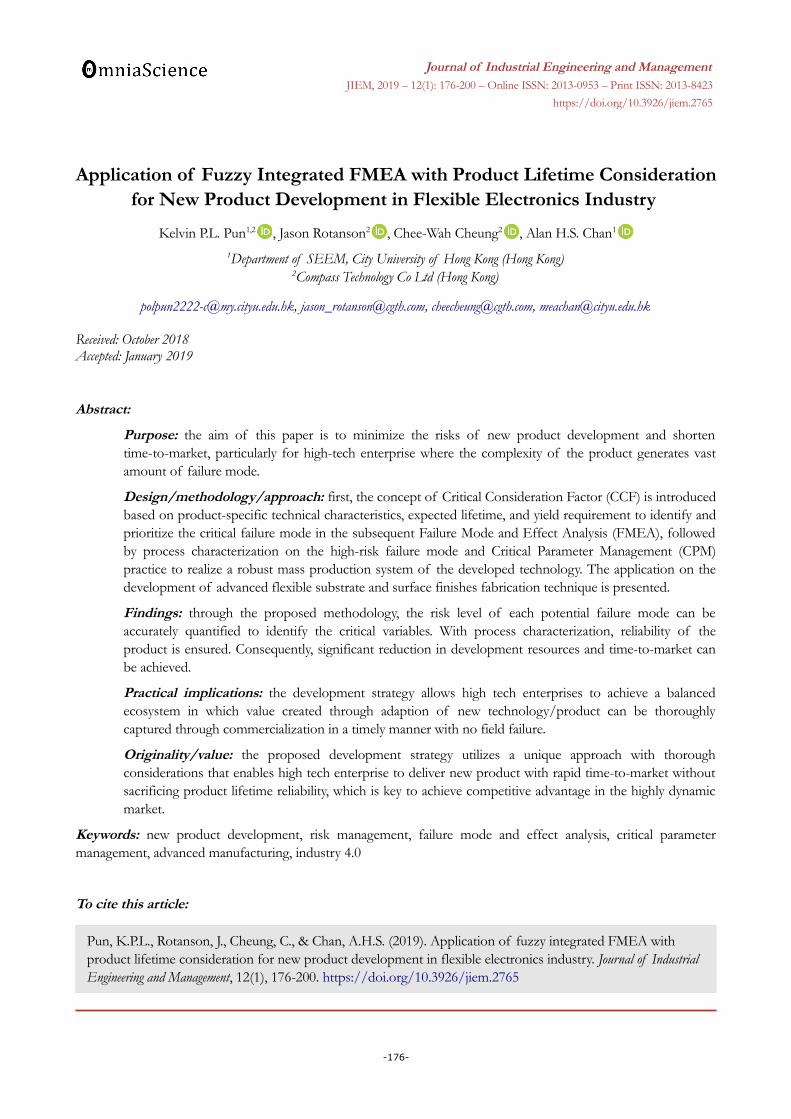
Increasing demand for advanced electronic products with a smaller form factor, multi-functionality, higherperformance, and lower overall cost has driven the semiconductor industry to continuously innovate emergingadvanced packaging technologies using flexible substrates. The electronic packaging field constitutes a highlysophisticated area that necessitates specific expertise on numerous levels. Choosing the optimal process equipmentand materials, combined with innovative design solutions that address thermal, mechanical, and electrical issues willbe the key success factors. Figure 2 shows the construction of an advanced electronic package with heterogeneousintegration. From top to bottom, the package consists of die (integrated circuit/ IC)/component, IC levelinterconnect, package level interconnect (1st level), substrate, board level interconnect (2nd level), and the mainboard itself.
Figure 2. Heterogeneous integration in an advanced electronic package(Pun, Islam, Rotanson, Cheung & Chan, 2018a)
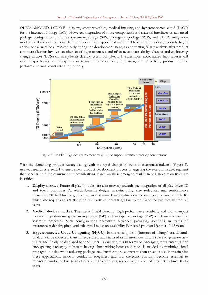
With such heterogeneity in a microsystem, various components are integrated by different kinds of materials andinterfaces in a compact space. The reaction between these materials and the environment determinesmanufacturability, functionality, and reliability. With the extant trend that is shifting towards the “More thanMoore” law, 3D IC integration using through silicon via (TSV) has been developed for higher density andshorter signal propagation (Pangracious, Marrakchi & Mehrez, 2015). To enable this, packaging substrate isessential to fan out the compact circuitries between the 3D IC module and the main board, so that thermalexpansion mismatch can be minimized, and a less dense main board is required (lower cost) (Lau, 2015).Moreover, scaling of silicon devices is reaching its physical limit (Nawrocki, 2010). Interconnect technology isalso growing at a rapid pace (Figure 3). Therefore, diversification of semiconductor products is predicted tocreate new competition in advanced packaging substrates and their interconnect technologies. Advancedpackaging will be the critical enabler of a wide variety of devices in many applications, such as
-178-
Journal of Industrial Engineering and Management – https://doi.org/10.3926/jiem.2765
OLED/AMOLED, LCD/TFT displays, smart wearables, medical imaging, and hyperconnected cloud (HyCC)for the internet of things (IoTs). However, integration of more components and material interfaces on advancedpackage configurations, such as system-in-package (SiP), package-on-package (PoP), and 3D IC integrationmodules will increase potential failure modes in an exponential manner. These failure modes (especially highlycritical ones) must be eliminated early during the development stage, as conducting failure analysis after productcommercialization involves another set of huge resources, and often necessitates design changes and engineeringchange notices (ECN) on many levels due to system complexity. Furthermore, encountered field failures willincur major losses for enterprises in terms of liability, cost, reputation, etc. Therefore, product lifetimeperformance must constitute a top priority.
Figure 3. Trend of high-density interconnect (HDI) to support advanced package development
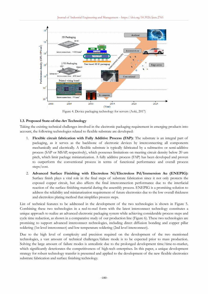
With the demanding product features, along with the rapid change of trend in electronics industry (Figure 4),market research is essential to ensure new product development process is targeting the relevant market segmentthat benefits both the consumer and organizations. Based on these emerging market trends, three main fields areidentified:
1. Display market: Future display modules are also moving towards the integration of display driver ICand touch controller IC, which benefits design, manufacturing, size reduction, and performance(Synaptics, 2014). This integration means that more functionalities can be incorporated into a single IC,which also requires a COF (Chip-on-film) with an increasingly finer pitch. Expected product lifetime: <5years.
2. Medical devices market: The medical field demands high performance reliability and ultra-compactmodule integration using system in package (SiP) and package on package (PoP) which involve multipleassembly processes. Such configurations necessitate advanced packaging solutions, in terms ofinterconnect density, pitch, and substrate line/space scalability. Expected product lifetime: 10-15 years.
3. Hyperconnected Cloud Computing (HyCC): In the coming IoTs (Internet of Things) era, all kindsof data will be collected, transmitted, stored, and analysed in an enormous virtual space to generate newvalues and finally be displayed for end users. Translating this in terms of packaging requirement, a fineline/spacing packaging substrate having short wiring between devices is needed to minimize signalpropagation delay while reducing package size. Furthermore, as transmission speed is also increasing forthese applications, smooth conductor roughness and low dielectric constant become essential tominimize conductor loss (skin effect) and dielectric loss, respectively. Expected product lifetime: 10-15years.
-179-
Journal of Industrial Engineering and Management – https://doi.org/10.3926/jiem.2765
Figure 4. Device packaging technology for servers (Aoki, 2017)
1.3. Proposed State-of-the-Art Technology
Taking the existing technical challenges involved in the electronic packaging requirement in emerging products intoaccount, the following technologies related to flexible substrate are developed:
1. Flexible circuit fabrication with Fully Additive Process (FAP): The substrate is an integral part ofpackaging, as it serves as the backbone of electronic devices by interconnecting all componentsmechanically and electrically. A flexible substrate is typically fabricated by a subtractive or semi-additiveprocess (SAP or MSAP, respectively), which possesses limitations on meeting circuit density below 20 umpitch, which limit package miniaturization. A fully additive process (FAP) has been developed and provento outperform the conventional process in terms of functional performance and overall processsteps/cost.
2. Advanced Surface Finishing with Electroless Ni/Electroless Pd/Immersion Au (ENEPIG):Surface finish plays a vital role in the final steps of substrate fabrication since it not only protects theexposed copper circuit, but also affects the final interconnection performance due to the interfacialreaction of the surface finishing material during the assembly process. ENEPIG is a promising solution toaddress the reliability and miniaturization requirement of future electronics due to the low overall thicknessand electroless plating method that simplifies process steps.
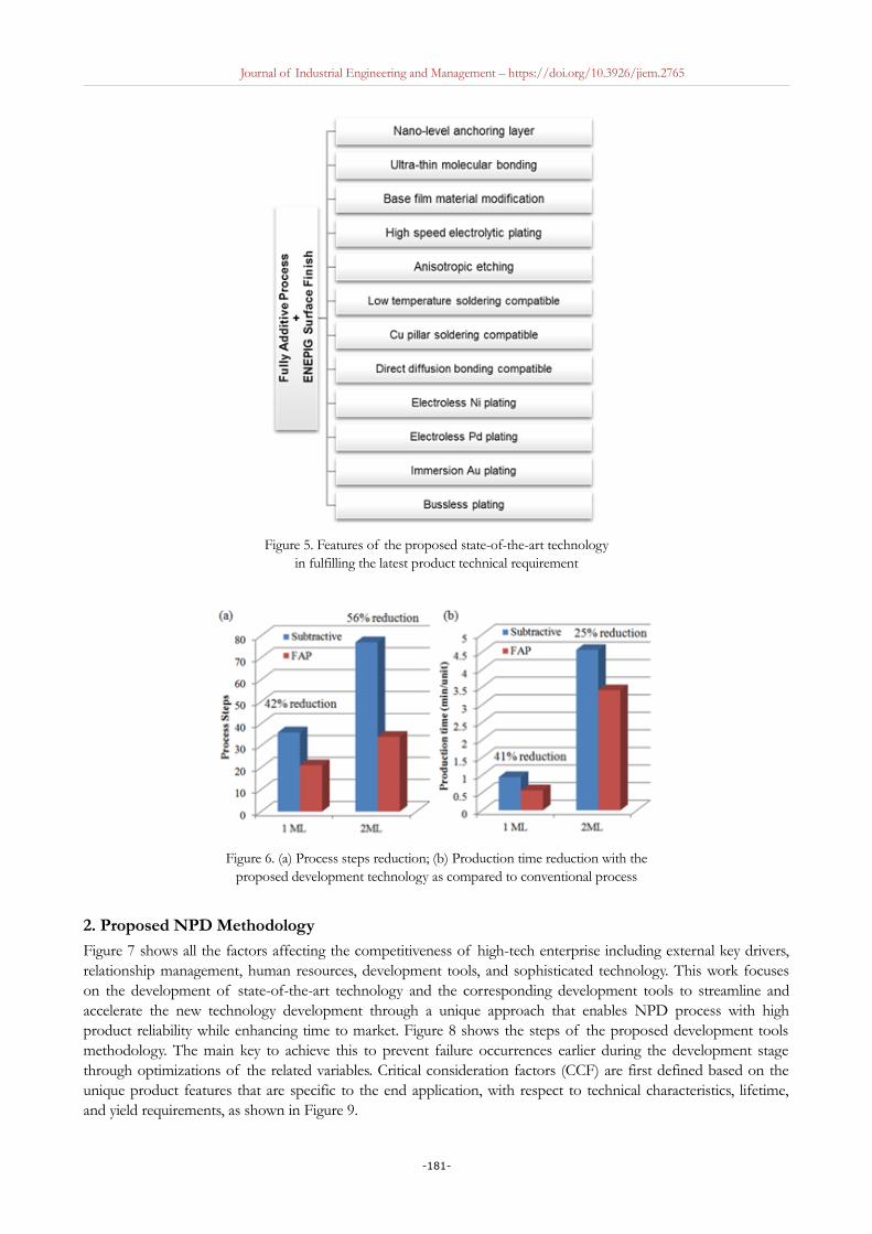
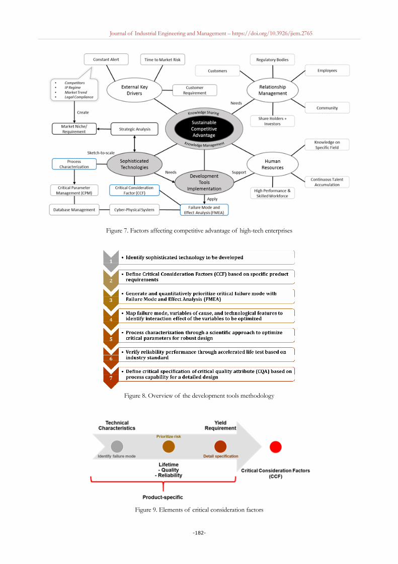
List of technical features to be addressed in the development of the two technologies is shown in Figure 5.Combining these two technologies in a reel-to-reel form with the latest interconnect technology constitutes aunique approach to realize an advanced electronic packaging system while achieving considerable process steps andcycle time reduction, as shown in a comparative study of our production line (Figure 6). These two technologies arepromising to support advanced interconnect technologies, including direct diffusion bonding and copper pillarsoldering (1st level interconnect) and low temperature soldering (2nd level interconnect).
Due to the high level of complexity and precision required on the development of the two mentionedtechnologies, a vast amount of technical challenges/failure mode is to be expected prior to mass production.Solving the large amount of failure modes is unrealistic due to the prolonged development time/time-to-market,which significantly deteriorates the competitiveness of high-tech enterprises. In this paper, a unique developmentstrategy for robust technology transfer is presented and applied to the development of the new flexible electronicssubstrate fabrication and surface finishing technology.
-180-
Journal of Industrial Engineering and Management – https://doi.org/10.3926/jiem.2765
Figure 5. Features of the proposed state-of-the-art technologyin fulfilling the latest product technical requirement
Figure 6. (a) Process steps reduction; (b) Production time reduction with theproposed development technology as compared to conventional process
2. Proposed NPD Methodology
Figure 7 shows all the factors affecting the competitiveness of high-tech enterprise including external key drivers,relationship management, human resources, development tools, and sophisticated technology. This work focuseson the development of state-of-the-art technology and the corresponding development tools to streamline andaccelerate the new technology development through a unique approach that enables NPD process with highproduct reliability while enhancing time to market. Figure 8 shows the steps of the proposed development toolsmethodology. The main key to achieve this to prevent failure occurrences earlier during the development stagethrough optimizations of the related variables. Critical consideration factors (CCF) are first defined based on theunique product features that are specific to the end application, with respect to technical characteristics, lifetime,and yield requirements, as shown in Figure 9.
-181-
Journal of Industrial Engineering and Management – https://doi.org/10.3926/jiem.2765
Figure 7. Factors affecting competitive advantage of high-tech enterprises
Figure 8. Overview of the development tools methodology
Figure 9. Elements of critical consideration factors
-182-
Journal of Industrial Engineering and Management – https://doi.org/10.3926/jiem.2765
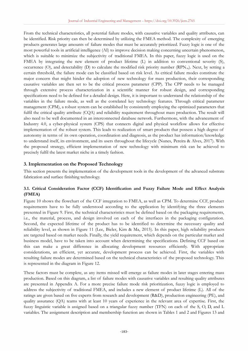
From the technical characteristics, all potential failure modes, with causative variables and quality attributes, canbe identified. Risk priority can then be determined by utilizing the FMEA method. The complexity of emergingproducts generates large amounts of failure modes that must be accurately prioritized. Fuzzy logic is one of themost powerful tools in artificial intelligence (AI) to improve decision making concerning uncertain phenomenon,which is suitable to minimize the subjectivity of traditional FMEA. In this paper, fuzzy logic is used on theFMEA by integrating the new element of product lifetime (L) in addition to conventional severity (S),occurrence (O), and detectability (D) to calculate the modified risk priority number (RPNm). Next, by setting acertain threshold, the failure mode can be classified based on risk level. As critical failure modes constitute themajor concern that might hinder the adoption of new technology for mass production, their correspondingcausative variables are then set to be the critical process parameter (CPP). The CPP needs to be managedthrough extensive process characterization in a scientific manner for robust design, and correspondingspecifications need to be defined for a detailed design. Here, it is important to understand the relationship of thevariables in the failure mode, as well as the correlated key technology features. Through critical parametermanagement (CPM), a robust system can be established by consistently employing the optimized parameters thatfulfil the critical quality attribute (CQA) and reliability requirement throughout mass production. The result willalso need to be well documented in an interconnected database network. Furthermore, with the advancement ofIndustry 4.0, a cyber-physical system (CPS) that connects digital and physical workflow allows for effectiveimplementation of the robust system. This leads to realization of smart products that possess a high degree ofautonomy in terms of its own operation, coordination and diagnosis, as the product has information/knowledgeto understand itself, its environment, and its users throughout the lifecycle (Nunes, Pereira & Alves, 2017). Withthe proposed strategy, efficient implementation of new technology with minimum risk can be achieved toprecisely fulfil the latest market niche in a timely fashion.
3. Implementation on the Proposed Technology
This section presents the implementation of the development tools in the development of the advanced substratefabrication and surface finishing technology.
3.1. Critical Consideration Factor (CCF) Identification and Fuzzy Failure Mode and Effect Analysis(FMEA)
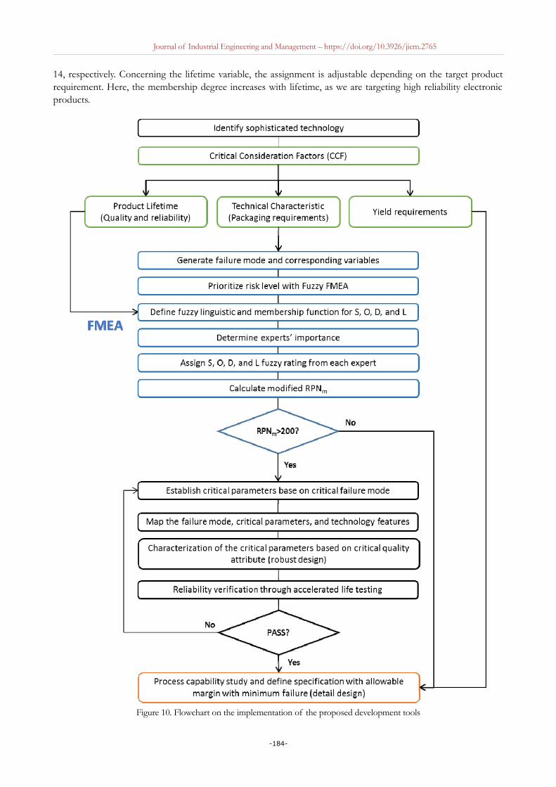
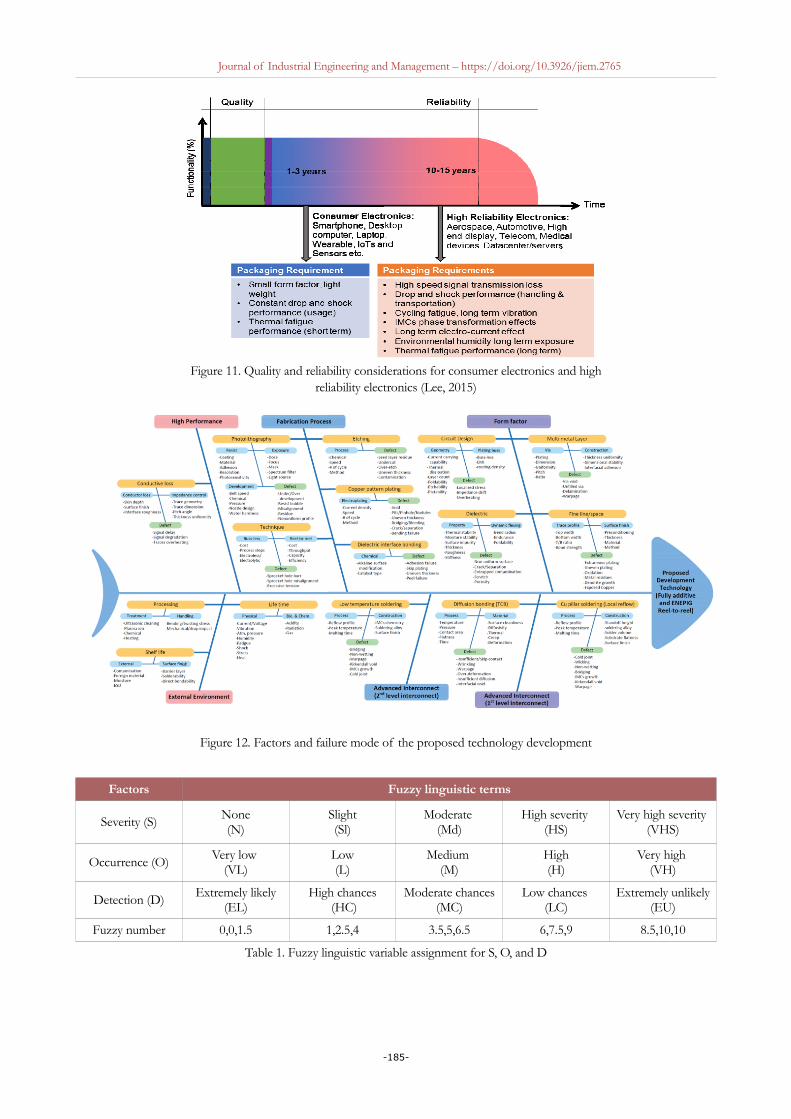
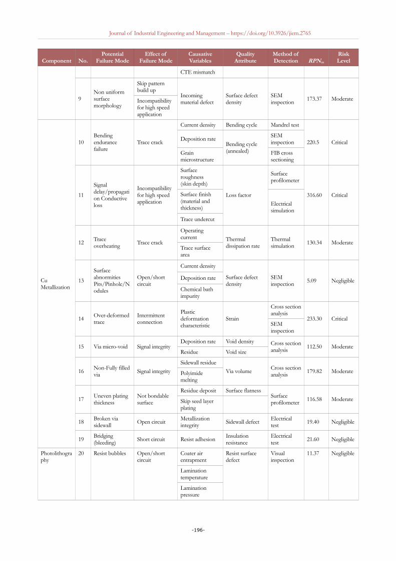
Figure 10 shows the flowchart of the CCF integration to FMEA, as well as CPM. To determine CCF, productrequirements have to be fully understood according to the application by identifying the three elementspresented in Figure 9. First, the technical characteristics must be defined based on the packaging requirements,i.e., the material, process, and design involved on each of the interfaces in the packaging configuration.Second, the expected lifetime of the product has to be identified to determine the necessary quality andreliability level, as shown in Figure 11 (Lee, Bieler, Kim & Ma, 2015). In this paper, high reliability productsare targeted based on market needs. Finally, the yield requirement, which depends on the particular market andbusiness model, have to be taken into account when determining the specifications. Defining CCF based onthis can make a great difference in allocating development resources efficiently. With appropriateconsiderations, an efficient, yet accurate, development process can be achieved. First, the variables withresulting failure modes are determined based on the technical characteristics of the proposed technology. Thisis represented in the diagram in Figure 12.
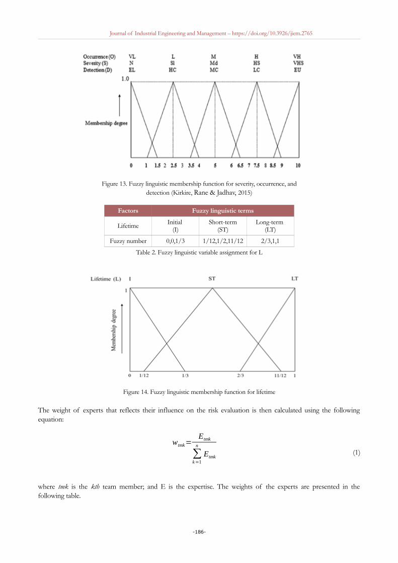
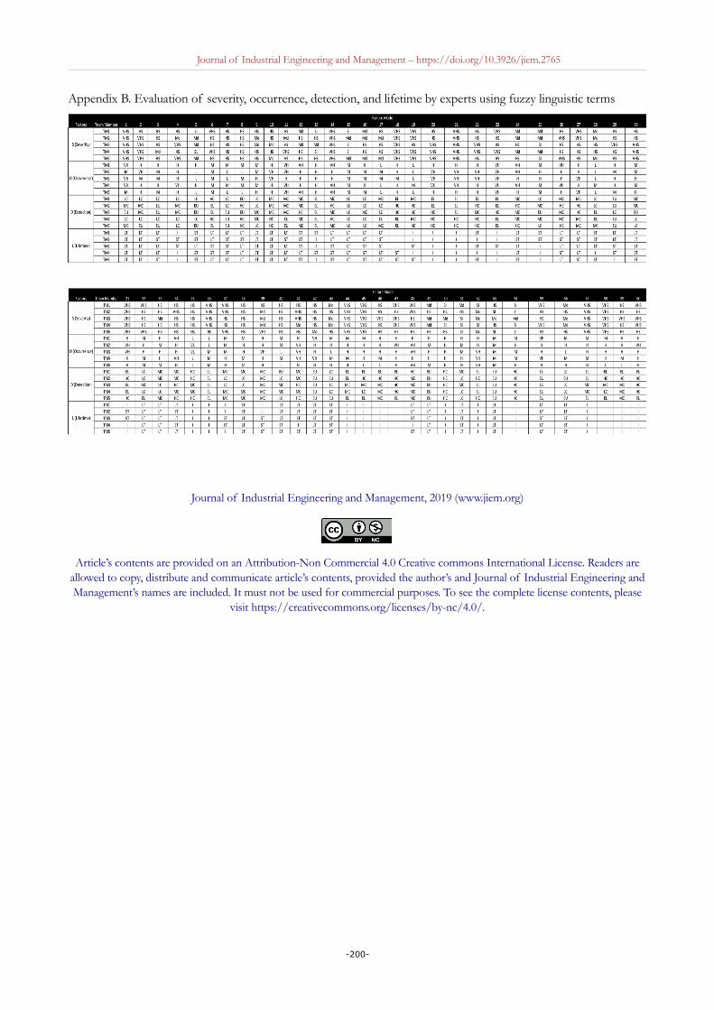
These factors must be complete, as any items missed will emerge as failure modes in later stages entering massproduction. Based on this diagram, a list of failure modes with causative variables and resulting quality attributesare presented in Appendix A. For a more precise failure mode risk prioritization, fuzzy logic is employed toaddress the subjectivity of traditional FMEA, and includes a new element of product lifetime (L). All of theratings are given based on five experts from research and development (R&D), production engineering (PE), andquality assurance (QA) teams with at least 10 years of experience in the relevant area of expertise. First, thefuzzy linguistic variable is assigned based on a triangular fuzzy number (TFN) on each of the S, O, D, and Lvariables. The assignment description and membership function are shown in Tables 1 and 2 and Figures 13 and
-183-
Journal of Industrial Engineering and Management – https://doi.org/10.3926/jiem.2765
14, respectively. Concerning the lifetime variable, the assignment is adjustable depending on the target productrequirement. Here, the membership degree increases with lifetime, as we are targeting high reliability electronicproducts.
Figure 10. Flowchart on the implementation of the proposed development tools
-184-
Journal of Industrial Engineering and Management – https://doi.org/10.3926/jiem.2765
Figure 11. Quality and reliability considerations for consumer electronics and highreliability electronics (Lee, 2015)
Figure 12. Factors and failure mode of the proposed technology development
Factors Fuzzy linguistic terms
Severity (S) None(N)
Slight(Sl)
Moderate (Md)
High severity (HS)
Very high severity (VHS)
Occurrence (O) Very low (VL)
Low(L)
Medium (M)
High(H)
Very high (VH)
Detection (D) Extremely likely(EL)
High chances (HC)
Moderate chances(MC)
Low chances (LC)
Extremely unlikely(EU)
Fuzzy number 0,0,1.5 1,2.5,4 3.5,5,6.5 6,7.5,9 8.5,10,10
Table 1. Fuzzy linguistic variable assignment for S, O, and D
-185-
Journal of Industrial Engineering and Management – https://doi.org/10.3926/jiem.2765
Figure 13. Fuzzy linguistic membership function for severity, occurrence, anddetection (Kirkire, Rane & Jadhav, 2015)
Factors Fuzzy linguistic terms
Lifetime Initial (I)
Short-term(ST)
Long-term (LT)
Fuzzy number 0,0,1/3 1/12,1/2,11/12 2/3,1,1
Table 2. Fuzzy linguistic variable assignment for L
Figure 14. Fuzzy linguistic membership function for lifetime
The weight of experts that reflects their influence on the risk evaluation is then calculated using the followingequation:
wtmk=Etmk
∑k=1
n
Etmk (1)
where tmk is the kth team member; and E is the expertise. The weights of the experts are presented in thefollowing table.
-186-

Journal of Industrial Engineering and Management – https://doi.org/10.3926/jiem.2765
Team member 1 2 3 4 5
Weight 0.3 0.25 0.2 0.15 0.1
Table 3. Weight assignment of each team member
Assignment of the fuzzy linguistic variable is shown in Appendix B. The fuzzy linguistic terms are calculated basedon the methodology developed by Kirkire et al (2015), as shown in the following:
S ijn=(SL ij
n , SM ijn ,SU ij
n ) , S ijn ∈T ,
where0≤SL ij
n≤SM ijn≤SU ij
n≤10(2)
O ijn =(OL ij
n ,OM ijn , OU ij
n ) ,O ijn ∈T ,
where0≤OL ij
n≤OM ijn ≤OU ij
n≤10(3)
D ijn=(DL ij
n , DM ijn ,DU ij
n ) , Dijn ∈T ,
where0≤DL ij
n≤DM ijn≤DU ij
n≤10(4)
L ijn =(L L ij
n , LM ijn , LU ij
n ) , L ijn ∈S ,
where0≤L L ij
n≤LM ijn≤LU ij
n≤1(5)
S ij=S ij1 x W tm 1+S ij
2 x W tm 2+ ...+S ijn x W tmn (6)
O ij=O ij1 x W tm 1+O ij
2 x W tm 2+ ...+O ijn x W tmn (7)
D ij=Dij1 x W tm 1+D ij
2 x W tm 2+...+D ijn x W tmn (8)
L ij =L ij1 x W tm 1+L ij
2 x W tm 2+ ...+L ijn x W tmn (9)
Where S ijn , O ij
n , D ijn and L ij
n are the severity, occurrence, detectability, and lifetime, respectively, assigned by n
experts for interface of i and risk of j; S ijn∈T , O ij
n ∈T , D ijn∈T and L ij
n ∈S are the membership function ofthe triangular fuzzy number S ij , O ij , D ij respectively; L ij is the severity, occurrence, detectability, and lifetimevalue of experts’ opinion for interface i and risk j; Wtmk is the weight of kth team member; and n is the number ofexperts. Fuzzy numbers on the probability of S, O, D, and L are aggregated by equations (6)-(9) (Lin, Liu, Liu &Wang, 2013). Next, these fuzzy numbers are defuzzified into numerical values by the following equation:
DSk=[(SU k−SLk)+(SM k−SLk)]
3+SLk ∀ k (10)
DOk=[(OU k−OLk )+(OM k−OL k)]
3+OL k ∀k (11)
-187-
Journal of Industrial Engineering and Management – https://doi.org/10.3926/jiem.2765
DDk=[(DU k−DLk)+(DMk−DLk)]
3+DL k∀ k (12)
DL k=[(LUk−L L k)+(LM k−L L k)]
3+L L k∀ k (13)
Where DSk, DOk, DDk and DLk are the defuzzified severity, occurrence, detectability, and lifetime fuzzy sets,respectively. Finally, the modified RPN can be calculated using the equation below:
RPNm = DSk x DOk x DDk x DLk (14)
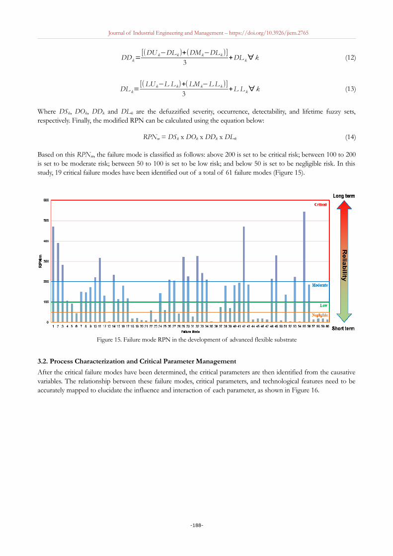
Based on this RPNm, the failure mode is classified as follows: above 200 is set to be critical risk; between 100 to 200is set to be moderate risk; between 50 to 100 is set to be low risk; and below 50 is set to be negligible risk. In thisstudy, 19 critical failure modes have been identified out of a total of 61 failure modes (Figure 15).
Figure 15. Failure mode RPN in the development of advanced flexible substrate
3.2. Process Characterization and Critical Parameter Management
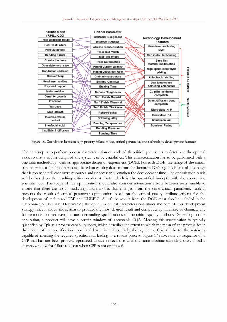
After the critical failure modes have been determined, the critical parameters are then identified from the causativevariables. The relationship between these failure modes, critical parameters, and technological features need to beaccurately mapped to elucidate the influence and interaction of each parameter, as shown in Figure 16.
-188-
Journal of Industrial Engineering and Management – https://doi.org/10.3926/jiem.2765
Figure 16. Correlation between high priority failure mode, critical parameter, and technology development features
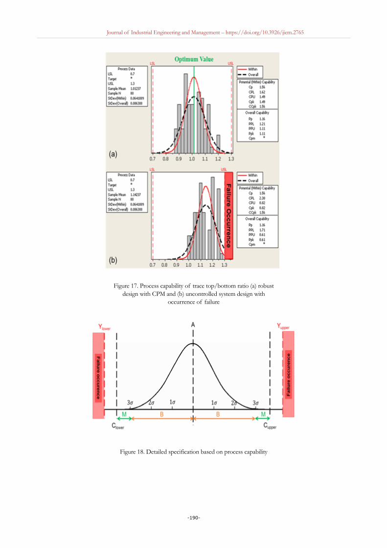
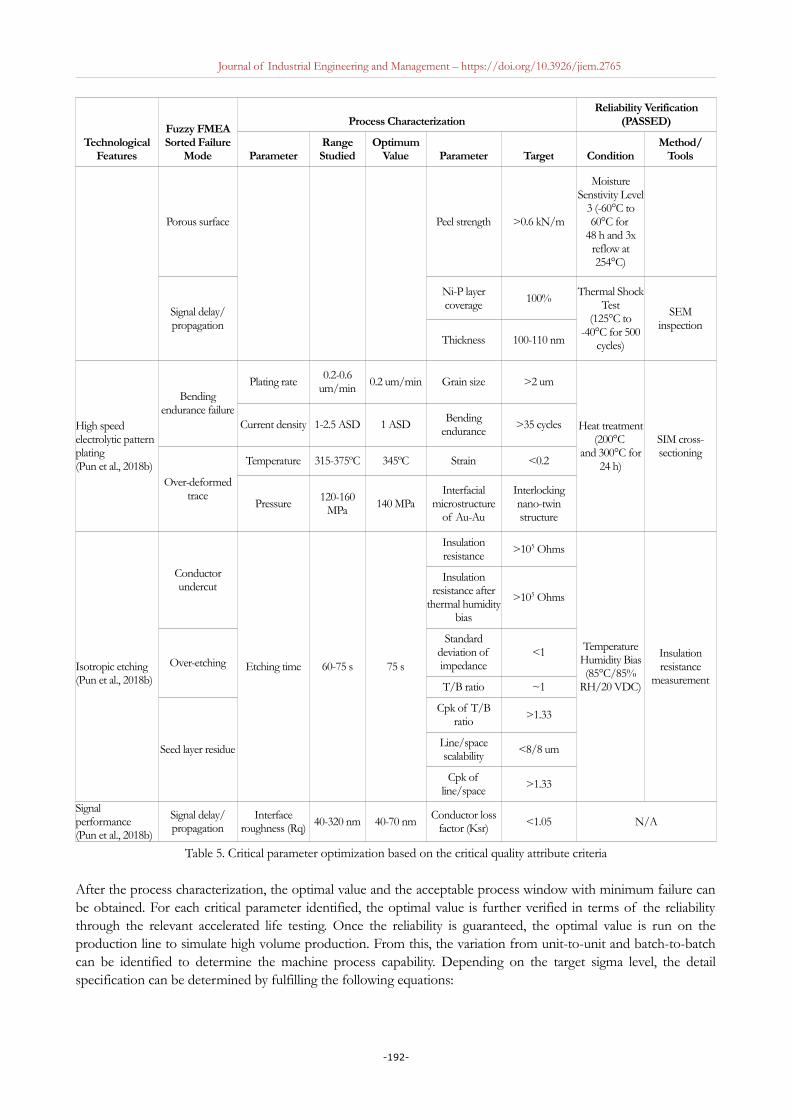
The next step is to perform process characterization on each of the critical parameters to determine the optimalvalue so that a robust design of the system can be established. This characterization has to be performed with ascientific methodology with an appropriate design of experiment (DOE). For each DOE, the range of the criticalparameter has to be first determined based on existing data or from the literature. Defining this is crucial, as a rangethat is too wide will cost more resources and unnecessarily lengthen the development time. The optimization resultwill be based on the resulting critical quality attribute, which is also quantified in-depth with the appropriatescientific tool. The scope of the optimization should also consider interaction effects between each variable toensure that there are no contradicting failure modes that emerged from the same critical parameter. Table 5presents the result of critical parameter optimization based on the critical quality attribute criteria for thedevelopment of reel-to-reel FAP and ENEPIG. All of the results from the DOE must also be included in theinterconnected database. Determining the optimum critical parameters constitutes the core of this developmentstrategy since it allows the system to produce the most desired result and consequently minimize or eliminate anyfailure mode to meet even the most demanding specifications of the critical quality attribute. Depending on theapplication, a product will have a certain window of acceptable CQA. Meeting this specification is typicallyquantified by Cpk as a process capability index, which describes the extent to which the mean of the process lies inthe middle of the specification upper and lower limit. Essentially, the higher the Cpk, the better the system iscapable of meeting the required specification, leading to a robust process. Figure 17 shows the consequence of aCPP that has not been properly optimized. It can be seen that with the same machine capability, there is still achance/window for failure to occur when CPP is not optimized.
-189-
Journal of Industrial Engineering and Management – https://doi.org/10.3926/jiem.2765
Figure 17. Process capability of trace top/bottom ratio (a) robustdesign with CPM and (b) uncontrolled system design with
occurrence of failure
Figure 18. Detailed specification based on process capability
-190-
Journal of Industrial Engineering and Management – https://doi.org/10.3926/jiem.2765
TechnologicalFeatures
Fuzzy FMEASorted Failure
Mode
Process CharacterizationReliability Verification
(PASSED)
ParameterRangeStudied
OptimumValue Parameter Target Condition
Method/Tools
Metallurgy diffusion bond compatible(Pun, Dhaka, Cheung & Chan, 2017a)
Interfacial void Temperature 180-340°C 320°C
Shear strength >50 MPaTemperature
HumidityStorage
(60°C/60%RH for 1000 h)
FIB cross-section
Insufficientdiffusion
Pressure 55-175 Mpa 155 Mpa
Insufficient/skip contact
Time 1-11 s 10 s
Exposed copper Ni Thickness 1-3 um 3.0 umTrace peeled off(peel test failure
mode)100%
Metal residue Pd Thickness 0.05-0.4 um 0.4 umBonding
misalignment<2 um
ThermalShock Test(125°C to-40°C for
1000 cycles)
Electrical testDendrite growth Au Thickness 0.04-0.07um
0.04 um
Void formation Fully shrunk
OxidationSurface
roughness (Ra)90-150 nm <100 nm
Cu pillar micro bump(C2) compatible(Pun, Islam, Cheung & Chan, 2017b)
IMCs growthNi Thickness 1-1.3 um 1 um
Overall IMCsthickness after
isothermal aging<4 um
Thermalaging 150°Cfor 1000 h
SEM/EDX& cross-
sectioning
Exposed copper
Metal residue Pd Thickness 0.05-0.4 um 0.05-0.2 umCritical IMCs
formed(Pd,Cu,Au)Sn4
(Cu,Ni)6Sn5
Dendrite growth
Au Thickness 0.04-0.2 um 0.04-0.07 um
Die peel failureinterface
Within solderside
OxidationGrowth rateconstant of
IMCs<2x10-14 cm2/s
Low temperature solder compatible(Sn-Bi-Ag)(Pun et al., 2018a)
IMCs growth Ni Thickness 1-4 um 1-1.5 um Shear strength >1000 gf
Extendedreflow at175°C for120 mins
SEM/EDX& cross-
sectioning
Exposed copper Pd Thickness 0.04-0.7 0.15-0.2 umFailure mode
100% solder oninterface
Metal residue
Au Thickness0.03-0.05
um 0.04 umDendrite growth
Critical IMCsformed
(Ni,Cu)3Sn4
Oxidation Ni consumption 0.009 um/minreflow
Base film modification and nano-level chemical bonding(Pun, Ali, Kohtoku, Cheung, Chan & Wong, 2018b)
Trace adhesionfailure
Modifierconcentration(on polyimide)
15-40 mL/L 25 mL/L
PAA layerthickness
<5 nm
TemperatureHumidityStorage
(85°/85% RH)
TEMinspection
Peel test failure
Carboxylbonding >3%
LowTemperature
Storage (-40°C for 500
h)XPS analysis
Amide bonding >6%
HightTemperature
Storage (150°Cfor 500h)
Peel test
-191-
Journal of Industrial Engineering and Management – https://doi.org/10.3926/jiem.2765
TechnologicalFeatures
Fuzzy FMEASorted Failure
Mode
Process CharacterizationReliability Verification
(PASSED)
ParameterRangeStudied
OptimumValue Parameter Target Condition
Method/Tools
MoistureSenstivity Level
3 (-60°C to60°C for
48 h and 3xreflow at254°C)
Porous surface Peel strength >0.6 kN/m
Signal delay/propagation
Ni-P layercoverage
100%Thermal Shock
Test(125°C to
-40°C for 500cycles)
SEMinspection
Thickness 100-110 nm
High speed electrolytic pattern plating(Pun et al., 2018b)
Bendingendurance failure
Plating rate0.2-0.6
um/min0.2 um/min Grain size >2 um
Heat treatment(200°C
and 300°C for24 h)
SIM cross-sectioning
Current density 1-2.5 ASD 1 ASD Bendingendurance
>35 cycles
Over-deformedtrace
Temperature 315-375ºC 345ºC Strain <0.2
Pressure120-160
MPa 140 MPaInterfacial
microstructureof Au-Au
Interlockingnano-twinstructure
Isotropic etching(Pun et al., 2018b)
Conductorundercut
Etching time 60-75 s 75 s
Insulationresistance
>105 Ohms
TemperatureHumidity Bias(85°C/85%
RH/20 VDC)
Insulationresistance
measurement
Insulationresistance after
thermal humiditybias
>105 Ohms
Over-etching
Standarddeviation ofimpedance
<1
T/B ratio ~1
Seed layer residue
Cpk of T/Bratio
>1.33
Line/spacescalability
<8/8 um
Cpk ofline/space
>1.33
Signal performance(Pun et al., 2018b)
Signal delay/propagation
Interfaceroughness (Rq) 40-320 nm 40-70 nm
Conductor lossfactor (Ksr) <1.05 N/A
Table 5. Critical parameter optimization based on the critical quality attribute criteria
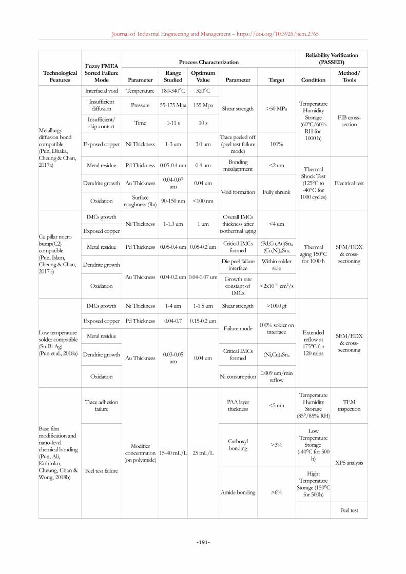
After the process characterization, the optimal value and the acceptable process window with minimum failure canbe obtained. For each critical parameter identified, the optimal value is further verified in terms of the reliabilitythrough the relevant accelerated life testing. Once the reliability is guaranteed, the optimal value is run on theproduction line to simulate high volume production. From this, the variation from unit-to-unit and batch-to-batchcan be identified to determine the machine process capability. Depending on the target sigma level, the detailspecification can be determined by fulfilling the following equations:
-192-
Journal of Industrial Engineering and Management – https://doi.org/10.3926/jiem.2765
Cupper = (A+B) + M (15)
Clower = (A-B) - M (16)
│Cupper – Yupper │≥ σ, Clowerr – Ylower ≥ σ (17)
where A is the optimal value from process characterization; Yupper and Ylower are the upper and lower limit before theoccurrence of failure, respectively; B is half of the target sigma level; Cupper and Clower are the lower and upperspecification, respectively; and M is the margin allowed for the specification as shown in Figure 18. Allowing thismargin is crucial so that room for error exists, which means that even though the process is outside of the sigmalevel standard, failure will still not occur. Obviously, the margin should be adjusted depending on the processcapability, targeted sigma level, and yield requirement.
Finally, the robust system has to be followed up by appropriate operational management practices so that theoptimum design can be carried out consistently throughout production. Critical parameter management is oneexcellent practice to assure that system robustness is maintained through detail specification, properdocumentation, and in line quality control (QC) (Clausing, Frey & Systems Engineering, 2010). With amanufacturing and production implementation plan for the critical parameters, quality evaluation, and changes inthe control plan, the value created through robust design can be delivered to the customer.
4. ConclusionEnabling robust technology transfer with minimum time-to-market constitutes the key to enhance businesscompetitiveness in high tech enterprises. With increasing complexity and diversification of products to meet futuremarket demands, a higher risk of failure is inevitable at the NPD stage. Field failure is particularly detrimental tomanufacturers, as failure occurs on the customer’s premise. This paper established a unique methodology ofprioritizing critical failure mode by embedding the product long term reliability into consideration usingfuzzy-based FMEA. The methodology is implemented on the development of advanced flexible substrate in theflexible electronics industry. It has been demonstrated that the methodology is capable of capturing the criticalfailure mode and consequently can be prevented through process characterization on the critical parameters. Finally,the reliability is also verified following the industry standard to ensure desirable and consistent performancethroughout product lifetime. Therefore, a balanced ecosystem of innovation can be realized by ensuring that thevalue created through new product development is thoroughly captured by commercialization in a timely manner.
Acknowledgement
The authors would like to acknowledge the support provided by the Compass Technology Co., Ltd.
Declaration of Conflicting InterestsThe authors declared no potential conflicts of interest with respect to the research, authorship, and/or publicationof this article.
Funding
The authors received no financial support for the research, authorship, and/or publication of this article.
ReferencesAoki, S. (2017). Devices, Materials, and Packaging Technologies for Hyperconnected Cloud. FUJITSU Sci Tech J,
53(2), 3-8.
Banduka, N, Tadić, D., Mačužić, I., & Crnjac, M. (2018). Extended process failure mode and effect analysis (PFMEA) for the automotive industry: The FSQC-PFMEA. Advances in Production Engineering & Management, 13(2),206-215. https://doi.org/10.14743/apem2018.2.285
-193-
Journal of Industrial Engineering and Management – https://doi.org/10.3926/jiem.2765
Baynal, K., Sari, T., & Akpinar, B. (2018). Risk management in automotive manufacturing process based on FMEA and grey relational analysis: A case study. Advances in Production Engineering & Management, 3(1), 69-80. https://doi.org/10.14743/apem2018.1.274
Belu, N., Rachieru, N., Militaru, E., & Anghel, D. (2012). Application of FMEA method in product development stage. Academic Journal of Manufacturing Engineering, 10(3), 12-19.
Bhuiyan, N. (2011). A Framework for successful new product development. Journal of Industrial Engineering and Management, 4(4), 746-770. https://doi.org/10.3926/jiem.334
Clausing, D., Frey, D., & Systems Engineering (2010) Massachusetts Institute of Technology: MIT Open Course Ware. Creative Commons BY-NC-SA. http://ocw.mit.edu
Crawford, C. (1987). New product management (2nd ed.). Illinois: Richard D. Irwin.
Doğan, O., & Cebeci U. (2016). A methodology for new product development by using QFD, FMEA and its application in metal plating industry. In 16th Production Research Symposium. At Istanbul, Turkey.
Kirkire, M.S., Rane, S.B., & Jadhav, J.R. (2015). Risk management in medical product development process using traditional FMEA and fuzzy linguistic approach: a case study. Journal of Industrial Engineering International, 11(4), 595-611. https://doi.org/10.1007/s40092-015-0113-y
Lau, J.H. (2015). 3D IC Integration and Packaging. McGraw Hill Professional.
Lee, T., Bieler, T.R., Kim, C., & Ma, H. (2015). Fundamentals of Lead-Free Solder Interconnect Technology From Microstructures to Reliability. Boston, MA: Springer US.
Lin, Q.L., Liu, L., Liu, H.C., & Wang, D.J. (2013). Integrating hierarchical balanced scorecard with fuzzy linguistic for evaluating operating room performance in hospitals. Expert Systems with Applications, 40(6), 1917-1924. https://doi.org/10.1016/j.eswa.2012.10.007
Mosley, T. (1994). Winning at new products: Accelerating the process from idea to launch (2nd ed.) by Robert G. Cooper. Reading, MA: Addison-Wesley Publishing Company, 1993. 358. Journal of Product Innovation Management, 11(4), 369-370. https://doi.org/10.1016/0737-6782(94)90105-8
Natarajan, M., Senthil, V., Devadasan, S.R., Mohan, N.V. & Sivaram, N.M. (2013). Quality and reliability in new product development. Journal of Manufacturing Technology Management, 24 (8), 1143-1162. https://doi.org/10.1108/JMTM-03-2011-0022
Nawrocki, W. (2010). Physical limits for scaling of integrated circuits. Journal of Physics: Conference Series, 248(1), 012059. https://doi.org/10.1088/1742-6596/248/1/012059
Nunes, M.L., Pereira, A., & Alves, A. (2017). Smart products development approaches for Industry 4.0. Procedia Manufacturing, 13, 1215-1222. https://doi.org/10.1016/j.promfg.2017.09.035
Pangracious, V., Marrakchi, Z., & Mehrez, H. (2015) Three-Dimensional Design Methodologies for Tree-based FPGA Architecture (13-41). Springer. https://doi.org/10.1007/978-3-319-19174-4
Pun, K.P., Dhaka, N.S., Cheung, C., & Chan, A.H. (2017a). Effect of ENEPIG metallization for solid-state gold-gold diffusion bonds. Microelectronics Reliability, 78, 339-348. https://doi.org/10.1016/j.microrel.2017.09.019
Pun, K.P., Islam, M.N., Cheung, C.W., & Chan, A.H. (2017b). Solid-state growth kinetics of intermetallic compounds in Cu pillar solder flip chip with ENEPIG surface finish under isothermal aging. Journal of Materials Science: Materials in Electronics, 28(17), 12617-12629. https://doi.org/10.1007/s10854-017-7086-0
Pun, K.P., Islam, M.N., Rotanson, J., Cheung, C., & Chan, A.H. (2018a). Enhancement of Sn-Bi-Ag Solder Joints with ENEPIG Surface Finish for Low-Temperature Interconnection. Journal of Electronic Materials, 47(9), 5191-5202. https://doi.org/10.1007/s11664-018-6385-4
-194-

Journal of Industrial Engineering and Management – https://doi.org/10.3926/jiem.2765
Pun, K.P., Ali, L., Kohtoku, M., Cheung, C., Chan, A.H., & Wong, C.P. (2018b). Latest advancement of fully additive process for 8 µm ultra-fine pitch chip-on-film (COF) by nano-size Ni–P metallization. Journal of Materials Science: Materials in Electronics, 29(8), 6937-6949. https://doi.org/10.1007/s10854-018-8680-5
Rajan R. (2016). Advancing Technological Innovation to Enable IoT’s Long Tail. Global Foundries. Available at: http://www.semiconwest.org/sites/semiconwest.org/files/data15/docs/Rajeev%20Rajan_GF.pdf
Schimmoeller, L.J. (2010). Success Factors of New Product Development Processes. Advances in Production Engineering & Management, 5(1), 25-32.
Synaptics (2014). White Paper: Latest Advances in Touch and Display Integration for Smartphones and Tablets. Synaptics Incorporated. https://www.synaptics.com/sites/default/files/touch-display-integration-smartphones-tablets.pdf
Würtenberger, J., Kloberdanz, H., Lotz, J., & Von Ahsen, A. (2014). Application of the fmea during the product development process – dependencies between level of information and quality of result. In DS 77: Proceedings of the DESIGN, 13th International Design Conference (417-426). Dubrovnik, Croatia.
Zahra, S.A. (1996). Technology strategy and financial performance: Examining the moderating role of the firms competitive environment. Journal of Business Venturing, 11(3), 189-219. https://doi.org/10.1016/0883-9026(96)00001-8
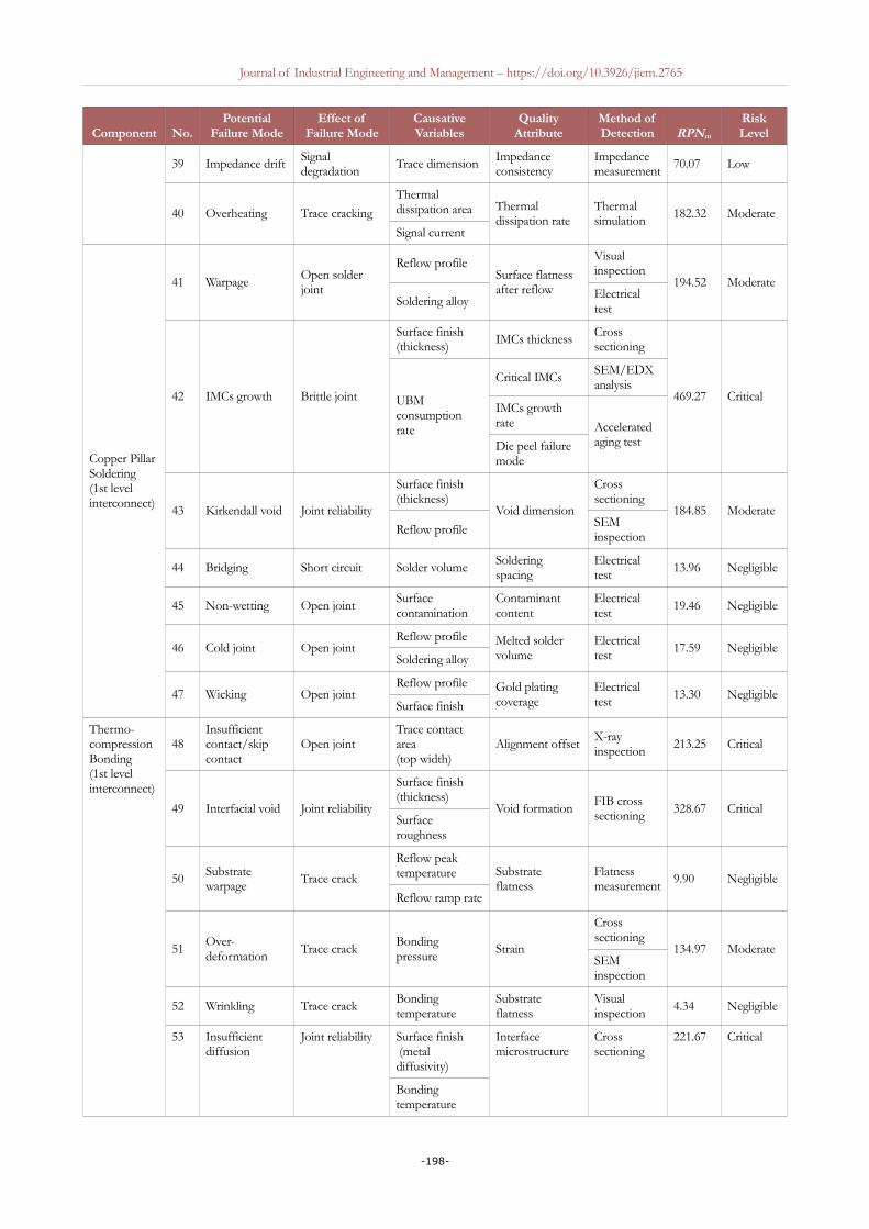
Appendix
Appendix A. List of failure modes
Component No.Potential
Failure ModeEffect of
Failure ModeCausativeVariables
QualityAttribute
Method ofDetection RPNm
RiskLevel
Base Film
1Trace adhesion failure Trace peeled off
Interfacial roughness
Bonding molecule composition
Surface profilometer
470.10 CriticalInterface bonding mechanism Anchoring layer
thickness
XPS analysis on bond content
Trace geometry (bottom width)
Cross sectional analysis
2 Peel test failure Trace peeled offAlkaline concentration
Peel strengthPeel strengthtest
390.10 Critical
3 Porous surface Skip pattern build up
Alkaline concentration
Modification layer coverage
SEM inspection
282.53 Critical
4 Entrapped contamination
Skip pattern build up
Chemical impurity level Contaminant
contentSEM/EDX analysis
106.35 Moderate
Handling
5 Scratch Open trace
Roller alignment
Scratch density
Visual inspection
91.46 Low
Particle deposition
Handling
Electrical simulation
6 Crack/separation
Open trace Reel tension Crack/separation density
Visual inspection
44.26 Negligible
7Skip/uneven plating
Skip pattern build up
Chemical concentration
Exposed PI region
Visual inspection
149.71 Moderate
8 Warpage Open trace Heat treatment profile
Surface flatness after reflow
Flatness measurement
146.95 Moderate
-195-
Journal of Industrial Engineering and Management – https://doi.org/10.3926/jiem.2765
Component No.Potential
Failure ModeEffect of
Failure ModeCausativeVariables
QualityAttribute
Method ofDetection RPNm
RiskLevel
CTE mismatch
9Non uniform surface morphology
Skip pattern build up
Incoming material defect
Surface defect density
SEM inspection
173.37 ModerateIncompatibility for high speed application
Cu Metallization
10Bending endurance failure
Trace crack
Current density Bending cycle Mandrel test
220.5 CriticalDeposition rate
Bending cycle (annealed)
SEM inspection
Grain microstructure
FIB cross sectioning
11
Signal delay/propagation Conductive loss
Incompatibility for high speed application
Surface roughness (skin depth)
Loss factor
Surface profilometer
316.60 CriticalSurface finish (material and thickness)
Electrical simulation
Trace undercut
12Trace overheating
Trace crack
Operating current Thermal
dissipation rateThermal simulation
130.34 ModerateTrace surface area
13
Surface abnormities Pits/Pinhole/Nodules
Open/short circuit
Current density
Surface defect density
SEM inspection
5.09 NegligibleDeposition rate
Chemical bath impurity
14Over-deformed trace
Intermittent connection
Plastic deformation characteristic
Strain
Cross sectionanalysis
233.30 CriticalSEM inspection
15 Via micro-void Signal integrityDeposition rate Void density Cross section
analysis112.50 Moderate
Residue Void size
16Non-Fully filled via
Signal integrity
Sidewall residue
Via volumeCross sectionanalysis
179.82 ModeratePolyimide melting
17 Uneven plating thickness
Not bondable surface
Residue deposit Surface flatnessSurface profilometer
116.58 ModerateSkip seed layer plating
18 Broken via sidewall
Open circuit Metallization integrity
Sidewall defect Electrical test
19.40 Negligible
19Bridging (bleeding)
Short circuit Resist adhesionInsulation resistance
Electrical test
21.60 Negligible
Photolithography
20 Resist bubbles Open/short circuit
Coater air entrapment
Resist surface defect
Visual inspection
11.37 Negligible
Lamination temperature
Lamination pressure
-196-
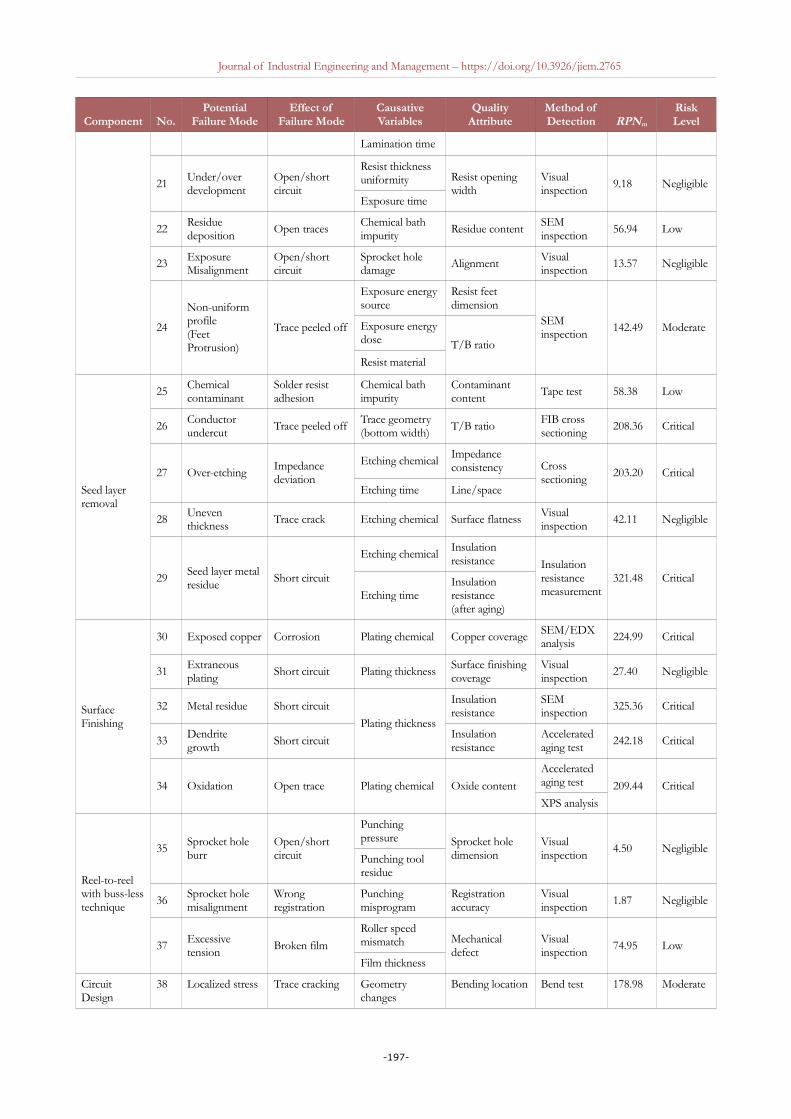
Journal of Industrial Engineering and Management – https://doi.org/10.3926/jiem.2765
Component No.Potential
Failure ModeEffect of
Failure ModeCausativeVariables
QualityAttribute
Method ofDetection RPNm
RiskLevel
Lamination time
21Under/over development
Open/short circuit
Resist thickness uniformity Resist opening
widthVisual inspection
9.18 Negligible
Exposure time
22Residue deposition
Open tracesChemical bath impurity
Residue contentSEM inspection
56.94 Low
23 Exposure Misalignment
Open/short circuit
Sprocket hole damage
Alignment Visual inspection
13.57 Negligible
24
Non-uniform profile (Feet Protrusion)
Trace peeled off
Exposure energysource
Resist feet dimension
SEM inspection
142.49 ModerateExposure energydose T/B ratio
Resist material
Seed layer removal
25Chemical contaminant
Solder resist adhesion
Chemical bath impurity
Contaminant content
Tape test 58.38 Low
26 Conductor undercut
Trace peeled off Trace geometry(bottom width)
T/B ratio FIB cross sectioning
208.36 Critical
27 Over-etchingImpedance deviation
Etching chemicalImpedance consistency Cross
sectioning203.20 Critical
Etching time Line/space
28 Uneven thickness
Trace crack Etching chemical Surface flatness Visual inspection
42.11 Negligible
29Seed layer metal residue
Short circuit
Etching chemicalInsulation resistance Insulation
resistance measurement
321.48 Critical
Etching timeInsulation resistance(after aging)
Surface Finishing
30 Exposed copper Corrosion Plating chemical Copper coverage SEM/EDX analysis
224.99 Critical
31Extraneous plating
Short circuit Plating thicknessSurface finishing coverage
Visual inspection
27.40 Negligible
32 Metal residue Short circuit
Plating thickness
Insulation resistance
SEM inspection
325.36 Critical
33Dendrite growth
Short circuitInsulation resistance
Accelerated aging test
242.18 Critical
34 Oxidation Open trace Plating chemical Oxide content
Accelerated aging test 209.44 Critical
XPS analysis
Reel-to-reel with buss-lesstechnique
35Sprocket hole burr
Open/short circuit
Punching pressure Sprocket hole
dimensionVisual inspection
4.50 NegligiblePunching tool residue
36Sprocket hole misalignment
Wrong registration
Punching misprogram
Registration accuracy
Visual inspection
1.87 Negligible
37Excessive tension
Broken film
Roller speed mismatch Mechanical
defectVisual inspection
74.95 Low
Film thickness
Circuit Design
38 Localized stress Trace cracking Geometry changes
Bending location Bend test 178.98 Moderate
-197-
Journal of Industrial Engineering and Management – https://doi.org/10.3926/jiem.2765
Component No.Potential
Failure ModeEffect of
Failure ModeCausativeVariables
QualityAttribute
Method ofDetection RPNm
RiskLevel
39 Impedance drift Signal degradation
Trace dimension Impedance consistency
Impedance measurement
70.07 Low
40 Overheating Trace cracking
Thermal dissipation area Thermal
dissipation rateThermal simulation
182.32 Moderate
Signal current
Copper Pillar Soldering (1st level interconnect)
41 WarpageOpen solder joint
Reflow profileSurface flatness after reflow
Visual inspection
194.52 Moderate
Soldering alloyElectrical test
42 IMCs growth Brittle joint
Surface finish (thickness)
IMCs thickness Cross sectioning
469.27 CriticalUBM consumption rate
Critical IMCsSEM/EDX analysis
IMCs growth rate Accelerated
aging testDie peel failure mode
43 Kirkendall void Joint reliability
Surface finish (thickness)
Void dimension
Cross sectioning
184.85 Moderate
Reflow profileSEM inspection
44 Bridging Short circuit Solder volume Soldering spacing
Electrical test
13.96 Negligible
45 Non-wetting Open jointSurface contamination
Contaminant content
Electrical test
19.46 Negligible
46 Cold joint Open jointReflow profile Melted solder
volumeElectrical test
17.59 NegligibleSoldering alloy
47 Wicking Open jointReflow profile Gold plating
coverageElectrical test
13.30 NegligibleSurface finish
Thermo-compression Bonding (1st level interconnect)
48Insufficient contact/skip contact
Open jointTrace contact area (top width)
Alignment offsetX-ray inspection
213.25 Critical
49 Interfacial void Joint reliability
Surface finish (thickness)
Void formationFIB cross sectioning 328.67 Critical
Surface roughness
50 Substrate warpage
Trace crack
Reflow peak temperature Substrate
flatnessFlatness measurement
9.90 Negligible
Reflow ramp rate
51Over-deformation
Trace crackBonding pressure
Strain
Cross sectioning
134.97 ModerateSEM inspection
52 Wrinkling Trace crackBonding temperature
Substrate flatness
Visual inspection
4.34 Negligible
53 Insufficient diffusion
Joint reliability Surface finish (metal diffusivity)
Interface microstructure
Cross sectioning
221.67 Critical
Bonding temperature
-198-
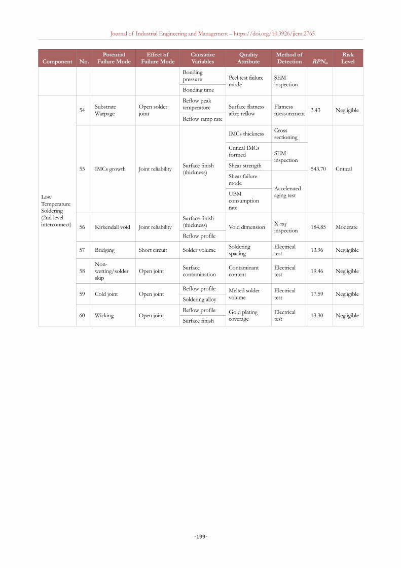
Journal of Industrial Engineering and Management – https://doi.org/10.3926/jiem.2765
Component No.Potential
Failure ModeEffect of
Failure ModeCausativeVariables
QualityAttribute
Method ofDetection RPNm
RiskLevel
Bonding pressure Peel test failure
modeSEM inspection
Bonding time
Low Temperature Soldering (2nd level interconnect)
54Substrate Warpage
Open solder joint
Reflow peak temperature Surface flatness
after reflowFlatness measurement
3.43 Negligible
Reflow ramp rate
55 IMCs growth Joint reliability Surface finish (thickness)
IMCs thickness Cross sectioning
543.70 Critical
Critical IMCs formed SEM
inspectionShear strength
Shear failure mode
Accelerated aging testUBM
consumption rate
56 Kirkendall void Joint reliability
Surface finish (thickness) Void dimension X-ray
inspection184.85 Moderate
Reflow profile
57 Bridging Short circuit Solder volume Soldering spacing
Electrical test
13.96 Negligible
58Non-wetting/solder skip
Open jointSurface contamination
Contaminant content
Electrical test 19.46 Negligible
59 Cold joint Open jointReflow profile Melted solder
volumeElectrical test 17.59 Negligible
Soldering alloy
60 Wicking Open jointReflow profile Gold plating
coverageElectrical test 13.30 Negligible
Surface finish
-199-
Journal of Industrial Engineering and Management – https://doi.org/10.3926/jiem.2765
Appendix B. Evaluation of severity, occurrence, detection, and lifetime by experts using fuzzy linguistic terms
Journal of Industrial Engineering and Management, 2019 (www.jiem.org)
Article’s contents are provided on an Attribution-Non Commercial 4.0 Creative commons International License. Readers areallowed to copy, distribute and communicate article’s contents, provided the author’s and Journal of Industrial Engineering andManagement’s names are included. It must not be used for commercial purposes. To see the complete license contents, please
visit https://creativecommons.org/licenses/by-nc/4.0/.
-200-


![Using Fuzzy FMEA Approach to Improve Decision-Making ...ijiepr.iust.ac.ir/article-1-835-en.pdf[10] considered FMEA in Amhara Pipe Factory P.L.C., Bahir Dar, and Ethiopia. Three key](https://img.pdfslide.us/doc/110x75/5e9f9a8c3b06ea576c5b946b/using-fuzzy-fmea-approach-to-improve-decision-making-10-considered-fmea-in.jpg)