Embed Size (px)
Citation preview

4
Application of Electron Beam Treatment in Polycrystalline Silicon Films
Manufacture for Solar Cell
L. Fu College of Materials Science, Northwestern Polytechnical University, Xian,
State Key Laboratory of Solidification Processing P. R. China
1. Introduction
Solar cell attracts more and more attentions recently since it transfers and storages energy directly from the sun light without consuming natural resources on the earth and polluting environment. In 2002, the solar industry delivered more than 500 MW per year of photovoltaic generators. More than 85% of the current production involved crystalline silicon technologies. These technologies still have a high cost reduction potential, but this will be limited by the silicon feedstock (Diehl et al., 2005; Lee et al., 2004). On the other hand the so-called second generation thin film solar cells based on a-Si, μc-Si, Cu(In,Ga)(Se,S)2, rare earth or CdTe have been explored(Shah et al.,2005; Li et al.,2004). Crystalline silicon on glass (CSG) solar cell technology was recently developed by depositing silicon film on a glass substrate with an interlayer. It can addresses the difficulty that silicon wafer-based technology has in reaching the very low costs required for large-scale photovoltaic applications as well as the perceived fundamental difficulties with other thin-film technologies (M. A. Green et al., 2004). This technology combines the advantages of standard silicon wafer-based technology, namely ruggedness, durability, good electronic properties and environmental soundness with the advantages of thin-films, specifically low material use, large monolithic construction and a desirable glass substrate configuration. This Chapter will descript research about the polycrystalline silicon thin film absorber based on CSG technology with high efficiency. Line shaped electron beam recrystallized polycrystalline silicon films of a 20μm thickness deposited on the low cost borosilicate glass-substrate, which are the base for a solar cell absorber with high efficiency and throughput. It is known that the morphology of polycrystalline silicon film and grain boundaries have strong impact on the photoelectric transformation efficiency in the later cell system. Thus, this study concentrates on the influence of recrystallization on the silicon-contact interface and the surface morphology.
2. Experiment methods
Fig. 1 shows the schematic illustration of the silicon solar cell used in this work. The substrate of polycrystalline silicon thin film is Borosilicate glass, which is 10×10×0.07cm3 in size. A pure tungsten layer of 1.2µm was sputtered on the glass substrate at DC of 500W in
www.intechopen.com

Solar Cells – Thin-Film Technologies
78
an argon atmosphere, which has almost the same thermal expansion coefficient of 4.5×10⁻⁶K-
1 as that of the silicon film (Linke et al., 2004; Goesmann et al., 1995). This tungsten interlayer was used as a thermal and mechanical supporting layer for deposition of the silicon film. Nanocrystalline silicon films were then deposited on the tungsten interlayer by the plasma enhanced chemical vapour deposition process (PECVD) within SiHCl3 and H2 atmosphere. Details of the process were described in References (Rostalsky et al., 2001; Gromball et al., 2004, 2005). The power density used was 2.5W/cm2. The gap in the PECVD parallel plate reactor was 10mm and the substrate temperature was 550℃. The flow rate H2/SiHCl3 is 0.25 to reduce the hydrogen and chlorine content in the film. Boron trichloride (BCl3) was added in the gas for an in-situ p-doping. The process pressure was chosen to 350 Pa for the minimized stress. At the above conditions, the deposition rate up to 200nm/min was obtained. After a silicon film of 15-20μm thickness was deposited, a SiO2 layer of 400nm thickness was deposited on the top of the silicon from SiHCl3 and N2O within 5 min to prevent balling up.
Fig. 1. Structure of thin film silicon solar cell
Fig. 2. Schematic of the linear electron beam recrystallization system (Gromball et al., 2005)
www.intechopen.com
Application of Electron Beam Treatment in Polycrystalline Silicon Films Manufacture for Solar Cell
79
The P-doped polycrystalline silicon absorber of 10cm² was melted and recrystallized by a controlled line shaped electron beam (size in 1×100mm2) as described in Fig.2. The appearance of the sample after recrystallization was shown in Fig.3. The samples are preheated from the backside to 500°C within 2 min by halogen lamps. The electron beam energy density applies to the films is a function of the emission current density, the accelerating voltage and the scan speed. The scan speed is chosen to 8mm/s and the applied energy density changes between 0.34J/mm2 and 0.4J/mm2. To obtain the required grain size, the silicon should be melted and re-crystallized. Therefore, temperature in the electron beam radiation region should be was over the melting point of silicon of 1414°C. The surface morphology of the film, as well as distribution of WSi2 phase under different energy densities has been investigated by means of a LEO-32 Scanning Electron Microscopy.
Fig. 3. Appearance of polycrystalline silicon absorber after recrystallization
3. Results and discussion
3.1 Microstructure of the capping layer The applied recrystallization energy density strongly influences the surface morphology and
microstructure of the recrystallized silicon film. With the energy increasing, the capping
layer becomes smooth and continuous and less and small pinholes form in the silicon film.
Excess of recrystallization energy density leads to larger voids in the capping layer, more
WSi2/Si eutectic crystallites, a thinner tungsten layer and a thicker tungstendisilicide layer.
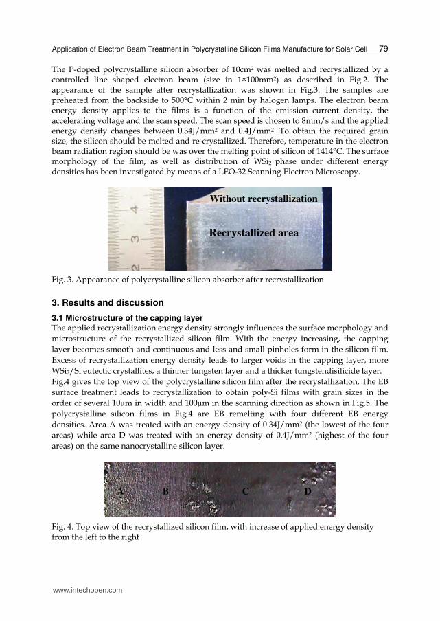
Fig.4 gives the top view of the polycrystalline silicon film after the recrystallization. The EB
surface treatment leads to recrystallization to obtain poly-Si films with grain sizes in the
order of several 10µm in width and 100µm in the scanning direction as shown in Fig.5. The
polycrystalline silicon films in Fig.4 are EB remelting with four different EB energy
densities. Area A was treated with an energy density of 0.34J/mm2 (the lowest of the four
areas) while area D was treated with an energy density of 0.4J/mm2 (highest of the four
areas) on the same nanocrystalline silicon layer.
A B C D
Fig. 4. Top view of the recrystallized silicon film, with increase of applied energy density from the left to the right
Without recrystallization
Recrystallized area
www.intechopen.com

Solar Cells – Thin-Film Technologies
80
Fig. 5. Grain microstructure of Ploy-Silicon absorber after recrystallization
(a) є=0.34J/mm2 ; (b) є=0.36J/mm2 ; (c) є=0.38J/mm2; (d) є=0.4J/mm2
Fig. 6. Surface morphology of the recrystallized silicon layer under different energy density є (Fu et al., 2007)
50µm
Scanning
direction
(a) (b)
(c) (d)
Pinhol
Voids
www.intechopen.com

Application of Electron Beam Treatment in Polycrystalline Silicon Films Manufacture for Solar Cell
81
Fig.6 and Fig.7 show the morphology and microstructure of the EB treated layers. The nanocrystalline silicon is zone melted and recrystallized (ZMR) completely under all the energy chosen in this experiment. It can be seen that after the EB surface treatment, micro-sized silicon grains were formed in all the samples treated under different electron beam energy density є. The outmost surface was silicon dioxides with some voids and pinholes (bright spots), as shown in Fig.6. Large areas with a rough surface were where the silicon dioxide capping layer (SiO2) existed. The voids (the dark area in Fig.6) in the silicon dioxide capping layer penetrated into the silicon layer with smooth edges. The bright areas were the bottom of the pinholes in which the WSi2 remained. Influences of the EB energy density on the morphology of deposited films are summarized in Table 1. The energy density influences the surface morphology of the film system strongly. The capping layer exhibited more voids when a lower EB energy density was used, as shown in Fig.6a. The SiO2 capping layer is rougher and appeared as discontinuous droplet morphology in this condition. In addition, large tungstendisilicide pinholes formed due to the lower fluidity and less reaction between the silicon melt and the tungsten interlayer. When the EB energy density was increased, the capping layer becomes smoother and the size of voids was reduced. The number and size of pinholes also became smaller. However, when excess EB energy was applied, the solidification process became unstable and the amount of pinholes increased again. The silicon dioxide capping layer became discontinuous in this case, as shown in Fig. 6d.
(a) є=0.34J/mm2 ; (b) є=0.4J/mm2
Fig. 7. Microstructure of the capping layer and silicon grain under different energy density є (Fu et al., 2007)
It was suggested that the voids are caused by the volume change of the capping layer and the silicon melt during the recrystallization process. Early work [6] suggested that the silicon dioxide in the capping layer could be considered as a fluid with a relatively high viscosity at the EB treatment temperature. For the same amount of silicon, the volume of the solid VS is about 1.1 times of that of the liquid VL. Therefore, during solidification process of the silicon melt, the volume increases will produce a curved melt surface. This will generates a tensile stress in the capping layer because of he interface enlargement between the viscous capping layer and the molten silicon. Once the critical strain of the capping layer is surpassed, voids will form in the capping layer. Due to the surface tension of the capping layer and its
(a) (b) Cappi
Pinhol
Silicon Silicon
Cappi
Pinhol
www.intechopen.com

Solar Cells – Thin-Film Technologies
82
adhesion to the silicon melt the capping layer also arches upwards and widens the voids. This effect is enhanced by thermal stress and outgassing during the solidification process [5]. As the size, area and viscosity of the SiO2 layer is affected by the EB energy density, the size and the number of the voids in the capping layer are dependant on the EB energy density as well.
Energy level SiO2 capping/ voids pinholes Wremaining/ WSi2 ratio
WSi2 /Si eutectic
Low (0.34J/mm2)
rough, droplet morphology
High density, biggest (>200µm)
21.7% fine
Middle (0.36-0.38J/mm2)
smooth, continuoussporadic, small size
(<50µm) 13.3% coarse
High (0.4J/mm2)
smooth, discontinuous
Low density, bigger(<100µm)
10.5% coarser and
widely spread
Table 1. Influence of the recrystallization energy on the surface morphology of the silicon film system
3.2 Formation of eutectic (WSi2/Si) This Chapter gives the details about the formation of Tungstendisilicide (WSi2). The film
system consists of a 20μm thick silicon layer on a 1.2μm thick tungsten film.
Tungstendisilicide (WSi2) is formed at the interface tungsten/silicon but also at the grain
boundaries of the silicon. Because of the fast melting and cooling of the silicon film, the
solidification process of the silicon film is a nonequilibrium solidification process.
It was claimed that tungstendisilicides were formed in their tetragonal (Hansen, 1958;
Döscher et al., 1994) by the solid/solid state reaction and the solid/liquid state reaction
between tungsten and silicon according to equation (1) and (2).
700 1390( ) ( ) 2( )2 C Cs s sSi W WSi (1)
1390( ) ( ) 2( )2 Cl s sSi W WSi (2)
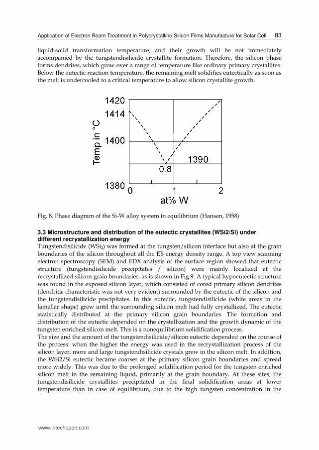
Formation of the eutectics can be explained using the phase diagram of the Si-W alloy system, as shown in Fig.8. The reactions should start at temperatures above 700°C. The eutectic crystallites (WSi2/Si) are precipitated from the silicon melt at a eutectic concentration of 0.8 at% W at the eutectic temperature 1390°C in thermal equilibrium. With the temperature increased to above the eutectic temperature (1390°C) for tungsten enriched silicon melt, the WSi2 layer mainly formed through a solid-liquid reaction and the thickness of the silicide layer increased rapidly. Because 100ms (the FWHM of the electron beam related to the scan speed) were sufficient to generate the tungstendisilicide layer. However, in this experiment, the solidification process of the nanocrystalline silicon was completed within 12.5 seconds for a sample of 10cm2 area. Therefore, the solidification process was completed in a nonequilibrium state and the liquid-solid transformation line will divert from equilibrium line shown in Fig.8. At the beginning of the silicon solidification, the formation of tungstendisilicide crystallites will be suppressed by the rapid freezing and followed by the formation of solid silicon. These crystallites start to form just below the
www.intechopen.com
Application of Electron Beam Treatment in Polycrystalline Silicon Films Manufacture for Solar Cell
83
liquid-solid transformation temperature, and their growth will be not immediately accompanied by the tungstendisilicide crystallite formation. Therefore, the silicon phase forms dendrites, which grow over a range of temperature like ordinary primary crystallites. Below the eutectic reaction temperature, the remaining melt solidifies eutectically as soon as the melt is undercooled to a critical temperature to allow silicon crystallite growth.
Fig. 8. Phase diagram of the Si-W alloy system in equilibrium (Hansen, 1958)
3.3 Microstructure and distribution of the eutectic crystallites (WSi2/Si) under different recrystallization energy Tungstendisilicide (WSi2) was formed at the tungsten/silicon interface but also at the grain
boundaries of the silicon throughout all the EB energy density range. A top view scanning
electron spectroscopy (SEM) and EDX analysis of the surface region showed that eutectic
structure (tungstendisilicide precipitates / silicon) were mainly localized at the
recrystallized silicon grain boundaries, as is shown in Fig.9. A typical hypoeutectic structure
was found in the exposed silicon layer, which consisted of cored primary silicon dendrites
(dendritic characteristic was not very evident) surrounded by the eutectic of the silicon and
the tungstendisilicide precipitates. In this eutectic, tungstendisilicide (white areas in the
lamellar shape) grew until the surrounding silicon melt had fully crystallized. The eutectic
statistically distributed at the primary silicon grain boundaries. The formation and
distribution of the eutectic depended on the crystallization and the growth dynamic of the
tungsten enriched silicon melt. This is a nonequilibrium solidification process.
The size and the amount of the tungstendisilicide/silicon eutectic depended on the course of the process: when the higher the energy was used in the recrystallization process of the silicon layer, more and large tungstendisilicide crystals grew in the silicon melt. In addition, the WSi2/Si eutectic became coarser at the primary silicon grain boundaries and spread more widely. This was due to the prolonged solidification period for the tungsten enriched silicon melt in the remaining liquid, primarily at the grain boundary. At these sites, the tungstendisilicide crystallites precipitated in the final solidification areas at lower temperature than in case of equilibrium, due to the high tungsten concentration in the
www.intechopen.com

Solar Cells – Thin-Film Technologies
84
(a) є=0.34J/mm2; (b) є=0.36J/mm2; (c) є=0.38J/mm2; (d) є=0.4J/mm2
Fig. 9. SEM results of the eutectic structure under different recrystallization energy density є (Fu et al., 2007)
(a) є=0.34J/mm2 ; (b) є=0.40J/mm2
Fig. 10. Cross section of typical silicon film system under different energy density є (Fu et al., 2007)
(a) (b)
(c) (d)
(a) (b)
WSi2
W
S
W
WSi2
S
www.intechopen.com
Application of Electron Beam Treatment in Polycrystalline Silicon Films Manufacture for Solar Cell
85
volume. For high EB energy density there was more time for the precipitation and growth of tungstendisilicide and thus more tungstendisilicide crystallites were precipitated at the silicon grain boundaries. The strong tendency of formation of tungstendisilicide at the primary grain boundaries would reduce the efficiency of the solar absorber. Thus a high energy density is not favorable for the recrystallization process. Fig.10 shows the cross section of a typical resolidified silicon film remelted with different EB energy densities. Tungstendisilicides (WSi2) were formed in the region between the tungsten layer and the silicon layer without relationship to the EB energy density range applied in this research. A thick tungstendisilicide of 2.0-2.86μm exhibited in this experiment. The higher the applied EB energy density, the thicker the tungstendisilicide layer between the tungsten and the silicon layer, the thinner the remaining tungsten layer will be.
0 100 200 300 400 500
1
10
100
1000
10000 O
Si
W
rela
tive in
tensity (
a.u
.)
distance (um)
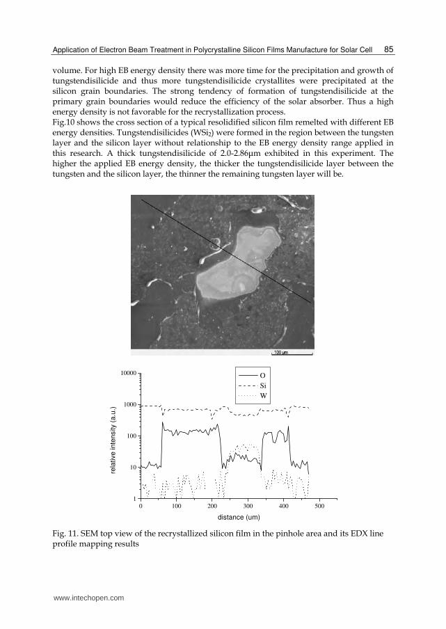
Fig. 11. SEM top view of the recrystallized silicon film in the pinhole area and its EDX line profile mapping results
www.intechopen.com

Solar Cells – Thin-Film Technologies
86
3.4 Impurities in the recrystallized silicon film The relatively high chlorine and hydrogen concentrations in the order of 0.5at% lead to
outgassing during the recrystallization in completely melting regimes. This effect makes the
capping layer arch upwards and widens the voids. Isolated pinholes in the silicon film can
be observed. A weak hydrogen chloride peak is detected by mass spectrometry in the base
gas atmosphere of the recrystallization chamber. Fig.11 shows an area surrounding a
pinhole taken with SEM and the relative element concentrations measured by energy
dispersive x-ray analysis (EDX) along the black line. There are no chlorine and hydrogen in
the area surrounding a pinhole in the recrystallized film.
4. Summary
This Chapter descried the influence of the applied EB energy density used for the
recrystallization process on the surface morphology of the ploy-silicon film system. At a low
EB energy density, the voids were formed in the capping layer and the SiO2 capping layer
exhibited a rougher and droplet morphology. With the increase of EB energy density, the
capping layer became smooth and the size of the voids decreased. The size and amount of
pinholes increased again if the EB energy density was too high. This also led to the
formation of larger voids in the capping layer as well as coarser and wider spreading of a
WSi2/Si eutectic crystallite at the grain boundaries.
This Chapter also gave the details about the formation of Tungstendisilicide (WSi2). The
tungstendisilicide precipitates/silicon eutectic structures were mainly localized in at the
tungsten/silicon interface but also at the grain boundaries of the silicon throughout all the
EB energy density range, as well as the relationship between energy density and
microstructure of WSi2/W areas. Tungstendisilicide forms in its tetragonal by the reaction of
tungsten with silicon. WSi2 improves the wetting and adhesion of the silicon melt but the
tungsten layer may degrade the electrical properties of the solar absorber. The formation
and distribution of the eutectic depended on the crystallization and the growth dynamic of
the tungsten enriched silicon melt. This is a nonequilibrium solidification process.
A tungstendisilicide layer was formed between the tungsten layer and the silicon layer for
all EB energy densities used. The higher the applied EB energy density, the thicker the
tungstendisilicide layer grows and the thinner the tungsten layer left. It is important to
perform the recrystallization process at a moderate energy density to suppress the formation
of both WSi2/Si eutectic and pinholes. In addition, there are no chlorine and hydrogen in the
area surrounding a pinhole after recrystallization because of outgassing during the
solidification.
5. Acknowledgements
The author would like to thank Prof. J. Müller and Dr. F. Gromball of Technische Universit.t
Hamburg-Harburg in Germany for providing experimental conditions and interesting
discussion, and also remember Prof. J. Müller with affection for his human and scientific
talents. This research was financially supported by the German Federal Ministry for the
Environment, Nature Conservation and Nuclear Safety under contract #0329571B in
collaboration with the Hahn Meitner Institute (HMI), Berlin-Adlershof, Department for
Solar Energy Research. The author was financially supported by China Scholarship Council
www.intechopen.com

Application of Electron Beam Treatment in Polycrystalline Silicon Films Manufacture for Solar Cell
87
(CSC) and the Research Fund of the State Key Laboratory of Solidification Processing
(NWPU), China (Grant No. 78-QP-2011).
6. References
Diehl W., Sittinger V. & Szyszka B. (2005). Thin film solar cell technology in Germany.
Surface and Coatings Technology, Vol.193, No. 1-3, (April 2005), pp.329-334, ISSN:
0257-8972
Döscher M., Pauli M. and Müller J. (1994). A study on WSi2 thin films, formed by the
reaction of tungsten with solid or liquid silicon by rapid thermal annealing. Thin
Solid Films, Vol.239, No. 2, (March 1994), pp.251-258, ISSN: 0040-6090
Dutartre D. (1989). Mechanics of the silica cap during zone melting of Si films. Journal of
Apply Physics, Vol.66, No. 3, (August 1989), pp.1388-1391, ISSN: 0021-8979
Fu L., Gromball F., Groth C., Ong K., Linke N. & Müller J. (2007). Influence of the energy
density on the structure and morphology of polycrystalline silicon films treated
with electron beam. Materials Science and Engineering B, Vol.136, No. 1, (January
2007), pp.87–91, ISSN: 0921-5107
Green M. A., Basore P. A., Chang N., Clugston D., Egan R., Evans R. Hogg D., Jarnason
S., Keevers M., Lasswell P., O’Sullivan J., Schubert U., Turner A., Wenham S. R.
& Young T. (2004). Crystalline silicon on glass (CSG) thin-film solar cell
modules. Solar Energy. Vol.77, No. 6, (December 2004) , pp.857-863, ISSN: 0038-
092X
Goesmann F. & Schmid-Fetzer R. (1995). Stability of W as electrical contact on 6H-SiC: phase
relations and interface reactions in the ternary system W-Si-C. Materials Science and
Engineering B, Vol. 34, No. 2-3, (November 1995), pp.224-231, ISSN: 0921-5107
Gromball F., Heemeier J., Linke N., Burchert M. & Müller J. (2004). High rate deposition and
in situ doping of silicon films for solar cells on glass. Solar Energy Materials & Solar
Cells, Vol.84, No. 1-4, (October 2004), pp.71-82, ISSN: 0927-0248
Gromball F., Ong K., Groth C., Fu L., Müller J., Strub E., Bohne W. & Röhrich J. (2005).
Impurities in electron beam recryatallised silicon absorbers on glass, Proceedings of
20th European Photovoltaic Solar Energy Conference and Exhibition, Barcelona, Span,
July, 2005.
Hansen M. (1958). Constitution of binary alloys, In: Metallurgy and Metallurgical Engineering
Series, Kurt Anderko, pp.100-1324, McGraw-Hill Book Company, ISBN-13: 978-
0931690181, ISBN-10: 0931690188, London
Lee G. H., Rhee C. K. & Lim K. S. (2006). A study on the fabrication of polycrystalline Si
wafer by direct casting for solar cell substrate. Solar Energy, Vol.80, No. 2, (February
2006), pp.220-225, ISSN: 0038-092X
Li B. J., Zhang C. H. & Yang T. (2005). Journal of Rare Earths. Vol.23, No. 2, (April 2005),
pp.228-230, ISSN: 1002-0721
Linke N., Gromball F., Heemeier J. & Mueller J. (2004). Tungsten silicide as supporting
layer for electron beam recryatallised silicon solar cells on glass, Proceedings of
19th European Photovoltaic Solar Energy Conference and Exhibition, Paris, France,
July, 2004.
www.intechopen.com

Solar Cells – Thin-Film Technologies
88
Rostalsky M. & Mueller J. (2001). High rate deposition and electron beam recrystallization of
silicon films for solar cells. Thin Solid Films, Vol.401, No. 1-2, (December 2001),
pp.84-87, ISSN: 0040-6090
Shah A. V., Schade H., Vanecek M., Meier J., Vallat-Sauvain E., Wyrsch N., Kroll U., Droz
C. & Bailat J. (2004). Thin-film silicon solar cell technology. Progress in
Photovoltaics: Research and Applications. Vol.12, No. 2-3, (March 2004), pp.113-142,
ISSN: 1099-159X
www.intechopen.com

Solar Cells - Thin-Film TechnologiesEdited by Prof. Leonid A. Kosyachenko
ISBN 978-953-307-570-9Hard cover, 456 pagesPublisher InTechPublished online 02, November, 2011Published in print edition November, 2011
InTech EuropeUniversity Campus STeP Ri Slavka Krautzeka 83/A 51000 Rijeka, Croatia Phone: +385 (51) 770 447 Fax: +385 (51) 686 166www.intechopen.com
InTech ChinaUnit 405, Office Block, Hotel Equatorial Shanghai No.65, Yan An Road (West), Shanghai, 200040, China
Phone: +86-21-62489820 Fax: +86-21-62489821
The first book of this four-volume edition is dedicated to one of the most promising areas of photovoltaics,which has already reached a large-scale production of the second-generation thin-film solar modules and hasresulted in building the powerful solar plants in several countries around the world. Thin-film technologiesusing direct-gap semiconductors such as CIGS and CdTe offer the lowest manufacturing costs and arebecoming more prevalent in the industry allowing to improve manufacturability of the production at significantlylarger scales than for wafer or ribbon Si modules. It is only a matter of time before thin films like CIGS andCdTe will replace wafer-based silicon solar cells as the dominant photovoltaic technology. Photoelectricefficiency of thin-film solar modules is still far from the theoretical limit. The scientific and technologicalproblems of increasing this key parameter of the solar cell are discussed in several chapters of this volume.
How to referenceIn order to correctly reference this scholarly work, feel free to copy and paste the following:
L. Fu (2011). Application of Electron Beam Treatment in Polycrystalline Silicon Films Manufacture for SolarCell, Solar Cells - Thin-Film Technologies, Prof. Leonid A. Kosyachenko (Ed.), ISBN: 978-953-307-570-9,InTech, Available from: http://www.intechopen.com/books/solar-cells-thin-film-technologies/application-of-electron-beam-treatment-in-polycrystalline-silicon-films-manufacture-for-solar-cell

© 2011 The Author(s). Licensee IntechOpen. This is an open access articledistributed under the terms of the Creative Commons Attribution 3.0License, which permits unrestricted use, distribution, and reproduction inany medium, provided the original work is properly cited.