Embed Size (px)
Citation preview

M9328MX1ADSUM/DRev 2October 29, 2002
User’s Manual
M9328MX1ADSApplication
Development System
User’s Manual
© Motorola, Inc., 2002
Important Notice to Users
While every effort has been made to ensure the accuracy of all information in this document, Motorola assumes no liability to any party for any loss or damage caused by errors or omissions or by statements of any kind in this document, its updates, supplements, or special editions, whether such errors are omissions or statements resulting from negligence, accident, or any other cause. Motorola further assumes no liability arising out of the application or use of any information, product, or system described herein: nor any liability for incidental or consequential damages arising from the use of this document. Motorola disclaims all warranties regarding the information contained herein, whether expressed, implied, or statutory, including implied warranties of merchantability or fitness for a particular purpose. Motorola makes no representation that the interconnection of products in the manner described herein will not infringe on existing or future patent rights, nor do the descriptions contained herein imply the granting or license to make, use or sell equipment constructed in accordance with this description.
Trademarks
This document includes these trademarks:
Motorola and the Motorola logo are registered trademarks of Motorola, Inc.
Windows is a registered trademark of Microsoft Corporation in the U.S. and other countries.
Intel is a registered trademark of Intel Corporation.
Motorola, Inc., is an Equal Opportunity / Affirmative Action Employer.
For an electronic copy of this book, visit Motorola’s web site at http://e-www.motorola.com/
© Motorola, Inc., 2002; All Rights Reserved
M9328MX1ADS Application Development System - Rev 2 User’s Manual
2 MOTOROLA
Table Of Contents
Section 1 General Information1.1 Description . . . . . . . . . . . . . . . . . . . . . . . . . . . . . . . . . . . . . . . . . . . . . . 3
1.2 Features . . . . . . . . . . . . . . . . . . . . . . . . . . . . . . . . . . . . . . . . . . . . . . . . . 3
1.3 System and User Requirements . . . . . . . . . . . . . . . . . . . . . . . . . . . . . . 5
1.4 MX1ADS Diagram . . . . . . . . . . . . . . . . . . . . . . . . . . . . . . . . . . . . . . . . 6
1.5 Specifications . . . . . . . . . . . . . . . . . . . . . . . . . . . . . . . . . . . . . . . . . . . . 8
Section 2 Configuration and Operation2.1 Introduction. . . . . . . . . . . . . . . . . . . . . . . . . . . . . . . . . . . . . . . . . . . . . . 9
2.2 Configuring Board Components . . . . . . . . . . . . . . . . . . . . . . . . . . . . . . 92.2.1 Peripheral Selection Switch (S1) . . . . . . . . . . . . . . . . . . . . . . . . . . 102.2.2 Mode Switch (S22) . . . . . . . . . . . . . . . . . . . . . . . . . . . . . . . . . . . . 11
2.3 Operation . . . . . . . . . . . . . . . . . . . . . . . . . . . . . . . . . . . . . . . . . . . . . . 132.3.1 Functional Block Diagram. . . . . . . . . . . . . . . . . . . . . . . . . . . . . . . 132.3.2 On Board Memory . . . . . . . . . . . . . . . . . . . . . . . . . . . . . . . . . . . . . 142.3.3 Memory Map . . . . . . . . . . . . . . . . . . . . . . . . . . . . . . . . . . . . . . . . . 152.3.4 USB Interface. . . . . . . . . . . . . . . . . . . . . . . . . . . . . . . . . . . . . . . . . 162.3.5 UART and IrDA. . . . . . . . . . . . . . . . . . . . . . . . . . . . . . . . . . . . . . . 172.3.6 Ethernet . . . . . . . . . . . . . . . . . . . . . . . . . . . . . . . . . . . . . . . . . . . . . 182.3.7 CD Quality DAC and Analog I/O . . . . . . . . . . . . . . . . . . . . . . . . . 182.3.8 Keypads and IO Expander . . . . . . . . . . . . . . . . . . . . . . . . . . . . . . . 202.3.9 Led Indicators . . . . . . . . . . . . . . . . . . . . . . . . . . . . . . . . . . . . . . . . 23
2.4 Using The Board Connectors . . . . . . . . . . . . . . . . . . . . . . . . . . . . . . . 24
2.5 Add On Module Connections and Usage . . . . . . . . . . . . . . . . . . . . . . 252.5.1 Using the TFT LCD Display Panel. . . . . . . . . . . . . . . . . . . . . . . . 252.5.2 Using a SODIMM Card . . . . . . . . . . . . . . . . . . . . . . . . . . . . . . . . . 262.5.3 Using a SIM, SD/MMC, or Memory Stick Card . . . . . . . . . . . . . . 262.5.4 Using the BlueTooth Daughter Board . . . . . . . . . . . . . . . . . . . . . . 272.5.5 Using the Image Sensor daughter boards. . . . . . . . . . . . . . . . . . . . 27
Section 3 Support Information3.1 Introduction. . . . . . . . . . . . . . . . . . . . . . . . . . . . . . . . . . . . . . . . . . . . . 29
3.2 S.O.DIMM Socket . . . . . . . . . . . . . . . . . . . . . . . . . . . . . . . . . . . . . . . 29
M9328MX1ADS — Rev. 2 User’s Manual
MOTOROLA 1

3.3 UART Connectors . . . . . . . . . . . . . . . . . . . . . . . . . . . . . . . . . . . . . . . 33
3.4 MultiICE Connector . . . . . . . . . . . . . . . . . . . . . . . . . . . . . . . . . . . . . . 34
3.5 Ethernet Connector . . . . . . . . . . . . . . . . . . . . . . . . . . . . . . . . . . . . . . . 35
3.6 USB Connector . . . . . . . . . . . . . . . . . . . . . . . . . . . . . . . . . . . . . . . . . . 36
3.7 BlueTooth Connector . . . . . . . . . . . . . . . . . . . . . . . . . . . . . . . . . . . . . 37
3.8 MultiTrace Connector. . . . . . . . . . . . . . . . . . . . . . . . . . . . . . . . . . . . . 38
3.9 LCD Panel Connector . . . . . . . . . . . . . . . . . . . . . . . . . . . . . . . . . . . . . 40
3.10 SIM Card Connector . . . . . . . . . . . . . . . . . . . . . . . . . . . . . . . . . . . . . . 42
3.11 Memory Stick Connector . . . . . . . . . . . . . . . . . . . . . . . . . . . . . . . . . . 43
3.12 SD/MMC Connector. . . . . . . . . . . . . . . . . . . . . . . . . . . . . . . . . . . . . . 43
3.13 Expansion Connector . . . . . . . . . . . . . . . . . . . . . . . . . . . . . . . . . . . . . 45
3.14 Image Sensor Connector . . . . . . . . . . . . . . . . . . . . . . . . . . . . . . . . . . . 47
User’s Manual M9328MX1ADS — Rev. 2
2 MOTOROLA

List of Figures
1-1 M9328MX1ADS Application Development System . . . . . . . . . . . . . 62-1 Switch S1 . . . . . . . . . . . . . . . . . . . . . . . . . . . . . . . . . . . . . . . . . . . . . 112-2 Switch S22 . . . . . . . . . . . . . . . . . . . . . . . . . . . . . . . . . . . . . . . . . . . . 122-3 Functional Block Diagram of MX1ADS . . . . . . . . . . . . . . . . . . . . . . 132-4 SyncFlash Interface . . . . . . . . . . . . . . . . . . . . . . . . . . . . . . . . . . . . . . 142-5 SDRAM Interface . . . . . . . . . . . . . . . . . . . . . . . . . . . . . . . . . . . . . . . 152-6 USB Interface . . . . . . . . . . . . . . . . . . . . . . . . . . . . . . . . . . . . . . . . . . 162-7 UARTs and IrDA Interface . . . . . . . . . . . . . . . . . . . . . . . . . . . . . . . . 172-8 Ethernet Interface. . . . . . . . . . . . . . . . . . . . . . . . . . . . . . . . . . . . . . . . 182-9 Keypads and I/O Expander Interface. . . . . . . . . . . . . . . . . . . . . . . . . 212-10 Software Controlled Peripheral Enables . . . . . . . . . . . . . . . . . . . . . . 233-1 SODIMM Connector J2 Pin Assignments. . . . . . . . . . . . . . . . . . . . . 313-2 Connector P11 (UART1), P12 (UART2) Pin Assignments . . . . . . . 343-3 MultiICE Connector P24 Pin Assignments . . . . . . . . . . . . . . . . . . . . 353-4 Ethernet Connector J1 Pin Assignments . . . . . . . . . . . . . . . . . . . . . . 363-5 USB Connector P10 Pin Assignments. . . . . . . . . . . . . . . . . . . . . . . . 363-6 BlueTooth Connector P9 Pin Assignments . . . . . . . . . . . . . . . . . . . . 373-7 MultiTrace Connector P27 Pin Assignments. . . . . . . . . . . . . . . . . . . 393-8 LCD Panel Connector P8 Pin Assignments. . . . . . . . . . . . . . . . . . . . 413-9 SIM Card Connector P3 Pin Assignments. . . . . . . . . . . . . . . . . . . . . 423-10 Memory Stick Connector P5 Pin Assignments . . . . . . . . . . . . . . . . . 433-11 SD/MMC Connector P2 Pin Assignments. . . . . . . . . . . . . . . . . . . . . 443-12 Connectors P19 and P20 Pin Assignments . . . . . . . . . . . . . . . . . . . . 45
User’s Manual M9328MX1ADS Application Development System Rev 2
MOTOROLA 1

M9328MX1ADS Application Development System - Rev 2 User’s Manual
2 MOTOROLA

List of Tables
1-1 Specifications. . . . . . . . . . . . . . . . . . . . . . . . . . . . . . . . . . . . . . . . . . . . 82-1 Component Configuration Settings . . . . . . . . . . . . . . . . . . . . . . . . . . . 92-2 S1 Subswitch Settings . . . . . . . . . . . . . . . . . . . . . . . . . . . . . . . . . . . . 102-3 Boot Mode Subswitch Settings. . . . . . . . . . . . . . . . . . . . . . . . . . . . . . 112-4 Subswitch S22-5, S22-6 Settings . . . . . . . . . . . . . . . . . . . . . . . . . . . . 122-5 M9328MX1ADS Memory Map . . . . . . . . . . . . . . . . . . . . . . . . . . . . 162-6 Audio Connectors . . . . . . . . . . . . . . . . . . . . . . . . . . . . . . . . . . . . . . . 192-7 Audio Header JP3 Signal Descriptions . . . . . . . . . . . . . . . . . . . . . . . 192-8 Audio Header JP4 Signal Descriptions . . . . . . . . . . . . . . . . . . . . . . . 202-9 Audio Header JP5 Signal Descriptions . . . . . . . . . . . . . . . . . . . . . . . 202-10 Keypad I/O Expander Interface . . . . . . . . . . . . . . . . . . . . . . . . . . . . . 222-11 I/O Expander to Peripherals (U42) . . . . . . . . . . . . . . . . . . . . . . . . . . 222-12 Function of LED Indicators . . . . . . . . . . . . . . . . . . . . . . . . . . . . . . . . 232-13 MX1ADS Connectors . . . . . . . . . . . . . . . . . . . . . . . . . . . . . . . . . . . . 243-1 SODIMM Connector J2 Signal Descriptions . . . . . . . . . . . . . . . . . . 313-2 Connector P11 (UART1), P12 (UART2) Signal Descriptions . . . . . 343-3 MultiICE Connector P24 Signal Descriptions. . . . . . . . . . . . . . . . . . 353-4 Ethernet Connector J1 Signal Descriptions . . . . . . . . . . . . . . . . . . . . 363-5 USB Connector P10 Signal Descriptions . . . . . . . . . . . . . . . . . . . . . 363-6 BlueTooth Connector P9 Signal Descriptions . . . . . . . . . . . . . . . . . . 383-7 MultiTrace Connector P27 Signal Descriptions . . . . . . . . . . . . . . . . 393-8 LCD Panel Connector P8 Signal Descriptions . . . . . . . . . . . . . . . . . 413-9 SIM Card Connector P3 Signal Descriptions . . . . . . . . . . . . . . . . . . 423-10 Memory Stick Connector P5 Signal Descriptions . . . . . . . . . . . . . . . 433-11 SD/MMC Connector P2 Signal Descriptions . . . . . . . . . . . . . . . . . . 443-12 Expansion Connector P19 Signal Description . . . . . . . . . . . . . . . . . . 453-13 Image Sensor Connector P20 Signal Description. . . . . . . . . . . . . . . . 47
User’s Manual M9328MX1ADS Application Development System Rev 2
MOTOROLA 1

M9328MX1ADS Application Development System - Rev 2 User’s Manual
2 MOTOROLA

General InformationDescription
1.1 Description
This user’s manual explains connection and operation of:
• The Motorola M9328MX1ADS DragonBall MX1 Application Development System (ADS) Standard Edition
• The Motorola M9328MX1ESBP DragonBall MX1 Application Development System (ADS) Professional Edition
Both boards are development tools which are designed to run software applications designed for DragonBall MX1 (MC9328MX1) microcontroller unit (MCU).
The M9328MX1ADS Standard Edition includes more than 15 interface ports or sockets that support application software, target-board debugging, or optional extra memory. It comes with a separate LCD display panel which includes the model LQ035Q2DD54 TFT LCD display from Sharp Corporation.
The M9328MX1ESBP Professional Edition has the same features as the Standard Edition but adds a MMM7400 Bluetooth RF module and an image sensor board to the system.
1.2 Features
MX1ADS and MX1ESBP features include:
• MC9328MX1 DragonBall MX1 MCU.
• Two clock-source crystals: 32 kilohertz and 16 megahertz.
• Voltage regulator that steps down the 3.0-volt VCC to the 1.8-volt QVDD core voltage.
User’s Manual — M9328MX1ADS
Section 1 General Information
User’s Manual M9328MX1ADS - Rev 2
MOTOROLA General Information 3

General Information
• Two 4-megabyte × 16-bit SyncFlash memory devices, configured as one 32-bit device.
• Two 16-megabyte × 16-bit SDRAM devices, configured as one 32-bit device.
• SODIMM connector for SDRAM or EIM memory expansion.
• Connectors for SD/MCC, MemoryStick, and SIM memory cards.
• Two UART ports, each with RS232 transceiver and DB9 connector.
• An IrDA transceiver that conforms to Specification 1.0 of the Infra-red Data Association.
• PDIUSBP11A USB transceiver and series B USB connector
• Separate LCD panel assembly with a ribbon cable that connects to the main board and interfaces directly with the MC9328MX1ADS.
• Bluetooth RF module connector. (The MC9328MX1ESBP includes a Bluetooth MMM7400 card.)
• CMOS Image Sensor (CSI) Connector. (The MC9328MX1ESBP includes a compatible image-sensing components.)
• MultiICE and MultiTrace debug support connectors.
• DAC3550A CD Quality DAC that interfaces with SSI. System support includes two clock-source crystal oscillators and a 3.5mm speaker/headphone jack.
• Cirrus Logic CS8900A Ethernet controller, with a RJ-45 connector for connecting to a system hub.
• Two RJ-45 Ethernet cables, network and crossover (MC9328MX1ESBP only).
• Microphone/voice interface amplifier circuity, with 3.5mm voice out and microphone in jacks.
• 32 × 3-pin DIN expansion connector with most MX1 I/O signals.
• LED indicators for power, external bus activity, Bluetooth data transfer, Ethernet activity, and two LEDs for user defined status indiction.
• Universal power supply with 3.0-volt output @1500ma.
• PC compatible USB cable.
M9328MX1ADS - Rev 2 User’s Manual
4 General Information MOTOROLA
General InformationSystem and User Requirements
• PC compatible RS232 serial cable.
• Metrowerks CodeWarrior IDE software (evaluation copy).
1.3 System and User Requirements
To use an M9328MX1ADS Application Development System, you need:
• An IBM PC or compatible computer that has:
– a Windows 98, Windows ME , Windows XP , Windows 2000, or Windows NT (version 4.0) operating system.
– a parallel port if you are using a MultiICE device
or
– an RS-232 serial port, capable of operation at 9600 to 115200 bits per second operation, if you are using MetroTRK.
• A + 3.0-volt-to +3.3-volt power supply, at 1500mA, with a 2mm female (inside positive) power connector (included).
• An RS-232 cable (DB9 male-female, included) for connecting to the internal UART while using bootstrap mode or Metrowerks’ MetroTRK.
• Hyperterminal (or a comparable terminal-emulation program) for downloading the MetroTRK image to MX1ADS SyncFlash memory.
CAUTION: Never supply more than +3.3-volts power to your MX1ADS. Doing so could damage board components.
User’s Manual M9328MX1ADS - Rev 2
MOTOROLA General Information 5
General Information
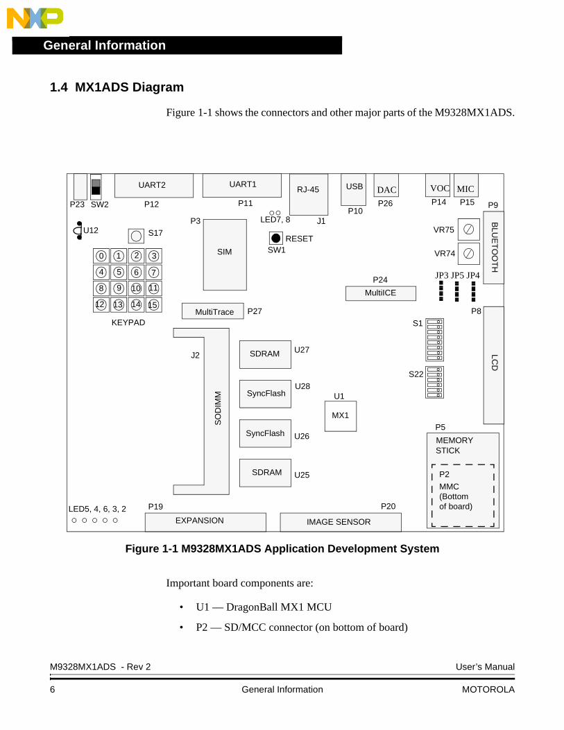
1.4 MX1ADS Diagram
Figure 1-1 shows the connectors and other major parts of the M9328MX1ADS.
Figure 1-1 M9328MX1ADS Application Development System
Important board components are:
• U1 — DragonBall MX1 MCU
• P2 — SD/MCC connector (on bottom of board)
P11
S1
S22
U12
P8
P24
SW1
J2
P19
P3
P27
SIM
LED7, 8VR75
VR74
LED5, 4, 6, 3, 2
SO
DIM
M
S17
MultiTrace
P15
J1
P26P10
P9
USBRJ-45
P23 P12
KEYPAD
P20
RESET
SW2 P14
UART1UART2
BLU
ET
OO
TH
LCD
MultiICE
P5
MEMORYSTICK
IMAGE SENSOREXPANSION
U27
U28
U26
U25
SDRAM
SDRAM
SyncFlash
SyncFlash
MX1
U1
5
0 1 2 3
4 6 7
8 9 10 11
12 13 14 15
P2
MMC (Bottom of board)
VOC MICDAC
JP3 JP5 JP4
M9328MX1ADS - Rev 2 User’s Manual
6 General Information MOTOROLA

General InformationMX1ADS Diagram
• P3 — SIM card connector
• P5 — Memory Stick connector
• P8 — LCD/touch panel connector
• P9 — BlueTooth connector
• P10 — USB connector
• P11, P12 — RS232 connectors to on chip UARTs
• P14, P15, P26 — voice out, microphone in, and DAC out connectors
• P19 — I/O expansion connector
• P20 — image sensor connector
• P23 — 3.0-volt input power connector
• P24 — ARM MultiICE connector
• P27 — ARM MutliTrace connector
• J1 — RJ-45 Ethernet connector
• J2 — Custom SODIMM memory expansion connector
• S1 — peripherals enable switches
• S5 - S16, S18 - S21 — 16 push button keypad keys
• S17 — General function push button switch
• S22 — boot and big/little endian mode select switch
• SW1 — reset switch
• SW2 — power switch
• LED2 and LED3 — general-purpose LEDs (yellow)
• LED4 — external bus activity LED (red)
• LED5 — power LED (green)
• LED6 — Bluetooth activity LED (yellow)
• LED7, LED8 — Ethernet activity LEDs (green, orange)
• U12 — IrDA transceiver
User’s Manual M9328MX1ADS - Rev 2
MOTOROLA General Information 7
General Information
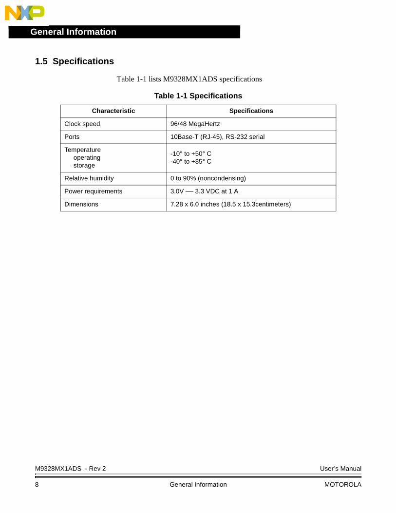
1.5 Specifications
Table 1-1 lists M9328MX1ADS specifications
Table 1-1 Specifications
Characteristic Specifications
Clock speed 96/48 MegaHertz
Ports 10Base-T (RJ-45), RS-232 serial
Temperature operating storage
-10° to +50° C-40° to +85° C
Relative humidity 0 to 90% (noncondensing)
Power requirements 3.0V — 3.3 VDC at 1 A
Dimensions 7.28 x 6.0 inches (18.5 x 15.3centimeters)
M9328MX1ADS - Rev 2 User’s Manual
8 General Information MOTOROLA

User’s Manual — M9328MX1ADS
Section 2 Configuration and Operation
2.1 Introduction
This section consists of configuration information, connection descriptions, and other operational information that may be useful in your development activities.
2.2 Configuring Board Components
Table 2-1 is a summary of configuration settings; subsections 2.2.1 through 2.2.2 give additional information.
Table 2-1 Component Configuration Settings
Component Position Effect
System Power Switch, SW2
Move this switch to the ON position to enable the power source connected to P23 to power the system.
Factory setting is OFF.
System Reset Switch, SW1
Push to reset the MX1ADS.
Peripheral Selection Switch, S1
S1 Enables UART1 transceiver, UART2 transceiver,and buzzer. Disables IrDA module.
Factory setting is shown.
Subsection 2.2.1 explains other settings for this switch.
SW2
ONOFFBRDEDGE
SW1
5
ON
48
S1
12
36
7
User’s Manual M9328MX1ADS - Rev 2
MOTOROLA Configuration and Operation 9

Configuration and Operation
2.2.1 Peripheral Selection Switch (S1)
Switch S1 enables or disables the UART transceivers, the IRDA buffers, and the buzzer.
Table 2-2 lists the functionality of these subswitches.
.
Mode Switch, S22 S22 Configures 32-bit SyncFlash as the boot device, configures Little Endian mode, and Normal mode operation.
Factory setting is shown
Subsection 2.2.2 explains other settings for this switch.
Table 2-1 Component Configuration Settings (Continued)
Component Position Effect
5
ON
4
S22
12
36
Table 2-2 S1 Subswitch Settings
Subswitch, FunctionSettin
g Effect
S1-1, UART1 transceiver ON Forces the UART1 transceiver to be enabled.
OFF UART1_EN bit of U42 controls the UART1 transceiver. Active low.*
S1-2, UART2 transceiver ON Forces the UART2 transceiver to be enabled.**.
OFF UART2_EN bit of U42 controls the UART2 transceiver. Active low.*
S1-3, IrDA module ON Forces the IrDA module buffers to be enabled.**
OFF IrDA_EN bit of U42 controls the IrDA buffers. Active low.*
S1-4, LCD — No effect
S1-5, Buzzer ON Enables the buzzer to be controlled by the PWMO output.
OFF PMWO is disconnected from the buzzer circuit.
S1-6, PEN_CS — No effect
S1-7, PEN_IRQ — No effect
S1-8 — No effect
M9328MX1ADS - Rev 2 User’s Manual
10 Configuration and Operation MOTOROLA
Configuration and OperationConfiguring Board Components
* Setting the associated bit high (power on reset default) disables the interface. Setting the bit low will enable the interface.
** Warning: Do not enable UART2 and IRDA at the same time. Neither circuit will function properly and circuit damage could result.
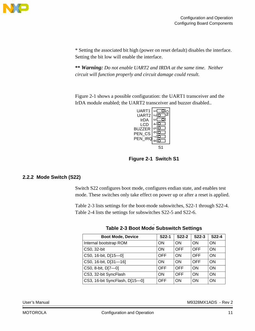
Figure 2-1 shows a possible configuration: the UART1 transceiver and the IrDA module enabled; the UART2 transceiver and buzzer disabled..
Figure 2-1 Switch S1
2.2.2 Mode Switch (S22)
Switch S22 configures boot mode, configures endian state, and enables test mode. These switches only take effect on power up or after a reset is applied.
Table 2-3 lists settings for the boot-mode subswitches, S22-1 through S22-4. Table 2-4 lists the settings for subswitches S22-5 and S22-6.
.
5
ON
48
BUZZER
IrDAUART2UART1
S1
12
36
7PEN_CSPEN_IRQ
LCD
Table 2-3 Boot Mode Subswitch Settings
Boot Mode, Device S22-1 S22-2 S22-3 S22-4
Internal bootstrap ROM ON ON ON ON
CS0, 32-bit ON OFF OFF ON
CS0, 16-bit, D[15—0] OFF ON OFF ON
CS0, 16-bit, D[31—16] ON ON OFF ON
CS0, 8-bit, D[7—0] OFF OFF ON ON
CS3, 32-bit SyncFlash ON OFF ON ON
CS3, 16-bit SyncFlash, D[15—0] OFF ON ON ON
User’s Manual M9328MX1ADS - Rev 2
MOTOROLA Configuration and Operation 11

Configuration and Operation
Warning: Do not select CPU Test mode. Nothing good will come of it.
Figure 2-2 shows a possible configuration:
• Subswitches S22-1 through S22-4 configure the boot mode to be CS0, 8-bit, D[7] through D[0].
• Subswitch S22-5 configures Little Endian mode.
• Subswitch S22-6 selects Normal mode.
Figure 2-2 Switch S22
Table 2-4 Subswitch S22-5, S22-6 Settings
Subswitch, Function Setting Effect
S22-5, Endian mode
ON Configures Little Endian mode.
OFF Configures Big Endian mode.
S22-6, CPU Mode ON Selects Normal mode.
OFF Selects CPU Test mode.
5
ON
4
TEST MODEENDIAN MODE
BOOT MODE
S22
12
36
M9328MX1ADS - Rev 2 User’s Manual
12 Configuration and Operation MOTOROLA
Configuration and OperationOperation
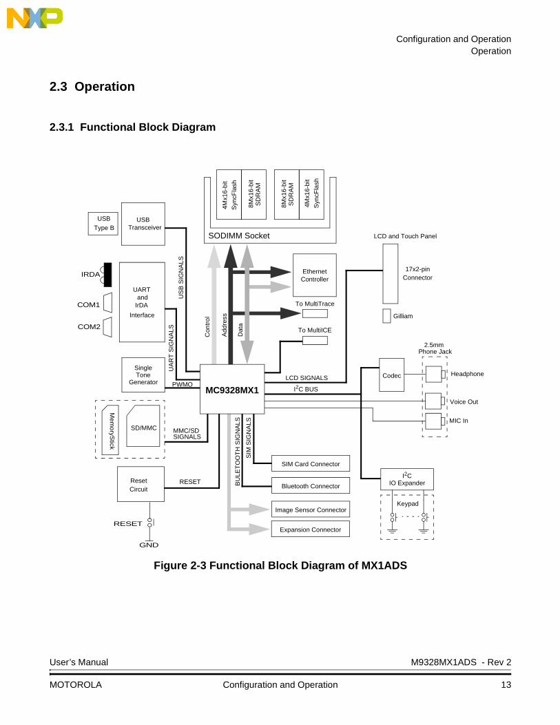
2.3 Operation
2.3.1 Functional Block Diagram
Figure 2-3 Functional Block Diagram of MX1ADS
SD/MMC
Mem
oryStick
Gilliam
LCD and Touch Panel
2.5mmPhone Jack
IRDA17x2-pin
Connector
UARTand
IrDA
Interface
To MultiTrace
Expansion Connector
Image Sensor Connector
Voice Out
MIC In
GND
RESET
ResetCircuit
EthernetController
To MultiICE
SODIMM Socket
MC9328MX1
4Mx1
6-bi
t
Syn
cFla
sh
4Mx1
6-bi
t
Syn
cFla
sh
8Mx1
6-bi
tS
DR
AM
Con
trol
Dat
a
Add
ress
8Mx1
6-bi
tS
DR
AM
SingleTone
Generator
USB
Type BUSB
Transceiver
US
B S
IGN
ALS
UA
RT
SIG
NA
LS
PWMO
RESET
I2C BUS
LCD SIGNALS
MMC/SDSIGNALS
SIM
SIG
NA
LS
BU
LET
OO
TH
SIG
NA
LS
COM1
COM2
SIM Card Connector
Bluetooth Connector
I2CIO Expander
Keypad
Codec Headphone
User’s Manual M9328MX1ADS - Rev 2
MOTOROLA Configuration and Operation 13
Configuration and Operation
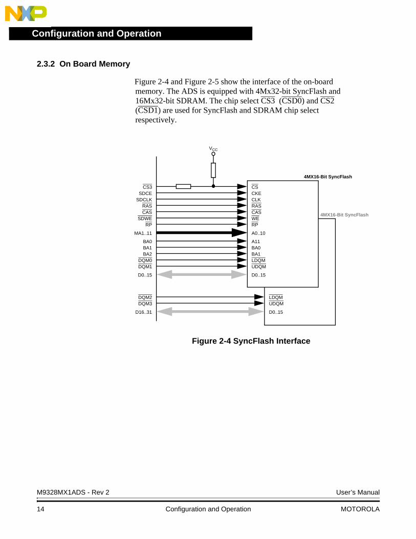
2.3.2 On Board Memory
Figure 2-4 and Figure 2-5 show the interface of the on-board memory. The ADS is equipped with 4Mx32-bit SyncFlash and 16Mx32-bit SDRAM. The chip select CS3 (CSD0) and CS2 (CSD1) are used for SyncFlash and SDRAM chip select respectively.
Figure 2-4 SyncFlash Interface
RASCAS
DQM0
SDWE
MA1..11
D0..15
SDCESDCLK
DQM1
RASCAS
UDQM
WE
A0..10
D0..15
4MX16-Bit SyncFlash
CS
CLKCKE
LDQM
4MX16-Bit SyncFlash
CS3
VCC
A11BA0BA1
BA0
BA2BA1
D0..15D16..31
UDQMLDQMDQM2
DQM3
RPRP
M9328MX1ADS - Rev 2 User’s Manual
14 Configuration and Operation MOTOROLA

Configuration and OperationOperation
Figure 2-5 SDRAM Interface
2.3.3 Memory Map
Table 2-5 represents the memory mapping for the external peripherals on the M9328MX1ADS board. Note the Sync Flash and the Ethernet Controller have repeated memory blocks due to the fact they do not take up the entire address space of the associated chip select. Software can access the same physical memory location at several different addresses. For instance SDRAM uses the entire 64 MB address space allowed for CSD0. The Sync Flash occupies only 16 MBs of the 64 MB space available to CSD1, so its memory is repeated 4 times. CS4 covers 16 MB allowing many repetitions of the Ethernet chip’s internal registers.
RASCAS
DQM0
SDWE
MA1..11
D0..15
SDCESDCLK
DQM1
RASCAS
UDQM
WE
A0..10
D0..15
16MX16-Bit SDRAM
CS
CLKCKE
LDQM
16MX16-Bit SDRAM
CS2
VCC
A11BA0BA1
BA0
BA2BA1
D0..15D16..31
UDQMLDQMDQM2
DQM3
User’s Manual M9328MX1ADS - Rev 2
MOTOROLA Configuration and Operation 15

Configuration and Operation
.
2.3.4 USB Interface
The USB Device Module of the MC9328MX1 interfaces the with a Phillips USB transceiver, PDIUSBP11A, connected to a USB type B connector, P10. For details on the operation of USB interface, please refer to MC9328MX1 data sheet. Figure 2-6 illustrates the USB interface connection.
Figure 2-6 USB Interface
Table 2-5 M9328MX1ADS Memory Map
PeripheralChip
SelectAddress Range (HEX) Act Mem Size
SDRAM CSD0 0x0800 0000 to 0x0BFF FFFF 64MB
SYNC FLASH CSD1 0x0C00 0000 to 0x0FFF FFFF 16MB
Ethernet Controller
CS4 0x1500 0000 to 0x15FF FFFF 16 BYTES
Internal SRAM NA 0x0030 0000 to 0x0031 FFFF 128 KB
PDIUSBP11A
USB Device USB Type B Connector
VCC
D+
D-
MC9328MX1
M9328MX1ADS - Rev 2 User’s Manual
16 Configuration and Operation MOTOROLA

Configuration and OperationOperation
2.3.5 UART and IrDA
Figure 2-7 shows how the UART and the IrDA circuits are connected.
Figure 2-7 UARTs and IrDA Interface
Buffer
EN
IRDA
EN
TXD1RXD1
CTS1RTS1
RS232 Transceiver J4
UART1EN
VCC
GND
S1-1
Software Enablevia I/O expander
TXD2RXD2
CTS2RTS2
RS232 Transceiver J5
UART2EN
VCC
GND
S1-2
Software Enablevia I/O expander
VCC
GND
S1-4
Software Enablevia I/O expander
User’s Manual M9328MX1ADS - Rev 2
MOTOROLA Configuration and Operation 17

Configuration and Operation
2.3.6 Ethernet
The M9328MX1ADS is equipped with Cirrus Logic CS8900A Crystal LAN ISA Ethernet Controller. The CS8900A has 10BaseT transmit and receive filters and can interface with the M9328MX1. The CS8900A is operating in I/O mode. Figure 2-8 shows an overview of the Ethernet interface.
Figure 2-8 Ethernet Interface
2.3.7 CD Quality DAC and Analog I/O
The M9328MX1ADS is equipped with Micronas Stereo Audio DAC. The DAC3350A, U32, is controlled by the MX1 which sends the DAC digital audio data via the I2C bus. The I2C slave address of the DAC3350A is 0x9A.
The DAC also provides volume control and a headphone amplifier output. This amplifier is connected to the P26 audio connector. A filtered low level audio output is connected to the JP3 header.
CS8900A
RJ45 Connector
Isolation Transformer
MC9328MX1
CS4
A1..3
D0..16
OE
WE
EB3
IRQ (PTC17)
SBHE
IOW
IOR
AEN
D0..16
INTRQ0
SA8SA9
SA0SA4..7SA10..19
SA1..3
VCC
CHIPSEL
M9328MX1ADS - Rev 2 User’s Manual
18 Configuration and Operation MOTOROLA

Configuration and OperationOperation
The mixing of external analog audio sources to the converted DAC signal is supported. These signals can be input at the JP4 and JP5 headers. Additionally the voice out signal from the MX1 is connected to the AUX1 input of the DAC3350A. This signal is also amplified and driven to a second headphone connector, P14.
The ADS also provides a microphone connector at P15. This input is suitable for dynamic microphones only. The microphone input signal level can be varied by VR74. The conditioned signal is then fed to the MIP input of the MX1.
Table 2-6 is a list of the audio connectors. All audio jacks are standard 3.5mm stereo connectors. Table 2-7 through Table 2-9 describe the header pin outs.
Table 2-6 Audio Connectors
Connector Descriptions
P26 Headphone jack for DAC3350A audio out.
P14 Headphone jack for MX1 Voice Out
P15 Dynamic microphone input jack
Table 2-7 Audio Header JP3 Signal Descriptions
Pin Mnemonic Signal
1 FINR Filtered op amp output right, line out
2,3 AGND Analog Ground
4 FINL Filtered op amp output left, line out
User’s Manual M9328MX1ADS - Rev 2
MOTOROLA Configuration and Operation 19

Configuration and Operation
* Note: The voice output from the MX1 also connects to both AUX1 channels causing them to be shorted. Remove zero ohm resistors R142 and R141 to break this connection.
For the details on the operation of DAC3550A, please refer to its data sheet. The data sheet is available on the web:
http://www.micronas.com/
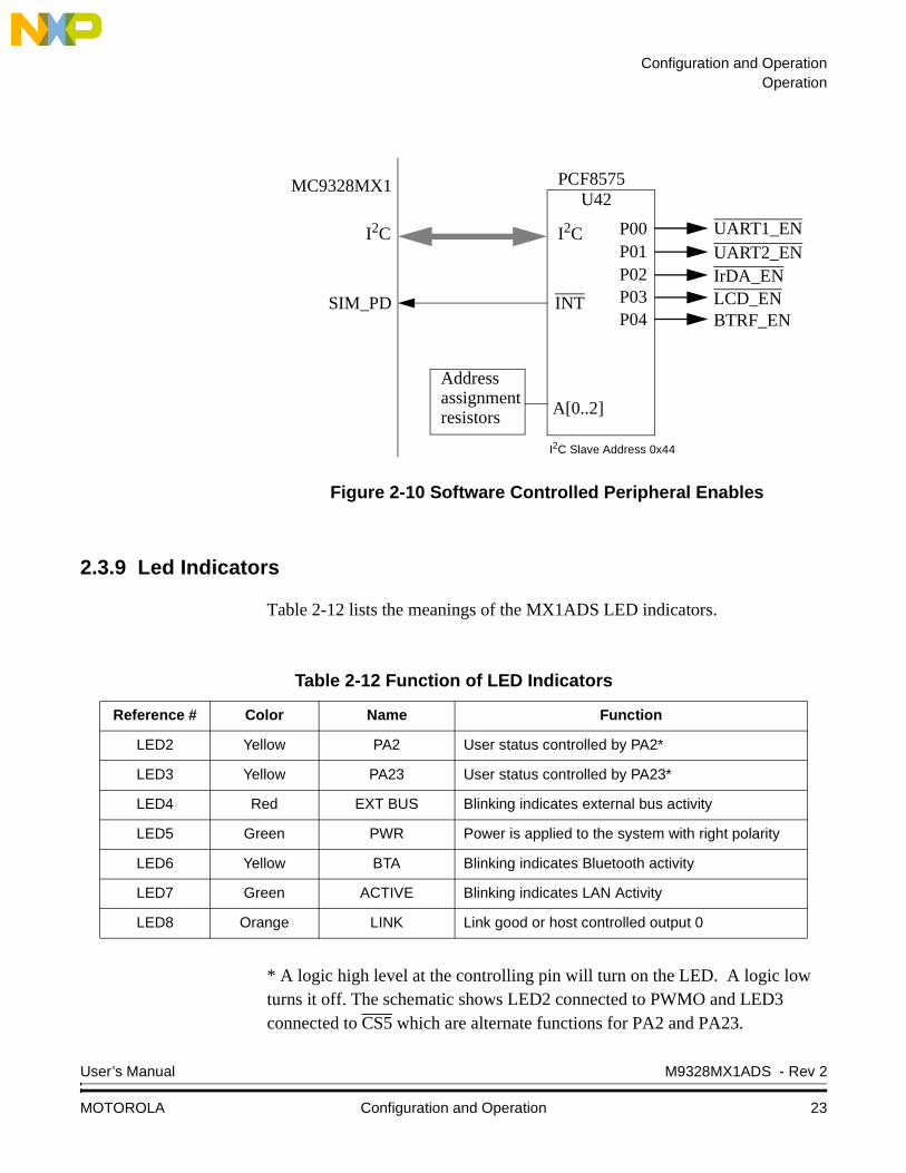
2.3.8 Keypads and IO Expander
The M9328MX1ADS is equipped with two Phillips PCF8575 I/O expanders. One is for the keypad array and the other is for peripheral control. The keypad array consist of a matrix of momentary push button switches mounted directly to the ADS board. Figure 2-9 and Table 2-10 shows the interface of the I/O expander to the keypads. The read slave address is 0x49. The PCF8575 can be used to generated an interrupt whenever a key is pressed or released. The interrupt signal is connected to the SIM_PD signal of the DBMX1 which should be configured as GPIO, PB15. There is an additional push button switch, S17, that is connected to the SPI_RDY signal of the DBMX1. That pin should be configured as GPIO, PC13, to use it with S17. When any switch is depressed it will cause a low (zero) to appear at the associated input pin. These switches have no hardware debounce so that function must be handled by the software.
Table 2-8 Audio Header JP4 Signal Descriptions
Pin Mnemonic Signal
1 AUX1R Auxiliary Input 1, right channel*
2,3 AGND Analog Ground
4 AUX1L Auxiliary Input 1, left channel*
Table 2-9 Audio Header JP5 Signal Descriptions
Pin Mnemonic Signal
1 AUX2R Auxiliary Input 2, right channel
2,3 AGND Analog Ground
4 AUX2L Auxiliary Input 2, left channel
M9328MX1ADS - Rev 2 User’s Manual
20 Configuration and Operation MOTOROLA

Configuration and OperationOperation
Table 2-11 and Figure 2-10 shows the interface to software controlled periph-eral enables. Peripherals can be enable or disable by programming the I/O expander. This depends on the state of the associated enable switch (S1) which can override software control. The write slave address is 0x44 and the read address is 0x45.
The PCF8575 consists of a 16-bit quasi-bidirectional port and an I2C-bus inter-face. On power up all pins are configured as inputs. A non power up reset has no effect on the PCF8575 which communicates with the MC9328MX1 through
the I2C interface. For the details on the operation of PCF8575, please refer to its data sheet. The data sheet is available on the web:
http://www.semiconductors.philips.com
Figure 2-9 Keypads and I/O Expander Interface
PCF8575
I2C I2C
INTSIM_PD
A[0..2]
I/O
Keypads
MC9328MX1
I2C Slave Address 0x48
Addressassignmentresistors
U33
User’s Manual M9328MX1ADS - Rev 2
MOTOROLA Configuration and Operation 21

Configuration and Operation
Table 2-10 Keypad I/O Expander InterfaceI/O Expander
PortKey Read
I/O Expander Port
Key Read
P00 Key 0 / S8 P10 Key 8 / S16
P01 Key 1 / S7 P11 Key 9 / S15
P02 Key 2 / S6 P12 Key 10 / S14
P03 Key 3 / S5 P13 Key 11 / S13
P04 Key 4 / S12 P14 Key 12 / S21
P05 Key 5 / S11 P15 Key 13 / S20
P06 Key 6 / S10 P16 Key 14 / S19
P07 Key 7 / S9 P17 Key 15 / S18
Table 2-11 I/O Expander to Peripherals (U42)
I/O Expander Port Mnemonic Signal
P00 UART1_EN UART1 enable
P01 UART2_EN* UART2 enable*
P02 IrDA_EN* IrDA enable*
P03 LCD_ON Not used (reserved)
P04 BTRF_EN Not used (reserved)
P05,P06,P07,P12-P17
NC NO CONNECTION
P10 SD_WP Secure Data Write Protect
P11 SD_CD Secure Data Card Detect
M9328MX1ADS - Rev 2 User’s Manual
22 Configuration and Operation MOTOROLA
Configuration and OperationOperation
Figure 2-10 Software Controlled Peripheral Enables
2.3.9 Led Indicators
Table 2-12 lists the meanings of the MX1ADS LED indicators.
* A logic high level at the controlling pin will turn on the LED. A logic low turns it off. The schematic shows LED2 connected to PWMO and LED3 connected to CS5 which are alternate functions for PA2 and PA23.
PCF8575
I2C I2C
INTSIM_PD
A[0..2]
P00
MC9328MX1
P01P02P03P04
UART1_ENUART2_ENIrDA_ENLCD_ENBTRF_EN
I2C Slave Address 0x44
U42
Addressassignmentresistors
Table 2-12 Function of LED Indicators
Reference # Color Name Function
LED2 Yellow PA2 User status controlled by PA2*
LED3 Yellow PA23 User status controlled by PA23*
LED4 Red EXT BUS Blinking indicates external bus activity
LED5 Green PWR Power is applied to the system with right polarity
LED6 Yellow BTA Blinking indicates Bluetooth activity
LED7 Green ACTIVE Blinking indicates LAN Activity
LED8 Orange LINK Link good or host controlled output 0
User’s Manual M9328MX1ADS - Rev 2
MOTOROLA Configuration and Operation 23

Configuration and Operation
2.4 Using The Board Connectors
Table 2-13 lists the MX1ADS connectors, explaining their function, and any special instructions for using the connector. Figure 1-1 shows the connector locations on the board along with their reference designators.
Table 2-13 MX1ADS Connectors
Connector Purpose Comments
J1 Ethernet Standard Ethernet connector. A cable for direct network and one for crossover connections (direct to a PC) have been provided in the m9328MX1ESBP Professional Edition.
J2 SODIMM Slide SODIMM card into the connector until it snaps into place. Not compatible with off the shelf DIMM modules.
JP3 FOUTR, FOUTL Filtered output of right and left channels from the DAC3550A.
JP4 AUX1R, AUX1L, Auxiliary audio input channel 1 with left and right stereo inputs. Compatible with low level outputs of most audio electronics.
JP5 AUX2R, AUX2L Auxiliary audio input channel 2 with left and right stereo inputs. Compatible with low level outputs of most audio electronics.
P2 SD/MMC Connector is on bottom of board, directly below the P5 memory stick connector. Slide the MMC unit into the connector until it snaps into place. Shares signals with the Memory Stick card interface.
P3 SIM Unsnap latch, swing lid up. Slide SIM card inside, matching alignment of contacts at the connector base. Close the lid and push down to latch.
P5 Memory Stick Slide the memory stick into the connector until it snaps into place. Shares signals with the SD/MMC card interface.
P8 LCD panel Connect LCD ribbon cable between this connector and the corresponding connector of the LCD display panel, J11.
P9 BlueTooth module Connect a compatible Bluetooth daughter board into this connector. A MMM7400 Bluetooth module is included in the M9328MX1ESBP kit.
M9328MX1ADS - Rev 2 User’s Manual
24 Configuration and Operation MOTOROLA

Configuration and OperationAdd On Module Connections and Usage
* For information on ARM supplied devices that are compatible with these connectors please visit ARM’s web site at: http://www.arm.com
2.5 Add On Module Connections and Usage
2.5.1 Using the TFT LCD Display Panel
Your MX1ADS and MX1ESBP come equipped with a touch control enabled TFT (Thin Film Transistor) LCD display assembly. The TFT LCD component is from Sharp Corporation, model number LQ035Q2DD54. A detailed specification has been included on the documentation CD that came with your ADS.
P10 USB Standard USB connector.
P11 UART1 Standard DB9 connector set up for DCE operation.
P12 UART2 Standard DB9 connector set up for DCE operation.
P14 Voice Out Standard 3.5 mm connector for stereo audio.This is the output of the amplified voice out from the MC9328MX1 suitable for use with standard headphones with a 16 to 32 ohms impedance.
P15 Microphone Standard 3.5 mm connector for stereo audio. Use only dynamic microphones with a 200 to 600 ohms impedance.
P19 Expansion Standard 48 pin, three row, male DIN connectors. Can connect directly or be cabled to a custom circuit board.
P20 Image sensor Connect image-sensor daughter board to this connector, then connect ribbon cable and lens board to the daughter board.
P23 Power Plug the 3-volt power-supply jack end into this connector.
P24 MultiICE Standard ARM MultiICE connector.*
P26 Headphone Standard 3.5 mm connector for stereo audio. This is the amplified stereo output of the DAC3550A. Use headphones with a 16 to 32 ohms impedance.
P27 MultiTrace Standard ARM MultiTrace connector.*
Table 2-13 MX1ADS Connectors (Continued)
Connector Purpose Comments
User’s Manual M9328MX1ADS - Rev 2
MOTOROLA Configuration and Operation 25
Configuration and Operation
To begin using your MX1ADS LCD module you must connect the 34 conductor ribbon cable (RE11057C) that came with your MX1ADS between connectors J11 on the LCD module and P8 on the MX1ADS main board.
Warning: Be sure input power to the main board is disconnected or switched off before the LCD module is connected. Connecting the module with power applied could damage the LCD module and/or the main board.
Your TFT LCD module has two variable resistors that allow users to vary the contrast, sometimes described as view angle, and the brightness of the FL backlight. Adjustment of VR1 will change the contrast and VR4 controls the backlight brightness. These potentiometers are recessed below the Plexiglas cover. You will need to use a suitable flat head or phillips head screwdriver to adjust them. This may be done with power applied but caution is advised when using a metal tool. A plastic bladed tools is recommend. While these controls were set at the factory, adjustment may be required to suit the user’s preferences.
2.5.2 Using a SODIMM Card
This connector provide a way to add new circuit boards that may be developed in the future. Users can also develop compatible DIMM cards as well.
Caution should be used when developing such boards to avoid addressing conflicts with peripherals that already exits on the main board.
Warning: To avoid circuit damage, do not plug in SODIMM cards with power applied to the board.
2.5.3 Using a SIM, SD/MMC, or Memory Stick Card
The users must obtain their own compatible cards for use with these connectors. Please note the power is connected to VCC which is 3.0-volts when using the power supply provide with your kit.
Warning: To avoid circuit damage, do not plug in SIM, SD/MMC, or Memory Stick cards with power applied to the board.
M9328MX1ADS - Rev 2 User’s Manual
26 Configuration and Operation MOTOROLA

Configuration and OperationAdd On Module Connections and Usage
2.5.4 Using the BlueTooth Daughter Board
This connector, P9, comes configured to operate directly with the Motorola MMM7400 Bluetooth RF module that is included in the M9328MX1ESBP. There are zero ohm resistor components that may be removed and/or added to change what signals are connected. This can be used to adapt the connector to other RF modules from other vendors. Software to control this interface using the MMM7400 may be found at the following web site:
http://www.motorola.com/dragonball
Warning: To avoid circuit damage, do not plug in a Bluetooth module with power applied to the board.
2.5.5 Using the Image Sensor daughter boards
This connector comes configured to operate directly with the CSI Daughter Card that is included in the M9328MX1ESBP. The communication with this card takes place through the I2C interface. Refer to the specification for the SMC20014 included on the user documentation CD for information on how to use this device.
To install the image sensor boards, first locate the TetraCam sensor board. Plug its J1 connector into the J1 connector of the CSI Daughter Card. Make sure that JP1 has a jumper installed and that JP2 does not. Plug the 48 position DIN connect on the back side of the CSI daughter card into P20 of the main board. The two boards will be at a right angle to each other with the image sensor facing away from the main board.
Warning: To avoid circuit damage, do not plug in the TetraCam Image Sensor or CSI daughter card with power applied to the board.
User’s Manual M9328MX1ADS - Rev 2
MOTOROLA Configuration and Operation 27
Configuration and Operation
M9328MX1ADS - Rev 2 User’s Manual
28 Configuration and Operation MOTOROLA
User’s Manual — M9328MX1ADS
Section 3 Support Information
3.1 Introduction
This section consists of connector pin assignments, connector signal descriptions, and other information that may be useful in your development activities.
3.2 S.O.DIMM Socket
Connector J2 is the MX1ADS SODIMM connector. Figure 3-1 gives pin assignments for this connector and Table 3-1 gives signal descriptions for this connector. Please note this in not an industry standard pin out and that it is unlikely to be compatible with off the self DIMM cards
User’s Manual M9328MX1ADS - Rev 2
MOTOROLA Support Information 29
Support Information
.
J2GND 1 • • 2 GND
D0 3 • • 4 ~EB0D1 5 • • 6 ~EB1D2 7 • • 8 ~EB2D3 9 • • 10 ~EB3
VCC 11 • • 12 VCCD4 13 • • 14 ~OED5 15 • • 16 ~WED6 17 • • 18 ~ECBD7 19 • • 20 ~LBA
GND 21 • • 22 GNDDQM0 23 • • 24 A0DQM1 25 • • 26 A1
VCC 27 • • 28 VCCA2 29 • • 30 A5A3 31 • • 32 A6A4 33 • • 34 A7
GND 35 • • 36 GNDD8 37 • • 38 ~BAAD9 39 • • 40 ~BCLK
D10 41 • • 42 NCD11 43 • • 44 NC
VCC 45 • • 46 VCCD12 47 • • 48 ~CS0D13 49 • • 50 ~CS1D14 51 • • 52 ~CS4D15 53 • • 54 ~CS5
GND 55 • • 56 GND~RESETSF 57 • • 58 MOSI
MISO 59 • • 60 SSSDCLK 61 • • 62 SDCKE0
VCC 63 • • 64 VCC~RAS 65 • • 66 ~CAS
~SDWE 67 • • 68 SDCKE1~CS2 69 • • 70 A13~CS3 71 • • 72 SPI_RDY
~RESET 73 • • 74 SDCLKGND 75 • • 76 GND
CLKOUT 77 • • 78 SIM_TXNC 79 • • 80 SIM_RX
VCC 81 • • 82 VCC
M9328MX1ADS - Rev 2 User’s Manual
30 Support Information MOTOROLA

Support InformationS.O.DIMM Socket
Figure 3-1 SODIMM Connector J2 Pin Assignments
*These connector pins may be connected to address lines with the addition of a zero ohm resistor. For more details please refer to the M9328MX1ADS schematic, sheet 10 of 12.
D16 83 • •• •• •• •• •• •• •• •• •• •• •• •• •• •• •• •• •• •• •• •• •• •• •• •• •• •• •• •• •• •• •
84 SIM_SVEND17 85 86 SIM_PDD18 87 88 SIM_CLKD19 89 90 SIM_RST
GND 91 92 GNDD20 93 94 A16D21 95 96 A17D22 97 98 A18D23 99 100 A19VCC 101 102 VCC
A8 103 104 A9A10 105 106 NC*
GND 107 108 GNDMA10 109 110 NC*MA11 111 112 NC*VCC 113 114 VCC
DQM2 115 116 A11DQM3 117 118 A12
GND 119 120 GNDD24 121 122 A14D25 123 124 A15D26 125 126 A20D27 127 128 A21VCC 129 130 VCCD28 131 132 A22D29 133 134 A23D30 135 136 A24D31 137 138 NC
GND 139 140 GNDNC 141 142 NC
VCC 143 144 VCC
Table 3-1 SODIMM Connector J2 Signal Descriptions
Pin Mnemonic Signal
1, 2, 21, 22, 35, 36, 55, 56, 75, 76, 91, 92, 107, 108, 119, 120,
139, 140
GND GROUND
User’s Manual M9328MX1ADS - Rev 2
MOTOROLA Support Information 31

Support Information
3, 5, 7, 9, 13, 15, 17, 19, 37, 39, 41, 43, 47, 49, 51, 53, 83, 85, 87, 89, 93, 95, 97, 99, 121, 123, 125, 127, 131, 133, 135,
137
D0 — D31 DATA BUS (lines 0—31) — Bidirectional signals for transferring data between the processor and an external device.
4, 6, 8, 10 ~EB0 — ~EB3 ENABLE BYTE (lines 0—3) — Active-low outputs that indicate active data bytes for the current access. ~EB0 corresponds to DATA[31—24], ~EB1 corresponds to DATA[23—16], ~EB2 corresponds to DATA[15—8], and ~EB3 corresponds to DATA[7—0]
11, 12, 27, 28, 45, 46, 63, 64, 81, 82, 101,
102, 113, 114, 129, 130, 143,
144
VCC VCC (3.0-volts)
14 ~OE OUTPUT ENABLE — Active-low output that indicates that a bus access is a read access; enables slave devices to drive the data bus.
16 ~WE WRITE ENABLE — Active-low output
18 ~ECB END CURRENT BURST — Active-low input signal asserted by external burst devices; indicates the end of a burst sequence
20 ~LBA LOAD BURST ADDRESS — Active-low signal asserted during burst mode accesses; causes the external burst device to load a new starting burst address
23, 25, 115, 117 DQM0 — DQM3 SDRAM enable bytes (0-3) - Active-low output signals.
24, 26, 29 — 34, 70, 94, 96, 98, 100, 103 — 105, 116, 118, 122, 124, 126, 128, 132, 134,
136
A{0 — A24 (not in exact
order)
ADDRESS BUS (0-24) - Output lines for addressing external devices.
38 ~BAA BURST ADDRESS ADVANCE — Active-low signal asserted during burst mode accesses; causes the external burst devices to increment internal burst counters.
40 ~BCLK BURST CLOCK — Output signal to external burst devices; synchronizes burst loading and incrementing
42, 44, 77, 79, 106, 110, 112, 138, 141, 142
NC NO CONNECTION
Table 3-1 SODIMM Connector J2 Signal Descriptions (Continued)
Pin Mnemonic Signal
M9328MX1ADS - Rev 2 User’s Manual
32 Support Information MOTOROLA

Support InformationUART Connectors
3.3 UART Connectors
Connectors P11 and P12 are the MX1ADS UART connectors. Figure 3-2 gives the pin assignments and Table 3-2 gives the signal descriptions for UART1 connector P11 and UART2 connector P12.
48, 50, 52, 54, 69, 71
~CS0 — ~CS5 (not in exact
order)
CHIP SELECTS (lines 0 - 5) - Chip-select signals, active-low outputs.
57 ~RESETSF RESET SYNC FLASH - Active low output
58 MOSI MASTER OUT / SLAVE IN - SPI data signal (bidirectional)
59 MISO MASTER IN / SLAVE OUT - SPI data signal (bidirectional)
60 SS SLAVE SELECT - bidirectional, active low, input in slave mode, output in master mode
61, 74 SDCLK SDRAM clock - output to SDRAM
62, 68 SDCKE0, SDCKE1
SDRAM CLOCK ENABLE 0 & 1 - Active high outputs to SDRAM
65 ~RAS ROW ADDRESS STROBE -clocks row address to SDRAM
66 ~CAS COLUMN ADDRESS STROBE - clocks column address to SDRAM
67 SDWE SDRAM WRITE ENABLE - write data strobe to SDRAM, active low
72 SPI_RDY SPI READY - CSPI serial burst trigger, active low input
73 ~RESET RESET — Active-low reset signal to the processor
78,80 SIM_TX,SIM_RX SIM TRANSMITTED/ SIM RECEIVED DATA - SIM card data, tied together externally through zero ohm resistor.
84 SIM_SVEN SIM VCC ENABLE - enable power to the SIM card, active low
86 SIM_PD SIM PRESENCE DETECT - Active low input
88 SIM_CLK SIMCLOCK - output clock to SIM card
90 SIM_RST SIM RESET - Active low output to SIM card
109, 111 MA10, MA11 MUXED ADDRESS 10 & 11 - Multiplexed addresses to SDRAM
Table 3-1 SODIMM Connector J2 Signal Descriptions (Continued)
Pin Mnemonic Signal
User’s Manual M9328MX1ADS - Rev 2
MOTOROLA Support Information 33
Support Information
Figure 3-2 Connector P11 (UART1), P12 (UART2) Pin Assignments
Waning: UART2 can not be used if IrDA is enabled.
3.4 MultiICE Connector
Connector P24 is the MX1ADS MultiICE connector. Figure 3-3 gives the pin assignments and Table 3-3 gives the signal descriptions for this connector.
1
RXDTX
D
NCCTSRTS NC
P11 or P12
2345
9 8 7 6
NCGND
NC
Table 3-2 Connector P11 (UART1), P12 (UART2) Signal Descriptions
Pin Mnemonic Signal
1, 4, 6, 9 NC NO CONNECTION
2 TXD TRANSMITTED DATA — RS232 serial data output signal.
3 RXD RECEIVED DATA – RS232 serial data input signal.
5 GND GROUND
7 RTS READY TO SEND — Active-positive, RS232 input signal.
8 CTS CLEAR TO SEND — Active-positive RS232 output signal.
M9328MX1ADS - Rev 2 User’s Manual
34 Support Information MOTOROLA

Support InformationEthernet Connector
Figure 3-3 MultiICE Connector P24 Pin Assignments
3.5 Ethernet Connector
Connector J1 is the RJ-45 MX1ADS Ethernet connector. Figure 3-4 gives the pin assignments and Table 3-4 gives the signal descriptions for this connector.
P24VCC 1 • • 2 VCC
~TRST 3 • • 4 GND
TDI 5 • • 6 GND
TMS 7 • • 8 GND
TCK 9 • • 10 GND
GND 11 • • 12 GND
TDO 13 • • 14 GND
~RESET 15 • • 16 GND
NC 17 • • 18 GND
NC 19 • • 20 GND
Table 3-3 MultiICE Connector P24 Signal Descriptions
Pin Mnemonic Signal
1, 2 VCC 3.0-VOLT POWER
3 ~TRST TARGET RESET — Active-low output signal that resets the target.
4, 6, 8, 10 — 12, 14, 16, 18,
20
GND GROUND
5 TDI TEST DATA INPUT — Serial data output line, sampled on the rising edge of the TCK signal.
7 TMS TEST MODE SELECT – Output signal that sequences the target’s JTAG state machine, sampled on the rising edge of the TCK signal.
9 TCK TEST CLOCK — Output timing signal, for synchronizing test logic and control register access.
13 TDO JTAG TEST DATA OUTPUT — Serial data input from the target.
15 ~RESET RESET — Active-low reset signal.
17, 19 NC NO CONNECTION
User’s Manual M9328MX1ADS - Rev 2
MOTOROLA Support Information 35
Support Information
Figure 3-4 Ethernet Connector J1 Pin Assignments
3.6 USB Connector
Connector P10 is the USB connector. Figure 3-5 gives the pin assignments and Table 3-5 gives the signal descriptions for this connector.
.
Figure 3-5 USB Connector P10 Pin Assignments
1
Table 3-4 Ethernet Connector J1 Signal Descriptions
Pin Mnemonic Signal
1 TPO+ DIFFERENTIAL OUTPUT PLUS
2 TPO- DIFFERENTIAL OUTPUT MINUS
3 TPI+ DIFFERENTIAL INPUT PLUS
4, 5, 7, 8 NC NO CONNECTION
6 TPI- DIFFERENTIAL INPUT MINUS
9,10 GND GROUND
3 4
2 1
Table 3-5 USB Connector P10 Signal Descriptions
Pin Mnemonic Signal
1 NC NO CONNECTION
2 D- USB DATA MINUS
M9328MX1ADS - Rev 2 User’s Manual
36 Support Information MOTOROLA
Support InformationBlueTooth Connector
3.7 BlueTooth Connector
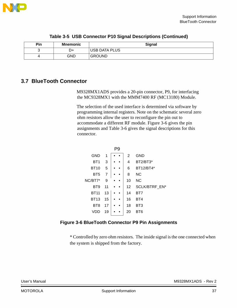
M9328MX1ADS provides a 20-pin connector, P9, for interfacing the MC9328MX1 with the MMM7400 RF (MC13180) Module.
The selection of the used interface is determined via software by programming internal registers. Note on the schematic several zero ohm resistors allow the user to reconfigure the pin out to accommodate a different RF module. Figure 3-6 gives the pin assignments and Table 3-6 gives the signal descriptions for this connector.
Figure 3-6 BlueTooth Connector P9 Pin Assignments
* Controlled by zero ohm resistors. The inside signal is the one connected when the system is shipped from the factory.
3 D+ USB DATA PLUS
4 GND GROUND
Table 3-5 USB Connector P10 Signal Descriptions (Continued)
Pin Mnemonic Signal
P9GND 1 • • 2 GND
BT1 3 • • 4 BT2/BT3*
BT10 5 • • 6 BT12/BT4*
BT5 7 • • 8 NC
NC/BT7* 9 • • 10 NC
BT9 11 • • 12 SCLK/BTRF_EN*
BT11 13 • • 14 BT7
BT13 15 • • 16 BT4
BT8 17 • • 18 BT3
VDD 19 • • 20 BT6
User’s Manual M9328MX1ADS - Rev 2
MOTOROLA Support Information 37
Support Information
3.8 MultiTrace Connector
Connector P27 is the MX1ADS MultiTrace connector. Figure3-7 gives the pin assignments and Table 3-7 gives the signal descriptions for this connector.
Table 3-6 BlueTooth Connector P9 Signal Descriptions
Pin Mnemonic Signal
1, 2 BTRF GND GROUND for BT RF module
3 BT1 Ref_Clk (24Mhz)
4 BT2 Transmit Data
5 BT10 Inverse BT_RF_OSC_EN/GPO2
6 BT12 SPI data out
7 BT5 Frame synch
8, 10 NC NO CONNECTION
9,14 BT7 Diversity/BT_RF_OSC_EN
11 BT9 RxTx_en/HOP_SRB
12 SCLK Should be configured as GPIO, PC14
13 BT11 SPI enable
15 BT13 SPI clock
16 BT4 SPI data in
17 BT8 PWM_RSSI/TXEN
18 BT3 Receive Data
19 BTRF VDD Power supply for BT RF module
20 BT6 PWM_Tx/GPO1
M9328MX1ADS - Rev 2 User’s Manual
38 Support Information MOTOROLA

Support InformationMultiTrace Connector
Figure 3-7 MultiTrace Connector P27 Pin Assignments
P27
NC 1 • • 2 NC
NC 3 • • 4 NC
GND 5 • • 6 A23
NC 7 • • 8 NC
~RESET 9 • • 10 NC
TDO 11 • • 12 VCC
NC 13 • • 14 NC
TCLK 15 • • 16 ~ECB
TMS 17 • • 18 ~LBA
TDI 19 • • 20 ~BCLK
~TRST 21 • • 22 ~BAA
GND 23 • • 24 A19
GND 25 • • 26 A18
GND 27 • • 28 A17
GND 29 • • 30 A16
GND 31 • • 32 A24
GND 33 • • 34 A22
GND 35 • • 36 A21
GND 37 • • 38 A20
Table 3-7 MultiTrace Connector P27 Signal Descriptions
Pin Mnemonic Signal
1 — 4, 7, 8, 10, 13, 14,
NC NO CONNECTION
5, 23, 25, 27, 29, 31, 33, 35,
37
GND GROUND
6, 24, 26, 28, 30, 32, 34, 36,
38
A16 — A24 (not in exact
order)
ADDRESS BUS (lines 16—24) — Output lines for addressing external devices.
9 ~RESET RESET — Active-low reset signal.
11 TDO JTAG TEST DATA OUTPUT — Serial data input from the target
12 VCC 3.3-VOLT POWER
15 TCLK TEST CLOCK — Output timing signal, for synchronizing test logic and control register access.
User’s Manual M9328MX1ADS - Rev 2
MOTOROLA Support Information 39

Support Information
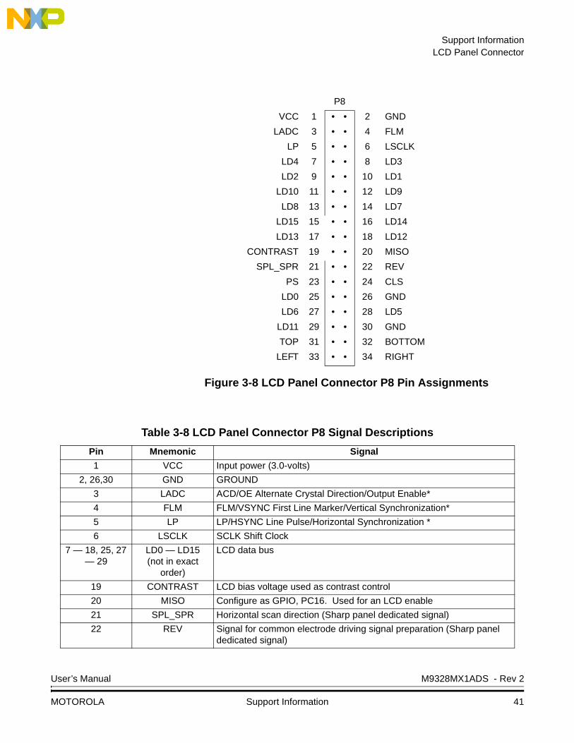
3.9 LCD Panel Connector
Connector P8 is the MX1ADS LCD panel connectors. Figure 3-8 gives the pin assignments and Table 3-8 gives the signal descriptions this connector.
16 ~ECB END CURRENT BURST — Active-low input signal asserted by external burst devices; indicates the end of a burst sequence.
17 TMS TEST MODE SELECT – Output signal that sequences the target’s JTAG state machine, sampled on the rising edge of the TCK signal.
18 ~LBA LOAD BURST ADDRESS — Active-low signal asserted during burst mode accesses; causes the external burst device to load a new starting burst address.
19 TDI TEST DATA INPUT — Serial data output line, sampled on the rising edge of the TCK signal.
20 ~BCLK BURST CLOCK — Output signal to external burst devices; synchronizes burst loading and incrementing.
21 ~TRST TARGET RESET — Active-low output signal that resets the target.
22 ~BAA BURST ADDRESS ADVANCE — Active-low signal asserted during burst mode accesses; causes the external burst devices to increment internal burst counters.
Table 3-7 MultiTrace Connector P27 Signal Descriptions (Continued)
Pin Mnemonic Signal
M9328MX1ADS - Rev 2 User’s Manual
40 Support Information MOTOROLA
Support InformationLCD Panel Connector
Figure 3-8 LCD Panel Connector P8 Pin Assignments
P8
VCC 1 • • 2 GND
LADC 3 • • 4 FLM
LP 5 • • 6 LSCLK
LD4 7 • • 8 LD3
LD2 9 • • 10 LD1
LD10 11 • • 12 LD9
LD8 13 • • 14 LD7
LD15 15 • • 16 LD14
LD13 17 • • 18 LD12
CONTRAST 19 • • 20 MISO
SPL_SPR 21 • • 22 REV
PS 23 • • 24 CLS
LD0 25 • • 26 GND
LD6 27 • • 28 LD5
LD11 29 • • 30 GND
TOP 31 • • 32 BOTTOM
LEFT 33 • • 34 RIGHT
Table 3-8 LCD Panel Connector P8 Signal Descriptions
Pin Mnemonic Signal
1 VCC Input power (3.0-volts)
2, 26,30 GND GROUND
3 LADC ACD/OE Alternate Crystal Direction/Output Enable*
4 FLM FLM/VSYNC First Line Marker/Vertical Synchronization*
5 LP LP/HSYNC Line Pulse/Horizontal Synchronization *
6 LSCLK SCLK Shift Clock
7 — 18, 25, 27 — 29
LD0 — LD15(not in exact
order)
LCD data bus
19 CONTRAST LCD bias voltage used as contrast control
20 MISO Configure as GPIO, PC16. Used for an LCD enable
21 SPL_SPR Horizontal scan direction (Sharp panel dedicated signal)
22 REV Signal for common electrode driving signal preparation (Sharp panel dedicated signal)
User’s Manual M9328MX1ADS - Rev 2
MOTOROLA Support Information 41
Support Information
* Passive/Active LCD matrix functions, signal function depends on the LCD type configuration selected.
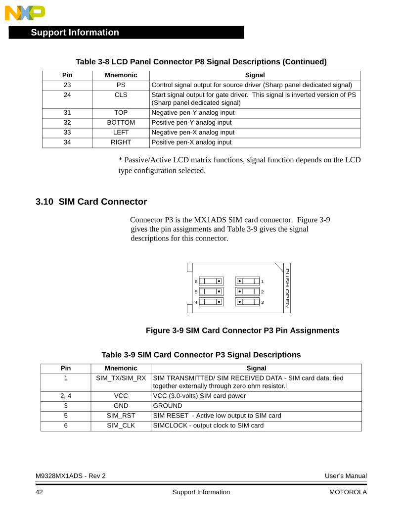
3.10 SIM Card Connector
Connector P3 is the MX1ADS SIM card connector. Figure 3-9 gives the pin assignments and Table 3-9 gives the signal descriptions for this connector.
Figure 3-9 SIM Card Connector P3 Pin Assignments
23 PS Control signal output for source driver (Sharp panel dedicated signal)
24 CLS Start signal output for gate driver. This signal is inverted version of PS (Sharp panel dedicated signal)
31 TOP Negative pen-Y analog input
32 BOTTOM Positive pen-Y analog input
33 LEFT Negative pen-X analog input
34 RIGHT Positive pen-X analog input
Table 3-8 LCD Panel Connector P8 Signal Descriptions (Continued)
Pin Mnemonic Signal
PU
SH
OP
EN
1
2
34
5
6
Table 3-9 SIM Card Connector P3 Signal Descriptions
Pin Mnemonic Signal
1 SIM_TX/SIM_RX SIM TRANSMITTED/ SIM RECEIVED DATA - SIM card data, tied together externally through zero ohm resistor.l
2, 4 VCC VCC (3.0-volts) SIM card power
3 GND GROUND
5 SIM_RST SIM RESET - Active low output to SIM card
6 SIM_CLK SIMCLOCK - output clock to SIM card
M9328MX1ADS - Rev 2 User’s Manual
42 Support Information MOTOROLA
Support InformationMemory Stick Connector
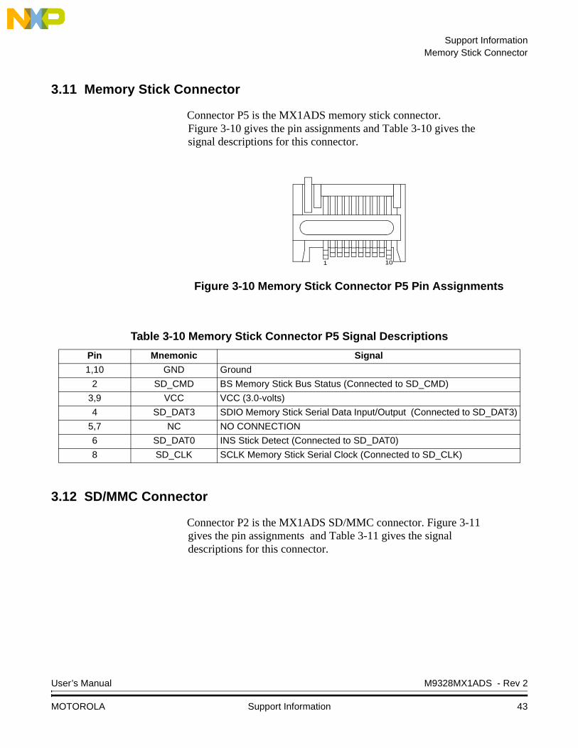
3.11 Memory Stick Connector
Connector P5 is the MX1ADS memory stick connector. Figure 3-10 gives the pin assignments and Table 3-10 gives the signal descriptions for this connector.
Figure 3-10 Memory Stick Connector P5 Pin Assignments
3.12 SD/MMC Connector
Connector P2 is the MX1ADS SD/MMC connector. Figure 3-11 gives the pin assignments and Table 3-11 gives the signal descriptions for this connector.
1 10
Table 3-10 Memory Stick Connector P5 Signal Descriptions
Pin Mnemonic Signal
1,10 GND Ground
2 SD_CMD BS Memory Stick Bus Status (Connected to SD_CMD)
3,9 VCC VCC (3.0-volts)
4 SD_DAT3 SDIO Memory Stick Serial Data Input/Output (Connected to SD_DAT3)
5,7 NC NO CONNECTION
6 SD_DAT0 INS Stick Detect (Connected to SD_DAT0)
8 SD_CLK SCLK Memory Stick Serial Clock (Connected to SD_CLK)
User’s Manual M9328MX1ADS - Rev 2
MOTOROLA Support Information 43

Support Information
Figure 3-11 SD/MMC Connector P2 Pin Assignments
Table 3-11 SD/MMC Connector P2 Signal Descriptions
Pin Mnemonic
Signal
MMC CardSD Card
1-Bit Mode 4-Bit Mode
1 SD_DAT3 Reserved Not Used Data Line DAT3
2 SD_CMD Command / Response
3 GND Ground
4 VCC Supply Voltage (3.0-volts)
5 SD_CLK Clock
6 GND Ground
7 SD_DAT0 Data Line DAT0
8 SD_DAT1 Not Used Interrupt (IRQ) Data Line DAT1 or Interrupt (IRQ)
9 SD_DAT2 Not Used ReadWait (RW) Data Line DAT2 or Read Wait (RW)
10 USBD_AFE Card Detect, configured as GPIO, PB20
11 GND Ground
16 SD_WP Write Protect Detect, connects to I/O Expander, U42-13 (P10)
12345678 91011 16
M9328MX1ADS - Rev 2 User’s Manual
44 Support Information MOTOROLA
Support InformationExpansion Connector
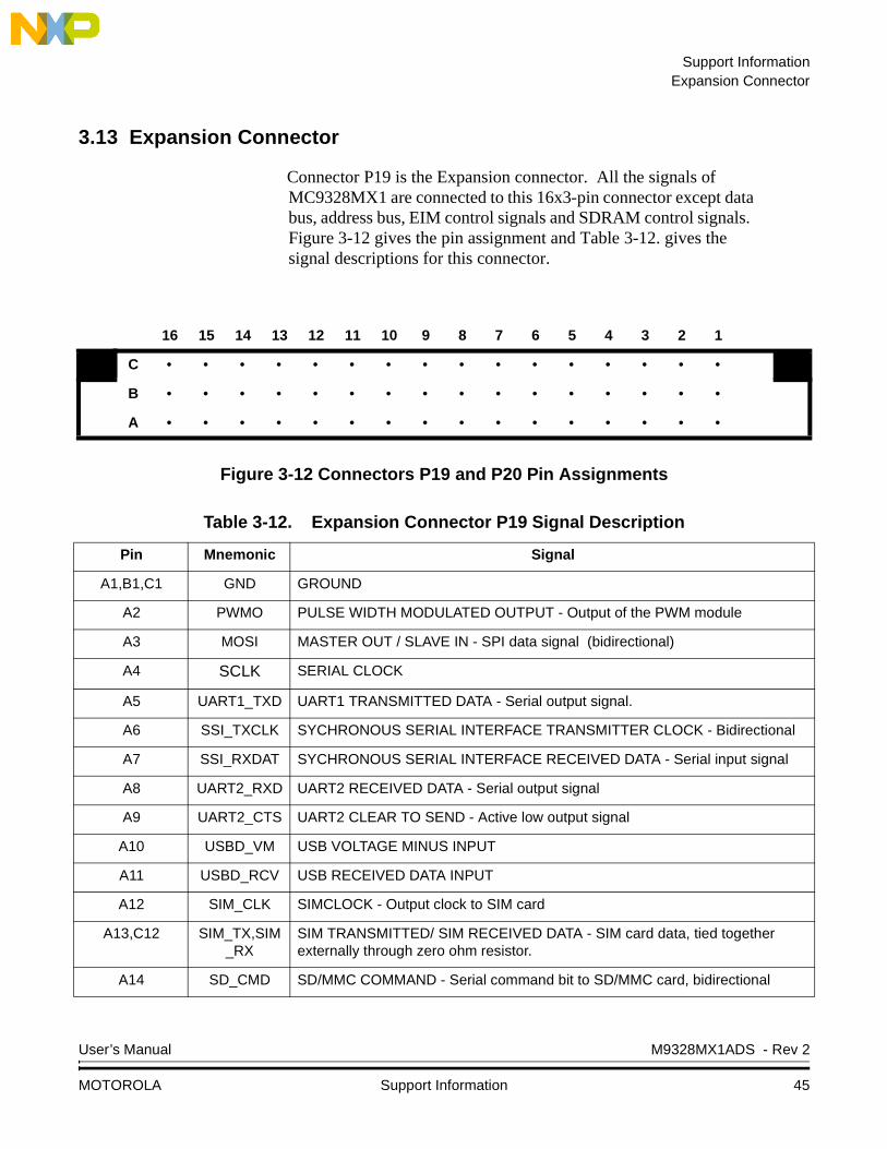
3.13 Expansion Connector
Connector P19 is the Expansion connector. All the signals of MC9328MX1 are connected to this 16x3-pin connector except data bus, address bus, EIM control signals and SDRAM control signals. Figure 3-12 gives the pin assignment and Table 3-12. gives the signal descriptions for this connector.
Figure 3-12 Connectors P19 and P20 Pin Assignments
16 15 14 13 12 11 10 9 8 7 6 5 4 3 2 1
C • • • • • • • • • • • • • • • •
B • • • • • • • • • • • • • • • •
A • • • • • • • • • • • • • • • •
Table 3-12. Expansion Connector P19 Signal Description
Pin Mnemonic Signal
A1,B1,C1 GND GROUND
A2 PWMO PULSE WIDTH MODULATED OUTPUT - Output of the PWM module
A3 MOSI MASTER OUT / SLAVE IN - SPI data signal (bidirectional)
A4 SCLK SERIAL CLOCK
A5 UART1_TXD UART1 TRANSMITTED DATA - Serial output signal.
A6 SSI_TXCLK SYCHRONOUS SERIAL INTERFACE TRANSMITTER CLOCK - Bidirectional
A7 SSI_RXDAT SYCHRONOUS SERIAL INTERFACE RECEIVED DATA - Serial input signal
A8 UART2_RXD UART2 RECEIVED DATA - Serial output signal
A9 UART2_CTS UART2 CLEAR TO SEND - Active low output signal
A10 USBD_VM USB VOLTAGE MINUS INPUT
A11 USBD_RCV USB RECEIVED DATA INPUT
A12 SIM_CLK SIMCLOCK - Output clock to SIM card
A13,C12 SIM_TX,SIM_RX
SIM TRANSMITTED/ SIM RECEIVED DATA - SIM card data, tied together externally through zero ohm resistor.
A14 SD_CMD SD/MMC COMMAND - Serial command bit to SD/MMC card, bidirectional
User’s Manual M9328MX1ADS - Rev 2
MOTOROLA Support Information 45

Support Information
A15 SD_DAT2 SD/MMC DATA BIT 2 - Serial data bit to SD/MMC card, bidirectional
A16,B16,C16 VCC VCC (3.0-volts)
B2 TIN TIMER INPUT CAPTURE - Timer input
B3 MISO MASTER IN / SLAVE OUT - SPI data signal (bidirectional
B4 SPI_RDY SPI READY - CSPI serial burst trigger, active low input
B5 UART1_RTS UART1 REQUEST TO SEND - Active low input signal
B6 SSI_TXFS SYCHRONOUS SERIAL INTERFACE TRANSMITTER FRAME SYNC
B7 SSI_RXCLK SYCHRONOUS SERIAL INTERFACE RECEIVER CLOCK - Bidirectional
B8 UART2_TXD UART2 TRANSMITTED DATA - Serial output signal
B9 USBD_VMO USB VOLTAGE MINUS OUPUT
B10 USBD_VP USB VOLTAGE POSITIVE INPUT
B11 USBD_ROE USB DATA RECEIVED OUTPUT ENABLE - Active low output
B12 SIM_RST SIM RESET - Active low output to SIM card
B13 SIM_PD SIM PRESENCE DETECT - Active low input
B14 SD_CLK SD/MMC CLOCK - Clock output to SD/MMC card
B15 SD_DAT1 SD/MMC DATA BIT 1 - Serial data bit to SD/MMC card, bidirectional
C2 TOUT12 TIMER OUTPUT COMPARE
C3 SS SLAVE SELECT - Bidirectional, active low, slave mode input, master mode output.
C4 UART1_RXD UART1 RECEIVED DATA - Serial output signal
C5 UART1_CTS UART1 CLEAR TO SEND - Active low output signal
C6 SSI_TXDAT SYCHRONOUS SERIAL INTERFACE TRANSMITTED DATA - Serial output signal
C7 SSI_RXFS SYCHRONOUS SERIAL INTERFACE RECEIVER FRAME SYNC - Bidirectional
C8 UART2_RTS UART2 REQUEST TO SEND - Active low input signal
C9 USBD_VPO USB VOLTAGE POSITIVE OUTPUT
C10 USBD_SUSPND
USB SUSPEND OUTPUT
C11 USBD_AFE USB ANALOG FRONT END ENABLE
C13 SIM_SVEN SIM VCC ENABLE - Enable power to the SIM card, active low
Table 3-12. Expansion Connector P19 Signal Description
M9328MX1ADS - Rev 2 User’s Manual
46 Support Information MOTOROLA

Support InformationImage Sensor Connector
3.14 Image Sensor Connector
P20 is a 16x3-pin connector P20 is assigned with signals for Image Sensor. Daughter card supporting different image sensor can plugged to this connec-tors. Figure 3-12 gives the pin assignment of this connector and Table 3-13. gives the signal descriptions for this connector.
C14 SD_DAT3 SD/MMC DATA BIT 3 - Serial data bit to SD/MMC card, bidirectional
C15 SD_DAT0 SD/MMC DATA BIT 0 - Serial data bit to SD/MMC card, bidirectional
Table 3-12. Expansion Connector P19 Signal Description
Table 3-13. Image Sensor Connector P20 Signal Description
Pin Mnemonic Signal
A1,B1,C1 GND GROUND
A2 CSI_D0 CMOS SENSOR INTERFACE DATA 0 - Data input from Image Sensor
A3 CSI_D2 CMOS SENSOR INTERFACE DATA 2- Data input from Image Sensor
A4 CSI_D4 CMOS SENSOR INTERFACE DATA 4- Data input from Image Sensor
A5 CSI_D6 CMOS SENSOR INTERFACE DATA 6- Data input from Image Sensor
A6 CSI_PIXCLK CMOS SENSOR INTERFACE PIXAL CLOCK - Data latch strobe
A7 CSI_VSYNC CMOS SENSOR INTERFACE VERTICAL SYNC - Control input
A8 I2C_CLK I SQUARED C CLOCK - Serial clock, bidirectional
A9 MOSI/PC17 MASTER OUT / SLAVE IN or PORT C BIT 17 - Not used by CSI daughter card
A10 ~CS4/PA22 CHIP SELECT 4 / PORT A BIT 23 - Not used by CSI daughter card
A11-A15 NC NO CONNECTION
A16,B16,C16 VCC VCC (3.0-volts)
B2-B15 NC NO CONNECTION
C2 CSI_D1 CMOS SENSOR INTERFACE DATA 1- Data input from Image Sensor
C3 CSI_D3 CMOS SENSOR INTERFACE DATA 3- Data input from Image Sensor
C4 CSI_D5 CMOS SENSOR INTERFACE DATA 5 - Data input from Image Sensor
C5 CSI_D7 CMOS SENSOR INTERFACE DATA 7 - Data input from Image Sensor
C6 CSI_HSYNC CMOS SENSOR INTERFACE HORIZONTAL SYNC- Active low input
User’s Manual M9328MX1ADS - Rev 2
MOTOROLA Support Information 47

Support Information
C7 CSI_MCLK CMOS SENSOR INTERFACE MASTER CLOCK - Clock output to sensor card
C8 I2C_DAT I SQUARED C DATA - Serial data, bidirectional
C9 TIN/PA1 TIMER INPUT CAPTURE/ PORT A BIT 1 - - Not used by CSI daughter card
C10 ~CS5/PA23 CHIP SELECT 5 / PORT A BIT 23 - Configured for GPIO to act as a SYNC signal
C11 SIM_RST SIM RESET - Configured as GPIO for Image sensor’s Unit signal.
C12 SIM_CLK SIM CLOCK -
C13-C15 NC NO CONNECTION
Table 3-13. Image Sensor Connector P20 Signal Description
M9328MX1ADS - Rev 2 User’s Manual
48 Support Information MOTOROLA


HOW TO REACH US:
World Wide Web Address
Motorola: http://www.motorola.com/General/index.html
Information in this document is provided solely to enable system and software
implementers to use Motorola products. There are no express or implied copyright
licenses granted hereunder to design or fabricate any integrated circuits or
integrated circuits based on the information in this document.
Motorola reserves the right to make changes without further notice to any products
herein. Motorola makes no warranty, representation or guarantee regarding the
suitability of its products for any particular purpose, nor does Motorola assume any
liability arising out of the application or use of any product or circuit, and specifically
disclaims any and all liability, including without limitation consequential or incidental
damages. “Typical” parameters which may be provided in Motorola data sheets
and/or specifications can and do vary in different applications and actual
performance may vary over time. All operating parameters, including “Typicals”
must be validated for each customer application by customer’s technical experts.
Motorola does not convey any license under its patent rights nor the rights of
others. Motorola products are not designed, intended, or authorized for use as
components in systems intended for surgical implant into the body, or other
applications intended to support or sustain life, or for any other application in which
the failure of the Motorola product could create a situation where personal injury or
death may occur. Should Buyer purchase or use Motorola products for any such
unintended or unauthorized application, Buyer shall indemnify and hold Motorola
and its officers, employees, subsidiaries, affiliates, and distributors harmless
against all claims, costs, damages, and expenses, and reasonable attorney fees
arising out of, directly or indirectly, any claim of personal injury or death associated
with such unintended or unauthorized use, even if such claim alleges that Motorola
was negligent regarding the design or manufacture of the part.
Motorola and the Stylized M Logo are registered in the U.S. Patent and Trademark Office. digital dna is a trademark of Motorola, Inc. All other product or service names are the property of their respective owners. Motorola, Inc. is an Equal Opportunity/Affirmative Action Employer.
© Motorola, Inc. 2002
M9328MX1ADSUM/D