Embed Size (px)
Citation preview
13
Appendix II. SOP for Nano Imprint Lithography Patterned Si Wafers
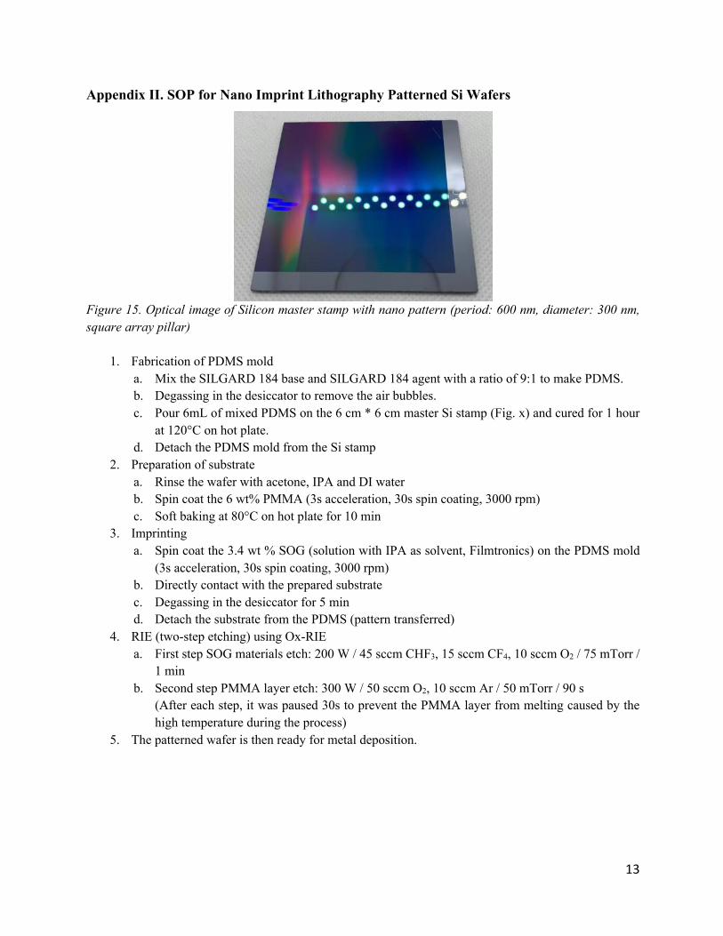
Figure 15. Optical image of Silicon master stamp with nano pattern (period: 600 nm, diameter: 300 nm, square array pillar)
1. Fabrication of PDMS mold a. Mix the SILGARD 184 base and SILGARD 184 agent with a ratio of 9:1 to make PDMS. b. Degassing in the desiccator to remove the air bubbles. c. Pour 6mL of mixed PDMS on the 6 cm * 6 cm master Si stamp (Fig. x) and cured for 1 hour
at 120°C on hot plate. d. Detach the PDMS mold from the Si stamp
2. Preparation of substrate a. Rinse the wafer with acetone, IPA and DI water b. Spin coat the 6 wt% PMMA (3s acceleration, 30s spin coating, 3000 rpm) c. Soft baking at 80°C on hot plate for 10 min
3. Imprinting a. Spin coat the 3.4 wt % SOG (solution with IPA as solvent, Filmtronics) on the PDMS mold
(3s acceleration, 30s spin coating, 3000 rpm) b. Directly contact with the prepared substrate c. Degassing in the desiccator for 5 min d. Detach the substrate from the PDMS (pattern transferred)
4. RIE (two-step etching) using Ox-RIE a. First step SOG materials etch: 200 W / 45 sccm CHF3, 15 sccm CF4, 10 sccm O2 / 75 mTorr /
1 min b. Second step PMMA layer etch: 300 W / 50 sccm O2, 10 sccm Ar / 50 mTorr / 90 s
(After each step, it was paused 30s to prevent the PMMA layer from melting caused by the high temperature during the process)
5. The patterned wafer is then ready for metal deposition.