Embed Size (px)
Citation preview
Subnanometer Replica Molding of MolecularSteps on Ionic CrystalsSelim Elhadj,†,| Robert M. Rioux,‡,| Michael D. Dickey,‡ James J. DeYoreo,*,§ andGeorge M. Whitesides*,‡
†Physical and Life Sciences Directorate, Lawrence Livermore National Laboratory, 7000 East Avenue, Livermore,California 94550, ‡Department of Chemistry and Chemical Biology, Harvard University, 12 Oxford Street,Cambridge, Massachusetts 02138, and §The Molecular Foundry, Materials Science Division, Lawrence BerkeleyNational Laboratory, 1 Cyclotron Road, Berkeley, California 94720
ABSTRACT Replica molding with elastomeric polymers has been used routinely to replicate features less than 10 nm in size. Becausethe theoretical limit of this technique is set by polymer-surface interactions, atomic radii, and accessible volumes, replication atsubnanometer length scales should be possible. Using polydimethylsiloxane to create a mold and polyurethane to form the replica,we demonstrate replication of elementary steps 3-5 Å in height that define the minimum separation between molecular layers inthe lattices of the ionic crystals potassium dihydrogen phosphate and calcite. This work establishes the operation of replica moldingat the molecular scale.
KEYWORDS Replica molding, KDP, calcite, molecular scale, PDMS, imprint lithography
Replication of features above 10 nm by replica mold-ingusingelastomericpolymershasbecomeroutine.1,2
Replication of sub-10 nm features is still a significantchallenge because at this length-scale the feature size ap-proaches that of the monomers used for replication. Thetheoretical limits to replica molding are set by the granularityof matter and by the intermolecular interactions that deter-mine the ability of molecular surfaces to come into confor-mal contact.3 In particular, whether a polymer can take onthe curvature required to conform to molecular-scale varia-tions in topography should depend on the interfacial energyof the polymer-surface contact. While there are some ex-amples of replication below 10 nm,4-8 replication of mo-lecular-scale features has not been achieved. Here we takeadvantage of the regular arrays of single molecular-heightsteps on the faces of ionic crystals to demonstrate that thevery low interfacial free energy, flexibility, and resistanceto contamination of h-PDMS (hard-polydimethylsiloxane)enables replica molding with subnanometer resolution.
Replica molding is the transfer of a topographical patternfrom a “master” substrate into a polymer or other materialto form the inverse mold, and the subsequent fabrication ofa replica by solidifying a liquid precursor against the inversemold.2 Because of its ease of application to a wide varietyof materials, replica molding has been pursued as a generalapproach to repeatable production of nanostructured sur-faces starting from a single, high-precision master.1,2 Suc-
cessful replication of features below 10 nm using elastomericpolymers, such as PDMS has been demonstrated for anumber of materials.4-9 The lower limit on the size offeatures to which replica molding can be applied is, however,ultimately determined by atomic radii, molecular shapes,van der Waals interactions, and thermal and entropic ef-fects3 and remains largely unexplored. Because the stepheights of ionic crystals are smaller than both the monomersand the radius of gyration of the elastomeric polymers usedfor replication, prior to this study it was not obvious whetherthe molding process would be capable of replicating theatomic steps of the crystal surface. However, to aid invisualizing how large polymer molecules might replicatemuch smaller features the polymers can be thought of asspherical or ellipsoidal particles bunched around a smallstep. As long as their spatial configuration is maintained afterremoval of the step, they will have replicated the underlyingstep structure albeit with a distortion related to their specificsize and interactions.
Thus, successful investigation in this lower limit requiressurfaces with regular, well-defined features at the molecularscale. Ionic crystal surfaces present elementary steps withtypical heights of ∼0.3-0.8 nm, which provide a convenientand reproducible master with molecular-sized features thatcan be used to assess the performance of replica moldingat this scale. The angstrom scale architectures achieved bythe replication in this study can be significant to the nano-technology industry seeking more stringent, scalable nano-fabrication methods because they show that new limits onthe feature size accessible through stamp-based techniquescan now be pursued. This work has implications for imprintlithography techniques, which are now on the semiconduc-tor roadmap due to their ability to pattern high-resolution
* To whom correspondence should be addressed. E-mail: (G.M.W) [email protected]; (J.J.D) [email protected].| These authors contributed equally to this work.Received for review: 07/11/2010Published on Web: 09/15/2010
pubs.acs.org/NanoLett
© 2010 American Chemical Society 4140 DOI: 10.1021/nl102409d | Nano Lett. 2010, 10, 4140–4145
features at a significantly lower cost than next-generationphotolithographic processes.
In this study, we implemented siloxane formulations thathave been optimized previously for high-resolution moldingbased on their viscosity, modulus, and surface hardness(refer to the Supporting Information for experimental de-tails).10 The composite structure for replica molding com-prising a thin (<100 µm) h-PDMS10 film formed in directcontact with single crystal surfaces and backed by a signifi-cantly thicker (∼3 mm) layer of “normal”-PDMS (n-PDMS).This design was chosen for three reasons. First, the largeelastic modulus (∼9 N mm-2) of h-PDMS10 allowed replica-tion of shallow relief features with higher fidelity than ispossible using n-PDMS; the high compressibility of n-PDMSoften leads to deformation, buckling, or collapse of sub-100nm features formed on its surface.11 Second, the very lowinterfacial free energy of h-PDMS and the flexibility of thecomposite structure enables replication without any priormodification to the crystal or polymer surfaces.11 Third,h-PDMS is inert to ambient air, particles, and vapors; thislack of contamination reduces adhesion to both the crystaland the polyurethane (PU) replica formed from it and thuseases release during replication.
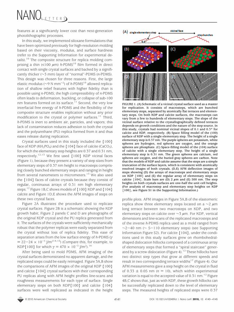
Crystal surfaces used in this study included the {100}face of KDP (KH2PO4) and the {104} face of calcite (CaCO3),for which the elementary step heights are 0.37 and 0.31 nm,respectively.12,13 We first used {100} KDP vicinal faces(Figure 1), because they present a variety of step sizes fromelementary steps of 0.37 nm height to macrosteps compris-ing closely bunched elementary steps and ranging in heightfrom several nanometers to micrometers.13 We also usedthe {104} faces of calcite crystals because they consist ofregular, continuous arrays of 0.31 nm high elementarysteps.12 Figure 1B,C shows models of {100} KDP and {104}calcite and Figure 1D,E shows the AFM images of steps onthese two crystal faces.
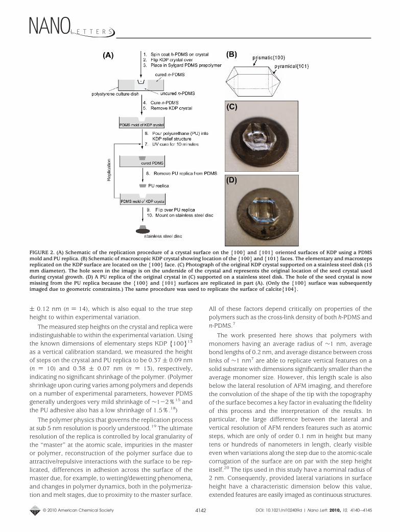
Figure 2A illustrates the procedure used to replicatecrystal surfaces. Figure 2B is a schematic showing the KDPgrowth habit; Figure 2 panels C and D are photographs ofthe original KDP crystal and the PU replica generated fromit. The surfaces of the crystals were sufficiently mechanicallyrobust that the polymer replicas were easily separated fromthe crystal without loss of replica fidelity. This ease ofseparation arises from the low surface energy of h-PDMS (γ) 22-24 × 10-3 J/m214,15) (Compare this, for example, toKDP{100} for which γ ) 470 × 10-3 J/m2).16
After being used to mold PDMS, AFM imaging of thecrystal surfaces demonstrated no apparent damage, and thereplicated steps could be easily reimaged. Figure 3A,B showthe comparisons of AFM images of the original KDP {100}and calcite {104} crystal surfaces with their correspondingPU replicas along with AFM height profiles line-scans androughness measurements for each type of surface. Singleelementary steps on both KDP{100} and calcite {104}surfaces were well replicated as indicated in the height
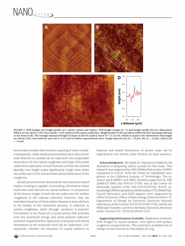
profile plots. AFM images in Figure 3A,B of the elastomericreplica show three elementary steps located on a ∼2 µmlong terrace between two macrosteps on KDP, and twoelementary steps on calcite over ∼3 µm. For KDP, verticaldimensions and line-scans of the replicated macrosteps andof the inverse h-PDMS replica used as a mold ranged from∼2-40 nm (∼ 5-110 elementary steps) (see SupportingInformation Figure S2). For calcite {104}, under the condi-tions used in this study surfaces grew on rhombohedral-shaped dislocation hillocks composed of a continuous arrayof elementary steps that formed a “spiral staircase” gener-ated by a screw dislocation (Figure 4).12 These hillocks havetwo distinct step types that grow at different speeds andresult in two corresponding terrace widths17 (Figure 4). OurAFM measurements gave a step height on the crystal in fluidof 0.33 ( 0.05 nm (n ) 10), which within experimentalvariation is equal to the accepted value of 0.31 nm.12 Figure4B,C shows that, just as with KDP, these growth hillocks canbe successfully replicated down to the level of elementarysteps. The measured heights of replicated steps were 0.37
FIGURE 1. (A) Schematic of a vicinal crystal surface used as a masterfor replication. It consists of macrosteps, which are bunchedelementary steps, separated by atomically flat terraces and elemen-tary steps. On both KDP and calcite surfaces, the macrosteps canvary from a few to hundreds of elementary steps. The slope of thevicinal surface relative to the crystallographically defined terracesdepends on growth conditions and the nature of the step source. Inthis study, crystals had nominal vicinal slopes of 0.1 and 0.3° forcalcite and KDP, respectively. (B) Space filling model of the (100)surface of KDP with a single elementary step. The height of a singleelementary step is 0.37 nm. The purple spheres are potassium, whitespheres are hydrogen, red spheres are oxygen, and the orangespheres are phosphate. (C) Space-filling model of the (104) surfaceof calcite with a single elementary step. The height of a singleelementary step is 0.31 nm. The green spheres are calcium, redspheres are oxygen, and the buried gray spheres are carbon. Notethat the models of KDP and calcite assume that the steps are a simpletruncation of the surface layers, which is consistent with atomicallyresolved images of both crystals. (D,E) AFM deflection images ofsteps showing (D) the arrays of macrosteps and elementary stepson KDP {100} and (E) the regular array of elementary steps oncalcite {104}. Scale bars are (D) 2 µm and (E) 500 nm. The stepheights on both crystals surfaces are one-half the unit cell heights.(For analysis of macrostep and elementary step heights on KDP{100}, see Figure S1 in the Supporting Information.)
© 2010 American Chemical Society 4141 DOI: 10.1021/nl102409d | Nano Lett. 2010, 10, 4140-–4145
( 0.12 nm (n ) 14), which is also equal to the true stepheight to within experimental variation.
The measured step heights on the crystal and replica wereindistinguishable to within the experimental variation. Usingthe known dimensions of elementary steps KDP {100}13
as a vertical calibration standard, we measured the heightof steps on the crystal and PU replica to be 0.37 ( 0.09 nm(n ) 10) and 0.38 ( 0.07 nm (n ) 13), respectively,indicating no significant shrinkage of the polymer. (Polymershrinkage upon curing varies among polymers and dependson a number of experimental parameters, however PDMSgenerally undergoes very mild shrinkage of ∼1-2%15 andthe PU adhesive also has a low shrinkage of 1.5%.18)
The polymer physics that governs the replication processat sub 5 nm resolution is poorly understood.19 The ultimateresolution of the replica is controlled by local granularity ofthe “master” at the atomic scale, impurities in the masteror polymer, reconstruction of the polymer surface due toattractive/repulsive interactions with the surface to be rep-licated, differences in adhesion across the surface of themaster due, for example, to wetting/dewetting phenomena,and changes in polymer dynamics, both in the polymeriza-tion and melt stages, due to proximity to the master surface.
All of these factors depend critically on properties of thepolymers such as the cross-link density of both h-PDMS andn-PDMS.7
The work presented here shows that polymers withmonomers having an average radius of ∼1 nm, averagebond lengths of 0.2 nm, and average distance between crosslinks of ∼1 nm7 are able to replicate vertical features on asolid substrate with dimensions significantly smaller than theaverage monomer size. However, this length scale is alsobelow the lateral resolution of AFM imaging, and thereforethe convolution of the shape of the tip with the topographyof the surface becomes a key factor in evaluating the fidelityof this process and the interpretation of the results. Inparticular, the large difference between the lateral andvertical resolution of AFM renders features such as atomicsteps, which are only of order 0.1 nm in height but manytens or hundreds of nanometers in length, clearly visibleeven when variations along the step due to the atomic-scalecorrugation of the surface are on par with the step heightitself.20 The tips used in this study have a nominal radius of2 nm. Consequently, provided lateral variations in surfaceheight have a characteristic dimension below this value,extended features are easily imaged as continuous structures.
FIGURE 2. (A) Schematic of the replication procedure of a crystal surface on the {100} and {101} oriented surfaces of KDP using a PDMSmold and PU replica. (B) Schematic of macroscopic KDP crystal showing location of the {100} and {101} faces. The elementary and macrostepsreplicated on the KDP surface are located on the {100} face. (C) Photograph of the original KDP crystal supported on a stainless steel disk (15mm diameter). The hole seen in the image is on the underside of the crystal and represents the original location of the seed crystal usedduring crystal growth. (D) A PU replica of the original crystal in (C) supported on a stainless steel disk. The hole of the seed crystal is nowmissing from the PU replica because the {100} and {101} surfaces are replicated in part (A). (Only the {100} surface was subsequentlyimaged due to geometric constraints.) The same procedure was used to replicate the surface of calcite{104}.
© 2010 American Chemical Society 4142 DOI: 10.1021/nl102409d | Nano Lett. 2010, 10, 4140-–4145
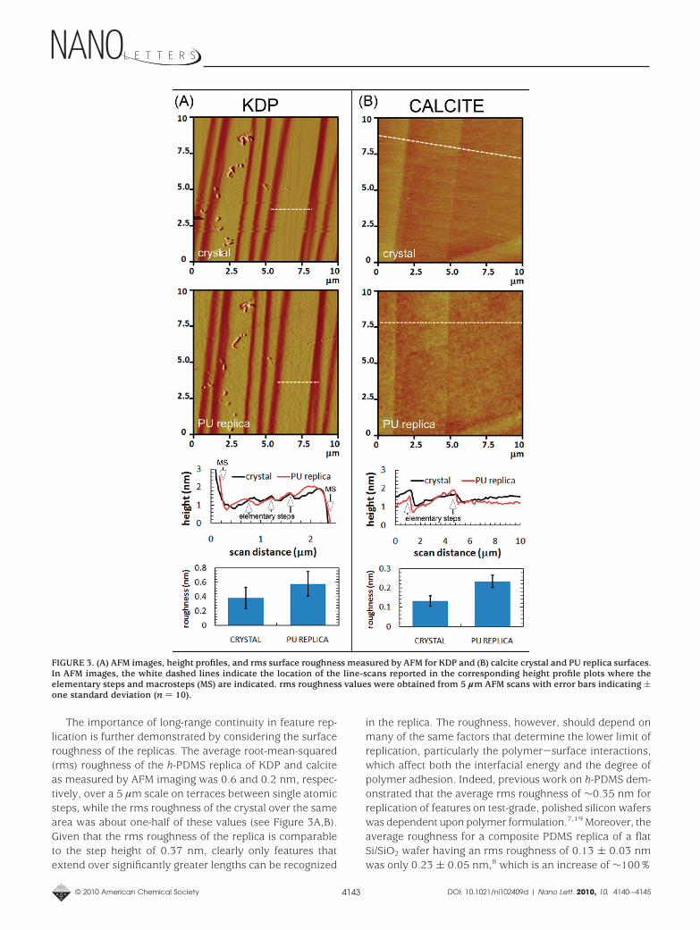
The importance of long-range continuity in feature rep-lication is further demonstrated by considering the surfaceroughness of the replicas. The average root-mean-squared(rms) roughness of the h-PDMS replica of KDP and calciteas measured by AFM imaging was 0.6 and 0.2 nm, respec-tively, over a 5 µm scale on terraces between single atomicsteps, while the rms roughness of the crystal over the samearea was about one-half of these values (see Figure 3A,B).Given that the rms roughness of the replica is comparableto the step height of 0.37 nm, clearly only features thatextend over significantly greater lengths can be recognized
in the replica. The roughness, however, should depend onmany of the same factors that determine the lower limit ofreplication, particularly the polymer-surface interactions,which affect both the interfacial energy and the degree ofpolymer adhesion. Indeed, previous work on h-PDMS dem-onstrated that the average rms roughness of ∼0.35 nm forreplication of features on test-grade, polished silicon waferswas dependent upon polymer formulation.7,19 Moreover, theaverage roughness for a composite PDMS replica of a flatSi/SiO2 wafer having an rms roughness of 0.13 ( 0.03 nmwas only 0.23 ( 0.05 nm,8 which is an increase of ∼100%
FIGURE 3. (A) AFM images, height profiles, and rms surface roughness measured by AFM for KDP and (B) calcite crystal and PU replica surfaces.In AFM images, the white dashed lines indicate the location of the line-scans reported in the corresponding height profile plots where theelementary steps and macrosteps (MS) are indicated. rms roughness values were obtained from 5 µm AFM scans with error bars indicating (one standard deviation (n ) 10).
© 2010 American Chemical Society 4143 DOI: 10.1021/nl102409d | Nano Lett. 2010, 10, 4140-–4145
but remains smaller than the lattice spacing of most crystals.Consequently, while results presented here show that atomicscale features on crystals can be replicated, the comparabledimensions of rms replica roughness and large AFM proberadius limit replication of such features to those that extendlaterally over length scales significantly longer than eitherthe probe size or the characteristic lateral dimension of theroughness.
Results presented here demonstrate that elastomer-basedreplica molding is capable of providing information aboutmolecular-scale features on crystal surfaces. A comparisonof the feature height to both the tip radius and the surfaceroughness of the replicas indicated, however, that theextended character of these surface features is a key elementin the fidelity of the replication process. A reduction insurface roughness, either through variations in polymerformulation or by choice of a crystal surface that providesboth low interfacial energy and weak polymer adhesionwould be required before replication of features with lateraldimensions at the molecular level can be addressed. Con-sequently, whether the structure of crystal surfaces or
features with lateral dimensions of atomic scale can bereplicated at true atomic scale remains an open question.
Acknowledgment. We thank Dr. Raymond Friddle for hisassistance in preparing calcite crystals for this study. Thisresearch was supported by NIH (GM065364) and by DARPA(subaward to G.M.W. from the Center for Optofluidic Inte-gration at the California Institute of Technology). The re-search used MRSEC and NSEC facilities supported by NSF(DMR-0213805 and PHY-0117795) and at the Center forNanoscale Systems (CNS: NSE ECS-0335765). R.M.R. ac-knowledgesNIHforapostdoctoralfellowship(1F32NS060356).Crystal fabrication and AFM analysis were supported byOffice of Science, Office of Basic Energy Sciences of the U.S.Department of Energy by Lawrence Livermore NationalLaboratory under Contract DE-AC52-07NA27344, and by theMolecular Foundry, Lawrence Berkeley National Laboratoryunder Contract No. DE-AC02-05CH11231.
Supporting Information Available. Replication methods,AFM images of crystal surfaces, and replica with surfaceroughness measurements. This material is available free ofcharge via the Internet at http://pubs.acs.org.
FIGURE 4. AFM images and height profile of a calcite crystal and replica. AFM height images (A-C) and height profile (D) of a dislocationhillock on (A) calcite {104} face and (B-C) PU replica of the same crystal face. Height profile in (D) was taken within the box and perpendicularto the lines in (B). The average measured height of steps on the PU replica was 0.37 ( 0.12 nm, which is equal to the elementary step heighton calcite{104} (one-half the unit cell or 0.31 nm) to within experimental error. Image sizes are (A) 10 × 10 µm, (B) 12 × 12 µm, and (C) 20× 14 µm.
© 2010 American Chemical Society 4144 DOI: 10.1021/nl102409d | Nano Lett. 2010, 10, 4140-–4145
REFERENCES AND NOTES(1) Gates, B. D.; Xu, Q. B.; Love, J. C.; Wolfe, D. B.; Whitesides, G. M.
Annu. Rev. Mater. Res. 2004, 34, 339–372.(2) Gates, B. D.; Xu, Q. B.; Stewart, M.; Ryan, D.; Willson, C. G.;
Whitesides, G. M. Chem. Rev. 2005, 105 (4), 1171–1196.(3) The ultimate practical limit to replica molding has not been
established. It should be below that accessible by photolithogra-phy and is thus relevant to future nanomanufacturing. It may alsobe relevant to a number of areas of molecular chemistry .
(4) Deng, Z. X.; Mao, C. D. Angew. Chem., Int. Ed. 2004, 43 (31),4068–4070.
(5) Gabai, R.; Ismach, A.; Joselevich, E. Adv. Mater. 2007, 19 (10),1325–1330.
(6) Gates, B. D.; Whitesides, G. M. J. Am. Chem. Soc. 2003, 125 (49),14986–14987.
(7) Hua, F.; Sun, Y. G.; Gaur, A.; Meitl, M. A.; Bilhaut, L.; Rotkina, L.;Wang, J. F.; Geil, P.; Shim, M.; Rogers, J. A.; Shim, A. Nano Lett.2004, 4 (12), 2467–2471.
(8) Xu, Q. B.; Mayers, B. T.; Lahav, M.; Vezenov, D. V.; Whitesides,G. M. J. Am. Chem. Soc. 2005, 127 (3), 854–855.
(9) Lin, R. S.; Rogers, J. A. Nano Lett. 2007, 7 (6), 1613–1621.(10) Schmid, H.; Michel, B. Macromolecules 2000, 33 (8), 3042–3049.
(11) Odom, T. W.; Love, J. C.; Wolfe, D. B.; Paul, K. E.; Whitesides,G. M. Langmuir 2002, 18 (13), 5314–5320.
(12) Teng, H. H.; Dove, P. M.; Orme, C. A.; De Yoreo, J. J. Science 1998,282 (5389), 724–727.
(13) Thomas, T. N.; Land, T. A.; Martin, T.; Casey, W. H.; DeYoreo,J. J. J. Cryst. Growth 2004, 260 (3-4), 566–579.
(14) Chaudhury, M. K.; Whitesides, G. M. Langmuir 1991, 7 (5), 1013–1025.
(15) Choi, K. M.; Rogers, J. A. J. Am. Chem. Soc. 2003, 125 (14), 4060–4061.
(16) Stack, A. G.; Rustad, J. R.; DeYoreo, J. J.; Land, T. A.; Casey, W. H.J. Phys. Chem. B 2004, 108 (47), 18284–18290.
(17) Teng, H. H.; Dove, P. M.; DeYoreo, J. J. Geochim. Cosmo. Acta1999, 63 (17), 2507–2512.
(18) http://www.norlandprod.com/ (accessed July 20, 2010).(19) Hua, F.; Gaur, A.; Sun, Y. G.; Word, M.; Jin, N.; Adesida, I.; Shim,
M.; Shim, A.; Rogers, J. A. IEEE Trans. Nanotechnol. 2006, 5 (3),301–308.
(20) Friddle, R. W.; Weaver, M. L.; Qiu, S. R.; Wierzbicki, A.; Casey,W. H.; De Yoreo, J. J. Proc. Natl. Acad. Sci. U.S.A. 2010, 107 (1),11–15.
© 2010 American Chemical Society 4145 DOI: 10.1021/nl102409d | Nano Lett. 2010, 10, 4140-–4145