Embed Size (px)
Citation preview
Anti-counterfeit Integrated Circuits Using Fuse andTamper-Resistant Time-stamp Circuitry
Avinash R. Desai, Dinesh Ganta, Michael S. Hsiao, Leyla Nazhandali, Chao Wang, and Simin HallDepartment of Electrical and Computer Engineering, Virginia Tech,
Blacksburg VA 24061, USAEmail: {aviraj, diganta, mhsiao}@vt.edu
Abstract—Counterfeit Integrated Circuits (ICs) have becomean important security issue in recent years, in which counterfeitICs that perform incorrectly or sub-par to the expected canlead to catastrophic consequences in safety and/or mission-criticalapplications, in addition to the tremendous economic toll theyincur to the semiconductor industry. In this paper, we proposetwo novel methods to validate the authenticity of ICs. First, afuse with a charge pump is proposed to serve as a “seal” forthe IC, in which any functional use will break the seal, andthe broken seal is extremely hard to replace. Second, a noveltime-stamp is proposed that can provide the date at which theIC was manufactured. The time-stamp circuitry is constructedusing a Linear-Feedback Shift-Register (LFSR) such that anysmall change to the circuit would result in an entirely differentdate either in a distant past or future, beyond the lifetime of atypical IC. Furthermore, we propose a second layer of tamperresistance to the time-stamp circuit to make it even more difficultto modify. Results show that with about 8.8% area overhead inAES implementation, the adversary requires more than 10118
different trials to successfully tamper time-stamp circuit. Thesetechniques are easy to implement and embed into the circuit usingtodays technologies, while extremely difficult to modify or tamperwith by the adversary. Finally, the method can be combined withadditional hardware to detect malicious alteration made in thecircuit.
I. INTRODUCTION
In recent years, the horizontal semiconductor businessmodel has proven to be more beneficial and profitable to thesemiconductor industry as it improved both the cost and time-to-market. With globalization, a device can be manufacturedfrom practically any part of the world. However, in such amodel, a chip that resembles another visually may be used byan adversary as a counterfeit device. Not only will this incurtremendous financial loss to the leading-edge design houses,but they also pose severe security concerns. If the device isnot genuine, it may have incorrect or sub-par performancesuch that it may fail a system in the most critical moment ofthe operation. For critical applications used in medical, power-grid, and defense, trust remains to be of utmost priority. In fact,one major concern raised in a White House report on NationalStrategies for Smart Grid, Cybersecurity and Supply Chain2009 [2] was the lack of broadly applicable tools, techniques,and processes to detect or defeat counterfeiting and tamperingin the supply chain or deployed systems. The report empha-sizes on research needed in technology solutions to detect andprevent counterfeiting and overproduction. In another report,“we do not want a $12 million missile defense interceptor’sreliability compromised by a $2 counterfeit part,” indicated byGeneral O’Reilly Director, Missile Defense Agency [3].
Most of the high-end defense products have a huge numberof ICs in the system. For example, the U.S.’s next generationmulti-role fighter contains more than 3,500 ICs [3]. Compro-mising the trustworthiness of a single chip could result in acatastrophe. On the other hand, instances of counterfeits havebeen rising alarmingly. Another report by U.S. Department ofCommerce [4] brings to light that the number of counterfeitincidents in the defense supply chain has increased drasticallyfrom 3,868 in 2005 to 9,356 in 2008. Financially, counterfeitICs have a serious impact on revenue generated by a particulardesign house. The Semiconductor Industry Association (SIA)estimates that counterfeits cost U.S semiconductor companiesmore than $7.5 billion annually in lost revenue, a figure SIAsays results in loss of nearly 11,000 American jobs [3].
Considering all the above, it is extremely important to beable to determine if an IC is authentic and filter out all thecounterfeit parts. To determine this, one needs to answer twoquestions as illustrated in Figure 1: first, whether the IC isnew or used; second, the batch information when the IC wasmanufactured, for example, the date of manufacturing.
Unknown
IC under
counterfeit
test
New/Used Age
Aspect 1 Aspect 2
Fig. 1: Two Aspects for Counterfeit detection
While many existing techniques today, such as watermark-ing, metering and PUF (Physically Unclonable Function) basedtechniques, can be used as a mechanism to tackle against coun-terfeiting, they all require a substantial modification to eitherthe original design or the registration process. In addition,the identification of authentic and counterfeit ICs would be atedious process using such techniques. For example, one wouldneed to query a database of PUF challenge-response pairs todetermine if the the response matches the registered value.Likewise, revealing the watermark embedded in the design canbe a costly process. An ideal counterfeit detection techniquewould be one in which there is an universal standard to provethe authenticity of IC. Furthermore, with this standard, onewould prefer that the designer should not have to make largemodification in the design to make the chips compliant.
Our strategic goal is to provide a universal standard todetect counterfeit ICs with the help of two novel methodologies
978-1-4799-1535-4/13/$31.00 ©2013 IEEE 480
which can offer protection against counterfeits and yet beeasily implemented:
1) We introduce a fuse with a charge pump method to tacklethe first problem to distinguish between new and used ICs.In this technique, a fuse is used as a seal which breaksonly on functional use of the device.
2) Second, we present a LFSR-based time-stamp circuitwhich gives out the date the IC is manufactured witha query. The query is a sequence of input vectors toretrieve the manufactured date. The time-stamp circuitis embedded in the circuit such that it is extremelydifficult to make it return a date that differs from theoriginal time-stamp even just slightly. We also add anadditional layer of tamper-resistance guard against moresophisticated attacks to the time-stamp circuit.
Both of the two techniques are easily implementable andconsumes a small fraction of the chip real-estate. Our resultsindicate an average area overhead of 0.74% in implementingonly the time-stamp circuit.
The rest of the paper is organized as follows. Section 2presents the related work done in counterfeit detection andmotivation for work. Section 3 describes fuse and basic time-stamp methodology. Section 4 explains an obfuscated hardwarebased approach for tamper resistant time-stamp. Section 5describes additional implementation details. Section 6 presentsthe experimental results. Section 7 concludes the paper anddiscusses directions for future work.
II. RELATED WORK
Traditional techniques such as printing serial numbers orbarcodes to prevent counterfeiting of ICs in integrated circuitsare ineffective as they offer very weak resistance to attacks andcan be easily cloned or faked. There have been much effort inthe past to protect IP theft and cloning of ICs. Watermarking[5], [6], [7] have been used for detecting a class of counterfeitsas there are certain characteristics and properties in the circuitwhich help the user to prove the copyrights of the design.These watermarks often need to be changed with each designfor proper identification leading to a high design overhead. Inaddition, checking for the correct watermark for each devicefrom the vendor may require millions of instructions perdevice, making it both infeasible and impractical.
Most of the metering techniques [9], [10], [11], [12] usePUFs to produce locked ICs. Each and every IC has a differentinput sequence to unlock it in order to bring it to functionaluse. This helps the design house to maintain a database of ICsmanufactured and their respective ages. However, keeping adatabase of all the ICs adds up a huge overhead in IC lifespanand may be infeasible. PUF-based implementation [13] and useof stressed ring oscillators [8] are also methods to estimate ageof ICs. Nevertheless, the measuring of the age also requires achallenge-response database lookup which is cumbersome andtime-consuming.
All the above techniques lack a simple, yet effectivemethod to determine if a chip has been used and/or give outthe manufactured date for the IC in question. Furthermore, anon-trivial amount of changes are required to implement theprevious methods. In this work, we aim to provide a simple
and efficient way for ICs such that counterfeit chips are easilydetectable.
A. Reverse Engineering
Reverse engineering is the process through which adversaryobtain details of the circuit for a given IC. Adversary takesadvantages of tools and techniques specifically designed for theintended purpose. Techniques used in reverse engineering canbe generally classified as Black Box Testing [15], White BoxTesting [15] and Side Channel Analysis (SCA) [16]. Adversarycan use these techniques to create gate level library and usingit to figure out the complete circuit [15].
III. METHODOLOGY
A. Fuse Methodology
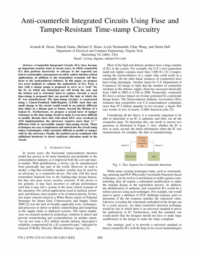
At low cost, seals provide a simple way to distinguish usedICs from new ones. Analogous to the seals used in medicinebottles to determine if the bottle has been opened and used,we propose an inexpensive technique to implement a sealvia a standard fuse and a charge pump. Although fuses havebeen used for various applications on ICs, to the best of ourknowledge, no work has been proposed in the context of anti-counterfeiting.
Fig. 2: Use of fuse
A fuse is a standard component provided by the foundry.The voltage that is required to blow the fuse can be easilyproduced using a simple charge pump circuitry. Figure 2shows a fuse-based design with a basic charge pump. Althoughbridging a fuse might be possible with techniques like sputter-ing deposition using focused ion beams, the associated costsoutweigh the benefits the counterfeiter gets from fake ICs.
When an IC is equipped with a fuse and a charge pump,the process of evaluating if an IC is used or new can beincorporated into the DFT mechanism of the chip or it candirectly be accomplished through the pins of an IC. The basicactions that are essential are: (1) check the status of the fuseand to (2) blow the fuse.
Check Fuse This command is used to check if the fuseis intact or blown. Check fuse is as simple as performing acontinuity check across fuse terminals. This is analogous tochecking if the seal of the medicine bottle is intact.
Blow Fuse Once an IC equipped with a fuse becomes afunctional part of a board, the fuse is automatically blown onits first use. A charge pump is used to blow the fuse. A varietyof charge pumps are presented in the literature and Figure 2shows a one stage charge pump circuit. The operation of the
481
charge pumps is presented in [22], and [23] shows a low costimplementation of a charge pump in a CMOS process.
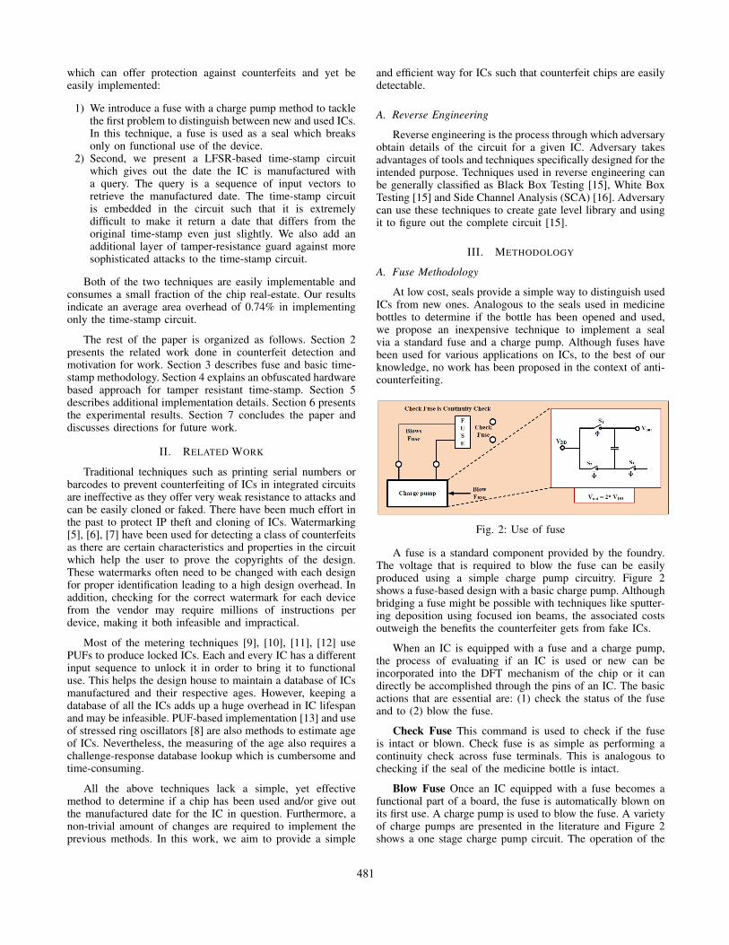
One problem with ”blow fuse” is that the fuse has tostay intact during the post manufacturing test of the IC andit should only be blown after it becomes part of a workingboard. To accomplish this, a circuit such as the pseudo-nmoscircuit shown in Figure 3 can be leveraged. During the testingof the IC by the manufacturer and by the original equipmentmanufacturer (OEM), the blow fuse signal remains low asPMT (Post Manufacturing Test signal) is an active high signaland as PMT dominates the weak pull down resistor R1. Whenthe IC becomes part of a board, PMT is a high impedancesignal and R1 keeps the transistor N1 OFF. As a result, blowfuse is set high as CL charges to V DD. The charge pumpoutput voltage can be transferred to the fuse terminal throughN2 pass gate as shown in Figure 3.
To ensure that fuse blows, PMT should not be accessible orcontrolled by the user/board that the IC becomes part of. So,instead of making PMT as an input pin, it can be set throughthe DFT elements of the IC which the user never can get accessto. The control sequence to assert PMT is only provided to therelated testing parties.
PMT
Blow Fuse
VDD
CLR1
P1 – weak pmos, always ON
R1 – weak pull down resistor
PMT – active high signal
N2 – pass transistorP1
N2
Charge Pump
output Fuse terminal
N1
Fig. 3: Circuit enabling blow fuse
A blown fuse indicates that the device has been used,thus it is not fresh out of fab. The cost for an adversaryto repair/replace the fuse should be much higher than thebenefits they would get in return for selling counterfeits. Inthe proposed fuse, it is exactly that. The cost of repairing ablown fuse would outweigh the benefits of selling a counterfeitdevice.
In addition to the fuse, we would also like to know ifthe device was in fact manufactured in the latest batch andnot from a pool of devices manufactured a number of yearsago. In both fresh chip pools, the fuses would remain intactsince neither has been used. To determine if a chip is newlymanufactured or not, a time-stamp is proposed, which isdiscussed next.
B. Time-Stamp Circuit
In this section, we address the counterfeit problem with anovel time-stamp methodology as a hybrid anti-tamper andcounterfeit detection. The time-stamp by itself can offer themanufacturing date, and the surrounding anti-tamper circuitrymakes it difficult even for more sophisticated attacks to modifythe time-stamp. Our proposed method involves the use of an
entry mode path traversals as in Anti-Tamper methods [14],[17], [18], [19] and a low area-overhead Linear FeedbackShift Register (LFSR) circuit with a custom tap configurationthat will generate the manufactured date. A specific path inthe entry mode is traversed so that the circuit gives out theembedded manufacturing date. In addition to the date, the time-stamp can also include information such as version, fab, etc.
A LFSR is a register whose next state is a linear functionof its previous state. The commonly used linear function forbuilding LFSR is the XOR function. The initial value ofthe LFSR is called a “seed.” The next state of the LFSR iscompletely determined by its present state. A LFSR has afinite number of states, hence it eventually enters in a cycle ofrepeating states. However, the length of the cycle is generallyvery long. For example, an n-bit LFSR with a properly chosenconfiguration can loop through a cycle of up to 2n − 1 states.They have been useful for Logic Built In Self Test (LBIST)[20], [21] and random number generation. LFSR structure iseasy to design but it is extremely difficult to reverse engineerbecause a large combination of seeds and tap configuration canlead to a certain state.
Our time-stamp uses a LFSR in a non-conventional mannerwhere the configuration does not allow for the maximumnumber of possible states (2n − 1). The tap configuration ofthe LFSR is designed such that the possible number of statesof the LFSR is limited. The key feature of this configurationis that the values that can be produced in the LFSR at the endof ‘m’ transitions is a finite set of values, {v1, v2, ..., vk}.Let these values denote the year for simplicity of discussion.Then, one of the values vi is 2013. And all other values in theset has a distance from vi of at least d. That is, the nearestyear that can be represented from this set is either 2013+d or2013−d.
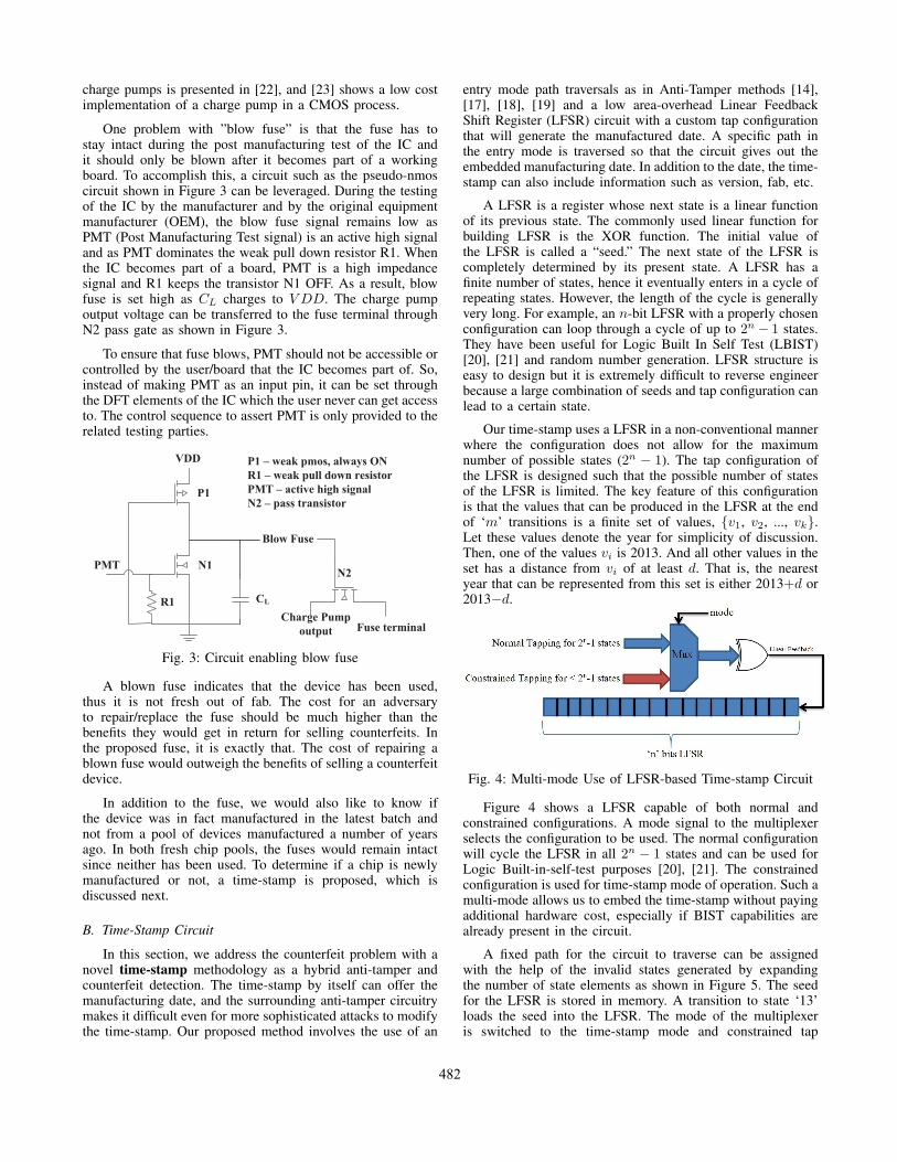
Fig. 4: Multi-mode Use of LFSR-based Time-stamp Circuit
Figure 4 shows a LFSR capable of both normal andconstrained configurations. A mode signal to the multiplexerselects the configuration to be used. The normal configurationwill cycle the LFSR in all 2n − 1 states and can be used forLogic Built-in-self-test purposes [20], [21]. The constrainedconfiguration is used for time-stamp mode of operation. Such amulti-mode allows us to embed the time-stamp without payingadditional hardware cost, especially if BIST capabilities arealready present in the circuit.
A fixed path for the circuit to traverse can be assignedwith the help of the invalid states generated by expandingthe number of state elements as shown in Figure 5. The seedfor the LFSR is stored in memory. A transition to state ‘13’loads the seed into the LFSR. The mode of the multiplexeris switched to the time-stamp mode and constrained tap
482
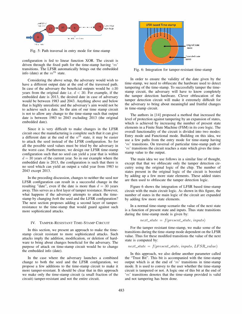
Fig. 5: Path traversal in entry mode for time-stamp
configuration is fed to linear function XOR. The circuit isdriven through the fixed path for the time-stamp having ‘m’transitions. The LFSR automatically brings out the embeddedinfo (date) at the mth state.
Considering the above setup, the adversary would wish tohave a different output date at the end of the traversed path.In case of the adversary the beneficial outputs would be ±30years from the original date i.e. d < 30. For example, if theembedded date is 2013, the desired date in case of adversarywould be between 1983 and 2043. Anything above and belowthat is highly unrealistic and the adversary’s aim would not beto achieve such a date. So the aim of our time stamp circuitis not to allow any change to the time-stamp such that outputdate is between 1983 to 2043 excluding 2013 (the originalembedded date).
Since it is very difficult to make changes in the LFSRcircuit once the manufacturing is complete such that it can givea different date at the end of the nth state, it may be easierto attack the seed instead of the LFSR configuration. So forall the possible seed values must be tried by the adversary inthe worst case. Furthermore, we design our LFSR time-stampconfiguration such that no seed can yield a year that is withind = 30 years of the current year. So in our example where theembedded date is 2013, the configuration is such that there isno seed which can yield an output a valid year from 1983 to2043 except 2013.
In the preceding discussion, changes to neither the seed norLFSR configuration can result in a successful change in theresulting ”date”, even if the date is more than d = 30 yearsaway. This serves as a first layer of tamper resistance. However,what happens if the adversary attempts to attack the time-stamp by changing both the seed and the LFSR configuration?The next section proposes adding a second layer of tamper-resistance to the time-stamp that would guard against suchmore sophisticated attacks.
IV. TAMPER-RESISTANT TIME-STAMP CIRCUIT
In this section, we present an approach to make the time-stamp circuit resistant to more sophisticated attacks. Suchattacks imply the addition, modification, or deletion of hard-ware to bring about changes beneficial for the adversary. Thepurpose of attack on time-stamp circuit would be to changethe embedded info (date).
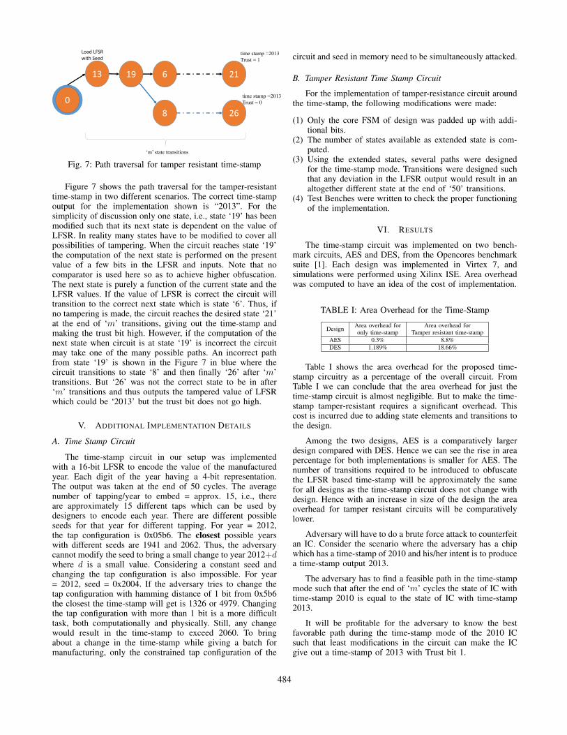
In the case where the adversary launches a combinedchange to both the seed and the LFSR configuration, wepropose a few additions to the time-stamp circuit to make itmore tamper-resistant. It should be clear that in this approachwe make only the time-stamp circuit (a small fraction of thecircuit) tamper-resistant and not the entire circuit.
Fig. 6: Integration for tamper-resistant time-stamp
In order to ensure the validity of the date given by thetime-stamp, we need to obfuscate the hardware used to detecttampering of the time-stamp. To successfully tamper the time-stamp circuit, the adversary will have to know completelythe tamper detection hardware. Clever obfuscation of thetamper detection circuit will make it extremely difficult forthe adversary to bring about meaningful and fruitful changesin time-stamp circuit.
The authors in [14] proposed a method that increased thelevel of protection against tampering by an expansion of states,which is achieved by increasing the number of present stateelements in a Finite State Machine (FSM) in its core logic. Theoverall functionality of the circuit is divided into two modes:Entry mode and Functional mode. Building on this idea, weuse a few paths from the entry mode for time-stamp having‘m’ transitions. On traversal of particular time-stamp path of‘m’ transitions the circuit reaches a state which gives the time-stamp value to the output.
The main idea we use follows in a similar line of thought,except that that we obfuscate only the tamper detection cir-cuitry using the original logic of the chip. The number ofstates present in the original logic of the circuit is boostedby adding up a few more state elements. These added statesare then used to obfuscate the tamper detection logic.
Figure 6 shows the integration of LFSR based time-stampcircuit with the main circuit logic. As shown in this figure, thenumber of states in the main logic of the circuit are expandedby adding few more state elements.
In a normal time-stamp scenario the value of the next stateis a function of present state and inputs. Thus state transitionsduring the time-stamp mode is given by:
next state = f(present state, inputs)
For the tamper resistant time-stamp, we make some of thetransitions during the time-stamp mode dependent on the LFSRvalue. Thus for these modified transitions the value of the nextstate is computed by:
next state = f(present state, inputs, LFSR value)
In this approach, we also define another parameter calledthe “Trust Bit”. This bit is accompanied with the time-stampoutput which is at the end of ‘m’ transitions in time-stampmode. It is used to convey to the user whether the time-stampcircuit is tampered or not. A logic one of this bit at the end of‘m’ transitions denotes that the time-stamp provided is validand not tampering has been done.
483
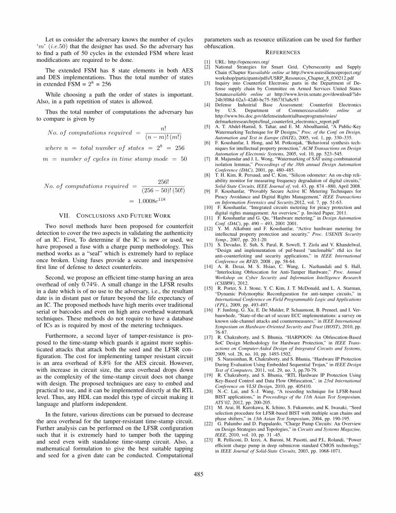
0
13 19 6
8
21
26
Load LFSR
with Seed
‘m’ state transitions
time stamp =2013
Trust = 1
time stamp =2013
Trust = 0
Fig. 7: Path traversal for tamper resistant time-stamp
Figure 7 shows the path traversal for the tamper-resistanttime-stamp in two different scenarios. The correct time-stampoutput for the implementation shown is “2013”. For thesimplicity of discussion only one state, i.e., state ‘19’ has beenmodified such that its next state is dependent on the value ofLFSR. In reality many states have to be modified to cover allpossibilities of tampering. When the circuit reaches state ‘19’the computation of the next state is performed on the presentvalue of a few bits in the LFSR and inputs. Note that nocomparator is used here so as to achieve higher obfuscation.The next state is purely a function of the current state and theLFSR values. If the value of LFSR is correct the circuit willtransition to the correct next state which is state ‘6’. Thus, ifno tampering is made, the circuit reaches the desired state ‘21’at the end of ‘m’ transitions, giving out the time-stamp andmaking the trust bit high. However, if the computation of thenext state when circuit is at state ‘19’ is incorrect the circuitmay take one of the many possible paths. An incorrect pathfrom state ‘19’ is shown in the Figure 7 in blue where thecircuit transitions to state ‘8’ and then finally ‘26’ after ‘m’transitions. But ‘26’ was not the correct state to be in after‘m’ transitions and thus outputs the tampered value of LFSRwhich could be ‘2013’ but the trust bit does not go high.
V. ADDITIONAL IMPLEMENTATION DETAILS
A. Time Stamp Circuit
The time-stamp circuit in our setup was implementedwith a 16-bit LFSR to encode the value of the manufacturedyear. Each digit of the year having a 4-bit representation.The output was taken at the end of 50 cycles. The averagenumber of tapping/year to embed = approx. 15, i.e., thereare approximately 15 different taps which can be used bydesigners to encode each year. There are different possibleseeds for that year for different tapping. For year = 2012,the tap configuration is 0x05b6. The closest possible yearswith different seeds are 1941 and 2062. Thus, the adversarycannot modify the seed to bring a small change to year 2012+dwhere d is a small value. Considering a constant seed andchanging the tap configuration is also impossible. For year= 2012, seed = 0x2004. If the adversary tries to change thetap configuration with hamming distance of 1 bit from 0x5b6the closest the time-stamp will get is 1326 or 4979. Changingthe tap configuration with more than 1 bit is a more difficulttask, both computationally and physically. Still, any changewould result in the time-stamp to exceed 2060. To bringabout a change in the time-stamp while giving a batch formanufacturing, only the constrained tap configuration of the
circuit and seed in memory need to be simultaneously attacked.
B. Tamper Resistant Time Stamp Circuit
For the implementation of tamper-resistance circuit aroundthe time-stamp, the following modifications were made:
(1) Only the core FSM of design was padded up with addi-tional bits.
(2) The number of states available as extended state is com-puted.
(3) Using the extended states, several paths were designedfor the time-stamp mode. Transitions were designed suchthat any deviation in the LFSR output would result in analtogether different state at the end of ‘50’ transitions.
(4) Test Benches were written to check the proper functioningof the implementation.
VI. RESULTS
The time-stamp circuit was implemented on two bench-mark circuits, AES and DES, from the Opencores benchmarksuite [1]. Each design was implemented in Virtex 7, andsimulations were performed using Xilinx ISE. Area overheadwas computed to have an idea of the cost of implementation.
TABLE I: Area Overhead for the Time-Stamp
Design Area overhead for Area overhead foronly time-stamp Tamper resistant time-stamp
AES 0.3% 8.8%DES 1.189% 18.66%
Table I shows the area overhead for the proposed time-stamp circuitry as a percentage of the overall circuit. FromTable I we can conclude that the area overhead for just thetime-stamp circuit is almost negligible. But to make the time-stamp tamper-resistant requires a significant overhead. Thiscost is incurred due to adding state elements and transitions tothe design.
Among the two designs, AES is a comparatively largerdesign compared with DES. Hence we can see the rise in areapercentage for both implementations is smaller for AES. Thenumber of transitions required to be introduced to obfuscatethe LFSR based time-stamp will be approximately the samefor all designs as the time-stamp circuit does not change withdesign. Hence with an increase in size of the design the areaoverhead for tamper resistant circuits will be comparativelylower.
Adversary will have to do a brute force attack to counterfeitan IC. Consider the scenario where the adversary has a chipwhich has a time-stamp of 2010 and his/her intent is to producea time-stamp output 2013.
The adversary has to find a feasible path in the time-stampmode such that after the end of ‘m’ cycles the state of IC withtime-stamp 2010 is equal to the state of IC with time-stamp2013.
It will be profitable for the adversary to know the bestfavorable path during the time-stamp mode of the 2010 ICsuch that least modifications in the circuit can make the ICgive out a time-stamp of 2013 with Trust bit 1.
484
Let us consider the adversary knows the number of cycles‘m’ (i.e.50) that the designer has used. So the adversary hasto find a path of 50 cycles in the extended FSM where leastmodifications are required to be done.
The extended FSM has 8 state elements in both AESand DES implementations. Thus the total number of statesin extended FSM = 28 = 256
While choosing a path the order of states is important.Also, in a path repetition of states is allowed.
Thus the total number of computations the adversary hasto compare is given by
No. of computations required =n!
(n−m)! (m!)
where n = total number of states = 28 = 256
m = number of cycles in time stamp mode = 50
No. of computations required =256!
(256− 50)! (50!)
= 1.0008e118
VII. CONCLUSIONS AND FUTURE WORK
Two novel methods have been proposed for counterfeitdetection to cover the two aspects in validating the authenticityof an IC. First, To determine if the IC is new or used, wehave proposed a fuse with a charge pump methodology. Thismethod works as a “seal” which is extremely hard to replaceonce broken. Using fuses provide a secure and inexpensivefirst line of defense to detect counterfeits.
Second, we propose an efficient time-stamp having an areaoverhead of only 0.74%. A small change in the LFSR resultsin a date which is of no use to the adversary, i.e., the resultantdate is in distant past or future beyond the life expectancy ofan IC. The proposed methods have high merits over traditionalserial or barcodes and even on high area overhead watermarktechniques. These methods do not require to have a databaseof ICs as is required by most of the metering techniques.
Furthermore, a second layer of tamper-resistance is pro-posed to the time-stamp which guards it against more sophis-ticated attacks that attack both the seed and the LFSR con-figuration. The cost for implementing tamper resistant circuitis an area overhead of 8.8% for the AES circuit. However,with increase in circuit size, the area overhead drops downas the complexity of the time-stamp circuit does not changewith design. The proposed techniques are easy to embed andpractical to use, and it can be implemented directly at the RTLlevel. Thus, any HDL can model this type of circuit making itlanguage and platform independent.
In the future, various directions can be pursued to decreasethe area overhead for the tamper-resistant time-stamp circuit.Further analysis can be performed on the LFSR configurationsuch that it is extremely hard to tamper both the tappingand seed even with standalone time-stamp circuit. Also, amathematical formulation to give the best suitable tappingand seed for a given date can be conducted. Computational
parameters such as resource utilization can be used for furtherobfuscation.
REFERENCES
[1] URL: http://opencores.org/[2] National Strategies for Smart Grid, Cybersecurity and Supply
Chain (Chapter 8)available online at http://www.usresilienceproject.org/workshop/participants/pdfs/USRP Resources Chapter 8 030212.pdf
[3] Inquiry into Counterfeit Electronic parts in the Department of De-fense supply chain by Committee on Armed Services United StatesSenateavailable online at http://www.levin.senate.gov/download/?id=24b3f08d-02a3-42d0-bc75-5f673f3a8c93
[4] Defense Industrial Base Assessment: Counterfeit Electronicsby U.S. Department of Commerceavailable online athttp://www.bis.doc.gov/defenseindustrialbaseprograms/osies/defmarketresearchrpts/final counterfeit electronics report.pdf
[5] A. T. Abdel-Hamid, S. Tahar, and E. M. Aboulhamid, “A Public-KeyWatermarking Technique for IP Designs,” Proc. of the Conf. on Design,Automation and Test in Europe (DATE), 2005, vol. 1, pp. 330–335.
[6] F. Koushanfar, I. Hong, and M. Potkonjak, “Behavioral synthesis tech-niques for intellectual property protection,” ACM Transactions on DesignAutomation of Electronic Systems, 2005, vol. 10, pp. 523–545.
[7] R. Majumdar and J. L. Wong, “Watermarking of SAT using combinatorialisolation lemmas,” Proceedings of the 38th annual Design AutomationConference (DAC), 2001, pp. 480–485.
[8] T. H. Kim, R. Persaud, and C. Kim, “Silicon odometer: An on-chip reli-ability monitor for measuring frequency degradation of digital circuits,”Solid-State Circuits, IEEE Journal of, vol. 43, pp. 874 –880, April 2008.
[9] F. Koushanfar, “Provably Secure Active IC Metering Techniques forPiracy Avoidance and Digital Rights Management,” IEEE Transactionson Information Forensics and Security,2012, vol. 7, pp. 51-63.
[10] F. Koushanfar, “Integrated circuits metering for piracy protection anddigital rights management: An overview,” p. Invited Paper, 2011.
[11] F. Koushanfar and G. Qu, “Hardware metering,” in Design AutomationConf. (DAC), pp. 490 – 493, 2001 2001.
[12] Y. M. Alkabani and F. Koushanfar, “Active hardware metering forintellectual property protection and security,” Proc. USENIX SecuritySymp., 2007, pp. 20:1-20.
[13] S. Devadas, E. Suh, S. Paral, R. Sowell, T. Ziola and V. Khandelwal,“Design and implementation of puf-based “unclonable” rfid ics foranti-counterfeiting and security applications,” in IEEE InternationalConference on RFID, 2008 , pp. 58-64.
[14] A. R. Desai, M. S. Hsiao, C. Wang, L. Nazhandali and S. Hall,“Interlocking Obfuscation for Anti-Tamper Hardware,” Proc. AnnualWorkshop on Cyber Security and Information Intelligence Research(CSIIRW), 2012.
[15] R. Porter, S. J. Stone, Y. C. Kim, J. T. McDonald, and L. A. Starman,“Dynamic Polymorphic Reconfiguration for anti-tamper circuits,” inInternational Conference on Field Programmable Logic and Applications(FPL), 2009, pp. 493-497.
[16] F. Junfeng, G. Xu, E. De Mulder, P. Schaumont, B. Preneel, and I. Ver-bauwhede, “State-of-the-art of secure ECC implementations: a survey onknown side-channel attacks and countermeasures,” in IEEE InternationalSymposium on Hardware-Oriented Security and Trust (HOST), 2010, pp.76-87.
[17] R. Chakraborty, and S. Bhunia, “HARPOON: An Obfuscation-BasedSoC Design Methodology for Hardware Protection,” in IEEE Trans-actions on Computer-Aided Design of Integrated Circuits and Systems,2009, vol. 28, no. 10, pp. 1493-1502.
[18] S. Narasimhan, R. Chakraborty, and S. Bhunia, “Hardware IP ProtectionDuring Evaluation Using Embedded Sequential Trojan,” in IEEE DesignTest of Computers, 2011, vol. 29, no. 3, pp.70-79.
[19] R. Chakraborty, and S. Bhunia, “RTL Hardware IP Protection UsingKey-Based Control and Data Flow Obfuscation,”. in 23rd InternationalConference on VLSI Design, 2010, pp. 405410.
[20] N.-C. Lai, and S.-J. Wang, “A reseeding technique for LFSR-basedBIST applications,” in Proceedings of the 11th Asian Test Symposium,ATS’02, 2012, pp. 200-205.
[21] M. Arai, H. Kurokawa, K. Ichino, S. Fukumoto, and K. Iwasaki, “Seedselection procedure for LFSR-based BIST with multiple scan chains andphase shifters,” in 13th Asian Test Symposium, 2004, pp. 190-195.
[22] G. Palumbo and D. Pappalardo, “Charge Pump Circuits: An Overviewon Design Strategies and Topologies,” in Circuits and Systems Magazine,IEEE, 2010, vol. 10, pp. 31 -45.
[23] R. Pelliconi, D. Iezzi, A. Baroni, M. Pasotti, and P.L. Rolandi, “Powerefficient charge pump in deep submicron standard CMOS technology,”in IEEE Journal of Solid-State Circuits, 2003, pp. 1068-1071.
485