Embed Size (px)
Citation preview

1. (b)
2. (c)
3. (d)
4. (c)
5. (c)
6. (b)
7. (c)
8. (b)
9. (b)
10. (b)
11. (d)
12. (a)
13. (a)
14. (c)
15. (c)
16. (d)
17. (b)
18. (c)
19. (a)
20. (a)
21. (d)
22. (a)
ESE-2019 PRELIMS TEST SERIESDate: 18th November, 2018
23. (a)
24. (a)
25. (a)
26. (d)
27. (b)
28. (c)
29. (b)
30. (c)
31. (c)
32. (a)
33. (b)
34. (c)
35. (c)
36. (b)
37. (d)
38. (c)
39. (a)
40. (a)
41. (c)
42. (c)
43. (a)
44. (b)
45. (b)
46. (a)
47. (b)
48. (b)
49. (a)
50. (d)
51. (c)
52. (b)
53. (b)
54. (a)
55. (b)
56. (d)
57. (d)
58. (b)
59. (b)
60. (d)
61. (c)
62. (b)
63. (d)
64. (b)
65. (c)
66. (a)
ANSWERS
67. (b)
68. (a)
69. (c)
70. (a)
71. (b)
72. (d)
73. (b)
74. (c)
75. (b)
76. (c)
77. (d)
78. (c)
79. (b)
80. (c)
81. (b)
82. (b)
83. (d)
84. (d)
85. (c)
86. (b)
87. (c)
88. (a)
89. (b)
90. (c)
91. (b)
92. (a)
93. (d)
94. (c)
95. (a)
96. (d)
97. (c)
98. (b)
99. (a)
100. (d)
101. (c)
102. (d)
103. (b)
104. (b)
105. (a)
106. (a)
107. (c)
108. (a)
109. (c)
110. (b)
111. (a)
112. (c)
113. (a)
114. (c)
115. (c)
116. (d)
117. (c)
118. (a)
119. (b)
120. (d)
121. (b)
122. (c)
123. (c)
124. (b)
125. (c)
126. (d)
127. (d)
128. (b)
129. (b)
130. (a)
131. (b)
132. (b)
133. (a)
134. (c)
135. (d)
136. (b)
137. (d)
138. (d)
139. (c)
140. (d)
141. (a)
142. (a)
143. (c)
144. (c)
145. (a)
146. (a)
147. (c)
148. (c)
149. (c)
150. (a)

IES M
ASTER
(2)
1. (b)
2. (c)3. (d) It causes broadning of ion beam
4. (c)
5. (c)
6. (b)
7. (c)
8. (b)
9. (b)10. (b)
11. (d)
12. (a)
13. (a)14. (c)
Optical lithography has high throughput goodresolution low cost and ease in operation . Itprovides good resolution but highest resolutionis provided by lon beam lithography limitationis complexity of mask production.
15. (c)For example N bit counter
16. (d)17. (b)
×
×
LDo
LDo
LDo
A
B
C
×
×
×
×
×
×
×
×
×
×
×
× ×
××
18. (c)
19. (a)
1 K = 210 and 16 = 2 bytes, 2 k bytes = 2048
20. (a)
21. (d)
22. (a)
23. (a)24. (a)
T1
T2
T4
T4T3
T2
T11/0
1
1/0
1
1/0
0
1/0
0
1/0
1
a
a/0
b
b/0
Rules to convert Mealy to Moore Model1. If all the transitions in a Mealy model to a
particular state are associated with only onetype of output (0 or 1) then in correspondingmoore model that output becomes stak output.
2. If the outputs of all tansitions in a mealy modelto a particular state are not same we need toinsert intermediate state variables.T1
T1
T2
T3
T4
T4
1/0
1
1/0
0
0/1
1
1
0/0
1
1/1
0
0
a
a/0
a /12
b/0
bT2
T3

IES M
ASTER
[EC], ESE-2019 PRELIMS TEST SERIES PAPER-II (TEST-09) (3)
25. (a)
26. (d)
8254 programmable interval timer/counteris functionally similar to the softwaredesigned counters and timers.
it generates accurate time delay and it canbe used for applications such
(1) real-time clock
(2) event counter
(3) digital one shot
(4) square wave generator
(5) complex waveform generator
27. (b)
It is short abbreviation for the operation to beperformed.
28. (c)
We know that
Address bus : It is a uni-directional bus
Data bus : Bi-directional Bus
Control Bus : Bi-directional bus.
29. (b)
MVI, 80 H
A80 H
A1000 0000
RAR (Rotate accumulator right with carry)
0 1 0 0 0 0 0 0cy0
A 40 HSIM (Set interrupt mask)
SOD
0 1 0 0 0 0 0 0
SDE R7.5
M7.5
M6.5
M5.5MSE
Serialoutput bitSerial data enable=1
Reset MSE = 0 (Mask set disabled)
30. (c) MVI A, 18 H
A 18 H A = 1×16+8 = (24)10
A 0001 1000
RLC (Rotate left without carry)
0 0 1 1 0 0 0 0cy0
A 30 H
A = 3×16’+0×16°
A = (48)10
31. (c)
(1) MVI A, C5H
A C5H
(2) ORA A
A 1100 0101
1100 0101
A 1100 0101
A C5H
(3) RAL (Rotate accumulator Left with carry)cy1
1 0 0 0 1 0 1 0
AA (8A)H
8
(4) RRC (Rotate right with out carry)cy0
0 1 0 0 0 1 0 1
5A (45)H
4
32. (a)
TRAP :
(i) highest priority
(ii) only non-maskable interrupt
(iii) vectored interrupt
(iv) both positive edge an level triggered
(v) a hardware interrupt
33. (b)
Instruction register holds opcode of presentinstruction being executed. It is a 8-bit, user notaccessible register.
34. (c)

IES M
ASTER
(4)
8-bit resgisters :
• Accumulator
• Status/Flag register
• Temporary registers
• B, C, D, E, H & L
• Instruction register
16-bit registers :
• Program counter
• Stack pointer
• Increment/Decrement Address register.
35. (c)
In 8085 P , number of output pins = 27
and, number of input pins = 21
48
Note : AD0 - AD7 are taken as both input andoutput pins.
36. (b)
Soft interrupts : RST n
where n = 0 to 7
37. (d)
The programmable interrupt controller 8259 isused when several I/O devices transfer datausing interrupt.
38. (c)
For 8K × 8 memory, the address lines
= 3 102 2
= 132
i.e. 13 address lines are required.
39. (a)
Machine cycles for CALL instruction
= One opcode fetch + 2 memory read
+ 2 memory write
40. (a)
41. (c)For notch filter, we have to compress mag-
nitude spectrum of jH e such that 2 is
shifted to 4
A(z) = H(zn)
2n
= 4
n = 8
42. (c)Window effectively truncates the ideal im-pulse response. Hence peaks are observedat transition frequency.
43. (a)Hamming window leads to minimum peakside lobe.
44. (b)
Since all poles are at z , system is FIR
It may not be linear phase but it can bemade linear phase.
45. (b)
x3(k) = x1[n]x2[n]
= 60 0 4 0
x3[n] = 3
j2 nk 43k 0
x ek
= j n160 4e4
x3[0] = 4, x3[1] = 16, x3[2] = 14, x3[3] = 16
46. (a)Both algorithms give same result and arebased on divide and conquer approach.
47. (b)Single chip has 8 inputs
for 24 inputs, 3 chips are required.
48. (b)4 in first stage, 4 in second stage and 4 inthird stage.
49. (a)Both statements are correct.
50. (d)
Multiplications - 2N log N2

IES M
ASTER
[EC], ESE-2019 PRELIMS TEST SERIES PAPER-II (TEST-09) (5)
additions - Nlog2N
51. (c)
From properties of cumulative distributionfunction, we have
0 F (x) 1
xF ( ) 0
xF ( ) 1
52. (b)
Mean of random variable X is given as
=
x
–
xf (x)dx
Since X is uniformly distributed between p andq
fx(x) = 1 ,p x q
q p
= q
p
1x. dxq p
=
q2
p
x 1.2 q p
=
2 2q p 1 p q.2 q p 2
53. (b)
We have Per =
inc
V1 erf2 2 2
= c c
1 6 1 3erf erf2 2 22 2 2
54. (a)
If two jointly Guassian processes areuncorrelated then they are statistical lyindependent.
55. (b)
The Power Spectral Density (PSD) of white noisehas constant value No/2 for all frequencies.Since, the area under PSD curve is equal tototal average power, hence average power ofwhite noise process is infinite.
56. (d)
From the definition, two process are jointlystationary if they are individually stationary andif their cross-correlation is function of (t1–t2) only.
57. (d)
Variance of random variable Y with mean y is
2Var Y = 2
yE Y
= 2 2y yE Y 2E Y
= 22E Y E Y
58. (b)
Poisson distribution is given as
Px(K) =k
e ,where TK!
Which is probability of K occurance in time T.
Mean and variance of poisson distribution
= 2
Here, given 27 7
59. (b)
Available noise power Pa = KTB watts, which isindependent of R.
60. (d)
As flicker noise 1f
, hence effective at low
frequencies Transit-time noise is important athigh frequency. Noise generated in resistor iscalled thermal noise. White noise is independentof frequency
61. (c)
Noise temperature Tn= T (F–1)
= 300 × (1.75–1)
= 300 × 0.75
= 225K
62. (b)
Given channel loss = 10dB

IES M
ASTER
(6)
dB
Received powerTransmitted power
= –10
r10
t
P10log
P = –10
r
t
PP = 10–1
Pr = Pt × 10–1 = 5 × 0.1 = 0.5 W
63. (d)
For a PCM system, signal to quantization noiseratio
q dB
SN
= 6n + 1.8
For 8 bit PCM q dB
SN
= 6×8+1.8=49.8 dB
For 10 bit PCM q dB
SN
=6×10 1.8=61.8 dB
improvement in q dB
SN
=61.8–49.8=12 dB
64. (b)
Since each signal is band limited to fm, we haveto take 2fm samples per second. For n signals,2nfm samples per second are required to betransmitted, hence as per sampling theorem,bandwidth of PAM system will be 2nfm Hz.
65. (c)
The spectrum of x(2t) streches to 10kHz. Hence,the Nyquist rate = 10 × 2 = 20KHz
66. (a)
Sampling frequency fs 2fm
fs 2 × 1.6 KHz
s bnf R = 18000
b
s
Rn
f =
18000 5.63200
n = 5
fs= bR 18000 3.6KHzn 5
67. (b)
For a raised-cosine pulse, data rate is
Rb =1 2BT 1
[B = Band width = 35KHz]
=2 35 1000 56kbps
1 0.25
68. (a)
For a raised cosine pulses
B = zb
1 H2T
Here we have B = 100 KHz
Rb =b
10.2MbpsT
Tb =6
61 5 10 second
0.2 10
B =b
12T
1 = 2B Tb
1 = 2×100×103 ×5×10–6
1 = 1
= 0
(Ideal low pass filter)
69. (c)
For a PCM system given q dB,min
SN
= 40dB
q
SN = 10000
or 23 LL = 10000

IES M
ASTER
[EC], ESE-2019 PRELIMS TEST SERIES PAPER-II (TEST-09) (7)
or L = 2 100003 or
L = 81.6 = 2n
n = 7
70. (a)
DM transmitter and receiver require very simpleand inexpensive hardware.
71. (b)
In Mid-tread type quantizer
any input value between
0.5 to 0.5 mapped to 0
any input value bwtween
mappedto0.5 to 1.5 1
72. (d)
Half slot-width duration positive and negativepulses are used for representing alternate binaryand no pulse is used for representing the binary0 in Bipolar return to zero, also known as AMIcode
73. (b)
Unipolar non return to zero large dccomponent
Unipolar return to zero Bit timing recoveryat receiver
Bipolar return to zero in built error detectingcapability against sign inversion
Split phase – No dc component
74. (c)
PSK requires coherent detection
75. (b)For a given bit energy, non coherent ASK givesmaximum probability of error
76. (c)For BPSK system, probability of error is givenas
Pe = bE1 erfc
2
77. (d)
For M-ary system log2 M = b
T
R 60 4B 15
log2 M = 4
M = 24 = 16
78. (c)
MSK is a type of continuous-phase FSK thatproduces orthogonal signalling.
79. (b)
To achieve a specified probability of error, ASKrequires twice the pulse energy as compared toPSK i.e. 3 dB more power than PSK.
80. (c)
BFSK QPSKBW 4 BW
81. (b)
Here, B = 2 × 10⁶ Hz
SNR = 31
Channel capacity
C = B log2(1 + SNR)bits/sec
C = 2 × 10⁶ log2(1 + 31)bits/sec
= 2 × 10⁶ log232 bits/sec
= 10 × 106 bits/sec
Data rate (20 × 106 bits/sec) > channelcapacity
Data transmitted will have errors.
82. (b)Here, channel capacity C = 256 × 103 bits/sec
Now, C = B log2(1 + SNR) bits/sec
(SNR)dB = 20dB
10log10SNR = 20
SNR = 100
B = 2
Clog (1 SNR)
= 3
2
256 10log 101
= 38.45 kHz
83. (d)
All the three statements are correct.
IES M
ASTER
(8)
Modulation is used for frequency translation,Multiplexing reducing antenna height andconverts wide-band signal to narrow bandsignal.
84. (d)When modulation index in AM is greater than1, the envelope is distorted and does notcontain actual message.
For a SSB-SC, the bandwidth of modulatedsignal is equal to B.W. of message signal
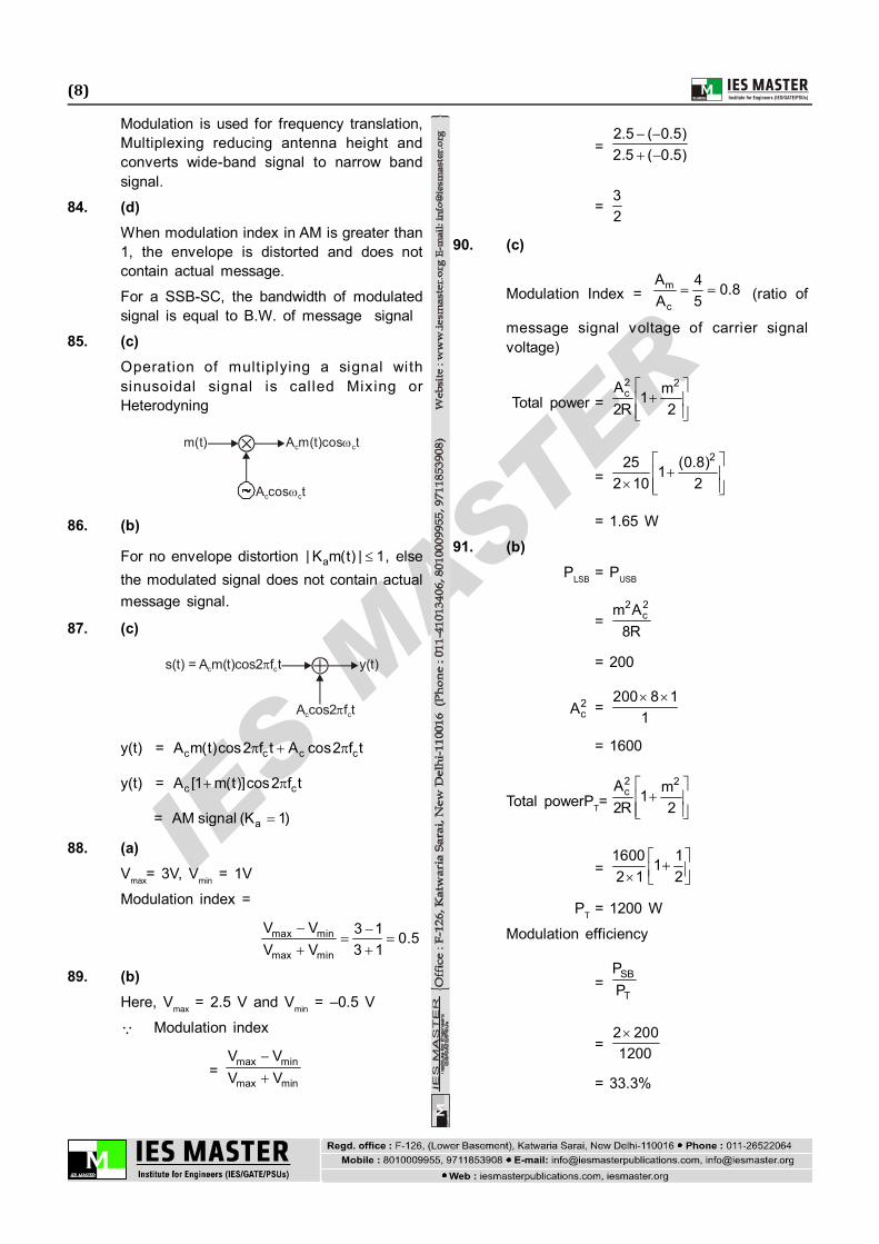
85. (c)Operation of multiplying a signal withsinusoidal signal is cal led Mixing orHeterodyning
m(t)
A cos tc c
A m(t)cos tc c
86. (b)
For no envelope distortion a| K m(t) | 1, elsethe modulated signal does not contain actualmessage signal.
87. (c)
y(t)
A cos2 tc cf
s(t) = A m(t)cos2 tc cf
y(t) = c c c cA m(t)cos2 f t A cos2 f t
y(t) = c cA [1 m(t)]cos2 f t
= aAM signal (K 1)
88. (a)Vmax= 3V, Vmin = 1V
Modulation index =
max min
max min
V V 3 1 0.5V V 3 1
89. (b)Here, Vmax = 2.5 V and Vmin = –0.5 V
Modulation index
=
max min
max min
V VV V
=
2.5 ( 0.5)2.5 ( 0.5)
=32
90. (c)
Modulation Index = m
c
A 4 0.8A 5 (ratio of
message signal voltage of carrier signalvoltage)
Total power =
2 2cA m1
2R 2
=
225 (0.8)12 10 2
= 1.65 W
91. (b)PLSB = PUSB
=2 2
cm A8R
= 200
2cA =
200 8 11
= 1600
Total powerPT=
2 2cA m1
2R 2
=
1600 112 1 2
PT = 1200 W
Modulation efficiency
=SB
T
PP
=2 200
1200
= 33.3%

IES M
ASTER
[EC], ESE-2019 PRELIMS TEST SERIES PAPER-II (TEST-09) (9)
92. (a)
PT =
2
CmP 12
PT =
2
C(0.5)P 1
2
PC = 0.89PT
89% is carrier power and hence 11% issideband power.
93. (d)
Total power in AM = PT =
2
CmP 12
As m increases PT increases
PC = 2cA
2R = independent of m
94. (c)
PT =
2
cmP 12
Pc =
50 2 33.33
3
Pc =2cA
2R
Ac = 33.33 2 8.16V
Peak amplitude of carrier after modulation =Ac(1 + m)
Vmax = 8.16 × 2 = 16.32 V
95. (a)Vmax = Ac(1 + m) = 10 V
Vmin = Ac(1 – m) = 4V
Vmax + Vmin = Ac + Acm + Ac – Acm
Ac =
max minV V7V
2
96. (d)IC = 8A and IT = 10A
IT =
2
CmI 12
22m 1012 8
2m 0.5625
2
m 1.125 1.06
97. (c)
s(t) =
3
4 8
10[1 0.4cos(2 10 t)
0.8sin(2 10 t)]cos(2 10 t)
m1 = 0.4 and m2 = 0.8
Net modulation index m = 2 21 2m m
m2 = (0.4)2 + (0.8)2 = 0.8
Modulation Efficiency
=
2
2m 0.8 28.57%
2 0.82 m
98. (b)
s(t) =
4
5 9
20[1 0.3sin(2 10 t)
0.4cos(2 10 t)]cos(2 10 t)
Here, m1 = 0.3, m2 = 0.4
m = 2 21 2m m = 2 20.3 0.4 0.5
PT =
22 2c
CAm mP 1 1
2 2R 2
PT =
220 20 (0.5)1 225W2 1 2
Also,
1
4mf 10 Hz and
2
5mf 10 Hz
Bandwidth = 2 × Highest frequency componentof message signal
= 2 × 10⁵ Hz
= 200 kHz

IES M
ASTER
(10)
99. (a)DSB with carrier or AM wave can be generatedusing:
(i) Square law Modulator
(ii) Switching Modulator
100. (d)Square law Demodulator and EnvelopeDetector are used only to detect AM with
m 1. For any value of m, SynchronousDetector can be used.
101. (c)Square law Modulator uses diode with its nonlinear characteristic
V2 = aV1 + bV12
102. (d)For a square law demodulator:
max
SN =
2m
For m = 0.1,
SN will be maximum.
103. (b)RLC is the discharge time of the circuit whendiode is off. It should be large enough so thatC does not discharge too much betweenpositive peaks of carrier but small enough tobe able to follow maximum rate of change ofmessage signal.
104. (b)Too small value of RLC will make output spiky(saw-tooth ripple on the top) as C will dischargeimmediately when diode is OFF and chargesimmediately when diode is ON.
105. (a)For a Synchronous Detector:
(i) There is no restriction on modulationindex
(ii) Distortion is less
(iii) Improved reception under low signallevels
(iv) Improved SNR at low signal levels
(v) Circuit is very complex forsynchronisation
106. (a)The output of homodyne/coherent receiver isgiven by
c c
0A A
V (t) m(t)cos2
If =
2
, V0(t) = 0
Ideally, 0
107. (c)Quadrature null effect in which the output ofreceiver is zero is present in Homodyne/Coherent Receiver only. AM & DSB-SC suffersfrom this when phase difference between
carrier signal and local oscillator is
2
.
108. (a)AM and DSB-SC suffers from Quadrature Nulleffect when Synchronous Detection is usedand phase difference between Carrier signal
and local oscillator is
2
.
109. (c)The output of envelope detector containsnature of message signal. If m > 1, the outputis distorted and hence does not contain theexact nature of message signal. ED is usedonly for m 1.
110. (b)
In DSB-SC, carrier is suppressed. Hence, totalpower (PT) is equal to power in side bands(PSB).
Modulation eff iciency SB
T
P1 100%
P
which is always greater than AM or DSB withcarrier.
B.W. is same that in AM = 2fm
Quadrature Null effect is present when DSB-SC is demodulated using SynchronousDetector.
111. (a)s(t) = Kac(t)m(t)

IES M
ASTER
[EC], ESE-2019 PRELIMS TEST SERIES PAPER-II (TEST-09) (11)
s(t) =
6
4
0.5 40cos(2 10 t)
10cos(2 10 t)
=
6
4
200cos(2 10 t)
cos(2 10 t)
s(t) =
3
3
100cos(2 (990 10 )t)
100cos(2 (1010 10 )t)
Comparing with
s(t) =
c mc m
c mc m
A Acos2 (f f )t
2A A
cos2 (f f )t2
c mA A2
= 100
Also, PT =2 2c mA A4R
=
2c mA A2
= 2100 (R 1 )
PT = 100 kW
Bandwidth = 2fm = 2 × 104 = 20 kHz
112. (c)DSB-SC signal is given by
s(t) = Kac(t)m(t) = c(t) × m(t) for Ka = 1
s(t)
=
6 4
6 3
[400cos(2 10 t).cos(2 10 t)]
[160cos(2 10 t)cos(2 2 10 t)]
s(t) =
3
3
3
3
200cos(2 1010 10 t)
200cos(2 990 10 t)
80cos(2 1002 10 t)
80cos(2 998 10 t)
Frequencies present are
= ±1010 kHz, ±1002 kHz, ±998 kHz
and ±990 kHz
113. (a)The above signal spectrum corresponds toDSB-SC signal.
Here, c mA A100
4 AAcAm = 400
PT =
2 2 2 2c m c mA A A A 400 400 40kW4R 4 4
114. (c)SSB-SC contains either USB or LSB havingcomplete information of message signal andbandwidth is equal to that of message signal.Modulation efficiency in both SSB-SC andDSB-SC is 100%.
SSB signal has both amplitude and phasevariations and hence it is called HybridAmplitude and Phase Modulation.
115. (c)SSB signal is represented by
c cc c
A A ˆs(t) m(t)cos(2 f t) m(t)sin(2 f t)2 2
Here, m̂(t) is 90° out of phase to m(t). Henceit contains quadrature component of messagesignal.
116. (d)SSB signal has both Amplitude and Phasevariations due to the presence of quadrature(out of phase) component of message signal.It is also called Hybrid Amplitude and phaseModulation.
117. (c)For any signal other than wide Band Gapsignal, due to Band Pass Filter, the output willcontain the desired sideband as well as a partof unwanted side band. This happens becausean ideal band pass filter cannot be constructed.Wide Band gap signal such as speech signal(300 Hz to 3.4 kHz) can be transmitted usingSSB-SC.
118. (a)SSB-SC signal can be generated usingFrequency Discrimination method.
119. (b)Frequency discrimination method f irstgenerates DSB-SC signal using Product/Balanced Modulator. The DSB-SC signal ispassed through a proper Band Pass Filter togenerate desired SSB-SC signal.

IES M
ASTER
(12)
120. (d)The spectrum of ideal Band pass filter is givenby
H(f)
PASSBAND
StopBand
Transition Band
For generating SSB-SC signal the desiredsideband must lie inside passband andunwanted side band must lie inside stop band.
To avoid the inclusion of unwanted side bandthe transition band should be at least twicethe lowest frequency of message signal.
121. (b)We have
A B = P(A) + P(B) – P A B
= 0.6 + 0.7 – P A B
= 1.3 – P A B
Since 0 P A B 1
so,P A B 1.3 – 1
P A B 0.3
122. (c)In case of statistically independent eventsoccurance of one event doesn’t affectprobability of other event, ie.
APB = P (A)
Using Bayes’ Rule
P (A/B) =
P(A) P B A P(AB)
P(B) P(B)
or P (AB) = P (A)P(B)
123. (c)
There is inverse relationship between theprobability of an event and the amount ofinformation associated with it, hence, statementI is not correct. There is no uncertaintyassociated with message given in Statement II,
hence, amount of information associated with itis zero.
124. (b)
Amount of information I = log2
1P
for symbol 0, Io = log2 0
1P = log2
114
= log2 4
= 2 bits
125. (c)
Lower and upper bounds for the average lengthof a code word with uniquely decipherableproperty is :
H Hn 1log D log D
126. (d)
Since entropy H = k 2k k
1P logP
Which is zero when Pk = 0 and Pk = 1.
127. (d)
Huffman code is a variable length code and itcan be decoded only one way i.e. uniquelydecodable.
128. (b)
Code efficiency=HL
H = L
= 1
The redundancy = 1 –
= 1 – 1 = 0
129. (b)
X(t) = XI(t) cos ct – XQ (t) sin ct
When X(t) is zero-mean, stationary bandpassprocess, the inphase component process XI(t)and quadrature component process XQ (t) arezero-mean, low pass, jointly stationary processes

IES M
ASTER
[EC], ESE-2019 PRELIMS TEST SERIES PAPER-II (TEST-09) (13)
130. (a)
Two processes X(t) and Y(t) are said to beuncorrelated if Cxy (t1, t2) = 0, for all values oft1 and t2
131. (b)
Flicker noise 1f
Hence, T1 would have more flicker noise asoperating at lesser frequency than T2
132. (b)
Mean square value of noise voltage acrossresistor R is given by 4RTKB, where K isboltzman constant
rms value of noise voltage =
4RTKB 2 RTKB
133. (a)
Input signal Si =
i,wattm 10
S0dB 10log
1mW
i,watt
10S
log1mW
= 0
iS1mW
= i10 1 S 1mW
Input SNR=
33i
6i
S 1 10 10 1000N 1 10
i
i dB
SN = 10 log10 (1000) = 30dB
i
i dB
SN
=o
o dB
S30dB
N
for an ideal amplifier.
134. (c)
Input noise power Pni = KTB
= 1.38×10–23×290×500×103
= 2 ×10–15W
Input signal power
PSi =2 12V 0.2 0.2 10
R 10
= 4 × 10–15W
Input SNR = Si
ni
PP =
15
154 10 22 10
Given outpur SNR = 0dB = 1010log x
= 1
Noise factor F =in
out
SNR 2 2SNR 1
(F)dB = 21010log = 10 × 0.3010
= 3.01 dB
135. (d)
The bandwidth requirement of TDM and FDMsystem is the same.
136. (b)
x(t) =10cos(2000 t)cos(3000 t)
= 5 cos(1000 t) cos(5000 t)
Highest frequency component
= 2500Hz
Hence,Nyquist rate = 2 × 2500 = 5000Hz
The Nyquist interval = 1 0.2msec
5000
137. (d)
From probability of error point of view
PSK < coherent FSK = coherent ASK < Noncoherent FSK < non coherent ASK
138. (d)
Quantization noise, slope overload and granularnoise are limitations of Delta modulation.
139. (c)
In case of statistically independent eventsoccurance of one event doesn’t affect probabilityof other event, ie.
APB = P (A)
Using Bayes’ Rule
P (A/B) =
P(A) P B A P(AB)
P(B) P(B)
IES M
ASTER
(14)
or P (AB) = P (A) P(B)
140. (d)
Probability density function is defined as
fx(x) = xd F (x)
dx
and xF (x) 0
141. (a)
As per central limit theorem as N increases,probability density of a sum of N independentrandom variables tends to approach a Guassiandensity.
142. (a)
Both a and R are true and R is the correctexplanation of A.
143. (c)
In case of TDM system, signals from differentchannels are not applied to the systemsimultaneously as they are allotted different timeslot, hence, immune to interference. Thecircuitory needed in TDM system is much simplethan needed is FDM system.
144. (c)
A is true but R is false as PCM requires muchlarger transmission than AM.
145. (a)
Delta-sigma modulator uses an integratorpreceding. Delta modulator which permits it toperform well even with slightly lower samplingfrequencies than those used in Delta-modulator.
146. (a)
Since FSK and PSK signals have constantenvelope, they are immune to amplitude nonlinearities which arise in microwave and radiochannels and are preferred to ASK.
147. (c)
A is true as per theorem given by McMillan andKarush but R is false.
148. (c)
For an ergodic process ensemble average andtime average are equal. An ergodic process isstationary, but a stationary process is notnecessarily ergodic.
149. (c)
QPSK is generally preferred over BPSK as itrequires only half the bandwidth required forBPSK since the symbol duration for QPSK istwice the bit duration of BPSK. Probability oferror is the same for both systems.
150. (a)
We have channel capacity C = B log2 S1N
C B, it is easier to increase C byincreasing B.