Embed Size (px)
Citation preview

ANNUAL REPORT 2002
Optoelectronics
Department
UN IV
ERS ITÄTULM
·S
CIE
ND
O
·DOCENDO·CU
RA
ND
O·
University of Ulm


Contents I
Contents
Preface . . . . . . . . . . . . . . . . . . . . . . . . . . . . . . . . . . . . . . . . . 1
Articles
GaN MOVPE Growth on Structured Substrates . . . . . . . . . . . . . . . . . . 3
Homogeneity in MOCVD-Processes . . . . . . . . . . . . . . . . . . . . . . . . . 7
Ti/Al/Ni/Au Contacts to n-type GaN . . . . . . . . . . . . . . . . . . . . . . . 11
Time Resolved Study of Laser Diode Characteristics During Pulsed Operation . 15
Absorption of Guided Modes in Light-Emitting Diodes . . . . . . . . . . . . . . 21
Basics of MBE . . . . . . . . . . . . . . . . . . . . . . . . . . . . . . . . . . . . 31
Optical Coatings for Laser Facets . . . . . . . . . . . . . . . . . . . . . . . . . . 39
Tapered Gain Region Semiconductor Laser Amplifiers . . . . . . . . . . . . . . . 45
Properties of Ridge-Waveguide Lasers . . . . . . . . . . . . . . . . . . . . . . . . 49
5 W in a Multi-Mode Fiber from a Single Laser Diode . . . . . . . . . . . . . . . 55
1.3µm GaAsSb/GaAs DQW Lasers . . . . . . . . . . . . . . . . . . . . . . . . . 59
Diode-pumped Intra-cavity Frequency Doubled Semiconductor Disk Laser . . . 63
Vertical-Extended-Cavity Surface-Emitting Lasers . . . . . . . . . . . . . . . . . 69
Polarization-Stable Elliptically Surface-Etched VCSELs . . . . . . . . . . . . . . 77
Bistability in Bipolar Cascade VCSELs . . . . . . . . . . . . . . . . . . . . . . . 81
2-D 850 nm VCSEL Arrays . . . . . . . . . . . . . . . . . . . . . . . . . . . . . . 87
Cold-Cavity Theoretical Investigation of Transverse Modes in PCSELs . . . . . 93
10 Gbit/s Data Transmission Experiments over Optical Backplane Waveguides . 99
1.55µm Wavelength VCSELs . . . . . . . . . . . . . . . . . . . . . . . . . . . . 105
Lists of Publications
Ph.D. Theses . . . . . . . . . . . . . . . . . . . . . . . . . . . . . . . . . . . . . 109
Diploma and Master Theses . . . . . . . . . . . . . . . . . . . . . . . . . . . . . 110
Semester Projects . . . . . . . . . . . . . . . . . . . . . . . . . . . . . . . . . . . 111
Talks . . . . . . . . . . . . . . . . . . . . . . . . . . . . . . . . . . . . . . . . . . 112
Publications and Conference Contributions . . . . . . . . . . . . . . . . . . . . . 113

II Annual Report 2002, Optoelectronics Department, University of Ulm

Staff
III
9 10
11
12
13
12
3 45
6 7
8
14 1516
17 18 1920 21
22
1: Eckart Schiehlen 7: Marcus Scherer 13: James O’Callaghan 19: Peter Unger2: Martin Stach 8: Rainer Michalzik 14: Vincent Voignier 20: Johannes M. Ostermann3: Christoph Eichler 9: Georgi Stareev 15: Frank Demaria 21: Matthias Seyboth4: Eckard Deichsel 10: Jurgen Mahnß 16: Barbara Neubert 22: Michael C. Riedl5: Manfred Mundbrod 11: Steffen Lorch 17: Frank Habel6: Hendrik Roscher 12: Felix Mederer 18: Rainer Blood
Missing in the picture
23: Irene Ecker 27: Sven-Silvius Schad 31: Safwat W.Z. Mahmoud 35: Susanne Menzel24: Ihab Kardosh 28: Pavel Ivanov 32: Thomas Knodl 36: Sophie Pfetsch25: Max Kicherer 29: Matthias Golling 33: Karl J. Ebeling 37: Gerlinde Meixner26: Fernando Rinaldi 30: Heiko J. Unold 34: Hildegard Mack 38: Josef Theisz

IV Annual Report 2002, Optoelectronics Department, University of Ulm
Optoelectronics DepartmentUniversity of Ulm
Albert-Einstein-Allee 45, D-89081 Ulm, GermanyFax:Phone:
+49–731/50–2 60 49+49–731/50–
Intermediate Head of DepartmentProf. Dr. Peter Unger –2 60 54 [email protected]
Assistant HeadProf. Dr. Ferdinand Scholz –2 60 52 [email protected]
On leave at Infineon Technologies AGProf. Dr. Karl Joachim Ebeling –2 60 51 [email protected]
Senior Research AssistantDr.-Ing. Rainer Michalzik –2 60 48 [email protected]
Cleanroom ManagementDr.-Ing. Jurgen Mahnß –2 60 53 [email protected]
SecretariesChristine Bunk –2 60 50 [email protected]
Hildegard Mack –2 60 59 [email protected]
Research StaffDipl.-Ing. Eckard Deichsel –2 60 57 [email protected]
Dipl.-Phys. Frank Demaria –2 60 46 [email protected]
Dipl.-Ing. Irene Ecker –2 60 41 [email protected]
Dipl.-Ing. Christoph Eichler –2 61 95 [email protected]
Dipl.-Ing. Eckart Schiehlen –2 60 57 [email protected]
Dipl.-Ing. Matthias Golling∗ –2 60 35 [email protected]
Dipl.-Ing. Frank Habel –2 64 52 [email protected]
Dipl.-Ing. Pavel Ivanov∗ –2 60 38 [email protected]
Dipl.-Phys. Roland Jager∗ –2 60 40 [email protected]
Dipl.-Ing. Jurgen Joos∗ –2 60 35 [email protected]
Dipl.-Ing. Ihab Kardosh –2 60 36 [email protected]
Dipl.-Phys. Max Kicherer∗ –2 60 37 [email protected]
Dipl.-Ing. Roger King∗ –2 60 40 [email protected]
Dipl.-Ing. Thomas Knodl∗ –2 60 38 [email protected]
Dipl.-Ing. Steffen Lorch –2 60 39 [email protected]
M.S. Safwat W.Z. Mahmoud∗ –2 60 44 [email protected]
Dipl.-Ing. Felix Mederer∗ –2 60 37 [email protected]
Dipl.-Phys. Michael Miller∗ –2 60 36 [email protected]
Dipl.-Phys. Manfred Mundbrod –2 60 39 [email protected]
Dipl.-Ing. Barbara Neubert –2 64 54 [email protected]
M.Sc. James O’Callaghan –2 60 36 [email protected]
Dipl.-Phys. Johannes M. Ostermann –2 60 38 johannes-michael.ostermann@
e-technik.uni-ulm.de
Dipl.-Ing. Michael C. Riedl –2 60 36 [email protected]
Dipl.-Phys. Fernando Rinaldi –2 60 46 [email protected]

Staff V
Dipl.-Ing. Hendrik Roscher –2 60 36 [email protected]
Dipl.-Ing. Sven-Silvius Schad –2 61 95 [email protected]
Dipl.-Ing. Marcus Scherer –2 60 35 [email protected]
Dipl.-Phys. Matthias Seyboth –2 60 35 [email protected]
Dipl.-Ing. Martin Stach –2 60 37 [email protected]
Dr.-Ing. Georgi Stareev –2 64 53 [email protected]
Dipl.-Ing. Heiko J. Unold∗ –2 60 36 [email protected]
Dr. Vincent Voignier∗ –2 60 35 [email protected]
Technical StaffRainer Blood –2 60 44 [email protected]
Gerlinde Meixner –2 60 41 [email protected]
Susanne Menzel –2 60 41 [email protected]
Sophie Pfetsch∗ –2 60 41 [email protected]
Josef Theisz –2 60 30 [email protected]
∗ Member has left the department meanwhile

VI Annual Report 2002, Optoelectronics Department, University of Ulm

Preface 1
Preface
During 2002, the research activities of the Optoelectronics Department have been contin-uing in the areas of optical interconnect systems, vertical-cavity surface-emitting lasers(VCSELs), GaN-based electronic and optoelectronic devices, optically pumped semicon-ductor disk lasers, unstable-resonator edge-emitting lasers, and high-power laser ampli-fiers. The VCSEL and Optical Interconnects Group enjoys ongoing collaboration withthe Department’s spin-off company U-L-M photonics on various topics of VCSEL char-acterization and optimization. Research into optical sensing applications as well as anequipment upgrade toward 40 Gbit/s data rate are newcomers on the group’s activitylist. In the High-Power Semiconductor Laser Group, a continuous optical power of 5 Wof a broad-area edge-emitting laser diode at an emission wavelength of 980 nm has beencoupled into a 220-µm-core-diameter multi-mode fiber exhibiting a coupling efficiencyof more than 80 % and an electrical-to-optical overall system efficiency of 49 %. In theGaN Electronics and Optoelectronics Group, significant improvement for the dislocationdensity of our GaN layers has been achieved using an optimized Epitaxial Lateral Over-Growth (ELOG) technique. More details on the various research activities can be foundin the articles presented in the main part of this report.
In January 2002, Dr. Daniel Hofstetter, assistant professor at the Universite de Neuchatel,joined us for a three-year research fellowship financed by the prize money of the Sofja Ko-valevskaja Award, which he received in 2001 from the Alexander von Humboldt Founda-tion for his pioneering work on optoelectronic devices based on inter-subband transitions.Four members of the department, namely Roland Jager, Ulrich Martin, Safwat W.Z. Mah-moud, and Michael Miller received their Ph.D. degrees. Also Stefan Bader from OsramOpto Semiconductors and Gunter Steinle from Infineon Technologies successfully finalizedtheir Ph.D. theses under the supervision of Karl Joachim Ebeling who is still heading In-fineon’s Corporate Research. Furthermore, 7 Diploma or Master Theses and 8 SemesterProjects have been carried out in 2002.
The department further intensified the close cooperation with industrial partners. Wealso appreciate the financial support of national and European research organizations,which contribute the major part of our funding. Numerous publications at internationalconferences and a large number of articles in respected journals document the strongresearch activities of the department. A detailed list can be found at the end of thisreport.
Peter Unger Ulm, January 2003

2 Annual Report 2002, Optoelectronics Department, University of Ulm

GaN MOVPE Growth on Structured Substrates 3
Dislocation Reduction by
GaN MOVPE Growth on Structured Substrates
Frank S. Habel
We reduced the dislocation density of our GaN layers using the Epitaxial Lateral Over-growth (ELOG) technique. To this end we studied the influence of important growthparameters with respect to vertical and lateral growth rates and the resulting cross sectionof the grown structures. Using optimized parameters, completely coalesced GaN layerswith a low dislocation density in the lateral grown regions can be achieved.
1. Introduction
Due to the rapid progress in the development of high-end GaN based devices such aslaser diodes, UV-LEDs and FETs, the demand for low dislocation density substrates isstrongly increasing. The dislocation density in common hetero-epitaxially grown GaNon sapphire or silicon carbide substrates is in the order of 108-1010 cm−2, mainly due tothe huge lattice mismatch between these substrates and GaN together with the resultingcolumnar structure of the grown layers. Dislocations have several strong effects on devices[1]. Especially for laser diodes, a low dislocation density is a prerequisite for long devicelifetimes. Moreover, dislocations act as non-radiative recombination centers, reducing theefficiency of optoelectronic devices. Carrier mobility is affected by scattering at chargeddislocation lines. The formation of V-defects during growth of InGaN quantum wellsis correlated with dislocations. Since bulk GaN substrates are still not available forindustrial production, other methods to reduce the dislocation density of layers grown onmismatched substrates have to be used.
2. Epitaxial Lateral Overgrowth
Epitaxial Lateral Overgrowth (ELOG) is a well known technique to reduce dislocationdensity employing structured substrates [2]. A schematic cross section of an ELOG struc-ture is plotted in figure 1. For preparation a mask material is deposited on a template. Themask material is structured using standard lithography and etching methods. Then ad-ditional semiconductor material is epitaxially grown on the structured substrate. Growthonly occurs in the areas where the template is not covered by the mask. Starting fromthese areas the crystal grows vertically like on plane substrates but also laterally over themasked regions. The relation between the lateral and vertical growth rates as well as the

4 Annual Report 2002, Optoelectronics Department, University of Ulm
cross-sectional shape can be controlled by process parameters. The lateral growth ratestrongly depends on the crystal direction. When enough material is deposited, adjacentcrystal domains coalesce and a plane surface is formed again.
As dislocations usually run vertically from the substrate interface to the surface of thesemiconductor, they only occur in the vertically grown ”posts” between the mask, whereasthe laterally grown ”wings” are expected dislocation free.
Fig. 1: ELOG schematic.
3. Experiments
3.1 Sample preparation
In our case 1µm thick GaN layers on sapphire substrate were used as templates. As maskmaterial 250 nm SiO2 was deposited by PECVD. A pattern consisting of stripes withvarious widths and distances was chosen to study the influence of the mask geometry.The stripe arrays were orientated along the 〈1100〉 or the 〈1120〉 direction, respectively.Etching of the mask was performed in a CF4 RIE system.
3.2 Growth on structured substrates
In first experiments the influence of basic growth parameters was studied. The reactorpressure as well as the process temperature was varied based on standard parametersknown from plane substrates. In order to obtain a large lateral grown area, which provideslow dislocation density material, a high lateral growth rate is necessary. On the otherhand a low overall thickness is needed to avoid cracks. To match both requirements, ahigh lateral to vertical growth ratio (LTVGR) is required. This value equals the differenceof the width of the grown material and the stripe distance divided by two times the grownheight [3].

GaN MOVPE Growth on Structured Substrates 5
(a) (b)
(c) (d)
Fig. 2: Varying cross sections for stripes in 〈1100〉 direction and growth temperature of 1020C(a), 1070C (b) and 1130C (c); unchanged cross section for stripes in 〈1120〉 direction (d).
4. Results
In figures 2a-c the influence of the process temperature on the lateral and vertical growthrates as well as the cross-sectional shape can be seen for ELOG stripes in 〈1100〉 direc-tion. For low temperatures a triangular shape with sidewalls formed by 1122 facetspredominates. With increasing process temperature the shape shifts via a combinationof trapezoidal and rectangular to rectangular, confined by 1120 facet sidewalls, due toan increasing lateral growth rate. A reduced reactor pressure also leads to an increase inlateral growth. On the other hand no effect of these parameters can be seen for ELOGstripes in 〈1120〉 direction, where a triangular cross section was found for all studied setsof parameters because of a strong domination of 1101 facets as sidewalls (figure 2d).
For the calculation of the corresponding LTVGR values the cross-sectional shape has tobe taken into account. Then values of 0.01 for low process temperature and values of 1.02for high process temperatures combined with low pressure were obtained.
Another important point is the dependence of the growth rate on the surrounding maskedarea, i.e. in the case of stripe masks on the width of the SiO2 stripes. To study thiseffect, our ELOG mask has an array of SiO2 stripes varying in width from 20µm to

6 Annual Report 2002, Optoelectronics Department, University of Ulm
Fig. 3: Grown material per wafer area. Fig. 4: Distribution of dislocations on a coalescedELOG sample.
300µm separated by 8µm wide mask openings. Within this array the height of the grownstructures changed from 5.2µm for small distances of the mask openings to 22.2µm forlarge distances. For better understanding of this effect, the deposited crystal volumes perwafer area are plotted versus the width of the stripes in figure 3. Except for the borders,where growth is possibly affected by the surrounding mask structure, this value showsonly a slight change. So for mask design it has to be taken into consideration that in firstapproximation the deposited material per wafer area can be regarded as constant.
4.1 Coalesced low-dislocation ELOG wafer
Based on the results of the experiments described above, a new mask was designed with8µm wide SiO2 stripes and 3µm stripe distance. Optimized process parameters allowedthe growth of completely coalesced 2 inch wafers. Dislocation analysis by etching withHCl showed dislocation densities of 3.5 × 108cm−2 in the post region and 1.2 × 107cm−2
in the wing region. The distribution of the dislocations over the different areas is shownin figure 4. The coalescence line is indicated by arrows.
References
[1] J. Speck and S. Rosner, “The role of threading dislocations in the physical propertiesof GaN and its alloys,”Physica B, vol. 273–274, pp. 24–32, 1999.
[2] B. Beaumont, P. Vennegues, and P. Gibart, “Epitaxial Lateral Overgrowth of GaN,”phys. stat. sol. (b), vol. 227, no. 1, pp. 1–43, 2001.
[3] J. Park, P. Grudowski, C. Eiting, and R. Dupuis, “Selective-area and lateral epitaxialovergrowth of III-N materials by metal organic chamical vapor deposition,” Appl.Phys. Lett., vol. 73, no. 3, pp. 333–335, 1998.

Homogeneity in MOCVD-Processes 7
Homogeneity in MOCVD-Processes
Matthias Seyboth
Various kinds of growth homogeneity in MOCVD systems are important for production andresearch. This paper comments on run-to-run-homogeneity and on on-wafer-homogenietyin an AIXTRON 200/4 RFS single wafer reactor for gallium nitride epitaxy. Typicalsingle layer results as well as device properties and problems are discussed.
1. Introduction
Homogeneity of layers is an essential feature for deposition systems in semiconductortechnology. In production lines devices have to fullfill narrow specifications. Thus thestarting point – for light emitting diode manufacturing the epitaxial wafers – has alsoto comply with certain specifications. Especially for production systems a distinction isdrawn between different kinds of homogeneity:
• On-wafer-homogeneity – variation of sheet or device parameters on one single wafer.
• Wafer-to-wafer-homogeneity – variations between several wafers in one run of amulti wafer system.
• Run-to-run-homogeneity or reproducibility – changes occuring in consecutive runs.
Whereas wafer-to-wafer variations hampering production yield are a serious problem fordevice manufacturing the other types also constitute a difficulty for research facilities.
1.1 Run-to-run-homogeneity
Contrary to production, in research a lot of intended changes to growth parameters anddevice structures are carried out. The typical aim is not the hundredfold reproductionof a device structure but to study effects of such changes. To make sure that variancesin layers are results of these sometimes minor changes in the epitaxial process, a stable,reproducible process with only small variances has to be proven.
In addition to epitaxy optimization it is sometimes necessary to increase the providedwafer area beyond one wafer for processing tests – comparable to production. Onlyreproducible wafers allow for meaningful tests of contact metals, annealing procedures ordevice structuring.

8 Annual Report 2002, Optoelectronics Department, University of Ulm
There are several quite different reasons causing reproducibility problems in our AIX-TRON 200/4 RFS single wafer MOCVD system. Drifts in mass flow and pressure con-trollers are rather small and are of no major concern. In our epitaxial system depositionsand the gas foil rotation are major reasons for changes from growth run to growth run,especially in combination with the temperature measurement setup. The growth temper-ature in our system is measured at the bottom of the rotation disk by a pyrometer. Thewafer surface temperature, decisive for growth, is determined by radiation transfer of therotation disk and by direct induction heating of the satellite. Depositions on liner wallschange the radiation distribution. These depositions increase from run to run. The gas foilrotation has to be adjusted to achieve a steady rotation of the satellite. The gas injectedbetween rotation disk and satellite moves the satellite in the field of the rf-heater and hasalso inherent cooling effects. To counteract these effects the real surface temperature hadto be used as control parameter [1].
There are also external reasons deteriorating reproducibility: e.g. changes to sourcematerials as increasing impurities in ammonia with emptying of bottles and especiallyvariations of sapphire quality. The “epiready” sapphire polishing sets the starting surfacefor the growth, here already slightly damaged surfaces can worsen the growth. Anotherproblem can be bowing of the sapphire substrate, the heat transfer from susceptor tosurface and thus the temperature gets irreproducible.
1.2 On-wafer-homogeneity
On-wafer-homogeneity concerns also both epitaxy and device research but with a strongerfocus on the latter one. For epitaxy optimization it is favorable to have a sufficient bighomogeneous wafer part for characterization purposes and as area to be improved. Thiscan prevent the problem that e.g. the inner and the outer part of a wafer change indifferent directions from run to run.
Even more important is on-wafer-homogeneity for device research and development aswell as for processing tests. As already mentioned, test series with different technologicaltreatments require certain minimum amounts of wafer area. Characterization efforts likeabsorption measurements such as described in [2] need up to 1/4 2”-wafer for certain teststructures. Devices like detectors and power field effect transistor structures can demandwafer areas in the cm2 size.
The principal idea to receive homogneous epitaxial layers in a horizontal reactor MOCVDsystem is to rotate the wafer in the depleting gas phase. In conventional systems the hotsatellite rotates in a hot susceptor. In our system only the satellite part is heated, thusreducing parasitic gas phase reactions. But by this design the depletion starts only in theproximity of the wafer causing a certain thickness profile. Beyond that there are effectscaused by the abrupt temperature change at the satellite edge.

Homogeneity in MOCVD-Processes 9
2. Experimental results
2.1 Run-to-run-homogeneity
After a first, light deposition on the liner, stable growth is possible for 10 to 20 growthruns. Figure 1 depicts reflectometer data of 11 consecutive growth runs, indicating a veryreproducible growth. Both growth rate and reflection behavior show almost no changesover the series.With increasing thickness the deposition especially on the liner ceiling changes the flowpattern within the liner tube. This leads to a reduction of the growth rate as shown ingraph 2.
Fig. 1: Reflectometry data of 11 growthruns show reproducible growth. Constantoscillation periods reveal unaltered growthrate.
Fig. 2: Decreasing growth rate, determinedfrom reflectometer oscillations, with increas-ing liner deposition after strong depositionmakes liner change necessary.
Figure 3 demonstrates homogeneous n-doping over four growth runs. The standard devia-tion of 2 at a mean value of 139 1/Ωcm is within the range of the measurement uncertaintyof the Hall setup.
Fig. 3: Conductivity, carrierconcentration and mobilityof four n-doped, nominallyequal samples. For the Hallmeasurements two pieces ofeach wafer are measured.

10 Annual Report 2002, Optoelectronics Department, University of Ulm
2.2 On-wafer-homogeneity
In device wafers different homogeneities of different layers can combine to a complexpattern. Epitaxially caused it shows due to the rotation a radial symmetry.
Optimized single layer structures, where different reasons for inhomogeneities could becoped with, enabled an improvement for complete device wafers. Figure 4 shows homo-geneity analysis of a wafer before and after improvement. Device data for LEDs measuredfrom wafer center to edge are depicted. Besides optimization of the doping profiles, par-ticularly an optimum thickness of the quantum well region improved device homogeneity.
Fig. 4: Homogeneity data of two LED wafers. Displayed are emission wavelength, optical outputpower and voltage at a current of 20 mA. The results of the significantly more homogeneous waferin the right picture were possible by optimization of the single layers.
3. Conclusion
Reasons for growth inhomogeneities have been allocated. Adapted process managementhas reduced and partly prevented them. Thereby sufficient homogeneous and reproduciblegrowth has been established, thus allowing advanced characterization methods as well asefficient device and epitaxy optimization.
References
[1] R. Schmidt, H. Hartdegen, N. Nastase, R. Steins, and T. Zettler, “Uber die Bes-timmung der Wachstumstemperatur beim MOVPE-Wachstum von GaN auf Saphir,”17. Workshop Epitaxie von III/V-Halbleitern, DGKK 2002, Magdeburg, Germany,Dec. 2002.
[2] S. Schad, B. Neubert, M. Seyboth, F. Habel, C. Eichler, M. Scherer, P. Unger,W. Schmid, C. Karnutsch, and K. Streubel, “Absorption of guided modes in lightemitting diodes,” in Light-Emitting Diodes: Research, Manufacturing, and Applica-tions, F. Schubert, SPIE Proc. 4996 , San Jose, CA, USA, Jan 2003, accepted.

Ti/Al/Ni/Au Contacts to n-type GaN 11
Low Resistance and Thermally Stable Contacts to
n-type GaN using Ti/Al/Ni/Au
Marcus Scherer
The Ti/Al/Ni/Au metalization scheme is demonstrated as a suitable solution for lowresistive and thermally stable contacts to n-type GaN. In this study the influence of theTi-layer thickness as well as the impact of thermal treatment on the contact behavior isinvestigated. As an important number for ohmic contacts, the specific contact resistanceis determined. To prove the thermal stability of this scheme, Auger electron spectroscopyhas been performed before and after annealing.
1. Introduction
With increasing demand for high-power, high-efficiency GaN-based light-emitting diodes(LEDs) for lighting applications [1], also the requirements for contacts as one of the keycomponents of optoelectronic devices became more and more stringent. Although Ti/Al-contacts have been proven as low resistive on n-type GaN [2], these contacts suffer fromtheir insufficient thermal stability at annealing temperatures of more than 600C due tothe low melting point of aluminum [3]. During a complete processing sequence of a GaN-based LED, this temperature range is reached to obtain good contact and therefore devicecharacteristics. In this paper we combine the Ti/Al-contact layers with a thermally morestable Ni/Au-cap to achieve low resistive and thermally stable contacts on n-GaN.
2. Experimental Setup
The III-V nitride films used in this study were grown in a horizontal MOVPE reactor on c-plane sapphire substrates. First, a 1.1µm thick undoped GaN buffer was grown, followedby a 1.2µm Si-doped GaN layer. A free carrier concentration of n = 4.7·1018 cm−3 (µn =180 cm2/Vs) was determined from Hall measurements. The contacts were characterizedusing a HP4145B Semiconductor Parameter Analyzer and the specific contact resistances(ρc) were determined by the transfer length method (TLM).
The mesa region for the TLM structures was fabricated by chemically-assisted ion-beametching (CAIBE) using Cl2. The metal contacts were deposited by electron beam evap-oration and patterned by lift-off technique. The interspacings between the contact padsvary from 10 to 320µm. The metalization scheme consists of Ti, 120 nm Al, 20 nm Niand 80 nm Au. To investigate the influence of the initial titanium layer, its thickness was

12 Annual Report 2002, Optoelectronics Department, University of Ulm
varied from 5 to 20 nm. The contacts are annealed in a rapid thermal process at temper-atures between 300 and 800C in a nitrogen atmosphere for 10 s to 5 min. Furthermore,the contacts are examined by Auger electron spectroscopy (AES).
3. Results and Discussion
3.1 Electrical properties
Ti/Al/Ni/Au-contacts (20/120/20/80 nm) which are used for high-temperature stableGaN/AlGaN field-effect transistors [4] show Schottky-behavior in the as-deposited state(Fig. 1 left). A temperature of at least 600C is necessary to achieve ohmic behavior.The best results could be obtained after a thermal treatment at 800C for 30 s with adetermined ρc of 8.5·10−5 Ωcm2 (Fig. 1 right).
Previous investigations on Ti/Al contacts indicate improved contact characteristics withdecreasing Ti-thickness, so a sample with 5 nm Ti and unchanged top layers has beenprepared. Although the Schottky-barrier of the as-deposited contacts is slightly lowerin comparison to the contacts with 20 nm Ti, again a thermal treatment at 600C ismandatory to change the contact behavior from rectifying to ohmic (Fig. 2 left). Thelowest specific contact resistance of 3.6·10−5 Ωcm2 is achieved after annealing at 600Cfor 2 min (Fig. 2 right). This value is comparable to results previously published byPapanicolaou et. al. [5]. The reduced temperature for optimum contact results withthinner Ti-layer might be useful in processing GaN/InGaN-LEDs when combining theannealing steps for n- and p-contacts, where temperatures are normally below 650C [2].
3.2 Structural properties
The above shown results can also be achieved by using the more simple Ti/Al-metalization,but these contacts suffer from severe balling-up effects when treated at 600C and more
-6 -4 -2 0 2 4 6-40
-20
0
20
40
600°C 700°C 800°C
as deposited 300°C 400°C 500°C
curr
ent (
mA
)
voltage (V)600 650 700 750 800 850 900
0
1
2
3
4
5 10 s 30 s 2 min
spec
ific
cont
act r
esis
tanc
e(1
0-4Ω
cm2 )
temperature (°C)
Fig. 1: IV-characteristics (left) and specific contact resistances (right) of Ti/Al/Ni/Au-contactswith 20 nm titanium.

Ti/Al/Ni/Au Contacts to n-type GaN 13
-6 -4 -2 0 2 4 6-40
-20
0
20
40
600°C 700°C 800°C
as deposited 300°C 400°C 500°C
curr
ent (
mA
)
voltage (V)600 650 700 750 800
0.0
0.5
1.0
1.5
2.0
2.5
3.0
3.5 30 s 2 min 5 min
spec
ific
cont
act r
esis
tanc
e(1
0-4Ω
cm2 )
temperature (°C)
Fig. 2: IV-characteristics and specific contact resistances of Ti/Al/Ni/Au-contacts with a Ti-thickness of 5 nm.
due to the low melting point of aluminum (660C [3]). The balling-up results in metal-islands which are not suitable for wire bonding. In contrary, the Ti/Al/Ni/Au contactsprofit from the more stable Ni/Au cap and therefore the surface morphology is not tremen-dously changed when treated at temperatures up to 800C (Fig. 3).
Figure 4 shows the AES depth profile of the contacts before and after thermal treatment.The metal layers are clearly separated after deposition, but after annealing at 600Cfor 2 min complete intermixing can be observed. This result is in good agreement withprevious microstructure investigations of this metal scheme [6, 7], where the same metalphases (e.g. NiAl, Al2Au, Al3Ti) have been found all through the contacts. Since analloy is formed during annealing, the contacts should remain stable for longer periodsthan conventional metalization schemes, where intermixing of metals is still possible dueto remaining separated layers.
4. Conclusion
In this study, we presented Ti/Al/Ni/Au as a suitable metalization scheme for low resistiveand thermally stable contacts on n-type GaN. The best result of ρc = 3.6·10−5 Ωcm2 isobtained by using 5 nm Ti and annealing the sample at 600C for 2 min. Since complete
Fig. 3: Surface morphol-ogy of Ti/Al/Ni/Au-contacts(5/120/20/80 nm) after 2 minannealing.

14 Annual Report 2002, Optoelectronics Department, University of Ulm
0 100 200 300 400 5000
10
20
30
40
50
60
70
80
90
100
N Ni Al Ga Ti Au
atom
ic c
once
ntra
tion
(%)
depth (nm)0 100 200 300 400 500
0
10
20
30
40
50
60
70
80
90
100 N Ni Al Ga Ti Au
atom
ic c
once
ntra
tion
(%)
depth (nm)
Fig. 4: AES depth profile of as deposited and annealed (600C, 2 min) Ti/Al/Ni/Au-contacts(5/120/20/80 nm). Measured by D. Selvanathan, ECE Dept., University of Illinois at Urbana-Champaign, USA.
alloying is achieved after the thermal treatment, the scheme fulfills the demand of stablecontacts.
References
[1] D.A. Steigerwald, J.C. Bhat, D. Collins, R.M. Fletcher, M.O. Holcomb, M.J. Ludo-wise, P.S. Martin, and S.L. Rudaz, “Illumination with solid state lighting technology,”IEEE J. Select. Topics Quantum Electron., vol. 8, no. 2, pp. 310–320, 2002.
[2] Q.Z. Liu and S.S. Lau, “A review of the metal-GaN contact technology,” Solid StateElectron., vol. 42, no. 5, pp. 677–691, 1998.
[3] D.R. Lide, ed., CRC Handbook of Chemistry and Physics. 3rd electronic ed., 2000.
[4] I. Daumiller, Herstellung und Charakterisierung von GaN-basierenden Heterostruktur-Feldeffekttransistoren. PhD thesis, University of Ulm, 2002.
[5] N.A. Papanicolaou, M.V. Rao, J. Mittereder, and W.T. Anderson, “Reliable Ti/Aland Ti/Al/Ni/Au ohmic contacts to n-type GaN formed by vacuum annealing,” J.Vac. Sci. Technol. B, vol. 19, no. 1, pp. 261–267, 2001.
[6] S. Ruvimov, Z. Lilienthal-Weber, J. Washburn, K.J. Duxstad, E.E. Haller, Z.-F. Fan,S.N. Mohammad, W. Kim, A.E. Botchkarev, and H. Morkoc, “Microstructure ofTi/Al and Ti/Al/Ni/Au ohmic contacts for n-GaN,” Appl. Phys. Lett., vol. 69, no. 11,pp. 1556–1558, 1996.
[7] A.N. Bright, P.J. Thomas, M. Weyland, D.M. Tricker, C.J. Humphreys, and R. Davies,“Correlation of contact resistance with microstructure for Au/Ni/Al/Ti/AlGaN/GaNohmic contacts using transmission electron microscopy,” J. Appl. Phys., vol. 89, no. 6,pp. 3143–3150, 2001.

Time Resolved Study of Laser Diode Characteristics During Pulsed Operation 15
Time Resolved Study of GaN-Based Laser Diode
Characteristics During Pulsed Operation
Christoph Eichler
Time dependent measurements of GaN-based laser diodes show a strong change in theemission wavelength and in the voltage drop during short pulses in the microsecond range.A temperature increase of approximately 50K during a 3.7µs pulse is obtained by differentmeasurement methods and simulations.
1. Introduction
Especially for GaN-based lasers with high electrical power consumption due to high for-ward voltages and relatively high threshold currents, pulsed measurements are indispens-able for characterization. These measurements give an estimation of the characteristics ofthe ’cold’ laser diode without excess heating, and are frequently used for determination ofthe threshold current Ith, the characteristic temperature T0 and the wavelength spectrum.However, for comparison of pulsed measurements with measurements in continuous wave(cw) operation, it is essential to understand the effects which take place during everysingle pulse of the measurement. Here, time resolved measurements of the electrical andoptical laser characteristics are presented, which give a detailed insight in the dynamicbehavior of laser diodes under pulsed operation.
2. Time Resolved Optical Spectrum
Using a common optical spectrum analyzer, all wavelengths occurring during the pulseare added up and appear as broad peaks in the spectrum. Wavelengths which are presentin the spectrum for a short time yield small peaks, whereas wavelengths which are emittedfor a longer period show up as larger peaks. Thus, the shape of the spectrum depends onthe pulse width. To identify the real emission wavelengths together with their intensity,a setup for measuring the spectrum at each point in time during the pulse is used.
A typical time resolved spectrum measured with our setup is shown in figure 1. The laserdiode was fabricated by OSRAM Opto Semiconductors and consists of SiC substrate,n/p-AlGaN cladding, n/p-GaN waveguide and three In0.10Ga0.9N/GaN multiple quantumwells with an Al0.2Ga0.8N e-blocking layer. Contacts are deposited on a p-GaN contactlayer on top of the 1.5µm wide ridge and on the n-SiC backside [1]. The pulse width is3.7µs at a duty cycle of only 0.05 percent to avoid excess heating. The shown spectrum is

16 Annual Report 2002, Optoelectronics Department, University of Ulm
Fig. 1: Time resolved optical spectrum of apulsed laser diode.
Fig. 2: Optical spectrum of a pulsed laserdiode at different points in time during thepulse, compared with the average spectrum.
normalized to the maximum emission wavelength at each point in time in order to displaythe wavelength distribution irrespective of the slightly varying output power. Obviously, astrong change of the emission wavelength and the shape of the spectrum is observed duringthe pulse. As expected, the actual spectra during the pulse look completely different thanthe spectrum averaged over the complete pulse duration (figure 2).
A more detailed graph of the time dependent peak wavelength is shown in figure 3.Depending on the electrical pumping power, the spectrum shows a wavelength shift be-tween 1.3 nm and 2.2 nm during the pulse. As time progresses, parts of the spectrum showa uniform slope, separated by sudden jumps. We attribute the parts with the uniformslope to a temperature induced shift of the longitudinal modes, which is superposed by
Fig. 3: Time dependent peak wavelength of alaser diode with 1.5 µm ridge width at variouselectrical input powers.
Fig. 4: Temperature increase calculated fromshift of the gain spectrum and shift of the lon-gitudinal modes.

Time Resolved Study of Laser Diode Characteristics During Pulsed Operation 17
the much stronger shift of the gain spectrum. At certain points this leads to a mode hopacross several longitudinal mode spacings.
From temperature dependent measurements, a shift of the peak emission wavelength dueto the shift of the gain spectrum of dλg/dT = 0.042 nm/K is obtained. Scaling the curveof the peak wavelength with this factor yields the temperature evolution, as shown by thedotted curve in figure 4.
Removing the discontinuities in the peak wavelength results in a smooth curve. Thiscurve corresponds to the shift of the longitudinal modes, for which we calculated a factorof dλFP/dT = 0.0155 nm/K from the change in the effective refractive index [2, 3]. Scalingof the smooth curve with this factor leads to almost the same temperature increase, ascan be seen in figure 4. Both methods show a temperature increase of approximately 50 Kwithin 3.7µs. Remarkably, most of the temperature change happens within only 1µs.
3. Electrical Pulse
The increase in temperature was confirmed by measuring time dependent current-voltagecharacteristics. As time progresses, the laser heats up, which leads to a stronger activationof the Mg-dopant in the p-GaN layers [4]. Therefore the resistance of the device decreasesduring the pulse. This leads to a dynamic reduction of the voltage drop across the device,and a corresponding increase of current. Figure 5 shows the voltage drop across the laser
Fig. 5: Voltage drop across the laser diodeversus time. By comparison of the voltagepulse at different temperatures, the temper-ature change can be obtained.
Fig. 6: Temperature increase during thepulse, extracted from voltage pulses at differ-ent temperatures.
diode during the pulse on a logarithmic time scale. For better accuracy, the curve issmoothed by a polynomial fit. Comparing the voltage at the beginning of the pulse ata certain temperature with the smoothed curve (25C), as indicated by the horizontalline, one gets the time after which this temperature is reached. This is done for a set of

18 Annual Report 2002, Optoelectronics Department, University of Ulm
temperatures in the range of 20C to 70C, and the result is shown in figure 6. In this casea temperature increase of 45 K within 0.5µs is obtained, demonstrating that the fairlylarge series resistance of the p-region and the p-contact leads to a higher temperature inthis part of the laser structure than in and near the active zone.
4. Simulation
Fig. 7: Simulation of the temperature evolu-tion at different points inside the laser diode,during and after a 3.7 µs pulse.
Fig. 8: Comparison of the different measuredand simulated temperature evolutions.
Solving the time dependent heat equation by means of finite elements simulations (Flex-PDE) yields information about the temperature evolution during the pulse at differentpoints inside the laser (figure 7). Excellent agreement to the experimental data could beachieved (figure 8): The simulated temperature increase in the p-AlGaN layer correspondsto the results measured with the voltage pulse method (section 3.), whereas the datacalculated for the active region confirm the results evaluated from the wavelength shift(section 2.). Obviously, the temperature increase is confined to a small area below theridge, as shown by the much smaller temperature change at the n-AlGaN-SiC interface.As expected for such short current pulses, almost no temperature change is noticeable atthe n-contact at the backside of the substrate.
5. Conclusion
In summary, these experiments reveal a strong dynamic behavior of our GaN-based laserdiodes in short current pulses resulting from the drastic ohmic heating due to the stillpoor electrical properties of these devices. Thus, the presented methods represent animportant tool for the optimization of the devices towards an improved power budget.

Time Resolved Study of Laser Diode Characteristics During Pulsed Operation 19
References
[1] V. Kummler, G. Bruderl, S. Bader, S. Miller, A. Weimar, A. Lell, V. Harle, U. Schwarz,N. Gmeinwieser, and W. Wegscheider, “Degradation Analysis of InGaN Laser Diodes,”phys. stat. sol. (a), vol. 194, no. 2, pp. 419–422, 2002.
[2] G. Laws, E. Larkins, I. Harrison, C. Molloy, and D. Somerford, “Improved refractiveindex formulas for the AlGaN and InGaN alloys,” J. Appl. Phys., vol. 89, no. 2,pp. 1108–1115, 2001.
[3] I. Vurgaftman and J. Meyer, “Band parameters for III-V compound semiconductorsand their alloys,” J. Appl. Phys., vol. 89, no. 11, pp. 5815–5875, 2001.
[4] W. Goetz, N. Johnson, C. Chen, H. Liu, C. Kuo, and W. Imler, “Activation energiesof Si donors in GaN,” Appl. Phys. Lett., vol. 68, no. 22, pp. 3144–3146, 1996.

20 Annual Report 2002, Optoelectronics Department, University of Ulm

Absorption of Guided Modes in Light-Emitting Diodes 21
Absorption of Guided Modes in Light-Emitting
Diodes
Sven-Silvius Schad and Barbara Neubert
The absorption of lateral guided modes in light-emitting diodes is determined by thephotocurrent measurement method. A theory for waveguide dispersion is presented andextended by ray-tracing simulations. Absorption coefficients of InGaN-on-sapphire andAlGaInP-based structures is evaluated by comparison with simulation curves. For nitride-based samples with emission wavelengths of 415 nm and 441 nm, an absorption of 7 cm−1
is obtained. It is found that scattering is present in the buffer layer and influences the lat-eral intensity distribution. The investigated AlGaInP-based sample exhibits an absorptionof α = 30 cm−1 at 650 nm emission wavelength.
1. Introduction
The development of high brightness light-emitting diodes (LEDs) has opened a varietyof high power applications over the past years which were predominated by conventionallighting technologies such as traffic signals, automotive rear and front lights. Amongepitaxy and device processing, light extraction approaches are investigated nowadays.The existence of total internal reflection and absorption of light are limiting both, outputpower and external quantum efficiency. Different extraction strategies were proposed andimplemented.
Resonant Cavity (RC) LEDs change the internal radiation pattern by coupling to a res-onator. This enhances the fraction of light which propagates perpendicular to the surfaceinterface. Further improvements have been achieved by applying photonic crystals to ex-tract the remaining guided modes [1]. Another successful approach is the surface-texturedthin-film LED [2] . The enhancement of extraction is explained by scattering of the inter-nally reflected light at the textured surface and by the change of the propagation angle ofnon-escaping photons. Together with a highly reflective mirror bottom surface, multiplescattering events are possible and significantly improve the extraction probability. Both,the Truncated Inverted Pyramid (TIP)[3, 4] and the tapered LED redirect the light byusing geometrically shaped chips. The TIP-LED uses a structured thick window layerwhich serves as reflector. Most of the light is extracted through the top surface, the re-flected part escapes through the sidewalls. The tapered LED extracts guided modes byredirection of extraction cones. The light is generated in the center of a circular symmet-ric device and guided to a tapered region. The angle of incidence is then reduced by thetaper at each reflection and extraction of guided modes occur.

22 Annual Report 2002, Optoelectronics Department, University of Ulm
In several structures of such kind, a fraction of light is coupled into laterally leaky orguided modes. The propagation through an unpumped quantum well region causes ab-sorption losses thus reducing the external quantum efficiency. For the optimization oflight emitting devices it is important to identify and quantify the loss mechanisms. Theexternal quantum efficiency ηext can be written as a product of internal (ηint), injection(ηinj) and extraction (ηextr) efficiencies. The latter one is determined by geometry, ab-sorption and redirection effects, whereas the internal efficiency accounts for the fractionof radiative and total recombination rate. ηinj describes the efficiency of carrier injectioninto the wells. The extraction efficiency can be rated by the value of external quantumefficiency when both, internal and injection efficiency can be assumed to unity. Anothercommon method is the use of ray tracing to determine the influence of chip geometrywhich can improve the estimation accuracy. However, results strongly depend on absorp-tion [5] and its uncertainties. Thus, a better knowledge about absorption coefficients isdesirable.
Different approaches have been investigated to determine the absorption in LED struc-tures. Absorption of GaN-based samples around the fundamental band edge have beeninvestigated [6, 7, 8] by transmission measurement. However, when absorption is low, thelayer thickness has to be increased to get a sufficiently large intensity decay. The differentthermal expansion coefficients of sapphire and gallium nitride limit layer thickness whichhinders a determination of low absorption. More sensitive measurements can be carriedout using the photothermal deflection spectroscopy [9] (PDS), but using PDS alone, anabsolute quantitative determination cannot be performed. Absorption of InGaN/GaNsingle quantum wells were presented [10] by adjusting the absorption coefficient to thevalues evaluated by transmission method. However, the comparably large number of lay-ers in LED structures makes a direct evaluation of layer absorption with fair accuracyimpossible. On the other hand, it is elaborate to prepare samples with which quantumwell, free carrier absorption and Urbach tails can be determined. Regarding the estima-tion of extraction efficiency, a simplification of the layer structure may be done and thus,the knowledge of an average absorption of layer structure can satisfy simulation needsand thus avail an improved estimation accuracy of extraction efficiency.
2. Determination of Absorption
2.1 Photocurrent measurement method
In contrast to established measurement methods, the sample itself is used for excitationand detection. The emitter, waveguide, and detector is integrated on a standard light-emitting diode wafer. Using lithography and mesa etching, a waveguide (100µm width)and two rectangular LED structures (20 × 100µm2) are fabricated. One LED serves asemitter, whereas the other as detector, driven at reverse bias. A set of waveguides withdifferent lengths identically in arrangement (length 200-3000µm) is used to determinethe photocurrent as a function of distance. Provided that the sample is sufficiently ho-mogeneous regarding the emission wavelength and the output power of the emitters, the

Absorption of Guided Modes in Light-Emitting Diodes 23
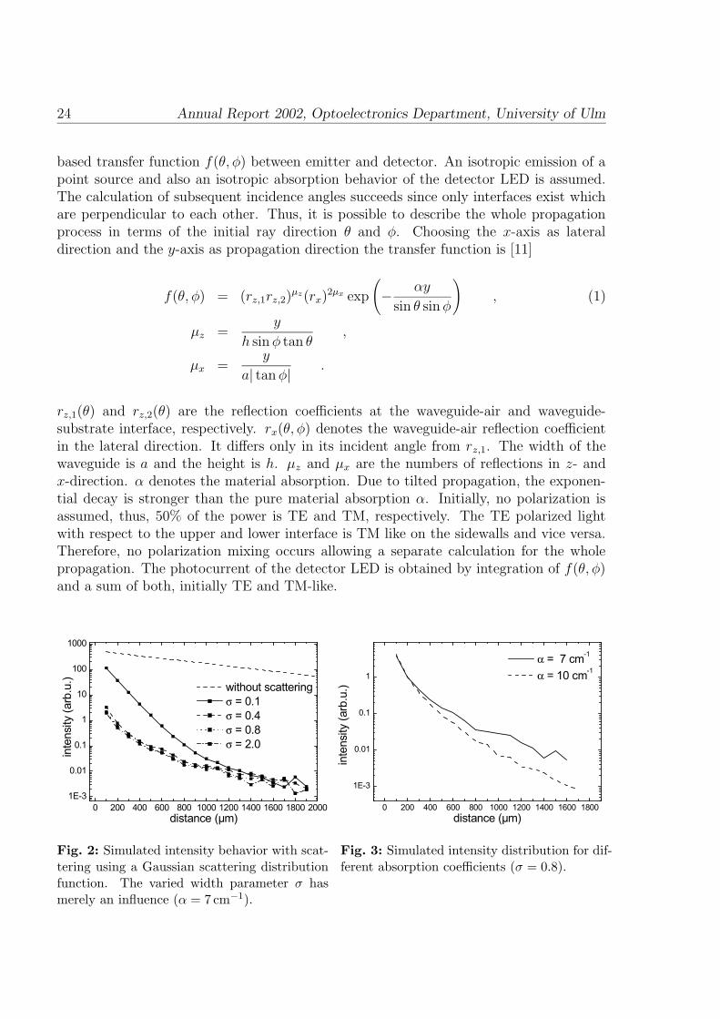
αα
Fig. 1: Calculated intensity decay in a single layer film on a substrate layer without scattering.Curve for α = 20 cm−1 , refractive index of film nf = 2.5 and substrate ns = 1.75. The widthof the film a is 100 µm, the height h is 2.5 µm. The waveguide dispersion increases the observedabsorption, thus, a linear fit yields to α = 27 cm−1.
intensity decay within the waveguide can be obtained. Thus, the method does not allow aspectrally resolved behavior. Also, a spectral weighting due to the sensitivity of the LEDdetector has to be accepted. Another etching step is employed to isolate the emitter,waveguide, and detector by a 4µm wide groove and to uncover the buried side of thep–n-junction. The comparably large groove will introduce coupling losses between theemitter and the waveguide, however, because of the large lateral dimension, enough lightremains to obtain a sufficient photocurrent. In turn, the waveguide is multi-mode anddispersion has to be considered. However, coupling light of a LED into a single modewaveguide is inefficient, so a multimode waveguide has to be used for this kind of experi-ment anyway. Lateral guiding is guaranteed by the index change of the semiconductor-airinterface. In perpendicular direction the semiconductor-air and the GaN-sapphire inter-faces cause sufficient reflections within GaN-based samples. To obtain a waveguide inAlGaInP-structures, a thick AlAs layer between AlGaInP and GaAs-substrate is used.
2.2 Theoretical considerations
In order to explain the observed intensity distribution, an analytical model is desirable.However, the complex layer structure of light emitting diodes impedes a practical descrip-tion. Therefore, the basic effects are studied at a two layer model consisting of a waveguideon the top of a substrate, whereas for the evaluation of the absorption coefficient, a raytracer is used.
Without scattering, the intensity distribution can be calculated by an analytically ray-
24 Annual Report 2002, Optoelectronics Department, University of Ulm
based transfer function f(θ, φ) between emitter and detector. An isotropic emission of apoint source and also an isotropic absorption behavior of the detector LED is assumed.The calculation of subsequent incidence angles succeeds since only interfaces exist whichare perpendicular to each other. Thus, it is possible to describe the whole propagationprocess in terms of the initial ray direction θ and φ. Choosing the x-axis as lateraldirection and the y-axis as propagation direction the transfer function is [11]
f(θ, φ) = (rz,1rz,2)µz(rx)
2µx exp
(
− αy
sin θ sinφ
)
, (1)
µz =y
h sinφ tan θ,
µx =y
a| tanφ| .
rz,1(θ) and rz,2(θ) are the reflection coefficients at the waveguide-air and waveguide-substrate interface, respectively. rx(θ, φ) denotes the waveguide-air reflection coefficientin the lateral direction. It differs only in its incident angle from rz,1. The width of thewaveguide is a and the height is h. µz and µx are the numbers of reflections in z- andx-direction. α denotes the material absorption. Due to tilted propagation, the exponen-tial decay is stronger than the pure material absorption α. Initially, no polarization isassumed, thus, 50% of the power is TE and TM, respectively. The TE polarized lightwith respect to the upper and lower interface is TM like on the sidewalls and vice versa.Therefore, no polarization mixing occurs allowing a separate calculation for the wholepropagation. The photocurrent of the detector LED is obtained by integration of f(θ, φ)and a sum of both, initially TE and TM-like.
σσσσ
Fig. 2: Simulated intensity behavior with scat-tering using a Gaussian scattering distributionfunction. The varied width parameter σ hasmerely an influence (α = 7 cm−1).
αα
Fig. 3: Simulated intensity distribution for dif-ferent absorption coefficients (σ = 0.8).

Absorption of Guided Modes in Light-Emitting Diodes 25
Exemplarily, we calculated the intensity distribution function for a nitride-based samplewhich is depicted in Fig. 1. Within the first 40µm losses from leaky modes dominatethe intensity decay. Then, the behavior is almost exponential. As expected, the observedintensity decay is larger than the material absorption caused by waveguide dispersionwhich is accounted by sin θ sinφ in the exponential term in Eqn. 1. Between zero and40µm emission from leaky modes dominates the intensity decay. Summarizing the model,the presence of waveguide dispersion increases the intensity decay but the behavior is stillexponential and the emission from leaky modes is on a comparable small scale.
Next, scattering is considered. In our model, the direction of reflected light is modifiedaccording to a scattering distribution function. Since this statistical approach requiresa complete calculation of the propagation trajectory for each ray, a ray tracer has beenemployed. For the simulation, the same geometry is taken. Regarding the nitride samplesgrown on sapphire, two possible scattering regions exist, the buffer layer and, if unpolished,the substrate-side sapphire-air interface. However, we investigate in this work only theinfluence of the buffer layer (see below). Therefore, back reflections from the substrate-airinterface are avoided in the simulation model by a strong absorbing layer. A Gaussian dis-tribution function with width σ is applied at all surfaces of the waveguide. Although bulkscattering would represent the physical occurrence better, the exponentially increasingsimulation effort caused by an additional layer forces a trade off. However, the expecteddifferences are small.
Fig. 2 depicts the obtained intensity distribution. The presence of scattering causes abowing of the intensity distribution curve with increasing σ. If σ is chosen between 0.4and 2.0, the intensity behavior gets more and more independent of the absolute value ofσ as can be seen from the simulation curves. In contrast, a strong dependence on theabsorption coefficient remains as shown in Fig. 3.
3. Experimental
3.1 InGaN-sapphire based LED samples
The measurements are done using a HP4145 semiconductor parameter analyzer. I–Vcurves of the detector LED structures are shown in Fig. 4 with and without photocurrent.For large backward voltages, the devices exhibit a parallel resistance which is attributedto etching induced surface defects. However, between 1.7 V and −5 V, the current isdominated by the noise limit of voltage source. Switching on the light emitter by applyinga current of 10 mA causes a significant increase in current of the detector LED. To getrid of the parasitic leakage current and the noise current, a subtraction of both curvesis carried out. The result is illustrated in Fig. 5. However, for low currents and largereverse biases, an influence of leakage current remains. Furthermore, the photocurrent isa function of voltage, since a band alignment due to the quantum confined Stark effectoccurs. Thus, the photocurrent as function of distance is evaluated by a cross section atV = 0.

26 Annual Report 2002, Optoelectronics Department, University of Ulm
Fig. 4: I–V -curve of a detector LED with andwithout photocurrent.
Fig. 5: Sample 1: Measured photocurrent independance of distance.
Two samples are investigated which have been grown using the same growth parameters.The simplified layer structure is as follows. On a 330µm thick sapphire substrate anucleation is performed and a buffer layer is grown. After that, a 1.5µm thick silicondoped layer follows. The next layers build a fivefold multi-quantum well (MQW) structurefollowed by an AlGaN barrier consisting of approximately 10% aluminum. The top layeris magnesium doped gallium nitride. The emission wavelength was adjusted by the growthtime, thus a shifting of the ground level of the wells is chosen instead of varying the indiumcontent. The thickness of the complete epitaxial stack is 2.4µm. Sample 1 exhibits anemission wavelength of 441 nm and FWHM of 20 nm, whereas the emission wavelength ofSample 2 is 415 nm with FWHM of 15.4 nm. Both devices show on wafer output powerslarger than 1 mW at a current of 20 mA. The intensity behavior is depicted in Fig. 6.Best agreement with simulation is achieved by an absorption coefficient of α = 7 cm−1
and σ = 0.8 for both samples.
In Section 2.2 we did not preclude an influence of the rough substrate-air interface, thisis taken up by means of a further experiment. If significant back reflection was present,an increase of substrate thickness would decrease the parasitic effect on the intensitydistribution. Therefore, a 50 mm thick sapphire cylinder, 50 mm in diameter was putunder the sample and to overcome the problem of interface roughness, diiodmethane wasused as index matching fluid to achieve good optical coupling. The obtained intensitydistribution is shown in Fig. 7 which only differs slightly from the measurement before.Thus, it is concluded that the substrate back reflection is not dominating the intensitycurves.
3.2 AlGaInP based LED samples
The evaluation of photocurrent is accomplished in the same manner as for nitride samples.Fig. 8 depicts the photocurrent in dependance of voltage. The emitting LED structure was

Absorption of Guided Modes in Light-Emitting Diodes 27
α
Fig. 6: Photocurrent as function of distance.Sample 1: InGaN-LED with emission wave-length of λ = 441 nm and FWHM of 20 nm.Sample 2: InGaN-LED with emission wave-length of λ = 415 nm and FWHM of 15.4 nm.Both samples show on wafer output powers ex-ceeding 1 mW at I = 20 mA. The intensity dis-tributions agree well with the simulation curvefor α = 7 cm−1.
Fig. 7: Sample 2: If a significant fractionof detected light is caused by substrate back-reflection, it will be reduced by a larger prop-agation distance due to a decrease in solid an-gle (r−2-law of propagation). However, themeasurement carried out on a large sapphirecylinder (I = 5 mA) and without are alike(I = 10mA). Thus, the intensity distribution isnot affected by back reflection from the roughsapphire-air interface.
driven at a current of 5 mA. Compared with the nitride samples, no voltage dependanceis observed. Fig. 9 shows the photocurrent as function of distance. In contrast tonitride samples, no significant scattering is present, therefore, the evaluation of absorptioncoefficient is done by an exponential fit which leads to α = 30 cm−1 disregarding waveguidedispersion. Still unclear is the influence of the spectral response of the detecting LEDstructure on the results. Therefore, the detector LED is replaced by a spectrometer.To maintain same coupling efficiency during the measurement, another waveguide wasdesigned providing contacts on top with a distance of 250µm. The waveguide was cleavedand the spectra of the emitted light through the facet have been measured. Regardingagain Fig. 9, it is obvious that an evaluation of the absorption coefficient should becarried out for distances larger than 1000µm, however, a measurement of spectra for LEDstructures in that region was not possible due to the small amount of emitted power.

28 Annual Report 2002, Optoelectronics Department, University of Ulm
Fig. 8: Sample 3: Measured photocurrent independance of distance for the AlGaInP-basedLED.
α
Fig. 9: Sample 3: AlGaInP-LED with emis-sion wavelength of λ = 650 nm. Data is fit byan exponential law, α = 30 cm−1. It is foundthat absorption is much larger in the AlGaInP-based LED structure than in the nitride-basedone (Sample 2, λ = 415 nm).
Fig. 10: Sample 3: Spectrally resolved ab-sorption determined by subtraction of spectraof two adjacent LED structures as function oftheir mean distance to the facet.
Fig. 11: Sample 3: Comparison of intensity de-cay using both, the photocurrent and averagedspectra.

Absorption of Guided Modes in Light-Emitting Diodes 29
The spectral absorption curves depicted in Fig. 10 are calculated by subtraction of twosubsequent spectra at each case. Determined values are larger than the material absorp-tion because of influence of waveguide dispersion. When employing a spectral averaging,a comparison with the photocurrent measurement is possible which is depicted in Fig.11. Both measurement methods agree well with each other indicating that the spectralsensitivity of the detector LED structure plays a minor role.
4. Conclusion
We present a technique to determine the absorption of lateral guided modes in lightemitting diodes. Absorption of InGaN-on-sapphire-based and AlGaInP-based structuresis determined by comparison with ray tracing simulation curves. For the nitride samples,it is found that the lateral intensity distribution is governed by buffer scattering. A goodagreement of measured photocurrent is found which enables a reliable determination ofabsorption. For both nitride samples with emission wavelengths of 415 nm and 441 nm,an absorption coefficient of 7 cm independent of the emission wavelength is determined.The investigated AlGaInP-based sample exhibits an absorption of α = 30 cm−1 at 650 nmemission wavelength which is significantly larger than the absorption in both nitride-basedsamples.
References
[1] M. Rattier, H. Benisty, R.P. Stanely, J.F. Carlin, R. Houdre, U. Oesterle, C.J.M.Smith, C. Weisbuch, and T.F. Krauss, “Towards Ultrahigh-Efficiency AluminiumOxide Microcavity Light-Emitting Diodes: Guided Mode Extraction by PhotonicCrystals,” IEEE J. Select. Topics Quantum Electron., vol. 8, no. 2, pp. 238–247,2002.
[2] R. Windisch, C. Rooman, B. Dutta, A. Knoblauch, G. Borghs, G.H. Dohler, and P.Heremans, “Light-Extraction Mechanisms in High-Efficiency Surface-Textured Light-Emitting Diodes,” IEEE J. Select. Topics Quantum Electron., vol. 8, no. 2, pp. 248–254, 2002.
[3] M.O. Holcomb, M.R. Krames, G.E. Hofler, C. Carter-Coman, E. Chen, P. Gril-lot, K. Park, N.F. Gardner, J.-W. Huang, J. Posselt, D. Collins, S.A. Stockman,G.M. Craford, F.A. Kish, I-H. Tan, T.S. Tan, C.P. Kocot, and M. Hueschen, “Highpower Truncated-Inverted Pyramid (AlxGa1−x)0.5In0.5P Light-Emitting Diodes,”Proc. SPIE, vol. 3938, pp. 77–81, 2000.
[4] F.A. Kish, F.M. Steranka, D.C. DeFevere, D.A. Vanderwater, K.G. Park, C.P.Kuo, T.D. Osentowski, M.J. Peanasky, J.G. Yu, R.M. Fletcher, D.A. Steigerwald,M.G. Craford, and V.M. Robbins, “Very high-efficiency semiconductor wafer-bonded

30 Annual Report 2002, Optoelectronics Department, University of Ulm
transparent-substrate (AlxGa1−x)0.5In0.5P/GaP light-emitting diodes,” Appl. Phys.Lett., vol. 64, no. 21, pp. 2839–2841, 1994.
[5] S.S. Schad, M. Scherer, M. Seyboth, and V. Schwegler, “Extraction efficiency of GaNbased LEDs,” phys. stat. sol. (a), vol. 188, pp. 127–130, 2001.
[6] J.F. Muth, J.H. Lee, I.K. Shmagin, R.M. Kolbas, H.C. Casey, B.P. Keller, U.K.Mishra, and S.P. DenBaars, “Absorption coefficient, energy gap, exciton binding en-ergy, and recombination lifetime of GaN obtained from transmission measurements,”Appl. Phys. Lett., vol. 71, no. 18, pp. 2572–2574, 1997.
[7] G. Yu, G. Wang, H. Ishikawa, M. Umeno, T. Soga, T. Egawa, J. Watanabe, andT. Jimbo, “Optical properties of wurzite structure GaN on sapphire around thefundamental absorption edge (0.78-4.77) eV by spectroscopic ellipsometry and theoptical transmission method,” Appl. Phys. Lett., vol. 70, no. 24, pp. 3209–3211, 1997.
[8] G.Y. Zaho, H. Ishikawa, T. Egawa, T. Jimbo, and M. Umeno, “Optical Absorptionand Photoluminescence Studies of n-type GaN,” Jap. J. Appl. Phys., vol. 38, no. 2,pp. 993–995, 1999.
[9] D. Brunner, H. Angerer, E. Bustarret, F. Freudenberg, R. Hopler, R. Dimitrov,O. Ambacher, and M. Stutzmann, “Optical constants of epitaxial AlGaN films andtheir Photoluminescence Studies of n-type GaN ,” Appl. Phys. Lett., vol. 82, no. 10,pp. 5090–5096, 1997.
[10] O. Ambacher, D. Brunner, R. Dimitrov, M. Stutzmann, A. Sohmer, and F. Scholz,“Absorption of InGaN Single Quantum Wells Determined by Photothermal Deflec-tion Spectroscopy,” Jap. J. Appl. Phys., vol. 37, no. 1, pp. 745–752, 1998.
[11] S.S. Schad, B. Neubert, M. Seyboth, F. Habel, C. Eichler, M. Scherer, P. Unger, W.Schmid, C. Karnutsch, and K.P. Streubel, “Absorption of guided modes in light emit-ting diodes,” in Light-Emitting Diodes: Research, Manufacturing, and Applications,F. Schubert, SPIE Proc. 4996 , Jan 2003.

Basics of MBE 31
Basics of Molecular Beam
Epitaxy (MBE)
Fernando Rinaldi
A brief introduction to the MBE technique is presented with main attention to the el-emental source MBE. A discussion on the effusion cell as beam source is shortly givenstarting from ideal cases to real cells homogeneity problems. A short review regardingthe thermodynamic approach to the MBE is pointed out. Focusing on the possibility that,despite the fact that MBE processes occur under strong nonequilibrium conditions, for theIII/V elements, a thermodynamic approach can be used on the basis of equations for massaction in combination with the equations describing the conservation of the mass of theinteracting elements.
1. Introduction
Molecular beam epitaxy is a technique for epitaxial growth via the interaction of oneor several molecular or atomic beams that occurs on a surface of a heated crystallinesubstrate. In Fig. 1 a scheme of a typical MBE system is shown. The solid sourcesmaterials are placed in evaporation cells to provide an angular distribution of atoms ormolecules in a beam. The substrate is heated to the necessary temperature and, whenneeded, continuously rotated to improve the growth homogeneity.According to Fig. 2, the molecular beam condition that the mean free path λ of theparticles should be larger than the geometrical size of the chamber is easily fulfilled if thetotal pressure does not exceed 10−5 Torr. Also, the condition for growing a sufficientlyclean epilayer must be satisfied, e.g. requiring for the monolayer deposition times of thebeams tb and the background residual vapor tres the relation tres < 10−5 tb. For a typicalgallium flux Γ of 1019 atoms m−2s−1 and for a growth rate in the order of 1µm/h, theconclusion is that pres ≤ 10−11 Torr. Considering that the sticking coefficient of gallium onGaAs atoms in normal operating conditions is approximately unity and that the stickingcoefficient of most of the typical residual gas species is much less than 1, the conditionabove results to be not so strict, nevertheless ultra high vacuum (UHV) is required.Thus, UHV is the essential environment for MBE. Therefore, the rate of gas evolutionfrom the materials in the chamber has to be as low as possible. So pyrolytic boron nitride(PBN) is chosen for the crucibles which gives low rate of gas evolution and chemicalstability up to 1400 C, molybdenum and tantalum are widely used for the shutters, theheaters and other components, and only ultrapure materials are used as source. To reachUHV, a bakeout of the whole chamber at approximately 200 C for 24 h is required any

32 Annual Report 2002, Optoelectronics Department, University of Ulm
time after having vented the system for maintenance. A cryogenic screening around thesubstrate minimizes spurious fluxes of atoms and molecules from the walls of the chamber.Despite this big technological problems, MBE systems permit the control of composition
Fig. 1: A typical MBE system.
10−10 10−810−6 10−4 10−2 100
Pressure (Torr)
10−2
100
102
104
106
108
Mea
n fr
ee p
ath
(cm
)
Fig. 2: Mean free path for nitrogenmolecules at 300K.
and doping of the growing structure at monolayer level by changing the nature of theincoming beam just by opening and closing mechanical shutters. The operation time ofa shutter of approximately 0.1 s is normally much shorter than the time needed to growone monolayer (typically 1–5 s). Careful variation of the temperatures of the cells viaPID controllers permits the control of the intensity of the flux of every component ordopant of better than 1 %. The UHV environment of the system is also ideal for many in-situ characterization tools, like the RHEED (reflection high energy electron diffraction).The oscillation of the RHEED signal exactly corresponds to the time needed to grow amonolayer and the diffraction pattern on the RHEED window gives direct indication overthe state of the surface as can be seen in Fig. 3.
Inte
nsi
ty
time
Fig. 3: RHEED oscillations.

Basics of MBE 33
2. Effusion Cells
The effusion cells used in MBE systems exploit the evaporation process of condensedmaterials as molecular flux source in vacuum. The understanding of the properties of realeffusion cells is complicated and not straightforward, so easier models are needed and justthe main complications are subsequently added.In a closed enclosure, for pure substances, an equilibrium is estabilished between thegas and the condensed phase. Such systems have only one degree of freedom f , thatmeans that the pressure peq is a function of the temperature T and can be approximatelyexpressed by the Clapeyron equation [1]
peq(T ) = A exp(
−∆H
kBT
)
. (1)
Where in (1) ∆H is the evaporation enthalpy and kB the Boltzmann constant. Under thisequilibrium condition, we observe that when the peq is very low, it is possible to treat theincoming and the outcoming flux independently. A close look to the fluxes of particleshaving a mass m on the condensed phase surface shows that the maximum value for theevaporated flux Γm is
Γm =peq√
2πmkBT. (2)
This assumes that each molecule from the gas phase is always trapped by the surfaceand an equal opposite flux of material must leave the condensed phase to maintain theequilibrium pressure. Considering now that the impinging beam is partially reflected andonly a fraction a is accommodate on the surface, the complete expression for the fluxleaving the surface can be easily found as
Γ = aΓm. (3)
The factor a is dependent on the microscopic status of the surface and is strongly un-predictable and because of (3) the flux of material. The Knudsen evaporating methodovercome this problem providing a molecular beam that is independent of a. An idealKnudsen cell is composed of a large enclosure were the condensed material is in thermo-dynamic equilibrium with the gas phase and of an orifice so small that the equilibriumpressure peq is not perturbed. The orifice geometry has to fulfill two additional conditions,one for the diameter d, that fullfils d λ at peq and one for its wall thickness L, assumedto be vanishingly thin. Under these conditions, the orifice is a surface with an evaporantpressure peq and has not the ability to reflect any of the incoming molecules resulting ina = 1 and the number of molecules per time unit of the created beam is A Γm, where Ais the orifice area.The ideal Knudsen cell exhibits an angular distribution of the evaporated particles thatfollows a cosine law, where the angle θ is referred to the normal to A.
dΓθ
dΩ=
Γm
πcos θ, (4)

34 Annual Report 2002, Optoelectronics Department, University of Ulm
so that the flux at distances much bigger than the orifice dimensions is proportional tocos θ. Using Clausing’s model [2] for the conductance of a molecular flow in a cylindricaltube, Dayton has studied the deviation from ideality given when L/d is not longer 0. Inthis calculations a model is necessary to describe the interaction of the molecules withthe orifice walls. Random reflection is the simplest approach, but also more complicatedones are possible involving also temporary adsorption and surface diffusion [3]. However,an estimation of a for the surface of the condensed material is not required. WhenL/d increases, the beam is more focused on the normal direction and for L/d = 1 thedeviation from the cosine law is relevant. These models are important tools to measure peq
and so thermodynamic quantities related with (1). When it is not possible to consider theenclosure as infinitely large and when it is therefore important to consider the influencesof the main body of the cell, the value of the a coefficient is needed [4]. This is also thecase of cylindrical and conical cells, that are widely used in MBE systems, there is nothermodynamic equilibrium between condensed and gas phase and therefore the value ofa is necessary to calculate the emerging flux. Nevertheless, assuming for a a homogeneousdistribution on the condensed phase material surface, it is possible to estimate the shapeof the outcoming vapour beam using all the modelling discussed before. Many variables
Fig. 4: Example of the geometrical config-uration for a conical effusion cell.
T
x0.5
GaAs(s)
Ga(l)
GaAs(s)GaAs(s)
As(s)
liquid
1
2
Fig. 5: Simplified phase diagram (T–x sec-tion) for GaAs. (s) is the solid and (l) isliquid phase. A gas phase is always present.
are involved in this problem, like shown in Fig. 4. For example, very often the sourcematerial is in liquid form (Ga, Al, In) and so an additional angle α is required to set upthe geometry of the system. Some materials wet the crucible surface (e.g. aluminum inPBN crucibles), so other variables are needed to specify the position of the evaporatingsurface. A complex work of optimization is therefore necessary in relation to the factthat in a MBE system many cells must operate and for each one a suitable geometricalconfiguration cell substrate must be properly chosen. Control and homogeneity of the cellstemperature are crucial, because of the strong dependence of the flux on temperature.W-Re thermocouples are used for the chemical stability at high temperatures and for thevery low outgassing rate. Tantalum heater elements and radiative shields are chosen forthe excellent refractory properties. These elements are often self-supporting preventingthe use of material that does not have such low rate of gas evolution. Great care is

Basics of MBE 35
also needed to decrease the temperature difference between heater and crucible. This isnecessary to avoid very high temperature outgassing from tantalum, and to reduce thedissipated heat which causes possible uncontrolled outgassing from other parts of thevacuum chamber.
3. Thermodynamic Approach
In the past there was a lot of controversy concerning the possibility of applying thermody-namics to the growth processes in MBE. In the 1980s, MBE was developing experimentallyvery successfully, and most of the problems particularly regarding AlGaAs and InGaAlAsmaterials were solved empirically. In recent years, the need for MBE grow with newermaterials revealed the importance of a closer theoretical modeling of the growth processes.In the case of MBE, it seems that the system cannot be described by a thermodynamicrepresentation, because the different parts like sources, substrate, and walls are at differ-ent temperatures. However, it is possible to assume that the temperature of the systemis the temperature of the substrate if the thermalization time is much shorter than thetime required to grow a monolayer. So we consider an equilibrium state in which the par-tial pressures are the ones relative to fluxes of atoms or molecules leaving the substratessurface at its temperature.The validity of this assumption is confirmed by two facts. First that the fluxes of atomsor molecules leaving the substrate have its temperature irrespective of the temperatureof fluxes arriving at the surface. Second, the nature of the arsenic molecules, e.g. in theGaAs system, leaving the substrate is independent of the nature of the arsenic moleculesreaching the surface. In this case, we have to consider the following reaction with theassociated mass action equation [5]
2As2(g) As4(g) and p2As2
p−1As4
= 3.98 · 108 exp(
−2.35
kBT
)
, (5)
where the pressures are measured in atmospheres and kBT in eV. The dimeric fractionof arsenic molecules leaving the substrate exactly follows the temperature behaviour pre-dicted by (5) [6]. Starting by these assumptions it is possible to model the basic behavior ofthe III/V binary compounds in MBE conditions. For a binary compound, a phase diagramlike the one sketched in Fig. 5 must be considered. In the region labeled with 1 GaAs(s)is present in equilibrium with Ga(g) and As2(g) and As4(g)(with just a small deviation,exaggerated in the figure, from the Ga0.5As0.5 stoichiometry possible via point defect, butalways much smaller than 10−4 even at high temperatures). Using the Gibbs’ Phase Rulef = c − p + 2 [7] that relates the number of components c and the number of differentphases p to the number of degrees of freedom f , it is easy to recognize that in the region 1of the phase diagram f = 2. So temperature and pressure are independent. In the region2, liquid gallium is present and therefore f = 1 as 3 phases are present. Hence a functionp = p(T ) exists. In the region 1, the reactions between the components are
GaAs(s) Ga(g) +1
2As2(g) and 2As2(g) As4(g). (6)

36 Annual Report 2002, Optoelectronics Department, University of Ulm
The mass action equation is
pGa p12
As2= KGaAs = 2.73 · 1011 exp
(
−4.72
kBT
)
. (7)
Under normal MBE growth conditions, when T > 450 C, it is possible to neglect thepAs4 contribution to the total pressure. Therefore the total pressure is given by
pT = pGa + pAs2 =KGaAs
p12
As2
+ pAs2 . (8)
The gallium pressure is maximum on the left side of the diagram, where it approximatelycorresponds to the gallium pressure on pure liquid gallium, moving to the right, becauseof (7), this partial pressure will decrease while the arsenic pressure is increasing. For somerange in temperature, the pressure shows a minimum for a suitable stoichiometry of thesolid phase. This is the condition that has to be applied to find the flux in free sublimation,i.e. sublimation in vacuum. The reason for the minimum condition is very general [8].In a compound AxB1−x, the pressure is the sum of the pressures of its components. Ifthe partial pressure of the component B is bigger than the one of the component A, thecomposition of the condensed phase will be enriched with A, moving the system to a lowerpartial pressure. If a minimum for a certain x exists, this will be asymptotically reached.In this point the sublimation is congruent. In our case the equation for a minimum of thepressure is
dpT
dpAs2
=dpT
dpGa
= 0. (9)
Solving this with the (8) will bring the result
pGa = 2 pAs2 = (2K2GaAs)
13 . (10)
This corresponds to congruent sublimation of GaAs. When the temperature increasesover a certain temperature Tmax, the pressure of the more volatile component, in thiscase arsenic, increases faster and there will be no minimum in the region 1. Under thiscondition, a liquid gallium phase is created. The temperature Tmax is called “temperatureof maximum sublimation”. Tmax is calculated imposing pGa from (10) equal to the valueof the gallium pressure over the liquid gallium
pLGa = 2.88 · 105 exp
(
−2.74
kBT
)
. (11)
The value of Tmax is approximately 630 C. The free sublimation rate is so given by
v = −VpGa√
2πmGa kBT, (12)
where pGa is defined by (9) and V is the volume occupied by a pair of gallium and arsenicatoms in GaAs. When an external As2 flux is supplied, so that pext
As2 pAs2 , for the (7)
we will obtain a reduced Ga evaporated flux
predGa =
KGaAs
(pextAs2
)12
. (13)

Basics of MBE 37
Thereby a suppression of the sublimation occurs. The rate of evaporation inversely pro-portional to the square root of the arsenic flux to the substrate is experimentally observedin MBE systems. For an external As4 flux in (13), pext
As2must be exchanged with 2 pext
As2.
It is important to emphasize that in the previous calculations we have used the fact thatthe sticking coefficient of gallium on GaAs is ≈ 1, because the outcoming flux, and so therelated pressure, is always given by (3).When an external gallium flux is added the growth rate can be expressed by
v = −VpGa − pext
Ga√2πmGa kBT
. (14)
Just considering that the arsenic flux is always much bigger than the one of gallium,neglecting the fraction of arsenic that will take part in the growth process, and consideringalways the condition pAs2 pAs4 , for the growth rate we get
v = C
pextGa −
KGaAs
(pextAs2
)12
. (15)
Also the temperature dependence implicit in (15) was experimentally found [9]. So forthe typical pext
As2with a value of 10−6 − 10−4 Torr which is used, the growth rate is mainly
controlled by the gallium flux. A solid arsenic phase is never formed in MBE systembecause the typical arsenic pressure would be for this temperature, T> 500 C, in Torrrange. The excess arsenic flux fixes a point in the phase diagram and so determines thetype and concentration of point defects. This considerations are valid for many III/Vcompounds [10].
Compounds KIII/V Tmax( C)
AlAs 1.63 · 1010 exp(
− 5.39kBT
)
902
GaAs 2.73 · 1011 exp(
− 4.72kBT
)
630
GaP 2.26 · 1011 exp(
− 4.71kBT
)
571
InAs 7.76 · 1011 exp(
− 4.34kBT
)
508
InP 8.34 · 1011 exp(
− 4.02kBT
)
268
For each compound equations like (11) can be used to calculate the Tmax. Extremely inter-esting is an overview on the ternary compounds. AlxGa1−xAs, GaxIn1−xAs, AlxIn1−xAswere successfully analyzed. The problem in a ternal compound is the estimation of theactivities coefficient γ that take the nonideal nature of the alloy into account. AlxGa1−xAsis a special case having γGaAs = γAlAs = 1. In other cases, e.g. GaAsxP1−x we can writethe following equations
pGa p12
As2= γGaAsKGaAsx and pGa p
12
P2= γGaPKGaP(1 − x) (16)

38 Annual Report 2002, Optoelectronics Department, University of Ulm
together with the (5) and another mass action equation for the reaction 2P2(g) P4(g).Considering that again the dimers are the dominating species, for T> 500 C, and ne-glecting the amount of group-V elements that take part in the growth process we can findfor the resulting final composition of GaAsxP1−x
x =1
(
γGaPKGaP
γGaAsKGaAs
)
(
pextP2
pextAs2
)12
+ 1
(17)
Even neglecting the influence of the activity coefficients in (17), a good qualitative agree-ment can be found with the experimental data [11].
References
[1] R.A. Swalin, Thermodynamics of solids. New York: John Wiley & Sons, 1972.
[2] J.F. O’Hanlon, A User’s Guide to Vacuum Technology. New York: John Wiley &Sons, 1989.
[3] W.L. Winterbottom and J.P. Hirth, “Diffusional contribution to the total flow froma Knudsen cell,” J. Chem. Phys., vol. 37, no. 4, pp. 784–793, 1962.
[4] K. Motzfeldt, “The thermal decomposition of sodium carbonate by the effusionmethod,” J. Phys. Chem., vol. 59, pp. 139–147, 1955.
[5] D.T.J. Hurle, “Revised calculation of point defect equilibria and non-stoichiometryin gallium arsenide,” J. Phys. Chem. Solids, vol. 40, pp. 613–626, 1979.
[6] C.T. Foxon, J.A. Harvey, and B.A. Joyce, “The evaporation of GaAs under equilib-rium and non-equilibrium condition using a modulated beam technique,” J. Phys.Chem. Solids, vol. 34, no. 10, pp. 1693–1701, 1973.
[7] H.A.J. Oonk, Phase Theory, vol. 3. Amsterdam, Netherlands: Elsevier ScientificPublishing Company, 1981.
[8] F.A. Kroger, The Chemistry of Imperfect Crystals, vol. 1. Amsterdam, Netherlands:North Holland Publishing Company, 1973.
[9] J.M. van Hove and P.I. Cohen, “Mass action control of AlGaAs and GaAs growth inmolecular beam epitaxy,” Appl. Phys. Lett., vol. 47, no. 7, pp. 726–728, 1985.
[10] P.S. Kop’ev and N.N. Ledentsov, “Molecular beam epitaxy of heterostructures madeof III/V compounds,” Sov. Phys. Semicond., vol. 22, no. 10, pp. 1093–1101, 1988.
[11] S. Gonda and Y. Matsushima, “Molecular beam epitaxy of GaP and GaAsP,” Jap.J. Appl. Phys., vol. 15, no. 11, pp. 2093–2101, 1976.
Optical Coatings for Laser Facets 39
Optical Coatings for Laser Facets
Fabricated by Reactive Ion-Beam Sputter Deposition
Steffen Lorch
Reactive ion-beam sputter deposition is the preferred method to fabricate stoichiometricand dense layers for optical coatings with very low optical absorption. The refractive in-dices and thicknesses of such single- or multilayers can be optimized to get the required re-flectivities for antireflection/high-reflection coatings on laser facets or antireflection coat-ings lower than 10−4 for laser amplifiers. Lasers can be coated after cleaving or on-wafercoating can be done on dry-etched laser facets. These AR/HR coatings can be charac-terized by using the threshold shift method or from the ratio of the emitted light of bothfacets.
1. Introduction
Optical coatings are used for adjustment of facet reflectivity R and for passivation of semi-conductor lasers. For conventional semiconductor lasers, an antireflection/high-reflectioncoating (AR/HR with e. g. R = 10 %/90 %) is used. However, for laser amplifiers, antire-flection (AR) coatings with very low reflectivity (R ≤ 10−4) are required. Due to the highintensity on the output facet, the coating becomes hot and can be destroyed by catas-trophic optical mirror damage (COMD) processes. The power at which this occurs canbe increased by using coatings with a low optical absorption. This can be realized withvery dense and stoichiometric oxide layers. The best method to fabricate such opticalcoatings is reactive ion-beam sputter (RIBS) deposition with an assisted ion beam. [1, 2]describes why such a deposition method is the preferred method for optical coatings.
2. Ion-Beam Sputter Deposition System
Laser facets have been coated with an ion-beam sputter (IBS) deposition system. Cleavedlasers can be loaded in a laser-bar holder and using two deposition steps, the AR and theHR coating are deposited. Also on-wafer coating is possible if the facets are dry etchedwith for example a CAIBE system.

40 Annual Report 2002, Optoelectronics Department, University of Ulm
2.1 Design of the coatings
Firstly, the refractive index of the deposited material must be known. For that a thicklayer (about 1µm) of the material is coated on a microscope slide. The reflection andtransmission is measured over the wavelength. With a simulation program (EssentialMacleod [3]) both the refractive index and extinction coefficient can be calculated fromthese values. The principle for this calculation is described in [4, 5]. With this simulationprogram the required thicknesses of the layers with the given refractive indices of the us-able materials can be simulated for the desired reflectivities. Additionally, the depositionrates for the different materials must be known. For that a test layer is deposited ontoa silicon substrate and the thickness can be measured with an ellipsometer. With thedeposition rates and required layer thicknesses now known the coatings can be deposited.
2.2 The IBS deposition system
Fig. 1: The ion-beam sputter depositionsystem.
2O3Al
Ar+
Ar
neutralizer
holderSubstrate
ion−beam sourceKaufman
Filament
2 targetsSi /
Load lock
Fig. 2: Schematic diagram of the ion-beamsputter deposition system.
The ion-beam sputter deposition system used is shown in Fig. 1. The system has a loadlock for a large throughput. The ion-beam is generated with a Kaufman ion-beam source(the functionality of such a source is described in [6]). The ion-beam current is an im-portant parameter for the deposition and is constant during the deposition process. Twodifferent targets can be used, Al2O3 and Si. The geometry in the process chamber can bechanged; the distance between ion-beam source and target, the target angle, the distancebetween target and substrate, and the substrate angle. Additionally the substrate ma-nipulator can rotate for an improved homogeneity. A schematic of the system is shownin Fig. 2.
2.3 AR/HR coating on cleaved lasers
The facets of a laser should have two different reflectivities [7]. The output facet shouldhave an antireflection coating with a reflectivity of 5 % to 10 % and the rear facet a high-

Optical Coatings for Laser Facets 41
reflection coating with a reflectivity of 80 % to 95 %. In order to apply the coatings onthe facets, the lasers are first cleaved and loaded in a laser bar holder. After mountingthe holder on the substrate manipulator one side can be coated. After that, the holdermust be turned and remounted to deposite the other facet.
In the case for such a AR/HR coating, the power of the outgoing light on the AR-coatingside is much higher than the light going out at the HR-coating side. The ratio of thesetwo output powers can be calculated using [8]
PAR
PHR
=
√RHR(1 −RAR)√RAR(1 −RHR)
. (1)
Fig. 3: Refractive index layout of a 5-layerhigh-reflection coating.
Fig. 4: Ratio of the output power of bothfacets over normalized current.
For an AR coating, a single layer of Al2O3 can be used. For the HR coating, five layersmust be used. The refractive index layout for such a 5-layer coating is shown in Fig. 3. Thecharacterization of the coating can be done by dividing the L–I curve of the AR-coatingside by the L–I curve of the HR-coating side. In Fig. 4, this ratio is shown normalized tothe threshold current for a laser with an AR/HR coating with 5 %/94 %. It can be seen,that above the threshold current the AR/HR ratio is constant at about 40. But accordingto Eqn. (1) for the given reflectivities the ratio should be higher at 72. The reason forthat deviation is not yet known.
2.4 On-wafer coating
An other possibility for laser coating is the on-wafer deposition. If the facets are dryetched (e. g. with a CAIBE system), the facets can be coated directly on the wafer.In Fig. 5, the process for such an on-wafer coating is shown. In two steps the coatingsare deposited on the facets. The advantage of the on-wafer coating is to eliminate thedifficult loading of the lasers into a laser-bar holder. Additionally, the lasers need only be

42 Annual Report 2002, Optoelectronics Department, University of Ulm
30O30O
AR HR
Fig. 5: AR/HR on-wafer coating of dry-etched laser facets.
Fig. 6: Ratio of the output power of bothfacets over normalized current.
transferred into the chamber only once as the holder can be turned inside the chamberto achieve the correct placement for the second deposition. The disadvantage to such anapproach is that in order to prevent deposition on the other facet the substrate holdercannot rotate during the deposition. After the deposition, the lasers can be separatedby cleaving the substrate. Figure 6 shows the resulting characterization. AR/HR powerratios of 4.5–6.5 have been measured but the calculated ratio according to Eqn. (1) is 10.
3. Reactive Ion-Beam Sputter Deposition System
Presently, a new reactive ion-beam sputter deposition system is constructed and the firstexperiments have been completed.
3.1 The RIBS deposition system
Fig. 7: The chamber interior of the reactiveion-beam sputter deposition system.
Ar+ −e
Targetholder
ICP ionsource
O2 Substrate
FBN
Shutter
Fig. 8: Schematic diagram of the reactiveion-beam sputter deposition system.

Optical Coatings for Laser Facets 43
Figure 7 shows the chamber interior of this new RIBS system. The system has an in-ductively coupled plasma (ICP) ion-beam source and a filamentless bridge neutralizer(FBN). Using a cubic water-cooled target holder, four different targets can be employed.Figure 8 shows a schematic of the RIBS system. The ion-beam strikes the target underan incident angle of 60. The target and the substrate are parallel. Additionally oxygencan be introduced into the chamber in order to obtain stoichiometric layers with very lowabsorption.
3.2 Homogeneity distribution
Fig. 9: Distribution of the deposition rate,the refractive index n, and the extinction co-efficient k in x direction.
Fig. 10: Distribution of the deposition rate,the refractive index n, and the extinction co-efficient k in y direction.
In Fig. 9 and Fig. 10, the distribution of the deposition rate, the refractive index n, andthe extinction coefficient k in the x and y direction are shown. The measurement isperformed with an ellipsometer at a wavelength λ of 632.8 nm. The x direction is in theplane of the ion-beam (see Fig. 8). In this direction the deposition rate increases due tothe fact that more sputtered material is emitted from the target in the direction awayfrom the ion-beam source. This can be simulated and is described in more detail in [1].The deviation of the refractive index n is very low at a value of n = 1.675. The extinctioncoefficient k decreases and shows a minimum between the values 0 and 4 cm on the x axis,then it increases again. The y direction is the direction perpendicular to the plane of theion beam. The deposition rate shows a decrease at the edges of the substrate holder, butis rather homogeneous in the center. This is due to the Gaussian intensity distributionof the ion beam resulting in a similar distribution for the flow of the sputtered material.The distribution of the refractive index n is very low and increases only marginally to thesides. The extinction coefficient k is constant.
3.3 Further steps
The next step for this deposition system is the installation of a load-lock system to avoidthe vent of the main chamber. Also a substrate manipulator must be added for the

44 Annual Report 2002, Optoelectronics Department, University of Ulm
movement of the samples to ensure a good homogeneity of the deposited materials. Inthe future, a second ion-beam source should be installed to assist the deposition to achievelayers with very low absorption.
4. Conclusion
AR/HR coatings on lasers have been deposited. The characterization of the coatings canbe done by the ratio of the outgoing light at the AR side and the HR side. However, theratio is lower than the calculated value. Additionally, it has been shown that on-wafercoating of dry-etched lasers is possible.
The construction of a new reactive ion-beam sputter deposition system is completed andfirst experiments have been performed successfully. This raises hopes for high qualitycoatings after the installation of a load lock and a substrate manipulator.
References
[1] M. Tilsch, Eigenschaften ionenstrahlgesputterter optischer SiO2- und TiO2-Schichtenbei unterschiedlichen Wachstumsbedingungen und Veraenderungen bei thermischerNachbehandlung, PhD thesis, University of Darmstadt, Darmstadt, Germany, 1997.
[2] S. Lorch, “Optical coatings for laser facets fabricated by reactive ion-beam sputterdeposition,” Annual Report 2001, University of Ulm, Optoelectronics Department,ch. 6, pp. 67–72, 2002.
[3] A. Macleod, Thin Film Optical Filters, Bristol, Philadelphia, London: Institute ofPhysics Publishing (IoP), 3. ed., 2001.
[4] D. Sowada, Material- und Prozesstechnologien fuer langwellige Laserdioden mit Ver-tikalresonator, PhD thesis, University of Ulm, Ulm, Germany, August 1999.
[5] R. Atkinson, “Development of a wavelength scanning laser calorimeter,” Appl. Optics,vol. 24, no. 4, pp. 464–471, 1985.
[6] H.R. Kaufman and R.S. Robinson, Operation of broad-beam sources, Alexandria, Vir-ginia: Commonwealth Scientific Corporation, 1987.
[7] K.J. Ebeling, Integrated Optoelectronics, Berlin: Springer-Verlag, 1993.
[8] R. Michalzik, Modellierung und Design von Laserdioden mit Vertikalresonator, PhDthesis, University of Ulm, Ulm, Germany, July 1996.

Tapered Gain Region Semiconductor Laser Amplifiers 45
High-Power 980 nm InGaAs/AlGaAs Semiconductor
Laser Amplifier with Surface-Emitting Master
Oscillator
Frank Demaria, Eckart Schiehlen and Heiko Unold
We report on a hybrid setup using vertically emitting master lasers and a tapered high-power laser-amplifier. The first order mode from a vertical cavity surface emitting laserwith a power of 2.1mW has been boosted up to 1.5W collimated optical output power. Bycoupling the light emission of an optically pumped external-cavity semiconductor-disk laserinto the laser amplifier over a single-mode fiber, we achieved a continuous wave opticaloutput power of 2.7W in the collimated output beam. The sensitivity of the couplingefficiency with respect to the vertical lens position has been measured and compared to theresults which have been achieved using an edge-emitting ridge-waveguide laser.
1. Introduction
Usually, in a master-oscillator power-amplifier (MOPA) setup, edge-emitting single-modelasers are used for generating the laser signal. The diffraction limited beam of severalmilliwatts is optically amplified to an output power of some watts by nearly preservingthe beam quality. However the master laser must not necessarily be an edge emitter.Also surface-emitting lasers are interesting signal beam sources. Vertical cavity surfaceemitting lasers (VCSELs) are well established devices in optical data transmission, likefor example in short distance high-speed optical data link applications. However, forsome other applications they suffer from their low optical output power. Especially ifoperation in the fundamental mode is required, the optical power that can be provided isin the range of a few mW. One possibility to overcome that problem is the use of an edge-emitting power amplifier. For applications which require an even higher optical power inthe fundamental mode, the VCSEL can be substituted by a diode-pumped semiconductordisk laser which can provide that [1]. Both types of semiconductor lasers have in commonthat the wavelength can be adjusted to an arbitrary value over a wide range. The properchoice of the different system parts leads to a tailor-made solution for many applications.
2. Experimental Results
2.1 Vertical-cavity surface-emitting master oscillator
For the first time we demonstrate the amplification of the laser emission of a VCSEL upto values significantly over 1 W. In Fig. 1, the according curve shows the measurement

46 Annual Report 2002, Optoelectronics Department, University of Ulm
Fig. 1: Output characteristics of a laser amplifier with 6 full taper angle and a length of 2.5 mm.The optical input power is provided by an optically pumped external-cavity semiconductor disklaser and coupled over a single-mode fiber with 5.9 µm core diameter and a Faraday isolator.The curve with 2.1 mW optical input power shows the measurement with a single-mode VCSEL.Here, the optical power is coupled into the amplifier by two 6.5 mm focal-length-collimator lenssystems and a Faraday isolator.
where the 2.1 mW optical power in the collimated beam is boosted up to a value of 1.52 Wat an amplifier current of 3.65 A. The coupling has been performed by two 6.5 mm focallength collimator lens systems and a Faraday isolator for optical feedback suppression. Byturning the VCSEL around his optical axis, the polarization direction has been optimized.The 2.5 mm-long tapered laser amplifier was mounted on a temperature stabilized heatsink at 18 C with a copper-tungsten heat spreader.
2.2 External-cavity disk-laser master oscillator
The emission of an optically diode-pumped semiconductor disk laser with a fairly highoutput power of up to 42 mW in a 5.9µm core diameter single-mode fiber is suitable toachieve good saturation of the tapered amplifier. This leads to an even better suppressionof the amplified spontaneous emission. According to Fig. 1, at a current of 4.2 A theoptical output power in the collimated beam was measured to be 2.7 W. Together withthe comparatively broad focal beam width in the vertical direction, the high optical input
Tapered Gain Region Semiconductor Laser Amplifiers 47
Fig. 2: Comparison of the sensitivity of coupling in the vertical direction for a circular beam(left) emitted from a single-mode fiber with 5.9 µm core diameter and an edge-emitting single-mode laser (right). The accuracy of positioning to achieve 50% of the maximum value is shown,as well as the tolerance for achieving 20% absolute coupling efficiency.
power lowers the required accuracy in positioning for the optical coupling. Figure 2illustrates the coupling issue in the most sensitive vertical direction. Depicted is thedifference in coupling sensitivity between a circular beam (left) created by a single modefiber and an elliptical beam emerging from an edge-emitting single mode laser (right). Fora single mode fiber with an aspect ratio of 1 : 1, the focal diameter in the vertical directionis bigger than the one which is created by the edge emitter. As a result, the range where amoderate coupling efficiency of about 20% can be achieved is bigger for the fiber, whereasthe maximum value of the efficiency that can be reached is bigger for the edge emitter.The method of measuring the coupling efficiency is described in detail in [2]. The amount
Fig. 3: Dependency of the cou-pling efficiency and the useful op-tical output power on the couplinglens position in vertical direction.The 22.1 mW optical emission froma 5.9 µm core-diameter single-modefiber was coupled into the same am-plifier as in Fig. 1. Please note thedifferent scaling of the x-coordinatecompared to Fig. 2.
of optical power that actually is coupled into the amplifier is the optical input powerwhich can be measured multiplied the coupling efficiency. As a result, with a sufficientlyhigh input power the coupling efficiency which is necessary for good saturation can belowered. Figure 3 shows that with an input power of 22.1 mW emitted from the single-

48 Annual Report 2002, Optoelectronics Department, University of Ulm
mode fiber, even with an absolute coupling efficiency of 20%, the optical output powercan be stabilized at a high level. This is due to the good saturation of the amplifier. It hasalready been demonstrated that with a disk laser 170 mW optical power in a single-modefiber is possible. In that case, the described effect gets more distinct.
3. Conclusion
It has been shown, that a MOPA combined with a VCSEL master oscillator can providea relatively high optical power of 1.52 W. The promising properties of this system areits capabilities for free-space data transmission [3], the low feedback sensitivity of themaster laser, and its low fabrication costs. The results with the disk laser exhibit thecapacity of our laser amplifiers as multi-watt near diffraction-limited light sources. Wealso demonstrated that the circular laser beam, which is emitted from the single-modefiber, leads to smaller requirements in positioning accuracy for the coupling optics alsobecause the optical power emitted from the disk laser is sufficiently high.
References
[1] E. Schiehlen, M. Golling, and P. Unger, “Diode-pumped semiconductor disk laserwith intra-cavity frequency doubling using lithium triborate (LBO),” IEEE Photon.Technol. Lett., vol. 14, no. 6, pp. 777–779, 2002.
[2] F. Demaria and M. Mundbrod, “Properties and design features of tapered gain re-gion semiconductor laser amplifiers,” Annual Report 2001, Dept. of Optoelectronics,University of Ulm, pp. 51–61.
[3] G. Jost, “High-power semiconductor laser amplifier for free-space communicationsystems,” Annual Report 1998, Dept. of Optoelectronics, University of Ulm, pp. 64–68.

Properties of Ridge-Waveguide Lasers 49
Properties of Ridge-Waveguide Lasers
Manfred Mundbrod
Ridge-waveguide lasers are known to exhibit laser emission with a very good beam quality.In this article, a fabrication process for these devices with a self-aligned p-contact is de-scribed which accounts for several advantages as e.g. a symmetric current injection. Forlasers with varying ridge width, the beam quality was analyzed using the M 2-method. Ad-ditionally, the optical near and far fields were measured. The best results were obtained fora laser with a 4µm wide ridge with M 2=1.15. These lasers show almost ideal Gaussian-shaped optical near and far fields.
1. Introduction
Presently, conventional edge-emitting semiconductor lasers occupy a strategic position inmany industrial products. However, for applications such as nonlinear frequency dou-bling, more stringent specifications in terms of output power, beam quality, and someother spectral and electrical properties are required [1].One promising approach to fulfill these requirements is the MOPA concept (master-oscillator power-amplifier) [2]. The master laser is characterized by good spectral proper-ties and by a nearly diffraction-limited beam quality. However, these lasers are limited inoutput power. This problem can be overcome by coupling the laser beam into a taperedpower amplifier which amplifies the master beam in a single pass and maintains the beamquality.
For this approach it is important to suppress spontaneous recombination of the carriers.This can be achieved by saturating the gain of the amplifier. Therefore, the intensity ofthe master laser, excluding coupling losses, must be higher than the saturation intensity
Js =hωjtrqg0
of the amplifier [3]. Since the output power of the master laser is limited, this can beachieved by implementing a single-mode waveguide-structure which acts as a preamplifier.Apart from power amplification, this preamplifier can also work as a mode filter which isa beneficial side effect.

50 Annual Report 2002, Optoelectronics Department, University of Ulm
2. Fabrication of the Devices
The epitaxial material for the lasers was provided by Ferdinand-Braun-Institut fur Hochst-frequenztechnik, Berlin. The epitaxial design is described in principle in [4].
The first process step is to evaporate Ti, Pt, and Au layers onto the wafer as a p-contactto the diode. The ridge is then defined by etching two 30µm wide trenches into thep-contact and the semiconductor. The Au-layer is wet-chemically etched in a J/KJ/H2Osolution and the Pt is then removed by Ar ion-beam sputtering. The Ti is etched in aHF-solution. The trenches are extruded into the semiconductor using chemically assistedion-beam etching (CAIBE). Since the step in refractive index between ridge and trenchregion is determined by the etching depth, it is very important to meet the desired etchingdepth in order to obtain good beam quality and single lateral mode operation.
Etching the p-contact layers and the semiconductor trenches using the same lithographystep provides several advantages. First, the p-contact covers the maximum possible areawhich leads to low p-contact resistance. However, the main advantage is that a symmetriccurrent injection into the ridge is guaranteed as the p-contact is automatically self-alignedto the ridge. This eliminates also the need for complex alignment of the subsequentpassivation step.
The passivation is formed by a Si3N4 layer which is opened on top of the ridge and in thescribing area. The whole structure is then covered by a second metalization which servesas a base for a thick electroplated Au layer. The laser process is finished by thinningthe wafer to about 100µm and applying a n-contact on the backside by evaporatingGe/Au/Ni/Au layers followed by an annealing process.Finally, the wafer is cleaved into bars and an anti- and high-reflective coating is applied tothe facets to passivate them and to support light emission in only one direction. Figure 1shows an SEM micrograph of a completely processed laser and a cross section of the ridgeregion. The self-aligned p-contact can clearly be seen on top of the semiconductor ridge.
Fig. 1: SEM micrograph (left) and cross section (right) of a completely processed ridge. In theright picture, the self-aligned p-contact can be clearly seen.

Properties of Ridge-Waveguide Lasers 51
3. Characteristics of the Lasers
3.1 V –I and L–I characteristics
The processed laser bars are then fixed with conductive glue to a copper plate. Thisfacilitates the handling of the lasers for characterization purposes. In Fig. 2, the electricaland optical characteristics of a 6µm wide ridge-waveguide laser are shown. The lasers havekink voltages which are slightly higher than the value which corresponds to the emissionwavelength of 924 nm. The serial resistances are in the range of 6–7 Ω depending on theridge width. The differential efficiency ηd ranges between 60 % and 71 %. The thresholdcurrents for coated lasers do not strongly depend on the ridge width and vary from 16mA to 18 mA. Wall-plug efficiencies of up to 40 % are possible.
Fig. 2: L–I and V –I characteristics of laser with a 6 µm wide ridge.
3.2 Beam quality
For a good beam quality, much importance must be attached to the waveguide. In orderto force a ridge-waveguide laser to operate only in the fundamental mode in a currentrange as wide as possible, the step in refractive index must not exceed a certain value fora given ridge width.On the other hand, if the etch depth chosen is too small, the current can spread too widelyor the mode is not guided at all. Additionally, the lateral profile of the guided mode mustbe Gaussian-shaped for a good beam quality. So the choice of the right etching depth andepitaxial design of the laser is critical.
As can be seen in Fig. 3, using the process described above a beam quality factor M 2 < 1.2could be attained for a current range of 80 mA to 160 mA in both the fast and slow axis.The ridge width was 4µm in this case. The beam quality factors were recorded with aModeMasterPC from Coherent.
In Fig. 4, the M 2-values for lasers with different ridge widths are depicted. The etch depthwas kept constant for all lasers. Again, the laser with a ridge width of 4µm shows the

52 Annual Report 2002, Optoelectronics Department, University of Ulm
Fig. 3: L–I characteristics and beamquality factor M2 in slow and fast axisfor a ridge-waveguide laser with 4 µm wideridge.
Fig. 4: Beam quality factor M 2 for ridge-waveguide lasers with varying ridge width.
lowest M 2-values over the measured current range. The broader lasers are initially better,but at higher currents, the lasers become multi mode and the beam quality degradesrapidly. For smaller ridges with 2.5µm and 3µm width, the etched trenches are not deepenough; this leads to a deviation from an ideal Gaussian-shaped mode profile and anincreased M 2-value.
This can also be seen from Fig. 5, where the optical near fields of lasers for ridge widthsof 2.5µm, 3µm, 4µm, and 6µm are compared with a Gaussian fit. The near field ofthe laser with a 4µm wide ridge has the best fit to a Gaussian distribution. The otherlasers that show higher M 2-values deviate significantly from the Gaussian distribution.The larger this deviation is, the higher the beam quality factor becomes.As can be seen in Fig. 3, the 4µm wide laser operates in the fundamental transverse modeover the whole measured current range; in fact, the beam quality factor actually decreaseswith increasing current. Also, as can be seen in Fig. 5, the optical near fields remain nearlyGaussian-shaped at high currents. When plotting all curves on a normalized scale it canbe seen that there is almost no change in shape with increasing current.

Properties of Ridge-Waveguide Lasers 53
Fig. 5: Images of the optical near fields (solid lines) of lasers with with varying ridge widths andGaussian fits (dashed lines). The near field of the 4 µm wide laser has the best fit to a Gaussiandistribution.
The broader lasers, however, increasingly deviate from the ideal Gaussian shape when thedrive current is raised. This can be seen in the right panel of Fig. 6. At higher currents,two maxima can clearly be resolved in the near field. This is responsible for the steepincrease in the M 2-value for broad waveguides as described above (see Fig. 4).
Fig. 6: Images of the optical near fields for different currents of a 4 µm and a 6 µm wide ridge-waveguide laser. The laser with the smaller ridge stays in the fundamental lateral mode withincreasing current while the broader one does not.
Since the optical far field is connected to the near field by a fourier transform, the depen-dencies of the beam quality on the ridge width and the current reproduce themselves. Anearly ideal Gaussian far field is achieved only for lasers with a 4µm wide ridge. Thisis depicted in Fig. 7. In Fig. 8, the far-field angles of lasers with varying ridge widthare plotted versus the applied current. As one would expect, the far-field angles initiallyincrease with decreasing ridge width. Additionally, the broader waveguides show increas-ing far-field angles with increasing current which again can be attributed to the decayingbeam quality. For smaller ridges the far-field angles remain constant.

54 Annual Report 2002, Optoelectronics Department, University of Ulm
Fig. 7: Optical far field of a 4 µmwide laser at 150 mA. Due to the goodbeam quality also the far field shows aGaussian shape.
Fig. 8: Far-field angles versus the applied currentfor lasers with varying ridge widths. The increasein the far-field angle for broader lasers is due to thedeteriorated beam quality at higher currents.
4. Conclusion
A fabrication process for ridge waveguide lasers with a self-aligned p-contact was de-scribed. These lasers feature a very good beam quality (M 2 = 1.15). However, the beamquality depends to a high degree on the design of the waveguide and its operating condi-tions. For a given etch depth, a variation of the ridge width of more than half a micronleads to a significant degradation of the beam quality.If high output power and good beam quality are required at the same time, a ridge wave-guide section can be combined with a gain-guided flared region. The flared region must beadjusted to the beam propagation of the optical output from the ridge section, in order toavoid any perturbation of the beam which would immediately degrade the beam quality.
References
[1] D. Woll, B. Beier, K. Boller, and R. Wallenstein, “1 W blue 465 nm radiation gen-erated by frequency doubling of a high-power diode laser in critically phase-matchedLiB3O5,” Opt. Lett., vol. 24, no. 10, pp. 691–693, 1999.
[2] S. O’Brien, A. Schoenfelder, and R. Lang, “5 W CW diffraction-limited InGaAs broad-area flared amplifiers at 970 nm,” IEEE Photon. Technol. Lett., vol. 9, no. 9, pp. 1217–1219, 1997.
[3] J. Walpole, “Semiconductor amplifiers and lasers with tapered gain regions,” Opt.Quantum Electron., vol. 28, pp. 623–645, 1996.
[4] J. Sebastian, G. Beister, F. Bugge, F. Buhrandt, G. Erbert, H.G. Hansel, R. Hulse-wede, A. Knauer, W. Pittroff, R. Staske, M. Schroder, H. Wenzel, M. Weyers, andG. Trankle, “High-power 810 nm GaAsP-AlGaAs diode lasers with narrow beam di-vergence,” IEEE J. Select. Topics Quantum Electron., vol. 7, pp. 334–339, 2001.
5 W in a Multi-Mode Fiber from a Single Laser Diode 55
5W in a Multi-Mode Fiber from a Single
980-nm-Emitting Laser Diode
Eckard Deichsel
The epitaxy and fabrication of 980-nm-emitting broad-area laser diodes is presented. Thesedevices are suitable for multi-mode fiber (MMF) coupling. We achieved 5.1W in a 220-µm-core MMF at 18 C in cw operation. The threshold current was 240mA and a maximumoverall system efficiency of 49% was achieved. The fiber coupling efficiency was between80 and 85%.
1. Introduction
High-power laser diodes offer a variety of advantages compared to gas or solid-state lasers,e.g. small dimensions, low prices, and high efficiencies. Many applications like materialtreatment, spectroscopy, and pumping of solid-state lasers and fiber amplifiers are possi-ble using these high-power broad-area laser diodes [1, 2]. The implementation of diodelasers in medicine and dental treatments is becoming more and more popular. However,medical applications require high powers in fibers with wavelengths from the visible tothe near infrared spectrum. Examples for medical applications of lasers are described in[3, 4]. Furthermore, high-power broad-area laser diodes can easily be fabricated in largequantities, offer high powers, and are available for a large spectral range.
2. Epitaxy
The epitaxial layer sequence of these edge-emitting laser diodes is a molecular-beam epi-taxy (MBE)-grown graded-index separate-confinement heterostructure (GRINSCH). Theactive region consists of an 8-nm-thick compressively strained In0.20Ga0.80As single quan-tum well which is surrounded by 10-nm-thick GaAs spacing layers followed by dopedAlGaAs grading and cladding layers. The p- and n-dopants are C and Si, respectively.The emission wavelength is in the range of 980 nm and the internal efficiency of theepitaxial material is 78 % with an intrinsic absorption of 2.1 cm−1. The vertical far-fieldangle was measured to be 34 and 69 at full-width half maximum (FWHM) and 1/e2,respectively. Details of the epitaxial growth process are described in [5].

56 Annual Report 2002, Optoelectronics Department, University of Ulm
3. Fabrication
The fabrication sequence consists of several process steps beginning with the definition of200-µm-wide p-contact stripes by removing the highly p-doped layer outside of the stripearea using wet chemical etching. The etched surface is passivated with SiN using plasma-enhanced chemical-vapour deposition (PECVD). The contact windows in the passivationlayer are opened by CF4 reactive ion etching (RIE). The e-beam-evaporated Ti/Pt/Aup-contact metalization is patterned using lift-off technique. After substrate thinning, aGe/Au/Ni/Au n-contact is applied on the backside of the wafer which is strengthenedby a Ti/Ni/Au top metalization after anealing. Laser bars with 900µm resonator lengthare cleaved and the facets are covered with anti- and high-reflection (AR/HR) coatings.After separation, the devices were soldered junction-side down on diamond heat spreadersmounted on copper submounts. Figure 1 shows such a high-power laser diode.
Fig. 1: High-power laser diode mountedjunction-side down on a diamond heatspreader.
0 2 4 6 8 100.0
0.5
1.0
1.5
2.0
Operating Current (A)
Volta
ge D
rop
(V)
0
2
4
6
8
Opt
ical
Out
put P
ower
(W
)0
10
20
30
40
50
60
Wal
l–Pl
ug E
ffici
ency
(%
)
AR/HR900 x 200 µm2
18 oC, cw
Fig. 2: Characteristics of a high-powerbroad-area laser diode showing output power,voltage, and conversion efficiency.
The broad-area laser diode exhibits output powers of up to 7.1 W at a pump currentof 10 A at 18 C in cw operation, which is shown in Fig. 2. The differential quantumefficiency is 77 % and the threshold current is 250 mA. Operating currents between 1 and5 A exhibit conversion efficiencies above 50 % with a maximum conversion efficiency of59 % at 2 A pump current.
4. Fiber Coupling
The active coupling into the 220µm multi-mode fiber was performed by Ceramoptec,Bonn, Germany. Figures 3 and 4 show the detailed view of the fiber coupled high-powerlaser diode and the setup with laser modul, water cooling and electrical control.

5 W in a Multi-Mode Fiber from a Single Laser Diode 57
Fig. 3: Detailed view of the fiber-coupledlaser diode with electrical connections andthe multi-mode fiber.
Fig. 4: Setup with laser modul, electricalcontrol, and water cooling.
5. Characterization
Figure 5 shows the L–I characteristics of such a device at 18 C in cw operation. Addi-tionally, the overall-system and the coupling efficiencies are shown in the same diagram.For comparison, the output power of the laser diode before fiber coupling is also shown asdashed line. The power was measured using a calibrated integrating sphere. A maximumpower of 5.1 W in the 220µm multi-mode fiber at 7.5 A pump current is achieved [6]. Thethreshold current is 240 mA and a maximum overall-system efficiency of 49 % is obtained.For currents larger than 1 A, this efficiency is over 40 %. The fiber coupling efficiency isbetween 80 and 85 % for all pump currents.
0 1 2 3 4 5 6 701234567
Opt
ical
Pow
er (W
)
Operating Current (A)0 1 2 3 4 5 6 7
50
60
70
80
90
100
Cou
plin
g Ef
ficie
ncy
(%)
0
10
20
30
40
50
Ove
rall–
Syst
em E
ffici
ency
(%
)
18 oC, cwLaserMMF
Fig. 5: Characteristics of a coupled laserdiode showing the optical power in the multi-mode fiber, the coupling efficiency, and theoverall-system efficiency.
960 970 980 990 1000–80
–70
–60
–50
–40
–30
–20
Inte
nsity
(dB
m)
Wave length (nm)
4.0 A3.0 A2.0 A1.0 A0.5 A
Fig. 6: Spectra of a coupled laser diode at18 C in cw operation for different pump cur-rents.
A center wavelength of 980 nm was measured with a spectral width of 5 nm at a pumpcurrent of 500 mA. With increasing current, the spectrum shifts toward longer wavelengthsand reaches at 4 A a wavelength of 985 nm and a spectral width of 10 nm.

58 Annual Report 2002, Optoelectronics Department, University of Ulm
6. Conclusion
We presented the epitaxy, the fabrication process, and the characteristics of a 980 nm high-power broad-area laser diode. The uncoupled device reaches an output power of up to7.1 W with a maximum conversion efficiency of 59 %. The power in a 220µm multi-modefiber is 5.1 W with a maximum overall-system efficiency of 49 %.
References
[1] P. Bousselet, C. Simonneau, C. Moreau, L. Provost, P. Lambelet, X. Rejeaunier,F. Leplingard, L. Gasca, and D. Bayart, “+33 dBm output power from a full C-bandcladding diode-pumped EDFA,” in ECOC 2002, Copenhagen, 2002.
[2] C. Codemard, K. Yla-Jarkko, J. Singleton, P. W. Turner, I. Godfrey, S.-U. Alam,J. Nilsson, J. Sahu, and A. B. Grudinin, “Low noise, intelligent cladding pumpedl-band EDFA,” in ECOC 2002, Copenhagen, 2002.
[3] J. L. Hargrove, “Soft Tissue Laser-Assisted Class V Composite Restorations,” Con-temporary Esthetics and Restorative Practice, vol. 1, 2000.
[4] W. Ceccetti, “980 nm high-power diode laser in surgical applications,” BiomedicalOptics Instrumentation and Laser Assisted Biotechnology, pp. 227–230, 1996.
[5] R. Jager, J. Heerlein, E. Deichsel, P. Unger, “63 % wallplug efficiency MBE grownInGaAs/AlGaAs broad-area laser diodes and arrays with carbon p-type doping usingCBr4,” JCG, vol. 201/202, pp. 882–885, 1999.
[6] E. Deichsel, R. Jager, and P. Unger, “5 W in a multi-mode fiber from a single 980-nm-emitting laser diode,” in ECOC 2002, Copenhagen, 2002.

1.3µm GaAsSb/GaAs DQW Lasers 59
Growth of GaAsSb/GaAs Double Quantum Well
Lasers Emitting Near 1.3 µm
Irene Ecker and Susanne Menzel
We report on the growth and characterization of GaAsSb-based laser diodes for the longwavelength range around 1300 nm suited for telecom applications.
1. Introduction
In fiber-optic communication systems, light emitting devices at 1.3µm are widely used.As cost-effective sources for, e.g., metro access networks, manufacturable vertical-cavitysurface-emitting laser diodes (VCSELs) with a corresponding emission wavelength arehighly desirable [1]. GaAs based devices might prove superior to their InGaAsP counter-parts in aspects like thermal stability, single epitaxial growth capability, and use of largediameter high-quality inexpensive GaAs substrates [2]. Until now various approaches toVCSEL structures have been investigated. These concentrate mainly on InAs/InGaAsquantum dots, GaInNAs and GaAsSb quantum films [3, 4, 5]. As an intermediate steptowards 1.3µm VCSELs, in this report we present results on the growth of GaAsSb/GaAsedge-emitting laser diodes.
2. Growth of Edge-Emitting Laser Diodes
The epitaxial layers were grown with both, the group V precursor arsine and solid arsenic.For antimony a solid source is used. The laser active region of the investigated edgeemitting laser diodes consists of two 7 nm thick compressively strained GaAsSb quantumwells and a 30 nm thick GaAs barrier. The double quantum well structure is surroundedby GaAs with a thickness of 40 nm. The active region is embedded in carbon and silicondoped AlGaAs cladding layers.
3. Device Characteristics
We report on the characterization of GaAsSb/GaAs broad area laser diodes with as-cleaved facets under continuous wave (cw) and pulsed operation without heat sinkingat room temperature. The cw output characteristics and optical spectrum of a devicewith 800µm length and 20µm width are shown in Fig. 1. The threshold current densityis as low as 357 A/cm2 for a center wavelength exceeding 1160 nm. The temperature

60 Annual Report 2002, Optoelectronics Department, University of Ulm
dependence of the threshold current density is measured within a range of 283 to 296 K,yielding a characteristic temperature T0 = 68 K. This value is comparable to publishedGaAsSb and InGaAsP laser data and is attributed to the weak electron confinement inthe GaAsSb quantum wells [6, 7, 8].
0 20 40 60 80 1000
1
2
3
4
5
6
0.0
0.5
1.0
1.5
2.00 100 200 300 400 500 600 700
optic
alp
ow
er(m
W)
current (mA)
threshold current density (A/cm2)
volta
ge
(V)
1155 1156 1157 1158 1159 1160 1161 1162 11630.0
0.2
0.4
0.6
0.8
1.0
pow
er(a
.u.)
wavelength (nm)
Fig. 1: CW operation characteristics of a GaAsSb/GaAs double quantum well (DQW) laserdiode (top) and optical spectrum on a linear power scale (bottom).
The light-current characteristic of a 800× 20µm2 device with emission near 1.3µm isdepicted in Fig. 2. The diode is operated with pulse lengths of 50 ns and 1 kHz repetitionrate. The threshold current density is 2.2 kA/cm2. Laser oscillation is observed at about1294 nm wavelength.

1.3µm GaAsSb/GaAs DQW Lasers 61
0 100 200 300 400 500 600 700 8000
5
10
15
20
25
30
35
40
45
0 1 2 3 4 5
0
5
10
15
20
25
30
35
40
45outp
utpow
er(m
W)
current (mA)
threshold current density (kA/cm2)
1288 1290 1292 1294 1296 1298 13000.0
0.2
0.4
0.6
0.8
1.0
pow
er(a
.u.)
wavelength (nm)
Fig. 2: Light-current characteristic of a GaAsSb/GaAs DQW laser diode under pulsed operation(top) and corresponding spectrum showing emission at 1294 nm (bottom).
4. Conclusion
The results attained so far for the active material are currently being transferred tosurface-emitting devices. Presently, edge-emitting laser diodes processed from waferswith VCSEL-type layer structures show laser operation at about 1260 nm with thresholdcurrent densities of 1.1 kA/cm2. Optimized distributed Bragg reflector doping profilesand increased round-trip gain through multiple quantum wells have been identified as key

62 Annual Report 2002, Optoelectronics Department, University of Ulm
improvements necessary to achieve VCSEL operation in the future.
References
[1] K.D. Choquette, “The race toward long wavelength VCSELs,” in IEEE Lasers andElectro-Opt. Soc. Ann. Meet., LEOS, San Diego, CA, USA, pp. 594–595, November2001.
[2] V.M. Ustinov and A.E. Zhukov, “GaAs-based long-wavelength lasers,” Semicond. Sci.Technol., vol. 15, pp. R41–R54, 2000.
[3] J.A. Lott, N.N. Ledentsov, V.M. Ustinov, N.A. Maleev, A.E. Zhukov, A.R. Kovsh,M.V. Maximov, B. V. Volovik, Zh. I. Alferow, and D. Bimberg, “InAs-InGaAs quan-tum dot VCSELs on GaAs substrates emitting at 1.3µm,” Electron. Lett., vol. 36,pp. 1384–1386, 2000.
[4] K.D. Choquette, J.F. Klem, A.J. Fischer, O. Blum, A.A. Allerman, I.J. Fritz, S.R.Kurtz, W.G. Breiland, R. Sieg, K.M. Geib, J.W. Scott, and R.L. Naone, “Roomtemperature continuous wave InGaAsN quantum well vertical-cavity lasers emittingat 1.3µm,” Electron. Lett., vol. 36, pp. 1388–1390, 2000.
[5] M. Yamada, T. Anan, K. Kurihara, K. Nishi, K. Tokutome, A. Kamei, and S. Sugou,“High-performance 1.3µm VCSELs with GaAsSb/GaAs quantum wells,” in IEEELasers and Electro-Opt. Soc. Ann. Meet., LEOS, San Diego, CA, USA, pp. 598–599,November 2001.
[6] S.W. Ryu and P.D. Dapkus, “Low threshold current density GaAsSb quantum well(QW) lasers grown by metal organic vapor deposition on GaAs substrates,” Electron.Lett., vol. 36, pp. 1387–1388, 2000.
[7] O. Blum and J.F. Klem, “Characteristics of GaAsSb single-quantum-well-lasers emit-ting near 1.3µm,” IEEE Photon. Technol. Lett., vol. 12, pp. 771–773, 2000.
[8] M. Yamada, T. Anan, K. Tokutome, A. Kamei, K. Nishi, and S. Sugou, “Low-threshold operation of 1.3µm GaAsSb quantum-well-lasers directly grown on GaAssubstrates,” IEEE Photon. Technol. Lett., vol. 12, pp. 774–776, 2000.

Diode-pumped Intra-cavity Frequency Doubled Semiconductor Disk Laser 63
Diode-pumped Intra-cavity Frequency Doubled
Semiconductor Disk Laser with Improved Output
Beam Properties
Eckart Schiehlen and Michael Riedl
Diode-pumped semiconductor disk lasers are based on the principle of diode-pumped solid-state disk lasers. This laser type is also referred to as VECSEL (Vertical External CavitySurface Emitting Laser). Semiconductor disk lasers show excellent beam characteristicsin combination with high output power. With this novel approach, the current injectionproblems of VCSELs and the facet degradation effects of edge-emitting lasers due to thehigh optical intensities at the laser mirrors can be overcome. Furthermore, the externalcavity of the disk laser can be equipped with additional elements such as nonlinear crystalsfor frequency doubling. In this article we present an InAlGaAs-based semiconductor disklaser with intra-cavity frequency doubling having an output power of 23mW at 491 nm.
1. Introduction
Based on the principle of diode-pumped solid-state disk lasers, diode-pumped semicon-ductor disk lasers have been reported recently [1]. This relatively new type of laser isalso referred to as VECSEL (Vertical External Cavity Surface Emitting Laser). Anyconventional direct semiconductor material can be used for this type of laser. In thisarticle, we present an InAlGaAs-based semiconductor disk laser without any additionalphosphorus containing layers for strain compensation. Semiconductor disk lasers showvery good beam characteristics in combination with high output powers. Because of thedisk geometry, a nearly one-dimensional heat flow can be assumed. This allows powerscaling by a simple enlargement of the active area.
As for all semiconductor lasers, the emission wavelength can be chosen by the epitaxialdesign. There is no limitation to discrete emission lines like for commonly used solid-statelaser gain materials (i.e. Nd:YAG thin-disk lasers). In addition to this, the semiconductormaterial’s absorption spectrum is broad and the absorption coefficient for the pump lightis much higher. Therefore, no sophisticated multi-pass pump optic is required as forsolid-state disk lasers [2].
Electrically pumped single-mode VCSELs (Vertical Cavity Surface Emitting Lasers) showan almost perfect beam profile, but the maximum single-mode output power is limitedto approximately 6 mW at present time [3],[4]. When exceeding the power range of aVCSEL by increasing the active area, higher order transverse modes are observed [5],

64 Annual Report 2002, Optoelectronics Department, University of Ulm
which can be explained by inhomogeneous current injection and the lack of transversemode discrimination.
Edge-emitting lasers do not emit in the fundamental axial and transverse mode at highoptical output power [6] because of inhomogeneous electrical pumping, spatial hole burn-ing, short axial mode distance, and thermal effects inside the active region. Inevitableintensity variations inside the laser diode (filamentations) are primary responsible forCatastrophic Optical Mirror Damage (COMD). COMD occurs suddenly and destroys thelaser diode facet. Moreover, the beam profile of edge-emitting lasers is highly asymmetricand tends to higher order modes at high output powers. In contrast to other semiconduc-tor lasers, semiconductor disk lasers have an external cavity which can be equipped withvarious intra-cavity elements e.g. for frequency selection or frequency conversion. Addi-tionally, the high intra-cavity power is advantageous for frequency conversion processesusing nonlinear optical crystals.
Based on the InAlGaAs material system, we presented a disk laser oscillating in the TEM00
mode with a maximum output power of 0.28 W in continuous wave (CW) operation. Oursemiconductor disk laser is pumped by a commercial 1.5 W 808 nm high-power broad-arealaser diode. The output beam shows a circular symmetric Gaussian intensity distribution,depending on the mirror adjustment. The high single-mode fiber coupling efficiency ofmore than 70 % also indicates the very good focusability of the beam [7].
Pump Laser
491 and 982 nm
SemiconductorDisk Laser
SinkHeat 982 nm
Nonlinear Crystal
Laser ModeOutput
Resonator Mirror External
Broad−AreaHigh−Power
808 nm
Fig. 1: Schematic setup of a diode-pumped semiconductor disk laser. The laser cavity is formedby a Bragg mirror and an external concave dielectric mirror. Pumping of the gain medium(InGaAs quantum wells) is done optically by a laser beam. A nonlinear crystal is placed insidethe external cavity for frequency doubling.
As shown in Fig. 1, the semiconductor chip is mounted on a heat sink and forms a resonatortogether with an external concave mirror. The laser pump beam is focused onto the chipat an angle of about 45 , and should ideally result in a round spot. A nonlinear opticalcrystal can be placed inside the external cavity for frequency doubling. The laser cavity isformed by an AlAs/GaAs Bragg mirror (distributed Bragg reflector, DBR) which is grown

Diode-pumped Intra-cavity Frequency Doubled Semiconductor Disk Laser 65
directly on the GaAs substrate and an external concave dielectric mirror. Because of theshort gain medium length, the external mirror reflectivity has to be ∼ 99 %. The Braggmirror should exceed 99.9 % to avoid additional losses. A stable concentric (hemispheric)resonator configuration is used here. The length of the laser cavity is variable and is mainlygiven by the mirror radius. The epitaxial structure is a classical Resonant Periodic Gain(RPG) structure [8],[9].
2. Epitaxial Design
The gain is provided by 12 8 nm-thick compressively strained In0.2Ga0.8As quantum wellsin the antinodes of the standing wave pattern, separated by (Al)GaAs pump light ab-sorbing layers. Electron-hole pairs are generated by absorption of the pump light in the(Al)GaAs absorbing layers and relax into the InGaAs quantum wells where they undergostimulated emission. The very strong absorption coefficient of the semiconductor materialyields to short absorption lengths for the pump light of only a few microns. The absorb-ing layers are realized as GRaded-INdex (GRIN) areas to support carrier movement intothe quantum wells. A standing wave builds up within the resonator with the intensitymaxima located in the quantum-well regions. A surface barrier made of AlGaAs with anAl content of 30 % prevents excited carriers from recombining at the wafer surface. Thissurface barrier layer is transparent for the pump wavelength. Optical free-carrier absorp-tion (of photons at the emission wavelength) is kept to a minimum since the epitaxiallayers are not intentionally doped. The monolithically grown Bragg mirror consists of 30pairs of alternating AlAs/GaAs layers with a thickness of λ0/4n.
3. Processing and Mounting
For semiconductor disk lasers, no lateral (lithographic) patterning is necessary. Grown bymolecular beam epitaxy (MBE), the wafer surface is coated by a dielectric antireflectioncoating. The substrate is thinned to ∼ 60µm, metallized with Ti/Pt/Au layers and chipswith the desired size are cleaved. Using Indium solder, these chips directly are bonded toa copper heat sink. No electric contacts are necessary, so no additional heat originatingfrom the ohmic contacts is generated which would raise the device temperature and reducethe conversion efficiency.
4. Experimental Results
In continuous wave (CW) operation, we achieve 0.28 W in the fundamental transversemode using an external mirror with a reflectivity of R = 99 % and a radius of curvature ofRC = 50 mm. The diameter of the laser-active area is estimated to be 100µm. The peakwavelength is around λ = 982 nm. A spectrum is shown in Figure 2. The beam-qualityis very good, we measured M 2-values of < 1.7 for the complete power range.

66 Annual Report 2002, Optoelectronics Department, University of Ulm
0 200 400 600 800 10000
5
10
15
20
25
Pump Power (mW)
Out
put P
ower
(m
W)
Second Harmonic PowerFundamental Power
978 980 982 984 986 988 990–50
–40
–30
–20
–10
0
10
Emission Wavelength (nm)
Inte
nsity
(dB
)
486 491 496–70
–50
–30
–10
Fig. 2: Power characteristics and spectra of the second harmonic power and the transmittedfundamental power. As nonlinear optical crystal, LBO is used.
For 490 nm blue-green light generation, a 5 mm-long Type-I critically phase matched non-linear Lithium Triborate crystal (LBO) and a mirror with a very high reflective dielectriccoating for the fundamental wave is used. For the doubling process it is necessary toachieve and maintain laser operation in linear polarization. We have observed that thepolarization of semiconductor disk lasers may change but can be affected by the externalmirror adjustment. The optical power of the second harmonic generated (SHG) light hasbeen measured to be 23 mW with an excellent beam quality factor M 2 of < 1.2.
Fig. 3: Photograph of the frequency doubled semiconductor disk laser system in operation.
Figure 3 shows a photograph of the frequency doubled disk laser in operation. Thus, theoptical-to-optical conversion efficiency can be calculated to be 2.7 %. The transmittedfundamental power of 5 mW indicates a fundamental intra-cavity power of about 3.3 W.Figure 2 shows the power characteristics of the second harmonic power and the transmit-
Diode-pumped Intra-cavity Frequency Doubled Semiconductor Disk Laser 67
ted fundamental power. The fundamental output power depends linearly on the pumppower whereas the second harmonic power shows a quadratic dependency. The funda-mental and second harmonic spectrum is shown on the right-hand side of Fig. 2 for themaximum output power. For this paper, a linear resonator configuration has been used.In this case, no focus is located in the external resonator. A location of a focus inside thecrystal using a different resonator configuration would increase the optical power densityand thus the doubling efficiency significantly. Moreover, the crystal length is not yetoptimized.
5. Conclusion
An InAlGaAs semiconductor disk laser has been grown, processed, and characterizedwhich shows a high beam quality (M 2 < 1.7) and high power (P = 280 mW) near-infrared(λ ∼ 982 nm) laser output. Additionally, the 982 nm semiconductor disk laser radiationhas been frequency doubled to produce 23 mW of coherent blue-green light (491 nm) withan exellent beam quality factor of M 2 < 1.2 by intra-cavity second harmonic generation(SHG) using critically phase matched Lithium Triborate (LBO).
References
[1] M. Kuznetsov, F. Hakimi, R. Sprague, and A. Mooradian, “Design and Characteris-tics of High-Power (> 0.5-W CW) Diode-Pumped Vertical-External-Cavity Surface-Emitting Semiconductor Lasers with Circular TEM00 Beams,” IEEE J. Select. TopicsQuantum Electron., vol. 5, no. 3, pp. 561–573, 1999.
[2] C. Stewen, C. Contag, M. Larionov, A. Giesen, and H. Hugel, “A 1-kW CW thin disclaser,” IEEE J. Select. Topics Quantum Electron., vol. 6, no. 4, pp. 650–657, 2000.
[3] H. Unold, S. Mahmoud, R. Jager, M. Kicherer, M. Riedl, and K. Ebeling, “Improv-ing single-sode VCSEL performance by introducing a long monolithic cavity,” IEEEPhoton. Technol. Lett., vol. 12, no. 8, pp. 939–941, 2000.
[4] A. Fischer, K. Choquette, W. Chow, A. Allermann, and K. Geib, “5.2 mW single-mode power from a coupled-resonator vertical-cavity Laser,” in IEEE LEOS 2000Lasers and Electro-Optics Society, 13th Annual Meeting, Rio Grande, Puerto Rico,pp. 802–803, 2000.
[5] M. Miller, M. Grabherr, R. King, R. Jager, R. Michalzik, and K. Ebeling, “Improvedoutput performance of high-power VCSELs,” IEEE J. Select. Topics Quantum Elec-tron., vol. 7, no. 7, pp. 210–216, 2001.

68 Annual Report 2002, Optoelectronics Department, University of Ulm
[6] M. Sagawa, T. Toyonaka, K. Hiramoto, K. Shinoda, and K. Uomi, “High-power highly-reliable operation of 0.98-µm InGaAs-InGaP strain-compensated single-quantum-wellLasers with tensile-strained InGaAsP barriers,” IEEE J. Select. Topics Quantum Elec-tron., vol. 1, no. 2, pp. 189–195, 1995.
[7] E. Schiehlen, M. Golling, and P. Unger, “Diode-pumped semiconductor disk laserwith intra-cavity frequency doubling using lithium triborate (LBO),” IEEE Photon.Technol. Lett., vol. 14, no. 6, pp. 777–779, 2002.
[8] M. Raya, S. Brueck, M. Osinski, C. Schaus, J. McInerney, and T. Brennan, “Resonantperiodic gain surface-emitting semiconductor lasers,” IEEE J. Quantum Electron.,vol. 25, no. 6, pp. 1500–1512, 1989.
[9] S. Corzine, R. Geels, J. Scott, R.-H. Yan, and L. Coldren, “Design of fabry-perotsurface-emitting lasers with a periodic gain structure,” IEEE J. Quantum Electron.,vol. 25, no. 6, pp. 1513–1524, 1989.

Vertical-Extended-Cavity Surface-Emitting Lasers 69
Vertical-Extended-Cavity Surface-Emitting Lasers
Ihab Kardosh and Vincent Voignier
We present first results on electrically pumped vertical-extended-cavity surface-emittinglasers (VECSELs). Experimental characterization of VECSELs with an external mirrorand theoretical investigation of devices with an integrated on-substrate mirror are dis-cussed.
1. Introduction
Applications like pumping of optical amplifiers or frequency doubling for visible laserlight generation require high-power laser sources operating in a single transverse mode.Most efforts have concentrated on edge-emitting laser designs such as single-mode ridgewaveguide lasers or broad-area lasers with various ways to overcome beam filamentation(e.g. master oscillator power amplifiers, unstable resonators).
However, in the past few years devices based on vertical-cavity surface-emitting laser(VCSEL) technology have appeared as a promising alternative to edge emitters. Sinceoxide-confined VCSEL emission becomes multimode when the active region diameter islarger than a few micrometers, their single-mode output power is restricted to a fewmW [1]. The use of an external cavity defined by one distributed Bragg reflector (DBR)stack of the VCSEL chip and an external curved mirror allows to achieve lasing in asingle optical mode with a beam diameter of tens of micrometers. Single-mode opticaloutput powers of several hundreds of mW have been observed [2]. In the first part of thisarticle, we describe the structure of an electrically pumped VECSEL and present our firstcharacterization results.
An inherent drawback of external mirror VECSELs compared to usual VCSELs is given bythe facts that they cannot be easily tested on chip level and that the formation of arraysis not possible. Furthermore, the alignment of the external mirror makes packaging acrucial step. One possibility to overcome this is to integrate the external mirror onto thesubstrate by using microlens technology [3, 4]. However, this comes with the penalty ofreducing the optical mode diameter, thus reducing the output power. The second part ofthis report presents a feasibility study of VECSELs with on-chip integrated mirrors.
2. Device Structure and Principle of Operation
A VECSEL has a structure similar to that of a standard bottom-emitting VCSEL, asdescribed in [5], except that it has a reduced n-DBR mirror stack. The main reason for

70 Annual Report 2002, Optoelectronics Department, University of Ulm
using a bottom emitter (in which the output light is emitted through the substrate) forbroad-area VCSELs is to obtain a uniform current distribution in the active region. Asecond advantage is the possibility to solder the device p-side down onto a heat sink, thushaving the active region as close as possible to the heat sink. In the present devices, then-DBR stack has only 14 layers, corresponding to a reflectivity of 97 %. Such a smallreflectivity is not sufficient to observe lasing, i.e. the cavity defined by the p- and n-DBRs alone has a prohibitively high threshold gain. By placing an external mirror ofadequate reflectivity in front of the output facet, thus feeding back laser emission intothe active region, one obtains a three-mirror laser cavity whose threshold is much lowerthat of the solitary Fabry-Perot cavity. Thus for driving currents lying between thesetwo threshold currents, only the optical modes of the three-mirror cavity will be lasing.Choosing a curved external mirror yields a stable cavity configuration and allows controlof the transverse lasing mode.
p - c o n t a c t
d i a m o n d h e a t s p r e a d e rc o p p e r h e a t s i n k
p - D B R p a r t i a l n - D B Rn - c o n t a c t
o u t p u t l i g h t
e x t e r n a l m i r r o r
A R c o a t i n g
Fig. 1: Schematic drawing of the externalmirror VECSEL. The chip is mounted p-side-down on a heat sink.
0 10 20 30 40 50Cavity Length (mm)
60
80
100
120
140
160
180
200
Mod
e D
iam
eter
(µm
)
Rc = 50 mm
typical operating point
Fig. 2: Optical mode diameter in the activelayer versus external cavity length for an ex-ternal mirror with a radius of curvature of50 mm. Typical operating cavity length isfrom 45 mm to 50 mm (λ = 980 nm).
Figure 1 shows a schematic drawing of the device. The VECSEL has no oxide aper-ture and is soldered p-side down onto a diamond heat spreader, which is attached to acopper heat sink. The diamond is metallized with AuSn solder. Soldering is achievedin a one-step heating process at a temperature of about 300 C. The n-DBR selects asingle longitudinal mode in the semiconductor cavity. Furthermore it confines most ofthe optical power density in the epitaxial layers, thus reducing the optical losses in theexternal cavity, namely the light absorption in the GaAs substrate. In order to avoidparasitic reflections from the substrate–air interface, a silicon nitride anti-reflection coat-ing is deposited. Figure 2 shows the diameter 2w of an assumed Gaussian mode selectedby the VECSEL for different external cavity lengths Lc and an external mirror radius ofcurvature of Rc = 50 mm.

Vertical-Extended-Cavity Surface-Emitting Lasers 71
The mode diameter is calculated from
w2 =4λLc
π
√
Rc − Lc
Lc
with λ = 980 nm and Rc = 50 mm.
3. Measurement Results
The results presented here have been obtained with a 125µm p-contact diameter laserand an external mirror with Rc = 50 mm and a reflectivity of 96 %. Figure 2 indicates atypical operating point. Lasing is observed for external cavity lengths ranging from 45 to50 mm.
Figure 3 shows the L–I and I–V curves of the device in continuous waves (CW) operation.The threshold current is about 100 mA and the laser output power reaches a maximumof 6 mW at about 300 mA current, which is limited by thermal rollover. The optical spec-trum in Fig. 3 shows a single laser line with a -10 dB width of about 0.09 nm for currentsof roughly below 200 mA. For higher currents, the spectrum broadens with changes inmodal structure and shifts toward longer wavelengths (thermally induced red-shift).
0 100 200 300 4000
1
2
3
4
5
6
7
Out
put P
ower
(m
W)
0 100 200 300 400Current (mA)
0
1
2
3
4
App
lied
Vol
tage
(V
)
971 971.5 972 972.5 973Wavelength (nm)
-70
-60
-50
-40
-30
-20
-10
0
Rel
. spe
ctra
l pow
er (
dB)
200 mA300 mA
Fig. 3: L–I–V characteristics (left) and spectra for two driving currents (right) of a VECSELwith 125 µm p-contact diameter and 96 % external mirror reflectivity.
Since no oxide aperture is incorporated into the present design, current confinement is poorand efficiency is low. To get information about the epitaxial quality, we have processedstandard broad-area VCSELs with the same fabrication procedure from epitaxial materialwith 21 instead of 14 n-DBR layer pairs. Much like the VECSELs before, these standardbroad-area VCSELs exhibit poor output power, as can be seen in Fig. 4, which is also dueto the lack of current confinement. This suggests that a next generation of devices withimproved epitaxial quality and appropriate current confinement will show higher poweroutput for the same geometry.

72 Annual Report 2002, Optoelectronics Department, University of Ulm
0 50 100 150Current (mA)
0
2
4
6
8
10
Out
put
Pow
er (
mW
)
0
1
2
3
4
5
App
lied
Vol
tage
(V
)
Fig. 4: L–I–V characteristics of a standard bottom-emitting VCSEL. The device is fabricatedusing epitaxial material similar to the VECSEL chip in Fig. 3, except for a higher number of 21n-DBR layer pairs. The p-contact is 30 µm wide.
4. Design and Fabrication of Integrated External Mirrors
As a great advantage, the design presented above allows lasing in a broad (typically100µm) single transverse mode. However, the drawback of using an external mirror isthe precise alignment required, which is a challenge for device packaging in view of largescale production.
The need for alignment during characterization or packaging can be eliminated if themirror is integrated onto the substrate during fabrication. In what follows we presentsome preliminary tests and calculations relevant for the fabrication of such a VECSEL.
L = 3 0 0 - 5 0 0 µ m
Fig. 5: Schematic drawing of an integrated mirror VECSEL device. Substrate thickness variesfrom 300 µm to 500 µm and defines the external cavity length.
Figure 5 illustrates a VECSEL chip with integrated micromirror. The mirror is fabricatedusing a technology developed for the realization of microlenses [6]. Photoresist is patternedinto disks using a two-step lithographical process. As illustrated in Fig. 6, this is followedby a reflow process transforming the disks into lenses. The radius of curvature of the finallens depends on the diameter and the height of the initial disk.

Vertical-Extended-Cavity Surface-Emitting Lasers 73
D
t h
Rc
Fig. 6: Microlens fabrication using a reflow process. A patterned photoresist disk (diameter D,thickness t) takes a spherical lens shape (height h, radius of curvature Rc) after reflow.
We assume that the photoresist volume does not change during reflow. In this casethe radius of curvature Rc can be expressed in terms of h and D by basic geometricalconsiderations as
Rc =h2 + (D/2)2
2h.
Experimentally, radii of curvature of a few millimeter can be achieved. Figure 7 shows acomparison between the calculation and fabricated lenses, where the differences arise fromthe fact that the lenses are not perfectly spherical in shape. Furthermore, fabrication oflenses with a large radius of curvature is limited by the effect that the photoresist takesa concave shape in its center when the diameter of the disk is too large or its thicknesstoo small, as seen in Fig. 8.
Since the refractive index nl of the photoresist used for the lens is different from the indexof the substrate ns (1.5 compared to 3.5), the effective radius of curvature to be consideredto calculate the optical mode diameter is nsRc/nl. Figure 9 shows the dependence of themode diameter on the effective radius of curvature of the mirror for different substratethicknesses.
0 50 100 150 200Lens Diameter (µm)
0
500
1000
1500
2000
2500
3000
Rad
ius
of C
urva
ture
(µm
)
calc. t = 1 µmcalc. t = 1.5 µmcalc. t = 2 µmexp. t = 1.6 µm
Fig. 7: Calculation and experimental resultsfor the radius of curvature Rc as a functionof lens diameter D for different photoresistthicknesses t.
-100 -50 0 50 100Radial Coordinate (µm)
0
1
2
3
4
5
Res
ist T
hick
ness
(µm
) D = 125 µmD = 200 µmD = 250 µm
Fig. 8: Measured lens profiles for differentlens diameters. For large lens diameters theradius of curvature becomes negative.

74 Annual Report 2002, Optoelectronics Department, University of Ulm
The external cavity length is fixed by the substrate thickness. Figure 9 shows that theoptical mode diameter, considering the achievable effective radius of curvature, lies in therange of 20 to 25µm.
2000 4000 6000 8000Radius of Curvature (µm)
0
10
20
30
40M
ode
Dia
met
er (
µm) L = 300 µm
L = 500 µm
Fig. 9: Mode diameter versus effective radius of curvature for different substrate thicknesses L.
The microlens is later to be covered with a high reflectivity coating to form the externalmirror. A simple calculation allows the estimation of the coating reflectivity needed. Thethree-mirror cavity is, for the purpose of the threshold current calculation, equivalent toa two-mirror cavity, one with the p-DBR reflectivity, and one with an effective reflectivityReff given by
Reff =
(
√
Rn +Tn
√Rext
1 +√RnRext
)2
with Rn and Rext as the reflectivities of the n-DBR and the external mirror, respectively,and Tn as the intensity transmission coefficient of the n-DBR. This relationship is plottedin Fig. 10.
0 15 30 45 60 75 90External Reflectivity (%)
99
99.2
99.4
99.6
99.8
Eff
ectiv
e R
efle
ctiv
ity (
%)
Rn = 90 %
Rn = 97 %
Rn = 99 %
Fig. 10: Effective reflectivity of the extended cavity as a function of the external mirror reflec-tivity for different lossless n-DBRs with reflectivities Rn.
Vertical-Extended-Cavity Surface-Emitting Lasers 75
As can be seen, for a required reflectivity Reff = 99.6 % and Rn = 90 % for the built-inn-DBR, an external mirror with Rext = 86 % is required, where a lossless n-DBR has beenassumed.
5. Conclusion
We have fabricated and characterized electrically pumped VECSELs operating in contin-uous wave. The devices deliver single-mode output powers of about 3 mW and maximumoutput powers of about 6 mW. Relatively low power and efficiency are due to the lackof current confinement. Preliminary theoretical investigations of integrated mirrors formonolithic devices are presented and show that a single transverse optical mode of 20 to25µm diameter can be achieved.
References
[1] H.J. Unold, W.Z. Mahmoud, R. Jager, M. Grabherr, R. Michalzik, and K.J. Ebeling,“Large-area single-mode VCSELs and the self-aligned surface relief,” IEEE J. Sel.Top. Quantum Electron., vol. 7, no. 2, pp. 386–392, 2001.
[2] M. Kuznetsov, F. Hakimi, R. Sprague, and A. Mooradian, “Design and characteristicsof high-power (>0.5-W CW) diode-pumped vertical-external-cavity surface-emittingsemiconductor lasers with circular TEM00 beam,” IEEE J. Sel. Top. Quantum Elec-tron., vol. 5, no. 3, pp. 561–573, 1999.
[3] F. Nikolajeff, T.A. Ballen, J.R. Leger, A. Gopinath, T.-C. Lee, and R.C. Williams,“Spatial-mode control of vertical-cavity lasers with micromirrors fabricated and repli-cated in semiconductor materials,” Appl. Optics, vol. 38, no. 14, pp. 3030–3038, 1999.
[4] K.S. Kim, Y.H. Lee, B.Y. Jung, and C.K. Hwangbo, “Single mode operation of acurved-mirror vertical-emitting laser with an active distributed Bragg reflector,” Jap.J. Appl. Phys., vol. 41, no. 7B, pp. L827–L829, 2002.
[5] M. Miller, M. Grabherr, R. King, R. Jager, R. Michalzik, and K.J. Ebeling, “Improvedoutput performance of high-power VCSELs,” IEEE J. Sel. Top. Quantum Electron.,vol. 7, no. 2, pp. 210–216, 2001.
[6] Sinzinger and Jahns, Microoptics, ch. 4. Weinheim: WILEY-VCH, 1999.

76 Annual Report 2002, Optoelectronics Department, University of Ulm

Polarization-Stable Elliptically Surface-Etched VCSELs 77
Polarization-Stable
Elliptically Surface-Etched VCSELs
Heiko J. Unold
1. Introduction
With conventional oxidized vertical cavity surface-emitting lasers (VCSELs) firmly estab-lished in the datacom market, more and more smaller-volume applications are beginningto crop up where these inexpensive and versatile devices are considered as alternativesto LEDs or edge-emitting lasers. However, both for datacom and many of the new ap-plications, emission in one single transverse mode and polarization can be crucial forthe performance, e. g. when polarization-dependent elements are present in the systemsetup. In order to meet this demand for advanced VCSELs, solutions need to be foundwhich provide reliable single-polarization emission in combination with simple practicalfabrication techniques.
2. Device Fabrication
Fig. 1: Top-view photograph of a self-aligned elliptically surface-etched VCSEL. Ellipse size is3.2 × 6.4 µm.
Self-aligned surface etching has already been shown to provide strong mode control [1]and the possibility of influencing the polarization direction of the emitted light [2] whilerequiring only one simple additional processing step. A top-view photograph of such an

78 Annual Report 2002, Optoelectronics Department, University of Ulm
elliptically surface-etched device is shown in Fig. 1. Any standard VCSEL layer struc-ture can be used for this process, although increased freedom is provided in the choiceof etch depth if an additional low-aluminum content λ/2-layer is added on top of thestructure. We employ an 850 nm-wavelength structure using three 8 nm GaAs quantumwells embedded in Al.25Ga.75As, Al.9Ga.1As/Al.15Ga.85As-mirrors with 34.5 n-doped pairsand 27 p-pairs including an Al.98Ga.02As oxide aperture in the field null above the activeregion. In the processing, the surface etch shape is defined in a first lithography stepwhich simultaneously defines the device mesa and thus the alignment to the oxide aper-ture formed later. Surface etching is done wet chemically to a depth of about λ/4 with anaccuracy in the nm-range and good homogeneity. Different aspect ratios and orientationsof the ellipses as well as mesa diameters are provided on the mask in order to extract theinfluence of these parameters on the polarization behavior.
3. Measurements and Modeling
[011]
[01-1]
total
Outp
ut P
ow
er
(mW
)
0 1 2 3 4 50.0
0.5
1.0
1.5
Current (mA)
5µm, 0°
0 1 2 3 4 50.0
0.5
1.0
1.5
Ou
tpu
t P
ow
er
(mW
)
Current (mA)
[011]
[01-1]
total
7µm, 0°
0 1 2 3 4 50.0
0.5
1.0
1.5
[011]
[01-1]
total
Current (mA)
Outp
ut P
ow
er
(mW
)
5µm, 90°
0 1 2 3 4 50.0
0.5
1.0
1.5
Ou
tpu
t P
ow
er
(mW
)
Current (mA)
[011]
[01-1]
total
7µm, 90°
Fig. 2: Polarization-resolved LIV-characteristics of 0 and 90-etched 5 and 7 µm-devices, insetsillustrating orientation and dimensions of the etched ellipses.
Figures 2 and 3 display the influence of the fabrication parameters on polarization, mea-sured cw at room temperature; the best effect is achieved for 5 and 7µm-diameter oxideaperture devices depicted in these figures. All of the ellipse aspect ratios investigated withvalues between 0.25 and 0.5 achieve polarization pinning along the major ellipse axis as

Polarization-Stable Elliptically Surface-Etched VCSELs 79
long as the ellipses are aligned along one of the major crystal axes. Unetched reference de-vices only maintain single-mode emission for a very small current range and thus possessno significant polarization preference. Etch ellipses oriented at 45 angles provide single-mode ranges comparable to the ones aligned to the crystal axes, but the polarizationstate of the fundamental mode tends to switch within this range. Detailed oxide apertureshape measurements reveal that especially for small devices, oblong diamond-shapes areformed due to a slightly anisotropic oxidation process. The deviations from the crystalaxes in Fig. 3 can therefore be explained by additional small nonuniformities in oxidation.For simulation, we employ a fully vectorial model [3] taking both oxide shape and surfaceetch ellipse into account by coupled-mode theory. Figure 4 shows that both dichroismand birefringence are influenced such that the polarization along the major ellipse axis ispreferred, dichroism obviously having much stronger impact.
0 100
5
10
15
20
25 dcba
Num
ber
of D
evic
es
Polarization versus [011] (°)90 100 0 10 90 100
Fig. 3: Polarization angle histogram forabout 60 devices each of 0 and 90-etched5 µm-devices (a and b) and 7 µm-devices (cand d).
0.55 0.60 0.65 0.70-2.0
-1.5
-1.0
-0.5
0.0
0.5
1.0
Rel
ativ
e D
ichr
oism
(%
)
Birefringence fy-fx (GHz)
21.70 21.75 21.80 21.85
0°
unetched
90°
Fig. 4: Simulated dichroism versus bire-fringence for an unetched and 0 and 90-etched 5 µm-devices with (top axis, circles)and without electro-optic effect (bottomaxis, squares).
4. Conclusion
We have successfully fabricated and modeled elliptically surface-etched oxide-confinedVCSELs for high single-mode polarization-stable operation. From our results, the twopossible polarization directions seem to be determined by anisotropies in the oxidationprocess but can be selected by the orientation of the etched ellipse. Investigations withdifferent mirror reflectivities and more finely varied ellipse shapes will lead to design rulesfor optimum performance.

80 Annual Report 2002, Optoelectronics Department, University of Ulm
References
[1] H.J. Unold, S.W.Z. Mahmoud, R. Jager, M. Grabherr, R. Michalzik, and K.J. Ebeling,“Large-area single-mode VCSELs and the self-aligned surface relief,” IEEE J. Select.Topics Quantum Electron., vol. 7, pp. 386–392, 2001.
[2] H.J. Unold, M.C. Riedl, R. Michalzik, and K.J. Ebeling, “Polarization control inVCSELs by elliptic surface etching,” Electron. Lett., vol. 38, pp. 77–78, 2002.
[3] P. Debernardi, G.P. Bava, C. Degen, I. Fischer, and W. Elsaßer, “Influence ofAnisotropies on Transverse Modes in Oxide-Confined VCSELs,” IEEE J. QuantumElectron., vol. 38, no. 1, pp. 73–84, 2002.

Bistability in Bipolar Cascade VCSELs 81
Bistability in Bipolar Cascade VCSELs
Thomas Knodl
Measurement results on the formation of bistability loops in the light versus current andcurrent versus voltage characteristics of two-stage bipolar cascade VCSELs are presented.It is observed that the bistable behavior is the more pronounced the more the cavity reso-nance is blue-shifted with respect to the gain maximum of the quantum wells. Addition-ally, the slope efficiency increases by more than a factor of 1.5 compared to conventionalVCSELs due to carrier recycling.
1. Introduction
Bistability in vertical-cavity surface-emitting lasers (VCSELs) offers attractive applica-tions in the area of high density optical memory and signal processing such as opticalswitching. Several mechanisms have been reported which favor bistable output behav-ior in VCSELs, such as polarization state changes [1], [2], index variations under opticalinjection [3], [4], transverse mode hopping [5], and saturable absorption [5], [6], [7]. Forthe first time to our knowledge, in this article, measurement results are reported on thebistable behavior of bipolar cascade VCSELs, exploiting the saturable absorption effect.Bipolar cascade VCSELs, in general, have been successfully demonstrated to overcomethe bottleneck of limited roundtrip gain in vertical laser resonators due to carrier re-cycling [8]. However, since the active regions in cascade lasers are electrically coupled,current spreading in the cavity leads to non-homogeneously pumped stages which canfavor bistable behavior. It is observed that bistability loops continuously expand withincreased detuning between cavity resonance and gain maximum.
2. Device Structure
Figure 1 shows a schematic cross-section of an investigated selectively oxidized two-stagebipolar cascade VCSEL grown by molecular beam epitaxy (MBE).
The design consists of two densely stacked active pn-junctions, each of which comprisesthree undoped 8 nm thick In0.2Ga0.8As quantum wells separated by 10 nm thick GaAsbarriers. Both active regions are placed in the antinodes of the standing wave patternand are electrically coupled by a highly doped reverse-biased GaAs tunnel junction inbetween. The p-type top and n-type bottom Bragg reflector stacks consist of 19 and 32.5Al0.9Ga0.1As/GaAs layer pairs, respectively. Current confinement is achieved by mesa

82 Annual Report 2002, Optoelectronics Department, University of Ulm
light
p-DBR
n-DBR
oxidized layer
tunnel junctionactive layer
active layer
p-contact
n-contact
0.5 λ pn
GaAs substrate
Fig. 1: Schematic cross-section of a fabricated two-stage bipolar cascade VCSEL.
etching and subsequent selective oxidation of a 30 nm thick AlAs layer incorporated inthe node of the standing wave pattern above the upper active region. For the p- andn-type doping we use C and Si, respectively. Finally, a ring contact deposited on themesa allows for top surface emission.
3. Experimental Results
For research purposes we have chosen a substrate position in the MBE chamber whichyields a strong gradient in layer thicknesses and therefore a shift of the cavity resonanceof almost 80 nm between the center and edge of a two-inch wafer. The gain maximum,on the other hand, shifts only by about 3 nm as measured from edge-emitting lasersfabricated from the VCSEL material. Thus, such a wafer allows to investigate the deviceperformance with respect to the detuning between cavity resonance and gain maximum.The oxide aperture of the devices under test is about 3 to 4µm in diameter, resultingin single-mode emission. All presented measurement data are obtained from continuouswave operation at room temperature.
Figure 2 shows light versus current (L–I) characteristics of two-stage cascade VCSELswith different emission wavelengths. The lasers are driven in 1µA steps by a precisioncurrent source which also monitors the voltage. It is clearly seen that bistable behavioris more and more pronounced in shorter wavelength devices, where no hysteresis loopsare found at wavelengths longer than 980 nm. The observed hysteresis width ranges upto about 0.57 mA in current with an optical power discontinuity of more than 960µWat the turn-on switching point at 938 nm wavelength. This bistable behavior can beexplained by the wavelength and carrier density dependent absorption coefficient of theactive stages. Firstly, due to only one oxide aperture, current spreading is present in the

Bistability in Bipolar Cascade VCSELs 83
1 2 3 4 5 60.0
0.2
0.4
0.6
0.8
1.0
982 nm
980 nm
978 nm973 nm
964 nm
947 nmλ = 938 nm
958 nm
Out
putP
ower
(mW
)
Current (mA)
T = 18°C
Fig. 2: Emission wavelength dependent formation of L–I bistability loops. The gain maximumis fixed at about 973 nm.
cavity which leads to a reduced carrier density in the bottom compared to the top stage.Thus, the bottom active region acts like a tunable absorber in the first place. Secondly,the wavelength dependent absorption coefficient decreases with longer wavelength, inparticular at the long wavelength side of the gain maximum (λ ≥ 973 nm here), whichexplains the disappearance of bistability.
2.82 2.83 2.84 2.85 2.860.0
0.2
0.4
0.6
0.8
λ = 964 nm
Current (mA)
Out
putP
ower
(mW
)
3.38
3.39
3.40
3.41
3.42
3.43
3.44Vo
ltage
( V)
T = 18°C
Fig. 3: Bistable L–I and I–V characteristics of the 964 nm wavelength bipolar cascade VCSELfrom Fig. 2.
All optical bistability loops shown in Fig. 2 are accompanied by a corresponding hys-teresis in the current versus voltage (I–V ) characteristic. This observation is explicitlyshown in Fig. 3 for the device emitting at 964 nm wavelength. Here, the hysteresis widthand output power discontinuity are 11µA and 510µW, respectively. The correspondingvoltage discontinuity of about 17 mV occurs at the switching points and can be explainedby the sudden change in carrier density in the active regions due to the abrupt opticalturn-on and turn-off behavior.

84 Annual Report 2002, Optoelectronics Department, University of Ulm
970 971
2.2 mA
I = 2.4 mA
0 1 2 3 4 50.0
0.2
0.4
0.6
0.8
1.0
1.2
1.4
1.6
T = 21°C
bipolar cascadeVCSEL
conv. VCSELλ = 972 nm
Out
putP
ower
(mW
)
Current (mA)
λ (nm)
Fig. 4: L–I characteristic of a conventional VCSEL and of a two-stage cascade device at 972 nmwavelength. The inset shows the spectra of the cascade VCSEL around the bistability point ona 70 dB vertical scale.
As a direct effect of carrier recycling the investigated single-mode cascade devices exhibitslope efficiencies of about 33 to 38 % that are significantly higher than those measuredfor conventional one-stage reference VCSELs (21 to 23 %). For comparison, Fig. 4 showsthe typical L–I characteristic of a conventional one-stage VCSEL and of a two-stagebipolar cascade VCSEL at about 972 nm emission wavelength. The increase in differentialquantum efficiency indicates that both active regions in the cascade VCSELs contributeto lasing. Thus, the presented design can combine bistability and increased roundtripgain.
4. Conclusion
We have presented data on bipolar cascade VCSELs which exhibit optical and electricalbistability loops due to saturable absorption. The bistability strongly depends on thedetuning between resonance wavelength and gain maximum that is attributed to thewavelength and carrier density dependent absorption coefficient. Moreover, the presentedcascade VCSELs also provide additional roundtrip gain compared to conventional one-stage lasers. Therefore, applications such as optical switching and optical memory mayalso arise for bipolar cascade VCSELs. In future, we will investigate the bistability loopswith respect to temperature as well as cascade VCSEL design variations.

Bistability in Bipolar Cascade VCSELs 85
References
[1] Z.G. Pan, S. Jiang, M. Dagenais, R.A. Morgan, K. Kojima, M.T. Asom, R.E.Leibenguth, G.D. Guth, and M.W. Focht, “Optical injection induced polarizationbistability in vertical-cavity surface-emitting lasers,” Appl. Phys. Lett., vol. 63, no. 22,pp. 2999–3001, 1993.
[2] H. Kawaguchi, I.S. Hidayat, Y. Takahashi, and Y. Yamayoshi, “Pitchfork bifurca-tion polarisation bistability in vertical-cavity surface-emitting lasers,” Electron. Lett.,vol. 31, no. 2, pp. 109–111, 1995.
[3] F. Jeannes, G. Patriarche, R. Azoulay, A. Ougazzaden, J. Landreau, and J.L. Oudar,“Submilliwatt optical bistability in wafer fused vertical cavity at 1.55µm wavelength,”IEEE Photon. Technol. Lett., vol. 8, no. 4, pp. 539–541, 1996.
[4] M.J. Bohn and J.G. McInerney, “Bistable output of an optically pumped vertical-cavity surface-emitting laser,” J. Opt. Soc. Am. B, vol. 14, no. 12, pp. 3430–3436,1997.
[5] X. Tang, J.P. van der Ziel, B. Chang, R. Johnson, and J.A. Tatum, “Observationof bistability in GaAs quantum-well vertical-cavity surface-emitting lasers,” IEEE J.Quantum Electron., vol. 33, no. 6, pp. 927–932, 1997.
[6] S.F. Lim, J.A. Hudgings, G.S. Li, W. Yuen, K.Y. Lau, and C.J. Chang-Hasnain, “Self-pulsating and bistable VCSEL with controllable intracavity quantum-well saturableabsorber,” Electron. Lett., vol. 33, no. 20, pp. 1708–1710, 1997.
[7] A.J. Fischer, K.D. Choquette, W.W. Chow, A.A. Allerman, and K.M. Geib, “Bistableoutput from a coupled-resonator vertical-cavity laser diode,” Appl. Phys. Lett., vol. 77,no. 21, pp. 3319–3321, 2000.
[8] T. Knodl, A. Straub, M. Golling, R. Michalzik, and K.J. Ebeling, “Scaling behavior ofbipolar cascade VCSELs,” IEEE Photon. Technol. Lett., vol. 13, no. 9, pp. 930–932,2001.

86 Annual Report 2002, Optoelectronics Department, University of Ulm

2-D 850 nm VCSEL Arrays 87
Flip-Chip Integration of 2-D 850 nm Backside
Emitting Vertical Cavity Laser Diode Arrays
Hendrik Roscher
Two-dimensional (2-D) arrays of 850 nm substrate side emitting oxide-confined vertical-cavity lasers are fabricated at a 250µm pitch. They are designed to provide high frequencymodulation capability targeting serial data rates of up to 10Gbit/s. The arrays are directlyhybridized onto silicon fanouts by means of an indium solder bump flip-chip technology.Coplanar transmission lines provided on the fanouts allow for individual addressing of eachof the array’s elements. The performance of assembled 8×8 laser modules is demonstratedby their basic electro-optical and thermal characteristics.
1. Introduction
While the TMT (Telecommunications, Media and Technology) sectors are severely af-fected by the current economic slump, bandwidth-hungry applications such as streamingvideo, e-commerce, and so on still hold the promise of lasting strong profit margins.Therefore, further escalating data traffic levels are predicted. Optical networking willeventually be the only feasible solution to support this continuous growth of data rateswell into the future. The increase in throughput of the fiber-equipped long-haul backboneshas shifted the bandwidth bottleneck upstream, i.e. deeper into the network. There, inthe central offices, the limitations of electrical interconnects create the demand for ultradense, high data rate, power and cost efficient short-reach optical interconnects betweenrouters and switches in major hubs, and all the way down to the inter-board, inter-chipand even intra-chip levels. Since the component count soars the deeper the penetrationinto the network is, inexpensive and easily manufactured optical devices are required.
Vertical-cavity surface-emitting lasers (VCSELs), due to their surface-normal light emis-sion, lend themselves to the design of massively parallel optical transmitters implementedas two-dimensional array configurations. Due to their silicon IC compatible low-cost waferscale manufacturing and testing, VCSELs have the potential to significantly reduce thecost of active optical network components. The circular low divergence output beamshape facilitates light launching to optical interfaces without the need for complicated op-tics. High power conversion efficiencies complement other integration-friendly propertiesof high-performance VCSELs and lead to reduced heating in densely packed transceivermodules. In consequence, 2-D VCSEL arrays enable network equipment designers toconsolidate and save space, while making their infrastructure as high-performance andcost-efficient as possible.

88 Annual Report 2002, Optoelectronics Department, University of Ulm
In this report, 2-D optical high-speed transmit modules for multimode fiber based shorthaul links are presented. Fabrication details are given and basic characterization of thefinished modules is provided in terms of their electrical and optical properties as well asthe heat management of the assembly.
2. Device Structure and Fabrication
Oxide-confined VCSEL arrays with backside emission at the standardized 850 nm wave-length are implemented in a flip-chip ready configuration. In a real world application,these would typically be hybridized to an ASIC driver chip performing the required logicfunctions. In this work, the carrier substrate is a silicon fanout on which low loss coplanartransmission lines serve to separately address the individual devices with high frequencysignals. The VCSEL arrays are directly attached to the fanouts by indium solder bumpbonding. This technology provides high-speed, high signal integrity (e.g. low parasitics)electrical interfaces potentially supporting serial data rates up to 10 Gbit/s.
2.1 Flip-chip ready VCSEL arrays and the silicon fanout
The schematic cross section of Fig. 1 represents one unit cell of the emitter arrays. Thetwo storied wet etched mesa is the actual laser. It is a generic VCSEL structure made upof three active quantum wells sandwiched between top and bottom Bragg stacks. Lateralcurrent and optical confinement is achieved by selective wet oxidation of a 30 nm thickAlAs film inserted in the first quarter wavelength layer above the p-type cladding of theinner cavity.
Fig. 1: Schematic cross section of one array unit cell depicting the flip-chip ready VCSELdesign. The cleaving trenches around each cell allow the finished VCSEL wafer to be diced intoany desired array size. The array dimensions are therefore not predetermined by the layout.
Since light emission is through the n-mirror, the current can be injected through a full sizeTi/Pt/Au metalization covering the entire contact area of the p-mesa where low mobilityhole conduction prevails. Flip-chip bonding requires the n-contact to be fabricated on

2-D 850 nm VCSEL Arrays 89
the top side as well. Ge/Au/Ni/Au metalization surrounding the mesa ensures a lowresistance contact to the highly n-doped 3µm thick AlGaAs buffer layer through whichelectrons are laterally fed to the active region. In this flip-chip ready design, n- andp-solder pads are formed at the same elevation, on top of the polyimide passivation.Lateral transmission lines connect these bond pads to their respective VCSEL contacts.This necessitates an additional polyimide non-wettable layer which restricts the solderflow to the circular pads during the subsequent flip-chip bonding process.
Fig. 2: Left: 15×15 mm2 silicon fanout on which 50 Ω coplanar transmission lines allow separateaddressing of the individual devices in the array with high-frequency signals. Right: closeup ofthe center region showing the solder pad configuration.
The photographs of Fig. 2 show the silicon fanout to which 8 × 8 VCSEL arrays can behybridized. The 64 coplanar transmission lines of 50 Ω characteristic impedance, definedby standard lithography and lift-off, are used for high-frequency signal transmission. A250 nm thick intermediate dielectric (SiO2) on top of the semi-insulating silicon substrateminimizes otherwise noticeable leakage currents. Just like on the VCSEL chip, a polyimideprotective coating is applied to most of the subcarrier’s top surface. Its primary functionis, however, the confinement of the indium solder to the bond pads during reflow in thecenter region. Low-loss contacts can be established to the transmission lines around thecircumference of the 15 × 15 mm2 chip using commercial microwave probe heads. Thickelectroplated nickel was used for the bond pads since it is an effective diffusion barrier forthe indium solder, and is also well wettable by it. Every 4 of these pads belong to one cellsince multiple n-contacts have been implemented in an effort to promote heat transportaway from the active device. As is visible in the right part of Fig. 2, there are elbowmarks aiding coarse pre-alignment and pads for monitor bumps in every corner.

90 Annual Report 2002, Optoelectronics Department, University of Ulm
2.2 Flip-chip joining and final preparation
The indium bumps can be formed on either of the two substrates to be flip-chip joined.Solder deposition by evaporation offers, in contrast to electroplating, better height controlas well as the additional degree of freedom to vary the bump sizes, if needed, by utilizingmore or less of the area between the bond pads. The bonding process proved to besimple and reliable since, the solder being a pure metal, no alloy related problems likedecomposition leading to brittle high resistivity connections can occur.
The pre-alignment of the approximately 2×2 mm2 laser chip to the fanout is done manuallyby coarsely placing it face down on the bumps and then pushing it to a pre-aligned positionunder a microscope. During the high-temperature bonding process, the restoring forceexerted by the surface tension of the molten solder moves the VCSEL array into a nearlyperfectly aligned position. This self-alignment mechanism, which starts working once theindium wets the bond pads, was found to be a useful indicator for the establishment ofthe bonds. Up to 100 % bonding yield is achieved with the method described. Figure 3displays a VCSEL array bonded to a fanout chip. The state shown is prior to underfillinjection, and, therefore, the GaAs substrate is not yet removed.
Fig. 3: Flip-chip bonded VCSEL array priorto underfill injection and substrate removal. Itis aligned to the elbows on the fanout by therestoring force of the molten solder.
Fig. 4: Completed 64 channel transmit mod-ule. All that remains of the VCSEL wafer is afragile sheet of epitaxial layers of 3 µm thick-ness, except for the thicker mesas.
After the two substrates are flip-chip joined, the gap between them is filled with an epoxyadhesive to provide environmental protection and mechanical stability to the module. Re-liability is improved this way by reducing the thermal stresses imposed on the solder jointsand thus mitigating creep and whisker growth, the two problems frequently associatedwith indium solder.
For the light generated in the GaAs active region of the bottom-emitting VCSELs tobe able to actually escape, the GaAs substrate, which is highly absorptive at the op-erating wavelength, has to be removed before the module can be put to use. GaAssubstrate removal is done successively in the course of the fabrication. The VCSEL wafer

2-D 850 nm VCSEL Arrays 91
is pre-thinned down to 200µm by chemical mechanical polishing before the arrays aresingularized and flip-chip bonded. However, the substrate cannot be fully taken off untilthe module is stabilized by the underfill. The remainder of the substrate is removed witha selective spray etch process that stops at the etch stop layer (ref. to Fig. 1). Finally, thisetch stop layer is wet chemically removed. The result, a completed 64-channel transmitmodule, is presented in Fig. 4. The 2× 2 mm2 VCSEL chip is thinned down to a sheet ofonly 3µm thickness. All that remains of the VCSEL wafer are the epitaxial layers. Dueto partial transparency, the bottom surface is visible and each 250× 250µm2 VCSEL cellin the array can be distinguished. The dark frame surrounding the array is the curedunderfill.
3. Basic Characteristics
A complete LIV (optical output power, driving current and voltage) characterization wasdone for all channels of a finished module. The results are shown in Fig. 5. The basicVCSEL performance as well as array homogeneity can be accordingly assessed. Lasingof the 10µm current aperture devices sets in consistently at 1 mA and 1.8 V. An opticaloutput power of 1 mW is reached at 2.7 mA and 1.9 V. The curves exhibit rather goodhomogeneity except for the one outlier with substantially enhanced output power forunclear reasons. The shorted VCSEL could well be caused by faulty transmission lineson this particular early fabricated fanout chip.
0 5 10 15 0
1
2
3
4
5
6 D a = 10 µm
1 shorted VCSEL
63 VCSEL
Current (mA)
Opt
ical
pow
er (m
W)
0
1
2
3
4
1 mW at 2.7 mA, 1.9 V
Vol
tage
(V)
Fig. 5: VCSEL cw operation characteristicsof all 64 channels of a finished module.
848 850 852 854 856
8.0 mA 3.2 mW
1.0 mA 100 µW
Rel
. spe
ctra
l pow
er (1
0 dB
/div
)
Wavelength (nm)
Fig. 6: Optical spectra of one of the VCSELsat two different operating points.
The exemplary spectra of Fig. 6 at two different operating points as indicated in thegraph reveal a pronounced red-shift. It corresponds to a thermal resistance of about2.6 K/mW. Hence, the devices heat up significantly at higher driving currents. This ispartly responsible for the low value of the differential resistance of about 25 Ω. Thermalemission of charge carriers across the heterojunctions in the mirrors account for a largeportion of the thermal resistance, which is enhanced at elevated temperatures. However,

92 Annual Report 2002, Optoelectronics Department, University of Ulm
higher operating temperatures are in general detrimental to the long-term reliability ofthe devices.
-40 -20 0 20 40 0.0
0.2
0.4
0.6
6 mA
8 mA
2 mA
4 mA
1 mA
10 mA
Opt
ical
pow
er (a
.u.)
Angle (degrees)
Fig. 7: Typical far-field intensity distributionsat different operating currents.
Typical far-fields at different operating currents are given in Fig. 7. Owing to the positionof the oxide layer within the p-mirror, the mode pattern experiences strong index guiding.As a result, many higher order transverse modes can oscillate simultaneously (as is evidentin Fig. 6). The sheet resistance of the n-buffer layer leads to current crowding near the edgeof the oxide aperture. This enhances the effect of spatial hole burning and favors thosehigher order modes as they better overlap with the lateral gain profile. They thereforetake over at higher currents. The result is a donut-like intensity distribution particularlyat higher currents which, in conjunction with a relatively large divergence angle of about25 (FWHM), complicates light coupling to fibers.
4. Conclusion
64-channel optical transmit modules were successfully fabricated by hybridizing 8 × 8VCSEL arrays to fanout chips employing an indium solder bump flip-chip bonding tech-nology. While quite favorable cw operation characteristics of great consistency throughoutthe arrays were obtained, small signal modulation along with data transmission remainto be examined. A thermally optimized VCSEL design is to be implemented aiming atsignificantly lower thermal resistance values. Furthermore, work also has to be done toreduce the divergence angle of the donut-shaped far-field.
5. Acknowledgement
This work is being done in close collaboration with U-L-M photonics GmbH, especially R.King, S. Intemann, and D. Wiedenmann. Funding of this work by the German ResearchFoundation (DFG) is also gratefully acknowledged by the author.
Cold-Cavity Theoretical Investigation of Transverse Modes in PCSELs 93
Cold-Cavity Theoretical Investigation
of Transverse Modes in VCSELs with Incorporated
Two-Dimensional Photonic Crystals
Pavel S. Ivanov
The theoretical aspect of single transverse mode operation in photonic crystal surface-emitting lasers (PCSELs) is presented. The methodology of mode analysis outlined hereis based on the computation of normalized modal propagation constants B which directlydefines the number of guided modes. The computed results allow to identify geometricalparameters of photonic crystals enhancing single-mode oscillation and it is shown thatsuch lasers are easily accessible to modern fabrication processes.
1. Introduction
Modern vertical-cavity surface-emitting lasers (VCSELs) operate in a single longitudinalcavity mode. However, they still have one serious drawback which is critical in opticalcommunication systems: in most cases, VCSELs oscillate on multiple transverse modes.This property of the laser cavity incurs increased noise and decreases the coupling effi-ciency of the connection between VCSEL and some optical fibers. A number of practicalapproaches to enforce single-mode lasing have been investigated [1]. Perhaps the mostinteresting and novel method suggests the application of photonic crystals (PCs) for lightlocalization by creating a waveguiding structure in the longitudinal direction of the opticalcavity [2]. This is in analogy to holey fibers, where single-mode operation has already beenobserved [3]. The present contribution focuses on theoretical considerations concerningsingle-mode operation in VCSELs with incorporated photonic crystals — photonic crystalsurface-emitting lasers (PCSELs).
In the most common case, mode analysis is performed by splitting the total field into atransverse and a longitudinal part. Then, the transverse mode properties in the photoniccrystal waveguiding structure can be described by estimating the effective value of thenormalized frequency parameter V [4] initially introduced for the description of opticalfiber modes. A critical problem in this approach is the definition of the effective V value[5], which can lead to several possible V ’s for the same photonic crystal waveguide.
The topics of this article are the definition and investigation of single-mode conditionsresulting from the incorporation of a PC. To avoid the above problem we do not operatewith V in the present work. Instead, to define guiding conditions, we calculate thenormalized propagation constants B of the guided transverse modes.

94 Annual Report 2002, Optoelectronics Department, University of Ulm
2. Numerical Model and Investigated Structure
For simplicity, we chose the relatively simple PCSEL structure with incorporated two-dimensional photonic crystal presented in Fig. 1, which is similar to that in [2]. Thisstructure might be fabricated by dry etching a hexagonal hole pattern in the longitudinaldirection of the optical cavity through both mirrors and the active area. The central holeor a group of holes is left out in this pattern and thus conditions for light localization arecreated. This modification changes the nature of the cavity by including an additionalresonance system for the optical field in the laser cavity. In other words, the opticalconfinement is now composed of the reflection from the mirrors and the effect of thephotonic crystal area. By assuming the refractive index of the GaAs semiconductormaterial to be constant in the considered wavelength range [6] and the refractive indexto be constant in the z-direction between mirrors, the electrical field can be separated inlongitudinal and transverse parts [7].
Fig. 1: Investigated layout of a pho-tonic crystal surface-emitting laser.
Based on the aforementioned assumptions, we focus our attention on the transverse fieldbehavior since the photonic crystal provides a periodic index modulation within the trans-verse plane. Therefore, this modulation mainly affects the transverse part of the j-thoptical mode ψj(x, y) [3, 7] and the normalized mode propagation constants Bj can becalculated from the solution of
∇2tψj(x, y) +
(
n2(x, y)ω2
j
c2− β2
j
)
ψj(x, y) = 0 , (1)
where
Bj =β2
j − β2clad(λ)
β2core − β2
clad(λ). (2)
In (1), ∇2t is the transverse Laplacian, n(x, y) is the transverse distribution of the refractive
index within the structure, ωj is the angular frequency of the mode, c is the vacuumvelocity of light, and βj is the respective mode propagation constant. In (2), βclad(λ)is the propagation constant in the photonic crystal region (acting as a cladding), whichdepends on the wavelength λ, and βcore is the propagation constant in the core region.
From (2) it follows that B is positive for a guided optical mode. Based on the computationof B we define the number of guided modes in the investigated PCSEL structures. To

Cold-Cavity Theoretical Investigation of Transverse Modes in PCSELs 95
identify the single-mode regime, we have computed the number of modes for differentvalues of the hole diameter d and the hole pitch Λ. It is assumed that the core region isformed by removing one hole. A group of points where the second mode starts to oscillatehas been extracted. All those points define a ’border’ line in the d–Λ plane. Such ’border’lines have been computed for two vacuum wavelengths and are displayed in Fig. 2. It isseen that single-mode behavior can be expected for hole diameter to pitch ratios smallerthan 0.40 . . . 0.46 depending on pitch and vacuum wavelength.
Multi-mode
Single-mode
2 4 6 8 10Hole pitch Λ (µm)
0.5
1
1.5
2
2.5
3
3.5
4
Hol
e di
amet
er d
(µm
)
λ = 0.98 µmλ = 1.30 µm
Fig. 2: The ’border’ line for single-mode oscillation at 0.98 µm and 1.3 µmwavelength.
The mode behavior has been investigated also for different samples as a function of thevacuum wavenumber k = 2π/λ. Sample data are summarized in Tab. 1. Figure 3 showsthe influence of k on the B parameter for samples with different geometrical parametersof the photonic crystal cladding region. All samples demonstrate single-mode operationin the investigated k range, but they have different levels of field penetration into thecladding region. In sample 1 the radiation is concentrated more in the photonic crystalregion, and it moves more into the core with increasing hole size or decreasing pitch.
Tab. 1: Geometrical parameters of investigated PCSEL structures.
Sample Core formed by: Pitch Λ (µm) Hole diameter d (µm) d/Λ
1 one missing hole 3.4 0.75 0.22
2 one missing hole 3.4 1.40 0.41
3 one missing hole 2.0 0.75 0.37
4 7 missing holes 3.4 0.75 0.22
Figure 4 shows the same characteristics for samples 1 and 4 (samples with different coresizes). Sample 1, in which the defect is formed by only one missing hole, shows single-mode behavior over the entire investigated k interval, but laser structure 4, which has a

96 Annual Report 2002, Optoelectronics Department, University of Ulm
bigger core formed by omitting 7 holes, is multi-mode starting from k ≈ 0.9µm−1. Boththe LP01 and the LP11 mode are concentrated more inside the core region compared tosample 1.
0 2 4 6 8 10 12 14k = 2π/λ (1/µm)
4.0 2.0 1.3 0.98 0.65 0.5λ (µm)
0
0.1
0.2
0.3
0.4
0.5
0.6
0.7
B
Sample 2Sample 3Sample 1
Fig. 3: B–k diagrams for the LP01 modein samples 1 to 3 from Tab. 1.
0 2 4 6 8 10 12 14k = 2π/λ (1/µm)
4.0 2.0 1.3 0.98 0.65 0.5λ (µm)
0
0.2
0.4
0.6
0.8
B
Sample 4, LP01Sample 4, LP11Sample 1, LP01
Fig. 4: B–k diagrams for PCSELs withdifferent core size, namely one (sample1) or seven (sample 4) missing holes.
3. Conclusion
We have theoretically investigated conditions of transverse single-mode operation in ver-tical-cavity surface-emitting lasers with incorporated two-dimensional photonic crystals.Direct numerical solution of the Helmholtz equation has provided both the effective in-dices of the modes themselves and those of the photonic crystal region as a function ofwavelength. From these data the normalized propagation constant B has been computed,

Cold-Cavity Theoretical Investigation of Transverse Modes in PCSELs 97
which allowed us to circumvent an estimation of single-mode conditions based on theeffective frequency parameter V whose definition is still under discussion.
The results have shown the principal possibility of single-mode emission from PCSELs.Strongly supported fundamental mode guiding is predicted for PCSEL waveguides inwhich the core is formed by one removed hole. In the investigated structures, the criticalparameter for single-mode behavior is the hole diameter to pitch ratio d/Λ in analogy tophotonic crystal fibers. Depending on wavelength, single-mode operation is obtained ford/Λ ≤ 0.4 which is the ’border value’. We also expect that single-mode operation in asample with the core being formed by removing a whole group of holes is possible at amuch smaller fraction d/Λ in comparison with a cavity featuring a single center defect.
To achieve transverse single-mode operation, the most promising way seems to be thefabrication of a two-dimensional photonic crystal in the laser cavity with parameters suchas d/Λ ≈ 0.38 and a core with just one missing hole. This should provide single-modeguiding together with a maximum confinement level of the LP01 mode in the central coreregion, which is important for a high modal gain. Theoretically, single-mode operationcan be achieved even for relatively large diameters of the central region of, e.g., 20µm.
References
[1] H.J. Unold, S.W.Z. Mahmoud, R. Jager, M. Golling, M. Kicherer, F. Mederer, M.C.Riedl, T. Knodl, M. Miller, R. Michalzik, and K.J. Ebeling, “Single-mode VCSELs,”in Vertical-Cavity Surface-Emitting Lasers VI, C. Lei and S.P. Kilcoyne (Eds.), Proc.SPIE, vol. 4649, pp. 218–229, 2002.
[2] O. Painter, A. Husain, A. Scherer, P.T. Lee, I. Kim, J.D. O’Brian, and P.D. Dapkus,“Lithographic tuning of a two-dimensional photonic crystal laser array,” IEEE Photon.Technol. Lett., vol. 12, no. 9, pp. 1126–1128, 2000.
[3] T.A. Birks, J.C. Knight, and P.St.J. Russell, “Endlessly single-mode photonic crystalfiber,” Opt. Lett., vol. 22, pp. 961–963, 1997.
[4] P.S. Ivanov, H.J. Unold, R. Michalzik, J. Maehnss, K.J. Ebeling, and I.A.Sukhoivanov, “Single mode conditions in photonic crystal vertical cavity surface-emitting lasers,” in Proc. Workshop on Laser and Fiber-Optical Networks Modelling,LFNM’2002, Kharkiv, Ukraine, pp. 141–144, 2002.
[5] M. Koshiba, “Full-vector analysis of photonic crystal fibers using the finite elementmethod,” IEICE Trans. Electron., vol. E85-C, pp. 881–888, 2002.
[6] E.D. Palik (Ed.), Handbook of Optical Constants of Solids. Orlando, FL, USA: Aca-demic Press, Inc., 1985.
[7] J.Y. Law and G.P. Agrawal, “Effects of spatial hole burning on gain switching invertical-cavity surface-emitting lasers,” IEEE J. Quantum Electron., vol. 33, no. 3,pp. 462–468, 1997.

98 Annual Report 2002, Optoelectronics Department, University of Ulm

10 Gbit/s Data Transmission Experiments over Optical Backplane Waveguides 99
10 Gbit/s Data Transmission Experiments over
Optical Backplane Waveguides with 850 nm
Wavelength Multimode VCSELs
Martin Stach ∗
An optical backplane concept based on polymer waveguides, well suited to overcome thecommunication bottleneck caused by conventional printed circuit boards is investigated.Attenuation coefficients are determined for several waveguides on different backplanes andit is shown that 10 Gbit/s data transmission at a bit error rate of 10−12 is possible bothfor waveguides of large (250 × 200 µm2 ) and smaller core size (100 × 100 µm2 ).
1. Motivation for Optical Data Transmission
With permanently increasing microprocessor clock frequencies (outreaching 2.5 GHz), thisspeed enhancement becomes more and more challenging for the periphery. On the high-speed chips themselves parasitics rise with the signal frequency and attenuation increasesdue to the skin effect,which leads to distortions of pulse shapes and limits transmissionlengths. On printed circuit boards, microprocessors are interconnected over relativelygreat distances, entailing a bottleneck for the outgoing data due to the limited bandwidth-length-product of conventional wire lines. Still using electronic data transmission, onewould have to distribute higher data rates to a corresponding number of parallel inputand output lines, being followed by a growing terminal density and increasing productioncosts. However, the main point is that the clock frequency will continue to rise, makinghigh-speed data transmission, e.g. to memory chips, more and more difficult, because thepin density can hardly be increased any further. The use of optical data transmission isone possibility to overcome those disadvantages. Due to photon transmission, one getsa significantly higher bandwidth-length-product, eliminates radio frequency interference,and – with proper design – there are less problems concerning crosstalk, transmissionlosses and pulse distortion. In ultra-short range optical datacom, distinctions are usuallymade between inter-rack, inter-board, inter-MCM (multi-chip module), inter-chip andintra-chip interconnection levels [1]. This contribution deals with the characterization ofhigh-bandwidth optical waveguides to be employed in hybrid electrical-optical backplanesfor inter-board communications.
∗Work performed in collaboration with the DaimlerChrysler Research Center Ulm.
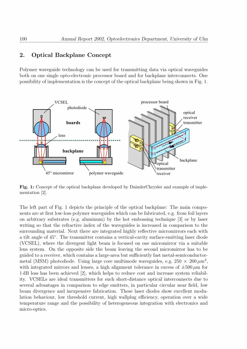
100 Annual Report 2002, Optoelectronics Department, University of Ulm
2. Optical Backplane Concept
Polymer waveguide technology can be used for transmitting data via optical waveguidesboth on one single opto-electronic processor board and for backplane interconnects. Onepossibility of implementation is the concept of the optical backplane being shown in Fig. 1.
Fig. 1: Concept of the optical backplane developed by DaimlerChrysler and example of imple-mentation [2].
The left part of Fig. 1 depicts the principle of the optical backplane: The main compo-nents are at first low-loss polymer waveguides which can be fabricated, e.g. from foil layerson arbitrary substrates (e.g. aluminum) by the hot embossing technique [3] or by laserwriting so that the refractive index of the waveguides is increased in comparison to thesurrounding material. Next there are integrated highly reflective micromirrors each witha tilt angle of 45. The transmitter contains a vertical-cavity surface-emitting laser diode(VCSEL), where the divergent light beam is focused on one micromirror via a suitablelens system. On the opposite side the beam leaving the second micromirror has to beguided to a receiver, which contains a large-area but sufficiently fast metal-semiconductor-metal (MSM) photodiode. Using large core multimode waveguides, e.g. 250 × 200µm2,with integrated mirrors and lenses, a high alignment tolerance in excess of ±500µm for1 dB loss has been achieved [2], which helps to reduce cost and increase system reliabil-ity. VCSELs are ideal transmitters for such short-distance optical interconnects due toseveral advantages in comparison to edge emitters, in particular circular near field, lowbeam divergence and inexpensive fabrication. These laser diodes show excellent modu-lation behaviour, low threshold current, high wallplug efficiency, operation over a widetemperature range and the possibility of heterogeneous integration with electronics andmicro-optics.
10 Gbit/s Data Transmission Experiments over Optical Backplane Waveguides 101
3. Parameters of the Laser Diode Transmitter
Top-emitting GaAs based 852 nm emission wavelength transverse multimode VCSELsfabricated by solid source molecular beam epitaxy are used for the transmission experi-ments. An AlAs layer included in the top mirror is selectively oxidized to define a currentaperture of 12µm. As seen in Fig. 2, threshold current and threshold voltage are 1.8 mAand 1.7 V, respectively. The differential resistance at 10 mA current amounts to 60 Ω andthe maximum output power at a bias current of 18.3 mA is 7.1 mW. The output spectrafor a CW driving current of 9 mA and under modulation with a 10 Gbit/s 27 − 1 pseudorandom bit sequence (PRBS) signal are highly multimode and centered around 852 nm.In both cases the root mean square spectral width is less than 0.4 nm. The measured3 dB bandwidth is 8.6 GHz at 9 mA which makes the device capable for 10 Gbit/s datatransmission.
Fig. 2: Operation characteristics of a 850 nm wavelength multimode VCSEL (left) and spectraat CW operation with different bias currents (right).
4. Dimensions of the Optical Backplanes
Three optical backplanes provided by the DaimlerChrysler Research Center have beeninvestigated. The backplane sample A has a total width of 12.5 cm and a length of35.8 cm. The cross-sectional area of the waveguide core is 250 × 200µm2. There are fourdifferent waveguide types, all with a numerical aperture (NA) of 0.35. Backplane sampleB has a total length of 191.5 cm and a width of 15.0 cm. As on sample A, some of thewaveguides are intersecting, and cross-section and NA of all waveguides are as mentionedbefore. On the backplane itself one can find five different waveguide types. Finally anoptical backplane sample C with a spiral waveguide was investigated. The core area ofthis 1 m-long waveguide is only 100 × 100µm2, NA is 0.3 and the minimum radius ofcurvature is about 4 cm.

102 Annual Report 2002, Optoelectronics Department, University of Ulm
5. Measurement Results
5.1 Waveguide attenuation
Since the waveguides are optimised for wavelengths around 850 nm, a VCSEL as describedin Sect. 3 was used for attenuation measurements. The attenuation is determined withoptimum coupling of the VCSEL light via two lenses and with a large-area photodetectorplaced directly above the output port. Figure 3 shows the attenuation values of thewaveguides on backplane samples A and B.
Fig. 3: Attenuation values of waveguides of backplane sample A (left) and sample B (right) at850 nm wavelength.
The observations can be summarised as follows:
Sample A: The longest waveguides (type 4) incorporate no bends and microlenses andthus show the lowest attenuation (< 2.25 dB). Assuming an insertion loss of 0.5 dB permirror [2], the measured minimum attenuation coefficient is as low as 2.2 dB/m.Sample B: Except for waveguide #7, the attenuation is higher or lower if the light iscoupled into the left or right waveguide end, respectively, which can be explained fromthe mirror fabrication process. The straight waveguide #6 of 50 cm length shows theminimum attenuation of 2.8 dB, which results in an attenuation coefficient of 3.6 dB/m ifthe insertion loss of two times 0.5 dB is taken into account.Sample C (spiral waveguide): The attenuation coefficient is the lowest one being measuredhere because of an improved fabrication process. The attenuation of 3 dB results in anattenuation coefficient of only 2 dB/m. This value is even smaller than the total loss of5 dB of a comparable 1 m-long spiral with 250 × 200µm2 core size [4].
5.2 Digital data transmission
For data transmission the VCSEL was driven at 9 mA bias. Transmission experimentshave been carried out with a PRBS non-return-to-zero signal of 27−1 word length (peak-to-peak voltage: 0.8 V; Bessel lowpass filter: fc = 7 GHz) at a data rate of 10 Gbit/s.

10 Gbit/s Data Transmission Experiments over Optical Backplane Waveguides 103
An InGaAs (p-i-n)-photoreceiver with either 50.0µm or 62.5µm multimode fiber (MMF)input was employed, where the larger fiber provides a higher coupling efficiency. Theinfluence of backreflection is negligible with measured average backreflection levels onsample A of −15.1 dB and −14.7 dB with and without microlenses, respectively. The meanbackreflection levels on backplane sample B and on the backplane spiral are −15.7 dB. Theeye diagrams are very similar for all experiments, so that the diagram corresponding tothe transmission over the backplane spiral is quite representative (Fig. 4). The eye is wideopen and essentially does not differ from the recorded eye diagram of the back-to-back(BTB) measurement. In both cases the received optical power is −13.7 dBm entailing abit error rate of BER < 10−12.
Fig. 4: Eye diagrams recorded for a BER < 10−12 at 10 Gbit/s data rate for BTB transmission(left) and over the backplane spiral (right).
In Fig. 5 BER curves are depicted for several different waveguides.
Sample A (250 × 200µm2): The lowest observed power penalty compared to the BTBmeasurement is 0.3 dB for waveguide #7 (23.5 cm) and for one of the waveguides #9(28 cm). The required optical power is −14.9 dBm and −15.7 dBm for waveguide #7 andfor the straight waveguide #9, respectively.Sample B (250 × 200µm2): The power penalty is 0.9 dB both for the straight waveguide#6 and for waveguide #7.Sample C (spiral waveguide, 100 × 100µm2): 10 Gbit/s transmission was possible overeven 1 m length which is consistent with a bit rate-length-product of more than 10 Gbit/s·mas extracted from small-signal measurements. The power penalty of 1.5 dB is relativelyhigh compared to only 0.5 dB for the 250 × 200µm2 spiral in [4].
6. Conclusion
The attenuation and data transmission characteristics of polymer waveguides for opti-cal backplane applications have been investigated. Quasi error-free transmission of a10 Gbit/s PRBS over 50 cm and 1 m-long waveguides has been demonstrated. The powerpenalty at a BER of 10−12 compared to BTB transmission was 0.9 dB for the larger

104 Annual Report 2002, Optoelectronics Department, University of Ulm
Fig. 5: BER characteristics for 27 − 1 word length PRBS transmission at 10 Gbit/s data rateover several waveguides (WGs), employing two different photoreceivers.
core waveguide and 1.5 dB for the smaller core waveguide. The attenuation of the spiralwaveguide has been the lowest one of all measured waveguides and is only about 2 dB/mat 850 nm wavelength. With regard to regular backreflection, no impact on the datatransmission characteristics has been observed at measured backreflection levels below−14.7 dB.
References
[1] R. Michalzik, “Optical backplanes, board and chip interconnects,” ch. 6 in Fiber OpticData Communication: Technological Trends and Advances, C. DeCusatis (Ed.), SanDiego: Academic Press, pp. 216–269, 2002.
[2] J. Moisel, J. Guttmann, H.-P. Huber, O. Krumpholz, and M. Rode, “Optical back-planes with integrated polymer waveguides,” Opt. Eng., vol. 39, no. 3, pp. 673–679,2000.
[3] S. Lehmacher and A. Neyer, “Integration of polymer optical waveguides into printedcircuit boards (PCB),” Electron. Lett., vol. 36, no. 12, pp. 1052–1053, 2000.
[4] F. Mederer, R. Michalzik, J. Guttmann, H.-P. Huber, B. Lunitz, J. Moisel, andD. Wiedenmann, “10 Gbit/s data transmission with TO-packaged multimode GaAsVCSELs over 1 m long polymer waveguides for optical backplane applications,” Opt.Comm., vol. 206, pp. 309–312, 2002.

1.55µm Wavelength VCSELs 105
Data Transmission with 1.55 µm Wavelength
InGaAlAs VCSELs
Felix Mederer, Robert Shau and Markus Ortsiefer ∗
We investigate high bit rate data transmission behavior of buried tunnel junction single-mode, linearly-polarized InGaAlAs VCSELs for 1.55µm wavelength. The devices showoutput powers of 0.73mW and maximum modulation bandwidths of 5.9GHz. We demon-strate 5Gbit/s data rate over 20.5 km standard single-mode fiber as well as 10Gbit/s forback-to-back transmission.
1. Introduction
Vertical-cavity surface-emitting lasers emitting at 850 nm wavelength are currently usedas transmitters for serial and parallel optical links over multimode fibers [1]. The ad-vantages of VCSELs are their high beam quality, longitudinal and transverse single-modeoperation, low power consumption and the possibility of array arrangements. Additionallyeasy on-wafer testing leads to low production and packaging costs. At 1.55µm wavelengthstandard single-mode fibers (SSMF) with high bandwidth length products and low opticaldispersion and attenuation can be used. Taking into account that the eye safety restric-tions at an emission wavelength of 1.55µm are relaxed by a factor of about 100 comparedto 850 nm wavelength [2], the maximum interconnect length can be up 80 km of SSMF[3, 4]. The technological challenges of monolithically grown 1.55µm wavelength VCSELsare the poor thermal conductivity and low reflectivities of InP-based Bragg mirrors. Ad-ditionally a natural oxidation process for current confinement is not yet known. As analternative to Bragg mirrors active regions on GaAs, metamorphic growth or wafer bond-ing techniques are conceivable. Using a substrate removal technique and bottom dielectricmirrors in combination with a buried tunnel junction (BTJ) for current confinement, asignificant improvement with respect to single-mode power and operation temperature hasbeen demonstrated [5]. In this paper we present the static and significantly improved dy-namic characteristics of InGaAlAs-based BTJ-VCSELs emitting at 1.55µm wavelength.For the first time we demonstrate 5 Gbit/s data transmission over 20.5 km SSMF as wellas 10 Gbit/s for back-to-back (BTB) operation. This shows the excellent performance of1.55µm VCSELs for Metropolitan Area Network applications.
∗The devices have been fabricated at the Walter Schottky Institut, Munich. M. Ortsiefer and R. Shauare now with VertiLas GmbH,Munich.

106 Annual Report 2002, Optoelectronics Department, University of Ulm
2. 1.55 µm Wavelength InGaAlAs VCSEL Layout
Figure 1 shows a schematic cross-sectional view of the BTJ-VCSEL.
n-contact
5 InGaAlAs QWs (8 nm)
SiO2
p-side contact +Au-coating
bottom Bragg mirror CaF / -Si2 a
top Bragg mirror InAlAs/InGaAlAs
Au-heatsink
n-InAlAs light
p-InAlAs
n-InP
n+-InGaAs
n+-InGaAs
p+-InGaAlAs
Fig. 1: Schematic layout of 1.55 µm InGaAlAs VCSELs.
The use of the BTJ leads to self-adjusted current confinement as well as optical confine-ment. Applying highly conductive n-doped spreading layers rather than highly resistivep-doped material, a low series resistances with associated small internal heating is ob-tained. The front and back mirrors consist of 34.5 pairs of epitaxial InGaAlAs and2.5 pairs of dielectric CaF2/a-Si stacks, respectively. The InP substrate on top of theupside-down mounted structure is completely removed. Despite of substrate removal, anelectroplated layer at the bottom ensures mechanical stability and additionally acts as anexcellent heatsink.
3. Static Characteristics
Figure 2 shows typical room temperature, continuous wave (CW) output characteristicsof 1.55 µm BTJ-VCSELs with an elliptic aperture of 3×4µm2.
0 1 2 3 4 5
Current (mA)
0.00
0.25
0.50
0.75
1.00
Ptot. P90°
P0°
Opti
cal
Pow
er (
mW
)
0.0
0.5
1.0
1.5
Volt
age
(V)
1535 1539
1 mA
0.5 mA
2 mA
3 mA 4 mA 5 mA
1543 1547
Wavelength (nm)
-90
-70
-50
-30
-10
Rel
. S
pec
tral
Pow
er (
dB
m)
Fig. 2: Operation characteristics of 1.55 µm InGaAlAs-VCSELs with an aperture size of3×4 µm2 (left) and spectra for different driving currents (right).
As shown on the left-hand side of Fig. 2, the maximum output power of this single-mode,single polarization device is 0.73 mW at 4.7 mA. The threshold voltage and threshold

1.55µm Wavelength VCSELs 107
current are as low as 0.91 V and 0.4 mA, respectively, while the differential series resis-tance is 78 Ω. The right-hand side of Fig. 2 shows the high resolution emission spectraof single-mode BTJ-VCSELs under CW operation. It is important to note that single-mode emission with at least 30 dB side-mode suppression-ratio (SMSR) can be observedover the entire current range. Due to internal heating, the peak wavelength shifts from1542.6 nm at 0.5 mA current to 1545.4 nm at 5 mA.
4. Dynamic Characteristics
The left-hand side of Fig. 3 shows the small-signal frequency responses of single-modeBTJ-VCSELs for various bias currents.
0
0.45 mA
0.6 mA0.7 mA
1.0 mA
1.5 mA
2 4 6 8 10
Frequency (GHz)
-30
-20
-10
0
10
Rel
. R
esp
on
se (
dB
)
0.5 mA
1510 1520 1530 1540 1550
Wavelength (nm)
-100
-60
-20
20
60
100
Rel
. S
pec
tral
Pow
er (
dB
m)
+60 dB
+0 dB
SMSR=37.5 dB
SMSR=37.8 dB
SMSR=37.9 dB
+120 dB
10 Gbit/s,V =0.16 VPP
10 Gbit/s,V =0.12 VPP
I =3 mACW
Fig. 3: Modulation response (left) and spectra for CW operation and with 10 Gbit/s modulation(right) of 1.55 µm InGaAlAs VCSELs with an aperture size of 3×4 µm2.
The maximum measured 3 dB modulation frequency of 5.9 GHz at 1.5 mA is limited byexternal parasitics, indicating necessary optimizations toward a high-frequency capableelectrical VCSEL layout. The right-hand side of Fig. 3 shows the emission spectra for CWoperation as well as for 10 Gbit/s modulation with Vpp = 0.12 V and Vpp = 0.16 V. Thepeak wavelengths for all cases are around 1543.1 nm, and SMSRs of more than 37 dB areobserved. The spectral width increases from δλRMS,CW = 0.0167 nm for CW operation toδλRMS,Vpp=0.16 V = 0.0567 nm.
5. Data Transmission over Standard Single-Mode Fibers
The 10 Gbit/s eye diagram on the left-hand side of Fig. 4 was recorded for BTB trans-mission with 3 mA bias current and a modulation with Vpp = 0.15 V. Even for very highbit rates of 10 Gbit/s, wide openings can be observed. As shown on the right-hand sideof Fig. 4, error-free data transmission with bit error rates (BER) of better than 10−12 isobtained up to data rates of 10 Gbit/s. For BTB operation at 5, 8 and 10 Gbit/s theminimum received optical power is −18.6 dBm, −15.4 dBm and −11.4 dBm, respectively.The measured power penalty for 5 Gbit/s data transmission over 20.5 km SSMF is about1 dB, while for 8 Gbit/s over 10.5 km SSMF the power penalty is only 0.4 dB.

108 Annual Report 2002, Optoelectronics Department, University of Ulm
20 ps/div
10
0 m
V/d
iv
10-12
10-10
10-8
10-6
10-4
10-2
-30 -25 -15 -5 +50
Bit
Err
or
Rate
-20 -10
5 Gbit/s, BTB
8 Gbit/s, BTB
10 Gbit/s, BTB
5 Gbit/s,
20.5 km SSMF
8 Gbit/s,
10.5 km SSMF
Fig. 4: 10 Gbit/s eye diagram after BTB transmission with 3 mA bias current and a modulationwith Vpp = 0.15 V (left) and bit error rates for 5, 8 and 10 Gbit/s data rates with 3 mA biascurrent and a modulation voltage of Vpp = 0.15 V (right).
6. Conclusion
We have demonstrated excellent output performance of single-mode, single polarizationBTJ InGaAlAs VCSELs emitting at 1.55µm wavelength for MAN applications. Measuredoutput power of 0.73 mW as well as a maximum modulation bandwidth of 5.9 GHz makesthese VCSELs capable to transmit 5 Gbit/s over 20.5 km SSMF and 8 Gbit/s over 10.5 kmSSMF with power penalties of only 1 dB and 0.4 dB, respectively. BTB transmission of10 Gbit/s was demonstrated for the first time with 1.55µm VCSELs.
References
[1] Infineon Technologies AG, “Parallel Optical Links (PAROLI),” Jan. 2003. Online:http://www.infineon.com/cgi/ecrm.dll/ecrm/scripts/prod cat.jsp?oid=-8222.
[2] Berufsgenossenschaft der Feinmechanik und Elektrotechnik, “BG-Vorschriften / Un-fallverhutungsvorschriften, B 2, Laserstrahlung,” Berufsgenossenschaft der Fein-mechanik und Elektrotechnik, Referat Strahlenschutz, Januar 1993.
[3] 10GE Alliance, “10 Gigabit Ethernet Technology Overview White Paper, Re-vision 2, Draft A.” 10gea white paper 0502.pdf, 10 April 2002. Online:http://www.10gea.org/.
[4] American National Standards Institute, Committee T1, “Synchronous OpticalNetwork (SONET) – Physical Layer Specification (Revision of ANSI 1.106-1988):T1.105.06-1996,” American National Standards Institute, Committee T1X1,Mar. 1996.
[5] R. Shau, M. Ortsiefer, J. Rosskopf, G. Bohm, F. Kohler, and M.-C Amann, “Vertical-Cavity Surface-Emitting Laser Diodes at 1.55 µm with Large Output Power and HighOperation Temperature,” Electron. Lett., vol. 37, pp. 1295–1296, Oct. 2001.

Ph.D. Theses 109
Ph.D. Theses
1. Stefan Bader,Entwicklung und Charakterisierung einer GaN-basierenden LaserdiodeWork performed at OSRAM Opto Semiconductors, Regensburg, Germany04.03.2002
2. Safwat W.Z. Mahmoud,Static and dynamic transverse mode characteristics of vertical-cavity surface-emittingsemiconductor lasers10.06.2002
3. Michael Miller,Aufbautechnik, Leistungsskalierung und Strahlformung oberflachenemittierender Halb-leiterlaserMounting technique, scaling of optical output power, and beam shaping of surface-emitting semiconductor laser diodes29.06.2002
4. Gunther Steinle,Neuartige monolithische InAlGaAsN VertikallaserdiodenWork performed at Infineon Technologies AG, Munchen, Germany01.07.2002
5. Roland Jager,Molekularstrahleptiaxie hocheffizienter Leucht- und Laserdioden29.07.2002
6. Ulrich Martin,Emissions- und Alterungsverhalten von transversal einmodigen, kantenemittieren-den Halbleiter-Laserdioden15.11.2002

110 Annual Report 2002, Optoelectronics Department, University of Ulm
Diploma and Master Theses
1. Barbara Neubert,Optimierung der Prozesstechnologie zur Herstellung von getaperten InAlGaP Leucht-diodenDiploma thesis, Optoelectronics Department, January 2002
2. Hendrik Roscher,Prozessentwicklung fur die Flip-Chip Montage von Vertikallaserdiodenmatrizen mitEmissionswellenlangen von 850 nmDiploma thesis, Optoelectronics Department, March 2002
3. Martin Stach,Charakterisierung von optischen Datenubertragungsstrecken mit sichtbaren und infra-roten VertikallaserdiodenDiploma thesis, Optoelectronics Department, April 2002
4. Eduardo Gomez-Henning,Fabrication and characterization of single-mode ridge-waveguide semiconductor lasersMaster thesis in Communications Technology, Optoelectronics Department, April2002
5. Michael Furitsch,Charakterisierung auf InAlGaP basierender Hochleistungs-KantenemitterDiploma thesis, Osram Opto Semiconductors, July 2002
6. Ferdous Karim Khan,Design, fabrication, and characterization of surface-etched polarization-stable single-mode VCSELsDiploma thesis, Optoelectronics Department, September 2002
7. Karl Felix Antritter,Charakterisierung von optisch gepumpten Halbleiter-ScheibenlasersystemenDiploma thesis, Optoelectronics Department, October 2002

Semester Projects 111
Semester Projects
1. Philipp Gerlach,Aufbau eines nach der Feedforward-Methode linearisierten LasersystemsFebruary 2002
2. Stefan Buntz,Aufbau und Inbetriebnahme eines Messplatzes zur Analyse der spektralen Eigen-schaften von Vertikallaserdioden unter GroßsignalmodulationMay 2002
3. Martin Fuchs,Aufbau eines 10BaseT-kompatiblen Freistrahl-Datenubertragungssystems mit Ver-tikallaserdiodenMay 2002
4. Peter Bruckner,Herstellung und Untersuchung von InGaAlP Leuchtdioden mit variierenden Taper-winkelnJuly 2002
5. Lothar Schlafer,Berechnung von Eigenwellen in Multi-Mode-Glasfasern mit GradientenindexprofilAugust 2002
6. Christoph Schleifer,Aufbau einer modularen Messeinheit zur Charakterisierung von VertikallaserdiodenSeptember 2002
7. Markus Thal,Entwicklung und Aufbau eines temperaturgeregelten Heiztisches fur die On-WaferCharakterisierung von optoelektronischen HalbleiterbauelementenNovember 2002
8. Michael Schumann,Messungen zur Modenausbreitung in mehrmodigen Glasfasern mit dem Differential-Mode-Delay VerfahrenDecember 2002
112 Annual Report 2002, Optoelectronics Department, University of Ulm
Talks
[1] F.S. Habel and M. Seyboth, “Defektanalyse von GaN-ELOG Strukturen mit Hilfevon HCl-Atzprozessen,” 17. Workshop Epitaxie von III/V-Halbleitern, DGKK 2002,Magdeburg, Germany, Dec. 2002.
[2] T. Knodl, M. Golling, A. Straub, R. Michalzik, and K.J. Ebeling, “Multi-stageVCSELs: theory and experiment,” Infineon Technologies, Munich, Germany, July2002.
[3] T. Knodl, M. Golling, A. Straub, R. Michalzik, and K.J. Ebeling, “Development andinvestigation of bipolar cascade VCSELs,” Institute of Quantum Electronics, ETHZurich, Zurich, Switzerland, Nov. 2002.
[4] R. Michalzik, I. Kardosh, M. Kicherer, F. Mederer, M. Riedl, H. Roscher, M. Stach,H.J. Unold, and K.J. Ebeling, “VCSEL arrays for high-speed interconnect and high-power applications,” Edith Cowan University, School of Engineering and Mathemat-ics, Joondalup, Western Australia, Nov. 2002.
[5] R. Michalzik, I. Kardosh, M. Kicherer, T. Knodl, F. Mederer, M. Riedl, H. Roscher,M. Stach, H.J. Unold, and K.J. Ebeling, “VCSEL-related research at the Universityof Ulm,” Sony Corporation, Atsugi Technology Center, Kanagawa, Japan, Oct. 2002.
[6] R. Michalzik, I. Kardosh, M. Kicherer, F. Mederer, M. Riedl, H. Roscher, M. Stach,H.J. Unold, and K.J. Ebeling, “Optical interconnect research activities at Ulm Uni-versity,” Nippon Telegraph and Telephone Corporation, NTT Microsystem IntegrationLaboratories, Kanagawa, Japan, Oct. 2002.
[7] R. Michalzik, I. Kardosh, M. Kicherer, T. Knodl, F. Mederer, M. Riedl, H. Roscher,M. Stach, H.J. Unold, and K.J. Ebeling, “Short-wavelength VCSEL applications:datacom and more,” Tokyo Institute of Technology, Precision & Intelligence Labora-tory, Yokohama, Japan, Oct. 2002.
[8] P. Unger, “Halbleiterlaser und optoelektronische Systeme,” Halbleiterkolloquium derTechnischen Universitat Braunschweig, Braunschweig, Germany, Jan. 2002.
[9] P. Unger, “Halbleiterlaser und optoelektronische Systeme,” Kolloquium “Optoelek-tronische Bauelemente” der Technischen Universitat Dresden, Dresden, Germany,Feb. 2002.
[10] P. Unger, “Halbleiterlaser fur hohe optische Ausgangsleistung,” Kolloquium “Strahl-werkzeuge” der Universitat Stuttgart, Stuttgart, Germany, Apr. 2002.
[11] P. Unger, “Optisch gepumpte Halbleiter-Scheibenlaser,” Oberseminar des Physikalis-chen Institutes der Universitat Stuttgart, Stuttgart, Germany, June 2002.
Publications and Conference Contributions 113
Publications and Conference Contributions
[1] E. Deichsel, R. Jager, and P. Unger, “High-brightness unstable-resonator lasers fab-ricated with improved dry-etching technology for ultra-smooth laser facets,” Jpn. J.Appl. Phys., vol. 41, pp. 4279–4282, 2002.
[2] E. Deichsel, R. Jager, and P. Unger, “5 W in a multi-mode fiber from a single 980-nm-emitting laser diode,” in Proc. European Conference on Optical Communication,ECOC 2002, vol. 3, Copenhagen, Denmark, poster P2.22, Sep. 2002.
[3] E. Deichsel and P. Unger, “Semiconductor unstable-resonator laser diodes for high-power and high-brightness applications,” in Semiconductor Lasers and Applications,Y. Luo and Y. Nakano (Eds.), Proc. SPIE, vol. 4913, pp. 90–97, 2002.
[4] E. Deichsel and P. Unger, “Dry-etching in optoelectronic device fabrication usingchemically-assisted ion-beam etching,” in Tech. Digest Compound SemiconductorManufacturing Expo, CS-MAX 2002, San Jose, CA, USA, pp. 29–31, Nov. 2002.
[5] I. Ecker, S. Menzel, J. Joos, I. Kardosh, R. Michalzik, and K.J. Ebeling, “Growthof GaAsSb/GaAs double quantum well lasers emitting near 1.3µm,” in Proc. 44thElectronic Materials Conf., EMC 2002, Santa Barbara, CA, USA, p. 6, June 2002.
[6] P.S. Ivanov, H.J. Unold, R. Michalzik, F. Mederer, J. Maehnss, K.J. Ebeling, andI. Sukhoivanov, “Theoretical investigation of transverse modes in photonic crystalsurface-emitting lasers,” in Proc. 4th Int.’l Conf. on Transparent Optical Networks,ICTON 2002, vol. 2, Warsaw, Poland, pp. 136–139, April 2002.
[7] P.S. Ivanov, H.J. Unold, R. Michalzik, J. Maehnss, K.J. Ebeling, and I. Sukhoivanov,“Application of photonic crystal effective index model for defining single-modeconditions in PCSELs,” in Proc. IEEE Lasers and Electro-Opt. Soc. Ann. Meet.,LEOS 2002, vol. 1, Glasgow, Scotland, pp. 221–222, Nov. 2002.
[8] P.S. Ivanov, H.J. Unold, R. Michalzik, J. Maehnss, K.J. Ebeling, and I. Sukhoivanov,“Single-mode conditions in photonic crystal vertical-cavity surface-emitting lasers,”in Proc. Workshop on Laser and Fiber-Optical Networks Modelling, LFNM 2001,Kharkov, Ukraine, pp. 141–144, June 2002.
[9] P.S. Ivanov, H. Unold, A.V. Shulika, A.V. Kublik, and I.A. Sukhoivanov, “Lightlocalization in a defect of the photonic crystal,” Radioelektronika i informatika (inRussian), pp. 42–45, 2002.
[10] P.S. Ivanov, H. Unold, V.V. Lysak, and I.A. Sukhoivanov, “Using photonic crystals inoptical communication systems,” Radioelektronika i informatika (in Russian), pp. 34–37, 2002.

114 Annual Report 2002, Optoelectronics Department, University of Ulm
[11] M. Kicherer, A. Fiore, U. Oesterle, R.P. Stanley, M. Ilegems, and R. Michalzik, “Datatransmission using GaAs-based InAs-InGaAs quantum dot LEDs emitting at 1.3µmwavelength,” Electron. Lett., vol. 38, pp. 906–907, 2002.
[12] T. Knodl, M. Golling, M. Kicherer, R. Michalzik, and K.J. Ebeling, “Three-terminaldual-stage vertical-cavity surface-emitting laser,” Electron. Lett., vol. 38, pp. 278–280, 2002.
[13] T. Knodl, M. Golling, R. Michalzik, and K.J. Ebeling, “Bistability in bipolar cascadeVCSELs,” Electron. Lett., vol. 38, pp. 370–371, 2002.
[14] T. Knodl, R. Michalzik, M. Golling, and K.J. Ebeling, “Current-spreading-inducedbistability in bipolar cascade vertical-cavity surface-emitting lasers,” Appl. Phys.Lett., vol. 81, pp. 583–585, 2002.
[15] F. Mederer, I. Ecker, R. Michalzik, G. Steinle, H. Riechert, K.J. Ebeling, B. Lu-nitz, J. Moisel, and D. Wiedenmann, “VCSEL transmitters for 10-Gigabit Ether-net: 1.3µm wavelength VCSELs for metropolitan-area-networks and TO-packaged850 nm wavelength VCSELs for data transmission over multimode fibers and opticalbackplane-waveguides,” in Proc. 52nd Electronic Components & Technology Con-ference, ECTC 2002, San Diego, CA, USA, pp. 5–11, May 2002.
[16] F. Mederer, R. Michalzik, J. Guttmann, H.P. Huber, B. Lunitz, J. Moisel, andD. Wiedenmann, “10 Gb/s data transmission with TO-packaged multimode GaAsVCSELs over 1 m long polymer waveguides for optical backplane applications,” Op-tics Communications, vol. 206, pp. 309–312, 2002.
[17] R. Michalzik, “Optical backplanes, board and chip interconnects,” Chap. 6 in FiberOptic Data Communication: Technological Trends and Advances, C. DeCusatis(Ed.), pp. 216–269, San Diego: Academic Press, 2002.
[18] R. Michalzik, K.J. Ebeling, M. Kicherer, T. Knodl, S.W.Z. Mahmoud, F. Mederer,M. Riedl, H. Roscher, M. Stach, and H.J. Unold, “VCSEL technologies for datacom,”in Proc. 3rd Int.’l Conf. on Optics-Photonics Design & Fabrication, ODF 2002, (in-vited), Tokyo, Japan, pp. 33–34, Oct. 2002.
[19] R. Michalzik, F. Mederer, H. Roscher, M. Stach, H. Unold, D. Wiedenmann, R. King,M. Grabherr, and E. Kube, “Design and communication applications of short-wavelength VCSELs ,” in Materials and Devices for Optical and Wireless Commu-nications, C.J. Chang-Hasnain, Y. Xia, and K. Iga (Eds.), (invited), Proc. SPIE,vol. 4905, pp. 310–321, 2002.
[20] D. Mistele, T. Rotter, K.S. Rover, S. Paprotta, M. Seyboth, V. Schwegler, F. Fedler,H. Klausing, O.K. Semchinova, J. Stemmer, J. Aderhold, and J. Graul, “First Al-GaN/GaN MOSFET with photoanodic gate dielectric,” Mat. Sci. Eng., vol. B93,pp. 107–111, 2002.

Publications and Conference Contributions 115
[21] D. Mistele, T. Rotter, Z. Bougrioua, I. Moermann, K.S. Rover, M. Seyboth,V. Schwegler, J. Stemmer, F. Fedler, H. Klausing, O.K. Semchinova, J. Aderhold,and J. Graul, “AlGaN/GaN based MOSHFETs with different gate dielectrics andtreatments,” in Proc. Mat. Res. Soc. Symp., vol. 693, Boston, MA, USA, pp. I6.51.1–I6.51.6, Nov. 2002.
[22] P. Unger, “High-power laser diodes and laser diode arrays,” Chap. 2.4 in Handbookof Lasers, Part B, 2003, to be published by IOP Publishing.
[23] M. Scherer, B. Neubert, S.S. Schad, W. Schmid, C. Karnutsch, W. Wegleiter,A. Plossl, and K.P. Streubel, “Efficient InAlGaP light-emitting diodes using radialoutcoupling taper,” in Light-Emitting Diodes: Research, Manufacturing and Appli-cations VI, E.F. Schubert and H.W. Yao (Eds.), Proc. SPIE, vol. 4641, pp. 31–41,2002.
[24] E. Schiehlen, M. Golling, and P. Unger, “Diode-pumped semiconductor disk laserwith intracavity frequency doubling using Lithium Triborate (LBO),” IEEE Photon.Technol. Lett., vol. 14, pp. 777–779, 2002.
[25] E. Schiehlen and P. Unger, “Diode-pumped vertical external cavity surface emittinglaser,” in Proc. Second Joint Symposium on Opto- & Microelectronic Devices andCircuits, SODC 2002, Stuttgart, Germany, pp. 104–109, Mar. 2002.
[26] M. Seyboth, S.S. Schad, M. Scherer, F. Habel, C. Eichler, M. Kamp, and V. Schweg-ler, “Substrates for wide bandgap nitrides,” J. Mat. Sci.: Materials in Electronics,vol. 13, pp. 659–664, 2002.
[27] M. Stach, F. Mederer, R. Michalzik, B. Lunitz, J. Moisel, and D. Wiedenmann,“10 Gbit/s data transmission experiments over optical backplane waveguides with850 nm wavelength multimode VCSELs,” in Proc. 7th Workshop of Optics in Com-puting Technology, ORT 2002, Mannheim, Germany, pp. 47–54, Sep. 2002.
[28] H.J. Unold, S.W.Z. Mahmoud, R. Jager, M. Golling, M. Kicherer, F. Mederer, M.C.Riedl, T. Knodl, M. Miller, R. Michalzik, and K.J. Ebeling, “Single-mode VCSELs,”in Vertical-Cavity Surface-Emitting Lasers VI, C. Lei and S.P. Kilcoyne (Eds.), Proc.SPIE, vol. 4649, pp. 218–229, 2002.
[29] H.J. Unold, M.C. Riedl, R. Michalzik, and K.J. Ebeling, “Polarization control inVCSELs by elliptic surface etching,” Electron. Lett., vol. 38, pp. 77–78, 2002.
[30] H.J. Unold, P. Debernardi, R. Michalzik, F.K. Khan, and K.J. Ebeling, “Design andmodeling of polarization-stable surface-etched VCSELs,” in Proc. 18th IEEE Int.’lSemiconductor Laser Conference, ISLC 2002, Garmisch-Partenkirchen, Germany,pp. 15–16, Sep./Oct. 2002.

116 Annual Report 2002, Optoelectronics Department, University of Ulm
[31] S. Barland, J.R. Tredicce, M. Brambilla, L.A. Lugiato, S. Balle, M. Giudici, T. Mag-gipinto, L. Spinelli, G. Tissoni, T. Knodl, M. Miller, and R. Jager, “Cavity solitonsas pixels in semiconductor microcavities,” Nature, vol. 419, pp. 699–702, 2002.
[32] B. Corbett, P. Lambkin, J. Justice, E. Deichsel, and P. Unger, “Internal focus 980 nmunstable resonator laser diodes,” in Proc. IEEE Lasers and Electro-Opt. Soc. Ann.Meet., LEOS 2002, vol. 2, Glasgow, Scotland, pp. 649–650, Nov. 2002.
[33] A. Knigge, M. Zorn, H.J. Unold, F. Mederer, M. Weyers, and G. Trankle, “High-performance vertical-cavity surface-emitting lasers with emission wavelengths from650 nm to 670 nm,” in Proc. 18th IEEE Int’l Semiconductor Laser Conference, ISLC2002, Garmisch-Partenkirchen, Germany, pp. 7–8, Sep./Oct. 2002.
[34] M. Ortsiefer, R. Shau, F. Mederer, R. Michalzik, J. Roßkopf, G. Bohm, F. Kohler,C. Lauer, M. Maute, and M.C. Amann, “High-speed data transmission with 1.55µmvertical-cavity surface-emitting lasers,” in Proc. 28th European Conference on OpticalCommunication, ECOC 2002, post-deadline paper PD4.9, Copenhagen, Denmark,Sep. 2002.
[35] M. Ortsiefer, R. Shau, F. Mederer, R. Michalzik, J. Rosskopf, G. Bohm, F. Kohler,C. Lauer, M. Maute, and M.C. Amann, “High-speed modulation up to 10 Gbit/swith 1.55µm wavelength InGaAlAs VCSELs,” Electron. Lett., vol. 38, pp. 1180–1181, 2002.
[36] S. Riyopoulos and H. Unold, “Theoretical interpretation of the enhanced single-mode stability in extended cavity VCSELs,” IEEE J. Lightwave Technol., vol. 20,pp. 1173–1181, 2002.
[37] W. Schmid, M. Scherer, C. Karnutsch, A. Ploßl, W. Wegleiter, S.S. Schad, B. Neu-bert, and K. Streubel, “High efficiency, red and infrared light-emitting diodes usingradial outcoupling taper,” IEEE J. Select. Top. Quantum Electron., vol. 8, pp. 256–263, 2002.
[38] B. Stegmuller, E. Baur, and M. Kicherer, “1.55µm and 1.3µm DFB lasers inte-grated with electro absorption modulators for high-speed transmission systems,” inProc. Second Joint Symposium on Opto- & Microelectronic Devices and Circuits,SODC 2002, Stuttgart, Germany, pp. 95–99, Mar. 2002.
[39] B. Stegmuller, E. Baur, and M. Kicherer, “15-GHz modulation performance of inte-grated DFB laser diode EA modulator with identical multiple-quantum-well double-stack active layer,” Photon. Technol. Lett., vol. 14, pp. 1647–1649, 2002.